JP4457694B2 - Heat dissipation structure for electronic components - Google Patents
Heat dissipation structure for electronic componentsDownload PDFInfo
- Publication number
- JP4457694B2 JP4457694B2JP2004046826AJP2004046826AJP4457694B2JP 4457694 B2JP4457694 B2JP 4457694B2JP 2004046826 AJP2004046826 AJP 2004046826AJP 2004046826 AJP2004046826 AJP 2004046826AJP 4457694 B2JP4457694 B2JP 4457694B2
- Authority
- JP
- Japan
- Prior art keywords
- grease
- case
- circuit board
- electronic component
- heat dissipation
- Prior art date
- Legal status (The legal status is an assumption and is not a legal conclusion. Google has not performed a legal analysis and makes no representation as to the accuracy of the status listed.)
- Expired - Fee Related
Links
Images


Classifications
- H—ELECTRICITY
- H05—ELECTRIC TECHNIQUES NOT OTHERWISE PROVIDED FOR
- H05K—PRINTED CIRCUITS; CASINGS OR CONSTRUCTIONAL DETAILS OF ELECTRIC APPARATUS; MANUFACTURE OF ASSEMBLAGES OF ELECTRICAL COMPONENTS
- H05K1/00—Printed circuits
- H05K1/02—Details
- H05K1/0201—Thermal arrangements, e.g. for cooling, heating or preventing overheating
- H05K1/0203—Cooling of mounted components
- H05K1/0204—Cooling of mounted components using means for thermal conduction connection in the thickness direction of the substrate
- H05K1/0206—Cooling of mounted components using means for thermal conduction connection in the thickness direction of the substrate by printed thermal vias
- H—ELECTRICITY
- H01—ELECTRIC ELEMENTS
- H01L—SEMICONDUCTOR DEVICES NOT COVERED BY CLASS H10
- H01L23/00—Details of semiconductor or other solid state devices
- H01L23/34—Arrangements for cooling, heating, ventilating or temperature compensation ; Temperature sensing arrangements
- H01L23/36—Selection of materials, or shaping, to facilitate cooling or heating, e.g. heatsinks
- H01L23/367—Cooling facilitated by shape of device
- H01L23/3677—Wire-like or pin-like cooling fins or heat sinks
- H—ELECTRICITY
- H01—ELECTRIC ELEMENTS
- H01L—SEMICONDUCTOR DEVICES NOT COVERED BY CLASS H10
- H01L23/00—Details of semiconductor or other solid state devices
- H01L23/34—Arrangements for cooling, heating, ventilating or temperature compensation ; Temperature sensing arrangements
- H01L23/42—Fillings or auxiliary members in containers or encapsulations selected or arranged to facilitate heating or cooling
- H—ELECTRICITY
- H01—ELECTRIC ELEMENTS
- H01L—SEMICONDUCTOR DEVICES NOT COVERED BY CLASS H10
- H01L2224/00—Indexing scheme for arrangements for connecting or disconnecting semiconductor or solid-state bodies and methods related thereto as covered by H01L24/00
- H01L2224/01—Means for bonding being attached to, or being formed on, the surface to be connected, e.g. chip-to-package, die-attach, "first-level" interconnects; Manufacturing methods related thereto
- H01L2224/02—Bonding areas; Manufacturing methods related thereto
- H01L2224/04—Structure, shape, material or disposition of the bonding areas prior to the connecting process
- H01L2224/05—Structure, shape, material or disposition of the bonding areas prior to the connecting process of an individual bonding area
- H01L2224/0554—External layer
- H01L2224/05599—Material
- H—ELECTRICITY
- H01—ELECTRIC ELEMENTS
- H01L—SEMICONDUCTOR DEVICES NOT COVERED BY CLASS H10
- H01L2224/00—Indexing scheme for arrangements for connecting or disconnecting semiconductor or solid-state bodies and methods related thereto as covered by H01L24/00
- H01L2224/01—Means for bonding being attached to, or being formed on, the surface to be connected, e.g. chip-to-package, die-attach, "first-level" interconnects; Manufacturing methods related thereto
- H01L2224/42—Wire connectors; Manufacturing methods related thereto
- H01L2224/44—Structure, shape, material or disposition of the wire connectors prior to the connecting process
- H01L2224/45—Structure, shape, material or disposition of the wire connectors prior to the connecting process of an individual wire connector
- H01L2224/45001—Core members of the connector
- H01L2224/45099—Material
- H—ELECTRICITY
- H01—ELECTRIC ELEMENTS
- H01L—SEMICONDUCTOR DEVICES NOT COVERED BY CLASS H10
- H01L2224/00—Indexing scheme for arrangements for connecting or disconnecting semiconductor or solid-state bodies and methods related thereto as covered by H01L24/00
- H01L2224/01—Means for bonding being attached to, or being formed on, the surface to be connected, e.g. chip-to-package, die-attach, "first-level" interconnects; Manufacturing methods related thereto
- H01L2224/42—Wire connectors; Manufacturing methods related thereto
- H01L2224/47—Structure, shape, material or disposition of the wire connectors after the connecting process
- H01L2224/48—Structure, shape, material or disposition of the wire connectors after the connecting process of an individual wire connector
- H01L2224/4805—Shape
- H01L2224/4809—Loop shape
- H01L2224/48091—Arched
- H—ELECTRICITY
- H01—ELECTRIC ELEMENTS
- H01L—SEMICONDUCTOR DEVICES NOT COVERED BY CLASS H10
- H01L2224/00—Indexing scheme for arrangements for connecting or disconnecting semiconductor or solid-state bodies and methods related thereto as covered by H01L24/00
- H01L2224/01—Means for bonding being attached to, or being formed on, the surface to be connected, e.g. chip-to-package, die-attach, "first-level" interconnects; Manufacturing methods related thereto
- H01L2224/42—Wire connectors; Manufacturing methods related thereto
- H01L2224/47—Structure, shape, material or disposition of the wire connectors after the connecting process
- H01L2224/48—Structure, shape, material or disposition of the wire connectors after the connecting process of an individual wire connector
- H01L2224/481—Disposition
- H01L2224/48151—Connecting between a semiconductor or solid-state body and an item not being a semiconductor or solid-state body, e.g. chip-to-substrate, chip-to-passive
- H01L2224/48221—Connecting between a semiconductor or solid-state body and an item not being a semiconductor or solid-state body, e.g. chip-to-substrate, chip-to-passive the body and the item being stacked
- H01L2224/48245—Connecting between a semiconductor or solid-state body and an item not being a semiconductor or solid-state body, e.g. chip-to-substrate, chip-to-passive the body and the item being stacked the item being metallic
- H01L2224/48247—Connecting between a semiconductor or solid-state body and an item not being a semiconductor or solid-state body, e.g. chip-to-substrate, chip-to-passive the body and the item being stacked the item being metallic connecting the wire to a bond pad of the item
- H—ELECTRICITY
- H01—ELECTRIC ELEMENTS
- H01L—SEMICONDUCTOR DEVICES NOT COVERED BY CLASS H10
- H01L2224/00—Indexing scheme for arrangements for connecting or disconnecting semiconductor or solid-state bodies and methods related thereto as covered by H01L24/00
- H01L2224/80—Methods for connecting semiconductor or other solid state bodies using means for bonding being attached to, or being formed on, the surface to be connected
- H01L2224/85—Methods for connecting semiconductor or other solid state bodies using means for bonding being attached to, or being formed on, the surface to be connected using a wire connector
- H01L2224/8538—Bonding interfaces outside the semiconductor or solid-state body
- H01L2224/85399—Material
- H—ELECTRICITY
- H01—ELECTRIC ELEMENTS
- H01L—SEMICONDUCTOR DEVICES NOT COVERED BY CLASS H10
- H01L24/00—Arrangements for connecting or disconnecting semiconductor or solid-state bodies; Methods or apparatus related thereto
- H01L24/01—Means for bonding being attached to, or being formed on, the surface to be connected, e.g. chip-to-package, die-attach, "first-level" interconnects; Manufacturing methods related thereto
- H01L24/42—Wire connectors; Manufacturing methods related thereto
- H01L24/47—Structure, shape, material or disposition of the wire connectors after the connecting process
- H01L24/48—Structure, shape, material or disposition of the wire connectors after the connecting process of an individual wire connector
- H—ELECTRICITY
- H01—ELECTRIC ELEMENTS
- H01L—SEMICONDUCTOR DEVICES NOT COVERED BY CLASS H10
- H01L2924/00—Indexing scheme for arrangements or methods for connecting or disconnecting semiconductor or solid-state bodies as covered by H01L24/00
- H01L2924/0001—Technical content checked by a classifier
- H01L2924/00014—Technical content checked by a classifier the subject-matter covered by the group, the symbol of which is combined with the symbol of this group, being disclosed without further technical details
- H—ELECTRICITY
- H01—ELECTRIC ELEMENTS
- H01L—SEMICONDUCTOR DEVICES NOT COVERED BY CLASS H10
- H01L2924/00—Indexing scheme for arrangements or methods for connecting or disconnecting semiconductor or solid-state bodies as covered by H01L24/00
- H01L2924/15—Details of package parts other than the semiconductor or other solid state devices to be connected
- H01L2924/181—Encapsulation
- H—ELECTRICITY
- H05—ELECTRIC TECHNIQUES NOT OTHERWISE PROVIDED FOR
- H05K—PRINTED CIRCUITS; CASINGS OR CONSTRUCTIONAL DETAILS OF ELECTRIC APPARATUS; MANUFACTURE OF ASSEMBLAGES OF ELECTRICAL COMPONENTS
- H05K2201/00—Indexing scheme relating to printed circuits covered by H05K1/00
- H05K2201/09—Shape and layout
- H05K2201/09009—Substrate related
- H05K2201/09054—Raised area or protrusion of metal substrate
- H—ELECTRICITY
- H05—ELECTRIC TECHNIQUES NOT OTHERWISE PROVIDED FOR
- H05K—PRINTED CIRCUITS; CASINGS OR CONSTRUCTIONAL DETAILS OF ELECTRIC APPARATUS; MANUFACTURE OF ASSEMBLAGES OF ELECTRICAL COMPONENTS
- H05K2201/00—Indexing scheme relating to printed circuits covered by H05K1/00
- H05K2201/09—Shape and layout
- H05K2201/09209—Shape and layout details of conductors
- H05K2201/095—Conductive through-holes or vias
- H05K2201/0959—Plated through-holes or plated blind vias filled with insulating material
- H—ELECTRICITY
- H05—ELECTRIC TECHNIQUES NOT OTHERWISE PROVIDED FOR
- H05K—PRINTED CIRCUITS; CASINGS OR CONSTRUCTIONAL DETAILS OF ELECTRIC APPARATUS; MANUFACTURE OF ASSEMBLAGES OF ELECTRICAL COMPONENTS
- H05K2201/00—Indexing scheme relating to printed circuits covered by H05K1/00
- H05K2201/10—Details of components or other objects attached to or integrated in a printed circuit board
- H05K2201/10007—Types of components
- H05K2201/10166—Transistor
- H—ELECTRICITY
- H05—ELECTRIC TECHNIQUES NOT OTHERWISE PROVIDED FOR
- H05K—PRINTED CIRCUITS; CASINGS OR CONSTRUCTIONAL DETAILS OF ELECTRIC APPARATUS; MANUFACTURE OF ASSEMBLAGES OF ELECTRICAL COMPONENTS
- H05K3/00—Apparatus or processes for manufacturing printed circuits
- H05K3/40—Forming printed elements for providing electric connections to or between printed circuits
- H05K3/42—Plated through-holes or plated via connections
- H05K3/429—Plated through-holes specially for multilayer circuits, e.g. having connections to inner circuit layers
- Y—GENERAL TAGGING OF NEW TECHNOLOGICAL DEVELOPMENTS; GENERAL TAGGING OF CROSS-SECTIONAL TECHNOLOGIES SPANNING OVER SEVERAL SECTIONS OF THE IPC; TECHNICAL SUBJECTS COVERED BY FORMER USPC CROSS-REFERENCE ART COLLECTIONS [XRACs] AND DIGESTS
- Y10—TECHNICAL SUBJECTS COVERED BY FORMER USPC
- Y10T—TECHNICAL SUBJECTS COVERED BY FORMER US CLASSIFICATION
- Y10T428/00—Stock material or miscellaneous articles
- Y10T428/31504—Composite [nonstructural laminate]
- Y10T428/31678—Of metal
- Y10T428/31681—Next to polyester, polyamide or polyimide [e.g., alkyd, glue, or nylon, etc.]
Landscapes
- Engineering & Computer Science (AREA)
- Microelectronics & Electronic Packaging (AREA)
- Physics & Mathematics (AREA)
- Condensed Matter Physics & Semiconductors (AREA)
- General Physics & Mathematics (AREA)
- Computer Hardware Design (AREA)
- Power Engineering (AREA)
- Chemical & Material Sciences (AREA)
- Materials Engineering (AREA)
- Cooling Or The Like Of Electrical Apparatus (AREA)
- Cooling Or The Like Of Semiconductors Or Solid State Devices (AREA)
Description
Translated fromJapanese本発明は、発熱を伴う電子部品と、電子部品を搭載する回路基板と、回路基板を収容するケースと、電子部品もしく回路基板とケースの間に介在するグリースとを有する電子部品の放熱構造に関する。 The present invention relates to an electronic component heat dissipation structure including an electronic component that generates heat, a circuit board on which the electronic component is mounted, a case that houses the circuit board, and an electronic component or grease that is interposed between the circuit board and the case. About.
回路基板に実装した発熱を伴う電子部品から放熱させるには、従来、発熱素子(パワートランジスタ等)に放熱板を取り付けて、放熱させていた。しかし、このような放熱構造は、放熱板の取り付けにコストがかかった。また、SMD(Surface Mount Device)タイプのパワー素子からは放熱できないといった問題がある。 In order to dissipate heat from an electronic component with heat generation mounted on a circuit board, a heat dissipating plate (power transistor or the like) is conventionally attached to the heat generating element to dissipate heat. However, such a heat dissipation structure is costly to attach the heat dissipation plate. Further, there is a problem that heat cannot be radiated from an SMD (Surface Mount Device) type power element.
そこで、回路基板を収容するケースを放熱板として利用し、電子部品が搭載された回路基板を、放熱シート等の放熱材を介して、直接放熱板であるケースへ熱的に接続する方法が発明されている。放熱材として放熱シートを用いる場合には、放熱板であるケースと電子部品が搭載された回路基板の間隔が一定ではないため、押さえた時に電子部品に大きな荷重が加わる危険性がある。放熱材として柔軟性のあるグリースを用いる場合には、上記のような危険を回避することができる。 Therefore, a method for thermally connecting a circuit board on which an electronic component is mounted directly to a case that is a heat radiating plate through a heat radiating material such as a heat radiating sheet is invented using a case that accommodates the circuit board as a heat radiating plate. Has been. When a heat dissipation sheet is used as the heat dissipation material, the distance between the case serving as the heat dissipation plate and the circuit board on which the electronic component is mounted is not constant, and there is a risk that a large load is applied to the electronic component when pressed. When a flexible grease is used as the heat dissipating material, the above danger can be avoided.
発熱を伴う電子部品と、電子部品を搭載する回路基板と、回路基板を収容するケースと、電子部品もしく回路基板とケースの間に介在するグリースとを有する電子部品の放熱構造が、例えば特開2002−83912号公報(特許文献1)に開示されている。 For example, a heat dissipation structure for an electronic component that includes an electronic component that generates heat, a circuit board on which the electronic component is mounted, a case that houses the circuit board, and grease that is interposed between the electronic component or the circuit board and the case is a special example. This is disclosed in Japanese Unexamined Patent Publication No. 2002-83912 (Patent Document 1).
また、発熱を伴う電子部品の放熱構造において、放熱材としてグリースを用いた発明が、例えば特開2002−93962号公報(特許文献2)、特開2002−217346号公報(特許文献3)、特開平5−335452号公報(特許文献4)に開示されている。 Further, in a heat dissipation structure for an electronic component that generates heat, an invention using grease as a heat dissipation material is disclosed in, for example, Japanese Unexamined Patent Application Publication Nos. 2002-93962 (Patent Document 2) and 2002-217346 (Patent Document 3). This is disclosed in Japanese Laid-Open Patent Publication No. 5-335352 (Patent Document 4).
上記グリースを用いた電子部品の放熱構造においては、柔らかいグリースを用いるために、電子部品等への塗布が容易で、電子部品もしく回路基板とケースの間の熱的な接触を十分に確保することができる。また、グリースは接着剤のように硬化しないため、電子部品に熱応力が加わることもない。
逆に、グリースは完全な固体ではなく流動性を有するため、振動等により所定の介在位置から移動し易い。従って、長期間に渡ると、放熱性能が劣化していしまうといった問題がある。 On the contrary, since the grease is not completely solid but has fluidity, it is easy to move from a predetermined intervening position by vibration or the like. Therefore, there is a problem that the heat radiation performance deteriorates over a long period of time.
特に、車載環境のように回路基板が様々な向きに搭載され、温度変化の大きい環境に晒される場合には、冷熱サイクルによって、グリースが重力方向へ向かって移動していく。 In particular, when the circuit board is mounted in various directions and exposed to an environment with a large temperature change, such as an in-vehicle environment, the grease moves toward the direction of gravity by the cooling / heating cycle.
特許文献2には、グリースの移動とその防止について、以下の記載がある。すなわち、冷熱サイクルにより、回路基板あるいは放熱板に撓みが発生し、これによりグリースが挟まれた空間の体積が減少し、グリースが吐き出される。温度がもどって、空間体積がもとにもどってもグリースはもとにもどらず、グリースが移動していく。その結果、グリース中に、ボイドが発生する。従って、回路基板あるいは放熱板の撓みによるグリースの移動を防止する方法として、放熱板の中央部に孔をあけ、押出されるグリースをこの孔の中へ入るようにして吸収する。これによって、横方向へのグリースのはみ出し、および移動を防ぐことができる。
しかしながら、発明者らの検討によれば、回路基板あるいは放熱板の撓みがない場合においても、グリースが移動していく場合があった。また、放熱板の中央部に孔をあけても、熱膨張でグリースが膨らむ場合は、グリース全体が同時に膨らみ、かつ、孔の中へ入る時の抵抗力と横方向に膨らむ抵抗力を較べれば、横方向に膨らむほうが容易であるため、グリースの移動の防止には効果的でなかった。 However, according to the study by the inventors, the grease may move even when the circuit board or the heat sink is not bent. If the grease expands due to thermal expansion even if a hole is formed in the center of the heat sink, the entire grease expands at the same time, and the resistance force when entering the hole is compared with the resistance force expanding laterally. Since it is easier to swell laterally, it was not effective in preventing grease movement.
また、特許文献3と特許文献4には、放熱板あるいは回路基板に孔をあけ、井戸のような構造を作り、そこへグリースを塗布する放熱構造の記載がある。この放熱構造によれば、グリースの横方向への移動は防止できると思われる。しかしながら、この放熱構造は、放熱板あるいは回路基板に孔をあける構造のため、電子部品の搭載位置が制限され、設計自由度が低くなり、かつ、実装面積を大きくとらなければならないという問題がある。
そこで本発明は、設計自由度を低下することなく、電子部品もしく回路基板とケースの間に介在するグリースの流動が確実に抑制され、長期間に渡って放熱性能が劣化しない電子部品の放熱構造を提供することを目的としている。 Therefore, the present invention is capable of reliably suppressing the flow of grease interposed between the electronic component or the circuit board and the case without lowering the degree of freedom of design, so that the heat dissipation performance of the electronic component does not deteriorate over a long period of time. Its purpose is to provide a structure.
請求項1に記載の発明は、発熱を伴う電子部品と、当該電子部品を搭載する回路基板と、当該回路基板を収容する熱伝導性のあるケースと、少なくとも、当該ケースと前記回路基板の間に介在して、前記電子部品の発生する熱をケースに伝導するグリースとを有する電子部品の放熱構造であって、前記グリースが介在する場所の周りにおける前記ケースと回路基板の表面が平板状であり、前記ケースの表面と回路基板の表面が、互いに傾いた状態で配置されてなり、前記ケースもしくは回路基板の一方が、重力方向に対して傾いた状態で保持され、前記ケースもしくは回路基板のもう一方が、重力方向に対して平行または傾いた状態で保持されてなり、前記グリースを挟む、前記ケースの表面と回路基板の表面で構成される空間の幅が、重力方向に向かって、狭くなることを特徴としている。The invention according to
ケースの表面と回路基板の表面が互いに傾いた状態で配置される場合には、一方で両者の間の幅が狭くなり、他方で両者の間の幅が広くなる。従って、グリースが熱膨張して広がる場合、一方ではグリースの厚さが薄くなり、他方ではグリースの厚さが厚くなる。一般に、流体の抵抗は、流路が狭くなるほど大きくなる。従って、グリースは、ケースと回路基板の間の幅が広くなる方向に膨張し、狭くなる方向への移動が抑制される。When the surface of the case and the surface of the circuit board are arranged in an inclined state, the width between the two is narrowed on the one hand and the width between the two is widened on the other. Therefore, when the grease expands due to thermal expansion, the thickness of the grease decreases on the one hand, and the thickness of the grease increases on the other hand. In general, the resistance of the fluid increases as the flow path becomes narrower. Therefore, the grease expands in the direction in which the width between the case and the circuit board is increased, and the movement in the direction in which the grease is reduced is suppressed.
上記電子部品の放熱構造は、これを利用したもので、前記グリースが介在する場所の周りにおける前記ケースと回路基板の表面が平板状であり、前記ケースの表面と回路基板の表面が、互いに傾いた状態で配置されてなり、前記ケースもしくは回路基板の一方が、重力方向に対して傾いた状態で保持され、前記ケースもしくは回路基板のもう一方が、重力方向に対して平行または傾いた状態で保持されてなる電子部品の放熱構造において、前記グリースを挟む、前記ケースの表面と回路基板の表面で構成される空間の幅が、前記ケースの表面もしくは回路基板の表面における重力成分方向に向かって、狭くなるように設定している。これによって、上記のように傾いた状態で保持する場合であっても、グリースの移動を確実に抑制することができる。 The heat dissipation structure of the electronic component utilizes this, and the surface of the case and the circuit board around the place where the grease is interposed is flat, and the surface of the case and the surface of the circuit board are inclined with respect to each other. The case or the circuit board is held in a state inclined with respect to the direction of gravity, and the other of the case or circuit board is parallel or inclined with respect to the direction of gravity. In the heat dissipation structure of the held electronic component, the width of the space formed by the surface of the case and the surface of the circuit board sandwiching the grease is directed toward the gravitational component direction on the surface of the case or the surface of the circuit board. It is set to be narrow. Thereby, even if it is a case where it hold | maintains in the state inclined as mentioned above, the movement of grease can be suppressed reliably.
以上のようにして、上記電子部品の放熱構造は、設計自由度を低下することなく、電子部品もしく回路基板とケースの間に介在するグリースの流動が確実に抑制され、長期間に渡って放熱性能が劣化しない電子部品の放熱構造とすることができる。 As described above, the heat dissipation structure of the electronic component can reliably suppress the flow of grease interposed between the electronic component or the circuit board and the case without reducing the design freedom. A heat dissipation structure for an electronic component that does not deteriorate the heat dissipation performance can be obtained.
上記電子部品の放熱構造においては、請求項2に記載のように、前記ケースの表面と回路基板の表面は、互いに1°以上傾いた状態で配置されることが好ましい。これにより、グリースの移動を確実に抑制することができる。 In the heat dissipation structure for the electronic component, as described in
請求項3に記載のように、前記ケースの表面と回路基板の表面の間に介在するグリースの厚さは、10mm以下であることが好ましい。これにより、前記ケースの表面と回路基板の表面を互いに傾いた状態で配置する場合の効果を、確実に発揮させることができる。 Preferably, the thickness of the grease interposed between the surface of the case and the surface of the circuit board is 10 mm or less. Thereby, the effect in the case of arrange | positioning the surface of the said case and the surface of a circuit board in the state inclined mutually can be exhibited reliably.
また、請求項4と5に記載のように、前記接触面の表面粗さRzは、1.0μm以上、特に、2.5μm以上であることが好ましい。これによれば、当該電子部品の放熱構造においては、接触面の凹凸がグリースの流動の抵抗となり、これによってもグリースの流動が抑制される。このように、当該電子部品の放熱構造においては、表面粗さによってグリースの流動が抑制される結果、初期の放熱性能を長期間に渡って維持することができ、放熱性能が劣化しない電子部品の放熱構造とすることができる。 In addition, as described in
請求項6に記載の発明は、前記ケースの材質が、アルミニウム圧延材、アルミニウムダイキャスト材もしくは鉄のいずれかであることを特徴としている。The invention described in claim6 is characterized in that the material of the case is any one of a rolled aluminum material, an aluminum die-cast material, and iron.
回路基板を収容するケース材として一般的に用いられるアルミニウム圧延材には、2.51μm程度の表面粗さRzを有するものがある。回路基板を収容するケース材として一般的に用いられるアルミニウムダイキャスト材には、4.25μm程度の表面粗さRzを有するものがある。また、回路基板を収容するケース材として一般的に用いられる鉄には、2.94μm程度の表面粗さRzを有するものがある。従って、ケース材としてこれらの材料を用いることで、特別な表面処理を施すことなく、上記のようにグリースの流動が抑制され、長期間に渡って放熱性能が劣化しない電子部品の放熱構造を構成することができる。The rolled aluminum material generally used as a case member for accommodating the circuitboard, there is one having a surface roughness Rz of about 2.51Myuemu. Commonly aluminum die-cast material used as a case member for accommodating the circuitboard, there is one having a surface roughness Rz of about 4.25 [mu] m. Also, in general iron used as a case member for accommodating the circuitboard, there is one having a surface roughness Rz of about 2.94 .mu.m. Therefore, by using these materials as the case material, the flow of grease is suppressed as described above without any special surface treatment, and a heat dissipation structure for electronic components that does not deteriorate the heat dissipation performance over a long period of time is configured. can do.
請求項7に記載のように、本発明に用いられるグリースは、温度25℃で50Pa・sec以上2000Pa・sec以下の粘度を有するグリースであることが好ましい。As described in claim7 , the grease used in the present invention is preferably a grease having a viscosityof 50 Pa · sec to 2000 Pa · secat atemperature of 25 ° C.
上記粘度範囲にあるグリースは、放熱部への塗布が容易であると共に、上記ケースと共に用いることで長期に渡って流動が抑制できる。 The grease in the above viscosity range can be easily applied to the heat radiating portion, and can be prevented from flowing for a long period of time when used together with the case.
請求項8に記載のように、本発明に用いられるグリースは、シリコーンをベース成分とし、フィラーとして酸化亜鉛(ZnO)が60wt%以上90wt%以下の範囲で充填され、温度25℃で200Pa・sec以上500Pa・sec以下の粘度を有するグリースであることが好ましい。As described in claim8 , the grease used in the present invention contains silicone as a base component, and is filled with zinc oxide (ZnO) as a filler in a range of 60 wt% to 90 wt%, and at atemperature of 25 ° C., 200 Pa · sec. A grease having a viscosity of 500 Pa · sec or less is preferable.
上記グリースは、高い熱伝導性能と好適な粘度を有している。従って、上記グリースを本発明の電子部品の放熱構造に用いることで、長期間に渡って放熱性能が劣化しない電子部品の放熱構造とすることができる。 The grease has a high thermal conductivity and a suitable viscosity. Therefore, by using the above grease for the heat dissipation structure of the electronic component of the present invention, it is possible to provide a heat dissipation structure for the electronic component in which the heat dissipation performance does not deteriorate for a long time.
請求項9に記載のように、前記電子部品の放熱構造は、回路基板が様々な向きに搭載され、温度変化の大きい環境に晒される車載環境で用いられる場合に好適である。According to aninth aspect ofthe present invention, the electronic component heat dissipation structure is suitable for use in a vehicle-mounted environment in which circuit boards are mounted in various directions and exposed to an environment with a large temperature change.
以下、本発明の電子部品の放熱構造を、図に基づいて説明する。 Hereinafter, a heat dissipation structure for an electronic component of the present invention will be described with reference to the drawings.
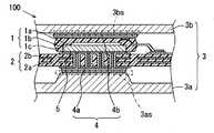
図1は、本発明の電子部品の放熱構造100を示す断面模式図である。 FIG. 1 is a schematic cross-sectional view showing a
図1において、符号1は発熱を伴う電子部品である。図1の電子部品1は、発熱を伴う半導体チップ1aが台座1b上に搭載され、樹脂1cでモールドされたものである。符号2は、電子部品1を搭載する回路基板である。図1の回路基板2は、絶縁母材2aに導体パターン2bが多層に形成された多層回路基板である。電子部品1は、半田5により台座1bが回路基板2の表面にある導体パターンに接続されて、回路基板2に搭載されている。符号3は、回路基板2を収容する熱伝導性のあるケースである。図1のケース3は、下側ケース3aと上側ケース3bで構成されている。符号4は、電子部品1の発生する熱をケース3に伝導するグリースである。図1では、グリース4aが下側ケース3aと回路基板2の間に介在しており、グリース4bが上側ケース3bと電子部品1の間に介在している。In FIG. 1,
図1に示す電子部品の放熱構造100においては、図中の一点差線で囲ったケースにおけるグリースとの接触面3as,3bsの表面状態が、次の図2に示す試験で得られた、グリースの流動を抑制できる所定範囲に規定される。 In the
図2は、ケースにおけるグリースとの接触面の表面状態因子として、表面自由エネルギーと表面粗さRz(JIS B 0601)について、グリースの流動を振動試験により評価した結果である。 FIG. 2 is a result of evaluating the flow of grease by a vibration test with respect to surface free energy and surface roughness Rz (JIS B 0601) as surface condition factors of the contact surface with the grease in the case.
図2の試験に供したグリースは、シリコーンをベース成分とし、フィラーとして酸化亜鉛(ZnO)が60wt%以上90wt%以下の範囲で充填され、200Pa・sec以上500Pa・sec以下の粘度を有するグリースである。このグリースは、高い熱伝導性能と好適な粘度を有しており、長期間に渡って熱伝導性能が劣化することがない。尚、図2の評価試験は、20Gの振動を96時間印加した後のグリースの移動量を評価したものである。また、試験に供したグリースの粘度は、スパイラル粘度計(マルコム社製)を用い、回転数10rpm、温度25℃の条件で測定した。 The grease used for the test in FIG. 2 is a grease having a viscosity of 200 Pa · sec or more and 500 Pa · sec or less filled with zinc oxide (ZnO) as a filler in a range of 60 wt% or more and 90 wt% or less. is there. This grease has a high thermal conductivity and a suitable viscosity, and the thermal conductivity does not deteriorate over a long period of time. Note that the evaluation test of FIG. 2 is an evaluation of the amount of grease movement after applying 20 G vibration for 96 hours. Moreover, the viscosity of the grease used for the test was measured using a spiral viscometer (manufactured by Malcolm) under the conditions of a rotation speed of 10 rpm and a temperature of 25 ° C.
試料3〜試料5のアルミニウム圧延材は、熱伝導率が高く、放熱性能に優れるため、回路基板を収容するケース材として一般的に用いられている。試料3〜試料5のアルミニウム圧延材は、特別な表面処理を施していない、加工したままの状態のもので、31.0〜37.1mN/mの表面自由エネルギーと、0.79〜2.51μmの表面粗さRzを有している。試料6のアルミニウムダイキャスト材も、回路基板を収容するケース材として一般的に用いられる。試料6のアルミニウムダイキャスト材は、34.6mN/mの表面自由エネルギーと、4.25μmの表面粗さRzを有している。 The aluminum rolled material of
鉄は、一般的にアルミニウムより大きな表面自由エネルギーを有しており、試料7の鉄圧延材は、40.5mN/mの表面自由エネルギーと、2.94μmの表面粗さRzを有している。樹脂材料は、一般的に金属材料より小さな表面自由エネルギーを有しており、試料1のテフロン(登録商標)は、19.3mN/mの表面自由エネルギーと、1.42μmの表面粗さRzを有している。また、試料2のセロハン(商品名)は、25.1mN/mの表面自由エネルギーと、0.75μmの表面粗さRzを有している。 Iron generally has a larger surface free energy than aluminum, and the iron rolled material of Sample 7 has a surface free energy of 40.5 mN / m and a surface roughness Rz of 2.94 μm. . The resin material generally has a surface free energy smaller than that of the metal material, and the Teflon (registered trademark) of
図2の評価結果に示すように、表面自由エネルギーが低い試料1のテフロン(登録商標)と試料2のセロハン(商品名)を用いた試料では、20G・96時間の振動試験評価で、グリースが流動した。また、アルミニウム圧延材を用いた試料3〜5では、表面粗さRzの小さい試料3と試料4でグリースが流動した。一方、アルミニウム圧延材を用いた表面粗さRzの大きい試料5と、アルミニウムダイキャスト材を用いた試料6および鉄圧延材を用いた試料7については、グリースの流動が抑制された。 As shown in the evaluation results of FIG. 2, in the sample using Teflon (registered trademark) of
図2の結果を分析すると、試料1〜試料4の結果より、グリースの流動を抑制するためには、接触面3as,3bsの表面自由エネルギーが20mN/m以上であり、接触面3as,3bsの表面粗さRzが1.0μm以上であることが必要である。また、試料5〜試料7の結果より、グリースの流動を抑制するためには、接触面3as,3bsの表面自由エネルギーが34mN/m以上で、接触面3as,3bsの表面粗さRzが2.5μm以上であることが好ましい。 When the result of FIG. 2 is analyzed, the surface free energy of the contact surfaces 3as, 3bs is 20 mN / m or more and the contact surfaces 3as, 3bs are less The surface roughness Rz needs to be 1.0 μm or more. Further, from the results of
接触面3as,3bsの表面自由エネルギーが20mN/m以上、好ましくは34mN/m以上の場合には、接触面3as,3bsのグリース付着力が大きいため、この表面自由エネルギーによるグリース付着力によって、グリースの流動が抑制されると考えられる。また、接触面3as,3bsの表面粗さRzも1.0μm以上、好ましくは2.5μm以上の場合には、接触面3as,3bsの凹凸がグリースの流動の抵抗となり、この表面粗さRzで表される接触面3as,3bsの凹凸によっても、グリースの流動が抑制されると考えられる。従って、図2の結果は、上記2つの効果が相まって、グリースの流動が抑制されていると考えられる。 When the surface free energy of the contact surfaces 3as, 3bs is 20 mN / m or more, preferably 34 mN / m or more, the grease adhesion force of the contact surfaces 3as, 3bs is large. It is thought that the flow of is suppressed. In addition, when the surface roughness Rz of the contact surfaces 3as and 3bs is also 1.0 μm or more, preferably 2.5 μm or more, the unevenness of the contact surfaces 3as and 3bs becomes the resistance to grease flow, and the surface roughness Rz It is considered that the flow of grease is also suppressed by the unevenness of the contact surfaces 3as and 3bs represented. Therefore, the result of FIG. 2 is considered that the flow of grease is suppressed by the combination of the above two effects.
以上の結果より、接触面3as,3bsの表面自由エネルギーを20mN/m以上、好ましくは34mN/m以上とし、表面粗さRzを1.0μm以上、好ましくは2.5μm以上とした図1の電子部品の放熱構造100は、グリースの流動が抑制され、初期の放熱性能を長期間に渡って維持することができる。従って、図1の電子部品の放熱構造100を、長期間に渡って放熱性能が劣化しない電子部品の放熱構造とすることができる。 From the above results, the surface free energy of the contact surfaces 3as and 3bs is 20 mN / m or more, preferably 34 mN / m or more, and the surface roughness Rz is 1.0 μm or more, preferably 2.5 μm or more. In the
次に、車載環境のように回路基板が様々な向きに搭載され、温度変化の大きい環境に晒される場合に好適な電子部品の放熱構造について説明する。 Next, a description will be given of a heat dissipation structure for an electronic component that is suitable when a circuit board is mounted in various directions as in an in-vehicle environment and is exposed to an environment with a large temperature change.
温度変化の大きい環境では、冷熱サイクルによって、グリースが重力方向へ向かって移動していく現象が見られる。 In an environment where the temperature change is large, a phenomenon in which the grease moves toward the direction of gravity due to the cooling / heating cycle is observed.
図3(a)〜(c)は、冷熱サイクルによるグリースの移動のメカニズムを検討するため、グリースが熱膨張(25→105℃)する際、グリースが動き出す直前の応力をFEMで解析した結果である。図3(a)は、解析に用いた回路基板2、ケース3およびグリース4の配置を示すモデル図である。図3(b)は、解析で得られたせん断応力の分布図である。図3(c)は、図3(b)において一点鎖線で囲ったA部のせん断応力をグラフ化して示した図である。 3 (a) to 3 (c) show the results of FEM analysis of the stress immediately before the grease starts to move when the grease undergoes thermal expansion (25 → 105 ° C) in order to study the mechanism of grease movement due to the thermal cycle. is there. FIG. 3A is a model diagram showing the arrangement of the
図3(b)の結果に見られるように、グリース4が熱膨張する場合には、ケース3もしくは回路基板2との接触面におけるグリース4の端部に、応力集中が起きている。図3(c)に示すように、応力集中は接触面から25μm程度の高さの範囲におさまっている。従って、グリースの移動のメカニズムは、次のように考えられる。すなわち、熱膨張率によりグリース4が膨らんだ際、端部に応力集中があり、グリース4の移動に抗する抵抗力の限界を越えた場合にグリース4が移動する。温度が下がった場合にはグリース4が元の位置までもどらず、その結果、冷熱サイクルの進行とともにグリース4が移動していく。特に、ケース3もしくは回路基板2が、重力方向に対して傾いた状態で保持される場合には、この現象が顕著となり、90°に傾いた状態で保持される場合に最大となる。 As can be seen from the result of FIG. 3B, when the
以上に示したように、グリース4が熱膨張する場合には、ケース3もしくは回路基板2との接触面におけるグリース4の端部に応力集中が起きる。この応力集中に対して、高い段がケース3もしくは回路基板2にあると、グリース4はこれを乗り越えて移動することができないと考えられる。従って、ケース3もしくは回路基板2の表面において、グリース4が介在する場所の周りに、表面からの高さが25μm以上の段を形成することで、グリース4の熱膨張による横方向へのはみ出し、および移動を抑制することができる。 As described above, when the
図4(a)〜(c)は、上記の冷熱サイクルによるグリースの移動のメカニズム検討結果をもとに、ケース30に段30dを形成して、グリース4の移動を防止する構造を試験した結果である。 4 (a) to 4 (c) show the results of testing a structure in which a
図4(a)は、冷熱サイクル(−40℃,125℃間)試験に用いた回路基板2、ケース30およびグリース4の配置を示すモデル図である。回路基板2は一般的なプリント基板であり、ケース30はアルミニウムダイキャスト材である。グリース4の塗布量は、0.2mlとしている。 FIG. 4A is a model diagram showing the arrangement of the
図4(b)は、冷熱サイクル後のグリース4のズレ距離を表に示した図であり、図4(c)は、図4(b)の結果をグラフ化して示した図である。 FIG. 4B is a table showing the deviation distance of the
図4(c)に示したように、−40℃と125℃の間の冷熱サイクル試験において、50サイクルでは、段30dを形成しなくても(h=0mm)、グリース4のズレはほとんどみられない。しかしながら、300サイクルでは、段30dがないとグリース4のズレ距離は8mm程度になって、顕著なズレがみられる。一方、0.1mm以上の高さの段30dを形成した試料では、300サイクルにおいても、グリース4のズレが確実に抑制されている。 As shown in FIG. 4 (c), in the thermal cycle test between −40 ° C. and 125 ° C., in 50 cycles, even if the
上記の段30dによるグリース4の移動の抑制は、25μm程度の高さでも効果を発揮するため、ケース30もしくは回路基板4のどのような場所に設けても、電子部品の実装の邪魔になることはない。従って、設計自由度が低下することもない。 Since the suppression of the movement of the
図5(a)〜(d)は、ケースの表面に形成される上記の段の様々な形態を示す平面図である。 FIGS. 5A to 5D are plan views showing various forms of the steps formed on the surface of the case.
図5(a)は、ケース31が、重力方向に対して傾いた状態で保持される場合に好適な段31dの形態である。図5(a)のケース31では、段31dが、表面における重力成分方向を横切るようにして、グリース4が介在する場所の下側に形成されている。 FIG. 5A shows a form of a
ケースが重力方向に対して傾いた状態で保持される場合には、ケースの表面における重力成分方向が、グリースの移動の容易方向となる。従って、ケース31のように、表面における重力成分方向を横切るようにして、グリース4が介在する場所の下側に段31dを形成することで、傾いた状態で保持する場合にも、グリース4の移動を確実に抑制することができる。 When the case is held in a state of being inclined with respect to the direction of gravity, the direction of gravity component on the surface of the case is an easy direction for grease movement. Therefore, as in the
図5(b)のケース32では、段32dが、ケース32の表面において、縞状に形成されている。これにより、グリース4の移動を、より広範囲で、より確実に抑制することができる。 In the
図5(c)のケース33では、段33dが、ケース33の表面において、格子状に形成されている。また、図5(d)のケース34では、段34dが、ケース34の表面において、亀甲状に形成されている。 In the case 33 of FIG. 5C, the
図5(c)のケース33と図5(d)のケース34の場合には、ケース33,34の重力方向に対する保持方向が未定である場合や、様々な方向に保持される可能性がある場合においても、グリース4の移動を確実に抑制することができる。 In the case 33 of FIG. 5C and the
尚、図5(a)〜(d)はケース31〜34に段31d〜34dを形成する場合について示してあるが、回路基板に段を形成する場合も同様である。 5A to 5D show the case where the
図6(a)〜(c)は、図3(a)〜(c)の冷熱サイクルによるグリースの移動のメカニズム検討結果をもとに、グリース4の移動を防止する別の構造を試験した結果である。 6A to 6C show the results of testing another structure for preventing the movement of the
図6(a)は、冷熱サイクル(−40℃,125℃間)試験に用いた回路基板2、ケース35およびグリース4の配置を示すモデル図である。尚、図4(a)の試験と同様に、試験に用いた回路基板2は一般的なプリント基板であり、ケース35はアルミニウムダイキャスト材である。グリース4の塗布量は、0.2mlとしている。 FIG. 6A is a model diagram showing the arrangement of the
図6(a)の構造は、グリース4が介在する場所の周りにおけるケース35と回路基板2の表面が平板状であり、ケース35の表面と回路基板2の表面が、互いに傾いた状態で配置される構造である。ケース35の表面と回路基板2の表面が互いに傾いた状態で配置される場合には、一方で両者の間の幅が狭くなり、他方で両者の間の幅が広くなる。従って、グリース4が熱膨張して広がる場合、一方ではグリース4の厚さが薄くなり、他方ではグリース4の厚さが厚くなる。一般に、流体の抵抗は、流路が狭くなるほど大きくなる。従って、グリース4は、ケース35と回路基板2の間の幅が広くなる方向に膨張し、狭くなる方向への移動が抑制される。従って、図6(a)に示すように、ケース35もしくは回路基板2が、重力方向に対して傾いた状態で保持される場合に好適で、グリース4を挟む、ケース35の表面と回路基板2の表面で構成される空間の幅が、ケース35の表面もしくは回路基板2の表面における重力成分方向に向かって狭くなるようにすることで、傾いた状態で保持する場合にも、グリース4の移動を確実に抑制することができると考えられる。 In the structure of FIG. 6A, the surface of the
図6(b)は、冷熱サイクル後のグリース4のズレ距離を表に示した図であり、図6(c)は、図6(b)の結果をグラフ化して示した図である。 FIG. 6B is a table showing the deviation distance of the
図6(c)に示したように、−40℃と125℃の間の冷熱サイクル試験において、 ケース35の表面と回路基板2の表面を互いに1°以上傾いた状態で配置したものについては、300サイクルにおいて、グリース4の移動が確実に抑制されている。また、さらにサイクル数を増した試験によれば、グリース4の移動の抑制には、ケース35の表面と回路基板2の表面を互いに3°以上傾いた状態で配置することが特に好ましい。 As shown in FIG. 6C, in the thermal cycle test between −40 ° C. and 125 ° C., the surface of the
上記のケース35の表面と回路基板2の表面が互いに傾いた状態で配置される放熱構造についても、グリース4が介在する場所の周りにおけるケース35と回路基板2の表面は平板状であり、電子部品の実装の邪魔になることはない。従って、設計自由度が低下することもない。 Also in the heat dissipation structure in which the surface of the
図4(a)〜(c)および図6(a)〜(c)の試験においては、ケース30,35の表面と回路基板2の表面の間に介在するグリース4の厚さを1mmに設定して、冷熱サイクル試験を行っている。 In the tests of FIGS. 4A to 4C and FIGS. 6A to 6C, the thickness of the
ケースと回路基板の間にグリースを介在させるに際して、ケースの表面と回路基板の表面の間に介在するグリースの厚さは、10mm以下であることが好ましい。これにより、図4(a)〜(c)に示したケースもしくは回路基板の表面において形成される段の効果、もしくは図6(a)〜(c)に示したケースの表面と回路基板の表面を互いに傾いた状態で配置する場合の効果を、確実に発揮させることができる。 When the grease is interposed between the case and the circuit board, the thickness of the grease interposed between the case surface and the circuit board surface is preferably 10 mm or less. Thereby, the effect of the step formed on the surface of the case or the circuit board shown in FIGS. 4A to 4C, or the surface of the case and the surface of the circuit board shown in FIGS. 6A to 6C. It is possible to reliably exhibit the effect of arranging them in a tilted state.
(他の実施形態)
図2の評価試験は、シリコーンをベース成分とし、フィラーとして酸化亜鉛(ZnO)が60wt%以上90wt%以下の範囲で充填され、200Pa・sec以上500Pa・sec以下の粘度を有するグリースで行った。これに限らず、上記表面自由エネルギーと表面粗さRzを有する本発明の電子部品の放熱構造では、50Pa・sec以上2000Pa・sec以下の粘度を有する一般的なグリースを用いても、同様の効果を得ることができる。上記粘度範囲にあるグリースは、放熱部への塗布が容易であると共に、上記ケースと共に用いることで長期に渡って流動が抑制できる。(Other embodiments)
The evaluation test in FIG. 2 was performed with grease having silicone as a base component and zinc oxide (ZnO) as a filler in a range of 60 wt% to 90 wt% and having a viscosity of 200 Pa · sec to 500 Pa · sec. The heat dissipation structure of the electronic component of the present invention having the surface free energy and the surface roughness Rz is not limited to this, and the same effect can be obtained even when a general grease having a viscosity of 50 Pa · sec to 2000 Pa · sec is used. Can be obtained. The grease in the above viscosity range can be easily applied to the heat radiating portion, and can be prevented from flowing for a long period of time when used together with the case.
図4(a)〜(c)および図6(a)〜(c)の試験においては、ケース30,35もしくは回路基板2が重力方向に対して90°傾いた状態で保持される場合について示したが、任意の角度に傾いた状態で保持される場合についても同様であることはいうまでもない。 In the tests of FIGS. 4A to 4C and FIGS. 6A to 6C,
また、図4(a)〜(c)および図6(a)〜(c)の試験は、図2に示したアルミニウムダイキャスト材からなるケースを用いた試験であった。しかしながら、図3〜図6で説明した発明の効果は上記材料のケースに限らず、グリースとの接触面における表面自由エネルギーと表面粗さが任意の値を持つケースに対して適用可能で、同様の効果が発揮されることはいうまでもない。 Moreover, the test of Fig.4 (a)-(c) and Fig.6 (a)-(c) was a test using the case which consists of an aluminum die-cast material shown in FIG. However, the effects of the invention described with reference to FIGS. 3 to 6 are not limited to the case of the above material, but can be applied to a case where the surface free energy and the surface roughness at the contact surface with the grease have arbitrary values. Needless to say, the effect of is exhibited.
1 電子部品
2 回路基板
3,3a,3b,30〜35 ケース
3as,3bs ケースにおけるグリースとの接触面
30d〜34d 段
4,4a,4b グリース
100 放熱構造DESCRIPTION OF
Claims (9)
Translated fromJapanese前記グリースが介在する場所の周りにおける前記ケースと回路基板の表面が平板状であり、
前記ケースの表面と回路基板の表面が、互いに傾いた状態で配置されてなり、
前記ケースもしくは回路基板の一方が、重力方向に対して傾いた状態で保持され、
前記ケースもしくは回路基板のもう一方が、重力方向に対して平行または傾いた状態で保持されてなり、
前記グリースを挟む、前記ケースの表面と回路基板の表面で構成される空間の幅が、重力方向に向かって、狭くなることを特徴とする電子部品の放熱構造。An electronic component that generates heat; a circuit board on which the electronic component is mounted; a thermally conductive case that houses the circuit board; andat least the gap between the case and the circuit board. A heat dissipation structure for an electronic component having grease that conducts generated heat to the case,
The surface of the case and the circuit board around the place where the grease is interposed is plate-shaped,
The surface of the case and the surface of the circuit board are arranged in an inclined state,
One of the case or the circuit board is held in a state inclined with respect to the direction of gravity,
The other of the case or the circuit board is held in a state parallel or inclined with respect to the direction of gravity,
A heat dissipation structure for an electronic component, characterized in that a space formed by the surface of the case and the surface of the circuit board sandwiching the grease becomes narrower in the direction of gravity.
Priority Applications (3)
| Application Number | Priority Date | Filing Date | Title |
|---|---|---|---|
| JP2004046826AJP4457694B2 (en) | 2003-05-19 | 2004-02-23 | Heat dissipation structure for electronic components |
| US10/846,871US7057891B2 (en) | 2003-05-19 | 2004-05-14 | Heat dissipation structure |
| DE102004024616ADE102004024616A1 (en) | 2003-05-19 | 2004-05-18 | heat dissipation |
Applications Claiming Priority (2)
| Application Number | Priority Date | Filing Date | Title |
|---|---|---|---|
| JP2003141080 | 2003-05-19 | ||
| JP2004046826AJP4457694B2 (en) | 2003-05-19 | 2004-02-23 | Heat dissipation structure for electronic components |
Publications (2)
| Publication Number | Publication Date |
|---|---|
| JP2005005671A JP2005005671A (en) | 2005-01-06 |
| JP4457694B2true JP4457694B2 (en) | 2010-04-28 |
Family
ID=33455517
Family Applications (1)
| Application Number | Title | Priority Date | Filing Date |
|---|---|---|---|
| JP2004046826AExpired - Fee RelatedJP4457694B2 (en) | 2003-05-19 | 2004-02-23 | Heat dissipation structure for electronic components |
Country Status (3)
| Country | Link |
|---|---|
| US (1) | US7057891B2 (en) |
| JP (1) | JP4457694B2 (en) |
| DE (1) | DE102004024616A1 (en) |
Families Citing this family (31)
| Publication number | Priority date | Publication date | Assignee | Title |
|---|---|---|---|---|
| JP2003289191A (en)* | 2002-03-28 | 2003-10-10 | Denso Corp | Electronic control device |
| US7586189B2 (en)* | 2004-08-30 | 2009-09-08 | Denso Corporation | Heat dissipation structure accommodated in electronic control device |
| TWI388042B (en)* | 2004-11-04 | 2013-03-01 | Taiwan Semiconductor Mfg | Integrated circuit nanotube-based substrate |
| US7443685B2 (en)* | 2005-02-03 | 2008-10-28 | Fujitsu Limited | Conductive heat transfer for electrical devices from the solder side and component side of a circuit card assembly |
| DE102005049872B4 (en)* | 2005-10-18 | 2010-09-23 | Continental Automotive Gmbh | IC component with cooling arrangement |
| JP4525615B2 (en)* | 2006-03-01 | 2010-08-18 | 株式会社デンソー | Power converter |
| DE102006013017B4 (en) | 2006-03-20 | 2014-11-06 | R. Stahl Schaltgeräte GmbH | Housing with thermal bridge |
| US20080080142A1 (en)* | 2006-09-28 | 2008-04-03 | Mediatek Inc. | Electronic devices with enhanced heat spreading |
| EP1947921B1 (en)* | 2007-01-17 | 2009-10-21 | MEN Mikro Elektronik GmbH | Electronic module |
| US7808788B2 (en)* | 2007-06-29 | 2010-10-05 | Delphi Technologies, Inc. | Multi-layer electrically isolated thermal conduction structure for a circuit board assembly |
| DE102008039921B4 (en)* | 2008-08-27 | 2021-06-10 | Vitesco Technologies GmbH | Method of manufacturing an electronic device with a discrete component |
| JP2010245174A (en)* | 2009-04-02 | 2010-10-28 | Denso Corp | Electronic control unit and method of manufacturing the same |
| US20100251536A1 (en)* | 2009-04-06 | 2010-10-07 | Moxa Inc. | Heat-dissipating structure on case of industrial computer and manufacturing method thereof |
| JP2010287796A (en)* | 2009-06-12 | 2010-12-24 | Sony Corp | Electronic equipment |
| US9101082B1 (en) | 2010-05-03 | 2015-08-04 | Sunpower Corporation | Junction box thermal management |
| DE102010030525A1 (en)* | 2010-06-25 | 2011-12-29 | Zf Friedrichshafen Ag | Electronic control module |
| JP2012142391A (en) | 2010-12-28 | 2012-07-26 | Sumitomo Electric Ind Ltd | Electric apparatus, and method of manufacturing electric apparatus |
| WO2012090546A1 (en)* | 2010-12-28 | 2012-07-05 | 住友電気工業株式会社 | Electrical appliance, method for manufacturing electrical appliance, and wireless communication device |
| DE102011088256A1 (en)* | 2011-12-12 | 2013-06-13 | Zf Friedrichshafen Ag | Multilayer printed circuit board and arrangement with such |
| FR2987170A1 (en) | 2012-02-17 | 2013-08-23 | St Microelectronics Grenoble 2 | ELECTRONIC HOUSING AND DEVICE |
| TW201410127A (en)* | 2012-08-30 | 2014-03-01 | Hon Hai Prec Ind Co Ltd | Electronic device |
| JP5803856B2 (en)* | 2012-09-06 | 2015-11-04 | 株式会社デンソー | Electronic control unit |
| JP2014203998A (en)* | 2013-04-05 | 2014-10-27 | 日立オートモティブシステムズ株式会社 | In-vehicle electronic controller |
| CN107079578A (en)* | 2014-09-24 | 2017-08-18 | Hiq太阳能股份有限公司 | Transistor heat management and EMI rwan management solution RWANs for fast edge rates environment |
| EP3220418B1 (en) | 2016-03-18 | 2021-03-03 | Mitsubishi Electric R&D Centre Europe B.V. | Power module comprising a heat sink and a substrate to which a power die is attached and method for manufacturing the power module |
| US10420255B2 (en)* | 2016-09-14 | 2019-09-17 | Jtekt Corporation | Electronic control device |
| US11393737B2 (en)* | 2017-05-22 | 2022-07-19 | Sony Interactive Entertainment Inc. | Electronic equipment |
| JP7522752B2 (en)* | 2019-09-25 | 2024-07-25 | デンカ株式会社 | HEAT DISLIPPER SHEET, HEAT DISLIPPER SHEET LAMINATE, STRUCTURE, AND METHOD FOR HEAT DISLIPPER TREATMENT OF HEAT-HEAVY ELEMENT |
| CN114430860A (en)* | 2019-09-26 | 2022-05-03 | 电化株式会社 | Heat sink |
| DE102019215503A1 (en)* | 2019-10-10 | 2021-04-15 | Vitesco Technologies GmbH | Power semiconductor component and method for manufacturing a power semiconductor component |
| US12156381B2 (en)* | 2022-11-10 | 2024-11-26 | Techway Industrial Co., Ltd. | Heat dissipation device of electronic equipment |
Family Cites Families (15)
| Publication number | Priority date | Publication date | Assignee | Title |
|---|---|---|---|---|
| JPS5740965A (en)* | 1980-08-26 | 1982-03-06 | Nec Corp | Hybrid integrated circuit device |
| JP2580348B2 (en)* | 1989-11-20 | 1997-02-12 | 信越化学工業 株式会社 | Grease composition for heat radiation |
| JP2748778B2 (en) | 1992-05-29 | 1998-05-13 | 日本電気株式会社 | Hybrid integrated circuit device |
| US5396403A (en)* | 1993-07-06 | 1995-03-07 | Hewlett-Packard Company | Heat sink assembly with thermally-conductive plate for a plurality of integrated circuits on a substrate |
| JP3044172B2 (en)* | 1993-10-12 | 2000-05-22 | 呉羽化学工業株式会社 | Transfer sheet |
| JPH0955459A (en)* | 1995-06-06 | 1997-02-25 | Seiko Epson Corp | Semiconductor device |
| US6143076A (en)* | 1996-06-21 | 2000-11-07 | Thermalloy Inc. | Applicator head |
| JPH11135691A (en)* | 1997-10-31 | 1999-05-21 | Hitachi Ltd | Electronic circuit device |
| WO2001040357A1 (en)* | 1999-12-03 | 2001-06-07 | Toray Industries, Inc. | Biaxially stretched polyester film for forming |
| JP3920048B2 (en) | 2000-07-13 | 2007-05-30 | 日本特殊陶業株式会社 | Through-hole filling paste |
| JP2002083912A (en) | 2000-09-08 | 2002-03-22 | Denso Corp | Electronic component radiation structure |
| JP3690729B2 (en) | 2000-09-11 | 2005-08-31 | インターナショナル・ビジネス・マシーンズ・コーポレーション | Electric circuit device and computer |
| JP2002217346A (en) | 2001-01-19 | 2002-08-02 | Toyota Motor Corp | Electronic element chip module |
| JP2003027080A (en) | 2001-07-11 | 2003-01-29 | Hitachi Ltd | Thermal conductive grease, mounting method thereof, cooling method of electronic component, electronic device and information processing device |
| JP2003086747A (en)* | 2001-09-10 | 2003-03-20 | Hitachi Ltd | Insulated circuit board, method of manufacturing the same, and semiconductor power device using the same |
- 2004
- 2004-02-23JPJP2004046826Apatent/JP4457694B2/ennot_activeExpired - Fee Related
- 2004-05-14USUS10/846,871patent/US7057891B2/ennot_activeExpired - Lifetime
- 2004-05-18DEDE102004024616Apatent/DE102004024616A1/ennot_activeWithdrawn
Also Published As
| Publication number | Publication date |
|---|---|
| US7057891B2 (en) | 2006-06-06 |
| DE102004024616A1 (en) | 2004-12-16 |
| US20040233642A1 (en) | 2004-11-25 |
| JP2005005671A (en) | 2005-01-06 |
Similar Documents
| Publication | Publication Date | Title |
|---|---|---|
| JP4457694B2 (en) | Heat dissipation structure for electronic components | |
| US7755895B2 (en) | Heat sink, an electronic component package, and a method of manufacturing a heat sink | |
| KR101017452B1 (en) | Semiconductor package | |
| US20020015288A1 (en) | High performance thermal/mechanical interface for fixed-gap references for high heat flux and power semiconductor applications | |
| WO2006009267A1 (en) | Heat pipe heat sink | |
| JP2003332505A (en) | Cooling structure and heat transfer member | |
| JP2002305271A (en) | Heat radiating structure of electronic component and heat radiating sheet used therefor | |
| US8446727B2 (en) | Electronic component | |
| JP2010129877A (en) | Electronic component module | |
| JP7176318B2 (en) | Electrical equipment and radiators | |
| JP2006294754A (en) | Heat dissipation structure of electronic apparatus | |
| JP4846434B2 (en) | Cement resistor | |
| JP6055698B2 (en) | Electronic control device, heat dissipation structure thereof, and electronic device equipped with the electronic control device | |
| JP5155914B2 (en) | Controller unit | |
| JP5157266B2 (en) | Radiator and method of manufacturing radiator | |
| JP2007532002A (en) | Thermal diffuser structure, integrated circuit, method of forming thermal diffuser structure, and method of forming integrated circuit | |
| JP4289252B2 (en) | Heat dissipation structure for electronic devices | |
| JP6650978B2 (en) | Electronic control unit | |
| JP7602009B2 (en) | In-vehicle electronic devices | |
| JP5003730B2 (en) | Electronic equipment | |
| JPH11163564A (en) | Electronic device and method of manufacturing electronic device | |
| JP4452888B2 (en) | Electronic circuit equipment | |
| JP2006196593A (en) | Semiconductor device and heat sink | |
| JP6551566B1 (en) | Heat dissipation structure of electronic parts | |
| JP2007250772A (en) | Electronic control apparatus |
Legal Events
| Date | Code | Title | Description |
|---|---|---|---|
| A621 | Written request for application examination | Free format text:JAPANESE INTERMEDIATE CODE: A621 Effective date:20060428 | |
| A977 | Report on retrieval | Free format text:JAPANESE INTERMEDIATE CODE: A971007 Effective date:20061004 | |
| A131 | Notification of reasons for refusal | Free format text:JAPANESE INTERMEDIATE CODE: A131 Effective date:20080212 | |
| A521 | Request for written amendment filed | Free format text:JAPANESE INTERMEDIATE CODE: A523 Effective date:20080410 | |
| A131 | Notification of reasons for refusal | Free format text:JAPANESE INTERMEDIATE CODE: A131 Effective date:20090317 | |
| A521 | Request for written amendment filed | Free format text:JAPANESE INTERMEDIATE CODE: A523 Effective date:20090421 | |
| TRDD | Decision of grant or rejection written | ||
| A01 | Written decision to grant a patent or to grant a registration (utility model) | Free format text:JAPANESE INTERMEDIATE CODE: A01 Effective date:20100119 | |
| A01 | Written decision to grant a patent or to grant a registration (utility model) | Free format text:JAPANESE INTERMEDIATE CODE: A01 | |
| A61 | First payment of annual fees (during grant procedure) | Free format text:JAPANESE INTERMEDIATE CODE: A61 Effective date:20100201 | |
| R151 | Written notification of patent or utility model registration | Ref document number:4457694 Country of ref document:JP Free format text:JAPANESE INTERMEDIATE CODE: R151 | |
| FPAY | Renewal fee payment (event date is renewal date of database) | Free format text:PAYMENT UNTIL: 20130219 Year of fee payment:3 | |
| FPAY | Renewal fee payment (event date is renewal date of database) | Free format text:PAYMENT UNTIL: 20140219 Year of fee payment:4 | |
| R250 | Receipt of annual fees | Free format text:JAPANESE INTERMEDIATE CODE: R250 | |
| R250 | Receipt of annual fees | Free format text:JAPANESE INTERMEDIATE CODE: R250 | |
| R250 | Receipt of annual fees | Free format text:JAPANESE INTERMEDIATE CODE: R250 | |
| R250 | Receipt of annual fees | Free format text:JAPANESE INTERMEDIATE CODE: R250 | |
| R250 | Receipt of annual fees | Free format text:JAPANESE INTERMEDIATE CODE: R250 | |
| R250 | Receipt of annual fees | Free format text:JAPANESE INTERMEDIATE CODE: R250 | |
| R250 | Receipt of annual fees | Free format text:JAPANESE INTERMEDIATE CODE: R250 | |
| R250 | Receipt of annual fees | Free format text:JAPANESE INTERMEDIATE CODE: R250 | |
| LAPS | Cancellation because of no payment of annual fees |