JP4454943B2 - Driving method of light emitting device - Google Patents
Driving method of light emitting deviceDownload PDFInfo
- Publication number
- JP4454943B2 JP4454943B2JP2003052746AJP2003052746AJP4454943B2JP 4454943 B2JP4454943 B2JP 4454943B2JP 2003052746 AJP2003052746 AJP 2003052746AJP 2003052746 AJP2003052746 AJP 2003052746AJP 4454943 B2JP4454943 B2JP 4454943B2
- Authority
- JP
- Japan
- Prior art keywords
- thin film
- period
- film transistor
- light emitting
- driving
- Prior art date
- Legal status (The legal status is an assumption and is not a legal conclusion. Google has not performed a legal analysis and makes no representation as to the accuracy of the status listed.)
- Expired - Fee Related
Links
- 238000000034methodMethods0.000titleclaimsdescription31
- 239000010409thin filmSubstances0.000claimsdescription39
- 238000005401electroluminescenceMethods0.000description70
- 238000010586diagramMethods0.000description9
- 239000000758substrateSubstances0.000description7
- 230000006866deteriorationEffects0.000description6
- 238000002347injectionMethods0.000description5
- 239000007924injectionSubstances0.000description5
- 239000011159matrix materialSubstances0.000description5
- 238000012360testing methodMethods0.000description5
- 239000010408filmSubstances0.000description4
- 230000005525hole transportEffects0.000description4
- 239000003990capacitorSubstances0.000description3
- 230000015556catabolic processEffects0.000description3
- 230000007423decreaseEffects0.000description3
- 230000007274generation of a signal involved in cell-cell signalingEffects0.000description3
- 239000004973liquid crystal related substanceSubstances0.000description3
- 239000000463materialSubstances0.000description3
- 238000005070samplingMethods0.000description3
- 102100027300Extracellular serine/threonine protein kinase FAM20CHuman genes0.000description2
- 101000937709Homo sapiens Extracellular serine/threonine protein kinase FAM20CProteins0.000description2
- 150000001875compoundsChemical class0.000description2
- 239000004020conductorSubstances0.000description2
- 230000000694effectsEffects0.000description2
- 239000007787solidSubstances0.000description2
- 208000019901Anxiety diseaseDiseases0.000description1
- 230000036506anxietyEffects0.000description1
- 239000000969carrierSubstances0.000description1
- 238000006243chemical reactionMethods0.000description1
- 239000003086colorantSubstances0.000description1
- 238000004891communicationMethods0.000description1
- 229920001940conductive polymerPolymers0.000description1
- 238000006731degradation reactionMethods0.000description1
- 238000007599dischargingMethods0.000description1
- 239000012535impuritySubstances0.000description1
- 238000005259measurementMethods0.000description1
- 239000000049pigmentSubstances0.000description1
- 229920000642polymerPolymers0.000description1
- 238000012545processingMethods0.000description1
- 238000005215recombinationMethods0.000description1
- 230000006798recombinationEffects0.000description1
- 238000012827research and developmentMethods0.000description1
- 230000004044responseEffects0.000description1
Images


Landscapes
- Control Of Indicators Other Than Cathode Ray Tubes (AREA)
- Control Of El Displays (AREA)
- Electroluminescent Light Sources (AREA)
Description
Translated fromJapanese【0001】
【発明の属する技術分野】
本発明は、発光素子および、薄膜トランジスタ(以下TFTと表記)を基板上に作り込んで形成された発光装置の駆動方法に関する。また発光装置を表示部に用いた電子機器に関する。
【0002】
なお、本明細書中では、発光素子の代表的なものとしてエレクトロルミネッセンス(Electro Luminescence:EL)素子を例とし、またEL素子とは、一重項励起子からの発光(蛍光)を利用するものと、三重項励起子からの発光(燐光)を利用するものの両方を示すものとする。
【0003】
【従来の技術】
近年、自発光型素子として、EL素子を有した発光装置の開発が活発化している。発光装置は、液晶表示装置と異なり自発光型である。EL素子は一対の電極(陽極と陰極)間にEL層が挟まれた構造となっているが、EL層は通常、積層構造となっている。代表的には、「正孔輸送層/発光層/電子輸送層」という積層構造が挙げられる。この構造は非常に発光効率が高く、現在、研究開発が進められているEL表示装置はほとんどこの構造を採用している。
【0004】
また他にも、陽極上に正孔注入層/正孔輸送層/発光層/電子輸送層の順に積層する構造、または正孔注入層/正孔輸送層/発光層/電子輸送層/電子注入層の順に積層する構造でも良い。発光層に対して蛍光性色素等をドーピングしても良い。
【0005】
本明細書において陰極と陽極の間に設けられる全ての層を総称してEL層と呼ぶ。よって上述した正孔注入層、正孔輸送層、発光層、電子輸送層、電子注入層等は、全てEL層に含まれる。
【0006】
そして、上記構造でなるEL層に一対の電極(両電極)間に所定の電圧をかけ、それにより発光層においてキャリアの再結合が起こって発光する。この時、EL素子の発光輝度はEL素子に流れる電流に比例する。
【0007】
発光装置の型式としては、パッシブマトリクス型とアクティブマトリクス型とがあるが、高解像度化に伴う画素数の増加や動画表示のため、高速な動作が要求されるものに関しては、アクティブマトリクス型が向いている。
【0008】
【発明が解決しようとする課題】
EL素子の駆動法として、EL素子に一定電圧を印加する定電圧駆動と、EL素子に一定電流を流す定電流駆動とがある。定電圧駆動では、温度変化によってEL素子の電気抵抗が変化し、EL素子へ流れる電流量も変化してしまう。また、経時変化によって、EL素子の電気抵抗が増加し、EL素子へ流れる電流量が減少してしまう。EL素子の輝度は電流に比例するため、電流の変化と共に輝度も変化してしまう。よって、EL素子の駆動法としては、定電流駆動が望ましいとされている。
【0009】
しかし、EL素子の電気抵抗の変化とは別に、一定電流を流しても経時変化と共にEL素子の輝度が低下してしまうという劣化がある。特に、「初期劣化」と呼ばれる、初期点灯時におけるEL素子の劣化による輝度低下は著しい。
【0010】
そこで、EL素子の劣化を抑制し、信頼性を向上させるため、EL素子に逆方向バイアスを印加する方法がある。
【0011】
逆方向バイアス印加電圧としては、逆方向バイアス電圧を順方向バイアス電圧より大きいか、または等しくすることが望ましいという記載が、特開平8−180972号公報に開示されている。
【0012】
また、アクティブマトリクス型発光装置の駆動方法としては、駆動用TFTの特性バラツキによる影響を受けにくいデジタル時間階調方式がある。これは、各画素を2つのトランジスタ、駆動用TFTとスイッチング用TFTで構成したもので、1フレーム期間をアドレス(書き込み)期間とサステイン(発光)期間に分け、発光する時間の長さの和で階調を制御するものである。
【0013】
また、各画素に3つのトランジスタ、駆動用TFT、スイッチング用TFTそして消去用TFTを用いることで高精度の多階調表示を実現することが出来るデジタル時間階調方式がある。この3つのトランジスタを各画素に用いたデジタル時間階調方式をSES(Simultaneous Erase Scan)駆動と、本明細書では定義する。なお、このSES駆動に関しては、特開2001−343933号公報にその詳細が開示されている。
【0014】
SES駆動によって、且つ、ELを定電流で駆動している時に、逆方向バイアスを印加することを考える。アクティブマトリクス型発光装置において、EL素子を定電流で駆動するには、駆動用TFTとEL素子を直列に繋ぎ、駆動用TFTを飽和領域で動作させるため、高い電圧が必要となる。
【0015】
さらに、逆方向バイアス電圧を順方向バイアス電圧より大きくする場合、容量負荷が大きい電極を大きく変化させることは、消費電力の増大が問題となる。また、逆方向バイアス印加方法によっては下記に示す不具合が発生することが考えられる。前記SES駆動方法を行う場合の画素構成を図2に示す。また、図2を用いてその理由について説明する。
【0016】
各画素はソース信号線201、書込用ゲート信号線202、消去用ゲート信号線203、スイッチング用TFT204、消去用TFT205、駆動用TFT206、EL素子207、電流供給線208を有し、EL素子207の一方は駆動用TFT206のソース電極またはドレイン電極(画素電極)に、一方は対向電極209に接続されている。
【0017】
ここでは、スイッチング用TFT204、消去用TFT205がNチャネル型、駆動用TFT206がPチャネル型、EL素子207において、駆動用TFT206に接続されている側が陽極、対向電極209に接続されている側が陰極とする。説明を明確にするため( )内に各電位を例として示す。ただし、これらの電位はあくまで一例であり、以下の方法で駆動する際、所望の電位に適宜設定すれば良い。
【0018】
まず、書込用ゲート信号線202に、スイッチング用TFT204がONするためのパルス(8V)が入力され、スイッチング用TFT204がONし、ソース信号線201に出力されている映像信号が駆動用TFT206のゲート電極に印加される。ここでは駆動用TFT206がPチャネル型であるため、映像信号がHレベル(6V)のときOFFし、Lレベル(0V)のときONする。
【0019】
続いて、駆動用TFT207がONすることによって、電流供給線208(5V)から対向電極209へ向かってEL素子207に電流が流れ発光する。駆動用TFT206を飽和領域で動作させている。また、駆動用TFT206がOFFのときは、EL素子207には電流が流れず、非発光となる。
【0020】
続いて、消去用ゲート信号線203に、消去用TFTがONとなるためのパルス(8V)が入力され、消去用TFT205がONする。消去用TFT205がONすることによって、駆動用TFT206のゲート電極に電流供給線208の電位が入力され、駆動用TFT206のゲート・ソース間電圧が0となり、駆動用TFT206がOFFする。よって、EL素子207は非発光となる。
【0021】
ここで、非発光期間に逆方向バイアスの期間を設け、EL素子207に逆方向バイアスを印加する場合を考える。電流供給線208の電位を大きく変化させて逆方向バイアスを印加しようとした場合、書込用ゲート信号線202のOFF時の電位を大きくしなければならない。
【0022】
例えば、電流供給線208の電位を大きく変化させた(5V→−22V)時、消去用TFT205のゲート電極の電位(−2V)の方が電流供給線208の電位よりも、消去用TFT205のしきい値分以上高いため消去用TFT205がONし、駆動用TFT206のゲート電極の電位が電流供給線208の電位(−22V)になる。このため、駆動用TFT206もONし、画素電極の電位は、駆動用TFT206のゲート電極の電位から駆動用TFT206のしきい値電圧だけ上がった電位になる(−20V程度)。このため、EL素子には逆方向バイアス電圧(10V程度)が印加されることになる。
【0023】
しかし、この時のスイッチング用TFT204に注目すると、ゲート電極の電位(−2V)が駆動用TFT206のゲート電極の電位(−20V程度)よりスイッチング用TFT204のしきい値以上高くなるため、スイッチング用TFT204がONしてしまう。つまり、電流供給線208とソース信号線201がスイッチング用TFT204、消去用TFT205を挟んで、ショートすることになる。このように、電流供給線208の電位を変化させることによって、本来ONしてはならないTFTがONするのを防ぐには、書込用ゲート信号線202のオフ時の電位をより低く(−24V程度)しなければならない。しかし、このような場合、TFTの耐圧に不安が生ずる他、信号の電圧振幅が大きくなることによってゲートドライバの消費電力増大が問題となる。
【0024】
また、逆方向バイアス電圧を大きく変化させることは、電圧を変化させる部分(電流供給線208等)と容量結合している他の部分が、逆方向バイアス印加時に電圧が引っ張られて変化してしまう。これにより、OFFしているはずのトランジスタがONしてしまうことや、動いた電荷の充放電などで消費電力が増えることも考えられる。
【0025】
また、順方向バイアス電圧(8V)より逆方向バイアス電圧(10V)を大きくすることによって、電流供給線208の電位の変化(27V)はさらに大きくなり、EL素子の劣化が抑制されるとしても、消費電力の増大等のデメリットは避けられない。
【0026】
そこで、本発明は、消費電力の増大を抑えつつ、EL素子の信頼性を向上させることを目標に、SES駆動において定電流で駆動しているEL素子に逆方向バイアスを印加する交流駆動の方法を提案する。
【0027】
【課題を解決するための手段】
SES駆動において、ELを定電流駆動する方法は、特願2002−025065号に一例が記載されている。このSES駆動において、非発光期間に逆方向バイアス印加の期間を設ける。
【0028】
逆方向バイアス印加の方法として、EL素子を挟んで、駆動TFTのドレイン電極またはソース電極と直接繋がる電極とは反対側の電極(対向電極)を変化させることを特徴とする。
【0029】
さらに、逆方向バイアス電圧を順方向バイアス電圧より小さくし、消費電力を低減する。この時でも逆方向バイアスによる信頼性向上の効果が得られる。
【0030】
また、対向電極の逆方向バイアス時の電源をパネル内ドライバ電源と共通化することでパネル内の電源数増加を防ぐことが出来る。ここで、順方向バイアス電圧は、EL素子を定電流駆動するため発光開始電圧から徐々に増加していく。
【0031】
本発明の構成を以下に示す。
【0032】
本発明の発光装置の駆動方法は、
発光素子が設けられた複数の画素を有し、前記発光素子の発光時間の差を制御して階調の表現を行う発光装置の駆動方法であって、
映像信号の前記画素への書き込みを行う第1のステップと、
前記書き込まれた映像信号に基づき、前記発光素子を発光、もしくは非発光の状態とする第2のステップと、
前記第2のステップの後、前記発光素子を強制的に非発光の状態とする第3のステップと、
前記発光素子の第1の電極と第2の電極間に、前記発光素子の発光時に、前記発光素子の第1の電極と第2の電極間に印加された順方向バイアス電圧V1に対してその極性の反転した逆方向バイアス電圧V2を印加する第4のステップとを有し、
かつ、|V1|≧|V2|とすることを特徴としている。
【0033】
本発明の発光装置の駆動方法は、
発光素子が設けられた複数の画素を有し、前記発光素子の発光時間の差を制御して階調の表現を行う発光装置の駆動方法であって、
1フレーム期間は、n個(nは自然数、2<n)のサブフレーム期間を有し、
前記サブフレーム期間は、それぞれ、映像信号の画素への書き込みを行うアドレス期間と、前記画素に書き込まれた映像信号に基づき前記発光素子の発光または非発光を制御して表示を行うサステイン期間とを有し、
前記n個のサブフレーム期間より選ばれたm個(mは自然数、0<m≦n−1)のサブフレーム期間は、それぞれ、前記サステイン期間の終了後、画素にリセット信号の書き込みを行う、互いに期間の重複しないm個のリセット期間と、前記リセット信号が書き込まれた行において前記発光素子の状態を強制的に非発光状態とする、互いに期間の重複しないm個の消去期間とを有し、
前記m個のサブフレーム期間より選ばれたk個(kは自然数、0<k≦m)のサブフレーム期間は、それぞれ、前記発光素子の発光時に、前記発光素子の第1の電極と第2の電極間に印加されている順方向バイアス電圧V1に対してその極性の反転した逆方向バイアス電圧V2を印加する、互いに期間の重複しないk個の逆方向バイアス印加期間を有し、
前記アドレス期間、前記サステイン期間、前記リセット期間、前記消去期間、前記逆方向バイアス期間、および前記逆方向バイアス印加期間は、それぞれが互いに一部重複する期間を有し、
かつ、|V1|≧|V2|とすることを特徴としている。
【0034】
上述の本発明の発光装置の駆動方法において、
前記発光素子が発光、もしくは非発光となって画面の表示を行っている期間において、前記順方向バイアス電圧が印加されている発光素子は定電流駆動されることを特徴としている。
【0035】
上述の本発明の発光装置の駆動方法において、
前記順方向バイアス電圧から前記逆方向バイアス電圧への変更は、前記発光素子の対向電極のみを変化させることによって行うことを特徴としている。
【0036】
【発明の実施の形態】
[実施形態1]
課題を解決するための画素構成とその駆動について、図1(D)を用いて説明する。
【0037】
各画素はソース信号線111、書込用ゲート信号線112、消去用ゲート信号線113、スイッチング用TFT115、消去用TFT116、駆動用TFT117、EL素子118、電流供給線114を有し、EL素子118を挟んで、一方は駆動用TFT117のソース電極またはドレイン電極(画素電極)に、一方は対向電極119に接続されている。また、対向電極119にはスイッチ120が接続されていて、順方向バイアス時にはVc1、逆方向バイアス時にはVc2の電位に切り替えることが出来る。
【0038】
ここでは、スイッチング用TFT115、消去用TFT116がNチャネル型、駆動用TFT117がPチャネル型、EL素子118において、駆動用TFT117に接続されている側が陽極、対向電極119に接続されている側が陰極とする。また、説明を明確にするため、( )内に電圧値の例を示す。なお、これらの電位は一例であり、以下の方法に従って駆動する際、所望の電位に適宜設定すれば良い。
【0039】
映像信号に従って、発光するEL素子118に順方向バイアスが印加される期間において、対向電極119の電位はスイッチ120によってVc1の電位(−10V)となっている。まず、書込用ゲート信号線112にパルスが入力されてHレベル(8V)となり、スイッチング用TFT115がONし、ソース信号線111に出力されている映像信号が駆動用TFT117のゲート電極に印加される。ここでは駆動用TFT117がPチャネル型であるため、映像信号がHレベル(6V)のときOFFし、Lレベル(0V)のときONする。
【0040】
続いて、駆動用TFT117がONすることによって、電流供給線114(5V)からVc1の電位となっている対向電極119(−10V)へ向かってEL素子118に電流が流れ発光する。このとき、駆動用TFT117は飽和領域で動作している。また、駆動用TFT117がOFFのときは、EL素子118には電流が流れず、非発光となる。
【0041】
続いて、消去用ゲート信号線113にパルスが入力されてHレベル(8V)となり、消去用TFT116がONする。消去用TFT116がONすることによって、駆動用TFT117のゲート電極に電流供給線114の電位(5V)が入力され、駆動用TFT117のゲート・ソース間電圧が0となり、駆動用TFT117がOFFする。よって、EL素子118は非発光となる。
【0042】
EL素子118に逆方向バイアス期間が印加されるにおいては、対向電極119の電位はスイッチ120によってVc2の電位(10V)に切り替える。この電位は、ソース信号線駆動回路あるいはゲート信号線駆動回路の電位と共通にすると良い。ここでは、ゲート信号線駆動回路の電源と共通とする。対向電極119(陰極)と画素電極(陽極)間の容量は大きく、対向電極119の電位をVc1からVc2に切り替えた時の変化(20V)により、画素電極の電位はプラス方向に持ち上げられる。この時、駆動用TFT117のゲート電極の電位は、消去時の電圧(5V)が保持されているので、画素電極の電位は、駆動用TFT117のゲート電極の電位(5V)に駆動用TFT117のしきい値電圧(約2V)を加えた値になる(約7V)。これにより、EL素子118には逆方向バイアス電圧(約3V)が印加される。
【0043】
以上の動作により、EL素子に逆方向バイアス電圧が印加される。これによって、問題とされてきたEL素子の初期劣化を抑制することが可能となる。さらに、逆方向バイアス電圧を印加する際には、対向電極のみを変化させるため、電流供給線に接続されている駆動用TFTおよび消去用TFTにおいては、ゲート・ソース間電圧に何ら影響しない。よって、ゲート信号線駆動回路の消費電力を大きく増加させることもない。
【0044】
[実施形態2]
課題を解決するための画素構成とその駆動について、図1(E)を用いて説明する。
【0045】
書込用ゲート信号線の各々は、スイッチ121を有し、順方向バイアス時にはVc3、逆方向バイアス時にはVc4が選択される。Vc3が選択された時には、ゲートドライバのシフトレジスタからの出力パルスが書込用ゲート信号線に出力され、Vc4が選択された時には、スイッチング用TFTがON状態となる電位が、同時に全ての行の書込用ゲート信号線に出力される。
【0046】
順方向バイアス時の動作は、実施形態1と同じである。逆方向バイアス時においては、対向電極の電位をVc2(8V)に切り替える。Vc2の電源は、ソース信号線駆動回路あるいはゲート信号線駆動回路の電源と共通にすると良い。ここでは、ソース信号線駆動回路の電源と共通にする。
【0047】
次に、ソース信号線の電位がすべてLレベル(0V)になるようにソース信号線駆動回路を動作させる。
【0048】
また、全ての行の書込用ゲート信号線の電位をスイッチ121を用いて、Vc4(10V)にする。これで、スイッチング用TFTが一斉にONとなり、駆動用TFTのゲート電極の電位はソース信号線の電位、すなわちLレベル(0V)と同じになる。よって、駆動用TFTがONし、画素電極の電位は電流供給線の電位(5V)となり、逆方向バイアス電圧(3V)が印加される。
【0049】
本実施形態によると、実施形態1に比べ、逆方向バイアス印加時の画素電極の電位は、駆動用TFTのしきい値電圧分だけ下がる。これにより、同じ逆方向バイアス電圧を印加する場合に、逆方向バイアス時の対向電極の電位は駆動用TFTのしきい値電圧分だけ下げることができ、消費電力を低減出来る。
【0050】
【実施例】
以下に、本発明の実施例について記載する。
【0051】
[実施例1]
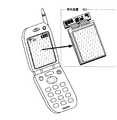
図9に示すように、携帯電話等の電子機器の表示部として発光装置が使用される場合は、発光装置901という形で内蔵される。ここで、発光装置901とは、パネルと、発光装置を駆動するための信号処理用LSI、メモリ等を実装した基板とを接続した形態を指す。
【0052】
発光装置901をブロック図として、図4(A)に示す。発光装置901は、パネル450、駆動回路460を有する。
【0053】
駆動回路460は信号生成部411、電源部412を有する。電源部412は、外部バッテリーより供給される電源より、ソース信号線駆動回路、ゲート信号線駆動回路、発光素子、信号生成部411等に、それぞれ所望の複数の電圧値の電源を生成し、供給する。信号生成部411には、電源、映像信号、同期信号が入力され、表示装置450にて処理が出来るように、各種信号の変換を行う他、ソース信号線駆動回路、ゲート信号線駆動回路を駆動するためのクロック信号等を生成する。また、駆動回路460とパネル450との間に、入力電源を切り替えるための選択部413を設けている。
【0054】
また、パネル450は基板上に、画素部401、ソース信号線駆動回路402、書込用ゲート信号線駆動回路403、消去用ゲート信号線駆動回路404、電流供給線405、対向電極コンタクト406、FPC407等によって構成される。基板中央部には、画素部401が配置され、その周辺部には、ソース信号線駆動回路402、書込用ゲート信号線駆動回路403、消去用ゲート信号線駆動回路404等が配置されている。ソース信号線駆動回路402、書込用ゲート信号線駆動回路403、消去用ゲート信号線駆動回路404を駆動するための信号、及び電源の供給はFPC407を通じて、駆動回路460より行われる。EL素子の対向電極は、画素部401全体面に形成されており、FPC407を通じて、電位が与えられる。この対向電極の電位は、逆方向バイアス印加のため、選択部413により切り替えることが出来る。
【0055】
図4(B)は、選択部413をパネル450上に一体形成した例である。
【0056】
また、パネル450、選択部413、信号生成部411および電源部412を基板上に一体形成しても良い。
【0057】
[実施例2]
デジタル映像信号を用いて映像の表示を行う場合の、ソース信号線駆動回路の概略図を図5に、ゲート信号線駆動回路の概略図を図6に示す。
【0058】
ソース信号線駆動回路は、D−フリップフロップ501を複数段用いてなるシフトレジスタ502、第1のラッチ回路503a、第2のラッチ回路503b、レベルシフタ504、バッファ505等を有する。外部より入力される信号は、クロック信号(S−CK)、反転クロック信号(S−CKb)、スタートパルス(S−SP)、デジタル映像信号(Digital Video Data)である。図5のような構成の場合、デジタル映像信号は、例えば「1ビット目の1行目→2行目→・・・→最終行、2ビット目の1行目→2行目→・・・→最終行、3ビット目の1行目、2行目・・・・・・」というように、直列に入力される。
【0059】
まず、クロック信号、クロック反転信号、およびスタートパルスのタイミングに従って、シフトレジスタ502より、順次サンプリングパルスが出力される。続いて、サンプリングパルスは、第1のラッチ回路503aに入力され、サンプリングパルスが入力されたタイミングで、各列のデジタル映像信号を取り込み、保持する。
【0060】
最終段の第1のラッチ回路503aにおいてデジタル映像信号の保持が完了すると、水平帰線期間中にラッチパルスが入力され、このタイミングで、第1のラッチ回路503aにおいて保持されているデジタル映像信号は、一斉に第2のラッチ回路503bへと転送される。その後、レベルシフタにおいてパルスの振幅変換を受け、続いて、バッファにおいて映像信号波形が整形された後、それぞれのソース信号線S1〜Sxへと出力される。
【0061】
一方、ゲート信号線駆動回路は、D−フリップフロップ601を複数段用いてなるシフトレジスタ602、レベルシフタ603、バッファ604等を有する。外部より入力される信号は、クロック信号(G−CK)、反転クロック信号(G−CKb)、スタートパルス(G−SP)である。
【0062】
まず、クロック信号、クロック反転信号、およびスタートパルスのタイミングに従って、シフトレジスタ602より、順次パルスが出力される。続いて、レベルシフタ603によってパルスの振幅変換を受け、続いて、バッファにおいてパルス波形が整形された後、ゲート信号線G1〜Gyを順次選択するパルスとして、それぞれのゲート信号線へと出力される。最終行Gyでの選択が終了すると、垂直帰線期間を経たあと、再びシフトレジスタ602よりパルスが出力され、順にゲート信号線の選択を行う。
【0063】
[実施例3]
実施形態1に挙げた画素構成をSES駆動し、逆方向バイアスを印加させる場合の実際の駆動タイミングについて、図1を用いて説明する。図1(A)、(B)はタイミングチャート、図1(C)は対向電極の電位、図1(D)は画素構成を示す。
【0064】
図1(A)に示すように、1フレーム期間を4つのサブフレーム期間SF1〜SF4に分割している。各サブフレームはアドレス(書き込み)期間Ta、サステイン(発光)期間Tsを有する。また、アドレス(書き込み)期間Taがサステイン(発光)期間Tsよりも長いサブフレーム(ここではSF3、SF4が該当する)はアドレス(書き込み)期間Ta、サステイン(発光)期間Tsの他に、消去期間Tr、非発光期間Te、逆方向バイアス期間Tbを設けている。
【0065】
アドレス(書き込み)期間Taとは画素にデジタル映像信号を書き込む期間であり、サステイン(発光)期間Tsとはアドレス(書き込み)期間Taにおいて、書き込まれたデジタル映像信号に基づいて、EL素子が発光または非発光の状態をとり、表示を行う期間である。どのサブフレームでEL素子が発光するかによって、1フレーム期間あたりの各画素の発光時間が決まり、この発光時間の差によって階調表示を行う。
【0066】
消去期間TrとはEL素子を強制的に非発光状態にする信号を画素に入力する期間であり、非発光期間Teとは消去期間Trに入力された信号に基づいてEL素子が非発光状態となる期間である。また、逆方向バイアス期間Tbとは、EL素子に逆方向バイアスを印加している期間である。
【0067】
動作としては、まずSF1のアドレス(書き込み)期間Ta1において、1行目から順に書込用ゲート信号線112にパルスが入力され、スイッチング用TFT115がONし、駆動用TFT117をON、OFFするためのデジタル映像信号が各画素に書き込まれる。デジタル映像信号が書き込まれた行においては直ちにサステイン(発光)期間Ts1へと移る。1行目〜最終行まで書き込み作業が完了するとアドレス(書き込み)期間Ta1は終了する。サステイン(発光)期間Ta1が終了した後、再び、1行目より順に書込用ゲート信号線112にパルスが入力され、SF2のアドレス(書き込み)期間Ta2が開始され、サステイン(発光)期間Ts2へと移る。
【0068】
続いて、SF3のアドレス(書き込み)期間Ta3が開始される。ここで、サステイン(発光)期間Ts3はアドレス(書き込み)期間Ta3よりも短いため、サステイン(発光)期間Ts3終了後すぐに次のアドレス(書き込み)期間Ta4に移ることが出来ない。そのため、各行のサステイン(発光)期間Ts3が終了すると、消去期間Tr3が開始される。消去期間Tr3では、消去用ゲート信号線113に1行目から順にパルスが入力されて消去用TFT116がONし、EL素子118の発光を強制的に停止し、以後、非発光期間Te3となる。
【0069】
このとき、通常のSES駆動では、非発光期間の長さは1行目のサステイン(発光)期間が終了してから最終行のアドレス(書き込み)期間が終了するまでの間となる。非発光期間Teでは、駆動用TFT117のゲート電極の電位は保持されるため、駆動用TFT117はOFFし続ける。
【0070】
非表示期間Te3が終了した後、逆方向バイアス期間Tb3へと移る。逆方向バイアス期間Tb3は対向電極の電位を図1(C)に示すように変化させるため、消去期間Tr3が終了した後に、非発光期間Te3を通常のSES駆動の時よりも延長し、前記非発光期間中に設ける必要がある。
【0071】
逆方向バイアス期間Tb3においては、対向電極の電位を、スイッチ120をVc1からVc2に切り替えることによって、画素電極の電位よりも高くし、EL素子118に逆方向バイアスを印加する。
【0072】
所望の逆方向バイアス期間Tb3が終了した時点で、対向電極の電位をVc2からVc1へ切り替える。それと同時に、次のアドレス(書き込み)期間Ta4が開始される。以後、SF3と同様の動作を繰り返し、SF4が終了すると、1フレームが終了し、次のフレームへと移る。
【0073】
また、図1(D)においては、駆動用TFT117のゲート電極と電流供給線114との間に、コンデンサを描いていないが、駆動用TFT117のゲート電極の電位をある時間保持するコンデンサを設けてもよい。また、駆動用TFT117のチャネル容量が充分であるなら、コンデンサを設ける必要はない。また、消去用ゲート信号線駆動回路の構成を変更し、非発光期間において、駆動用TFT117が確実にOFFするようなゲート・ソース間電圧としておけば良い。
【0074】
また、ここでは、アドレス(書き込み)期間Taがサステイン(発光)期間Tsよりも長いサブフレームのみに消去期間Tr、非発光期間Te、逆方向バイアス期間Tbを設けたが、アドレス(書き込み)期間Taがサステイン(発光)期間Tsよりも短い、あるいは同じ長さのサブフレームにおいても、各期間を設け、EL素子に逆方向バイアスを印加しても良い。
【0075】
また、図1(A)では、消去期間Trが最終行まで完全に終了してから、逆方向バイアス期間Tbが開始されたが、図1(B)に示すように、消去期間Teの最終行と逆方向バイアス印加期間Tb3の開始を重ね、duty比を稼ぐことも出来る。
【0076】
[実施例4]
実施形態2に挙げた画素構成をSES駆動し、逆方向バイアスを印加させる場合の書込用ゲート信号線駆動回路を図8(A)、画素構成を図8(B)、を用いて説明する。
【0077】
図8(A)のゲート信号線駆動回路は、D−フリップフロップ801を複数段用いてなるシフトレジスタ802、レベルシフタ803、バッファ804、そして、選択回路805等を有する。外部より入力される信号は、クロック信号(G−CK)、反転クロック信号(G−CKb)、スタートパルス(G−SP)、そして、セレクト信号(G−SEL)である。図8(A)におけるスイッチ821が図8(B)の選択回路805に相当する。
【0078】
まず順方向バイアス期間において、クロック信号、クロック反転信号、およびスタートパルスのタイミングに従って、シフトレジスタ802より、順次パルスが出力される。続いて、レベルシフタ803によってパルスの振幅変換を受け、続いて、バッファにおいてパルス波形が整形された後、選択回路805に入力される。選択回路805において、セレクト信号によって選択されたバッファ804からの出力パルスが書込用ゲート信号線G1〜Gyへと順次出力される。最終行Gyでの選択が終了すると、垂直帰線期間を経たあと、再びシフトレジスタ802よりパルスが出力され、順にゲート信号線の選択を行う。
【0079】
また、逆方向バイアス期間においては、セレクト信号が切り換わり、バッファ出力に関わらず、スイッチング用TFT815がONになる電位が書込用ゲート信号線G1〜Gyへ一斉に出力される。この時、同時に全列のソース信号線811にはLレベルの電位が入力されている。よって、全画素のスイッチング用TFT815が一斉にONし、駆動用TFT817のゲート電極にLレベルの電位が入力され、駆動用TFT817がONする。駆動用TFT817がONすることによって、画素電極に電流供給線814の電位が入力される。
【0080】
逆方向バイアス期間には、対向電極819の電位がスイッチ820によってVc1からVc2に切り替えられるため、画素電極の電位よりも、対向電極819の電位が高くなり、EL素子に逆方向バイアスが印加される。
【0081】
[実施例5]
図7(A)に、実施形態1、2にて示した図1(D)、図8(B)の構成を有する画素を実際に作製した場合の素子のレイアウト例を示す。また、図7(A)において、X−X‘で示される部分の断面図を図7(B)に示す。
【0082】
図7(A)において、700は絶縁表面を有する基板である。基板700上には、駆動用TFT707等が設けられ、駆動用TFT707のソース・ドレイン領域を形成する不純物領域に接続されるように、配線材料でなるソース・ドレイン電極が形成され、そのうちの一方と、画素電極708が、重なり合う部分で接続するように設けられている。画素電極708上には、有機導電体膜712が設けられ、さらに有機薄膜(発光層)713が設けられている。有機薄膜(発光層)713上には、対向電極714が設けられている。対向電極714は、全ての画素で共通に接続されるように、ベタ付けの形で形成される。
【0083】
うち、本文中でEL素子と表記しているものは、図7(B)において、画素電極708、有機導電体膜712、有機薄膜(発光層)713、対向電極714の積層体に相当し、画素電極708と対向電極714のうちいずれか一方が陽極、他方が陰極となる。
【0084】
有機薄膜(発光層)713から発せられた光は、画素電極708もしくは対向電極714のうちいずれかを透過して発せられる。このとき、図7(B)において、画素電極側、すなわちTFT等が形成されている側に光が発せられる場合を下面出射、対向電極側に光が発せられる場合を上面出射と呼ぶ。
【0085】
下面出射の場合、画素電極708を透明導電膜によって形成される。逆に、上面出射の場合、対向電極714を透明導電膜によって形成される。
【0086】
なお、本実施例にて示した構成はあくまで一例であり、画素レイアウト、断面構成、EL素子の電極の積層順等に関してはこの限りではない。
【0087】
また、カラー表示の発光装置においては、R・G・Bそれぞれの発光色を持つEL素子を塗り分けても良いし、単色のEL素子をベタ付けの形で塗り、カラーフィルタによってR・G・Bの発光を得るようにしても良い。
【0088】
[実施例6]
本実施例においては、発光層として高分子化合物を適用し、さらに陽極と発光層との間に導電性高分子化合物からなるバッファ層を設けた発光素子において、直流駆動(常に順方向バイアスを印加)と交流駆動(順方向バイアスと逆方向バイアスを一定周期で交互に印加)を行った際の輝度劣化について測定を行った結果について述べる。
【0089】
図3(A)(B)は、順方向バイアス:3.7V、逆方向バイアス:1.7V、デューティ50%、交流周波数60Hzにおいて交流駆動を行った際の信頼性試験の結果を示している。図3(A)はリニアスケール、図3(B)はLOGスケールである。初期輝度は約400cd/cm2であった。比較用に、直流駆動(順方向バイアス:3.65V)を行った際の信頼性試験の結果も同時に示した。結果、直流駆動においては、400時間程度で輝度が半減したのに対し、交流駆動においては、約700時間経過後も、半減には至らなかった。
【0090】
図3(C)(D)は、順方向バイアス:3.8V、逆方向バイアス:1.7V、デューティ50%、交流周波数600Hzにおいて交流駆動を行った際の信頼性試験の結果を示している。図3(C)はリニアスケール、図3(D)はLOGスケールである。初期輝度は約300cd/cm2であった。比較用に、直流駆動(順方向バイアス:3.65V)を行ったさいの信頼性試験の結果も同時に示した。結果、直流駆動においては、500時間程度で輝度が半減したのに対し、交流駆動においては、約700時間経過後も、初期輝度の60%程度を保持していた。
【0091】
[実施例7]
発光素子を用いた発光装置は自発光型であるため、液晶ディスプレイに比べ、明るい場所での視認性に優れ、視野角が広い。従って、様々な電子機器の表示部に用いることが出来る。
【0092】
本発明の発光装置を用いた電子機器として、テレビ、ビデオカメラ、デジタルカメラ、ゴーグル型ディスプレイ(ヘッドマウントディスプレイ)、ナビゲーションシステム、音響再生装置(カーオーディオ、オーディオコンポ等)、ノート型パーソナルコンピュータ、ゲーム機器、携帯情報端末(モバイルコンピュータ、携帯電話、携帯型ゲーム機または電子書籍等)、記録媒体を備えた画像再生装置(具体的にはDigital Versatile Disc(DVD)等の記録媒体を再生し、その画像を表示しうるディスプレイを備えた装置)などが挙げられる。特に、斜め方向から画面を見る機会が多い携帯情報端末は、視野角の広さが重要視されるため、発光装置を用いることが望ましい。それら電子機器の具体例を図10に示す。
【0093】
図10(A)はELディスプレイであり、筐体1001、音声出力部1002、表示部1003等を含む。本発明の発光装置は表示部1003に用いることが出来る。発光装置は自発光型であるためバックライトが必要なく、液晶ディスプレイよりも薄い表示部とすることが出来る。なお、発光素子表示装置は、パソコン用、TV放送受信用、広告表示用などの全ての情報表示用表示装置が含まれる。
【0094】
また、図10(C)は大型のELディスプレイであり、図10(A)と同様に、筐体1021、音声出力部1022、表示部1023を含む。本発明の発光装置は表示部1023に用いることが出来る。
【0095】
図10(B)はモバイルコンピュータであり、本体1011、スタイラス1012、表示部1013、操作ボタン1014、外部インターフェイス1015等を含む。本発明の発光装置は表示部1013に用いることが出来る。
【0096】
図10(D)はゲーム機であり、本体1031、表示部1032、操作ボタン1033等を含む。本発明の発光装置は表示部1032に用いることが出来る。
【0097】
図10(E)は携帯電話であり、本体1041、音声出力部1042、音声入力部1043、表示部1044、操作スイッチ1045、アンテナ1046等を含む。本発明の発光装置は表示部1044に用いることが出来る。なお、表示部1044は黒色の背景に白色の文字を表示することで携帯電話の消費電流を抑えることが出来る。
【0098】
なお、将来的に有機発光材料の発光輝度が高くなれば、出力した画像情報を含む光をレンズ等で拡大投影してフロント型若しくはリア型のプロジェクターに用いることも可能となる。
【0099】
また、上記電子機器はインターネットやCATV(ケーブルテレビ)などの電子通信回線を通じて配信された情報を表示することが多くなり、特に動画情報を表示する機会が増してきている。有機発光材料の応答速度は非常に高いため、発光装置は動画表示に好ましい。
【0100】
また、色鮮やかなため臨場感あふれる大画面テレビにも適している。
【0101】
また、発光装置は発光している部分が電力を消費するため、発光部分が極力少なくなるように情報を表示することが望ましい。従って、携帯情報端末、特に携帯電話や音響再生装置のような文字情報を主とする表示部に発光装置を用いる場合には、非発光部分を背景として文字情報を発光部分で形成するように駆動することが望ましい。
【0102】
以上の様に、本発明の適用範囲は極めて広く、あらゆる分野の電子機器に用いることが可能である。また、本実施例の電子機器は実施例1〜5に示したいずれの構成の発光装置を用いても良い。
【0103】
【発明の効果】
本発明の発光装置によって、SES駆動において、定電流で駆動しているEL素子に、逆方向バイアスを印加し、信頼性を向上させることが可能となる。また、逆方向バイアスの印加は、対向電極のみを変化させることで行い、電流供給線を大きく変化させる際に問題となるゲート信号線駆動回路の電圧上昇によるTFTの耐圧、消費電力の増大を抑えることが出来る。さらに、逆方向バイアスを順方向バイアスより小さくすることで、信頼性向上を確保しつつ、消費電力の低減も行える。また、逆方向バイアス時の電位をソース信号線駆動回路あるいはゲート信号線駆動回路の電源電位と共通化することで、電源数の増加も抑えることが出来る。
【図面の簡単な説明】
【図1】 本発明の一実施形態を説明する図。
【図2】 3トランジスタを用いて構成される発光装置の画素構成を示す図。
【図3】 EL素子の信頼性試験結果を示す図。
【図4】 発光装置の構成を示すブロック図。
【図5】 ソース信号線駆動回路の構成例を示す図。
【図6】 ゲート信号線駆動回路の構成例を示す図。
【図7】 画素部の素子レイアウト例と断面図。
【図8】 ゲート信号線駆動回路の構成例を示す図。
【図9】 電子機器に内臓された発光装置の例を示す図。
【図10】 本発明が適用可能な電子機器の例を示す図。
【符号の説明】
111 ソース信号線
112 書き込み用ゲート信号線
113 消去用ゲート信号線
114 電流供給線
115 スイッチング用TFT
116 消去用TFT
117 駆動用TFT
118 EL素子
119 対向電極
120 スイッチ[0001]
BACKGROUND OF THE INVENTION
The present invention relates to a light emitting element and a driving method of a light emitting device formed by forming a thin film transistor (hereinafter referred to as TFT) on a substrate. Further, the present invention relates to an electronic device using the light emitting device for a display portion.
[0002]
Note that in this specification, an electroluminescence (EL) element is taken as an example of a typical light emitting element, and the EL element uses light emission (fluorescence) from singlet excitons. Both of those utilizing light emission (phosphorescence) from triplet excitons shall be shown.
[0003]
[Prior art]
In recent years, light-emitting devices having EL elements as self-luminous elements have been actively developed. Unlike the liquid crystal display device, the light emitting device is a self-luminous type. An EL element has a structure in which an EL layer is sandwiched between a pair of electrodes (anode and cathode), and the EL layer usually has a laminated structure. Typically, a laminated structure of “hole transport layer / light emitting layer / electron transport layer” can be given. This structure has very high luminous efficiency, and most EL display devices currently under research and development employ this structure.
[0004]
In addition, a structure in which a hole injection layer / a hole transport layer / a light emitting layer / an electron transport layer are stacked in this order on the anode, or a hole injection layer / a hole transport layer / a light emitting layer / an electron transport layer / an electron injection. A structure in which layers are stacked may be employed. You may dope a fluorescent pigment | dye etc. with respect to a light emitting layer.
[0005]
In this specification, all layers provided between a cathode and an anode are collectively referred to as an EL layer. Therefore, the above-described hole injection layer, hole transport layer, light emitting layer, electron transport layer, electron injection layer, and the like are all included in the EL layer.
[0006]
Then, a predetermined voltage is applied to the EL layer having the above structure between a pair of electrodes (both electrodes), whereby recombination of carriers occurs in the light emitting layer to emit light. At this time, the light emission luminance of the EL element is proportional to the current flowing through the EL element.
[0007]
There are two types of light-emitting devices: passive matrix type and active matrix type. The active matrix type is suitable for those that require high-speed operation because of the increase in the number of pixels and the display of moving images as resolution increases. ing.
[0008]
[Problems to be solved by the invention]
As a driving method of the EL element, there are a constant voltage driving for applying a constant voltage to the EL element and a constant current driving for supplying a constant current to the EL element. In the constant voltage drive, the electric resistance of the EL element changes due to temperature change, and the amount of current flowing to the EL element also changes. Further, the electrical resistance of the EL element increases due to the change with time, and the amount of current flowing to the EL element decreases. Since the luminance of the EL element is proportional to the current, the luminance also changes as the current changes. Therefore, constant current driving is desirable as a driving method of the EL element.
[0009]
However, apart from the change in the electric resistance of the EL element, there is a deterioration that the luminance of the EL element decreases with time even if a constant current is passed. In particular, the decrease in luminance due to deterioration of the EL element during initial lighting, which is called “initial deterioration”, is remarkable.
[0010]
Therefore, there is a method of applying a reverse bias to the EL element in order to suppress deterioration of the EL element and improve reliability.
[0011]
Japanese Patent Laid-Open No. 8-180972 discloses that as the reverse bias applied voltage, it is desirable that the reverse bias voltage is greater than or equal to the forward bias voltage.
[0012]
As a driving method of the active matrix light emitting device, there is a digital time gray scale method which is not easily affected by variation in characteristics of driving TFTs. This is because each pixel is composed of two transistors, a driving TFT and a switching TFT. One frame period is divided into an address (writing) period and a sustain (light emission) period, and the sum of the length of light emission time. This is to control the gradation.
[0013]
In addition, there is a digital time gray scale method that can realize high-precision multi-gradation display by using three transistors, a driving TFT, a switching TFT, and an erasing TFT for each pixel. In this specification, a digital time gray scale method using these three transistors for each pixel is defined as SES (Simultaneous Erase Scan) drive. The details of this SES drive are disclosed in Japanese Patent Laid-Open No. 2001-343933.
[0014]
Consider applying a reverse bias by SES driving and driving the EL with a constant current. In an active matrix light emitting device, in order to drive an EL element with a constant current, a high voltage is required because the driving TFT and the EL element are connected in series and the driving TFT is operated in a saturation region.
[0015]
Furthermore, when the reverse bias voltage is made larger than the forward bias voltage, a large change in the electrode having a large capacitive load causes a problem of an increase in power consumption. Also, depending on the reverse bias application method, the following problems may occur. A pixel configuration in the case of performing the SES driving method is shown in FIG. The reason will be described with reference to FIG.
[0016]
Each pixel has a
[0017]
Here, the switching
[0018]
First, a pulse (8 V) for turning on the switching
[0019]
Subsequently, when the driving
[0020]
Subsequently, a pulse (8V) for turning on the erasing TFT is input to the erasing
[0021]
Here, a case where a reverse bias period is provided in the non-light emitting period and a reverse bias is applied to the
[0022]
For example, when the potential of the
[0023]
However, paying attention to the switching
[0024]
In addition, when the reverse bias voltage is changed greatly, the voltage change is applied to the other portion that is capacitively coupled to the voltage changing portion (the
[0025]
Further, by making the reverse bias voltage (10V) larger than the forward bias voltage (8V), the change (27V) in the potential of the
[0026]
Therefore, the present invention aims at improving the reliability of an EL element while suppressing an increase in power consumption, and an AC driving method for applying a reverse bias to an EL element driven with a constant current in SES driving. Propose.
[0027]
[Means for Solving the Problems]
Japanese Patent Application No. 2002-025065 describes an example of a method for driving EL at a constant current in SES driving. In this SES drive, a reverse bias application period is provided in the non-light emission period.
[0028]
A reverse bias application method is characterized in that an electrode (opposite electrode) opposite to an electrode directly connected to a drain electrode or a source electrode of a driving TFT is changed with an EL element interposed therebetween.
[0029]
Further, the reverse bias voltage is made smaller than the forward bias voltage to reduce power consumption. Even at this time, the effect of improving the reliability by the reverse bias can be obtained.
[0030]
Further, by sharing the power supply when the counter electrode is reversely biased with the driver power supply in the panel, an increase in the number of power supplies in the panel can be prevented. Here, the forward bias voltage gradually increases from the light emission start voltage in order to drive the EL element at a constant current.
[0031]
The configuration of the present invention is shown below.
[0032]
The driving method of the light emitting device of the present invention is as follows:
A driving method of a light emitting device having a plurality of pixels provided with a light emitting element, and expressing gradation by controlling a difference in light emission time of the light emitting element,
A first step of writing a video signal to the pixel;
A second step of causing the light emitting element to emit light or not to emit light based on the written video signal;
After the second step, a third step forcing the light emitting element into a non-light emitting state;
A forward bias voltage V applied between the first electrode and the second electrode of the light emitting element between the first electrode and the second electrode of the light emitting element when the light emitting element emits light.1 Reverse bias voltage V with the polarity reversed2 A fourth step of applying
And | V1 | ≧ | V2 It is characterized by that.
[0033]
The driving method of the light emitting device of the present invention is as follows:
A driving method of a light emitting device having a plurality of pixels provided with a light emitting element, and expressing gradation by controlling a difference in light emission time of the light emitting element,
One frame period has n (n is a natural number, 2 <n) subframe periods,
Each of the sub-frame periods includes an address period in which a video signal is written to a pixel and a sustain period in which display is performed by controlling light emission or non-light emission of the light emitting element based on the video signal written to the pixel. Have
In each of m (m is a natural number, 0 <m ≦ n−1) subframe periods selected from the n subframe periods, a reset signal is written to the pixel after the end of the sustain period. M reset periods whose periods do not overlap each other and m erasing periods whose periods do not overlap each other forcibly set the light emitting element in a non-light emitting state in the row in which the reset signal is written. ,
The k subframe periods (k is a natural number, 0 <k ≦ m) selected from the m subframe periods are respectively connected to the first electrode and the second electrode of the light emitting element when the light emitting element emits light. Forward bias voltage V applied between the electrodes1 Reverse bias voltage V with the polarity reversed2 And k reverse bias application periods whose periods do not overlap each other,
The address period, the sustain period, the reset period, the erase period, the reverse bias period, and the reverse bias application period each have a period that partially overlaps each other,
And | V1 | ≧ | V2 It is characterized by that.
[0034]
In the driving method of the light emitting device of the present invention described above,
The light emitting element to which the forward bias voltage is applied is driven with a constant current during a period in which the light emitting element emits light or does not emit light to display a screen.
[0035]
In the driving method of the light emitting device of the present invention described above,
The change from the forward bias voltage to the reverse bias voltage is performed by changing only the counter electrode of the light emitting element.
[0036]
DETAILED DESCRIPTION OF THE INVENTION
[Embodiment 1]
A pixel structure for solving the problem and driving thereof will be described with reference to FIG.
[0037]
Each pixel includes a
[0038]
Here, the switching
[0039]
During the period in which the forward bias is applied to the
[0040]
Subsequently, when the driving TFT 117 is turned on, a current flows from the current supply line 114 (5 V) to the counter electrode 119 (−10 V) having a potential of Vc1, and light is emitted. At this time, the driving TFT 117 operates in a saturation region. When the driving TFT 117 is OFF, no current flows through the
[0041]
Subsequently, a pulse is input to the erasing
[0042]
When the reverse bias period is applied to the
[0043]
Through the above operation, a reverse bias voltage is applied to the EL element. This makes it possible to suppress the initial deterioration of the EL element, which has been considered a problem. Further, since only the counter electrode is changed when applying the reverse bias voltage, the driving TFT and the erasing TFT connected to the current supply line have no influence on the gate-source voltage. Therefore, the power consumption of the gate signal line driving circuit is not greatly increased.
[0044]
[Embodiment 2]
A pixel configuration for solving the problem and driving thereof will be described with reference to FIG.
[0045]
Each of the write gate signal lines has a
[0046]
The operation at the time of forward bias is the same as that of the first embodiment. At the time of reverse bias, the potential of the counter electrode is switched to Vc2 (8V). The power source of Vc2 is preferably shared with the power source of the source signal line driver circuit or the gate signal line driver circuit. Here, it is made common with the power source of the source signal line driver circuit.
[0047]
Next, the source signal line driver circuit is operated so that the potentials of the source signal lines all become L level (0 V).
[0048]
Further, the potentials of the write gate signal lines in all rows are set to Vc4 (10 V) by using the
[0049]
According to this embodiment, as compared with the first embodiment, the potential of the pixel electrode when the reverse bias is applied is lowered by the threshold voltage of the driving TFT. As a result, when the same reverse bias voltage is applied, the potential of the counter electrode during the reverse bias can be lowered by the threshold voltage of the driving TFT, and power consumption can be reduced.
[0050]
【Example】
Examples of the present invention will be described below.
[0051]
[Example 1]
As shown in FIG. 9, when a light emitting device is used as a display unit of an electronic device such as a mobile phone, the
[0052]
FIG. 4A illustrates the light-emitting
[0053]
The drive circuit 460 includes a signal generation unit 411 and a power supply unit 412. The power supply unit 412 generates and supplies power of a plurality of desired voltage values to the source signal line drive circuit, the gate signal line drive circuit, the light emitting element, the signal generation unit 411, and the like from the power supplied from the external battery. To do. The signal generator 411 receives a power source, a video signal, and a synchronization signal, converts various signals so that the display device 450 can process them, and drives a source signal line driver circuit and a gate signal line driver circuit. For generating a clock signal or the like. A selection unit 413 for switching input power is provided between the drive circuit 460 and the panel 450.
[0054]
The panel 450 includes a pixel portion 401, a source signal line driving circuit 402, a writing gate signal line driving circuit 403, an erasing gate signal line driving circuit 404, a current supply line 405, a counter electrode contact 406, and an
[0055]
FIG. 4B shows an example in which the selection unit 413 is integrally formed on the panel 450.
[0056]
Further, the panel 450, the selection unit 413, the signal generation unit 411, and the power supply unit 412 may be integrally formed on the substrate.
[0057]
[Example 2]
FIG. 5 shows a schematic diagram of a source signal line driver circuit and FIG. 6 shows a schematic diagram of a gate signal line driver circuit when displaying an image using a digital video signal.
[0058]
The source signal line driver circuit includes a
[0059]
First, sampling pulses are sequentially output from the
[0060]
When the holding of the digital video signal is completed in the
[0061]
On the other hand, the gate signal line driver circuit includes a
[0062]
First, pulses are sequentially output from the
[0063]
[Example 3]
The actual drive timing when the pixel configuration described in
[0064]
As shown in FIG. 1A, one frame period is divided into four subframe periods SF1 to SF4. Each sub-frame has an address (writing) period Ta and a sustain (light emission) period Ts. In addition, the address (write) period Ta is longer than the sustain (light emission) period Ts, and the subframe (here, SF3 and SF4 correspond) is an erase period in addition to the address (write) period Ta and the sustain (light emission) period Ts. Tr, a non-light emitting period Te, and a reverse bias period Tb are provided.
[0065]
The address (writing) period Ta is a period during which a digital video signal is written to the pixel, and the sustain (light emission) period Ts is a period during which the EL element emits light based on the written digital video signal during the address (writing) period Ta. This is a period during which display is performed in a non-light emitting state. The light emission time of each pixel per frame period is determined depending on which subframe the EL element emits light, and gradation display is performed by the difference in the light emission time.
[0066]
The erasing period Tr is a period in which a signal for forcibly setting the EL element to a non-light emitting state is input to the pixel. It is a period. The reverse bias period Tb is a period during which a reverse bias is applied to the EL element.
[0067]
As an operation, first, in the address (write) period Ta1 of SF1, a pulse is inputted to the write
[0068]
Subsequently, the address (write) period Ta3 of SF3 is started. Here, since the sustain (light emission) period Ts3 is shorter than the address (write) period Ta3, it is not possible to move to the next address (write) period Ta4 immediately after the end of the sustain (light emission) period Ts3. Therefore, when the sustain (light emission) period Ts3 of each row ends, the erase period Tr3 starts. In the erasing period Tr3, pulses are sequentially input to the erasing
[0069]
At this time, in normal SES driving, the length of the non-light emission period is from the end of the first row sustain (light emission) period to the end of the last row address (write) period. In the non-light emitting period Te, the potential of the gate electrode of the driving TFT 117 is held, so that the driving TFT 117 is kept off.
[0070]
After the non-display period Te3 ends, the process proceeds to the reverse bias period Tb3. In the reverse bias period Tb3, the potential of the counter electrode is changed as shown in FIG. 1C. Therefore, after the erasing period Tr3 ends, the non-light emitting period Te3 is extended as compared with the normal SES driving, and the non-emitting period It is necessary to provide it during the light emission period.
[0071]
In the reverse bias period Tb3, the potential of the counter electrode is changed from Vc1 to Vc2 by switching the
[0072]
At the end of the desired reverse bias period Tb3, the potential of the counter electrode is set to Vc.2 To
[0073]
In FIG. 1D, a capacitor is not drawn between the gate electrode of the driving TFT 117 and the
[0074]
Here, only the subframe in which the address (write) period Ta is longer than the sustain (light emission) period Ts is provided with the erasure period Tr, the non-light emission period Te, and the reverse bias period Tb, but the address (write) period Ta However, each period may be provided in a subframe shorter than or equal to the sustain (light emission) period Ts, and a reverse bias may be applied to the EL element.
[0075]
In FIG. 1A, the reverse bias period Tb is started after the erasing period Tr is completely completed until the last row. As shown in FIG. 1B, the last row of the erasing period Te is started. And the reverse bias application period Tb3 can be repeated to increase the duty ratio.
[0076]
[Example 4]
A gate signal line driver circuit for writing when the pixel configuration described in Embodiment 2 is driven by SES and a reverse bias is applied will be described with reference to FIG. 8A and the pixel configuration will be described with reference to FIG. .
[0077]
The gate signal line driver circuit in FIG. 8A includes a
[0078]
First, in the forward bias period, pulses are sequentially output from the
[0079]
In the reverse bias period, the select signal is switched, and the potential at which the switching
[0080]
In the reverse bias period, since the potential of the
[0081]
[Example 5]
FIG. 7A shows a layout example of an element when a pixel having the configuration of FIGS. 1D and 8B shown in
[0082]
In FIG. 7A,
[0083]
Among them, what is described as an EL element in the text corresponds to a stacked body of a
[0084]
Light emitted from the organic thin film (light emitting layer) 713 is emitted through either the
[0085]
In the case of bottom emission, the
[0086]
Note that the structure shown in this embodiment is merely an example, and the pixel layout, the cross-sectional structure, the stacking order of the electrodes of the EL element, and the like are not limited thereto.
[0087]
In a light emitting device for color display, EL elements having emission colors of R, G, and B may be separately applied, or a monochrome EL element is applied in a solid form, and R, G, and B are applied by a color filter. B light emission may be obtained.
[0088]
[Example 6]
In this example, in a light emitting device in which a polymer compound is applied as a light emitting layer and a buffer layer made of a conductive polymer compound is provided between the anode and the light emitting layer, direct current drive (always applying a forward bias) ) And AC drive (forward bias and reverse bias are alternately applied at a constant period) and the results of measurement of luminance degradation are described.
[0089]
FIGS. 3A and 3B show the results of a reliability test when AC driving is performed at a forward bias of 3.7 V, a reverse bias of 1.7 V, a duty of 50%, and an AC frequency of 60 Hz. . 3A is a linear scale, and FIG. 3B is a LOG scale. Initial brightness is about 400cd / cm2 Met. For comparison, the results of a reliability test when DC driving (forward bias: 3.65 V) was performed are also shown. As a result, in the direct current drive, the luminance was reduced by half in about 400 hours, whereas in the alternating current drive, even after about 700 hours, the brightness was not reduced to half.
[0090]
3C and 3D show the results of a reliability test when AC driving is performed at a forward bias of 3.8 V, a reverse bias of 1.7 V, a duty of 50%, and an AC frequency of 600 Hz. . 3C is a linear scale, and FIG. 3D is a LOG scale. Initial brightness is about 300cd / cm2 Met. For comparison, the results of a reliability test when DC driving (forward bias: 3.65 V) was performed are also shown. As a result, in the direct current drive, the luminance was reduced by half in about 500 hours, whereas in the alternating current drive, about 60% of the initial luminance was maintained even after about 700 hours had elapsed.
[0091]
[Example 7]
Since a light-emitting device using a light-emitting element is a self-luminous type, it has excellent visibility in a bright place and a wide viewing angle compared to a liquid crystal display. Therefore, it can be used for display portions of various electronic devices.
[0092]
As an electronic device using the light emitting device of the present invention, a television, a video camera, a digital camera, a goggle type display (head mounted display), a navigation system, an audio playback device (car audio, audio component, etc.), a notebook personal computer, a game A device, a portable information terminal (mobile computer, mobile phone, portable game machine, electronic book, etc.), an image playback device equipped with a recording medium (specifically, a recording medium such as a digital versatile disc (DVD)) And a device having a display capable of displaying an image). In particular, it is desirable to use a light-emitting device for a portable information terminal that often has an opportunity to see a screen from an oblique direction because the wide viewing angle is important. Specific examples of these electronic devices are shown in FIGS.
[0093]
FIG. 10A illustrates an EL display, which includes a
[0094]
FIG. 10C illustrates a large EL display, which includes a
[0095]
FIG. 10B illustrates a mobile computer, which includes a
[0096]
FIG. 10D illustrates a game machine, which includes a
[0097]
FIG. 10E illustrates a mobile phone, which includes a
[0098]
If the light emission luminance of the organic light emitting material is increased in the future, the light including the output image information can be enlarged and projected by a lens or the like and used in a front type or rear type projector.
[0099]
In addition, the electronic devices often display information distributed through electronic communication lines such as the Internet and CATV (cable television), and in particular, opportunities to display moving image information are increasing. Since the organic light emitting material has a very high response speed, the light emitting device is preferable for displaying moving images.
[0100]
It is also suitable for large-screen TVs that are vivid and vivid.
[0101]
In addition, since the light emitting device consumes power in the light emitting portion, it is desirable to display information so that the light emitting portion is minimized. Therefore, when a light emitting device is used for a display unit mainly including character information, such as a portable information terminal, particularly a mobile phone or a sound reproduction device, it is driven so that character information is formed by the light emitting part with the non-light emitting part as the background. It is desirable to do.
[0102]
As described above, the applicable range of the present invention is so wide that it can be used for electronic devices in various fields. In addition, the electronic device of this embodiment may use the light emitting device having any structure shown in
[0103]
【The invention's effect】
With the light emitting device of the present invention, in SES driving, it becomes possible to apply a reverse bias to an EL element driven with a constant current and improve reliability. Further, the reverse bias is applied by changing only the counter electrode, and the increase in the breakdown voltage and power consumption of the TFT due to the rise in the voltage of the gate signal line driving circuit, which becomes a problem when the current supply line is greatly changed, is suppressed. I can do it. Furthermore, by making the reverse bias smaller than the forward bias, it is possible to reduce power consumption while ensuring improved reliability. Further, by sharing the potential at the time of reverse bias with the power source potential of the source signal line driver circuit or the gate signal line driver circuit, an increase in the number of power sources can be suppressed.
[Brief description of the drawings]
FIG. 1 illustrates one embodiment of the present invention.
FIG. 2 is a diagram showing a pixel configuration of a light-emitting device configured using three transistors.
FIG. 3 is a view showing a reliability test result of an EL element.
FIG. 4 is a block diagram illustrating a structure of a light emitting device.
FIG. 5 is a diagram showing a configuration example of a source signal line driver circuit.
FIG. 6 is a diagram showing a configuration example of a gate signal line driver circuit.
FIGS. 7A and 7B are an element layout example and a cross-sectional view of a pixel portion. FIGS.
FIG. 8 is a diagram showing a configuration example of a gate signal line driver circuit.
FIG. 9 illustrates an example of a light-emitting device incorporated in an electronic device.
FIG. 10 is a diagram showing an example of an electronic apparatus to which the invention can be applied.
[Explanation of symbols]
111 Source signal line
112 Write gate signal line
113 Erasing gate signal line
114 Current supply line
115 TFT for switching
116 Erase TFT
117 Driving TFT
118 EL element
119 Counter electrode
120 switches
Claims (5)
Translated fromJapanese前記複数の画素は、それぞれ、ソース信号線、書込用ゲート信号線、消去用ゲート信号線、スイッチング用薄膜トランジスタ、消去用薄膜トランジスタ、駆動用薄膜トランジスタ、発光素子、及び電流供給線を有し、
前記スイッチング用薄膜トランジスタのゲートは前記書込用ゲート信号線と電気的に接続され、ソース又はドレインの一方は前記ソース信号線と電気的に接続され、前記ソース又はドレインの他方は前記消去用薄膜トランジスタのソース又はドレインの一方及び前記駆動用薄膜トランジスタのゲートと電気的に接続され、
前記消去用薄膜トランジスタのゲートは前記消去用ゲート信号線と電気的に接続され、前記ソース又はドレインの他方は前記電流供給線と電気的に接続され、
前記駆動用薄膜トランジスタのソース又はドレインの一方は前記発光素子の一方と電気的に接続され、前記ソース又はドレインの他方は前記電流供給線と電気的に接続され、
前記発光素子の他方は対向電極と電気的に接続され、
1フレーム期間は、n個(nは自然数、2<n)のサブフレーム期間を有し、
前記n個のサブフレーム期間より選ばれたm個(mは自然数、0<m≦n−1)のサブフレーム期間それぞれは、第1の期間、第2の期間、第3の期間、及び第4の期間を有し、
前記m個のサブフレーム期間において、前記行ごとに、前記第1の期間、前記第2の期間、前記第3の期間、前記第4の期間を順に有し、
前記第1の期間において、前記スイッチング用薄膜トランジスタがオン、前記消去用薄膜トランジスタがオフになり、
前記第2の期間において、前記スイッチング用薄膜トランジスタがオフ、前記駆動用薄膜トランジスタがオン又はオフ、前記消去用薄膜トランジスタがオフになり、
前記第3の期間において、前記スイッチング用薄膜トランジスタがオフ、前記消去用薄膜トランジスタがオンになり、
前記第4の期間において、前記発光素子は非発光状態であり、
前記第4の期間内に、前記対向電極の電位を変化させることによって前記発光素子に逆方向バイアス電圧を印加する逆方向バイアス電圧印加期間を有し、
前記逆方向バイアス電圧は前記複数の行に配置された複数の画素全ての前記発光素子に対して同時に印加され、前記逆方向バイアス電圧印加期間が前記複数の行全ての前記第4の期間と重複する
ことを特徴とする発光装置の駆動方法。A method of driving a light emitting device which have a plurality ofpixels arranged in a plurality of rows,
Each of theplurality of pixels includesa source signal line, a writing gate signal line, an erasing gate signal line, a switching thin film transistor, an erasing thin film transistor, a driving thin film transistor, a light emitting element,and a current supply line.
The gate of the switching thin film transistor is electrically connected to the write gate signal line, one of the source and drain is electrically connected to the source signal line, and the other of the source or drain is the erase thin film transistor. Electrically connected to one of a source or a drain and a gate of the driving thin film transistor;
The gate of the erasing thin film transistor is electrically connected to the erasing gate signal line, the other of the source or drain is electrically connected to the current supply line,
One of the source and drain of the driving thin film transistor is electrically connected to one of the light emitting elements, and the other of the source and drain is electrically connected to the current supply line,
The other of the light emitting elementsis electrically connected to the counter electrode;
One frame period has n (n is a natural number, 2 <n) subframe periods,
Each of the m (m is a natural number, 0 <m ≦ n−1) subframe periods selected from the n subframe periodsincludes afirst period, a second period, a third period,and a first period. Has a period of4
In the m subframe periods, each row includes the first period, the second period, the third period, and the fourth period in order.
In the first period, the switching thin film transistor is turned on, the erasing thin film transistor is turned off,
In the second period, the switching thin film transistor is turned off, the driving thin film transistor is turned on or off, the erasing thin film transistor is turned off,
In the third period, the switching thin film transistor is turned off, the erasing thin film transistor is turned on,
In the fourth period, the light emitting element is in a non-light emitting state,
In the fourth period, it has a reverse bias voltage application periodfor applying a reverse bias voltage to the thus the light-emitting elementby changing the potential of the counter electrode,
The reverse bias voltage is simultaneously applied to the light emitting elements of all of the plurality of pixels arranged in the plurality of rows, and the reverse biasvoltage application period overlaps withthe fourth period of all of the plurality of rows. A method for driving a light-emitting device.
前記第1の期間において、前記スイッチング用薄膜トランジスタのゲートに前記書込用ゲート信号線からパルスが入力され、前記スイッチング用薄膜トランジスタをオンにし、前記スイッチング用薄膜トランジスタを介して前記駆動用薄膜トランジスタのゲートに前記ソース信号線から映像信号を印加し、前記駆動用薄膜トランジスタをオン又はオフさせることによって前記画素への書き込みを行い、
前記第2の期間において、前記駆動用薄膜トランジスタがオン時には前記駆動用薄膜トランジスタを介して前記発光素子に前記電流供給線から電流を流して前記発光素子を発光状態にし、前記駆動用薄膜トランジスタがオフ時には前記駆動用薄膜トランジスタを介して前記発光素子に前記電流供給線から電流が流れず前記発光素子を非発光状態にし、
前記第3の期間において、前記消去用薄膜トランジスタのゲートに前記消去用ゲート信号線からパルスが入力され、前記消去用薄膜トランジスタをオンさせることによって前記画素にリセット信号の書き込みを行い、
前記第4の期間において、前記消去用薄膜トランジスタを介して前記駆動用薄膜トランジスタのゲートに前記電流供給線の電位を入力するとともに前記駆動用薄膜トランジスタのソース又はドレインの他方に前記電流供給線の電位を入力して、前記駆動用薄膜トランジスタをオフさせることによって前記発光素子を前記非発光状態とすることを特徴とする発光装置の駆動方法。In claim 1,
Inthe first period,the pulse from the writing gate signal line is input to the gate of the switching thin film transistor, and turning on the switching thin film transistor,the gate of the driving thin film transistor via the switching thin film transistor applyinga video signal from the source signal line, to write tothe pixels by turning on or off the driving thin film transistor,
Inthe second period, when the driving thin film transistor is turned on, acurrent is supplied from the currentsupply line to the light emitting element through the driving thin film transistor to bring the lightemitting element into a light emitting state, and when the driving thin film transistor is turned off, A current does not flowfrom the currentsupply line to the light emitting element via the driving thin film transistor, and thelight emitting element is brought into a non-light emitting state.
Inthe third period, thepulse is inputtedfrom the erasing gate signal line to the gate of the erasing TFT, writes reset signal tothe pixel by turning on the erase TFT,
Inthe fourth period, the potential of the current supply line is input tothe gate of the driving thin film transistor through the erasing thin film transistor, and the potential of the current supply line is input tothe other of the source anddrain of the driving thin film transistor to a method of driving a light emitting device which is characterized in that said light emitting element andthe non-emission stateby the turning off the driving thin film transistor.
前記スイッチング用薄膜トランジスタ、前記消去用薄膜トランジスタがNチャネル型薄膜トランジスタであり、
前記駆動用薄膜トランジスタがPチャネル型薄膜トランジスタであり、
前記発光素子において、前記駆動用薄膜トランジスタのソースまたはドレインと電気的に接続されている一方が陽極であり、前記対向電極と電気的に接続されている他方が陰極であることを特徴とする発光装置の駆動方法。In claim 1or claim 2 ,
The switching thin film transistor and the erasing thin film transistor are N-channel thin film transistors,
The driving thin film transistor is a P-channel thin film transistor;
In the light emitting element, a source or drain iselectrically connected toone and the anode of the driving thin film transistor, light emitting device whereinthe counterelectrode on the attachedother is characterized in that it is a cathode Driving method.
前記複数の行に配置された複数の画素全ての前記対向電極はスイッチと電気的に接続されており、The counter electrodes of all of the plurality of pixels arranged in the plurality of rows are electrically connected to a switch,
前記スイッチによって前記対向電極の電位を切り換えることにより前記発光素子に前記逆方向バイアス電圧又は順方向バイアス電圧を印加することを特徴とする発光装置の駆動方法。A driving method of a light emitting device, wherein the reverse bias voltage or the forward bias voltage is applied to the light emitting element by switching the potential of the counter electrode by the switch.
前記発光素子が発光するときに前記発光素子に印加される前記順方向バイアス電圧VThe forward bias voltage V applied to the light emitting element when the light emitting element emits light.11と前記順方向バイアス電圧に対して極性の反転した前記逆方向バイアス電圧VAnd the reverse bias voltage V with the polarity reversed with respect to the forward bias voltage.22は、Is
|V1|≧|V2|を満たすことを特徴とする発光装置の駆動方法。| V1 | ≧ | V2 | is satisfied, A driving method of a light emitting device.
Priority Applications (1)
| Application Number | Priority Date | Filing Date | Title |
|---|---|---|---|
| JP2003052746AJP4454943B2 (en) | 2002-03-01 | 2003-02-28 | Driving method of light emitting device |
Applications Claiming Priority (3)
| Application Number | Priority Date | Filing Date | Title |
|---|---|---|---|
| JP2002-55840 | 2002-03-01 | ||
| JP2002055840 | 2002-03-01 | ||
| JP2003052746AJP4454943B2 (en) | 2002-03-01 | 2003-02-28 | Driving method of light emitting device |
Publications (3)
| Publication Number | Publication Date |
|---|---|
| JP2003323159A JP2003323159A (en) | 2003-11-14 |
| JP2003323159A5 JP2003323159A5 (en) | 2006-03-30 |
| JP4454943B2true JP4454943B2 (en) | 2010-04-21 |
Family
ID=29552195
Family Applications (1)
| Application Number | Title | Priority Date | Filing Date |
|---|---|---|---|
| JP2003052746AExpired - Fee RelatedJP4454943B2 (en) | 2002-03-01 | 2003-02-28 | Driving method of light emitting device |
Country Status (1)
| Country | Link |
|---|---|
| JP (1) | JP4454943B2 (en) |
Families Citing this family (12)
| Publication number | Priority date | Publication date | Assignee | Title |
|---|---|---|---|---|
| US8421715B2 (en) | 2004-05-21 | 2013-04-16 | Semiconductor Energy Laboratory Co., Ltd. | Display device, driving method thereof and electronic appliance |
| US7482629B2 (en) | 2004-05-21 | 2009-01-27 | Semiconductor Energy Laboratory Co., Ltd. | Display device and electronic device |
| US7245297B2 (en) | 2004-05-22 | 2007-07-17 | Semiconductor Energy Laboratory Co., Ltd. | Display device and electronic device |
| US7332742B2 (en) | 2004-06-29 | 2008-02-19 | Semiconductor Energy Laboratory Co., Ltd. | Display device and electronic apparatus |
| CN100485762C (en) | 2004-07-30 | 2009-05-06 | 株式会社半导体能源研究所 | Display device, driving method of display device, and electronic apparatus |
| US8194006B2 (en) | 2004-08-23 | 2012-06-05 | Semiconductor Energy Laboratory Co., Ltd. | Display device, driving method of the same, and electronic device comprising monitoring elements |
| US7570233B2 (en) | 2004-11-24 | 2009-08-04 | Semiconductor Energy Laboratory Co., Ltd. | Display device |
| US7442950B2 (en) | 2004-12-06 | 2008-10-28 | Semiconductor Energy Laboratory Co., Ltd. | Light emitting device |
| US7812794B2 (en) | 2004-12-06 | 2010-10-12 | Semiconductor Energy Laboratory Co., Ltd. | Display device and driving method thereof |
| JP2012064570A (en) | 2010-08-20 | 2012-03-29 | Semiconductor Energy Lab Co Ltd | Illumination device |
| US9230994B2 (en) | 2010-09-15 | 2016-01-05 | Semiconductor Energy Laboratory Co., Ltd. | Liquid crystal display device |
| KR102251927B1 (en) | 2015-02-13 | 2021-05-17 | 삼성디스플레이 주식회사 | Pixel circuit and display device including the same |
- 2003
- 2003-02-28JPJP2003052746Apatent/JP4454943B2/ennot_activeExpired - Fee Related
Also Published As
| Publication number | Publication date |
|---|---|
| JP2003323159A (en) | 2003-11-14 |
Similar Documents
| Publication | Publication Date | Title |
|---|---|---|
| JP4024557B2 (en) | Light emitting device, electronic equipment | |
| US7023141B2 (en) | Light emitting device and drive method thereof | |
| US9324249B2 (en) | Electroluminescent display panel with reduced power consumption | |
| US20030214250A1 (en) | Light-emitting device, and electric device using the same | |
| JP4454943B2 (en) | Driving method of light emitting device | |
| JP2003255880A (en) | Semiconductor ic circuit and its driving method | |
| US7330162B2 (en) | Method of driving a light emitting device and electronic equipment | |
| JP2003280587A (en) | Display device, and display module and electronic apparatus using the same | |
| JP5116202B2 (en) | Driving method of display device | |
| JP4798874B2 (en) | EL display device and electric appliance using the same | |
| JP4198483B2 (en) | Display device, electronic equipment | |
| JP2003323157A (en) | Driving method of light emitting device and electronic equipment | |
| JP4421641B2 (en) | Driving method of light emitting device | |
| JP2004004638A (en) | Driving method for light emitting device | |
| JP2006178429A (en) | Light emitting system, and electronic equipment |
Legal Events
| Date | Code | Title | Description |
|---|---|---|---|
| A521 | Request for written amendment filed | Free format text:JAPANESE INTERMEDIATE CODE: A523 Effective date:20060213 | |
| A621 | Written request for application examination | Free format text:JAPANESE INTERMEDIATE CODE: A621 Effective date:20060213 | |
| A977 | Report on retrieval | Free format text:JAPANESE INTERMEDIATE CODE: A971007 Effective date:20091008 | |
| A131 | Notification of reasons for refusal | Free format text:JAPANESE INTERMEDIATE CODE: A131 Effective date:20091020 | |
| A521 | Request for written amendment filed | Free format text:JAPANESE INTERMEDIATE CODE: A523 Effective date:20091209 | |
| TRDD | Decision of grant or rejection written | ||
| A01 | Written decision to grant a patent or to grant a registration (utility model) | Free format text:JAPANESE INTERMEDIATE CODE: A01 Effective date:20100202 | |
| A01 | Written decision to grant a patent or to grant a registration (utility model) | Free format text:JAPANESE INTERMEDIATE CODE: A01 | |
| A61 | First payment of annual fees (during grant procedure) | Free format text:JAPANESE INTERMEDIATE CODE: A61 Effective date:20100203 | |
| FPAY | Renewal fee payment (event date is renewal date of database) | Free format text:PAYMENT UNTIL: 20130212 Year of fee payment:3 | |
| R150 | Certificate of patent or registration of utility model | Free format text:JAPANESE INTERMEDIATE CODE: R150 | |
| FPAY | Renewal fee payment (event date is renewal date of database) | Free format text:PAYMENT UNTIL: 20130212 Year of fee payment:3 | |
| FPAY | Renewal fee payment (event date is renewal date of database) | Free format text:PAYMENT UNTIL: 20130212 Year of fee payment:3 | |
| R250 | Receipt of annual fees | Free format text:JAPANESE INTERMEDIATE CODE: R250 | |
| R250 | Receipt of annual fees | Free format text:JAPANESE INTERMEDIATE CODE: R250 | |
| R250 | Receipt of annual fees | Free format text:JAPANESE INTERMEDIATE CODE: R250 | |
| R250 | Receipt of annual fees | Free format text:JAPANESE INTERMEDIATE CODE: R250 | |
| LAPS | Cancellation because of no payment of annual fees |