JP4454814B2 - Resin-sealed semiconductor device and manufacturing method thereof - Google Patents
Resin-sealed semiconductor device and manufacturing method thereofDownload PDFInfo
- Publication number
- JP4454814B2 JP4454814B2JP2000258423AJP2000258423AJP4454814B2JP 4454814 B2JP4454814 B2JP 4454814B2JP 2000258423 AJP2000258423 AJP 2000258423AJP 2000258423 AJP2000258423 AJP 2000258423AJP 4454814 B2JP4454814 B2JP 4454814B2
- Authority
- JP
- Japan
- Prior art keywords
- wiring pattern
- semiconductor device
- metal
- flat plate
- semiconductor chip
- Prior art date
- Legal status (The legal status is an assumption and is not a legal conclusion. Google has not performed a legal analysis and makes no representation as to the accuracy of the status listed.)
- Expired - Fee Related
Links
- 239000004065semiconductorSubstances0.000titleclaimsdescription107
- 238000004519manufacturing processMethods0.000titleclaimsdescription24
- 229910052751metalInorganic materials0.000claimsdescription81
- 239000002184metalSubstances0.000claimsdescription81
- 238000000034methodMethods0.000claimsdescription28
- 229920005989resinPolymers0.000claimsdescription19
- 239000011347resinSubstances0.000claimsdescription19
- 238000007789sealingMethods0.000claimsdescription15
- 239000010949copperSubstances0.000claimsdescription14
- 238000007747platingMethods0.000claimsdescription13
- 239000010931goldSubstances0.000claimsdescription11
- 229910052802copperInorganic materials0.000claimsdescription10
- 229910052737goldInorganic materials0.000claimsdescription7
- RYGMFSIKBFXOCR-UHFFFAOYSA-NCopperChemical group[Cu]RYGMFSIKBFXOCR-UHFFFAOYSA-N0.000claimsdescription4
- PCHJSUWPFVWCPO-UHFFFAOYSA-NgoldChemical compound[Au]PCHJSUWPFVWCPO-UHFFFAOYSA-N0.000claimsdescription2
- 239000010410layerSubstances0.000description61
- 239000000853adhesiveSubstances0.000description16
- 230000001070adhesive effectEffects0.000description16
- 239000000758substrateSubstances0.000description10
- 238000005530etchingMethods0.000description7
- 239000000463materialSubstances0.000description6
- 229920001721polyimidePolymers0.000description6
- 229910000679solderInorganic materials0.000description6
- 239000004642PolyimideSubstances0.000description5
- 238000005498polishingMethods0.000description5
- 239000004593EpoxySubstances0.000description4
- 239000011810insulating materialSubstances0.000description4
- KDLHZDBZIXYQEI-UHFFFAOYSA-NpalladiumSubstances[Pd]KDLHZDBZIXYQEI-UHFFFAOYSA-N0.000description4
- 229920001187thermosetting polymerPolymers0.000description4
- 229910052782aluminiumInorganic materials0.000description3
- 238000003486chemical etchingMethods0.000description3
- 238000005516engineering processMethods0.000description3
- 238000000206photolithographyMethods0.000description3
- 238000007650screen-printingMethods0.000description3
- 229910052709silverInorganic materials0.000description3
- 238000004544sputter depositionMethods0.000description3
- 239000004634thermosetting polymerSubstances0.000description3
- 229910045601alloyInorganic materials0.000description2
- 239000000956alloySubstances0.000description2
- 230000015572biosynthetic processEffects0.000description2
- 239000004020conductorSubstances0.000description2
- 230000000694effectsEffects0.000description2
- 239000003822epoxy resinSubstances0.000description2
- 238000000227grindingMethods0.000description2
- 239000007769metal materialSubstances0.000description2
- 229910052759nickelInorganic materials0.000description2
- 229910052763palladiumInorganic materials0.000description2
- 230000000149penetrating effectEffects0.000description2
- 230000002093peripheral effectEffects0.000description2
- 229920002120photoresistant polymerPolymers0.000description2
- 229920000647polyepoxidePolymers0.000description2
- 238000005549size reductionMethods0.000description2
- 238000004528spin coatingMethods0.000description2
- 238000009281ultraviolet germicidal irradiationMethods0.000description2
- JOYRKODLDBILNP-UHFFFAOYSA-NEthyl urethaneChemical compoundCCOC(N)=OJOYRKODLDBILNP-UHFFFAOYSA-N0.000description1
- 229910021578Iron(III) chlorideInorganic materials0.000description1
- ISWSIDIOOBJBQZ-UHFFFAOYSA-NPhenolChemical compoundOC1=CC=CC=C1ISWSIDIOOBJBQZ-UHFFFAOYSA-N0.000description1
- 239000012790adhesive layerSubstances0.000description1
- 239000000470constituentSubstances0.000description1
- 238000010276constructionMethods0.000description1
- 238000005553drillingMethods0.000description1
- 238000009713electroplatingMethods0.000description1
- 239000011521glassSubstances0.000description1
- 238000009413insulationMethods0.000description1
- RBTARNINKXHZNM-UHFFFAOYSA-Kiron trichlorideChemical compoundCl[Fe](Cl)ClRBTARNINKXHZNM-UHFFFAOYSA-K0.000description1
- 238000012986modificationMethods0.000description1
- 230000004048modificationEffects0.000description1
- PXHVJJICTQNCMI-UHFFFAOYSA-NnickelSubstances[Ni]PXHVJJICTQNCMI-UHFFFAOYSA-N0.000description1
- 238000000059patterningMethods0.000description1
- 239000009719polyimide resinSubstances0.000description1
- 238000003825pressingMethods0.000description1
- 238000007639printingMethods0.000description1
- 229920002050silicone resinPolymers0.000description1
- 239000010944silver (metal)Substances0.000description1
Images


Classifications
- H—ELECTRICITY
- H01—ELECTRIC ELEMENTS
- H01L—SEMICONDUCTOR DEVICES NOT COVERED BY CLASS H10
- H01L21/00—Processes or apparatus adapted for the manufacture or treatment of semiconductor or solid state devices or of parts thereof
- H01L21/02—Manufacture or treatment of semiconductor devices or of parts thereof
- H01L21/04—Manufacture or treatment of semiconductor devices or of parts thereof the devices having potential barriers, e.g. a PN junction, depletion layer or carrier concentration layer
- H01L21/50—Assembly of semiconductor devices using processes or apparatus not provided for in a single one of the groups H01L21/18 - H01L21/326 or H10D48/04 - H10D48/07 e.g. sealing of a cap to a base of a container
- H01L21/56—Encapsulations, e.g. encapsulation layers, coatings
- H01L21/568—Temporary substrate used as encapsulation process aid
- H—ELECTRICITY
- H01—ELECTRIC ELEMENTS
- H01L—SEMICONDUCTOR DEVICES NOT COVERED BY CLASS H10
- H01L23/00—Details of semiconductor or other solid state devices
- H01L23/28—Encapsulations, e.g. encapsulating layers, coatings, e.g. for protection
- H—ELECTRICITY
- H01—ELECTRIC ELEMENTS
- H01L—SEMICONDUCTOR DEVICES NOT COVERED BY CLASS H10
- H01L21/00—Processes or apparatus adapted for the manufacture or treatment of semiconductor or solid state devices or of parts thereof
- H01L21/02—Manufacture or treatment of semiconductor devices or of parts thereof
- H01L21/04—Manufacture or treatment of semiconductor devices or of parts thereof the devices having potential barriers, e.g. a PN junction, depletion layer or carrier concentration layer
- H01L21/48—Manufacture or treatment of parts, e.g. containers, prior to assembly of the devices, using processes not provided for in a single one of the groups H01L21/18 - H01L21/326 or H10D48/04 - H10D48/07
- H01L21/4814—Conductive parts
- H01L21/4846—Leads on or in insulating or insulated substrates, e.g. metallisation
- H01L21/4857—Multilayer substrates
- H—ELECTRICITY
- H01—ELECTRIC ELEMENTS
- H01L—SEMICONDUCTOR DEVICES NOT COVERED BY CLASS H10
- H01L21/00—Processes or apparatus adapted for the manufacture or treatment of semiconductor or solid state devices or of parts thereof
- H01L21/02—Manufacture or treatment of semiconductor devices or of parts thereof
- H01L21/04—Manufacture or treatment of semiconductor devices or of parts thereof the devices having potential barriers, e.g. a PN junction, depletion layer or carrier concentration layer
- H01L21/48—Manufacture or treatment of parts, e.g. containers, prior to assembly of the devices, using processes not provided for in a single one of the groups H01L21/18 - H01L21/326 or H10D48/04 - H10D48/07
- H01L21/4814—Conductive parts
- H01L21/4846—Leads on or in insulating or insulated substrates, e.g. metallisation
- H01L21/486—Via connections through the substrate with or without pins
- H—ELECTRICITY
- H01—ELECTRIC ELEMENTS
- H01L—SEMICONDUCTOR DEVICES NOT COVERED BY CLASS H10
- H01L23/00—Details of semiconductor or other solid state devices
- H01L23/28—Encapsulations, e.g. encapsulating layers, coatings, e.g. for protection
- H01L23/31—Encapsulations, e.g. encapsulating layers, coatings, e.g. for protection characterised by the arrangement or shape
- H01L23/3107—Encapsulations, e.g. encapsulating layers, coatings, e.g. for protection characterised by the arrangement or shape the device being completely enclosed
- H01L23/3121—Encapsulations, e.g. encapsulating layers, coatings, e.g. for protection characterised by the arrangement or shape the device being completely enclosed a substrate forming part of the encapsulation
- H01L23/3128—Encapsulations, e.g. encapsulating layers, coatings, e.g. for protection characterised by the arrangement or shape the device being completely enclosed a substrate forming part of the encapsulation the substrate having spherical bumps for external connection
- H—ELECTRICITY
- H01—ELECTRIC ELEMENTS
- H01L—SEMICONDUCTOR DEVICES NOT COVERED BY CLASS H10
- H01L24/00—Arrangements for connecting or disconnecting semiconductor or solid-state bodies; Methods or apparatus related thereto
- H01L24/01—Means for bonding being attached to, or being formed on, the surface to be connected, e.g. chip-to-package, die-attach, "first-level" interconnects; Manufacturing methods related thereto
- H01L24/42—Wire connectors; Manufacturing methods related thereto
- H01L24/47—Structure, shape, material or disposition of the wire connectors after the connecting process
- H01L24/49—Structure, shape, material or disposition of the wire connectors after the connecting process of a plurality of wire connectors
- H—ELECTRICITY
- H01—ELECTRIC ELEMENTS
- H01L—SEMICONDUCTOR DEVICES NOT COVERED BY CLASS H10
- H01L2221/00—Processes or apparatus adapted for the manufacture or treatment of semiconductor or solid state devices or of parts thereof covered by H01L21/00
- H01L2221/67—Apparatus for handling semiconductor or electric solid state devices during manufacture or treatment thereof; Apparatus for handling wafers during manufacture or treatment of semiconductor or electric solid state devices or components; Apparatus not specifically provided for elsewhere
- H01L2221/683—Apparatus for handling semiconductor or electric solid state devices during manufacture or treatment thereof; Apparatus for handling wafers during manufacture or treatment of semiconductor or electric solid state devices or components; Apparatus not specifically provided for elsewhere for supporting or gripping
- H01L2221/68304—Apparatus for handling semiconductor or electric solid state devices during manufacture or treatment thereof; Apparatus for handling wafers during manufacture or treatment of semiconductor or electric solid state devices or components; Apparatus not specifically provided for elsewhere for supporting or gripping using temporarily an auxiliary support
- H01L2221/68377—Apparatus for handling semiconductor or electric solid state devices during manufacture or treatment thereof; Apparatus for handling wafers during manufacture or treatment of semiconductor or electric solid state devices or components; Apparatus not specifically provided for elsewhere for supporting or gripping using temporarily an auxiliary support with parts of the auxiliary support remaining in the finished device
- H—ELECTRICITY
- H01—ELECTRIC ELEMENTS
- H01L—SEMICONDUCTOR DEVICES NOT COVERED BY CLASS H10
- H01L2224/00—Indexing scheme for arrangements for connecting or disconnecting semiconductor or solid-state bodies and methods related thereto as covered by H01L24/00
- H01L2224/01—Means for bonding being attached to, or being formed on, the surface to be connected, e.g. chip-to-package, die-attach, "first-level" interconnects; Manufacturing methods related thereto
- H01L2224/10—Bump connectors; Manufacturing methods related thereto
- H01L2224/15—Structure, shape, material or disposition of the bump connectors after the connecting process
- H01L2224/16—Structure, shape, material or disposition of the bump connectors after the connecting process of an individual bump connector
- H—ELECTRICITY
- H01—ELECTRIC ELEMENTS
- H01L—SEMICONDUCTOR DEVICES NOT COVERED BY CLASS H10
- H01L2224/00—Indexing scheme for arrangements for connecting or disconnecting semiconductor or solid-state bodies and methods related thereto as covered by H01L24/00
- H01L2224/01—Means for bonding being attached to, or being formed on, the surface to be connected, e.g. chip-to-package, die-attach, "first-level" interconnects; Manufacturing methods related thereto
- H01L2224/26—Layer connectors, e.g. plate connectors, solder or adhesive layers; Manufacturing methods related thereto
- H01L2224/31—Structure, shape, material or disposition of the layer connectors after the connecting process
- H01L2224/32—Structure, shape, material or disposition of the layer connectors after the connecting process of an individual layer connector
- H01L2224/321—Disposition
- H01L2224/32151—Disposition the layer connector connecting between a semiconductor or solid-state body and an item not being a semiconductor or solid-state body, e.g. chip-to-substrate, chip-to-passive
- H01L2224/32221—Disposition the layer connector connecting between a semiconductor or solid-state body and an item not being a semiconductor or solid-state body, e.g. chip-to-substrate, chip-to-passive the body and the item being stacked
- H01L2224/32225—Disposition the layer connector connecting between a semiconductor or solid-state body and an item not being a semiconductor or solid-state body, e.g. chip-to-substrate, chip-to-passive the body and the item being stacked the item being non-metallic, e.g. insulating substrate with or without metallisation
- H—ELECTRICITY
- H01—ELECTRIC ELEMENTS
- H01L—SEMICONDUCTOR DEVICES NOT COVERED BY CLASS H10
- H01L2224/00—Indexing scheme for arrangements for connecting or disconnecting semiconductor or solid-state bodies and methods related thereto as covered by H01L24/00
- H01L2224/01—Means for bonding being attached to, or being formed on, the surface to be connected, e.g. chip-to-package, die-attach, "first-level" interconnects; Manufacturing methods related thereto
- H01L2224/42—Wire connectors; Manufacturing methods related thereto
- H01L2224/44—Structure, shape, material or disposition of the wire connectors prior to the connecting process
- H01L2224/45—Structure, shape, material or disposition of the wire connectors prior to the connecting process of an individual wire connector
- H01L2224/45001—Core members of the connector
- H01L2224/45099—Material
- H01L2224/451—Material with a principal constituent of the material being a metal or a metalloid, e.g. boron (B), silicon (Si), germanium (Ge), arsenic (As), antimony (Sb), tellurium (Te) and polonium (Po), and alloys thereof
- H01L2224/45117—Material with a principal constituent of the material being a metal or a metalloid, e.g. boron (B), silicon (Si), germanium (Ge), arsenic (As), antimony (Sb), tellurium (Te) and polonium (Po), and alloys thereof the principal constituent melting at a temperature of greater than or equal to 400°C and less than 950°C
- H01L2224/45124—Aluminium (Al) as principal constituent
- H—ELECTRICITY
- H01—ELECTRIC ELEMENTS
- H01L—SEMICONDUCTOR DEVICES NOT COVERED BY CLASS H10
- H01L2224/00—Indexing scheme for arrangements for connecting or disconnecting semiconductor or solid-state bodies and methods related thereto as covered by H01L24/00
- H01L2224/01—Means for bonding being attached to, or being formed on, the surface to be connected, e.g. chip-to-package, die-attach, "first-level" interconnects; Manufacturing methods related thereto
- H01L2224/42—Wire connectors; Manufacturing methods related thereto
- H01L2224/44—Structure, shape, material or disposition of the wire connectors prior to the connecting process
- H01L2224/45—Structure, shape, material or disposition of the wire connectors prior to the connecting process of an individual wire connector
- H01L2224/45001—Core members of the connector
- H01L2224/45099—Material
- H01L2224/451—Material with a principal constituent of the material being a metal or a metalloid, e.g. boron (B), silicon (Si), germanium (Ge), arsenic (As), antimony (Sb), tellurium (Te) and polonium (Po), and alloys thereof
- H01L2224/45138—Material with a principal constituent of the material being a metal or a metalloid, e.g. boron (B), silicon (Si), germanium (Ge), arsenic (As), antimony (Sb), tellurium (Te) and polonium (Po), and alloys thereof the principal constituent melting at a temperature of greater than or equal to 950°C and less than 1550°C
- H01L2224/45144—Gold (Au) as principal constituent
- H—ELECTRICITY
- H01—ELECTRIC ELEMENTS
- H01L—SEMICONDUCTOR DEVICES NOT COVERED BY CLASS H10
- H01L2224/00—Indexing scheme for arrangements for connecting or disconnecting semiconductor or solid-state bodies and methods related thereto as covered by H01L24/00
- H01L2224/01—Means for bonding being attached to, or being formed on, the surface to be connected, e.g. chip-to-package, die-attach, "first-level" interconnects; Manufacturing methods related thereto
- H01L2224/42—Wire connectors; Manufacturing methods related thereto
- H01L2224/44—Structure, shape, material or disposition of the wire connectors prior to the connecting process
- H01L2224/45—Structure, shape, material or disposition of the wire connectors prior to the connecting process of an individual wire connector
- H01L2224/45001—Core members of the connector
- H01L2224/45099—Material
- H01L2224/451—Material with a principal constituent of the material being a metal or a metalloid, e.g. boron (B), silicon (Si), germanium (Ge), arsenic (As), antimony (Sb), tellurium (Te) and polonium (Po), and alloys thereof
- H01L2224/45138—Material with a principal constituent of the material being a metal or a metalloid, e.g. boron (B), silicon (Si), germanium (Ge), arsenic (As), antimony (Sb), tellurium (Te) and polonium (Po), and alloys thereof the principal constituent melting at a temperature of greater than or equal to 950°C and less than 1550°C
- H01L2224/45147—Copper (Cu) as principal constituent
- H—ELECTRICITY
- H01—ELECTRIC ELEMENTS
- H01L—SEMICONDUCTOR DEVICES NOT COVERED BY CLASS H10
- H01L2224/00—Indexing scheme for arrangements for connecting or disconnecting semiconductor or solid-state bodies and methods related thereto as covered by H01L24/00
- H01L2224/01—Means for bonding being attached to, or being formed on, the surface to be connected, e.g. chip-to-package, die-attach, "first-level" interconnects; Manufacturing methods related thereto
- H01L2224/42—Wire connectors; Manufacturing methods related thereto
- H01L2224/44—Structure, shape, material or disposition of the wire connectors prior to the connecting process
- H01L2224/45—Structure, shape, material or disposition of the wire connectors prior to the connecting process of an individual wire connector
- H01L2224/45001—Core members of the connector
- H01L2224/45099—Material
- H01L2224/451—Material with a principal constituent of the material being a metal or a metalloid, e.g. boron (B), silicon (Si), germanium (Ge), arsenic (As), antimony (Sb), tellurium (Te) and polonium (Po), and alloys thereof
- H01L2224/45163—Material with a principal constituent of the material being a metal or a metalloid, e.g. boron (B), silicon (Si), germanium (Ge), arsenic (As), antimony (Sb), tellurium (Te) and polonium (Po), and alloys thereof the principal constituent melting at a temperature of greater than 1550°C
- H01L2224/45164—Palladium (Pd) as principal constituent
- H—ELECTRICITY
- H01—ELECTRIC ELEMENTS
- H01L—SEMICONDUCTOR DEVICES NOT COVERED BY CLASS H10
- H01L2224/00—Indexing scheme for arrangements for connecting or disconnecting semiconductor or solid-state bodies and methods related thereto as covered by H01L24/00
- H01L2224/01—Means for bonding being attached to, or being formed on, the surface to be connected, e.g. chip-to-package, die-attach, "first-level" interconnects; Manufacturing methods related thereto
- H01L2224/42—Wire connectors; Manufacturing methods related thereto
- H01L2224/47—Structure, shape, material or disposition of the wire connectors after the connecting process
- H01L2224/48—Structure, shape, material or disposition of the wire connectors after the connecting process of an individual wire connector
- H01L2224/4805—Shape
- H01L2224/4809—Loop shape
- H01L2224/48091—Arched
- H—ELECTRICITY
- H01—ELECTRIC ELEMENTS
- H01L—SEMICONDUCTOR DEVICES NOT COVERED BY CLASS H10
- H01L2224/00—Indexing scheme for arrangements for connecting or disconnecting semiconductor or solid-state bodies and methods related thereto as covered by H01L24/00
- H01L2224/01—Means for bonding being attached to, or being formed on, the surface to be connected, e.g. chip-to-package, die-attach, "first-level" interconnects; Manufacturing methods related thereto
- H01L2224/42—Wire connectors; Manufacturing methods related thereto
- H01L2224/47—Structure, shape, material or disposition of the wire connectors after the connecting process
- H01L2224/48—Structure, shape, material or disposition of the wire connectors after the connecting process of an individual wire connector
- H01L2224/4805—Shape
- H01L2224/4809—Loop shape
- H01L2224/48095—Kinked
- H—ELECTRICITY
- H01—ELECTRIC ELEMENTS
- H01L—SEMICONDUCTOR DEVICES NOT COVERED BY CLASS H10
- H01L2224/00—Indexing scheme for arrangements for connecting or disconnecting semiconductor or solid-state bodies and methods related thereto as covered by H01L24/00
- H01L2224/01—Means for bonding being attached to, or being formed on, the surface to be connected, e.g. chip-to-package, die-attach, "first-level" interconnects; Manufacturing methods related thereto
- H01L2224/42—Wire connectors; Manufacturing methods related thereto
- H01L2224/47—Structure, shape, material or disposition of the wire connectors after the connecting process
- H01L2224/48—Structure, shape, material or disposition of the wire connectors after the connecting process of an individual wire connector
- H01L2224/481—Disposition
- H01L2224/48151—Connecting between a semiconductor or solid-state body and an item not being a semiconductor or solid-state body, e.g. chip-to-substrate, chip-to-passive
- H01L2224/48221—Connecting between a semiconductor or solid-state body and an item not being a semiconductor or solid-state body, e.g. chip-to-substrate, chip-to-passive the body and the item being stacked
- H01L2224/48225—Connecting between a semiconductor or solid-state body and an item not being a semiconductor or solid-state body, e.g. chip-to-substrate, chip-to-passive the body and the item being stacked the item being non-metallic, e.g. insulating substrate with or without metallisation
- H01L2224/48227—Connecting between a semiconductor or solid-state body and an item not being a semiconductor or solid-state body, e.g. chip-to-substrate, chip-to-passive the body and the item being stacked the item being non-metallic, e.g. insulating substrate with or without metallisation connecting the wire to a bond pad of the item
- H01L2224/48228—Connecting between a semiconductor or solid-state body and an item not being a semiconductor or solid-state body, e.g. chip-to-substrate, chip-to-passive the body and the item being stacked the item being non-metallic, e.g. insulating substrate with or without metallisation connecting the wire to a bond pad of the item the bond pad being disposed in a recess of the surface of the item
- H—ELECTRICITY
- H01—ELECTRIC ELEMENTS
- H01L—SEMICONDUCTOR DEVICES NOT COVERED BY CLASS H10
- H01L2224/00—Indexing scheme for arrangements for connecting or disconnecting semiconductor or solid-state bodies and methods related thereto as covered by H01L24/00
- H01L2224/01—Means for bonding being attached to, or being formed on, the surface to be connected, e.g. chip-to-package, die-attach, "first-level" interconnects; Manufacturing methods related thereto
- H01L2224/42—Wire connectors; Manufacturing methods related thereto
- H01L2224/47—Structure, shape, material or disposition of the wire connectors after the connecting process
- H01L2224/48—Structure, shape, material or disposition of the wire connectors after the connecting process of an individual wire connector
- H01L2224/484—Connecting portions
- H01L2224/48463—Connecting portions the connecting portion on the bonding area of the semiconductor or solid-state body being a ball bond
- H01L2224/48465—Connecting portions the connecting portion on the bonding area of the semiconductor or solid-state body being a ball bond the other connecting portion not on the bonding area being a wedge bond, i.e. ball-to-wedge, regular stitch
- H—ELECTRICITY
- H01—ELECTRIC ELEMENTS
- H01L—SEMICONDUCTOR DEVICES NOT COVERED BY CLASS H10
- H01L2224/00—Indexing scheme for arrangements for connecting or disconnecting semiconductor or solid-state bodies and methods related thereto as covered by H01L24/00
- H01L2224/01—Means for bonding being attached to, or being formed on, the surface to be connected, e.g. chip-to-package, die-attach, "first-level" interconnects; Manufacturing methods related thereto
- H01L2224/42—Wire connectors; Manufacturing methods related thereto
- H01L2224/47—Structure, shape, material or disposition of the wire connectors after the connecting process
- H01L2224/49—Structure, shape, material or disposition of the wire connectors after the connecting process of a plurality of wire connectors
- H01L2224/491—Disposition
- H01L2224/4911—Disposition the connectors being bonded to at least one common bonding area, e.g. daisy chain
- H—ELECTRICITY
- H01—ELECTRIC ELEMENTS
- H01L—SEMICONDUCTOR DEVICES NOT COVERED BY CLASS H10
- H01L2224/00—Indexing scheme for arrangements for connecting or disconnecting semiconductor or solid-state bodies and methods related thereto as covered by H01L24/00
- H01L2224/73—Means for bonding being of different types provided for in two or more of groups H01L2224/10, H01L2224/18, H01L2224/26, H01L2224/34, H01L2224/42, H01L2224/50, H01L2224/63, H01L2224/71
- H01L2224/732—Location after the connecting process
- H01L2224/73251—Location after the connecting process on different surfaces
- H01L2224/73265—Layer and wire connectors
- H—ELECTRICITY
- H01—ELECTRIC ELEMENTS
- H01L—SEMICONDUCTOR DEVICES NOT COVERED BY CLASS H10
- H01L24/00—Arrangements for connecting or disconnecting semiconductor or solid-state bodies; Methods or apparatus related thereto
- H01L24/01—Means for bonding being attached to, or being formed on, the surface to be connected, e.g. chip-to-package, die-attach, "first-level" interconnects; Manufacturing methods related thereto
- H01L24/42—Wire connectors; Manufacturing methods related thereto
- H01L24/44—Structure, shape, material or disposition of the wire connectors prior to the connecting process
- H01L24/45—Structure, shape, material or disposition of the wire connectors prior to the connecting process of an individual wire connector
- H—ELECTRICITY
- H01—ELECTRIC ELEMENTS
- H01L—SEMICONDUCTOR DEVICES NOT COVERED BY CLASS H10
- H01L24/00—Arrangements for connecting or disconnecting semiconductor or solid-state bodies; Methods or apparatus related thereto
- H01L24/01—Means for bonding being attached to, or being formed on, the surface to be connected, e.g. chip-to-package, die-attach, "first-level" interconnects; Manufacturing methods related thereto
- H01L24/42—Wire connectors; Manufacturing methods related thereto
- H01L24/47—Structure, shape, material or disposition of the wire connectors after the connecting process
- H01L24/48—Structure, shape, material or disposition of the wire connectors after the connecting process of an individual wire connector
- H—ELECTRICITY
- H01—ELECTRIC ELEMENTS
- H01L—SEMICONDUCTOR DEVICES NOT COVERED BY CLASS H10
- H01L2924/00—Indexing scheme for arrangements or methods for connecting or disconnecting semiconductor or solid-state bodies as covered by H01L24/00
- H01L2924/0001—Technical content checked by a classifier
- H01L2924/00014—Technical content checked by a classifier the subject-matter covered by the group, the symbol of which is combined with the symbol of this group, being disclosed without further technical details
- H—ELECTRICITY
- H01—ELECTRIC ELEMENTS
- H01L—SEMICONDUCTOR DEVICES NOT COVERED BY CLASS H10
- H01L2924/00—Indexing scheme for arrangements or methods for connecting or disconnecting semiconductor or solid-state bodies as covered by H01L24/00
- H01L2924/01—Chemical elements
- H01L2924/01005—Boron [B]
- H—ELECTRICITY
- H01—ELECTRIC ELEMENTS
- H01L—SEMICONDUCTOR DEVICES NOT COVERED BY CLASS H10
- H01L2924/00—Indexing scheme for arrangements or methods for connecting or disconnecting semiconductor or solid-state bodies as covered by H01L24/00
- H01L2924/01—Chemical elements
- H01L2924/01006—Carbon [C]
- H—ELECTRICITY
- H01—ELECTRIC ELEMENTS
- H01L—SEMICONDUCTOR DEVICES NOT COVERED BY CLASS H10
- H01L2924/00—Indexing scheme for arrangements or methods for connecting or disconnecting semiconductor or solid-state bodies as covered by H01L24/00
- H01L2924/01—Chemical elements
- H01L2924/01013—Aluminum [Al]
- H—ELECTRICITY
- H01—ELECTRIC ELEMENTS
- H01L—SEMICONDUCTOR DEVICES NOT COVERED BY CLASS H10
- H01L2924/00—Indexing scheme for arrangements or methods for connecting or disconnecting semiconductor or solid-state bodies as covered by H01L24/00
- H01L2924/01—Chemical elements
- H01L2924/01028—Nickel [Ni]
- H—ELECTRICITY
- H01—ELECTRIC ELEMENTS
- H01L—SEMICONDUCTOR DEVICES NOT COVERED BY CLASS H10
- H01L2924/00—Indexing scheme for arrangements or methods for connecting or disconnecting semiconductor or solid-state bodies as covered by H01L24/00
- H01L2924/01—Chemical elements
- H01L2924/01029—Copper [Cu]
- H—ELECTRICITY
- H01—ELECTRIC ELEMENTS
- H01L—SEMICONDUCTOR DEVICES NOT COVERED BY CLASS H10
- H01L2924/00—Indexing scheme for arrangements or methods for connecting or disconnecting semiconductor or solid-state bodies as covered by H01L24/00
- H01L2924/01—Chemical elements
- H01L2924/01047—Silver [Ag]
- H—ELECTRICITY
- H01—ELECTRIC ELEMENTS
- H01L—SEMICONDUCTOR DEVICES NOT COVERED BY CLASS H10
- H01L2924/00—Indexing scheme for arrangements or methods for connecting or disconnecting semiconductor or solid-state bodies as covered by H01L24/00
- H01L2924/01—Chemical elements
- H01L2924/01078—Platinum [Pt]
- H—ELECTRICITY
- H01—ELECTRIC ELEMENTS
- H01L—SEMICONDUCTOR DEVICES NOT COVERED BY CLASS H10
- H01L2924/00—Indexing scheme for arrangements or methods for connecting or disconnecting semiconductor or solid-state bodies as covered by H01L24/00
- H01L2924/01—Chemical elements
- H01L2924/01079—Gold [Au]
- H—ELECTRICITY
- H01—ELECTRIC ELEMENTS
- H01L—SEMICONDUCTOR DEVICES NOT COVERED BY CLASS H10
- H01L2924/00—Indexing scheme for arrangements or methods for connecting or disconnecting semiconductor or solid-state bodies as covered by H01L24/00
- H01L2924/013—Alloys
- H01L2924/014—Solder alloys
- H—ELECTRICITY
- H01—ELECTRIC ELEMENTS
- H01L—SEMICONDUCTOR DEVICES NOT COVERED BY CLASS H10
- H01L2924/00—Indexing scheme for arrangements or methods for connecting or disconnecting semiconductor or solid-state bodies as covered by H01L24/00
- H01L2924/06—Polymers
- H01L2924/078—Adhesive characteristics other than chemical
- H01L2924/07802—Adhesive characteristics other than chemical not being an ohmic electrical conductor
- H—ELECTRICITY
- H01—ELECTRIC ELEMENTS
- H01L—SEMICONDUCTOR DEVICES NOT COVERED BY CLASS H10
- H01L2924/00—Indexing scheme for arrangements or methods for connecting or disconnecting semiconductor or solid-state bodies as covered by H01L24/00
- H01L2924/15—Details of package parts other than the semiconductor or other solid state devices to be connected
- H01L2924/151—Die mounting substrate
- H01L2924/1517—Multilayer substrate
- H01L2924/15182—Fan-in arrangement of the internal vias
- H01L2924/15183—Fan-in arrangement of the internal vias in a single layer of the multilayer substrate
- H—ELECTRICITY
- H01—ELECTRIC ELEMENTS
- H01L—SEMICONDUCTOR DEVICES NOT COVERED BY CLASS H10
- H01L2924/00—Indexing scheme for arrangements or methods for connecting or disconnecting semiconductor or solid-state bodies as covered by H01L24/00
- H01L2924/15—Details of package parts other than the semiconductor or other solid state devices to be connected
- H01L2924/151—Die mounting substrate
- H01L2924/153—Connection portion
- H01L2924/1531—Connection portion the connection portion being formed only on the surface of the substrate opposite to the die mounting surface
- H01L2924/15311—Connection portion the connection portion being formed only on the surface of the substrate opposite to the die mounting surface being a ball array, e.g. BGA
- H—ELECTRICITY
- H01—ELECTRIC ELEMENTS
- H01L—SEMICONDUCTOR DEVICES NOT COVERED BY CLASS H10
- H01L2924/00—Indexing scheme for arrangements or methods for connecting or disconnecting semiconductor or solid-state bodies as covered by H01L24/00
- H01L2924/15—Details of package parts other than the semiconductor or other solid state devices to be connected
- H01L2924/181—Encapsulation
- H01L2924/1815—Shape
- H01L2924/1816—Exposing the passive side of the semiconductor or solid-state body
- H01L2924/18161—Exposing the passive side of the semiconductor or solid-state body of a flip chip
- H—ELECTRICITY
- H01—ELECTRIC ELEMENTS
- H01L—SEMICONDUCTOR DEVICES NOT COVERED BY CLASS H10
- H01L2924/00—Indexing scheme for arrangements or methods for connecting or disconnecting semiconductor or solid-state bodies as covered by H01L24/00
- H01L2924/19—Details of hybrid assemblies other than the semiconductor or other solid state devices to be connected
- H01L2924/191—Disposition
- H01L2924/19101—Disposition of discrete passive components
- H01L2924/19107—Disposition of discrete passive components off-chip wires
Landscapes
- Engineering & Computer Science (AREA)
- Microelectronics & Electronic Packaging (AREA)
- Computer Hardware Design (AREA)
- Power Engineering (AREA)
- Physics & Mathematics (AREA)
- Condensed Matter Physics & Semiconductors (AREA)
- General Physics & Mathematics (AREA)
- Manufacturing & Machinery (AREA)
- Ceramic Engineering (AREA)
- Wire Bonding (AREA)
- Encapsulation Of And Coatings For Semiconductor Or Solid State Devices (AREA)
- Internal Circuitry In Semiconductor Integrated Circuit Devices (AREA)
Description
Translated fromJapanese【0001】
【発明の属する技術分野】
本発明は、半導体装置及びその製造方法に関し、更に詳しくは、半導体装置の厚み方向及び平面方向のサイズ縮小に好適な半導体装置の構造及び製造方法に関する。
【0002】
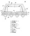
【従来の技術】
半導体装置の小型化のために、近年、BGA型半導体装置が多く用いられている。従来のBGA型半導体装置の構造を図12に示す。半導体チップ41は、インタポーザ基板42上の中心部(内周部)に搭載され、半導体チップ41の裏面がインタポーザ基板42と接着剤43によって固定される。インタポーザ基板42は、ポリイミド、ガラスエポキシ、あるいはBTレジン等の有機性絶縁性材料45から成り、その上に銅等の金属性材料による配線パターン44が設けられている。接着剤43には、熱硬化型のエポキシ系樹脂を主成分とするものが使用される。
【0003】
上記従来のBGA型半導体装置では、インタポーザ基板42が、有機絶縁性材料45と、その上に形成された銅等の金属性材料による接続パッド44とから成る2層構造で構成されているため、インタポーザ基板42を有するBGA型半導体装置の更なる厚みの縮小に障害となっていた。
【0004】
特開平2−240940号公報、10−116935号公報、及び、11−195733号公報には、上記問題を解決するための方法として、樹脂製のインタポーザ基板をその裏面から研磨しその厚みを縮小する技術が記載されている。
【0005】
【発明が解決しようとする課題】
上記各公報に記載の技術では、樹脂製のインタポーザ基板を用い、これを研磨によって除去する構成を採用している。一般にBGA型半導体装置では、ボンディングワイアが接続されるステッチ部の配置が定まると、それに従って外部端子を成す金属バンプの配置がステッチ部の外周側近傍と定まるため、外部端子の配置に自由度がなく、これを搭載する電子部品や電子装置の平面的なサイズの縮小に障害となっていた。
【0006】
特に、近年の電子部品や電子装置のサイズ縮小に伴って、半導体装置の外部端子のピッチについてその縮小の要請が強い。この場合、接続パッドのパターン自体のピッチ縮小は、フォトリソグラフィ技術の進歩によってある程度可能となっているものの、金属バンプの形成には充分なスペースが必要であり、従って、上記外部端子のピッチ縮小の要請には必ずしも応えることが出来なかった。
【0007】
本発明は、上記に鑑み、半導体装置の構造を改良し、特に、厚み及び平面サイズの縮小によってその全体サイズを縮小すること、及び、所望の位置に接続性の良好な配線パターンを形成して外部端子の配置に自由度を持たせることによって、BGA型半導体装置を有する電子部品や電子装置の信頼性の向上、コスト低減及びサイズ縮小を図ることを目的とする。
【0008】
【課題を解決するための手段】
前記目的を達成するため、本発明の第1の視点の半導体装置は、第1の配線パターンと、前記第1の配線パターンの上面及び側面を覆う第1の絶縁層と、該第1の絶縁層上に形成され該第1の絶縁層を貫通するスルーホールを介して前記第1の配線パターンに電気的に接続されたた第2の配線パターンと、前記第1の絶縁層上に搭載された半導体チップと、前記半導体チップに形成されたチップ電極と前記第2の配線パターンとを接続する接続部材と、前記半導体チップ及び接続部材を前記第1の絶縁層上に封止する封止樹脂と、前記第1の配線パターンの下面を覆う第2の絶縁層とを備えることを特徴とする。
【0009】
本発明の半導体装置では、後に除去される基板上に第1の配線パターンが形成され、その上から第1の絶縁層及び第2の配線層が形成され、第1の絶縁層上に搭載される半導体チップのチップ電極は第2の配線パターンと接続されることから、第1の配線パターン自体を外部電極として構成することによって、或いは、第1の配線パターンの下面に外部電極を形成することによって、外部電極の配置は、半導体チップと接続される第2の配線パターンの配置によって制限されない。このため、外部電極の配置に自由度が高まり、半導体装置の設計に自由度が高まる。
【0010】
上記半導体チップのチップ電極と第2の配線パターンとを接続する接続部材は、金属バンプ又は金属ワイアの何れでもよい。
【0011】
また、本発明の第1の視点の半導体装置の製造方法は、金属平板上に第1の配線パターンを形成し、該第1の配線パターンと電気的に接続された第2の配線パターンを、第1の絶縁層を介して前記第1の配線パターン上に形成し、前記第1の絶縁層上に半導体チップを搭載し、該半導体チップのチップ電極と前記第2の配線パターンとを電気的に接続し、前記半導体チップを前記第1の絶縁層上に封止樹脂によって封止し、前記第1の配線パターンを残しつつ前記金属平板を該金属平板の下面から除去し、前記第1の配線パターンの下面に第2の絶縁層を形成することを特徴とする。
【0012】
本発明の第1の視点の半導体装置の製造方法では、第2の配線パターンが半導体チップのチップ電極と接続されるので、第1の配線パターンを外部電極として構成し、或いは、第1の配線パターンの下面に外部電極を接続することにより、半導体チップのチップ電極と外部電極の配置とを独立に配置できるので、双方の電極について配置の自由度が高まる。
【0013】
上記第1の視点の半導体装置の製造方法では、前記第1の配線パターンを、前記金属平板のエッチングによって形成することが好ましい。この場合、必要な部品点数が削減できる。
【0014】
また、前記金属平板の除去は、化学的なエッチング、化学的−機械的な研磨、機械的な研削、又は、機械的な引き剥がしの何れによって行ってもよく、工法の自由度が高い。
【0015】
更に、前記第2の絶縁層を接着性絶縁シートで構成し、この接着性絶縁シートを第1の配線パターン上に貼付してもよい。工程が簡素である。
【0016】
本発明の第2の視点の半導体装置の製造方法は、金属平板の上面に第1の配線パターンを形成すると共に該金属平板の下面にメッキ法によって第2の配線パターンを形成し、前記金属平板上に半導体チップを搭載し、該半導体チップのチップ電極と前記第1の配線パターンとを接続部材によって電気的に接続し、前記半導体チップを前記金属平板上に封止樹脂によって封止し、前記第2の配線パターンをマスクとするパターニングによって前記金属平板を除去し、前記第2の配線パターンの下面に外部電極を形成し、前記外部電極の下面を露出させつつ前記金属平板を除去した部分及び前記第2の配線パターン上に絶縁層を形成することを特徴とする。
【0017】
本半導体の第2の視点の半導体装置の製造方法によると、金属平板を第2の配線パターンと共に残すことにより、半導体装置の剛性が高まる。
【0018】
本発明の第2の視点の半導体装置の製造方法では、半導体チップのチップ電極と第1の配線パターンとを接続する接続部材は、ボンディングワイア又は半田ボールの何れでもよい。また、前記第1の配線パターンもメッキ法によって形成することが出来る。この場合、工程が簡素になる。金属平板を銅によって形成し、第2の配線パターンを金メッキによって形成すると、良好なエッチングマスクが得られる。
【0019】
【発明の実施の形態】
図面を参照して本発明の実施形態例に基づいて本発明を更に詳細に説明する。図1は、本半導体第1の実施形態例の半導体装置の構造を示す断面図である。半導体装置は、第1の配線パターン11と、第1の配線パターン11の上面及び側面を覆う第1の絶縁層12と、第1の絶縁層12上に形成され第1の絶縁層12を貫通するスルーホール13を介して第1の配線パターン11に接続された第2の配線パターン14と、第1の絶縁層12上に搭載された半導体チップ15と、半導体チップ15に形成されたチップ電極16と第2の配線パターン14とを接続するボンディングワイア17と、半導体チップ15及びボンディングワイア17を第1の絶縁層12上に封止する封止樹脂18と、第1の配線パターン11の下面に形成された外部電極を構成する金属バンプ19と、金属バンプ19の下面を露出させつつ第1の配線パターン11の下面を覆う第2の絶縁層を成す接着性絶縁シート20とを備える。
【0020】
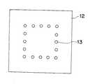
図2に、第1の配線パターンを例示した。第1の配線パターン11は、多数の略多角形のアウターパッド31から構成される。各アウターパッド31には、その上面にスルーホール13が形成され、また、その下面には金属バンプ19が形成される。スルーホール13は、その上層に形成される第2の配線パターンが、半導体チップを搭載する部分を避けて形成されていることから、同様にチップの搭載される位置を避けて配置されている。金属バンプ19は、半導体装置の下面全体にほぼアレイ状に配置される。各アウターパッド31は、スルーホール13と金属バンプ19との間で電気的な導通をとればよいため、その配置に自由度が高い。第1の配線パターン11は、Cu、又は、42アロイ等から形成する。
【0021】
図3及び図4に、第1の絶縁層に形成されるスルーホール13の配置、及び、第2の配線パターン14の配置を夫々示した。第2の配線パターン14は、夫々がボンディングワイアに接続される多数のインナーパッド32と、幾つかのインナーパッド32とスルーホールとを接続する配線部27から構成される。各インナーパッド32は、半導体チップ15が搭載される位置に近接して配置され、スルーホール13に接続される内縁部と、その内縁部から外方向に延長し、ボンディングワイア17に接続されるステッチ部とを有する。
【0022】
図5は、第1の配線パターンの下面に形成される金属バンプの配置を示している。金属バンプは、半導体装置の下面のほぼ全域に亘ってアレイ状に配置される。このようなアレイ状の配置は、半導体チップ15に接続される第2の配線パターン14と、金属バンプ19に接続される第1の配線層11とを分離したことによって得られるものである。このように、金属バンプ19をアレイ状に配置できるので、半導体装置の設計の自由度が向上する。
【0023】
本実施形態例の半導体装置は、半導体チップの下面には、薄い2層の配線パターン11、14及び金属バンプ19が存在するのみであるので、厚み方向の寸法縮小が可能である。
【0024】
なお、ボンディングワイア17は、例えば、Au、Cu、Al、Pdから形成し、接続にあたっては半田や導電ペーストを用いる。また、接着性絶縁シート20には、熱硬化性の高分子材料を用いることが好ましい。
【0025】
図6(a)〜(g)は、本発明の第1の実施形態例の半導体装置の製造工程を順次に示している。この製造方法は、図1の実施形態例の半導体装置の変形例を製造する例であり、本変形例では、第2の配線パターン自体を多層化している。先ず、金属平板(金属フレーム)21の上面にエッチングによって第1の配線パターン11を形成する。
【0026】
第1の配線パターン11を形成した金属平板21上に、ポリイミド又はエポキシ樹脂から成る絶縁基板内に複数の配線層を有する多層配線層23を接着剤22によって貼付する(同図(a))。接着剤22としては熱硬化性の高分子接着剤例えばポリイミドを使用し、温度100〜200℃、押圧力として数十kg/cm2を使用する。これによって、第1の配線パターン12の上面及び側面に接着剤が付着する。
【0027】
次いで、多層配線層をフォトリソグラフィによってパターニングして、第1の配線パターン11上にスルーホール24を形成する(同図(b))。フォトリソグラフィとしては、フォトレジストを塗布する方法や、絶縁フィルムを貼付して露光する方法等が使用される。なお、多層配線層を金属平板21上に貼付する前に、金型やドリルを使用した穴開け加工によって、予め多層配線層にスルーホールを形成しておいてもよい。
【0028】
引き続き、スルーホール24を貫通するボンディングワイア25によって、多層配線層23の外部端子と第1の配線パターン11とを接続する(同図(c))。次いで、半導体チップ15を多層配線層23上に搭載し、半導体チップ15のチップ電極16と、多層配線層23の内部電極とを、ボンディングワイア17によって接続する(同図(d))。
【0029】
次いで、半導体チップ15及びボンディングワイア17、25を封止樹脂18によって封止する(同図(e))。その後、金属平板21の下面から、配線パターン11の部分のみを残して金属平板21を除去する(同図(f))。この除去には、例えば化学的−機械的研磨(CMP)が使用される。次いで、金属平板を除去して露出した第1の配線パターン11の所望部分に、外部電極を成す金属バンプ19を形成する。次いで、第1の配線パターンの下面を第2の絶縁層20によって覆うことによって半導体装置が完成する(同図(g))。
【0030】
上記実施形態例では、第1配線層11上に多層配線層23を貼付することによって、第1の絶縁層12及び第2の配線パターン14を形成する例を挙げたが、これに代えて、金属平板21上に第1の絶縁層12及び第2の配線パターン14を順次に形成してもよい。例えば第1の絶縁層12は、ポリイミド又はエポキシ等の感光性絶縁樹脂材料を、スピンコート法を利用して塗布し、露光及び現像によってスルーホール13を形成する。或いは、通常の絶縁性材料をスピンコート法で塗布し、フォトレジストを利用してエッチングでスルーホール13を形成してもよい。
【0031】
また、スクリーン印刷法を用いて第1の絶縁層12を形成することも出来る。この場合、スルーホール13を形成する部分を覆い、且つ、第1の絶縁層12を形成する部分を開口したスクリーンマスクを第1の配線パターン上に乗せて、ウレタン等の絶縁材料をその上からスキージして金属平板上に付着させ、次いで、これを高温ベークやUV照射によって硬化させる。スクリーンマスクは、例えば金網状の開口部と、金網部分を覆うマスクとから構成する。
【0032】
第2の配線パターン14は、スルーホール13を有する第1の絶縁層12を形成した後に、例えばスパッタ法で形成する。この場合、先ず、第1の絶縁層12上にレジスト層を形成し、その上にスパッタリングで導電層を形成する。露光及び現像によって所望のパターンを、レジスト層及び導電層に形成した後に、電解メッキ法を用いてAl、Ni、Cu等をパターン内に埋め込む。次いで、レジスト層を剥離し、また、スパッタリング法で形成した導電層をエッチングで除去する。
【0033】
第2の配線パターン14の形成は、導電性のペーストを用いてスクリーン印刷法によって形成することも出来る。この場合、導電性ペーストの導電材料としては、AgやCu等を用いる。スクリーン印刷法で導電性ペーストを塗布した後は、高温ベークやUV照射によって樹脂を硬化させる。
【0034】
金属平板21の除去には、化学的−機械的(物理的)な研磨による方法の他に、化学的エッチングによる方法、機械的な研削による方法、機械的な引き剥がしによる方法等が挙げられる。機械的な引き剥がしの方法には、2つの金属層における温度による膨張率の差や一方の金属の高温度での軟化を併せて利用することも考えられる。化学的なエッチングでは、例えば金属平板をCu又は42アロイで形成し、エッチング液としては塩化第2鉄を用いる。機械的な引き剥がし法を用いる場合には、第1の配線パターンを金属平板上にメッキによって形成し、そのメッキの界面から剥がすことが好ましい。
【0035】
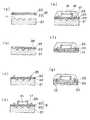
図7は、本発明の第2の実施形態例の半導体装置を示す。本実施形態例は、半導体チップ15のチップ電極16を金属バンプ26によって第2の配線パターン14に形成しており、また、半導体チップ15を封止樹脂18で封止した後に、封止樹脂18及び半導体チップ15の上部を研磨によって除去している点において第1の実施形態例の半導体装置と異なる。
【0036】
図8は、本発明の第3の実施形態例の半導体装置を示す。本実施形態例は、第1の配線パターンをそのまま外部電極として形成した点において、第1の実施形態例と異なる。
【0037】
図9は、本発明の第4の実施形態例の半導体装置を示す。本実施形態例は、半導体チップのチップ電極を金属バンプによって接続した点において、第3の実施形態例と異なる。
【0038】
図10(a)〜(e)は、本発明の第2の実施形態例の半導体装置の製造方法における工程を順次に示している。先ず、Cuから成る金属平板21の上面に、Auから成る第1の配線パターン33を、下面にAuから成る第2の配線パターン34を夫々メッキ法によって形成する(同図(a))。次いで、絶縁性接着剤35を金属平板21の上面に塗布し、半導体チップ15をその上に搭載し接着する。半導体チップ15のチップ電極16と、第1の配線パターン33のステッチ部とをボンディングワイア17によって接続する(同図(b))。引き続き、半導体チップ15及びボンディングワイア17を封止樹脂18によって、金属平板21上に封止する。
【0039】
引き続き、第2の配線パターン34をマスクとして、金属平板21をエッチングし、第2の配線パターン34の上面以外の金属平板21の部分を除去する(同図(d))。更に、第2の配線パターン34の金属バンプ形成位置以外の、半導体装置の下面の全体に絶縁性樹脂を塗布して絶縁層とする。次いで、絶縁層が形成されていない第2の配線パターンの部分に金属バンプを形成する(同図(e))。
【0040】
上記によって得られた半導体装置では、金属平板が第2の配線パターン34の上面に支持構造体として残されており、金属平板21の機械的強度が大きいので、従来のテープ基板を有する半導体装置に比して、全体的な機械的強度が大きい。また、一般に、配線パターン−基材−配線パターンの3相構造を有する従来の半導体装置に比して構成部材が少なくて済む利点がある。また、金属平板21上にメッキ法で予め形成した配線パターン33、34がそのまま最終構造でも配線として機能し、一般にメッキ法で形成する配線パターンはエッチング等により形成する配線パターンに比して精度よく形成できるので、より微細構造の配線パターンが得られる。また、上記実施形態例の製造方法では、スルーホールの形成工程がないので、半導体装置をスループット高く製造できる。
【0041】
特に、第1の配線パターン33を、半導体チップ15のチップ電極16とのボンディングに使用するステッチ部のみに設け、第2の配線パターン34及びその上面の金属平板21を引き回すことにより、外部電極を構成する金属バンプ19の配置に自由度が得られると共に、半導体装置全体の機械的強度が向上する。
【0042】
第1及び第2の配線パターンは、例えば、Ni/Au、Au、Ag、パラジウム、及び、半田メッキによって形成する。
【0043】
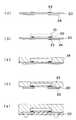
図11(a)〜(e)は、本発明の第3の実施形態例の半導体装置の製造方法の工程を順次に示している。先ず、Cuから成る金属平板21の上面に、Auから成る第1の配線パターン33を、下面にAuから成る第2の配線パターン34を夫々メッキ法によって形成する(同図(a))。次いで、半田バンプから成る金属バンプ26を下面に有する半導体チップ15を、第1の配線パターン上に半田バンプ26を搭載して、導電性接着剤で接着する。(同図(b))。引き続き、半導体チップ15を封止樹脂18によって、金属平板21上に封止する。
【0044】
引き続き、第2の配線パターン34をマスクとして、金属平板21をエッチングし、第2の配線パターン34の上面以外の金属平板21の部分を除去する(同図(d))。更に、第2の配線パターン34の金属バンプ形成位置以外の、半導体装置の下面の全体に絶縁性樹脂を塗布して絶縁層とする。次いで、絶縁層が形成されていない第2の配線パターン34の部分に金属バンプ19を形成する(同図(e))。
【0045】
本実施形態例の製造方法では、第1の配線パターン33は、必要最小限の小さな範囲に形成するのみで足りる。
【0046】
本発明において使用する絶縁層材料としては、ポリイミド、エポキシ、フェノール、シリコーン系樹脂等が挙げられる。また、配線パターンの材料としては、Ni、Cu、Au等が挙げられる。印刷法を利用する場合には、Ag、Cu等を含む導電性ペーストが挙げられる。ボンディングワイアの材料としては、Au、Cu、Al、Pd等が挙げられる。また、金属バンプの材料としては、半田、異方性導電材料、導電ペースト等が挙げられる。また、接着剤としては、熱硬化性の高分子接着剤、例えば、ポリイミド、エポキシ等が挙げられる。
【0047】
以上、本発明をその好適な実施形態例に基づいて説明したが、本発明の樹脂封止型半導体装置及びその製造方法は、上記実施形態例の構成にのみ限定されるものではなく、上記実施形態例の構成から種々の修正及び変更を施したものも、本発明の範囲に含まれる。
【0048】
【発明の効果】
以上説明したように、本発明の樹脂封止型半導体装置によると、外部端子の配置に自由度が高まるので、半導体装置全体の厚み方向及び平面方向のサイズの縮小、並びに、そのコストの低減が可能であるという顕著な効果を奏する。
【図面の簡単な説明】
【図1】本発明の一実施形態例の半導体装置の断面図。
【図2】図1における第1の配線パターンの平面図。
【図3】図1における第1の絶縁層のスルーホールを示す平面図。
【図4】図1における第2の配線パターンの平面図。
【図5】図1における金属バンプの配置平面図。
【図6】本発明の一実施形態例の半導体装置の製造法を順次に示す断面図。
【図7】本発明の第2の実施形態例の半導体装置断面図。
【図8】本発明の第3の実施形態例の半導体装置の断面図。
【図9】本発明の第4の実施形態例の半導体装置の断面図。
【図10】本発明の第2の実施形態例の半導体装置の製造方法を順次に示す断面図。
【図11】本発明の第3の実施形態例の半導体装置の製造方法を順次に示す断面図。
【図12】従来の樹脂封止型半導体装置の断面図。
【符号の説明】
11:第1の配線パターン
12:第1の絶縁層
13:スルーホール
14:第2の配線パターン
15:半導体チップ
16:チップ電極
17:ボンディングワイア
18:封止樹脂
19:金属バンプ
20:第2の絶縁層
21:金属平板
22:接着層
23:多層配線層
24:スルーホール
25:ボンディングワイア
26:金属バンプ
27:パッド配線部
31:アウターパッド
32:インナーパッド
33:第1の配線パターン
34:第2の配線パターン[0001]
BACKGROUND OF THE INVENTION
The present invention relates to a semiconductor device and a manufacturing method thereof, and more particularly to a structure and manufacturing method of a semiconductor device suitable for size reduction in a thickness direction and a planar direction of the semiconductor device.
[0002]
[Prior art]
In recent years, many BGA type semiconductor devices are used for miniaturization of semiconductor devices. The structure of a conventional BGA type semiconductor device is shown in FIG. The
[0003]
In the above-described conventional BGA type semiconductor device, the
[0004]
In JP-A-2-240940, 10-116935, and 11-195733, as a method for solving the above problem, a resin-made interposer substrate is polished from its back surface to reduce its thickness. The technology is described.
[0005]
[Problems to be solved by the invention]
The technology described in each of the above publications employs a configuration in which a resin interposer substrate is used and removed by polishing. In general, in the BGA type semiconductor device, when the arrangement of the stitch portion to which the bonding wire is connected is determined, the arrangement of the metal bumps constituting the external terminal is determined in the vicinity of the outer peripheral side of the stitch portion, and thus the degree of freedom in the arrangement of the external terminal is increased. However, it has been an obstacle to reducing the planar size of electronic components and electronic devices on which they are mounted.
[0006]
In particular, with the recent reduction in size of electronic components and electronic devices, there is a strong demand for reducing the pitch of external terminals of semiconductor devices. In this case, although the pitch of the connection pad pattern itself can be reduced to some extent by the advancement of photolithography technology, a sufficient space is required for forming the metal bumps. The request could not always be met.
[0007]
In view of the above, the present invention improves the structure of a semiconductor device, particularly reduces the overall size by reducing the thickness and planar size, and forms a wiring pattern with good connectivity at a desired position. It is an object of the present invention to improve the reliability, cost reduction, and size reduction of electronic components and electronic devices having a BGA type semiconductor device by providing flexibility in the arrangement of external terminals.
[0008]
[Means for Solving the Problems]
In order to achieve the above object, a semiconductor device according to a first aspect of the present invention includes a first wiring pattern, a first insulating layer covering an upper surface and a side surface of the first wiring pattern, and the first insulation. A second wiring pattern formed on the layer and electrically connected to the first wiring pattern through a through-hole penetrating the first insulating layer; and mounted on the first insulating layer. A semiconductor chip, a connection member for connecting the chip electrode formed on the semiconductor chip and the second wiring pattern, and a sealing resin for sealing the semiconductor chip and the connection member on the first insulating layer And a second insulating layer covering the lower surface of the first wiring pattern.
[0009]
In the semiconductor device of the present invention, a first wiring pattern is formed on a substrate to be removed later, and a first insulating layer and a second wiring layer are formed thereon and mounted on the first insulating layer. Since the chip electrode of the semiconductor chip is connected to the second wiring pattern, the first wiring pattern itself is configured as an external electrode, or the external electrode is formed on the lower surface of the first wiring pattern. Therefore, the arrangement of the external electrodes is not limited by the arrangement of the second wiring pattern connected to the semiconductor chip. For this reason, the degree of freedom increases in the arrangement of the external electrodes, and the degree of freedom in designing the semiconductor device increases.
[0010]
The connection member that connects the chip electrode of the semiconductor chip and the second wiring pattern may be either a metal bump or a metal wire.
[0011]
According to the first aspect of the present invention, there is provided a method for manufacturing a semiconductor device, wherein a first wiring pattern is formed on a metal flat plate, and a second wiring pattern electrically connected to the first wiring pattern is obtained. Formed on the first wiring pattern through a first insulating layer, a semiconductor chip is mounted on the first insulating layer, and the chip electrode of the semiconductor chip and the second wiring pattern are electrically connected The semiconductor chip is sealed on the first insulating layer with a sealing resin, and the metal flat plate is removed from the lower surface of the metal flat plate while leaving the first wiring pattern. A second insulating layer is formed on the lower surface of the wiring pattern.
[0012]
In the method of manufacturing a semiconductor device according to the first aspect of the present invention, the second wiring pattern is connected to the chip electrode of the semiconductor chip. Therefore, the first wiring pattern is configured as an external electrode, or the first wiring By connecting an external electrode to the lower surface of the pattern, the chip electrode of the semiconductor chip and the arrangement of the external electrode can be arranged independently, so that the degree of freedom of arrangement of both electrodes is increased.
[0013]
In the semiconductor device manufacturing method of the first aspect, it is preferable that the first wiring pattern is formed by etching the metal flat plate. In this case, the number of necessary parts can be reduced.
[0014]
Further, the removal of the metal flat plate may be performed by any of chemical etching, chemical-mechanical polishing, mechanical grinding, or mechanical peeling, and the degree of freedom of the construction method is high.
[0015]
Furthermore, the second insulating layer may be composed of an adhesive insulating sheet, and the adhesive insulating sheet may be affixed on the first wiring pattern. The process is simple.
[0016]
According to a second aspect of the present invention, there is provided a method of manufacturing a semiconductor device, wherein a first wiring pattern is formed on an upper surface of a metal flat plate, and a second wiring pattern is formed on the lower surface of the metal flat plate by a plating method. A semiconductor chip is mounted thereon, the chip electrode of the semiconductor chip and the first wiring pattern are electrically connected by a connecting member, the semiconductor chip is sealed on the metal flat plate with a sealing resin, The metal flat plate is removed by patterning using the second wiring pattern as a mask, an external electrode is formed on the lower surface of the second wiring pattern, and the metal flat plate is removed while exposing the lower surface of the external electrode; An insulating layer is formed on the second wiring pattern.
[0017]
According to the semiconductor device manufacturing method of the second aspect of the present semiconductor, the rigidity of the semiconductor device is increased by leaving the metal flat plate together with the second wiring pattern.
[0018]
In the method of manufacturing a semiconductor device according to the second aspect of the present invention, the connecting member that connects the chip electrode of the semiconductor chip and the first wiring pattern may be either a bonding wire or a solder ball. The first wiring pattern can also be formed by a plating method. In this case, the process is simplified. When the metal flat plate is formed of copper and the second wiring pattern is formed of gold plating, a good etching mask can be obtained.
[0019]
DETAILED DESCRIPTION OF THE INVENTION
The present invention will be described in more detail based on exemplary embodiments of the present invention with reference to the drawings. FIG. 1 is a cross-sectional view showing the structure of the semiconductor device of the first embodiment of the semiconductor. The semiconductor device includes a
[0020]
FIG. 2 illustrates the first wiring pattern. The
[0021]
3 and 4 show the arrangement of the through
[0022]
FIG. 5 shows an arrangement of metal bumps formed on the lower surface of the first wiring pattern. The metal bumps are arranged in an array over almost the entire lower surface of the semiconductor device. Such an array-like arrangement is obtained by separating the
[0023]
In the semiconductor device of this embodiment example, the thin two-
[0024]
The
[0025]
6A to 6G sequentially show the manufacturing steps of the semiconductor device according to the first embodiment of the present invention. This manufacturing method is an example of manufacturing a modified example of the semiconductor device of the embodiment of FIG. 1, and in this modified example, the second wiring pattern itself is multilayered. First, the
[0026]
On the metal
[0027]
Next, the multilayer wiring layer is patterned by photolithography to form a through
[0028]
Subsequently, an external terminal of the
[0029]
Next, the
[0030]
In the above embodiment, the example in which the first insulating
[0031]
Alternatively, the first insulating
[0032]
The
[0033]
The
[0034]
The removal of the metal
[0035]
FIG. 7 shows a semiconductor device according to the second embodiment of the present invention. In this embodiment, the
[0036]
FIG. 8 shows a semiconductor device according to a third embodiment of the present invention. This embodiment differs from the first embodiment in that the first wiring pattern is formed as an external electrode as it is.
[0037]
FIG. 9 shows a semiconductor device according to a fourth embodiment of the present invention. This embodiment differs from the third embodiment in that the chip electrodes of the semiconductor chip are connected by metal bumps.
[0038]
FIGS. 10A to 10E sequentially show the steps in the method for manufacturing the semiconductor device according to the second embodiment of the present invention. First, a
[0039]
Subsequently, using the
[0040]
In the semiconductor device obtained as described above, the metal flat plate is left as a support structure on the upper surface of the
[0041]
In particular, the
[0042]
The first and second wiring patterns are formed by, for example, Ni / Au, Au, Ag, palladium, and solder plating.
[0043]
11A to 11E sequentially show the steps of the semiconductor device manufacturing method according to the third embodiment of the present invention. First, a
[0044]
Subsequently, using the
[0045]
In the manufacturing method of the present embodiment example, it is sufficient to form the
[0046]
Examples of the insulating layer material used in the present invention include polyimide, epoxy, phenol, and silicone resin. Moreover, Ni, Cu, Au etc. are mentioned as a material of a wiring pattern. When the printing method is used, a conductive paste containing Ag, Cu, or the like can be given. Examples of the bonding wire material include Au, Cu, Al, and Pd. Examples of the metal bump material include solder, anisotropic conductive material, and conductive paste. Examples of the adhesive include thermosetting polymer adhesives such as polyimide and epoxy.
[0047]
As described above, the present invention has been described based on the preferred embodiment. However, the resin-encapsulated semiconductor device and the manufacturing method thereof according to the present invention are not limited to the configuration of the above-described embodiment. A configuration in which various modifications and changes are made from the configuration of the embodiment is also included in the scope of the present invention.
[0048]
【The invention's effect】
As described above, according to the resin-encapsulated semiconductor device of the present invention, the degree of freedom in the arrangement of the external terminals is increased. There is a remarkable effect that it is possible.
[Brief description of the drawings]
FIG. 1 is a cross-sectional view of a semiconductor device according to an embodiment of the present invention.
FIG. 2 is a plan view of a first wiring pattern in FIG.
3 is a plan view showing a through hole of the first insulating layer in FIG. 1. FIG.
4 is a plan view of a second wiring pattern in FIG. 1. FIG.
5 is an arrangement plan view of metal bumps in FIG. 1. FIG.
6 is a cross-sectional view sequentially showing a method for manufacturing a semiconductor device according to an embodiment of the present invention. FIG.
FIG. 7 is a sectional view of a semiconductor device according to a second embodiment of the present invention.
FIG. 8 is a cross-sectional view of a semiconductor device according to a third embodiment of the present invention.
FIG. 9 is a sectional view of a semiconductor device according to a fourth embodiment of the present invention.
FIG. 10 is a cross-sectional view sequentially showing a method for manufacturing a semiconductor device according to a second embodiment of the present invention.
FIG. 11 is a cross-sectional view sequentially showing a method for manufacturing a semiconductor device according to a third embodiment of the present invention.
FIG. 12 is a cross-sectional view of a conventional resin-encapsulated semiconductor device.
[Explanation of symbols]
11: first wiring pattern 12: first insulating layer 13: through hole 14: second wiring pattern 15: semiconductor chip 16: chip electrode 17: bonding wire 18: sealing resin 19: metal bump 20: second Insulating layer 21: Metal flat plate 22: Adhesive layer 23: Multilayer wiring layer 24: Through hole 25: Bonding wire 26: Metal bump 27: Pad wiring portion 31: Outer pad 32: Inner pad 33: First wiring pattern 34: Second wiring pattern
Claims (6)
Translated fromJapanesePriority Applications (5)
| Application Number | Priority Date | Filing Date | Title |
|---|---|---|---|
| JP2000258423AJP4454814B2 (en) | 2000-08-29 | 2000-08-29 | Resin-sealed semiconductor device and manufacturing method thereof |
| US09/940,249US20030107129A1 (en) | 2000-08-29 | 2001-08-27 | Resin encapsulated BGA-type semiconductor device |
| TW90121129ATW531818B (en) | 2000-08-29 | 2001-08-28 | Resin encapsulated BGA-type semiconductor device |
| KR10-2001-0052507AKR100442911B1 (en) | 2000-08-29 | 2001-08-29 | Resin encapsulated bga-type semiconductor device and method for manufacturing the same |
| US10/412,001US20030166314A1 (en) | 2000-08-29 | 2003-04-11 | Resin encapsulated BGA-type semiconductor device |
Applications Claiming Priority (1)
| Application Number | Priority Date | Filing Date | Title |
|---|---|---|---|
| JP2000258423AJP4454814B2 (en) | 2000-08-29 | 2000-08-29 | Resin-sealed semiconductor device and manufacturing method thereof |
Publications (2)
| Publication Number | Publication Date |
|---|---|
| JP2002076166A JP2002076166A (en) | 2002-03-15 |
| JP4454814B2true JP4454814B2 (en) | 2010-04-21 |
Family
ID=18746739
Family Applications (1)
| Application Number | Title | Priority Date | Filing Date |
|---|---|---|---|
| JP2000258423AExpired - Fee RelatedJP4454814B2 (en) | 2000-08-29 | 2000-08-29 | Resin-sealed semiconductor device and manufacturing method thereof |
Country Status (4)
| Country | Link |
|---|---|
| US (2) | US20030107129A1 (en) |
| JP (1) | JP4454814B2 (en) |
| KR (1) | KR100442911B1 (en) |
| TW (1) | TW531818B (en) |
Families Citing this family (8)
| Publication number | Priority date | Publication date | Assignee | Title |
|---|---|---|---|---|
| JP2003338587A (en)* | 2002-05-21 | 2003-11-28 | Hitachi Ltd | Semiconductor device and manufacturing method thereof |
| TWI298939B (en)* | 2003-04-18 | 2008-07-11 | Advanced Semiconductor Eng | Stack-type multi-chips package |
| CN100442495C (en)* | 2005-10-12 | 2008-12-10 | 南茂科技股份有限公司 | Flexible Substrates for Packaging |
| US8310040B2 (en)* | 2010-12-08 | 2012-11-13 | General Electric Company | Semiconductor device package having high breakdown voltage and low parasitic inductance and method of manufacturing thereof |
| US9735120B2 (en)* | 2013-12-23 | 2017-08-15 | Intel Corporation | Low z-height package assembly |
| US9406531B1 (en) | 2014-03-28 | 2016-08-02 | STATS ChipPAC Pte. Ltd. | Integrated circuit packaging system with photoimagable dielectric-defined trace and method of manufacture thereof |
| US9947553B2 (en)* | 2015-01-16 | 2018-04-17 | Rohm Co., Ltd. | Manufacturing method of semiconductor device and semiconductor device |
| JP7255788B2 (en)* | 2018-04-04 | 2023-04-11 | 住友電工プリントサーキット株式会社 | Cover film for flexible printed wiring board and flexible printed wiring board |
Family Cites Families (18)
| Publication number | Priority date | Publication date | Assignee | Title |
|---|---|---|---|---|
| KR100280762B1 (en)* | 1992-11-03 | 2001-03-02 | 비센트 비.인그라시아 | Thermally Reinforced Semiconductor Devices Having Exposed Backsides and Methods of Manufacturing the Same |
| WO2004093183A1 (en)* | 1995-03-17 | 2004-10-28 | Atsushi Hino | Film carrier and semiconductor device using the same |
| JPH08288424A (en)* | 1995-04-18 | 1996-11-01 | Nec Corp | Semiconductor device |
| US5634268A (en)* | 1995-06-07 | 1997-06-03 | International Business Machines Corporation | Method for making direct chip attach circuit card |
| JP3248149B2 (en)* | 1995-11-21 | 2002-01-21 | シャープ株式会社 | Resin-sealed semiconductor device and method of manufacturing the same |
| US5710071A (en)* | 1995-12-04 | 1998-01-20 | Motorola, Inc. | Process for underfilling a flip-chip semiconductor device |
| KR100274333B1 (en)* | 1996-01-19 | 2001-01-15 | 모기 쥰이찌 | conductive layer adhesive anisotropic concuctive sheet and wiring board using such a sheet |
| JPH104151A (en)* | 1996-06-17 | 1998-01-06 | Citizen Watch Co Ltd | Semiconductor device and its manufacture |
| JPH1084014A (en)* | 1996-07-19 | 1998-03-31 | Shinko Electric Ind Co Ltd | Manufacture of semiconductor device |
| US5759737A (en)* | 1996-09-06 | 1998-06-02 | International Business Machines Corporation | Method of making a component carrier |
| US5863812A (en)* | 1996-09-19 | 1999-01-26 | Vlsi Technology, Inc. | Process for manufacturing a multi layer bumped semiconductor device |
| JPH1154646A (en)* | 1997-07-31 | 1999-02-26 | Toshiba Corp | Semiconductor device package and method of manufacturing the same |
| US6137164A (en)* | 1998-03-16 | 2000-10-24 | Texas Instruments Incorporated | Thin stacked integrated circuit device |
| US6365978B1 (en)* | 1999-04-02 | 2002-04-02 | Texas Instruments Incorporated | Electrical redundancy for improved mechanical reliability in ball grid array packages |
| JP2000340737A (en)* | 1999-05-31 | 2000-12-08 | Mitsubishi Electric Corp | Semiconductor package and its package |
| US6228687B1 (en)* | 1999-06-28 | 2001-05-08 | Micron Technology, Inc. | Wafer-level package and methods of fabricating |
| US6617681B1 (en)* | 1999-06-28 | 2003-09-09 | Intel Corporation | Interposer and method of making same |
| JP3213291B2 (en)* | 1999-06-29 | 2001-10-02 | ソニーケミカル株式会社 | Multilayer substrate and semiconductor device |
- 2000
- 2000-08-29JPJP2000258423Apatent/JP4454814B2/ennot_activeExpired - Fee Related
- 2001
- 2001-08-27USUS09/940,249patent/US20030107129A1/ennot_activeAbandoned
- 2001-08-28TWTW90121129Apatent/TW531818B/ennot_activeIP Right Cessation
- 2001-08-29KRKR10-2001-0052507Apatent/KR100442911B1/ennot_activeExpired - Fee Related
- 2003
- 2003-04-11USUS10/412,001patent/US20030166314A1/ennot_activeAbandoned
Also Published As
| Publication number | Publication date |
|---|---|
| KR20020018116A (en) | 2002-03-07 |
| KR100442911B1 (en) | 2004-08-02 |
| US20030166314A1 (en) | 2003-09-04 |
| JP2002076166A (en) | 2002-03-15 |
| US20030107129A1 (en) | 2003-06-12 |
| TW531818B (en) | 2003-05-11 |
Similar Documents
| Publication | Publication Date | Title |
|---|---|---|
| JP3925809B2 (en) | Semiconductor device and manufacturing method thereof | |
| KR100383112B1 (en) | Resin-encapsulated semiconductor device | |
| KR100838440B1 (en) | Electronic device substrate and its manufacturing method, and Electronic device and its manufacturing method | |
| JP4431123B2 (en) | Electronic device substrate and manufacturing method thereof, and electronic device and manufacturing method thereof | |
| JP4400802B2 (en) | Lead frame, manufacturing method thereof, and semiconductor device | |
| TWI278048B (en) | Semiconductor device and its manufacturing method | |
| JP3888854B2 (en) | Manufacturing method of semiconductor integrated circuit | |
| JP4052915B2 (en) | Circuit device manufacturing method | |
| JP2005294451A (en) | Semiconductor integrated circuit manufacturing method, semiconductor integrated circuit, and semiconductor integrated circuit device | |
| JP2001110831A (en) | External connection projection and method of forming the same, semiconductor chip, circuit board, and electronic device | |
| JP2004119726A (en) | Method of manufacturing circuit device | |
| US20020190377A1 (en) | Circuit device and method for fabricating the same | |
| JP4446772B2 (en) | Circuit device and manufacturing method thereof | |
| JP2004119727A (en) | Method of manufacturing circuit device | |
| JP4454814B2 (en) | Resin-sealed semiconductor device and manufacturing method thereof | |
| US20040106288A1 (en) | Method for manufacturing circuit devices | |
| JP2003007916A (en) | Method of manufacturing circuit device | |
| JP2003007917A (en) | Method manufacturing circuit device | |
| US8062927B2 (en) | Wiring board and method of manufacturing the same, and electronic component device using the wiring board and method of manufacturing the same | |
| JP2004193297A (en) | Wafer level package and method of manufacturing the same | |
| TWI420610B (en) | Semiconductor device and manufacturing method therefor | |
| JP2001250876A (en) | Semiconductor device and its manufacturing method | |
| JP4759981B2 (en) | Manufacturing method of electronic component built-in module | |
| JP2007158069A (en) | External connection structure for semiconductor package and manufacturing method thereof | |
| JP4330855B2 (en) | Wiring board manufacturing method |
Legal Events
| Date | Code | Title | Description |
|---|---|---|---|
| A621 | Written request for application examination | Free format text:JAPANESE INTERMEDIATE CODE: A621 Effective date:20070712 | |
| A977 | Report on retrieval | Free format text:JAPANESE INTERMEDIATE CODE: A971007 Effective date:20090630 | |
| A131 | Notification of reasons for refusal | Free format text:JAPANESE INTERMEDIATE CODE: A131 Effective date:20090702 | |
| A521 | Request for written amendment filed | Free format text:JAPANESE INTERMEDIATE CODE: A523 Effective date:20090828 | |
| A131 | Notification of reasons for refusal | Free format text:JAPANESE INTERMEDIATE CODE: A131 Effective date:20090928 | |
| A521 | Request for written amendment filed | Free format text:JAPANESE INTERMEDIATE CODE: A523 Effective date:20091127 | |
| TRDD | Decision of grant or rejection written | ||
| A01 | Written decision to grant a patent or to grant a registration (utility model) | Free format text:JAPANESE INTERMEDIATE CODE: A01 Effective date:20100105 | |
| A01 | Written decision to grant a patent or to grant a registration (utility model) | Free format text:JAPANESE INTERMEDIATE CODE: A01 | |
| A61 | First payment of annual fees (during grant procedure) | Free format text:JAPANESE INTERMEDIATE CODE: A61 Effective date:20100203 | |
| FPAY | Renewal fee payment (event date is renewal date of database) | Free format text:PAYMENT UNTIL: 20130212 Year of fee payment:3 | |
| R150 | Certificate of patent or registration of utility model | Free format text:JAPANESE INTERMEDIATE CODE: R150 | |
| FPAY | Renewal fee payment (event date is renewal date of database) | Free format text:PAYMENT UNTIL: 20130212 Year of fee payment:3 | |
| S533 | Written request for registration of change of name | Free format text:JAPANESE INTERMEDIATE CODE: R313533 | |
| R350 | Written notification of registration of transfer | Free format text:JAPANESE INTERMEDIATE CODE: R350 | |
| FPAY | Renewal fee payment (event date is renewal date of database) | Free format text:PAYMENT UNTIL: 20130212 Year of fee payment:3 | |
| FPAY | Renewal fee payment (event date is renewal date of database) | Free format text:PAYMENT UNTIL: 20140212 Year of fee payment:4 | |
| LAPS | Cancellation because of no payment of annual fees |