JP4454718B2 - Plasma processing apparatus and electrodes used therefor - Google Patents
Plasma processing apparatus and electrodes used thereforDownload PDFInfo
- Publication number
- JP4454718B2 JP4454718B2JP12687899AJP12687899AJP4454718B2JP 4454718 B2JP4454718 B2JP 4454718B2JP 12687899 AJP12687899 AJP 12687899AJP 12687899 AJP12687899 AJP 12687899AJP 4454718 B2JP4454718 B2JP 4454718B2
- Authority
- JP
- Japan
- Prior art keywords
- electrode
- plasma
- plasma processing
- electrode plate
- central portion
- Prior art date
- Legal status (The legal status is an assumption and is not a legal conclusion. Google has not performed a legal analysis and makes no representation as to the accuracy of the status listed.)
- Expired - Lifetime
Links
- 238000012545processingMethods0.000titleclaimsdescription130
- 230000005684electric fieldEffects0.000claimsdescription57
- 239000000758substrateSubstances0.000claimsdescription45
- 239000004065semiconductorSubstances0.000claimsdescription39
- 239000004020conductorSubstances0.000claimsdescription32
- 230000000694effectsEffects0.000claimsdescription13
- 238000010521absorption reactionMethods0.000claimsdescription12
- 230000035699permeabilityEffects0.000claimsdescription9
- 239000002019doping agentSubstances0.000claimsdescription7
- 239000007789gasSubstances0.000description48
- 238000005530etchingMethods0.000description16
- 238000009826distributionMethods0.000description14
- 230000008859changeEffects0.000description7
- 239000000463materialSubstances0.000description7
- 238000000034methodMethods0.000description5
- 239000003507refrigerantSubstances0.000description4
- ZOXJGFHDIHLPTG-UHFFFAOYSA-NBoronChemical compound[B]ZOXJGFHDIHLPTG-UHFFFAOYSA-N0.000description3
- 229910052796boronInorganic materials0.000description3
- 238000005229chemical vapour depositionMethods0.000description3
- 230000007423decreaseEffects0.000description3
- 238000013461designMethods0.000description3
- IJGRMHOSHXDMSA-UHFFFAOYSA-NAtomic nitrogenChemical compoundN#NIJGRMHOSHXDMSA-UHFFFAOYSA-N0.000description2
- XAGFODPZIPBFFR-UHFFFAOYSA-NaluminiumChemical compound[Al]XAGFODPZIPBFFR-UHFFFAOYSA-N0.000description2
- 229910052782aluminiumInorganic materials0.000description2
- 239000000919ceramicSubstances0.000description2
- 239000003989dielectric materialSubstances0.000description2
- 239000011810insulating materialSubstances0.000description2
- 150000002500ionsChemical class0.000description2
- 229920001721polyimidePolymers0.000description2
- 239000009719polyimide resinSubstances0.000description2
- 238000004544sputter depositionMethods0.000description2
- 238000012546transferMethods0.000description2
- 239000002023woodSubstances0.000description2
- 230000009471actionEffects0.000description1
- 230000015572biosynthetic processEffects0.000description1
- 239000003990capacitorSubstances0.000description1
- 238000001816coolingMethods0.000description1
- 238000010586diagramMethods0.000description1
- 238000010494dissociation reactionMethods0.000description1
- 230000005593dissociationsEffects0.000description1
- 230000002500effect on skinEffects0.000description1
- 239000007772electrode materialSubstances0.000description1
- NBVXSUQYWXRMNV-UHFFFAOYSA-NfluoromethaneChemical compoundFCNBVXSUQYWXRMNV-UHFFFAOYSA-N0.000description1
- 229910052736halogenInorganic materials0.000description1
- 150000002367halogensChemical class0.000description1
- 239000007788liquidSubstances0.000description1
- 238000004519manufacturing processMethods0.000description1
- 230000007246mechanismEffects0.000description1
- 238000012986modificationMethods0.000description1
- 230000004048modificationEffects0.000description1
- 229910052757nitrogenInorganic materials0.000description1
- 229910052756noble gasInorganic materials0.000description1
- 150000002835noble gasesChemical class0.000description1
- 230000002093peripheral effectEffects0.000description1
- 229910052710siliconInorganic materials0.000description1
- 239000010703siliconSubstances0.000description1
- 238000001179sorption measurementMethods0.000description1
- 238000005507sprayingMethods0.000description1
- 229910000859α-FeInorganic materials0.000description1
Images


Landscapes
- Plasma Technology (AREA)
- Physical Vapour Deposition (AREA)
- ing And Chemical Polishing (AREA)
- Drying Of Semiconductors (AREA)
Description
Translated fromJapanese【0001】
【発明の属する技術分野】
本発明は、半導体基板等の基板にプラズマ処理を施すプラズマ処理装置およびそれに用いられる電極に関する。
【0002】
【従来の技術】
例えば半導体デバイスの製造プロセスにおいては、被処理基板である半導体ウエハに対して、エッチングやスパッタリング、CVD(化学気相成長)等のプラズマ処理が多用されている。
【0003】
このようなプラズマ処理を行うためのプラズマ処理装置としては、種々のものが用いられているが、その中でも容量結合型平行平板プラズマ処理装置が主流である。
【0004】
容量結合型平行平板プラズマ処理装置は、チャンバー内に一対の平行平板電極(上部および下部電極)を配置し、処理ガスをチャンバー内に導入するとともに、電極の少なくとも一方に高周波を印加して電極間に高周波電界を形成し、この高周波電界により処理ガスのプラズマを形成して半導体ウエハに対してプラズマ処理を施す。
【0005】
このような容量結合型平行平板プラズマ処理装置により半導体ウエハ上の膜、例えば酸化膜をエッチングする場合には、チャンバー内を中圧にして、中密度プラズマを形成することにより、最適ラジカル制御が可能であり、それによって適切なプラズマ状態を得ることができ、高い選択比で、安定性および再現性の高いエッチングを実現している。
【0006】
しかしながら、近年、USLIにおけるデザインルールの微細化がますます進み、ホール形状のアスペクト比もより高いものが要求されており、酸化膜のエッチング等において従来の条件では必ずしも十分とはいえなくなりつつある。
【0007】
そこで、印加する高周波電力の周波数を上昇させ、良好なプラズマの解離状態を維持しつつ、高密度プラズマを形成することが試みられている。これにより、より低圧の条件下で適切なプラズマを形成することができるので、さらなるデザインルールの微細化に適切に対応することが可能となる。
【0008】
【発明が解決しようとする課題】
ところで、本発明者の検討結果によれば、このようなプラズマ処理装置においては、上部電極が導電体または半導体であるため、以下のような不都合が生じることが判明した。
【0009】
上述したように高密度プラズマを形成するために印加周波数を上昇させると、高周波が印加される電極における表面のインダクタンスを無視することができなくなり、径方向での電界分布が不均一になる。
【0010】
また、このようにプラズマを高密度化するとプラズマの非線形性の特性が顕著に現れ、プラズマからの反射波の高調波が増加する。そして、電極径がφ250〜φ300となると、このような高調波により電極表面に定在波が生成され、やはり電極表面の電界分布が不均一になる。
【0011】
このように電界分布が不均一になるとプラズマ密度が不均一となってエッチングレート分布が不均一となるため、上記いずれかの電界分布不均一の原因を取り除いてエッチングレート分布を均一にすることが必要となる。
【0012】
しかしながら、従来、このような高密度プラズマを用いた場合の問題点が必ずしも明確に認識されていたわけではなく、上記のような電界分布不均一を解消しようとする試みは未だなされていない。
【0013】
本発明はかかる事情に鑑みてなされたものであって、より微細化に対応可能な高密度プラズマを用いたプラズマ処理において、電極表面における電界分布の不均一を小さくすることが可能なプラズマ処理装置およびそれに用いられる電極を提供することを目的とする。
【0014】
【課題を解決するための手段】
上記課題を解決するために、本発明の第1の観点によれば、チャンバー内に第1および第2の電極を互いに平行に設け、前記第2の電極に被処理基板を支持させた状態で、減圧下に保持されたチャンバー内に処理ガスを導入しつつ上記第1および第2の電極間に高周波電界を形成して処理ガスのプラズマを生成し、このプラズマにより被処理基板に所定のプラズマ処理を施すプラズマ処理装置であって、
前記第1の電極は、第2の電極に対向するように設けられた電極板を備え、この電極板は、導電体または半導体で構成された外側部分と、誘電体部材で構成された中央部分とを有し、前記電極板の前記第2電極側の面は、前記外側部分と前記中央部分とが平らになるように形成され、前記第1の電極には、その前記第2の電極と反対側の面から高周波電力が印加されることを特徴とするプラズマ処理装置が提供される。
前記誘電体部材からなる前記中央部分の直径は10〜50mmであることが好ましい。
【0015】
本発明の第2の観点によれば、チャンバー内に第1および第2の電極を互いに平行に設け、前記第2の電極に被処理基板を支持させた状態で、減圧下に保持されたチャンバー内に処理ガスを導入しつつ上記第1および第2の電極間に高周波電界を形成して処理ガスのプラズマを生成し、このプラズマにより被処理基板に所定のプラズマ処理を施すプラズマ処理装置であって、
前記第1の電極は、第2の電極に対向するように設けられた電極板を備え、この電極板は、導電体または半導体で構成された外側部分と、高抵抗部材で構成された中央部分とを有し、前記電極板の前記第2電極側の面は、前記外側部分と前記中央部分とが平らになるように形成され、前記第1の電極には、その前記第2の電極と反対側の面から高周波電力が印加されることを特徴とするプラズマ処理装置が形成される。
前記高抵抗部材からなる前記中央部分の直径は50〜220mmであることが好ましい。
【0016】
上記第1および第2の観点において前記高抵抗部材からなる前記中央部分の以下の(1)式で表されるスキンデップスδが、前記電極板の前記中央部分の厚さよりも大きいことが好ましい。
δ=(2/ωσμ)1/2 ……(1)
ただし、ω=2πf(f:周波数)、σ:導電率、μ:透磁率
また、前記電極板の前記外側部分および前記中央部分がいずれもSiからなり、ドーパントのドープ量を異ならせることにより前記外側部分と前記中央部分とを形成することが好ましい。
【0017】
本発明の第3の観点によれば、チャンバー内に第1および第2の電極を互いに平行に設け、前記第2の電極に被処理基板を支持させた状態で、減圧下に保持されたチャンバー内に処理ガスを導入しつつ上記第1および第2の電極間に高周波電界を形成して処理ガスのプラズマを生成し、このプラズマにより被処理基板に所定のプラズマ処理を施すプラズマ処理装置であって、
前記第1の電極は、第2の電極に対向するように設けられた、導電体または半導体で構成された電極板を備え、誘電体部材がこの電極板の第2の電極側と反対側の面の中央部に接するように設けられ、前記第1の電極には、その前記第2の電極と反対側の面から高周波電力が印加されることを特徴とするプラズマ処理装置が提供される。
【0018】
本発明の第4の観点によれば、チャンバー内に第1および第2の電極を互いに平行に設け、前記第2の電極に被処理基板を支持させた状態で、減圧下に保持されたチャンバー内に処理ガスを導入しつつ上記第1および第2の電極間に高周波電界を形成して処理ガスのプラズマを生成し、このプラズマにより被処理基板に所定のプラズマ処理を施すプラズマ処理装置であって、
前記第1の電極は、第2の電極に対向するように設けられた、導電体または半導体で構成された電極板を備え、高抵抗部材がこの電極板の第2の電極側と反対側の面の中央部に接するように設けられ、前記第1の電極には、その前記第2の電極と反対側の面から高周波電力が印加されることを特徴とするプラズマ処理装置が提供される。
【0019】
上記第3および第4の観点において、前記電極板は、以下の(1)式で表されるスキンデップスδが、電極板の厚さよりも大きいことが好ましい。
δ=(2/ωσμ)1/2 ……(1)
ただし、ω=2πf(f:周波数)、σ:導電率、μ:透磁率
また、前記誘電体部材または前記高抵抗部材の直径は50〜220mmであることが好ましい。
さらに、前記電極板の抵抗は1〜100Ω・cmであることが好ましい。
さらにまた、前記誘電体部材または前記高抵抗部材の全体は、前記電極板と電極支持体とで覆われていることが好ましい。
さらにまた、電極支持体にはガス供給管が接続され、前記電極板を介して処理ガスが供給されることが好ましい。
【0020】
本発明の第5の観点によれば、チャンバー内に第1および第2の電極を互いに平行に設け、前記第2の電極に被処理基板を支持させた状態で、減圧下に保持されたチャンバー内に処理ガスを導入しつつ上記第1および第2の電極間に高周波電界を形成して処理ガスのプラズマを生成し、このプラズマにより被処理基板に所定のプラズマ処理を施すプラズマ処理装置であって、
前記第1の電極は、第2の電極に対向するように設けられ、導電体または半導体で構成された電極板を備え、電磁波吸収効果を有する部材がこの電極板の第2の電極側と反対側の面の中央部に接するように設けられ、前記第1の電極には、その前記第2の電極と反対側の面の中央部から高周波電力が印加されることを特徴とするプラズマ処理装置が提供される。
【0021】
上記各プラズマ処理装置において、前記第1の電極に印加される高周波電力の周波数が27MHz以上であり、形成されるプラズマの密度が1×10¹¹個/cm3以上であることが好ましい。
【0022】
本発明の第6の観点によれば、チャンバー内に第1および第2の電極を互いに平行に設け、前記第2の電極に被処理基板を支持させた状態で、減圧下に保持されたチャンバー内に処理ガスを導入しつつ上記第1および第2の電極間に高周波電界を形成して処理ガスのプラズマを生成し、このプラズマにより被処理基板に所定のプラズマ処理を施すプラズマ処理装置の第1の電極として用いられる電極であって、
第2の電極に対向するように設けられる電極板を備え、この電極板は、導電体または半導体で構成された外側部分と、誘電体部材で構成された中央部分とを有し、前記電極板の前記第2電極側の面は、前記外側部分と前記中央部分とが平らになるように形成され、該電極には、その前記第2の電極と反対側となる面から高周波電力が印加されることを特徴とする電極が提供される。
前記誘電体部材からなる前記中央部分の直径は10〜50mmであることが好ましい。
【0023】
本発明の第7の観点によれば、チャンバー内に第1および第2の電極を互いに平行に設け、前記第2の電極に被処理基板を支持させた状態で、減圧下に保持されたチャンバー内に処理ガスを導入しつつ上記第1および第2の電極間に高周波電界を形成して処理ガスのプラズマを生成し、このプラズマにより被処理基板に所定のプラズマ処理を施すプラズマ処理装置の第1の電極として用いられる電極であって、
第2の電極に対向するように設けられる電極板を備え、この電極板は、導電体または半導体で構成された外側部分と、高抵抗部材で構成された中央部分とを有し、前記電極板の前記第2電極側の面は、前記外側部分と前記中央部分とが平らになるように形成され、該電極には、その前記第2の電極と反対側となる面から高周波電力が印加されることを特徴とする電極が提供される。
前記高抵抗部材からなる前記中央部分の直径は50〜220mmであることが好ましい。
【0024】
上記第6および第7の観点において、前記高抵抗部材からなる前記中央部分の以下の(1)式で表されるスキンデップスδが、前記電極板の前記中央部分の厚さよりも大きいことが好ましい。
δ=(2/ωσμ)1/2 ……(1)
ただし、ω=2πf(f:周波数)、σ:導電率、μ:透磁率
また、前記電極板の前記外側部分および前記中央部分がいずれもSiからなり、ドーパントのドープ量を異ならせることにより前記外側部分と前記中央部分とを形成することが好ましい。
【0025】
本発明の第8の観点によれば、チャンバー内に第1および第2の電極を互いに平行に設け、前記第2の電極に被処理基板を支持させた状態で、減圧下に保持されたチャンバー内に処理ガスを導入しつつ上記第1および第2の電極間に高周波電界を形成して処理ガスのプラズマを生成し、このプラズマにより被処理基板に所定のプラズマ処理を施すプラズマ処理装置の第1の電極として用いられる電極であって、
第2の電極に対向するように設けられる、導電体または半導体で構成された電極板を備え、誘電体部材がこの電極板の第2の電極側となる面と反対側の面の中央部に接するように設けられ、該電極には、その前記第2の電極と反対側となる面から高周波電力が印加されることを特徴とする電極が提供される。
【0026】
本発明の第9の観点によれば、チャンバー内に第1および第2の電極を互いに平行に設け、前記第2の電極に被処理基板を支持させた状態で、減圧下に保持されたチャンバー内に処理ガスを導入しつつ上記第1および第2の電極間に高周波電界を形成して処理ガスのプラズマを生成し、このプラズマにより被処理基板に所定のプラズマ処理を施すプラズマ処理装置の第1の電極として用いられる電極であって、
第2の電極に対向するように設けられる、導電体または半導体で構成された電極板を備え、高抵抗部材がこの電極板の第2の電極側となる面と反対側の面の中央部に接するように設けられ、該電極には、その前記第2の電極と反対側となる面から高周波電力が印加されることを特徴とする電極が提供される。
【0027】
上記第8および第9の観点において、前記電極板は、以下の(1)式で表されるスキンデップスδが、電極板の厚さよりも大きいことが好ましい。
δ=(2/ωσμ)1/2 ……(1)
ただし、ω=2πf(f:周波数)、σ:導電率、μ:透磁率
また、前記誘電体部材または前記高抵抗部材の直径は50〜220mmであることが好ましい。
さらに、前記電極板の抵抗は1〜100Ω・cmであることが好ましい。
さらにまた、前記誘電体部材または前記高抵抗部材の全体は、前記電極板と電極支持体とで覆われていることが好ましい。
さらにまた、電極支持体にはガス供給管が接続され、前記電極板を介して処理ガスが供給されることが好ましい。
【0028】
本発明の第10の観点によれば、チャンバー内に第1および第2の電極を互いに平行に設け、前記第2の電極に被処理基板を支持させた状態で、減圧下に保持されたチャンバー内に処理ガスを導入しつつ上記第1および第2の電極間に高周波電界を形成して処理ガスのプラズマを生成し、このプラズマにより被処理基板に所定のプラズマ処理を施すプラズマ処理装置に第1の電極として用いられる電極であって、
第2の電極に対向するように設けられる、導電体または半導体で構成された電極板を備え、電磁波吸収効果を有する部材がこの電極板の第2の電極側となる面と反対側の面の中央部に接するように設けられ、該電極には、その前記第2の電極と反対側となる面から高周波電力が印加されることを特徴とする電極が提供される。
【0029】
上記各電極において、印加される高周波電力の周波数が27MHz以上であり、プラズマの密度が1×10¹¹個/cm3以上で使用されることが好ましい。
【0030】
上記本発明の第1、第2、第6、第7の観点によれば、第1の電極の中央部分が誘電体部材または高抵抗部材で構成されることにより、誘電体部材の場合には、その容量成分により電極板のプラズマと接する面の径方向のインダクタンス成分を打ち消すことができ、位相によるインピーダンスの変化をほとんどなくすることができるので、また高抵抗部材の場合には、そこでより多くの高周波電力がジュール熱として消費されるので、電極板のプラズマと接する面の中央部の電界強度を低下させることができ、電極板の表面からプラズマへ供給される電界が均一となってプラズマ密度を均一にすることができる。
【0031】
上記本発明の第3、第4、第8、第9の観点によれば、電極板の第2の電極側と反対側の面の中央部に接するように誘電体部材または高抵抗部材を設け、かつ誘電体部材または高抵抗部材に高周波電力が供給されるようにすることにより、誘電体部材の場合には、その容量成分により電極板のプラズマと接する面の径方向のインダクタンス成分を打ち消すことができ、位相によるインピーダンスの変化をほとんどなくすることができるので、また高抵抗部材の場合には、そこでより多くの高周波電力がジュール熱として消費されるので、いずれも電極板のプラズマと接する面の中央部の電界強度を低下させることができ、電極板の表面からプラズマへ供給される電界が均一となってプラズマ密度を均一にすることができる。また、電極板を2体化する必要がなく、従来と同様の一体的な導体または半導体からなる電極板を使用することができる。
【0033】
上記本発明の第5の観点および第10の観点によれば、電極板の第2の電極側と反対側の面の中央部に接するように電磁波吸収効果を有する部材が設けられており、このような電磁波吸収効果を有する部材は高周波を吸収する機能を有するので、この電磁波吸収効果を有する部材によりプラズマからの高調波を吸収することができる。これにより電極板のプラズマと接触する面に形成されていた定在波が解消され、電極板のプラズマと接触する面の電界分布が均一となり、プラズマ密度を均一にすることができる。
【0034】
【発明の実施の形態】
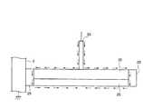
以下、添付図面を参照して本発明の実施の形態について説明する。図1は本発明の一実施形態に係るプラズマ処理装置を模式的に示す断面図である。このプラズマ処理装置1は、電極板が上下平行に対向し、一方にプラズマ形成用電源が接続された容量結合型平行平板エッチング装置として構成されている。
【0035】
このプラズマ処理装置1は、例えば表面がアルマイト処理(陽極酸化処理)されたアルミニウムからなる円筒形状に成形されたチャンバー2を有しており、このチャンバー2は接地されている。前記チャンバー2内の底部にはセラミックなどの絶縁板3を介して、被処理体、例えば半導体ウエハ(以下「ウエハ」という)Wを載置するための略円柱状のサセプタ支持台4が設けられており、さらにこのサセプタ支持台4の上には、下部電極を構成するサセプタ5が設けられている。このサセプタ5にはハイパスフィルター(HPF)6が接続されている。
【0036】
前記サセプタ支持台4の内部には、冷媒室7が設けられており、この冷媒室7には、例えば液体窒素などの冷媒が冷媒導入管8を介して導入されて循環し、その冷熱が前記サセプタ5を介して前記ウエハWに対して伝熱され、これによりウエハWの処理面が所望の温度に制御される。
【0037】
前記サセプタ5は、その上中央部が凸状の円板状に成形され、その上にウエハWと略同形の静電チャック11が設けられている。静電チャック11は、絶縁材の間に電極12が介在されており、電極12に接続された直流電源13から例えば1.5kVの直流電圧が印加されることにより、例えばクーロン力によってウエハWを静電吸着する。
【0038】
そして、前記絶縁板3、サセプタ支持台4、サセプタ5、さらには前記静電チャック11には、被処理体であるウエハWの裏面に、伝熱媒体、例えばHeガスなどを供給するためのガス通路14が形成されており、この伝熱媒体を介してサセプタ5の冷熱がウエハWに伝達されウエハWが所定の温度に維持されるようになっている。
【0039】
前記サセプタ5の上端周縁部には、静電チャック11上に載置されたウエハWを囲むように、環状のフォーカスリング15が配置されている。このフォーカスリング15はシリコンなどの導電性材料からなっており、これによりエッチングの均一性が向上される。
【0040】
前記サセプタ5の上方には、このサセプタ5と平行に対向して上部電極21が設けられている。この上部電極21は、絶縁材25を介して、チャンバー2の上部に支持されており、サセプタ5との対向面を構成し、多数の吐出孔24を有する電極板23と、この電極板23を支持し、導電性材料、例えば表面がアルマイト処理されたアルミニウムからなる水冷構造の電極支持体22とによって構成されている。この電極21の詳細な構成については後述する。なお、サセプタ5と上部電極21とは、例えば10〜60mm程度離間している。
【0041】
前記上部電極21における電極支持体22にはガス導入口26が設けられ、さらにこのガス導入口26には、ガス供給管27が接続されており、このガス供給管27には、バルブ28、およびマスフローコントローラ29を介して、処理ガス供給源30が接続されている。処理ガス供給源30から、プラズマ処理、例えばエッチングのための処理ガスが供給される。
【0042】
処理ガスとしては、従来用いられている種々のものを採用することができ、例えばフロロカーボンガス(CxFy)やハイドロフロロカーボンガス(CpHqFr)のようなハロゲン元素を含有するガスを好適に用いることができる。他にAr、He等の希ガスやN2を添加してもよい。
【0043】
前記チャンバー2の底部には排気管31が接続されており、この排気管31には排気装置35が接続されている。排気装置35はターボ分子ポンプなどの真空ポンプを備えており、これによりチャンバー2内を所定の減圧雰囲気、例えば1Pa以下の所定の圧力まで真空引き可能なように構成されている。また、チャンバー2の側壁にはゲートバルブ32が設けられており、このゲートバルブ32を開にした状態でウエハWが隣接するロードロック室(図示せず)との間で搬送されるようになっている。
【0044】
上部電極21には、整合器41を介して第1の高周波電源40が接続されており、その際の給電は上部電極21の上面中央部に接続された給電棒33により行われる。また、上部電極21にはローパスフィルター(LPF)42が接続されている。この第1の高周波電源40は、27〜150MHzの範囲の周波数を有しており、このように高い周波数を印加することによりチャンバー2内に好ましい解離状態でかつ高密度のプラズマを形成することができ、低圧条件下のプラズマ処理が可能となる。この例では、高周波電源40として60MHzのものを用いている。
【0045】
下部電極としてのサセプタ5には、第2の高周波電源50が接続されており、その給電線には整合器51が介在されている。この第2の高周波電源50は1〜4MHzの範囲の周波数を有しており、このような範囲の周波数を印加することにより、被処理体であるウエハWに対してダメージを与えることなく適切なイオン作用を与えることができる。この例では、第2の高周波電源50として2MHzのものを用いている。
【0046】
次に、上部電極21の構成について詳細に説明する。
上部電極21の電極板23は、通常、SiやSiC等の導電体または半導体で構成されており、高周波電源40から給電棒33を介して供給される高周波電流が高周波数化すると、表皮効果により電極の極表面にしか電力が供給されず、図2に示すように、電力は給電棒33の表面、電極支持体22の上面、電極支持体22の側面、電極板23の側面を通ってプラズマ接触面である電極板23の下面に達する。この場合に、給電棒33は上部電極21の中心に存在しているため、電極板23下面のエッジ部ではどこも電力が同じ位相であり、図3に示すように、電極板23のエッジ部から同位相で中心方向へ徐々に電力が供給されるため、電極板23の中心とエッジ部とで位相差d/λ(λは電極表面波の波長、dは電極の半径)が生じる。印加周波数が高くなると、電極板23下面の径方向のインダクタンス(LωjΩ)を無視できなくなり、上記位相差による干渉作用によって、電極板23下面の中央部分のインピーダンスが低くなるため、電極板23下面の中心部分の電界強度がエッジ部分の電界強度よりも高くなる。また、中心位置はプラズマと接しているため、RF等価回路的には開放端となっている。したがって、プラズマへ供給される電界分布が定在波的となり、プラズマ密度の不均一を生じる。
【0047】
このようなプラズマ密度の不均一を解消するために、第1の例では、図4に示すように、電極板23を、例えば50mΩ・cm程度の低抵抗の導電体または半導体からなる外側部分61と、誘電体からなる中央部分62とにより構成する。このように誘電体により中央部分62を構成することにより、その部分においてプラズマとの間の容量成分が付加されることとなる。ここで、インピーダンスZは
Z=Lω−(1/Cω)j (ただし、ω=2πf(f:周波数))
で表すことできるから、誘電体部材62の容量Cにより、インピーダンスZにおける径方向のインダクタンス成分(Lω)を容量成分(−1/Cω)で打ち消すことができる。したがって、電極板23下面中央部において位相によるインピーダンスZの大きさの変化をほとんどなくすことができ、電極板23下面中央部の電界強度が低下し、電極下面からプラズマへ印加される電界が均一になってプラズマ密度を均一にすることができる。
【0048】
なお、この際の誘電体からなる中央部分62の径は、電極21の直径が300mmφの場合には、10〜50mmφが好ましい。また、中央部分62を構成する誘電体62の誘電率は、Lωを打ち消すことができる大きさであればよく、例えば誘電率3程度のポリイミド系樹脂を適用することができる。さらに、外側部分61としては、従来から電極板材料として使用されているSi、SiC等の導体または半導体を用いることができる。
【0049】
次に、上部電極21の第2の例について説明する。
第2の例では、図5に示すように、電極板23を、例えば50mΩ・cm程度の低抵抗の導電体または半導体からなる外側部分63と、例えば1〜100Ω・cmの相対的に抵抗が高い高抵抗部材からなる中央部分64とにより構成する。このように高抵抗部材で中央部分64を構成することにより、その部分で電力が供給される部分の厚さ、いわゆるスキンデップスδが変化する。つまり、スキンデップスδは、
δ=(2/ωσμ)1/2(ただし、σ:導電率、μ:透磁率)
と表すことができ、抵抗が大きくなって導電率σが低下するとスキンデップスδが大きくなる。そして、高抵抗部材64のスキンデップスδがその厚さよりも大きくなると、図6に示すように高抵抗部材64において高周波電力がその裏面にも供給されることとなり、高周波電力が高抵抗部材64の裏面側から下面に達するまでの間にジュール熱となって放出されることとなる。これにより、電極板23下面中央部において電界強度が低下することとなる。したがって、電極板23の下面の電界強度が均一となり、結果として電極下面からプラズマへ印加される電界が均一になってプラズマ密度を均一にすることができる。
【0050】
なお、この際の高抵抗部材からなる中央部分64の直径は、電極21の直径が300mmφの場合に50〜220mmφであることが好ましい。中央部分64を構成する高抵抗部材は、ボロン等のドーパントの量を調整するだけで抵抗を調整することができることからSiで構成することが好ましい。また、外側部分63としては、従来から電極板材料として使用されているSi、SiC等の導体または半導体を用いることができるが、電極板23全体をSiで構成し、ドーパント、例えばボロンのドープ量を変化させることにより外側部分63および高抵抗部材64を形成することがより簡便である。
【0051】
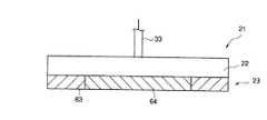
次に、上部電極21の第3の例について説明する。
この例では、図7に示すように、電極板23の裏面側中央に接するように誘電体部材65を設けている。ここでは電極板23として例えば1〜100Ω・cmの範囲の高抵抗の導電体または半導体を用い、スキンデップスδが電極板23の厚さよりも厚くなるようにする。これにより、高周波電力は電極板23の裏面側にも供給されるようになり、このように誘電体部材65を電極板23の裏面中央部に配置することにより、その部分においてプラズマとの間の容量成分が付加されることとなる。したがって、第1の例と同様、インピーダンスZにおける径方向のインダクタンス成分(Lω)を容量成分(−1/Cω)で打ち消すことができる。このため、電極板23下面中央部において位相によるインピーダンスZの大きさの変化が小さくなり、電極板23下面中央部の電界強度が低下し、電極下面からプラズマへ印加される電界が均一になってプラズマ密度を均一にすることができる。この例の場合には、第1および第2の例のように電極板23を2体化する必要がなく、従来と同様の一体的な導体または半導体からなる電極板を使用することができる。
【0052】
なお、この際の誘電体部材65の径は、電極21の直径が300mmφの場合には、50〜220mmφが好ましい。また、誘電体部材65の誘電率は、Lωを打ち消すことができる大きさであればよく、例えば誘電率3程度のポリイミド系樹脂を適用することができる。
【0053】
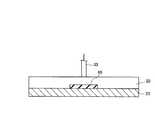
次に、上部電極21の第4の例について説明する。
この例では、図8に示すように、電極板23の裏面側中央に接するように高抵抗部材66を設けている。ここでは電極板23として例えば1〜100Ω・cmの範囲の高抵抗のものを用い、スキンデップスδが電極板23の厚さよりも厚くなるようにする。これにより、高周波電力は電極板23の裏面側にも供給されるようになり、このように高抵抗部材66を電極板23の裏面中央部に配置することにより、その部分に供給された高周波電力が高抵抗部材66においてジュール熱として放出され、これにより、電極板23下面中央部において電界強度が低下することとなる。したがって、電極板23の下面の電界強度が均一となり、結果として電極下面からプラズマへ印加される電界が均一になってプラズマ密度を均一にすることができる。この例の場合にも、第1および第2の例のように電極板23を2体化する必要がなく、従来と同様の一体的な導体または半導体からなる電極板を使用することができる。
【0054】
なお、この際の高抵抗部材66の直径は、電極21の直径が300mmφの場合に50〜220mmφであることが好ましい。高抵抗部材66はSiで構成することによりボロン等のドーパントの量を調整するだけで抵抗を調整することができるので好ましい。
【0055】
次に、上部電極21の第5の例について説明する。
この例では、図9に示すように、電極板23の下面に絶縁層67を形成している。この絶縁層67は、例えばセラミックスの溶射等により形成することができるが、その形成方法は問わない。このように絶縁層67を形成することにより、プラズマと電極板23とが絶縁層67を介して容量結合することとなる。したがって、RF等価回路的には、電極板23とプラズマとの間に多数のコンデンサーが並列に存在している状態となり、結果として電極板23下面の径方向のインダクタンス成分(Lω)を絶縁層67の容量成分(−1/Cω)で打ち消すことができる。したがって、電極板23下面において位相によるインピーダンスZの大きさの変化をほとんどなくすことができ、電極下面からプラズマへ印加される電界が均一になってプラズマ密度を均一にすることができる。
【0056】
なお、この際の絶縁層67は、インダクタンス成分(Lω)を打ち消すことができる程度の容量となるように、その材料および厚さが設定される。
【0057】
ところで、上部電極21の電極板23下面の電界分布が不均一になるのは、上述のような印加周波数を上昇させた際の電極表面のインダクタンスの径方向の変化に起因するばかりでなく、プラズマの非線形性の特性が顕著に現れ、プラズマからの反射波の高調波が増加し、このような高調波により電極表面に定在波が生成されることによっても生じる。
【0058】
つまり、プラズマからの反射波には多数の高調波が含まれており、これら高調波はさらに給電棒33のインダクタンス成分のため反射されるが、電極径が250〜300mmφとなると、高調波の中にはこれと定在波を形成する波長のものが含まれているため、電極板23の下面に定在波が形成されて電極板23表面中心部で電界強度が大きくなってしまう。
【0059】
そこで、上部電極21の第6の例では、図10に示すように、電極板23裏面側の中央部に接するように、例えばフェライト焼結体のような、電磁波吸収効果を有する部材68を設ける。このような電磁波吸収効果を有する部材68は高周波を吸収する機能を有するから、この部材68によりプラズマからの高調波を吸収する。これにより定在波が解消され、電極板23下面の電界分布が均一となり、プラズマ密度を均一にすることができる。この場合に、電磁波吸収効果を有する部材68としては、プラズマからの高調波は吸収するが、高周波電源40からの印加周波数は吸収しない特性を有するものを用いる。部材68の吸収周波数領域は、材料および組成によって調整することができる。
【0060】
以上の第1〜第6の例の上部電極は、印加周波数が27MHz以上で、プラズマ密度が1×10¹¹個/cm3以上の高密度の場合に特に有効である。
【0061】
次に、以上のような上部電極21を備えたプラズマ処理装置1における処理動作について、ウエハWに形成された酸化膜をエッチングする場合を例にとって説明する。
【0062】
まず、被処理体であるウエハWは、ゲートバルブ32が開放された後、図示しないロードロック室からチャンバー2内へと搬入され、静電チャック11上に載置される。そして、高圧直流電源13から直流電圧が印加されることによって、ウエハWが静電チャック11上に静電吸着される。次いで、ゲートバルブ32が閉じられ、排気機構35によって、チャンバー2内が所定の真空度まで真空引きされる。
【0063】
その後、バルブ28が開放されて、処理ガス供給源30から処理ガスがマスフローコントローラ29によってその流量が調整されつつ、処理ガス供給管27、ガス導入口26を通って上部電極21の内部へ導入され、さらに電極板23の吐出孔24を通って、図1の矢印に示すように、ウエハWに対して均一に吐出され、チャンバー2内の圧力が所定の値に維持される。
【0064】
そして、その後、第1の高周波電源40から27〜150MHz、例えば60MHzの高周波が上部電極21に印加される。これにより、上部電極21と下部電極としてのサセプタ5との間に高周波電界が生じ、処理ガスが解離してプラズマ化する。
【0065】
他方、第2の高周波電源50からは、1〜4MHz、例えば2MHzの高周波が下部電極であるサセプタ5に印加される。これにより、プラズマ中のイオンがサセプタ5側へ引き込まれ、イオンアシストによりエッチングの異方性が高められる。
【0066】
このように、上部電極21に印加する高周波の周波数を27MHzよりも高くすることにより、プラズマ密度を上げることができるが、従来の上部電極構造では、上述したように、印加周波数を上昇させた際の電極表面のインダクタンスの径方向の変化によって、または、プラズマからの反射波の高調波により電極板23下面に定在波が生成されることによって、電極板23下面での電界の不均一が生じる。これに対して、上部電極21を上記第1〜第6の例に示す構造にすることによって、これら電極板23下面での電界の不均一の原因のいずれかを解消することができるので、電極板23下面での電界分布を従来よりも均一にすることができ、プラズマ密度をより均一化することができる。すなわち、上記上部電極構造を採用することにより、印加する高周波の周波数が上昇し、プラズマ密度が上昇した際に生じる特有の問題を解消することができ、高密度でありながら均一なプラズマを形成することができる。したがって、エッチングの均一性が向上し、一層のデザインルールの微細化に適切に対応することが可能となる。特に、印加周波数が27MHz以上で、プラズマ密度が1×10¹¹個/cm3以上の場合に上記問題が生じやすく、以上のような上部電極構造はこのような場合に特に有効である。
【0067】
なお、本発明は上記実施の形態に限定されることなく、種々変形可能である。例えば、上記実施の形態では、上下電極に高周波を印加したが、上部電極のみに高周波を印加するタイプであってもよい。また、上部電極に27〜150MHzの高周波を印加した場合について示したが、この範囲に限るものではない。さらに、被処理基板として半導体ウエハを用い、これにエッチングを施す場合について説明したが、これに限らず、処理対象としては液晶表示装置(LCD)基板等の他の基板であってもよく、またプラズマ処理もエッチングに限らず、スパッタリング、CVD等の他の処理であってもよい。さらに、上記実施形態で示した上部電極の複数の例のいくつかを併用することも可能である。
【0068】
【発明の効果】
以上説明したように、本発明によれば、印加周波数を上昇させた際の電極板のプラズマ接触面のインダクタンスの径方向の変化による電界の不均一、または、プラズマからの反射波の高調波により電極板のプラズマ接触面に定在波が生成されることによって生じる電界の不均一を解消することができるので、電極板のプラズマ接触面での電界分布を従来よりも均一にすることができ、高密度プラズマにおけるプラズマ密度をより均一化することができる。
【図面の簡単な説明】
【図1】本発明の一実施形態に係るエッチング装置を示す断面図。
【図2】従来の上部電極における高周波電力の供給系路を模式的に示す断面図。
【図3】従来の上部電極における高周波電力の供給系路を模式的に示す底面図。
【図4】上部電極の第1の例を模式的に示す断面図。
【図5】上部電極の第2の例を模式的に示す断面図。
【図6】上部電極の第2の例の高周波電力の経路を模式的に示す図。
【図7】上部電極の第3の例を模式的に示す断面図。
【図8】上部電極の第4の例を模式的に示す断面図。
【図9】上部電極の第5の例を模式的に示す断面図。
【図10】上部電極の第6の例を模式的に示す断面図。
【符号の説明】
1;エッチング装置
2;チャンバー
5;サセプタ(第2の電極)
6;ハイパスフィルタ
21;上部電極(第1の電極)
23;電極板
30;処理ガス供給源
35;排気装置
40;第1の高周波電源
42;ローパスフィルタ
41,51;整合器
50;第2の高周波電源
61,63;外側部分
62;誘電体部材からなる中央部分
64;高抵抗部材からなる中央部分
65;誘電体部材
66;高抵抗部材
67;絶縁層
68;電磁波吸収効果を有する部材
W;半導体ウエハ[0001]
BACKGROUND OF THE INVENTION
The present invention relates to a plasma processing apparatus for performing plasma processing on a substrate such as a semiconductor substrate and an electrode used therefor.
[0002]
[Prior art]
For example, in a semiconductor device manufacturing process, plasma processing such as etching, sputtering, and CVD (chemical vapor deposition) is frequently used for a semiconductor wafer that is a substrate to be processed.
[0003]
Various plasma processing apparatuses for performing such plasma processing are used. Among them, a capacitively coupled parallel plate plasma processing apparatus is the mainstream.
[0004]
In the capacitively coupled parallel plate plasma processing apparatus, a pair of parallel plate electrodes (upper and lower electrodes) are arranged in a chamber, a processing gas is introduced into the chamber, and a high frequency is applied to at least one of the electrodes between the electrodes. A high-frequency electric field is formed on the semiconductor wafer, and a plasma of a processing gas is formed by the high-frequency electric field to perform plasma processing on the semiconductor wafer.
[0005]
When etching a film on a semiconductor wafer, such as an oxide film, with such a capacitively coupled parallel plate plasma processing apparatus, optimum radical control is possible by forming a medium density plasma with the chamber inside at an intermediate pressure. Thus, an appropriate plasma state can be obtained, and etching with high stability and reproducibility is realized with a high selection ratio.
[0006]
However, in recent years, design rules in USLI have been increasingly miniaturized, and a higher hole shape aspect ratio has been demanded. Conventional etching conditions are not necessarily sufficient.
[0007]
Thus, attempts have been made to form high-density plasma while increasing the frequency of the applied high-frequency power and maintaining a good plasma dissociation state. As a result, appropriate plasma can be formed under a lower pressure condition, and it is possible to appropriately cope with further miniaturization of design rules.
[0008]
[Problems to be solved by the invention]
By the way, according to the examination result of the present inventor, in such a plasma processing apparatus, since the upper electrode is a conductor or a semiconductor, it has been found that the following inconvenience occurs.
[0009]
As described above, when the applied frequency is increased in order to form a high-density plasma, the surface inductance of the electrode to which the high frequency is applied cannot be ignored, and the electric field distribution in the radial direction becomes nonuniform.
[0010]
In addition, when the plasma is densified in this way, the non-linear characteristic of the plasma appears remarkably, and the harmonics of the reflected wave from the plasma increase. When the electrode diameter becomes φ250 to φ300, a standing wave is generated on the electrode surface due to such harmonics, and the electric field distribution on the electrode surface is also nonuniform.
[0011]
If the electric field distribution becomes non-uniform in this way, the plasma density becomes non-uniform and the etching rate distribution becomes non-uniform. Therefore, the etching rate distribution can be made uniform by removing one of the causes of the non-uniform electric field distribution. Necessary.
[0012]
However, the problems in the case of using such high-density plasma have not been clearly recognized in the past, and no attempt has been made to eliminate the above-described uneven electric field distribution.
[0013]
The present invention has been made in view of such circumstances, and in plasma processing using high-density plasma that can cope with further miniaturization, a plasma processing apparatus capable of reducing non-uniformity of electric field distribution on the electrode surface And it aims at providing the electrode used therefor.
[0014]
[Means for Solving the Problems]
In order to solve the above problems, according to a first aspect of the present invention, in a state where a first electrode and a second electrode are provided in parallel in a chamber, and a substrate to be processed is supported by the second electrode. Then, while introducing the processing gas into the chamber held under reduced pressure, a high frequency electric field is formed between the first and second electrodes to generate plasma of the processing gas, and this plasma generates a predetermined plasma on the substrate to be processed. A plasma processing apparatus for performing processing,
The first electrode includes an electrode plate provided to face the second electrode. The electrode plate includes an outer portion made of a conductor or a semiconductor, and a dielectric portion.With woodHaving a central portion configured;The surface on the second electrode side of the electrode plate is formed so that the outer portion and the central portion are flat,A high-frequency power is applied to the first electrode from a surface opposite to the second electrode. A plasma processing apparatus is provided.
The diameter of the central portion made of the dielectric member is preferably 10 to 50 mm.
[0015]
According to a second aspect of the invention,The first and second electrodes are provided in parallel in the chamber, and the first gas is introduced into the chamber held under reduced pressure while the substrate to be processed is supported by the second electrode. A plasma processing apparatus for generating a plasma of a processing gas by forming a high-frequency electric field between the second electrode and the second electrode, and performing a predetermined plasma processing on the substrate to be processed by the plasma,
The first electrode includes an electrode plate provided to face the second electrode. The electrode plate includes an outer portion made of a conductor or a semiconductor and a central portion made of a high resistance member. And the second electrode side surface of the electrode plate is formed such that the outer portion and the central portion are flat, and the first electrode includes the second electrode and the second electrode. A plasma processing apparatus is formed in which high frequency power is applied from the opposite surface.
The diameter of the central portion made of the high resistance member is preferably 50 to 220 mm.
[0016]
In the first and second aspects, it is preferable that a skin depth δ represented by the following formula (1) of the central portion made of the high resistance member is larger than the thickness of the central portion of the electrode plate.
δ = (2 / ωσμ)1/2...... (1)
Where ω = 2πf (f: frequency), σ: conductivity, μ: permeability.
Also, the electrode plateSaidOuter part andSaidAll the central parts are made of Si, and the doping amount of the dopant is varied.SaidWith the outer partSaidIt is preferable to form a central portion.
[0017]
According to a third aspect of the present invention,The first and second electrodes are provided in parallel in the chamber, and the first gas is introduced into the chamber held under reduced pressure while the substrate to be processed is supported by the second electrode. A plasma processing apparatus for generating a plasma of a processing gas by forming a high-frequency electric field between the second electrode and the second electrode, and applying a predetermined plasma processing to the substrate to be processed by the plasma,
The first electrode includes an electrode plate made of a conductor or a semiconductor provided so as to face the second electrode, and a dielectric portionMaterialThe electrode plate is provided so as to be in contact with the central portion of the surface opposite to the second electrode side, and high frequency power is applied to the first electrode from the surface opposite to the second electrode. A plasma processing apparatus is provided.
[0018]
According to the fourth aspect of the present invention, the first and second electrodes are provided in parallel in the chamber, and the chamber held under reduced pressure in a state where the substrate to be processed is supported by the second electrode. A plasma processing apparatus for generating a plasma of a processing gas by forming a high-frequency electric field between the first and second electrodes while introducing a processing gas into the substrate, and performing a predetermined plasma processing on the substrate to be processed by the plasma. And
The first electrode includes an electrode plate made of a conductor or a semiconductor provided so as to face the second electrode, and the high resistance member is disposed on the opposite side of the electrode plate from the second electrode side. A plasma processing apparatus is provided, wherein the plasma processing apparatus is provided so as to be in contact with a central portion of a surface, and high-frequency power is applied to the first electrode from a surface opposite to the second electrode.
[0019]
In the third and fourth aspects, the electrode plate preferably has a skin depth δ represented by the following formula (1) larger than the thickness of the electrode plate.
δ = (2 / ωσμ)1/2...... (1)
Where ω = 2πf (f: frequency), σ: conductivity, μ: permeability.
The diameter of the dielectric member or the high resistance member is preferably 50 to 220 mm.
Furthermore, the resistance of the electrode plate is preferably 1 to 100 Ω · cm.
Furthermore, it is preferable that the whole of the dielectric member or the high resistance member is covered with the electrode plate and the electrode support.
Furthermore, it is preferable that a gas supply pipe is connected to the electrode support, and the processing gas is supplied through the electrode plate.
[0020]
Of the present inventionFifth viewpointAccording to the method, the first and second electrodes are provided in parallel in the chamber, and the processing gas is introduced into the chamber held under reduced pressure in a state where the substrate to be processed is supported by the second electrode. A plasma processing apparatus for forming a plasma of a processing gas by forming a high-frequency electric field between the first and second electrodes and applying a predetermined plasma processing to the substrate to be processed by the plasma,
The first electrode is provided so as to face the second electrode, and includes an electrode plate made of a conductor or a semiconductor, and a member having an electromagnetic wave absorption effect is opposite to the second electrode side of the electrode plate. A high frequency power is applied to the first electrode from the central portion of the surface opposite to the second electrode, the plasma processing apparatus being provided so as to be in contact with the central portion of the side surface Is provided.
[0021]
Each plasma aboveprocessingIn the apparatus, the frequency of the high-frequency power applied to the first electrode is 27 MHz or more, and the density of plasma formed is 1 × 10¹¹Piece / cm3The above is preferable.
[0022]
Of the present inventionSixth viewpointAccording to the method, the first and second electrodes are provided in parallel in the chamber, and the processing gas is introduced into the chamber held under reduced pressure in a state where the substrate to be processed is supported by the second electrode. An electrode used as a first electrode of a plasma processing apparatus for forming a plasma of a processing gas by forming a high-frequency electric field between the first and second electrodes and applying a predetermined plasma processing to the substrate to be processed by the plasma. Because
An electrode plate is provided so as to face the second electrode. The electrode plate includes an outer portion made of a conductor or a semiconductor, and a dielectric portion.With woodHaving a central portion configured;The surface on the second electrode side of the electrode plate is formed so that the outer portion and the central portion are flat,The electrode is provided with high-frequency power applied from a surface opposite to the second electrode.
The diameter of the central portion made of the dielectric member is preferably 10 to 50 mm.
[0023]
According to the seventh aspect of the present invention, a chamber that is held under reduced pressure in a state where first and second electrodes are provided in parallel in a chamber, and a substrate to be processed is supported by the second electrode. In the plasma processing apparatus, a high-frequency electric field is formed between the first and second electrodes while a processing gas is introduced into the processing gas to generate plasma of the processing gas, and a predetermined plasma processing is performed on the substrate to be processed by the plasma. An electrode used as one electrode,
An electrode plate provided so as to face the second electrode, the electrode plate having an outer portion made of a conductor or a semiconductor and a central portion made of a high-resistance member; The surface on the second electrode side is formed so that the outer portion and the central portion are flat, and high frequency power is applied to the electrode from the surface opposite to the second electrode. An electrode is provided.
The diameter of the central portion made of the high resistance member is preferably 50 to 220 mm.
[0024]
In the sixth and seventh aspects, the skin depth δ represented by the following formula (1) of the central portion made of the high resistance member is preferably larger than the thickness of the central portion of the electrode plate. .
δ = (2 / ωσμ)1/2...... (1)
Where ω = 2πf (f: frequency), σ: conductivity, μ: permeability.
Also, the electrode plateSaidOuter part andSaidAll the central parts are made of Si, and the doping amount of the dopant is varied.SaidWith the outer partSaidIt is preferable to form a central portion.
[0025]
Of the present inventionEighth viewpointAccording to the method, the first and second electrodes are provided in parallel in the chamber, and the processing gas is introduced into the chamber held under reduced pressure in a state where the substrate to be processed is supported by the second electrode. An electrode used as a first electrode of a plasma processing apparatus for forming a plasma of a processing gas by forming a high-frequency electric field between the first and second electrodes and applying a predetermined plasma processing to the substrate to be processed by the plasma. Because
A dielectric part comprising an electrode plate made of a conductor or a semiconductor provided to face the second electrodeMaterialThe electrode plate is provided so as to be in contact with the central portion of the surface on the opposite side to the surface on the second electrode side, and high frequency power is applied to the electrode from the surface on the opposite side to the second electrode. An electrode is provided.
[0026]
According to the ninth aspect of the present invention, the chamber is held under reduced pressure in a state where the first and second electrodes are provided in parallel in the chamber, and the substrate to be processed is supported by the second electrode. In the plasma processing apparatus, a high-frequency electric field is formed between the first and second electrodes while a processing gas is introduced into the processing gas to generate plasma of the processing gas, and a predetermined plasma processing is performed on the substrate to be processed by the plasma. An electrode used as one electrode,
An electrode plate made of a conductor or a semiconductor is provided so as to face the second electrode, and the high resistance member is provided at the center of the surface opposite to the surface on the second electrode side of the electrode plate. An electrode is provided, wherein the electrode is provided so as to be in contact with the electrode, and high-frequency power is applied to the electrode from a surface opposite to the second electrode..
[0027]
In the eighth and ninth aspects, the electrode plate preferably has a skin depth δ represented by the following formula (1) larger than the thickness of the electrode plate.
δ = (2 / ωσμ)1/2...... (1)
Where ω = 2πf (f: frequency), σ: conductivity, μ: permeability.
The diameter of the dielectric member or the high resistance member is preferably 50 to 220 mm.
Furthermore, the resistance of the electrode plate is preferably 1 to 100 Ω · cm.
Furthermore, it is preferable that the whole of the dielectric member or the high resistance member is covered with the electrode plate and the electrode support.
Furthermore, it is preferable that a gas supply pipe is connected to the electrode support, and the processing gas is supplied through the electrode plate.
[0028]
Of the present inventionTenth aspectAccording to the method, the first and second electrodes are provided in parallel in the chamber, and the processing gas is introduced into the chamber held under reduced pressure in a state where the substrate to be processed is supported by the second electrode. An electrode used as a first electrode in a plasma processing apparatus for forming a plasma of a processing gas by forming a high-frequency electric field between the first and second electrodes and applying a predetermined plasma processing to the substrate to be processed by the plasma. Because
An electrode plate made of a conductor or a semiconductor is provided so as to face the second electrode, and a member having an electromagnetic wave absorption effect is provided on a surface opposite to the surface on the second electrode side of the electrode plate. An electrode is provided which is provided so as to be in contact with a central portion, and to which high-frequency power is applied from a surface opposite to the second electrode.
[0029]
In each of the above electrodes, the frequency of the applied high frequency power is 27 MHz or more, and the plasma density is 1 × 10 5.11Piece / cm3It is preferable to be used as described above.
[0030]
Of the present inventionFirst, second, sixth and seventh viewpointsThe central portion of the first electrode isDielectric material or high resistance materialIn the case of a dielectric member, it is possible to cancel the inductance component in the radial direction of the surface of the electrode plate in contact with the plasma by the capacitance component, and almost no change in impedance due to the phase can be eliminated. Therefore, in the case of a high resistance member, more high frequency power is consumed as Joule heat there, so that the electric field strength at the center of the surface of the electrode plate in contact with the plasma can be reduced, and the surface of the electrode plate Since the electric field supplied from the plasma to the plasma becomes uniform, the plasma density can be made uniform.
[0031]
Of the present inventionThird, fourth, eighth and ninth viewpointsAccording to the present invention, the electrode plate is in contact with the central portion of the surface opposite to the second electrode side.Dielectric material or high resistance materialBy providing the high frequency power to the dielectric member or the high resistance member, in the case of the dielectric member, the capacitive component cancels out the radial inductance component of the surface of the electrode plate in contact with the plasma. In the case of a high-resistance member, more high-frequency power is consumed as Joule heat, so that both of them are in contact with the plasma of the electrode plate. The electric field intensity at the center of the surface can be reduced, and the electric field supplied to the plasma from the surface of the electrode plate can be made uniform, so that the plasma density can be made uniform. Further, there is no need to make two electrode plates, and an electrode plate made of an integral conductor or semiconductor similar to the conventional one can be used.
[0033]
Of the present invention5th viewpoint and 10th viewpointAccording to the above, the member having the electromagnetic wave absorption effect is provided so as to be in contact with the central portion of the surface opposite to the second electrode side of the electrode plate, and the member having the electromagnetic wave absorption effect absorbs the high frequency. Since it has a function, harmonics from plasma can be absorbed by the member having the electromagnetic wave absorption effect. As a result, the standing wave formed on the surface of the electrode plate in contact with the plasma is eliminated, the electric field distribution on the surface of the electrode plate in contact with the plasma becomes uniform, and the plasma density can be made uniform.
[0034]
DETAILED DESCRIPTION OF THE INVENTION
Hereinafter, embodiments of the present invention will be described with reference to the accompanying drawings. FIG. 1 is a cross-sectional view schematically showing a plasma processing apparatus according to an embodiment of the present invention. The plasma processing apparatus 1 is configured as a capacitively coupled parallel plate etching apparatus in which electrode plates are opposed in parallel in the vertical direction, and a plasma forming power source is connected to one of them.
[0035]
The plasma processing apparatus 1 has a
[0036]
A refrigerant chamber 7 is provided inside the susceptor support 4, and a refrigerant such as liquid nitrogen is introduced into the refrigerant chamber 7 through a
[0037]
The
[0038]
The insulating plate 3, the susceptor support 4, the
[0039]
An
[0040]
An
[0041]
A
[0042]
As the processing gas, various conventionally used gases can be employed. For example, fluorocarbon gas (CxFy) And hydrofluorocarbon gas (CpHqFrA gas containing a halogen element such as) can be suitably used. In addition, noble gases such as Ar and He and N2May be added.
[0043]
An
[0044]
A first high
[0045]
A second high
[0046]
Next, the configuration of the
The
[0047]
In order to eliminate such plasma density non-uniformity, in the first example, as shown in FIG. 4, the
Z = Lω− (1 / Cω) j (where ω = 2πf (f: frequency))
Therefore, due to the capacitance C of the
[0048]
In this case, the diameter of the
[0049]
Next, a second example of the
In the second example, as shown in FIG. 5, the
δ = (2 / ωσμ)1/2(However, σ: conductivity, μ: permeability)
When the resistance increases and the conductivity σ decreases, the skin depth δ increases. When the skin depth δ of the
[0050]
In this case, the diameter of the
[0051]
Next, a third example of the
In this example, as shown in FIG. 7, a
[0052]
In this case, the diameter of the
[0053]
Next, a fourth example of the
In this example, as shown in FIG. 8, a
[0054]
The diameter of the
[0055]
Next, a fifth example of the
In this example, as shown in FIG. 9, an insulating
[0056]
Note that the material and thickness of the insulating
[0057]
By the way, the electric field distribution on the lower surface of the
[0058]
In other words, the reflected wave from the plasma includes a large number of harmonics, and these harmonics are further reflected due to the inductance component of the
[0059]
Therefore, in the sixth example of the
[0060]
The upper electrodes of the above first to sixth examples have an applied frequency of 27 MHz or more and a plasma density of 1 × 10.11Piece / cm3This is particularly effective in the case of the above high density.
[0061]
Next, the processing operation in the plasma processing apparatus 1 including the
[0062]
First, after the
[0063]
Thereafter, the
[0064]
Then, a high frequency of 27 to 150 MHz, for example, 60 MHz is applied to the
[0065]
On the other hand, a high frequency of 1 to 4 MHz, for example, 2 MHz is applied from the second high
[0066]
As described above, the plasma density can be increased by setting the frequency of the high frequency applied to the
[0067]
The present invention is not limited to the above-described embodiment, and various modifications can be made. For example, in the above embodiment, a high frequency is applied to the upper and lower electrodes, but a type in which a high frequency is applied only to the upper electrode may be used. Moreover, although the case where the high frequency of 27-150 MHz was applied to the upper electrode was shown, it does not restrict to this range. Further, the case where a semiconductor wafer is used as a substrate to be processed and etching is performed has been described. The plasma processing is not limited to etching, and may be other processing such as sputtering and CVD. Furthermore, some of the plurality of examples of the upper electrode shown in the above embodiment can be used in combination.
[0068]
【The invention's effect】
As described above, according to the present invention, the electric field is uneven due to a change in the radial direction of the inductance of the plasma contact surface of the electrode plate when the applied frequency is increased, or due to harmonics of reflected waves from the plasma. Since it is possible to eliminate the non-uniformity of the electric field caused by the generation of standing waves on the plasma contact surface of the electrode plate, the electric field distribution on the plasma contact surface of the electrode plate can be made more uniform than before, The plasma density in the high-density plasma can be made more uniform.
[Brief description of the drawings]
FIG. 1 is a cross-sectional view showing an etching apparatus according to an embodiment of the present invention.
FIG. 2 is a cross-sectional view schematically showing a high-frequency power supply system in a conventional upper electrode.
FIG. 3 is a bottom view schematically showing a high-frequency power supply system in a conventional upper electrode.
FIG. 4 is a cross-sectional view schematically showing a first example of an upper electrode.
FIG. 5 is a cross-sectional view schematically showing a second example of the upper electrode.
FIG. 6 is a diagram schematically showing a path of high-frequency power in a second example of the upper electrode.
FIG. 7 is a cross-sectional view schematically showing a third example of the upper electrode.
FIG. 8 is a cross-sectional view schematically showing a fourth example of the upper electrode.
FIG. 9 is a cross-sectional view schematically showing a fifth example of the upper electrode.
FIG. 10 is a sectional view schematically showing a sixth example of the upper electrode.
[Explanation of symbols]
1: Etching equipment
2; chamber
5: Susceptor (second electrode)
6; High-pass filter
21: Upper electrode (first electrode)
23: Electrode plate
30; processing gas supply source
35; exhaust system
40; first high frequency power supply
42; low-pass filter
41, 51; matching device
50; second high-frequency power supply
61, 63; outer part
62; central portion made of a dielectric member
64; central portion made of a high resistance member
65; dielectric member
66; high resistance member
67; Insulating layer
68; Member having electromagnetic wave absorption effect
W: Semiconductor wafer
Claims (30)
Translated fromJapanese前記第1の電極は、第2の電極に対向するように設けられた電極板を備え、この電極板は、導電体または半導体で構成された外側部分と、誘電体部材で構成された中央部分とを有し、前記電極板の前記第2電極側の面は、前記外側部分と前記中央部分とが平らになるように形成され、前記第1の電極には、その前記第2の電極と反対側の面から高周波電力が印加されることを特徴とするプラズマ処理装置。The first and second electrodes are provided in parallel in the chamber, and the first gas is introduced into the chamber held under reduced pressure while the substrate to be processed is supported by the second electrode. A plasma processing apparatus for generating a plasma of a processing gas by forming a high-frequency electric field between the second electrode and the second electrode, and performing a predetermined plasma processing on the substrate to be processed by the plasma,
Said first electrode comprises an electrode plate provided so as to face the second electrode, the electrode plate, an outer portion made of a conductor or semiconductor, which isa dielectricmember center Andthe second electrode side surface of the electrode plate is formed such that the outer portion and the central portion are flat, and the first electrode includes the second electrode. A plasma processing apparatus, wherein high frequency power is applied from a surface opposite to the surface.
前記第1の電極は、第2の電極に対向するように設けられた電極板を備え、この電極板は、導電体または半導体で構成された外側部分と、高抵抗部材で構成された中央部分とを有し、前記電極板の前記第2電極側の面は、前記外側部分と前記中央部分とが平らになるように形成され、前記第1の電極には、その前記第2の電極と反対側の面から高周波電力が印加されることを特徴とするプラズマ処理装置。 The first electrode includes an electrode plate provided to face the second electrode. The electrode plate includes an outer portion made of a conductor or a semiconductor and a central portion made of a high resistance member. And the second electrode side surface of the electrode plate is formed such that the outer portion and the central portion are flat, and the first electrode includes the second electrode and the second electrode. A plasma processing apparatus, wherein high-frequency power is applied from the opposite surface.
δ=(2/ωσμ)1/2 ……(1)
ただし、ω=2πf(f:周波数)、σ:導電率、μ:透磁率Said high the following equation (1) Skin represented by Deppusu ofsaid central portion comprising a resistance member δ is, inclaim 3 or claim 4, wherein greater than the thickness ofsaid central portion ofsaid electrode plate The plasma processing apparatus as described.
δ = (2 / ωσμ)1/2 (1)
Where ω = 2πf (f: frequency), σ: conductivity, μ: permeability.
前記第1の電極は、第2の電極に対向するように設けられた、導電体または半導体で構成された電極板を備え、誘電体部材がこの電極板の第2の電極側と反対側の面の中央部に接するように設けられ、前記第1の電極には、その前記第2の電極と反対側の面から高周波電力が印加されることを特徴とするプラズマ処理装置。The first and second electrodes are provided in parallel in the chamber, and the first gas is introduced into the chamber held under reduced pressure while the substrate to be processed is supported by the second electrode. A plasma processing apparatus for generating a plasma of a processing gas by forming a high-frequency electric field between the second electrode and the second electrode, and performing a predetermined plasma processing on the substrate to be processed by the plasma,
The first electrode is provided so as to face the second electrode, composed of a conductor or semiconductor is provided with an electrode plate, the dielectricmember is opposite to the second electrode side of the electrode plate A high frequency power is applied to the first electrode from a surface opposite to the second electrode. The plasma processing apparatus is provided so as to be in contact with a central portion of the surface.
前記第1の電極は、第2の電極に対向するように設けられた、導電体または半導体で構成された電極板を備え、高抵抗部材がこの電極板の第2の電極側と反対側の面の中央部に接するように設けられ、前記第1の電極には、その前記第2の電極と反対側の面から高周波電力が印加されることを特徴とするプラズマ処理装置。 The first electrode includes an electrode plate made of a conductor or a semiconductor provided so as to face the second electrode, and the high resistance member is disposed on the opposite side of the electrode plate from the second electrode side. A plasma processing apparatus, which is provided so as to be in contact with a central portion of a surface, and high-frequency power is applied to the first electrode from a surface opposite to the second electrode.
δ=(2/ωσμ)1/2 ……(1)
ただし、ω=2πf(f:周波数)、σ:導電率、μ:透磁率The plasma processing apparatus according toclaim 7 or 8 , wherein the electrode plate has a skin depth δ represented by the following expression (1) larger than a thickness of the electrode plate.
δ = (2 / ωσμ)1/2 (1)
Where ω = 2πf (f: frequency), σ: conductivity, μ: permeability.
前記第1の電極は、第2の電極に対向するように設けられ、導電体または半導体で構成された電極板を備え、電磁波吸収効果を有する部材がこの電極板の第2の電極側と反対側の面の中央部に接するように設けられ、前記第1の電極には、その前記第2の電極と反対側の面の中央部から高周波電力が印加されることを特徴とするプラズマ処理装置。The first and second electrodes are provided in parallel in the chamber, and the first gas is introduced into the chamber held under reduced pressure while the substrate to be processed is supported by the second electrode. A plasma processing apparatus for generating a plasma of a processing gas by forming a high-frequency electric field between the second electrode and the second electrode, and performing a predetermined plasma processing on the substrate to be processed by the plasma,
The first electrode is provided so as to face the second electrode, and includes an electrode plate made of a conductor or a semiconductor, and a member having an electromagnetic wave absorption effect is opposite to the second electrode side of the electrode plate. A high frequency power is applied to the first electrode from the central portion of the surface opposite to the second electrode, the plasma processing apparatus being provided so as to be in contact with the central portion of the side surface .
第2の電極に対向するように設けられる電極板を備え、この電極板は、導電体または半導体で構成された外側部分と、誘電体部材で構成された中央部分とを有し、前記電極板の前記第2電極側の面は、前記外側部分と前記中央部分とが平らになるように形成され、該電極には、その前記第2の電極と反対側となる面から高周波電力が印加されることを特徴とする電極。The first and second electrodes are provided in parallel in the chamber, and the first gas is introduced into the chamber held under reduced pressure while the substrate to be processed is supported by the second electrode. An electrode used as a first electrode of a plasma processing apparatus for forming a plasma of a processing gas by forming a high-frequency electric field between the second electrode and the plasma, and subjecting the substrate to be processed to a predetermined plasma processing by the plasma,
An electrode plate provided so as to face the second electrode, the electrode plate has a configured outer portion of a conductor or semiconductor, and a configured central portionwith a dielectricmember,said electrode The surface on the second electrode side of the plate is formed so that the outer portion and the central portion are flat, and high frequency power is applied to the electrode from the surface opposite to the second electrode. An electrode characterized by being made.
第2の電極に対向するように設けられる電極板を備え、この電極板は、導電体または半導体で構成された外側部分と、高抵抗部材で構成された中央部分とを有し、前記電極板の前記第2電極側の面は、前記外側部分と前記中央部分とが平らになるように形成され、該電極には、その前記第2の電極と反対側となる面から高周波電力が印加されることを特徴とする電極。 An electrode plate provided so as to face the second electrode, the electrode plate having an outer portion made of a conductor or a semiconductor and a central portion made of a high-resistance member; The surface on the second electrode side is formed so that the outer portion and the central portion are flat, and high frequency power is applied to the electrode from the surface opposite to the second electrode. An electrode characterized by that.
δ=(2/ωσμ)1/2 ……(1)
ただし、ω=2πf(f:周波数)、σ:導電率、μ:透磁率According toclaim 18 or 19wherein the high following (1) Skin Deppusu of formula ofsaid central portion comprising a resistance member δ, wherein greater than the thickness of the center portion ofthe electrode plate Electrodes.
δ = (2 / ωσμ)1/2 (1)
Where ω = 2πf (f: frequency), σ: conductivity, μ: permeability.
第2の電極に対向するように設けられる、導電体または半導体で構成された電極板を備え、誘電体部材がこの電極板の第2の電極側となる面と反対側の面の中央部に接するように設けられ、該電極には、その前記第2の電極と反対側となる面から高周波電力が印加されることを特徴とする電極。The first and second electrodes are provided in parallel in the chamber, and the first gas is introduced into the chamber held under reduced pressure while the substrate to be processed is supported by the second electrode. An electrode used as a first electrode of a plasma processing apparatus for forming a plasma of a processing gas by forming a high-frequency electric field between the second electrode and the plasma, and subjecting the substrate to be processed to a predetermined plasma processing by the plasma,
The second is disposed so as to face the electrode comprises a conductor or semiconductor electrode plate made of a dielectricmember central portion of the surface of the second electrode side becomes a surface opposite to the electrode plate A high frequency power is applied to the electrode from a surface opposite to the second electrode, the electrode being provided in contact with the electrode.
第2の電極に対向するように設けられる、導電体または半導体で構成された電極板を備え、高抵抗部材がこの電極板の第2の電極側となる面と反対側の面の中央部に接するように設けられ、該電極には、その前記第2の電極と反対側となる面から高周波電力が印加されることを特徴とする電極。The first and second electrodes are provided in parallel in the chamber, and the first gas is introduced into the chamber held under reduced pressure while the substrate to be processed is supported by the second electrode. An electrode used as a first electrode of a plasma processing apparatus for forming a plasma of a processing gas by forming a high-frequency electric field between the second electrode and the plasma, and subjecting the substrate to be processed to a predetermined plasma processing by the plasma,
An electrode plate made of a conductor or a semiconductor is provided so as to face the second electrode, and the high resistance member is provided at the center of the surface opposite to the surface on the second electrode side of the electrode plate. An electrode, wherein the electrode is provided in contact with the electrode, and high-frequency power is applied to the electrode from a surface opposite to the second electrode .
δ=(2/ωσμ)1/2 ……(1)
ただし、ω=2πf(f:周波数)、σ:導電率、μ:透磁率The electrode according toclaim 22 or 23 , wherein the electrode plate has a skin depth δ represented by the following formula (1) larger than a thickness of the electrode plate.
δ = (2 / ωσμ)1/2 (1)
Where ω = 2πf (f: frequency), σ: conductivity, μ: permeability.
第2の電極に対向するように設けられる、導電体または半導体で構成された電極板を備え、電磁波吸収効果を有する部材がこの電極板の第2の電極側となる面と反対側の面の中央部に接するように設けられ、該電極には、その前記第2の電極と反対側となる面から高周波電力が印加されることを特徴とする電極。The first and second electrodes are provided in parallel in the chamber, and the first gas is introduced into the chamber held under reduced pressure while the substrate to be processed is supported by the second electrode. An electrode used as a first electrode in a plasma processing apparatus for forming a plasma of a processing gas by forming a high-frequency electric field between the second electrode and the plasma, and subjecting the substrate to be processed to a predetermined plasma processing by the plasma,
An electrode plate made of a conductor or a semiconductor is provided so as to face the second electrode, and a member having an electromagnetic wave absorption effect is provided on a surface opposite to the surface on the second electrode side of the electrode plate. An electrode, wherein the electrode is provided in contact with a central portion, and high-frequency power is applied to the electrode from a surface opposite to the second electrode.
Priority Applications (12)
| Application Number | Priority Date | Filing Date | Title |
|---|---|---|---|
| JP12687899AJP4454718B2 (en) | 1999-05-07 | 1999-05-07 | Plasma processing apparatus and electrodes used therefor |
| DE60043505TDE60043505D1 (en) | 1999-05-06 | 2000-04-27 | APPARATUS FOR PLASMA TREATMENT |
| KR20017014080AKR100880767B1 (en) | 1999-05-06 | 2000-04-27 | Plasma processing equipment |
| PCT/JP2000/002770WO2000068985A1 (en) | 1999-05-06 | 2000-04-27 | Apparatus for plasma processing |
| EP00922892AEP1193746B1 (en) | 1999-05-06 | 2000-04-27 | Apparatus for plasma processing |
| KR1020057007269AKR100748798B1 (en) | 1999-05-06 | 2000-04-27 | Plasma etching apparatus |
| US09/959,745US7537672B1 (en) | 1999-05-06 | 2000-04-27 | Apparatus for plasma processing |
| TW089108548ATW462092B (en) | 1999-05-06 | 2000-05-04 | Plasma processing system |
| US10/984,943US20050061445A1 (en) | 1999-05-06 | 2004-11-10 | Plasma processing apparatus |
| US12/195,842US8080126B2 (en) | 1999-05-06 | 2008-08-21 | Plasma processing apparatus |
| US12/879,926US20100326601A1 (en) | 1999-05-06 | 2010-09-10 | Plasma processing apparatus |
| US13/728,634US20130112666A1 (en) | 1999-05-06 | 2012-12-27 | Plasma processing apparatus |
Applications Claiming Priority (1)
| Application Number | Priority Date | Filing Date | Title |
|---|---|---|---|
| JP12687899AJP4454718B2 (en) | 1999-05-07 | 1999-05-07 | Plasma processing apparatus and electrodes used therefor |
Publications (3)
| Publication Number | Publication Date |
|---|---|
| JP2000323456A JP2000323456A (en) | 2000-11-24 |
| JP2000323456A5 JP2000323456A5 (en) | 2006-06-22 |
| JP4454718B2true JP4454718B2 (en) | 2010-04-21 |
Family
ID=14946093
Family Applications (1)
| Application Number | Title | Priority Date | Filing Date |
|---|---|---|---|
| JP12687899AExpired - LifetimeJP4454718B2 (en) | 1999-05-06 | 1999-05-07 | Plasma processing apparatus and electrodes used therefor |
Country Status (1)
| Country | Link |
|---|---|
| JP (1) | JP4454718B2 (en) |
Families Citing this family (35)
| Publication number | Priority date | Publication date | Assignee | Title |
|---|---|---|---|---|
| JP2003068718A (en)* | 2001-08-28 | 2003-03-07 | Hitachi Ltd | Plasma processing equipment |
| JP4047616B2 (en) | 2002-04-03 | 2008-02-13 | 東京エレクトロン株式会社 | Plasma processing apparatus and plasma processing method |
| JP4753276B2 (en) | 2002-11-26 | 2011-08-24 | 東京エレクトロン株式会社 | Plasma processing method and plasma processing apparatus |
| JP4584565B2 (en) | 2002-11-26 | 2010-11-24 | 東京エレクトロン株式会社 | Plasma processing apparatus and plasma processing method |
| JP4472372B2 (en) | 2003-02-03 | 2010-06-02 | 株式会社オクテック | Plasma processing apparatus and electrode plate for plasma processing apparatus |
| JP2005045067A (en)* | 2003-07-23 | 2005-02-17 | Matsushita Electric Ind Co Ltd | Semiconductor device manufacturing method and semiconductor device manufacturing apparatus |
| JP2005217240A (en) | 2004-01-30 | 2005-08-11 | Matsushita Electric Ind Co Ltd | Dry etching apparatus and dry etching method |
| US7767055B2 (en) | 2004-12-03 | 2010-08-03 | Tokyo Electron Limited | Capacitive coupling plasma processing apparatus |
| JP4642528B2 (en)* | 2005-03-31 | 2011-03-02 | 東京エレクトロン株式会社 | Plasma processing apparatus and plasma processing method |
| US7993489B2 (en)* | 2005-03-31 | 2011-08-09 | Tokyo Electron Limited | Capacitive coupling plasma processing apparatus and method for using the same |
| JP4615464B2 (en)* | 2006-03-16 | 2011-01-19 | 東京エレクトロン株式会社 | Electrode assembly for plasma processing apparatus and plasma processing apparatus |
| US8157953B2 (en) | 2006-03-29 | 2012-04-17 | Tokyo Electron Limited | Plasma processing apparatus |
| US20080006205A1 (en) | 2006-07-10 | 2008-01-10 | Douglas Keil | Apparatus and Method for Controlling Plasma Potential |
| JP5029089B2 (en)* | 2007-03-26 | 2012-09-19 | 東京エレクトロン株式会社 | Mounting table for plasma processing apparatus and plasma processing apparatus |
| JP5223377B2 (en) | 2008-02-29 | 2013-06-26 | 東京エレクトロン株式会社 | Electrode for plasma processing apparatus, plasma processing apparatus and plasma processing method |
| JP5204673B2 (en) | 2009-01-14 | 2013-06-05 | 東京エレクトロン株式会社 | Plasma processing apparatus and plasma distribution control method |
| JP5312369B2 (en)* | 2010-02-22 | 2013-10-09 | 東京エレクトロン株式会社 | Plasma processing apparatus and plasma processing method |
| JP5592129B2 (en) | 2010-03-16 | 2014-09-17 | 東京エレクトロン株式会社 | Plasma processing equipment |
| JP5674328B2 (en) | 2010-03-16 | 2015-02-25 | 東京エレクトロン株式会社 | Electrode and plasma processing apparatus |
| JP5982129B2 (en) | 2011-02-15 | 2016-08-31 | 東京エレクトロン株式会社 | Electrode and plasma processing apparatus |
| US9273393B2 (en) | 2014-01-25 | 2016-03-01 | Yuri Glukhoy | Torch system for depositing protective coatings on interior walls and recesses present on the flat surface of an object |
| KR101568722B1 (en)* | 2014-03-31 | 2015-11-12 | 최대규 | Plasma reactor and control method thereof |
| JP2022501833A (en)* | 2018-10-05 | 2022-01-06 | ラム リサーチ コーポレーションLam Research Corporation | Plasma processing chamber |
| JP7117734B2 (en) | 2018-12-06 | 2022-08-15 | 東京エレクトロン株式会社 | Plasma processing apparatus and plasma processing method |
| JP7162837B2 (en) | 2018-12-06 | 2022-10-31 | 東京エレクトロン株式会社 | Plasma processing apparatus and plasma processing method |
| KR102607686B1 (en) | 2018-12-06 | 2023-11-30 | 도쿄엘렉트론가부시키가이샤 | Shower plate, plasma processing device and plasma processing method |
| JP7408958B2 (en)* | 2019-09-05 | 2024-01-09 | Toto株式会社 | electrostatic chuck |
| JP7362030B2 (en)* | 2019-09-05 | 2023-10-17 | Toto株式会社 | electrostatic chuck |
| JP7301727B2 (en) | 2019-12-05 | 2023-07-03 | 東京エレクトロン株式会社 | Plasma processing apparatus and plasma processing method |
| JP7336378B2 (en) | 2019-12-16 | 2023-08-31 | 東京エレクトロン株式会社 | Plasma processing apparatus and plasma processing method |
| JP7360934B2 (en) | 2019-12-25 | 2023-10-13 | 東京エレクトロン株式会社 | Plasma processing equipment and plasma processing method |
| US11139147B1 (en) | 2020-05-26 | 2021-10-05 | Tokyo Electron Limited | Plasma processing apparatus |
| US20230207280A1 (en)* | 2021-12-29 | 2023-06-29 | Semes Co., Ltd. | Substrate treating apparatus |
| TW202429512A (en)* | 2022-09-09 | 2024-07-16 | 日商東京威力科創股份有限公司 | Electrode plate, electrode assembly, and plasma processing device |
| JP2024072409A (en)* | 2022-11-16 | 2024-05-28 | 東京エレクトロン株式会社 | Plasma Processing Equipment |
- 1999
- 1999-05-07JPJP12687899Apatent/JP4454718B2/ennot_activeExpired - Lifetime
Also Published As
| Publication number | Publication date |
|---|---|
| JP2000323456A (en) | 2000-11-24 |
Similar Documents
| Publication | Publication Date | Title |
|---|---|---|
| JP4454718B2 (en) | Plasma processing apparatus and electrodes used therefor | |
| KR100880767B1 (en) | Plasma processing equipment | |
| JP4454781B2 (en) | Plasma processing equipment | |
| JP4230029B2 (en) | Plasma processing apparatus and etching method | |
| JP4831853B2 (en) | Capacitively coupled parallel plate plasma etching apparatus and plasma etching method using the same | |
| US20130112666A1 (en) | Plasma processing apparatus | |
| JP4584565B2 (en) | Plasma processing apparatus and plasma processing method | |
| JP4482308B2 (en) | Plasma processing apparatus and plasma processing method | |
| TWI333229B (en) | ||
| TWI488236B (en) | Focusing ring and plasma processing device | |
| JP5223377B2 (en) | Electrode for plasma processing apparatus, plasma processing apparatus and plasma processing method | |
| JP4493756B2 (en) | Plasma processing apparatus and plasma processing method | |
| CN100517563C (en) | Plasma processing device and plasma processing method | |
| TW201731131A (en) | Method and apparatus for clamping and declamping substrates using electrostatic chucks | |
| TW200423249A (en) | A system and method for controlling plasma with an adjustable coupling to ground circuit | |
| JP4047616B2 (en) | Plasma processing apparatus and plasma processing method | |
| JP4467667B2 (en) | Plasma processing equipment | |
| JP4322350B2 (en) | Plasma processing equipment | |
| JPH07302786A (en) | Apparatus for plasma treatment | |
| EP1143497A1 (en) | Plasma etching apparatus | |
| JP3328625B2 (en) | Plasma processing method and plasma processing apparatus | |
| KR20240002758A (en) | Plasma processing apparatus and plasma processing method using the same |
Legal Events
| Date | Code | Title | Description |
|---|---|---|---|
| A521 | Written amendment | Free format text:JAPANESE INTERMEDIATE CODE: A523 Effective date:20060427 | |
| A621 | Written request for application examination | Free format text:JAPANESE INTERMEDIATE CODE: A621 Effective date:20060427 | |
| A131 | Notification of reasons for refusal | Free format text:JAPANESE INTERMEDIATE CODE: A131 Effective date:20090616 | |
| A521 | Written amendment | Free format text:JAPANESE INTERMEDIATE CODE: A523 Effective date:20090811 | |
| TRDD | Decision of grant or rejection written | ||
| A01 | Written decision to grant a patent or to grant a registration (utility model) | Free format text:JAPANESE INTERMEDIATE CODE: A01 Effective date:20100202 | |
| A01 | Written decision to grant a patent or to grant a registration (utility model) | Free format text:JAPANESE INTERMEDIATE CODE: A01 | |
| A61 | First payment of annual fees (during grant procedure) | Free format text:JAPANESE INTERMEDIATE CODE: A61 Effective date:20100203 | |
| FPAY | Renewal fee payment (event date is renewal date of database) | Free format text:PAYMENT UNTIL: 20130212 Year of fee payment:3 | |
| R150 | Certificate of patent or registration of utility model | Free format text:JAPANESE INTERMEDIATE CODE: R150 | |
| FPAY | Renewal fee payment (event date is renewal date of database) | Free format text:PAYMENT UNTIL: 20130212 Year of fee payment:3 | |
| FPAY | Renewal fee payment (event date is renewal date of database) | Free format text:PAYMENT UNTIL: 20160212 Year of fee payment:6 | |
| R250 | Receipt of annual fees | Free format text:JAPANESE INTERMEDIATE CODE: R250 | |
| R250 | Receipt of annual fees | Free format text:JAPANESE INTERMEDIATE CODE: R250 | |
| EXPY | Cancellation because of completion of term |