JP4450719B2 - Manufacturing method of semiconductor device - Google Patents
Manufacturing method of semiconductor deviceDownload PDFInfo
- Publication number
- JP4450719B2 JP4450719B2JP2004307673AJP2004307673AJP4450719B2JP 4450719 B2JP4450719 B2JP 4450719B2JP 2004307673 AJP2004307673 AJP 2004307673AJP 2004307673 AJP2004307673 AJP 2004307673AJP 4450719 B2JP4450719 B2JP 4450719B2
- Authority
- JP
- Japan
- Prior art keywords
- layer
- diamond
- region
- electrode
- electrode formation
- Prior art date
- Legal status (The legal status is an assumption and is not a legal conclusion. Google has not performed a legal analysis and makes no representation as to the accuracy of the status listed.)
- Expired - Fee Related
Links
- 239000004065semiconductorSubstances0.000titleclaimsdescription65
- 238000004519manufacturing processMethods0.000titleclaimsdescription43
- 229910003460diamondInorganic materials0.000claimsdescription165
- 239000010432diamondSubstances0.000claimsdescription165
- 238000000034methodMethods0.000claimsdescription29
- 230000015572biosynthetic processEffects0.000claimsdescription26
- 239000000758substrateSubstances0.000claimsdescription25
- 229910052751metalInorganic materials0.000claimsdescription20
- 239000002184metalSubstances0.000claimsdescription20
- 238000010884ion-beam techniqueMethods0.000claimsdescription19
- VYPSYNLAJGMNEJ-UHFFFAOYSA-NSilicium dioxideChemical compoundO=[Si]=OVYPSYNLAJGMNEJ-UHFFFAOYSA-N0.000claimsdescription10
- 239000003870refractory metalSubstances0.000claimsdescription10
- 229910052814silicon oxideInorganic materials0.000claimsdescription10
- 239000012535impuritySubstances0.000claimsdescription9
- 230000001681protective effectEffects0.000claimsdescription9
- 229910052581Si3N4Inorganic materials0.000claimsdescription8
- PMHQVHHXPFUNSP-UHFFFAOYSA-Mcopper(1+);methylsulfanylmethane;bromideChemical compoundBr[Cu].CSCPMHQVHHXPFUNSP-UHFFFAOYSA-M0.000claimsdescription8
- 229910000449hafnium oxideInorganic materials0.000claimsdescription8
- WIHZLLGSGQNAGK-UHFFFAOYSA-Nhafnium(4+);oxygen(2-)Chemical compound[O-2].[O-2].[Hf+4]WIHZLLGSGQNAGK-UHFFFAOYSA-N0.000claimsdescription8
- 239000000463materialSubstances0.000claimsdescription8
- TWNQGVIAIRXVLR-UHFFFAOYSA-Noxo(oxoalumanyloxy)alumaneChemical compoundO=[Al]O[Al]=OTWNQGVIAIRXVLR-UHFFFAOYSA-N0.000claimsdescription8
- RVTZCBVAJQQJTK-UHFFFAOYSA-Noxygen(2-);zirconium(4+)Chemical compound[O-2].[O-2].[Zr+4]RVTZCBVAJQQJTK-UHFFFAOYSA-N0.000claimsdescription8
- HQVNEWCFYHHQES-UHFFFAOYSA-Nsilicon nitrideChemical compoundN12[Si]34N5[Si]62N3[Si]51N64HQVNEWCFYHHQES-UHFFFAOYSA-N0.000claimsdescription8
- 229910001928zirconium oxideInorganic materials0.000claimsdescription8
- GWEVSGVZZGPLCZ-UHFFFAOYSA-NTitan oxideChemical compoundO=[Ti]=OGWEVSGVZZGPLCZ-UHFFFAOYSA-N0.000claimsdescription6
- 229910002113barium titanateInorganic materials0.000claimsdescription6
- JRPBQTZRNDNNOP-UHFFFAOYSA-Nbarium titanateChemical compound[Ba+2].[Ba+2].[O-][Ti]([O-])([O-])[O-]JRPBQTZRNDNNOP-UHFFFAOYSA-N0.000claimsdescription6
- BPUBBGLMJRNUCC-UHFFFAOYSA-Noxygen(2-);tantalum(5+)Chemical compound[O-2].[O-2].[O-2].[O-2].[O-2].[Ta+5].[Ta+5]BPUBBGLMJRNUCC-UHFFFAOYSA-N0.000claimsdescription6
- VEALVRVVWBQVSL-UHFFFAOYSA-Nstrontium titanateChemical compound[Sr+2].[O-][Ti]([O-])=OVEALVRVVWBQVSL-UHFFFAOYSA-N0.000claimsdescription6
- 229910001936tantalum oxideInorganic materials0.000claimsdescription6
- OGIDPMRJRNCKJF-UHFFFAOYSA-Ntitanium oxideInorganic materials[Ti]=OOGIDPMRJRNCKJF-UHFFFAOYSA-N0.000claimsdescription6
- ZVWKZXLXHLZXLS-UHFFFAOYSA-Nzirconium nitrideChemical compound[Zr]#NZVWKZXLXHLZXLS-UHFFFAOYSA-N0.000claimsdescription6
- 229910052454barium strontium titanateInorganic materials0.000claimsdescription4
- 150000004767nitridesChemical class0.000claimsdescription3
- 229910000510noble metalInorganic materials0.000claimsdescription3
- 239000010408filmSubstances0.000description33
- 230000008569processEffects0.000description19
- XUIMIQQOPSSXEZ-UHFFFAOYSA-NSiliconChemical compound[Si]XUIMIQQOPSSXEZ-UHFFFAOYSA-N0.000description11
- 239000010703siliconSubstances0.000description11
- 229910052710siliconInorganic materials0.000description11
- 238000000206photolithographyMethods0.000description10
- 239000007789gasSubstances0.000description9
- 230000003071parasitic effectEffects0.000description8
- 239000013078crystalSubstances0.000description5
- 238000007796conventional methodMethods0.000description4
- 239000012212insulatorSubstances0.000description4
- 150000002500ionsChemical class0.000description4
- BASFCYQUMIYNBI-UHFFFAOYSA-NplatinumChemical compound[Pt]BASFCYQUMIYNBI-UHFFFAOYSA-N0.000description4
- ZOXJGFHDIHLPTG-UHFFFAOYSA-NBoronChemical compound[B]ZOXJGFHDIHLPTG-UHFFFAOYSA-N0.000description3
- 229910052796boronInorganic materials0.000description3
- 239000000969carrierSubstances0.000description3
- 238000005516engineering processMethods0.000description3
- 238000005530etchingMethods0.000description3
- 230000005669field effectEffects0.000description3
- 239000011810insulating materialSubstances0.000description3
- 230000007246mechanismEffects0.000description3
- 239000007769metal materialSubstances0.000description3
- 238000004544sputter depositionMethods0.000description3
- WFKWXMTUELFFGS-UHFFFAOYSA-NtungstenChemical compound[W]WFKWXMTUELFFGS-UHFFFAOYSA-N0.000description3
- 229910052721tungstenInorganic materials0.000description3
- 239000010937tungstenSubstances0.000description3
- KRHYYFGTRYWZRS-UHFFFAOYSA-NFluoraneChemical compoundFKRHYYFGTRYWZRS-UHFFFAOYSA-N0.000description2
- RTAQQCXQSZGOHL-UHFFFAOYSA-NTitaniumChemical compound[Ti]RTAQQCXQSZGOHL-UHFFFAOYSA-N0.000description2
- 229910052782aluminiumInorganic materials0.000description2
- XAGFODPZIPBFFR-UHFFFAOYSA-NaluminiumChemical compound[Al]XAGFODPZIPBFFR-UHFFFAOYSA-N0.000description2
- 125000004429atomChemical group0.000description2
- 230000008859changeEffects0.000description2
- 238000010586diagramMethods0.000description2
- 238000000609electron-beam lithographyMethods0.000description2
- PCHJSUWPFVWCPO-UHFFFAOYSA-NgoldChemical compound[Au]PCHJSUWPFVWCPO-UHFFFAOYSA-N0.000description2
- 229910052737goldInorganic materials0.000description2
- 239000010931goldSubstances0.000description2
- 238000001459lithographyMethods0.000description2
- VNWKTOKETHGBQD-UHFFFAOYSA-NmethaneChemical compoundCVNWKTOKETHGBQD-UHFFFAOYSA-N0.000description2
- 238000005268plasma chemical vapour depositionMethods0.000description2
- 229910052697platinumInorganic materials0.000description2
- 239000002994raw materialSubstances0.000description2
- 238000001004secondary ion mass spectrometryMethods0.000description2
- 238000001894space-charge-limited current methodMethods0.000description2
- 239000010409thin filmSubstances0.000description2
- 229910052719titaniumInorganic materials0.000description2
- 239000010936titaniumSubstances0.000description2
- GYHNNYVSQQEPJS-UHFFFAOYSA-NGalliumChemical compound[Ga]GYHNNYVSQQEPJS-UHFFFAOYSA-N0.000description1
- ZOKXTWBITQBERF-UHFFFAOYSA-NMolybdenumChemical compound[Mo]ZOKXTWBITQBERF-UHFFFAOYSA-N0.000description1
- GRYLNZFGIOXLOG-UHFFFAOYSA-NNitric acidChemical compoundO[N+]([O-])=OGRYLNZFGIOXLOG-UHFFFAOYSA-N0.000description1
- 238000004458analytical methodMethods0.000description1
- 230000008901benefitEffects0.000description1
- 230000005540biological transmissionEffects0.000description1
- 125000004432carbon atomChemical groupC*0.000description1
- 230000015556catabolic processEffects0.000description1
- 229910010293ceramic materialInorganic materials0.000description1
- 238000005229chemical vapour depositionMethods0.000description1
- 238000011109contaminationMethods0.000description1
- 230000008094contradictory effectEffects0.000description1
- 238000005520cutting processMethods0.000description1
- 230000007423decreaseEffects0.000description1
- 230000007547defectEffects0.000description1
- 238000000151depositionMethods0.000description1
- ZOCHARZZJNPSEU-UHFFFAOYSA-NdiboronChemical compoundB#BZOCHARZZJNPSEU-UHFFFAOYSA-N0.000description1
- 230000005684electric fieldEffects0.000description1
- 238000010894electron beam technologyMethods0.000description1
- 230000001747exhibiting effectEffects0.000description1
- 230000004927fusionEffects0.000description1
- 229910052733galliumInorganic materials0.000description1
- 229910052739hydrogenInorganic materials0.000description1
- 239000001257hydrogenSubstances0.000description1
- 125000004435hydrogen atomChemical class[H]*0.000description1
- 230000001678irradiating effectEffects0.000description1
- 229910052743kryptonInorganic materials0.000description1
- DNNSSWSSYDEUBZ-UHFFFAOYSA-Nkrypton atomChemical compound[Kr]DNNSSWSSYDEUBZ-UHFFFAOYSA-N0.000description1
- 239000007788liquidSubstances0.000description1
- 230000008018meltingEffects0.000description1
- 238000002844meltingMethods0.000description1
- 229910052750molybdenumInorganic materials0.000description1
- 239000011733molybdenumSubstances0.000description1
- 229910017604nitric acidInorganic materials0.000description1
- 238000000059patterningMethods0.000description1
- 238000001020plasma etchingMethods0.000description1
- 230000004044responseEffects0.000description1
- 238000004904shorteningMethods0.000description1
- 238000009751slip formingMethods0.000description1
- 238000003786synthesis reactionMethods0.000description1
- 229910052715tantalumInorganic materials0.000description1
- GUVRBAGPIYLISA-UHFFFAOYSA-Ntantalum atomChemical compound[Ta]GUVRBAGPIYLISA-UHFFFAOYSA-N0.000description1
- 229910052724xenonInorganic materials0.000description1
- FHNFHKCVQCLJFQ-UHFFFAOYSA-Nxenon atomChemical compound[Xe]FHNFHKCVQCLJFQ-UHFFFAOYSA-N0.000description1
Images


Landscapes
- Electrodes Of Semiconductors (AREA)
- Thin Film Transistor (AREA)
Description
Translated fromJapanese本発明は、ダイヤモンド薄膜を使用した半導体素子の製造方法に関し、特に、電界効果トランジスタ、発光ダイオード及びセンサ等として使用可能な半導体素子の製造方法に関する。 The present invention relates to a method for manufacturing a semiconductor element using a diamond thin film, and more particularly to a method for manufacturing a semiconductor element that can be used as a field effect transistor, a light emitting diode, a sensor, and the like.
ダイヤモンドは、室温における熱伝導率が物質中で最も高く、バンドギャップが5.47eVと広く、また飽和電子及びホール移動度が高く、更に絶縁破壊電圧も高いが、誘電率及び誘電損失は低い等、電子デバイスに必要とされる特性が他の半導体材料に比べて圧倒的に優れている。このため、ダイヤモンドは、超高性能の耐環境電子デバイス、高出力デバイス及び高周波デバイス等への応用が期待されている。 Diamond has the highest thermal conductivity at room temperature, wide band gap of 5.47 eV, high saturation electron and hole mobility, high dielectric breakdown voltage, low dielectric constant and dielectric loss, etc. The characteristics required for electronic devices are overwhelmingly superior to other semiconductor materials. For this reason, diamond is expected to be applied to ultra-high performance environment-resistant electronic devices, high-power devices, high-frequency devices, and the like.
従来、ダイヤモンド薄膜を使用した半導体素子としては、ゲート電極と動作層であるチャネル層との間に絶縁体層を挿入した絶縁ゲート型電界効果トランジスタ(Metal Insulator Semiconductor Field Effect Transistor:MISFET)がある(例えば、特許文献1及び2参照。)。 Conventionally, as a semiconductor element using a diamond thin film, there is an insulated gate field effect transistor (MISFET) in which an insulator layer is inserted between a gate electrode and a channel layer as an operation layer ( For example, see
図4は特許文献1に記載のMISFETの構造を示す断面図であり、図5は特許文献2に記載のMISFETの構造を示す断面図である。図4に示すように、特許文献1に記載のMISFET100は、絶縁性ダイヤモンド単結晶基板101上に、ホウ素が高濃度でドープされ、ソース及びドレインとなる高ドープp型半導体ダイヤモンド層102a及び102bが形成されている。また、絶縁性ダイヤモンド単結晶基板101上における高ドープp型半導体ダイヤモンド層102aと高ドープp型半導体ダイヤモンド層102bとの間には、これら高ドープp型半導体ダイヤモンド層102a及び102bよりも低濃度でホウ素がドープされたチャネル層である低ドープp型半導体ダイヤモンド層103が形成されている。更に、高ドープp型半導体ダイヤモンド層102a及び102b上には、夫々ソース電極104及びドレイン電極105が形成されており、低ドープp型半導体ダイヤモンド層103上には、絶縁体層となるアンドープダイヤモンド層106を介して、ゲート電極107が形成されている。 4 is a cross-sectional view showing the structure of the MISFET described in
このMISFET100は、ゲート電位が印加されていないときにチャネル領域にドレイン電流が流れ、ゲート電極107にソース電位に対して正の電位を印加することにより、ドレイン電流が抑制されるノーマリーオン型の電界効果トランジスタ(Field Effect Transistor:FET)である。このようなノーマリーオン型のFETにおいて、僅かなゲート電位を印加するだけでドレイン電流を大きく変化させるため、即ち、ドレイン電流の変化量とゲート電位の変化量との比である相互コンダクタンスを大きくするためには、ゲート電圧の影響がチャネル層の深い領域まで及ぶようにして、キャリアの空乏領域を大きく広げることが有効である。具体的には、ソース及びドレイン間に形成されたチャネル層におけるドナー又はアクセプタとなる不純物の濃度を低くすると共に、厚さをゲート電位の影響が及ぶ範囲にまで薄くすればよい。 The
一方、ドレイン電流を大きくするためには、チャネル層の厚さを厚くすると共に、チャネル層の不純物の濃度を高くして、キャリア濃度を高くしなければならない。このように、これらの条件は相反しており、同時に満足することはできない。従って、図4に示すような構造のFETは、実用特性が得られない。また、特許文献1に記載のMISFET100を製造する場合、フォトリソグラフィ工程を繰り返し行うことにより半導体ダイヤモンド層、絶縁層、ソース電極、ドレイン電極及びゲート電極を形成するため、全行程に約50ステップ以上が必要である。 On the other hand, in order to increase the drain current, it is necessary to increase the carrier concentration by increasing the thickness of the channel layer and increasing the concentration of impurities in the channel layer. Thus, these conditions are contradictory and cannot be satisfied at the same time. Therefore, the FET having the structure shown in FIG. 4 cannot obtain practical characteristics. In addition, when manufacturing the
また、図5に示すように、特許文献2に記載のMISFET110は、シリコン基板111上にアンドープ・ダイヤモンドからなる下地層112が形成されており、この下地層112上にソース及びドレインとなるn型半導体ダイヤモンド層113a及び113bと、チャネル層であるp型半導体ダイヤモンド層114とが形成されている。また、n型半導体ダイヤモンド層113a及び113b上には、夫々ソース電極115及びドレイン電極116が形成されており、p型半導体ダイヤモンド層114上には、一部がダイヤモンドからなる絶縁体層117を介してゲート電極118が形成されている。この特許文献2に記載のMISFET110は、ダイヤモンド単結晶基板を使用せず、シリコン基板111上に下地層112を形成し、この下地層112上に各層を形成することにより、製造コストの低減を図ったものであり、前述の特許文献1に記載のMISFET100と同様に、ノーマリーオン型のFETである。 Further, as shown in FIG. 5, in the
しかしながら、現時点では低抵抗のn型ダイヤモンドは合成されていないため、特許文献2に記載のFETは実現することができない。また、このFETを製造するためには、前述の特許文献1に記載のFETと同様に、フォトリソグラフィを繰り返し行って、半導体ダイヤモンド層、絶縁層、ソース電極、ドレイン電極及びゲート電極を形成するため、全行程に約70ステップ以上が必要である。 However, since the low resistance n-type diamond has not been synthesized at present, the FET described in Patent Document 2 cannot be realized. Further, in order to manufacture this FET, in the same manner as the FET described in
更に、ダイヤモンドが本来持っている電子及びホールの高い移動度は、ダイヤモンド層中の不純物及び結晶欠陥を極力少なくすることによって初めて発現するものである。このため、特許文献1及び2に記載のMISFETのように、チャネル層となるダイヤモンド層をドーピングにより半導体化した場合、ドーピング原子がキャリア移動度を低下させるため、高周波応答性等に限界があり、高周波トランジスタ等として実用化することは不可能である。 Furthermore, the high mobility of electrons and holes inherent to diamond is not manifested until the impurities and crystal defects in the diamond layer are minimized. For this reason, as in the MISFET described in
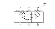
そこで、従来、チャネル層としてアンドープダイヤモンド層を使用することにより、高周波用トランジスタへの応用を可能にしたダイヤモンドFETが提案されている(特許文献3参照)。図6は特許文献3に記載のダイヤモンドFETの動作原理を示す模式図である。図6に示すように、特許文献3に記載のFET120においては、半導体ダイヤモンド層121と半導体ダイヤモンド層123との間に、比抵抗が100Ω・cm以上である高抵抗ダイヤモンド層122が設けられている。そして、半導体ダイヤモンド層121及び123上には、夫々ソース電極124及びドレイン電極126が形成されており、高抵抗ダイヤモンド層122上にはゲート電極125が形成されている。 Therefore, conventionally, a diamond FET has been proposed that can be applied to a high-frequency transistor by using an undoped diamond layer as a channel layer (see Patent Document 3). FIG. 6 is a schematic diagram showing the operation principle of the diamond FET described in
このダイヤモンドFET120においては、ソース電極124からドレイン電極126に到達するキャリアが、半導体ダイヤモンド層121、高抵抗ダイヤモンド層122及び半導体ダイヤモンド層123をこの順に流れる。そして、ゲート電極125に印加する電圧を変化させることにより、高抵抗ダイヤモンド層122のポテンシャルを変化させ、ソース電極124が接触する半導体ダイヤモンド層121から高抵抗ダイヤモンド層122へのキャリア注入量を制御している。このFET120は、前述のMISFETとは異なり、チャネル層に空乏層を拡げてドレイン電流を制御するものではないため、上述のような問題点はなく、実用的である。また、特許文献3に記載のFET120は、空間電荷制限電流(SCLC;Space-Charge-Limited Current)機構により電流が流れるため、特許文献1及び2に記載されているFETのように不純物伝達機構により電流が流れる場合よりも、ソース・ドレイン間に大きな電流を流すことができる。 In the
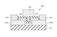
また、チャネル層として不純物濃度が低い低抵抗ダイヤモンド層を使用したFETも提案されている(特許文献4参照)。図7は特許文献4に記載のFETの構造を示す断面図である。図7に示すように、特許文献4に記載のFET130は、絶縁性ダイヤモンド基板131上に、ホウ素(B)が高濃度でドープされソース・ドレイン領域となる高ドープp型半導体ダイヤモンド層132a及び132bが局所的に形成されている。また、基板1並びに高ドープp型半導体ダイヤモンド層132a及び132bの一部を覆うように、Bが低濃度でソープされチャネル層となる低ドープp型半導体ダイヤモンド層135が形成されている。更に、高ドープp型半導体ダイヤモンド層132a及び132bには、夫々ソース電極133及びドレイン電極134が形成されており、低ドープp型半導体ダイヤモンド層135上には、酸化シリコン絶縁層136を介してゲート電極137が形成されている。 An FET using a low resistance diamond layer having a low impurity concentration as a channel layer has also been proposed (see Patent Document 4). FIG. 7 is a cross-sectional view showing the structure of the FET described in
このFET130は、チャネル層を低ドープp型半導体ダイヤモンド層136により形成しているため、チャネル層の結晶性が向上し、またキャリアをチャネル層に集中させることができるため、チャネル層をアンドープダイヤモンド層により形成した特許文献3に記載のFET120よりもFET特性を向上させることができる。 In this
しかしながら、前述の従来の技術には以下に示す問題点がある。即ち、特許文献4に記載のFET130は、特許文献1及び2に記載のMISFETと同様に、その製造工程において繰り返しフォトリソグラフィを行わなければならず、全行程に約70ステップ以上が必要であり、工程数が多いという問題点がある。また、特許文献3及び4に記載のFETにおいては、特性を向上させるためには、チャネル長、即ち、ソース領域とドレイン領域との距離を短くすると共に、ソース電極及びドレイン電極とゲート電極との間隔を短くして寄生抵抗及び寄生容量を低減する必要があるが、そのためには電子ビーム描画工程又はフォトリソグラフィ工程を繰り返し行わなければならず、工程数が増加するという問題点もある。 However, the conventional techniques described above have the following problems. That is, the FET 130 described in
本発明はかかる問題点に鑑みてなされたものであって、製造工程を簡素化することできると共に、工程数を増加させずに特性を向上させることができる半導体素子の製造方法を提供することを目的とする。 The present invention has been made in view of such problems, and it is possible to simplify the manufacturing process and provide a method for manufacturing a semiconductor element capable of improving characteristics without increasing the number of processes. Objective.
本発明に係る半導体素子の製造方法は、絶縁性ダイヤモンド基板上にその幅がソース領域及びドレイン領域間の距離と等しいギャップ層を形成する工程と、前記ギャップ層の両側にソース領域及びドレイン領域となる第1及び第2の導電性ダイヤモンド層を形成する工程と、前記ギャップ層を除去する工程と、前記基板上の前記第1及び第2の導電性ダイヤモンド層間の領域上に前記第1及び第2の導電性ダイヤモンド層に接触するように、前記第1及び第2の導電性ダイヤモンド層よりも電気抵抗が高くチャネル層となる高抵抗ダイヤモンド層を選択的に形成する工程と、前記高抵抗ダイヤモンド層上にゲート絶縁膜を選択的に形成する工程と、ゲート電極形成予定領域とソース電極形成予定領域との間及びゲート電極形成予定領域とドレイン電極形成予定領域との間に保護膜を形成する工程と、金属層を形成する工程と、前記金属層におけるソース電極形成予定領域、ドレイン電極形成予定領域及びゲート電極形成予定領域以外の部分を収束イオンビームにより除去する工程と、を有することを特徴とする。 The method of manufacturing a semiconductor device according to the present invention includes a step of forming a gap layer on the insulating diamond substrate having a width equal to the distance between the source region and the drain region, and a source region and a drain region on both sides of the gap layer. Forming the first and second conductive diamond layers, removing the gap layer, and forming the first and second conductive regions on the substrate between the first and second conductive diamond layers. A step of selectively forming a high-resistance diamond layer having a higher electrical resistance than the first and second conductive diamond layers so as to be a channel layer so as to be in contact with the two conductive diamond layers; A step of selectively forming a gate insulating film on the layer, a region between the gate electrode formation planned region and the source electrode formation planned region, and the gate electrode formation planned region and the drain Forming a protective film between the gate electrode formation scheduled region, a metal layer forming step, and a portion of the metal layer other than the source electrode formation planned region, the drain electrode formation planned region, and the gate electrode formation planned region. And removing with a focused ion beam.
本発明においては、絶縁性ダイヤモンド基板上にその幅がソース領域及びドレイン領域間の距離と等しいギャップ層を形成し、このギャップ層の両側にソース領域及びドレイン領域となる第1及び第2の導電性ダイヤモンド層を形成しているため、ソース領域とドレイン領域との距離、即ち、チャネル長を短くすることができる。これにより、工程数を増加させずに、寄生抵抗及び寄生容量を低減して、ダイヤモンド半導体素子の特性を向上させることができる。また、金属層を形成した後、収束イオンビームを使用して、この金属層におけるソース電極形成予定領域、ドレイン電極形成予定領域及びゲート電極形成予定領域以外の部分を除去することにより各電極を形成しているため、1回の処理でソース電極、ドレイン電極及びゲート電極の全てを形成することができる。その結果、リソグラフィ技術を利用して各電極を形成していた従来のダイヤモンド半導体素子の製造方法に比べて、製造工程を大幅に簡素化することができる。 In the present invention, a gap layer having a width equal to the distance between the source region and the drain region is formed on the insulating diamond substrate, and the first and second conductive layers serving as the source region and the drain region are formed on both sides of the gap layer. Since the conductive diamond layer is formed, the distance between the source region and the drain region, that is, the channel length can be shortened. Thereby, without increasing the number of steps, the parasitic resistance and the parasitic capacitance can be reduced and the characteristics of the diamond semiconductor element can be improved. In addition, after forming the metal layer, each electrode is formed by removing a portion other than the source electrode formation planned region, the drain electrode formation planned region and the gate electrode formation planned region in the metal layer using a focused ion beam. Therefore, all of the source electrode, the drain electrode, and the gate electrode can be formed by one treatment. As a result, the manufacturing process can be greatly simplified as compared with the conventional method of manufacturing a diamond semiconductor element in which each electrode is formed using lithography technology.
前記第1及び第2の導電性ダイヤモンド層は、例えば、高濃度でBがドープされた高ドープダイヤモンド層であり、前記高抵抗ダイヤモンド層は、例えば、前記第1及び第2の導電性ダイヤモンド層よりも低濃度でBがドープされた低ドープダイヤモンド層又は不純物をドープしていないアンドープダイヤモンド層である。これにより、ソース・ドレイン間に大電流を流すことができる。 The first and second conductive diamond layers are, for example, highly doped diamond layers doped with B at a high concentration, and the high resistance diamond layer is, for example, the first and second conductive diamond layers. It is a lightly doped diamond layer doped with B at a lower concentration or an undoped diamond layer not doped with impurities. As a result, a large current can flow between the source and the drain.
前記ギャップ層は、高融点金属、高融点金属の窒化物、高融点金属の炭化物、貴金属、酸化シリコン、酸化アルミニウム、酸化チタン、酸化タンタル、酸化ジルコニウム、酸化ハフニウム、窒化シリコン、窒化アルミニウム、窒化ジルコニウム、チタン酸バリウム及びチタン酸ストロンチウムからなる群から選択された少なくとも1種の材料により形成することができる。これにより、導電性ダイヤモンド層を形成する際のギャップ層の劣化を防止すると共に、導電性ダイヤモンド層形成後に容易に除去することができる。 The gap layer includes a refractory metal, a refractory metal nitride, a refractory metal carbide, a noble metal, silicon oxide, aluminum oxide, titanium oxide, tantalum oxide, zirconium oxide, hafnium oxide, silicon nitride, aluminum nitride, zirconium nitride. And at least one material selected from the group consisting of barium titanate and strontium titanate. This prevents the gap layer from being deteriorated when the conductive diamond layer is formed, and can be easily removed after forming the conductive diamond layer.
本発明によれば、収束イオンビームを使用して電極を形成することにより、マスク等のパターニング工程を行わずに、1ステップで複数の電極を形成することができるため、製造工程を大幅に簡素化することができると共に、素子構造を微細化することができるため、製造工程を増加させずに半導体素子の特性を向上させることができる。 According to the present invention, by forming an electrode using a focused ion beam, a plurality of electrodes can be formed in one step without performing a patterning process such as a mask, thereby greatly simplifying the manufacturing process. Since the device structure can be miniaturized, the characteristics of the semiconductor device can be improved without increasing the number of manufacturing steps.
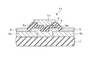
以下、本発明の実施の形態に係る半導体素子の製造方法について、添付の図面を参照して具体的に説明する。本実施形態においては、典型的なワイドバンドギャップ半導体であるダイヤモンドを使用し、最も高度な微細加工技術を必要とするダイヤモンドFETの製造方法を例にして説明する。図1は本実施形態のFETの構造を示す断面図である。図1に示すように、本実施形態のダイヤモンドFET11は、電気的に絶縁性であるダイヤモンド基板1上に、Bが高濃度でドープされソース領域及びドレイン領域となる導電性ダイヤモンド層3a及び3bが局所的に形成されている。このFET11における絶縁性ダイヤモンド基板1としては、例えば、ダイヤモンドの単結晶、ヘテロエピタキシャル膜、融合膜、高配向膜又は粒径の大きい多結晶膜等を使用することができる。また、ダイヤモンド膜を使用する場合の形態は、自立膜及びシリコン等の非ダイヤモンド基板上に形成されたもののいずれでもよい。 Hereinafter, a method for manufacturing a semiconductor device according to an embodiment of the present invention will be specifically described with reference to the accompanying drawings. In the present embodiment, a diamond FET manufacturing method that uses diamond, which is a typical wide band gap semiconductor, and that requires the most advanced fine processing technology will be described as an example. FIG. 1 is a cross-sectional view showing the structure of the FET of this embodiment. As shown in FIG. 1, in the
また、絶縁性ダイヤモンド基板1並びに導電性ダイヤモンド層3a及び3bの一部を覆うように、アンドープダイヤモンド層又は極微量のBがドープされたダイヤモンド層からなる高抵抗ダイヤモンド層4が形成されている。更に、導電性ダイヤモンド層3a及び3b上には、夫々ソース電極8及びドレイン電極9が形成されている。これらのソース電極8及びドレイン電極9は、金、白金、アルミニウム、チタン及びタングステン等の金属材料により形成されている。 Further, a high-
一方、高抵抗ダイヤモンド層4上にはゲート絶縁膜5が形成されている。このゲート絶縁膜5は、酸化シリコン、酸化アルミニウム、窒化シリコン、窒化アルミニウム、酸化ハフニウム、酸化ジルコニウムからなる群から選択された少なくとも1種の材料により形成されている。また、導電性ダイヤモンド層3a及び3bの表面におけるソース電極8及びドレイン電極9と高抵抗ダイヤモンド層4との間の領域、高抵抗ダイヤモンド層4及びゲート絶縁膜5の一部を覆うように、保護膜6a及び6bが形成されている。この保護膜6a及び6bは、電気的に絶縁性であり、導電性ダイヤモンド層3a及び3b、高抵抗ダイヤモンド層4及びゲート絶縁膜5との密着性が優れた材料により形成されていることが好ましく、例えば、酸化シリコン、酸化アルミニウム、酸化チタン、酸化タンタル、酸化ジルコニウム、酸化ハフニウム、窒化シリコン、窒化アルミニウム、窒化ジルコニウム、チタン酸バリウム及びチタン酸ストロンチウムからなる群から選択された少なくとも1種の絶縁材料により形成することができる。そして、ゲート絶縁膜5上、並びに保護膜6a及び6bにおけるゲート絶縁膜5上に形成されている部分の上には、ゲート電極10が形成されている。このゲート電極10は、ソース電極8及びドレイン電極9と同じ材料により形成されている。 On the other hand, a
本実施形態のダイヤモンドFET11においては、導電性ダイヤモンド層3a及び3bが夫々ソース領域及びドレイン領域となり、高抵抗ダイヤモンド層4における導電性ダイヤモンド層3a及び3b間の領域にチャネル領域が形成される。 In the
次に、このダイヤモンドFET11の製造方法について説明する。図2(a)乃至(d)及び図3(a)乃至(d)は本実施形態のFETの製造方法をその工程順に示す断面図である。先ず、図2(a)に示すダイヤモンド基板1を用意し、図2(b)に示すように、このダイヤモンド基板1上のソース・ドレイン間の領域、即ち、導電性ダイヤモンド層3aが形成される領域と導電性ダイヤモンド層3bが形成される領域との間に、通常の微細加工技術によりギャップ層2を形成する。 Next, a method for manufacturing the
ギャップ層2は、精確な形状加工が可能で、導電性ダイヤモンド層を蒸着する工程において劣化せず、更に導電性ダイヤモンド層形成後に除去することが可能な材料により形成されていることが好ましく、例えば、高融点金属、高融点金属の窒化物、高融点金属の炭化物、貴金属、酸化シリコン、酸化アルミニウム、酸化チタン、酸化タンタル、酸化ジルコニウム、酸化ハフニウム、窒化シリコン、窒化アルミニウム、窒化ジルコニウム、チタン酸バリウム及びチタン酸ストロンチウムからなる群から選択された少なくとも1種の材料により形成することができる。前述の高融点金属としては、タングステン、タンタル及びモリブデン等が挙げられるが、本発明はこれに限定されるものではなく、一般的なダイヤモンド合成温度(800℃程度)よりも融点が高い金属材料であればよい。また、ギャップ層2の幅は、ソース・ドレイン間の距離、即ち、チャネル長であり、適宜設定することができるが、ギャップ層2の幅が狭い程FETの特性は向上する。具体的には、ギャップ層2の幅は、1μm以下であることが好ましい。ギャップ層2の幅が1μmよりも広いと、ソース・ドレイン間の電気抵抗が大きくなり、実用的な特性が得られない。なお、本実施形態のFETの製造方法においては、ギャップ層2の幅を50nm以下にすることもできる。 The gap layer 2 is preferably formed of a material that can be precisely shaped, does not deteriorate in the process of depositing the conductive diamond layer, and can be removed after forming the conductive diamond layer. , Refractory metal, refractory metal nitride, refractory metal carbide, noble metal, silicon oxide, aluminum oxide, titanium oxide, tantalum oxide, zirconium oxide, hafnium oxide, silicon nitride, aluminum nitride, zirconium nitride, barium titanate And at least one material selected from the group consisting of strontium titanate. Examples of the refractory metal include tungsten, tantalum, and molybdenum. However, the present invention is not limited to this, and a metal material having a melting point higher than a general diamond synthesis temperature (about 800 ° C.). I just need it. The width of the gap layer 2 is the distance between the source and drain, that is, the channel length, and can be set as appropriate. The narrower the gap layer 2, the better the FET characteristics. Specifically, the width of the gap layer 2 is preferably 1 μm or less. If the width of the gap layer 2 is wider than 1 μm, the electrical resistance between the source and the drain increases, and practical characteristics cannot be obtained. In the FET manufacturing method of the present embodiment, the width of the gap layer 2 can be 50 nm or less.
次に、図2(c)に示すように、基板1上に、マイクロ波プラズマCVD(Chemical Vapor Deposition:化学気相成長)法により、厚さが例えば0.1μmであり、高濃度にBをドープした導電性ダイヤモンド層3a及び3bを形成する。その際、原料ガスとしては、例えばメタン(CH4)が0.3体積%、水素(H2)が99.7体積%である混合ガス中に、ドーピングガスとしてジボラン(B2H6)ガスを添加したものを使用し、原料ガス中のB及びCの原子比(B/C)を、例えば5000ppmとする。これにより、ドーピング濃度が、半導体・金属転位濃度(Bの場合は2×1020/cm−3)以上となるため、金属的な電気伝導性を示すダイヤモンド膜を合成することができる。また、成膜時のガス圧力は例えば6650Pa、基板温度は例えば800℃とする。これにより、図2(d)に示すように、基板1表面のギャップ層2が形成されていない領域上に、選択的に導電性ダイヤモンド層3a及び3bが形成される。なお、ギャップ層2上にはダイヤモンド膜は形成されにくいが、ギャップ層2上にダイヤモンド膜が形成された場合でも、導電性ダイヤモンド層3a及び3bと繋がっていなければ、後工程においてギャップ層2と共に除去されるため、問題はない。Next, as shown in FIG. 2C, the thickness of the
その後、図2(d)に示すように、例えばフッ酸及び硝酸等により、ギャップ層2を溶解除去する。このとき、導電性ダイヤモンド層3a及び3bの厚さがギャップ層2の厚さよりも薄いと、容易にギャップ層2を除去することができる。なお、図2(c)に示すように、導電性ダイヤモンド層3a及び3bの厚さがギャプ層2の厚さと同等であっても、ギャップ層2を除去する際に問題は生じない。但し、導電性ダイヤモンド層3a及び3bの厚さがギャップ層2の厚さよりも厚いとギャップ層2を除去し難くなる。特に、導電性ダイヤモンド層3a及び3bがギャップ層2を覆うように連続して形成されていると、その部分のギャップ層2は除去することができない。 Thereafter, as shown in FIG. 2D, the gap layer 2 is dissolved and removed, for example, with hydrofluoric acid and nitric acid. At this time, if the conductive diamond layers 3a and 3b are thinner than the gap layer 2, the gap layer 2 can be easily removed. As shown in FIG. 2C, even if the thickness of the conductive diamond layers 3a and 3b is equal to the thickness of the gap layer 2, no problem occurs when the gap layer 2 is removed. However, if the thickness of the conductive diamond layers 3a and 3b is larger than the thickness of the gap layer 2, it is difficult to remove the gap layer 2. In particular, when the conductive diamond layers 3a and 3b are continuously formed so as to cover the gap layer 2, the gap layer 2 in that portion cannot be removed.
次に、図3(a)に示すように、マイクロ波プラズマCVD法により、基板1表面における導電性ダイヤモンド層3aと導電性ダイヤモンド層3bとの間の領域、及び導電性ダイヤモンド層3a及び3bの一部を覆うように、不純物をドープせずに、又は、Bを極低濃度にドープして、チャネル層となる高抵抗ダイヤモンド層4を選択的に形成する。この高抵抗ダイヤモンド層4の厚さは、導電性ダイヤモンド層3a及び3bと同等又は導電性ダイヤモンド層3a及び3bよりもやや厚い程度であることが好ましく、例えば0.1μmである。また、高抵抗ダイヤモンド層4として、極低濃度にBをドープしたダイヤモンド層を形成する場合は、原料ガス中のB及びCの原子比(B/C)を、例えば0.5ppm未満にする。原料ガス中のB及びCの原子比(B/C)を0.5ppm以上にすると、ソース・ドレイン間の電流が不純物導電機構により流れるようになるため、FETにした際に大きな電流値が得られなくなる。なお、高抵抗ダイヤモンド層4は、導電性ダイヤモンド層3aと導電性ダイヤモンド層3bとの間及びその周辺部分に形成されていてばよく、厚さ以外には高精度の形状制御は不要である。 Next, as shown in FIG. 3A, the region between the conductive diamond layer 3a and the
次に、図3(b)に示すように、高抵抗ダイヤモンド層4上に、電子ビームリソグラフィ又はフォトリソグラフィを利用して、酸化シリコン、酸化アルミニウム、窒化シリコン、窒化アルミニウム、酸化ハフニウム、酸化ジルコニウムからなる群から選択された少なくとも1種の絶縁材料からなり、厚さが例えば0.05乃至1.00μmと極めて薄いゲート絶縁膜5を形成する。なお、ゲート絶縁膜5は、少なくともソース・ドレイン間に形成されるチャネル領域上に形成されていればよく、厚さ以外には高精度の形状制御は不要である。 Next, as shown in FIG. 3 (b), on the high
その後、図3(c)に示すように、前述のゲート絶縁膜5と同様に電子ビームリソグラフィ又はフォトリソグラフィを利用して、導電性ダイヤモンド層3a及び3bの一部、高抵抗ダイヤモンド層4及びゲート絶縁膜5の一部を覆うように、即ち、ゲート電極形成予定領域とソース電極形成予定領域との間及びゲート電極形成予定領域とドレイン電極形成予定領域との間に、酸化シリコン、酸化アルミニウム、酸化チタン、酸化タンタル、酸化ジルコニウム、酸化ハフニウム、窒化シリコン、窒化アルミニウム、窒化ジルコニウム、チタン酸バリウム及びチタン酸ストロンチウムからなる群から選択された少なくとも1種の絶縁材料からなり、厚さが例えば0.05乃至1.00μmである保護膜6a及び6bを形成する。この保護膜6a及び6bは、電極を形成する際に高抵抗ダイヤモンド層4及びゲート絶縁膜5を保護するものである。 Thereafter, as shown in FIG. 3C, using the electron beam lithography or photolithography similarly to the
次に、全体を覆うように、厚さが例えば0.05乃至1.00μmであり、金、白金、アルミニウム、チタン及びタングステン等の金属材料からなる電極金属層7を形成する。 Next, an electrode metal layer 7 having a thickness of, for example, 0.05 to 1.00 μm and made of a metal material such as gold, platinum, aluminum, titanium, and tungsten is formed so as to cover the whole.
そして、金属電極層7におけるソース電極8、ドレイン電極9及びゲート電極10となる部分以外の部分を収束イオンビームにより除去し、図1に示すダイヤモンドFETとする。収束イオンビーム(FIB:Forcused Ion Beam)装置は、電界で収束加速された液体ガリウム(Ga)イオン等を対象物に照射することにより対象物をエッチング加工する装置である。この収束イオンビーム装置は、ビーム径を絞ることによりサブミクロンオーダーの微細加工が可能、試料の二次電子像を見ることができるため加工領域の設定が容易等の特徴があり、従来、透過型電子顕微鏡(TEM:Transmission electron microscope)観察用試料の作製等に使用されている。しかしながら、収束イオンビーム加工は、加工速度が遅く、フォトリソグラフィにより一括露光する方が加工時間が短くなるため、シリコン等を使用した従来の半導体素子の製造工程においては、配線の切断加工等にしか使用されていないのが現状である。また、収束イオンビームを使用すると、Gaイオンによりシリコン半導体素子の表面が汚染されるため、シリコン半導体素子の製造工程には適用することができないという問題もある。一方、ダイヤモンド半導体素子は、シリコン半導体素子よりも特性が優れているため付加価値が高く、製造工程の一部に収束イオンビームを使用した加工速度が遅いステップが入っても問題はない。また、ダイヤモンド半導体素子は、シリコン半導体素子とは異なり、Gaイオンにより表面が汚染されても、洗浄すればよく、シリコン半導体素子のようにGaイオンが内部に入ってくることもない。更に、汚染を防止するため、Gaの代わりにキセノン(Xe)及びクリプトン(Kr)等のガスを使用することも可能である。 Then, portions other than the portions that become the
また、収束イオンビーム装置では、二次イオン質量分析が可能であり、加工部分の成分分析を行うことができる。そこで、本実施形態のFETの製造方法においては、金属電極層7をエッチングしている間は二次イオン質量分析を行い、下層の保護膜6a及び6bの成分原子、又は導電性ダイヤモンド層3a及び3bの炭素原子が検出され始めた時点で処理を完了する。これにより、下層にダメージを与えることなく、金属電極層7における電極形成予定領域以外の部分を除去することができる。 In addition, the focused ion beam apparatus can perform secondary ion mass spectrometry, and can perform component analysis of a processed portion. Therefore, in the FET manufacturing method of the present embodiment, secondary ion mass spectrometry is performed while the metal electrode layer 7 is being etched, and the component atoms of the lower
従来のFETの製造方法では、ソース電極及びドレイン電極とゲート電極とは、フォトリソグラフィ技術を利用して夫々別の工程で形成しているため、製造工程におけるステップ数が多く、またマスク合わせに精度が要求されるため、歩留まりが低下するといった問題がある。一方、本実施形態のFETの製造方法においては、マスク形成が不要で、微細加工が可能な収束イオンビームを使用しており、金属電極層7における電極となる部分以外の部分を除去するだけなので、1回のステップでソース電極8、ドレイン電極9及びゲート電極10の全てを形成することができる。その結果、製造工程を大幅に簡素化することができる。なお、電極金属層7のエッチング加工は、装置に電極パターンを予め入力しておいて自動で行うこともできるが、二次電子像を見ながら手動で行うこともできる。 In the conventional FET manufacturing method, the source electrode, the drain electrode, and the gate electrode are formed in separate processes by using photolithography technology, so that the number of steps in the manufacturing process is large and the mask alignment is accurate. Therefore, there is a problem that the yield decreases. On the other hand, in the FET manufacturing method of the present embodiment, a focused ion beam that does not require mask formation and can be finely processed is used, and only the portion other than the portion that becomes the electrode in the metal electrode layer 7 is removed. All of the
上述の如く、本実施形態のFETの製造方法においては、基板1上にギャップ層2を形成し、このギャップ層2をマスクにしてソース領域及びドレイン領域となる導電性ダイヤモンド層3a及び3bを形成した後、ギャップ層2を溶解除去し、このギャップ層2が形成されていた部分にチャネル層となる高抵抗ダイヤモンド層4を形成しているため、ソース・ドレイン間の距離、即ち、チャネル長を数10nm程度にまで短くすることができる。これにより、工程数を増加させずに、寄生抵抗及び寄生容量を低減して、特性を向上させることができる。 As described above, in the FET manufacturing method of this embodiment, the gap layer 2 is formed on the
また、電極金属層7を形成した後、収束イオンビームを使用して電極となる部分以外の部分を除去することにより、ソース電極8、ドレイン電極9及びゲート電極9を形成しているため、1回の処理でこれらの電極全てを形成することができ、製造工程を簡略化することができる。本実施形態のFETの製造方法のように、ダイヤモンド半導体素子の電極形成に収束イオンビームを使用すると、フォトリソグラフィを使用しなくても、ソース電極、ドレイン電極及びゲート電極を分離形成することができるため、多少時間はかかるが、製造工程を簡略化することができるという利点がある。ダイヤモンド半導体素子の場合、現時点では、ウエハの直径が最大でも1インチ程度であり、1枚のウエハに形成される素子数も20個以下程度であり、また、直径1インチのウエハ全体にデバイスモジュールを形成する場合には、その中に形成されるトランジスタは数個ということも考えられる。このため、大面積のウエハを使用して大量生産されているシリコン半導体素子の製造工程に収束イオンビームを適用することは難しいが、少量・他品種のダイヤモンド半導体素子の製造工程においては、フォトリソグラフィを利用した従来の方法よりも、収束イオンビームを利用する方が有利である。 Further, after forming the electrode metal layer 7, the
更に、収束イオンビームは、精度よく微細加工を行うことができるため、リソグラフィ技術を利用した従来の方法では製造することが困難であった電極間距離が短く、また電極サイズが小さい微細な半導体素子も製造することができる。これにより、従来の半導体素子に比べて、寄生抵抗及び寄生抵抗が小さく、特性が優れた半導体素子を製造することができる。 Furthermore, since the focused ion beam can be finely processed with high accuracy, a fine semiconductor element having a short inter-electrode distance and a small electrode size, which has been difficult to manufacture by a conventional method using a lithography technique. Can also be manufactured. Thereby, compared with the conventional semiconductor element, a parasitic resistance and a parasitic resistance are small, and the semiconductor element excellent in the characteristic can be manufactured.
なお、本実施形態のFETの製造方法においては、収束イオンビームにより、各電極を形成しているが、例えば、エッチング条件を最適化することにより、プラズマエッチング法及びスパッタ法等を適用することもできる。その場合、例えばスパッタ法等により、各電極を形成する領域以外の部分に、酸化シリコン、酸化アルミニウム、酸化チタン、酸化タンタル、酸化ジルコニウム、酸化ハフニウム、窒化シリコン、窒化アルミニウム、窒化ジルコニウム、チタン酸バリウム及びチタン酸ストロンチウム等のセラミックス材料からなるマスクを形成した後、保護膜6a及び6b並びに導電性ダイヤモンド層3a及び3bがエッチングされない条件でエッチング又は逆スパッタ等の処理を行い、電極金属層7における電極形成予定領域以外の部分を除去する。 In the FET manufacturing method of this embodiment, each electrode is formed by a focused ion beam. However, for example, a plasma etching method or a sputtering method may be applied by optimizing the etching conditions. it can. In that case, for example, by sputtering, the silicon oxide, aluminum oxide, titanium oxide, tantalum oxide, zirconium oxide, hafnium oxide, silicon nitride, aluminum nitride, zirconium nitride, barium titanate are formed on the portion other than the region where each electrode is formed. Then, after forming a mask made of a ceramic material such as strontium titanate, the
また、本実施形態においてはダイヤモンドFETの製造方法について述べたが、本発発明はこれに限定されるものではなく、トランジスタ、ダイオード及び発光デバイス等の広範囲なダイヤモンド半導体素子に適用することができる。例えば、本発明の半導体素子の製造方法によりダイオード及びセンサを製造する場合は、図2(a)乃至(d)及び図3(a)に示す工程の後、少なくとも導電性ダイヤモンド層3a及び3b上に電極金属層を形成し、この電極金属層における電極となる部分以外の部分を収束イオンビームにより除去して、導電性ダイヤモンド層3a及び3b上に夫々金属電極を形成する。これにより、前述の実施形態のFETの製造方法と同様に、工程数を増加させることなく高性能のダイオード及びセンサを製造することができる。 Moreover, although the manufacturing method of diamond FET was described in this embodiment, this invention is not limited to this, It can apply to a wide range of diamond semiconductor elements, such as a transistor, a diode, and a light-emitting device. For example, when a diode and a sensor are manufactured by the semiconductor element manufacturing method of the present invention, at least on the conductive diamond layers 3a and 3b after the steps shown in FIGS. 2 (a) to 2 (d) and FIG. 3 (a). An electrode metal layer is formed on the electrode metal layer, and portions other than the electrode portion in the electrode metal layer are removed by a focused ion beam to form metal electrodes on the conductive diamond layers 3a and 3b, respectively. Thereby, a high performance diode and sensor can be manufactured without increasing the number of steps, as in the FET manufacturing method of the above-described embodiment.
1、101、131;絶縁性ダイヤモンド基板
2;ギャップ層
3a、3b;導電性ダイヤモンド層
4;高抵抗ダイヤモンド層
5;ゲート絶縁膜
6a、6b;保護膜
7;電極金属層
8、104、115、124、133;ソース電極
9、105、116、126、134;ドレイン電極
10、107、118、125、137;ゲート電極
11、120、130;FET
100、110;MISFET
102a、102b、132a、132b;高ドープp型半導体ダイヤモンド層
103、135;低ドープp型半導体ダイヤモンド層
106;アンドープダイヤモンド層
111;シリコン基板
112;下地層
113a、113b;n型半導体ダイヤモンド層
114;p型半導体ダイヤモンド層
117;ダイヤモンド絶縁体層
121、123;半導体ダイヤモンド層
122;高抵抗ダイヤモンド層
136;酸化シリコン絶縁層1, 101, 131; Insulating diamond substrate 2;
100, 110; MISFET
102a, 102b, 132a, 132b; highly doped p-type
Claims (3)
Translated fromJapanesePriority Applications (1)
| Application Number | Priority Date | Filing Date | Title |
|---|---|---|---|
| JP2004307673AJP4450719B2 (en) | 2004-10-22 | 2004-10-22 | Manufacturing method of semiconductor device |
Applications Claiming Priority (1)
| Application Number | Priority Date | Filing Date | Title |
|---|---|---|---|
| JP2004307673AJP4450719B2 (en) | 2004-10-22 | 2004-10-22 | Manufacturing method of semiconductor device |
Publications (2)
| Publication Number | Publication Date |
|---|---|
| JP2006120885A JP2006120885A (en) | 2006-05-11 |
| JP4450719B2true JP4450719B2 (en) | 2010-04-14 |
Family
ID=36538476
Family Applications (1)
| Application Number | Title | Priority Date | Filing Date |
|---|---|---|---|
| JP2004307673AExpired - Fee RelatedJP4450719B2 (en) | 2004-10-22 | 2004-10-22 | Manufacturing method of semiconductor device |
Country Status (1)
| Country | Link |
|---|---|
| JP (1) | JP4450719B2 (en) |
Families Citing this family (4)
| Publication number | Priority date | Publication date | Assignee | Title |
|---|---|---|---|---|
| KR101772639B1 (en)* | 2009-10-16 | 2017-08-29 | 가부시키가이샤 한도오따이 에네루기 켄큐쇼 | Semiconductor device |
| JP5676945B2 (en)* | 2010-07-08 | 2015-02-25 | キヤノン株式会社 | Electronic device, element separation method for electronic device, method for manufacturing electronic device, and display device including electronic device |
| JP7157138B2 (en)* | 2018-03-22 | 2022-10-19 | パナソニックホールディングス株式会社 | Nitride semiconductor device |
| JP7159080B2 (en)* | 2018-05-10 | 2022-10-24 | 株式会社東芝 | Laminates and semiconductor devices |
- 2004
- 2004-10-22JPJP2004307673Apatent/JP4450719B2/ennot_activeExpired - Fee Related
Also Published As
| Publication number | Publication date |
|---|---|
| JP2006120885A (en) | 2006-05-11 |
Similar Documents
| Publication | Publication Date | Title |
|---|---|---|
| KR100387122B1 (en) | Fabrication Method of Poly-Si Thin Film Transistor Having Back Bias Effects | |
| JP7103444B2 (en) | Silicon carbide semiconductor device | |
| EP3108507B1 (en) | Silicon carbide semiconductor device | |
| KR20060112659A (en) | CD Tantalum Compounds for FET Gate Electrodes | |
| KR19980032402A (en) | Fabrication of Intermediate Gap Metal Gates Compatible with Ultra-thin Layer Dielectrics | |
| TW201505098A (en) | Method of forming a semiconductor structure including deuterated and non-deuterated circuit elements | |
| CN114171392B (en) | Method for preparing large-area high-performance n-type two-dimensional molybdenum telluride field effect transistor array | |
| JP2002057167A (en) | Semiconductor element and manufacturing method thereof | |
| JP4582542B2 (en) | Diamond field effect transistor and manufacturing method thereof | |
| US9337034B2 (en) | Method for producing a MOS stack on a diamond substrate | |
| JP4450719B2 (en) | Manufacturing method of semiconductor device | |
| JP3714803B2 (en) | Method for manufacturing diamond field effect transistor | |
| US7138339B2 (en) | Method of manufacturing semiconductor device including etching a conductive layer by using a gas including SiCl4 and NF3 | |
| KR20020035747A (en) | Thin film transistor of bottom-gate type, fabrication method thereof and display device using the same | |
| US10103259B2 (en) | Method of manufacturing a wide bandgap vertical-type MOSFET | |
| KR100488958B1 (en) | METHOD OF MANUFACTURE POLYCRYSTALLINE Si TFT | |
| US10083831B2 (en) | Substrate and electronic device | |
| TWI598963B (en) | Method for preparing nano-vacuum tube field effect transistor | |
| JP5107027B2 (en) | Method for manufacturing field effect transistor having diamond-like carbon channel | |
| JP2002118257A (en) | Diamond semiconductor device | |
| JP2006100721A (en) | Semiconductor element and its manufacturing method | |
| JP7484674B2 (en) | Transistor | |
| WO2025013673A1 (en) | Fet, electromechanical instrument, and method for manufacturing fet | |
| WO2025028307A1 (en) | Fet, electromechanical instrument, and method for manufacturing fet | |
| TWI589004B (en) | Method for preparing nano-vacuum tube field effect transistor |
Legal Events
| Date | Code | Title | Description |
|---|---|---|---|
| A621 | Written request for application examination | Free format text:JAPANESE INTERMEDIATE CODE: A621 Effective date:20060925 | |
| A977 | Report on retrieval | Free format text:JAPANESE INTERMEDIATE CODE: A971007 Effective date:20100120 | |
| TRDD | Decision of grant or rejection written | ||
| A01 | Written decision to grant a patent or to grant a registration (utility model) | Free format text:JAPANESE INTERMEDIATE CODE: A01 Effective date:20100126 | |
| A01 | Written decision to grant a patent or to grant a registration (utility model) | Free format text:JAPANESE INTERMEDIATE CODE: A01 | |
| A61 | First payment of annual fees (during grant procedure) | Free format text:JAPANESE INTERMEDIATE CODE: A61 Effective date:20100126 | |
| R150 | Certificate of patent or registration of utility model | Ref document number:4450719 Country of ref document:JP Free format text:JAPANESE INTERMEDIATE CODE: R150 Free format text:JAPANESE INTERMEDIATE CODE: R150 | |
| FPAY | Renewal fee payment (event date is renewal date of database) | Free format text:PAYMENT UNTIL: 20130205 Year of fee payment:3 | |
| FPAY | Renewal fee payment (event date is renewal date of database) | Free format text:PAYMENT UNTIL: 20140205 Year of fee payment:4 | |
| LAPS | Cancellation because of no payment of annual fees |