JP4449298B2 - Solid-state image sensor manufacturing method and solid-state image sensor - Google Patents
Solid-state image sensor manufacturing method and solid-state image sensorDownload PDFInfo
- Publication number
- JP4449298B2 JP4449298B2JP2002352770AJP2002352770AJP4449298B2JP 4449298 B2JP4449298 B2JP 4449298B2JP 2002352770 AJP2002352770 AJP 2002352770AJP 2002352770 AJP2002352770 AJP 2002352770AJP 4449298 B2JP4449298 B2JP 4449298B2
- Authority
- JP
- Japan
- Prior art keywords
- insulating film
- film
- semiconductor substrate
- photoelectric conversion
- receiving region
- Prior art date
- Legal status (The legal status is an assumption and is not a legal conclusion. Google has not performed a legal analysis and makes no representation as to the accuracy of the status listed.)
- Expired - Fee Related
Links
- 238000004519manufacturing processMethods0.000titleclaimsdescription26
- 238000012546transferMethods0.000claimsdescription67
- 239000004065semiconductorSubstances0.000claimsdescription61
- 239000000758substrateSubstances0.000claimsdescription61
- 238000003384imaging methodMethods0.000claimsdescription41
- 238000006243chemical reactionMethods0.000claimsdescription35
- 239000000463materialSubstances0.000claimsdescription33
- 230000002093peripheral effectEffects0.000claimsdescription21
- 238000000034methodMethods0.000claimsdescription19
- 238000005530etchingMethods0.000claimsdescription14
- 238000001505atmospheric-pressure chemical vapour depositionMethods0.000claimsdescription5
- 230000007423decreaseEffects0.000claimsdescription2
- 238000009413insulationMethods0.000claimsdescription2
- 239000010410layerSubstances0.000description21
- VYPSYNLAJGMNEJ-UHFFFAOYSA-NSilicium dioxideChemical compoundO=[Si]=OVYPSYNLAJGMNEJ-UHFFFAOYSA-N0.000description20
- 229910052814silicon oxideInorganic materials0.000description20
- 238000005229chemical vapour depositionMethods0.000description18
- 230000008569processEffects0.000description6
- 230000006866deteriorationEffects0.000description5
- 239000011229interlayerSubstances0.000description4
- 229910021420polycrystalline siliconInorganic materials0.000description4
- 229920005591polysiliconPolymers0.000description4
- 230000035945sensitivityEffects0.000description4
- 229910052581Si3N4Inorganic materials0.000description3
- XUIMIQQOPSSXEZ-UHFFFAOYSA-NSiliconChemical compound[Si]XUIMIQQOPSSXEZ-UHFFFAOYSA-N0.000description3
- 229910052782aluminiumInorganic materials0.000description3
- XAGFODPZIPBFFR-UHFFFAOYSA-NaluminiumChemical compound[Al]XAGFODPZIPBFFR-UHFFFAOYSA-N0.000description3
- 230000000694effectsEffects0.000description3
- 229920002120photoresistant polymerPolymers0.000description3
- 239000003870refractory metalSubstances0.000description3
- 229910052710siliconInorganic materials0.000description3
- 239000010703siliconSubstances0.000description3
- HQVNEWCFYHHQES-UHFFFAOYSA-Nsilicon nitrideChemical compoundN12[Si]34N5[Si]62N3[Si]51N64HQVNEWCFYHHQES-UHFFFAOYSA-N0.000description3
- 239000002131composite materialSubstances0.000description2
- 230000002542deteriorative effectEffects0.000description2
- 239000007789gasSubstances0.000description2
- 230000001788irregularEffects0.000description2
- 210000003127kneeAnatomy0.000description2
- 230000003647oxidationEffects0.000description2
- 238000007254oxidation reactionMethods0.000description2
- 238000000206photolithographyMethods0.000description2
- 238000005498polishingMethods0.000description2
- 230000001681protective effectEffects0.000description2
- 239000000126substanceSubstances0.000description2
- BLRPTPMANUNPDV-UHFFFAOYSA-NSilaneChemical compound[SiH4]BLRPTPMANUNPDV-UHFFFAOYSA-N0.000description1
- 230000003321amplificationEffects0.000description1
- 230000008901benefitEffects0.000description1
- 230000015572biosynthetic processEffects0.000description1
- 238000007796conventional methodMethods0.000description1
- 238000001312dry etchingMethods0.000description1
- 239000012535impuritySubstances0.000description1
- 238000012986modificationMethods0.000description1
- 230000004048modificationEffects0.000description1
- 238000003199nucleic acid amplification methodMethods0.000description1
- 238000012545processingMethods0.000description1
- 238000003672processing methodMethods0.000description1
- 239000012495reaction gasSubstances0.000description1
- 230000009467reductionEffects0.000description1
- 239000002210silicon-based materialSubstances0.000description1
Images


Landscapes
- Solid State Image Pick-Up Elements (AREA)
- Transforming Light Signals Into Electric Signals (AREA)
Description
Translated fromJapanese【0001】
【発明の属する技術分野】
本発明は、光電変換素子の受光領域に反射防止用の低反射膜を設けた固体撮像素子の製造方法および固体撮像素子に関するものである。
【0002】
【従来の技術】
従来より、CCD固体撮像素子においては、半導体基板に形成した複数のフォトダイオード(光電変換素子)によって入射光量に応じた信号電荷を生成、蓄積し、このフォトダイオードによって生成、蓄積された信号電荷をCCD構造の電荷転送部によって外部に転送することにより、この信号電荷を電気信号に変換して出力するようになっている。
複数のフォトダイオードは、それぞれ単位画素を構成し、半導体基板に2次元配列で設けられており、電荷転送部は、各フォトダイオードの各列毎に設けられ、各フォトダイオードの信号電荷を読み出して垂直方向に転送する複数の垂直転送部と、各垂直転送部によって転送された信号電荷を水平方向に転送する1つまたは複数の水平転送部とで構成される。
また、水平転送部の出力段には、電荷−電圧(電流)変換機能や増幅機能を有する出力部が設けられ、水平転送部によって転送された信号電荷を順次電気信号に変換して後段の信号処理回路等に出力する。
【0003】
また、このような各素子が形成された半導体基板上には、電荷転送部に対応した転送電極やフォトダイオードの受光領域以外の領域を遮光する遮光膜等が絶縁膜を介して形成され、その上層には、各種配線層や平坦化膜等が形成され、さらにその上層にオンチップカラーフィルタやオンチップマイクロレンズ等が設けられている。
また、フォトダイオードの受光領域には、この受光領域における反射光の発生を抑制し、反射光の再入射による画質の乱れを防止するための反射防止膜である低反射膜が設けられている。
【0004】
図4は、以上のような構成を有する従来のCCD固体撮像素子の画素周辺部の製造工程を示す断面図である。以下、この図4に沿って従来のCCD固体撮像素子の製造方法について説明する。
まず、図4(1)において、半導体基板1には上述したフォトダイオードやCCD垂直転送部(ともに図示せず)が設けられている。
そして、この半導体基板1の上面にはゲート絶縁膜(シリコン酸化膜)2が設けられ、このゲート絶縁膜2上のCCD垂直転送部に対応する領域にポリシリコンよりなる転送電極3が設けられている。
また、この転送電極3の表面には絶縁膜4が設けられているが、この絶縁膜4は、例えば転送電極3の直接酸化によって形成された酸化シリコン膜である。
【0005】
次に、図4(2)において、ゲート絶縁膜2上の受光領域に対応する領域に低反射膜(窒化シリコン膜)6が設けられ、その上層に全面にわたって絶縁膜5が形成される。この絶縁膜5は、CVD(chemical vapor deposition )によって酸化シリコン膜を形成したものであり、後述する遮光膜7のエッチング時に下地を保護するためのストッパとして機能する。
この後、図4(3)において、全面に遮光膜材(アルミニウムまたは高融点金属等)を所定の膜厚で積層した後、図4(4)に示すように、受光領域に対応する領域の遮光膜材をフォトレジストとエッチングによって除去し、受光領域に対応した開口部7Aを有する遮光膜7を完成する。
なお、この後、その上層に各種配線層や層間絶縁層、さらには平坦化膜(層内レンズを含む)等を形成した後、オンチップフィルタやオンチップマイクロレンズ等の装着を行うが、これらは本発明で解決しようとする課題とは直接関係しないため説明は省略する。
【0006】
【発明が解決しようとする課題】
しかしながら、上記従来の固体撮像素子においては、図4(4)に示すように、遮光膜7の開口部7Aの内縁部の下面に、酸化シリコン膜による絶縁膜5が介在する構造であるため、破線αで示すような斜めの入射光が遮光膜7と半導体基板1との隙間から転送電極3の下層に入り込むことにより、スミアと呼ばれる縦筋状のノイズを発生させるという問題がある。
また、このようなスミアを低減させるためには、CVD酸化シリコン膜による絶縁膜5を薄くして、遮光膜7の開口端7Aの内縁部下面を半導体基板1に近付けることが必要である。
しかしながら、この絶縁膜5は、遮光膜7のエッチング時に下地を保護するためのものであり、薄膜化は困難である。
【0007】
また、低反射膜6は遮光膜7の開口部7A(すなわちフォトダイオードの受光領域)の全面に形成されていることが望ましいが、遮光膜7との重ね合わせズレを許容する必要があるため、開口部7Aより小さく形成されている。
したがって、仮に低反射膜6が開口部7Aより大きいために遮光膜7と重なってしまった場合や、低反射膜6が開口部7Aより小さいながら、位置ずれによって一部が遮光膜7と重なってしまった場合には、その分、スミア特性を悪化させることになる。
【0008】
なお、この種の固体撮像素子に係る過去の特許出願の明細書や図面等において、ゲート絶縁膜上に遮光膜の端部が直接接触する状態で記載されているものも見られるが、それらは発明の説明を簡潔にすべく、上述したCVDシリコン酸化膜による絶縁膜5を省略しただけであり、実際の製造工程においては、上述のような低反射膜6を設ける場合、特殊なケースを除いて、上述のような絶縁膜5を設けることが必要となり、それに伴う斜め入射光の悪影響を受けざる得ないものとなっていた。
【0009】
そこで本発明の目的は、斜めの入射光によるスミア特性の劣化を防止することが可能な固体撮像素子の製造方法および固体撮像素子を提供することにある。
【0010】
【課題を解決するための手段】
上記目的を達成するため、本発明の固体撮像素子の製造方法は、半導体基板に光電変換素子および電荷転送部を形成する第1の工程と、前記半導体基板の上面にゲート絶縁膜を形成する第2の工程と、
前記ゲート絶縁膜上の前記電荷転送部に対応する領域に転送電極を形成し、前記転送電極の表面に絶縁膜を形成する第3の工程と、前記ゲート絶縁膜上の少なくとも前記光電変換素子に対応する領域に透明絶縁膜を形成する第4の工程と、前記透明絶縁膜をエッチングすることにより、前記光電変換素子の受光領域上に透明絶縁膜を残すとともに、前記受光領域の外周に位置する部分の透明絶縁膜及びゲート絶縁膜を除去して前記半導体基板を露出させる第5の工程と、前記半導体基板の略全面に遮光膜材を積層し、少なくとも前記光電変換素子の受光領域上に積層された遮光膜材を除去することにより、前記光電変換素子の受光領域に対応する開口部を備えた遮光膜を形成する第6の工程とを有し、前記第4の工程において、前記透明絶縁膜は、前記光電変換素子の受光領域の中央部で膜厚が大きく、受光領域の外周に位置する部分で膜厚が小さいことを特徴とする。
【0011】
また本発明は、前記第6の工程により、前記遮光膜と前記半導体基板とが前記光電変換素子の受光領域の外周に位置する部分で直接接触した状態で配置される遮光構造を形成することを特徴とする。
【0012】
また本発明は、前記透明絶縁膜は、SiH4またはO2ガス雰囲気下における常圧CVD法によって形成することを特徴とする。
【0013】
また、本発明の固体撮像素子は、半導体基板に、少なくとも入射光に応じた電荷を生成、蓄積する光電変換素子と、前記光電変換素子によって生成、蓄積された信号電荷を転送する電荷転送部とが設けられるとともに、前記半導体基板上に少なくともゲート絶縁膜を介して前記電荷転送部用の転送電極と、前記光電変換素子の受光領域に対応する開口部を備えた遮光膜とが設けられ、さらに前記ゲート絶縁膜上の光電変換素子の受光領域に対応する領域に透明絶縁膜を有し、前記透明絶縁膜が光電変換素子の受光領域の中央部から外周側に向かって徐々に膜厚が小さく形成されるとともに、前記透明絶縁膜及びゲート絶縁膜が光電変換素子の受光領域の外周に位置する部分で除去され、前記遮光膜が前記受光領域の外周に位置する下面部分で前記半導体基板に直接接触した状態で配置されることを特徴とする。
【0014】
また、本発明は、前記透明絶縁膜は、SiH4またはO2ガス雰囲気下における常圧CVD法によって形成されていることを特徴とする。
【0015】
本発明による固体撮像素子の製造方法では、半導体基板に形成したゲート絶縁膜上の少なくとも光電変換素子に対応する領域に透明絶縁膜を形成し、この透明絶縁膜をエッチングすることにより、光電変換素子の受光領域上に透明絶縁膜を残すとともに、受光領域の外周に位置する部分の透明絶縁膜及びゲート絶縁膜を除去して半導体基板を露出させ、その後、半導体基板の略全面に遮光膜材を積層し、受光領域上に積層された遮光膜材を除去することにより、光電変換素子の受光領域に対応する開口部を備えた遮光膜を形成することから、受光領域の外周に位置する部分に遮光膜を適正かつ容易に配置でき、さらに遮光膜の開口部の下面部を半導体基板に直接接触した状態で配置することができる。
【0016】
したがって、遮光膜の下面部と半導体基板が絶縁膜を介さずに直接接触する遮光構造により、受光領域への斜めの入射光を有効に遮光することができ、このような不正な入射光によるスミア特性の劣化を防止することが可能な遮光構造を得ることができる。
【0017】
また、遮光膜と半導体基板とを容易に導通させることができ、電気的に安定した状態を得ることができる。
【0018】
また、本発明による固体撮像素子では、受光領域の外周に位置する部分に遮光膜が適正に配置され、かつ、遮光膜の開口部の下面部が半導体基板に直接接触した状態で配置される遮光構造となっている。
【0019】
したがって、遮光膜の下面部と半導体基板が絶縁膜を介さずに直接接触する遮光構造により、受光領域への斜めの入射光を有効に遮光することができ、このような不正な入射光によるスミア特性の劣化を防止することが可能な遮光構造を得ることができる。
【0020】
また、遮光膜と半導体基板とを容易に導通させることができ、電気的に安定した状態を得ることができる。
【0021】
【発明の実施の形態】
以下、本発明の実施の形態について図面を参照して詳細に説明する。
なお、以下に説明する実施の形態は、本発明の好適な具体例であり、技術的に好ましい種々の限定が付されているが、本発明の範囲は、以下の説明において、特に本発明を限定する旨の記載がない限り、これらの態様に限定されないものとする。
【0022】
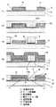
図1は、本発明の第1の実施の形態によるCCD固体撮像素子の画素周辺部の製造工程を示す断面図である。なお、図1はCCD固体撮像素子の水平転送方向の断面を示しているが、垂直転送方向についてもほぼ同様の構造を有しているものとする。以下、この図1に沿って本実施の形態によるCCD固体撮像素子の製造方法について説明する。
なお、CCD固体撮像素子の全体構成については上記従来の技術で説明したものと同様であるので説明は省略する。
まず、図1(1)において、半導体基板11にはフォトダイオードやCCD垂直転送部(ともに図示せず)が設けられている。
そして、この半導体基板11の上面にはゲート絶縁膜(シリコン酸化膜)12が設けられ、このゲート絶縁膜12上のCCD垂直転送部に対応する領域にポリシリコンよりなる転送電極13が設けられている。
また、この転送電極13の表面には絶縁膜14が設けられているが、この絶縁膜14は、例えば転送電極13の直接酸化によって形成された酸化シリコン膜である。
【0023】
次に、図1(2)では、全面に低反射膜材料15Aを所定の膜厚で積層し、その上層全面に平坦化膜材料16Aを積層する。ここで低反射膜材料15Aとしては窒化シリコン膜をCVD等によって所定の膜厚に積層し、平坦化膜材料16Aとしては酸化シリコン膜をCVD等によって所定の膜厚に積層した後、その上面を平坦化する。なお、この場合の平坦化方法には、CMP(化学機械研磨)等を用いることができる。
次に、図1(3)では、フォトレジストおよびエッチング工程により、フォトダイオードの受光領域を残して低反射膜材料15Aと平坦化膜材料16Aを除去する。これにより、図1(3)に示すように、フォトダイオードの受光領域のパターン形状に対応した低反射膜15および平坦化膜16が形成される。これにより、低反射膜15および平坦化膜16と転送電極13および絶縁膜14との間の間隙部には、ゲート絶縁膜12が露出された状態となる。なお、この場合のエッチングは、低反射膜15および平坦化膜16がシリコン系の材料であるので深さの制御は容易に行うことができる。
【0024】
次に、図1(4)では、その上面全体にアルミニウムや高融点金属等の遮光膜材17AをCVD等によって積層する。これにより、低反射膜15および平坦化膜16と転送電極13および絶縁膜14との間の間隙部に遮光膜材17Aが充填され、フォトダイオードの受光領域に対応した低反射膜15および平坦化膜16の外周部にガイドされた状態で、遮光膜17の開口部17Bとなる部分が形成されるとともに、開口部17Bの内周下面部がゲート絶縁膜12に直接当接した状態で配置される。
次に、図1(5)では、遮光膜材17Aおよび平坦化膜16の上面をCMPによって研磨し、平坦化膜16の上面が完全に露出するように遮光膜材17Aを除去して遮光膜17を完成する。これにより、遮光膜17および平坦化膜16の上面は、面一の平坦面に仕上げられる。
なお、この後、その上層に各種配線層や層間絶縁層、さらには平坦化膜(層内レンズを含む)等を形成した後、オンチップフィルタやオンチップマイクロレンズ等の装着を行うが、これらは本発明と職接関係しないため説明は省略する。
【0025】
以上のような工程によって作製されたCCD固体撮像素子においては、遮光膜17の開口部17Bの内周部がエッチングにより形成されるものではないため、下地を保護するための膜が必要なく、従来例におけるCVDシリコン絶縁膜5が必要ない。
そのため、遮光膜17の開口部17Bの下面部と半導体基板11との間隔が従来例に比べて短縮でき、スミアの原因となる斜めの光の入射を抑えることが可能となる。
さらに、低反射膜15は開口部17Bの全面に配置されており、低反射膜15の効果を最大限に発揮することができるため、反射光の再入射量を抑制でき、感度を向上することが可能である。また、この低反射膜15は、遮光膜17の開口内周部と重なることもなく、スミア特性を悪化させることはない。
【0026】
したがって、本実施の形態では、遮光膜17の開口部17Bの下面部と半導体基板11との間隔を縮小して、斜めの光の電荷転送部への入射を抑えることでき、スミアの発生を低減することができる。
また、フォトダイオードの受光領域に形成される低反射膜15の外縁部を遮光膜17の開口部内縁部と重なることなく配置でき、かつ、低反射膜15を開口部17Bの全面に形成することができ、フォトダイオードの受光面における乱反射を有効に防止して、スミア特性を悪化させることなく、感度を向上することができる。
【0027】
なお、上述のようにゲート絶縁膜上に遮光膜の端部が直接接触する状態で記載されているものについては、過去の特許出願の明細書や図面等において記載されたものも存在するが、実際に製造される固体撮像素子では、遮光膜のエッチング工程に伴い、低反射膜の上に絶縁膜を設けることが必要となるため、図1(Z)に示す固体撮像素子を得るためには、本発明に固有の製造方法を用いることが必要となる。
したがって、本発明は固体撮像素子の製造方法に加えて、このような製造方法によって形成される固体撮像素子の構造も本発明に特有のものであり、本発明に含まれるものとする。
【0028】
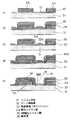
図2は、本発明の第2の実施の形態によるCCD固体撮像素子の画素周辺部の製造工程を示す断面図である。なお、図2はCCD固体撮像素子の水平転送方向の断面を示しているが、垂直転送方向についてもほぼ同様の構造を有しているものとする。以下、この図2に沿って本実施の形態によるCCD固体撮像素子の製造方法について説明する。
まず、図2(1)において、半導体基板21にはフォトダイオードやCCD垂直転送部(ともに図示せず)が設けられている。
そして、この半導体基板21の上面にはゲート絶縁膜(シリコン酸化膜)22が設けられ、このゲート絶縁膜22上のCCD垂直転送部に対応する領域にポリシリコンよりなる転送電極23が設けられている。
また、この転送電極23の上面には、CVD等によって積層されたシリコン酸化膜等の絶縁膜24が設けられている。この絶縁膜24は、後述するエッチバックによるコンタクト形成時のエッチング保護膜となるものである。
次に、図2(2)において、転送電極23及び絶縁膜24の表面を熱酸化し、酸化シリコン膜による絶縁膜25を形成する。すなわち、本例では、CVDシリコン酸化膜による絶縁膜24と熱酸化シリコン膜による絶縁膜25の複合絶縁膜で転送電極23を包囲している。
【0029】
次に、図2(3)では、全面に低反射膜材料26Aを所定の膜厚で積層し、その上層全面に平坦化膜材料27Aを積層する。ここで低反射膜材料26Aとしては窒化シリコン膜をCVD等によって所定の膜厚に積層し、平坦化膜材料27Aとしては酸化シリコン膜をCVD等によって所定の膜厚に積層した後、その上面を平坦化する。なお、この場合の平坦化方法には、CMP(化学機械研磨)等を用いることができる。
次に、図2(4)では、フォトレジストおよびエッチング工程により、フォトダイオードの受光領域を残して平坦化膜材料27Aを除去し、次いで図2(5)では、フォトダイオードの受光領域を残して低反射膜材料26Aを除去する。これにより、フォトダイオードの受光領域のパターン形状に対応した低反射膜26および平坦化膜27が形成される。
これにより、低反射膜26および平坦化膜27と転送電極23および絶縁膜25との間の間隙部には、ゲート絶縁膜22が露出された状態となる。
【0030】
次に、図2(6)に示すように、エッチバック(全面ドライエッチング)を行い、このエッチバックによってゲート絶縁膜22の露出部分に溝部22Aを形成し、この溝部22Aより半導体基板の表面を露出させる。
すなわち、この溝部22Aは、受光領域上の低反射膜26および平坦化膜27と転送電極23の上面の絶縁膜24、25をマスクとするエッチングによって形成される。この際、絶縁膜24、25の複合膜が転送電極23の保護膜として有効に機能する。
【0031】
次に、図2(7)では、その上面全体にアルミニウムや高融点金属等の遮光膜材28AをCVD等によって積層する。
これにより、低反射膜26および平坦化膜27と転送電極23および絶縁膜24、25との間の間隙部、ならびにゲート絶縁膜22に形成した溝部22Aに遮光膜材28Aが充填され、フォトダイオードの受光領域に対応した低反射膜26および平坦化膜27の外周部にガイドされた状態で、遮光膜28の開口部28Bとなる部分が形成されるとともに、開口部28Bの内周下面部が半導体基板21の表面に直接当接した状態で配置される。
次に、図2(8)では、遮光膜材28Aおよび平坦化膜27の上面をCMPによって研磨し、平坦化膜27の上面が完全に露出するように遮光膜材28Aを除去して遮光膜28を完成する。これにより、遮光膜28および平坦化膜27の上面は、面一の平坦面に仕上げられる。
なお、この後、その上層に各種配線層や層間絶縁層、さらには平坦化膜(層内レンズを含む)等を形成した後、オンチップフィルタやオンチップマイクロレンズ等の装着を行うが、これらは本発明と職接関係しないため説明は省略する。
【0032】
以上のような工程によって作製されたCCD固体撮像素子においては、遮光膜28の開口部28Bの内周部がエッチングにより形成されるものではないため、下地を保護するための膜が必要なく、従来例におけるCVDシリコン絶縁膜5が必要ない。
そのため、遮光膜28の開口部28Bの下面部と半導体基板21との間隔が従来例に比べて短縮でき、スミアの原因となる斜めの光の入射を抑えることが可能となる。
さらに、低反射膜26は開口部28Bの全面に配置されており、低反射膜26の効果を最大限に発揮することができるため、反射光の再入射量を抑制でき、感度を向上することが可能である。また、この低反射膜26は、遮光膜28の開口内周部と重なることもなく、スミア特性を悪化させることはない。
【0033】
したがって、本実施の形態では、遮光膜28の開口部28Bの下面部と半導体基板21との間隔を縮小して、斜めの光の電荷転送部への入射を抑えることでき、スミアの発生を低減することができる。
また、フォトダイオードの受光領域に形成される低反射膜26の外縁部を遮光膜28の開口部内縁部と重なることなく配置でき、かつ、低反射膜26を開口部28Bの全面に形成することができ、フォトダイオードの受光面における乱反射を有効に防止して、スミア特性を悪化させることなく、感度を向上することができる。
さらに、遮光膜28の開口部28Bの下面部を半導体基板21の表面を直接当接させて導通させたことから、半導体基板21および遮光膜28の電位を安定化することが可能となり、読み出し電圧の低減や、飽和信号のムラやニー特性を改善を図ることができる。
【0034】
図3は、本発明の第3の実施の形態によるCCD固体撮像素子の画素周辺部の製造工程を示す断面図である。なお、図3はCCD固体撮像素子の水平転送方向の断面を示しているが、垂直転送方向についてもほぼ同様の構造を有しているものとする。以下、この図3に沿って本実施の形態によるCCD固体撮像素子の製造方法について説明する。
本実施の形態は、上述した従来例と同様に、エッチングによって遮光膜に開口部を形成するものであるが、遮光膜の形成に先立って受光領域上の透明絶縁膜を工夫することにより、受光領域の周辺部分で遮光膜の開口部下面部がフォトダイオード(基板)の表面に直接接触した遮光構造を形成できるようにしたものである。
【0035】
まず、図3(1)において、半導体基板31にはフォトダイオードやCCD垂直転送部(ともに図示せず)が設けられている。
そして、この半導体基板31の上面にはゲート絶縁膜(シリコン酸化膜)32が設けられ、このゲート絶縁膜32上のCCD垂直転送部に対応する領域にポリシリコンよりなる転送電極33が設けられている。
次に、転送電極33の表面を熱酸化し、酸化シリコン膜による絶縁膜34を形成する。
【0036】
次に、図3(2)において、全面に遮光膜下の層間絶縁膜となる透明絶縁膜35を形成するが、この透明絶縁膜35を、SiH4 又はO2 を反応ガスとする常圧CVD法で形成することにより、図示のように、フォトダイオードの上部領域では、中央部で膜厚が大きく、外周側に向かって膜厚が小さくなり、転送電極33に近接する部分で薄い状態となる。
次に、透明絶縁膜35に対して全面エッチバックを行う。
図3(3)は、この全面エッチバック後の状態を示している。図示のように、撮像領域全体を均一に異方性を有する条件で、適切な膜厚だけCVD酸化シリコン膜(透明絶縁膜)35をエッチバックすることにより、膜厚の薄い転送電極33に近接する部分(すなわち、受光領域の外周領域)において、CVD酸化シリコン膜35及び、ゲート絶縁膜32が除去され、フォトダイオード表面のP型不純物層を露出させることができる(露出部31A)。
一方、フォトダイオードの受光領域の中央部にはCVD酸化シリコン膜35が残っている(残膜部35A)。
【0037】
この後、図3(4)に示すように、全面に遮光膜材36Aを形成した後、図3(5)に示すように、開口部36Bを形成する部分の遮光膜材36Aをエッチングによって除去し、遮光膜36を形成する。このとき、開口部36Bとなる部分のフォトダイオードの受光領域の表面には、上述したCVD酸化シリコン膜35が残っているため、遮光膜材36Aのエッチング時に下地は十分に保護されることになる。
また、転送電極33に近接する部分(すなわち、受光領域の外周領域)においては、遮光膜36の開口部36Bの下面部分がコンタクトとなってフォトダイオード表面のP型半導体層と導通しており、安定した電位に保持することができるので、読み出し電圧の低減や、飽和信号のムラやニー特性の改善を図ることができる。
そして、このようなコンタクト構造は、上述した全面エッチバック処理において、転送電極33のセルフアラインによって形成することができるので、フォトリソドグラフィによるレジストマスク等を用いることなく形成でき、フォトリソドグラフィの解像度や重ね合わせ精度に依存することなく、高精度のコンタクトを容易に作成できる利点がある。
また、このような遮光膜36によるコンタクト構造によってフォトダイオードの受光領域の周辺部分が確実に遮光され、斜めの入射光を適正に遮光でき、スミア等を有効に抑制できる。
【0038】
なお、本発明にかかる固体撮像素子の製造方法および固体撮像素子は、上記図1〜図3に示す構成のものに限定されず、本発明の要旨を逸脱しない範囲で種々の変形が可能である。
例えば、上述した例では、2次元画素配列のCCD固体撮像素子を前提として説明したが、本発明は、それ以外の固体撮像素子についても同様に適用し得るものである。
また、上述した例では、反射防止用の低反射膜15を有する場合を説明したが、このような低反射膜15を設けず、一体の透明絶縁膜を平坦化膜として設けるような構成であってもよい。
さらに、上述した各層の膜種や加工方法等は適宜変形が可能なものである。
【0039】
【発明の効果】
以上のように、本発明による固体撮像素子の製造方法によれば、半導体基板に形成したゲート絶縁膜上の少なくとも光電変換素子に対応する領域に透明絶縁膜を形成し、この透明絶縁膜をエッチングすることにより、光電変換素子の受光領域上に透明絶縁膜を残すとともに、受光領域の外周に位置する部分の透明絶縁膜及びゲート絶縁膜を除去して半導体基板を露出させ、その後、半導体基板の略全面に遮光膜材を積層し、受光領域上に積層された遮光膜材を除去することにより、光電変換素子の受光領域に対応する開口部を備えた遮光膜を形成することから、受光領域の外周に位置する部分に遮光膜を適正かつ容易に配置でき、さらに遮光膜の開口部の下面部を半導体基板に直接接触した状態で配置することができる。
したがって、遮光膜の下面部と半導体基板が絶縁膜を介さずに直接接触する遮光構造により、受光領域への斜めの入射光を有効に遮光することができ、このような不正な入射光によるスミア特性の劣化を防止することが可能な遮光構造を得ることができる。
また、遮光膜と半導体基板とを容易に導通させることができ、電気的に安定した状態を得ることができる。
【0040】
また、本発明による固体撮像素子によれば、受光領域の外周に位置する部分に遮光膜が適正に配置され、かつ、遮光膜の開口部の下面部が半導体基板に直接接触した状態で配置される遮光構造となる。
したがって、遮光膜の下面部と半導体基板が絶縁膜を介さずに直接接触する遮光構造により、受光領域への斜めの入射光を有効に遮光することができ、このような不正な入射光によるスミア特性の劣化を防止することが可能な遮光構造を得ることができる。
また、遮光膜と半導体基板とを容易に導通させることができ、電気的に安定した状態を得ることができる。
【図面の簡単な説明】
【図1】 本発明の第1の実施の形態によるCCD固体撮像素子の画素周辺部の製造工程を示す断面図である。
【図2】 本発明の第2の実施の形態によるCCD固体撮像素子の画素周辺部の製造工程を示す断面図である。
【図3】 本発明の第3の実施の形態によるCCD固体撮像素子の画素周辺部の製造工程を示す断面図である。
【図4】 従来のCCD固体撮像素子の画素周辺部の製造工程を示す断面図である。
【符号の説明】
11、21、31……半導体基板、12、22、32……ゲート絶縁膜、13、23、33……転送電極、14、24、25、34……絶縁膜、15、26……低反射膜、16、27……平坦化膜、17、28、36……遮光膜、17B、28B、36B……開口部、35……CVD酸化シリコン膜。[0001]
BACKGROUND OF THE INVENTION
The present invention relates to a method for manufacturing a solid-state imaging device in which a low-reflection film for preventing reflection is provided in a light receiving region of a photoelectric conversion device, and a solid-state imaging device.
[0002]
[Prior art]
Conventionally, in a CCD solid-state imaging device, signal charges corresponding to the amount of incident light are generated and stored by a plurality of photodiodes (photoelectric conversion elements) formed on a semiconductor substrate, and the signal charges generated and stored by the photodiodes are stored. This signal charge is converted into an electrical signal and output by being transferred to the outside by a charge transfer unit having a CCD structure.
Each of the plurality of photodiodes constitutes a unit pixel and is provided in a two-dimensional array on the semiconductor substrate. A charge transfer unit is provided for each column of each photodiode, and reads the signal charge of each photodiode. A plurality of vertical transfer units that transfer in the vertical direction and one or a plurality of horizontal transfer units that transfer the signal charges transferred by each vertical transfer unit in the horizontal direction.
The output stage of the horizontal transfer unit is provided with an output unit having a charge-voltage (current) conversion function and an amplification function, and the signal charge transferred by the horizontal transfer unit is sequentially converted into an electric signal to be a subsequent signal. Output to the processing circuit.
[0003]
Further, on the semiconductor substrate on which each of such elements is formed, a transfer electrode corresponding to the charge transfer unit, a light shielding film for shielding a region other than the light receiving region of the photodiode, and the like are formed via an insulating film, Various wiring layers, a planarizing film, and the like are formed on the upper layer, and an on-chip color filter, an on-chip microlens, and the like are further provided on the upper layer.
The light receiving area of the photodiode is provided with a low reflection film which is an antireflection film for suppressing generation of reflected light in the light receiving area and preventing image quality disturbance due to re-incidence of the reflected light.
[0004]
FIG. 4 is a cross-sectional view showing a manufacturing process of a pixel peripheral portion of a conventional CCD solid-state imaging device having the above-described configuration. Hereinafter, a conventional method for manufacturing a CCD solid-state imaging device will be described with reference to FIG.
First, in FIG. 4A, the
A gate insulating film (silicon oxide film) 2 is provided on the upper surface of the
An
[0005]
Next, in FIG. 4B, a low reflection film (silicon nitride film) 6 is provided in a region corresponding to the light receiving region on the
Thereafter, in FIG. 4 (3), a light-shielding film material (aluminum or refractory metal or the like) is laminated on the entire surface with a predetermined film thickness, and then, as shown in FIG. The light shielding film material is removed by photoresist and etching to complete the
After this, after forming various wiring layers, interlayer insulating layers, and planarization films (including intra-layer lenses) on the upper layer, on-chip filters and on-chip microlenses are mounted. Since this is not directly related to the problem to be solved by the present invention, its description is omitted.
[0006]
[Problems to be solved by the invention]
However, the conventional solid-state imaging device has a structure in which the
In order to reduce such smear, it is necessary to make the
However, the
[0007]
The
Therefore, if the
[0008]
In addition, in the specifications and drawings of past patent applications related to this type of solid-state imaging device, there are also those described in a state where the end of the light shielding film is in direct contact with the gate insulating film, In order to simplify the description of the invention, the
[0009]
SUMMARY OF THE INVENTION An object of the present invention is to provide a method for manufacturing a solid-state imaging device and a solid-state imaging device capable of preventing deterioration of smear characteristics due to oblique incident light.
[0010]
[Means for Solving the Problems]
To achieve the above objective,The solid-state imaging device manufacturing method of the present invention includes a first step of forming a photoelectric conversion element and a charge transfer unit on a semiconductor substrate, a second step of forming a gate insulating film on the upper surface of the semiconductor substrate,
A third step of forming a transfer electrode in a region corresponding to the charge transfer portion on the gate insulating film, and forming an insulating film on a surface of the transfer electrode; and at least the photoelectric conversion element on the gate insulating film A fourth step of forming a transparent insulating film in a corresponding region; and etching the transparent insulating film to leave a transparent insulating film on the light receiving region of the photoelectric conversion element and to be positioned on the outer periphery of the light receiving region A fifth step of removing the transparent insulating film and the gate insulating film of the portion to expose the semiconductor substrate; and a light shielding film material is laminated on substantially the entire surface of the semiconductor substrate, and laminated at least on the light receiving region of the photoelectric conversion element. Forming a light shielding film having an opening corresponding to the light receiving region of the photoelectric conversion element by removing the light shielding film material, and in the fourth step, the transparent insulation The film thickness at the center of the light receiving region of the photoelectric conversion element is large, and wherein the film thickness at a portion located on the outer periphery of the light receiving area is small.
[0011]
In the present invention, the sixth step forms a light shielding structure in which the light shielding film and the semiconductor substrate are arranged in a state in which the light shielding film and the semiconductor substrate are in direct contact with each other at a portion located on the outer periphery of the light receiving region of the photoelectric conversion element. Features.
[0012]
In the present invention, the transparent insulating film may be SiH.4Or O2It is formed by an atmospheric pressure CVD method in a gas atmosphere.
[0013]
Moreover, the solid-state imaging device of the present invention isA semiconductor substrate is provided with a photoelectric conversion element that generates and accumulates charges corresponding to at least incident light, and a charge transfer unit that transfers signal charges generated and accumulated by the photoelectric conversion elements, and is provided on the semiconductor substrate. At least a transfer electrode for the charge transfer unit via a gate insulating film and a light shielding film having an opening corresponding to the light receiving region of the photoelectric conversion element are provided, and further, the photoelectric conversion element on the gate insulating film A transparent insulating film is provided in a region corresponding to the light receiving region, and the transparent insulating film is formed so that the film thickness gradually decreases from the central portion of the light receiving region of the photoelectric conversion element toward the outer peripheral side, and the transparent insulating film and The gate insulating film is removed at the portion located on the outer periphery of the light receiving region of the photoelectric conversion element,The light shielding film is a lower surface portion located on the outer periphery of the light receiving region.The semiconductor substrate is disposed in direct contact with the semiconductor substrate.
[0014]
In the present invention, the transparent insulating film may be SiH.4Or O2It is formed by an atmospheric pressure CVD method in a gas atmosphere.
[0015]
In the method for manufacturing a solid-state imaging device according to the present invention, a transparent insulating film is formed on at least a region corresponding to the photoelectric conversion element on the gate insulating film formed on the semiconductor substrate, and the transparent insulating film is etched to thereby obtain the photoelectric conversion element. The transparent insulating film is left on the light receiving region, the transparent insulating film and the gate insulating film located on the outer periphery of the light receiving region are removed to expose the semiconductor substrate, and then the light shielding film material is applied to substantially the entire surface of the semiconductor substrate. A light shielding film having an opening corresponding to the light receiving area of the photoelectric conversion element is formed by removing the light shielding film material stacked and stacked on the light receiving area. The light shielding film can be disposed appropriately and easily, and further, the lower surface portion of the opening of the light shielding film can be disposed in direct contact with the semiconductor substrate.
[0016]
Therefore, the oblique light incident on the light receiving region can be effectively shielded by the light shielding structure in which the lower surface portion of the light shielding film and the semiconductor substrate are in direct contact with each other without an insulating film. A light shielding structure capable of preventing the deterioration of characteristics can be obtained.
[0017]
Further, the light shielding film and the semiconductor substrate can be easily conducted, and an electrically stable state can be obtained.
[0018]
Further, in the solid-state imaging device according to the present invention, the light shielding film is appropriately disposed in the portion located on the outer periphery of the light receiving region, and the light shielding is disposed in a state where the lower surface portion of the opening of the light shielding film is in direct contact with the semiconductor substrate. It has a structure.
[0019]
Therefore, the oblique light incident on the light receiving region can be effectively shielded by the light shielding structure in which the lower surface portion of the light shielding film and the semiconductor substrate are in direct contact with each other without an insulating film. A light shielding structure capable of preventing the deterioration of characteristics can be obtained.
[0020]
Further, the light shielding film and the semiconductor substrate can be easily conducted, and an electrically stable state can be obtained.
[0021]
DETAILED DESCRIPTION OF THE INVENTION
Hereinafter, embodiments of the present invention will be described in detail with reference to the drawings.
The embodiments described below are preferred specific examples of the present invention, and various technically preferable limitations are given. However, the scope of the present invention is not limited to the following description. Unless otherwise specified, the present invention is not limited to these embodiments.
[0022]
FIG. 1 is a cross-sectional view showing a manufacturing process of a pixel peripheral portion of a CCD solid-state imaging device according to a first embodiment of the present invention. 1 shows a cross section of the CCD solid-state imaging device in the horizontal transfer direction, it is assumed that the vertical transfer direction has substantially the same structure. A method for manufacturing the CCD solid-state imaging device according to this embodiment will be described below with reference to FIG.
The overall configuration of the CCD solid-state imaging device is the same as that described in the above prior art, and the description thereof is omitted.
First, in FIG. 1A, a semiconductor substrate 11 is provided with a photodiode and a CCD vertical transfer unit (both not shown).
A gate insulating film (silicon oxide film) 12 is provided on the upper surface of the semiconductor substrate 11, and a
An insulating
[0023]
Next, in FIG. 1B, the low
Next, in FIG. 1C, the low
[0024]
Next, in FIG. 1 (4), a light
Next, in FIG. 1 (5), the upper surfaces of the light
After this, after forming various wiring layers, interlayer insulating layers, and planarization films (including intra-layer lenses) on the upper layer, on-chip filters and on-chip microlenses are mounted. Is not related to the present invention, so the description is omitted.
[0025]
In the CCD solid-state imaging device manufactured by the process as described above, the inner peripheral portion of the opening 17B of the
Therefore, the distance between the lower surface portion of the opening 17B of the
Furthermore, since the
[0026]
Therefore, in the present embodiment, the distance between the lower surface portion of the opening 17B of the
Further, the outer edge portion of the
[0027]
In addition, as described above, what is described in a state in which the end portion of the light shielding film is in direct contact with the gate insulating film, there are those described in the specification and drawings of the past patent application, In an actually manufactured solid-state imaging device, it is necessary to provide an insulating film on the low-reflection film along with the etching process of the light-shielding film. Therefore, in order to obtain the solid-state imaging device shown in FIG. Therefore, it is necessary to use a manufacturing method unique to the present invention.
Therefore, in addition to the manufacturing method of a solid-state image sensor, the present invention also includes a structure of a solid-state image sensor formed by such a manufacturing method, which is unique to the present invention, and is included in the present invention.
[0028]
FIG. 2 is a cross-sectional view showing a manufacturing process of a pixel peripheral portion of a CCD solid-state imaging device according to the second embodiment of the present invention. FIG. 2 shows a cross section of the CCD solid-state imaging device in the horizontal transfer direction, but it is assumed that the vertical transfer direction has substantially the same structure. Hereinafter, the manufacturing method of the CCD solid-state imaging device according to the present embodiment will be described with reference to FIG.
First, in FIG. 2A, the
A gate insulating film (silicon oxide film) 22 is provided on the upper surface of the
Further, an insulating
Next, in FIG. 2B, the surfaces of the
[0029]
Next, in FIG. 2C, the low
Next, in FIG. 2 (4), the
As a result, the
[0030]
Next, as shown in FIG. 2 (6), etch back (entire dry etching) is performed, and the
That is, the
[0031]
Next, in FIG. 2 (7), a light
Thus, the light
Next, in FIG. 2 (8), the upper surfaces of the light
After this, after forming various wiring layers, interlayer insulating layers, and planarization films (including intra-layer lenses) on the upper layer, on-chip filters and on-chip microlenses are mounted. Is not related to the present invention, so the description is omitted.
[0032]
In the CCD solid-state imaging device manufactured by the process as described above, the inner peripheral portion of the
Therefore, the distance between the lower surface portion of the
Further, since the
[0033]
Therefore, in the present embodiment, the distance between the lower surface portion of the
Further, the outer edge of the
Further, since the lower surface of the
[0034]
FIG. 3 is a cross-sectional view showing a manufacturing process of a pixel peripheral portion of a CCD solid-state imaging device according to a third embodiment of the present invention. 3 shows a cross section in the horizontal transfer direction of the CCD solid-state imaging device, it is assumed that the vertical transfer direction has substantially the same structure. A method for manufacturing the CCD solid-state imaging device according to this embodiment will be described below with reference to FIG.
In the present embodiment, as in the conventional example described above, an opening is formed in the light shielding film by etching. However, prior to the formation of the light shielding film, the transparent insulating film on the light receiving region is devised to receive light. A light shielding structure in which the lower surface of the opening of the light shielding film is in direct contact with the surface of the photodiode (substrate) in the peripheral portion of the region can be formed.
[0035]
First, in FIG. 3A, the
A gate insulating film (silicon oxide film) 32 is provided on the upper surface of the
Next, the surface of the
[0036]
Next, in FIG. 3B, a transparent insulating
Next, the entire surface of the transparent insulating
FIG. 3 (3) shows a state after this entire surface etch back. As shown in the figure, by etching back the CVD silicon oxide film (transparent insulating film) 35 by an appropriate film thickness under the condition that the entire imaging region has a uniform anisotropy, it is close to the
On the other hand, the CVD
[0037]
Thereafter, as shown in FIG. 3 (4), after the light
In addition, in the portion close to the transfer electrode 33 (that is, the outer peripheral region of the light receiving region), the lower surface portion of the opening portion 36B of the
Such a contact structure can be formed by self-alignment of the
In addition, such a contact structure with the
[0038]
The solid-state imaging device manufacturing method and the solid-state imaging device according to the present invention are not limited to the configurations shown in FIGS. 1 to 3, and various modifications can be made without departing from the gist of the present invention. .
For example, in the above-described example, the description has been made on the premise of a CCD solid-state imaging device having a two-dimensional pixel array, but the present invention can be similarly applied to other solid-state imaging devices.
In the above-described example, the case where the antireflection
Furthermore, the above-described film types, processing methods, and the like of each layer can be modified as appropriate.
[0039]
【The invention's effect】
As described above, according to the method for manufacturing a solid-state imaging device according to the present invention,A transparent insulating film is formed on at least a region corresponding to the photoelectric conversion element on the gate insulating film formed on the semiconductor substrate, and the transparent insulating film is etched to leave the transparent insulating film on the light receiving region of the photoelectric conversion element. The transparent insulating film and the gate insulating film in the outer periphery of the light receiving region are removed to expose the semiconductor substrate, and then a light shielding film material is laminated on the substantially entire surface of the semiconductor substrate, and the light shielding laminated on the light receiving region. By removing the film material, a light-shielding film having an opening corresponding to the light-receiving area of the photoelectric conversion element is formed, so that the light-shielding film can be appropriately and easily disposed in a portion located on the outer periphery of the light-receiving area. The lower surface portion of the opening of the light shielding film can be disposed in direct contact with the semiconductor substrate.
Therefore, the oblique light incident on the light receiving region can be effectively shielded by the light shielding structure in which the lower surface portion of the light shielding film and the semiconductor substrate are in direct contact with each other without an insulating film. A light shielding structure capable of preventing the deterioration of characteristics can be obtained.
Further, the light shielding film and the semiconductor substrate can be easily conducted, and an electrically stable state can be obtained.
[0040]
Also,According to the solid-state imaging device according to the present invention, the light-shielding film is appropriately disposed in the portion located on the outer periphery of the light-receiving region, and the light-shielding is disposed in a state where the lower surface portion of the opening of the light-shielding film is in direct contact with the semiconductor substrate It becomes a structure.
Therefore, the oblique light incident on the light receiving region can be effectively shielded by the light shielding structure in which the lower surface portion of the light shielding film and the semiconductor substrate are in direct contact with each other without an insulating film. A light shielding structure capable of preventing the deterioration of characteristics can be obtained.
Further, the light shielding film and the semiconductor substrate can be easily conducted, and an electrically stable state can be obtained.
[Brief description of the drawings]
FIG. 1 is a cross-sectional view showing a manufacturing process of a pixel peripheral portion of a CCD solid-state imaging device according to a first embodiment of the present invention.
FIG. 2 is a cross-sectional view showing a manufacturing process of a pixel peripheral portion of a CCD solid-state imaging device according to a second embodiment of the present invention.
FIG. 3 is a cross-sectional view showing a manufacturing process of a pixel peripheral portion of a CCD solid-state imaging device according to a third embodiment of the present invention.
FIG. 4 is a cross-sectional view showing a manufacturing process of a pixel peripheral portion of a conventional CCD solid-state imaging device.
[Explanation of symbols]
11, 21, 31 ... Semiconductor substrate, 12, 22, 32 ... Gate insulating film, 13, 23, 33 ... Transfer electrode, 14, 24, 25, 34 ... Insulating film, 15, 26 ...
Claims (5)
Translated fromJapanese前記半導体基板の上面にゲート絶縁膜を形成する第2の工程と、
前記ゲート絶縁膜上の前記電荷転送部に対応する領域に転送電極を形成し、前記転送電極の表面に絶縁膜を形成する第3の工程と、
前記ゲート絶縁膜上の少なくとも前記光電変換素子に対応する領域に透明絶縁膜を形成する第4の工程と、
前記透明絶縁膜をエッチングすることにより、前記光電変換素子の受光領域上に透明絶縁膜を残すとともに、前記受光領域の外周に位置する部分の透明絶縁膜及びゲート絶縁膜を除去して前記半導体基板を露出させる第5の工程と、
前記半導体基板の略全面に遮光膜材を積層し、少なくとも前記光電変換素子の受光領域上に積層された遮光膜材を除去することにより、前記光電変換素子の受光領域に対応する開口部を備えた遮光膜を形成する第6の工程とを有し、
前記第4の工程において、前記透明絶縁膜は、前記光電変換素子の受光領域の中央部で膜厚が大きく、受光領域の外周に位置する部分で膜厚が小さい、
ことを特徴とする固体撮像素子の製造方法。A first step of forming a photoelectric conversion element and a charge transfer unit on a semiconductor substrate;
A second step of forming a gate insulating film on the upper surface of the semiconductor substrate;
A third step of forming a transfer electrode in a region corresponding to the charge transfer portion on the gate insulating film, and forming an insulating film on a surface of the transfer electrode;
A fourth step of forming a transparent insulating film in a region corresponding to at least the photoelectric conversion element on the gate insulating film;
Etching the transparent insulating film leaves a transparent insulating film on the light receiving region of the photoelectric conversion element, and removes a portion of the transparent insulating film and gate insulating film located on the outer periphery of the light receiving region to remove the semiconductor substrate. A fifth step of exposing
A light shielding film material is laminated on substantially the entire surface of the semiconductor substrate, and at least the light shielding film material laminated on the light receiving region of the photoelectric conversion element is removed, thereby providing an opening corresponding to the light receiving region of the photoelectric conversion element. shielding filmhave a a sixth step of formingwas,
In the fourth step, the transparent insulating film has a large film thickness at the center of the light receiving region of the photoelectric conversion element and a small film thickness at a portion located on the outer periphery of the light receiving region.
A method for manufacturing a solid-state imaging device.
前記半導体基板上に少なくともゲート絶縁膜を介して前記電荷転送部用の転送電極と、前記光電変換素子の受光領域に対応する開口部を備えた遮光膜とが設けられ、
さらに前記ゲート絶縁膜上の光電変換素子の受光領域に対応する領域に透明絶縁膜を有し、
前記透明絶縁膜が光電変換素子の受光領域の中央部から外周側に向かって徐々に膜厚が小さく形成されるとともに、前記透明絶縁膜及びゲート絶縁膜が光電変換素子の受光領域の外周に位置する部分で除去され、
前記遮光膜が前記受光領域の外周に位置する下面部分で前記半導体基板に直接接触した状態で配置される、
ことを特徴とする固体撮像素子。The semiconductor substrate is provided with a photoelectric conversion element that generates and accumulates charges according to at least incident light, and a charge transfer unit that transfers signal charges generated and accumulated by the photoelectric conversion elements,
A transfer electrode for the charge transfer unit and a light shielding film having an opening corresponding to a light receiving region of the photoelectric conversion element are provided on the semiconductor substrate via at least a gate insulating film,
Furthermore, a transparent insulating film is provided in a region corresponding to the light receiving region of the photoelectric conversion element on the gate insulating film,
The transparent insulating film is formed to gradually decrease in thickness from the center of the light receiving region of the photoelectric conversion element toward the outer peripheral side, and the transparent insulating film and the gate insulating film are positioned on the outer periphery of the light receiving region of the photoelectric conversion element. To be removed
The light-shielding filmis disposed in a state in which the light-shielding filmis in direct contact with the semiconductor substrateat a lower surface portion located on the outer periphery of the light-receiving region .
The solid-state image sensor characterized by the above-mentioned.
Priority Applications (1)
| Application Number | Priority Date | Filing Date | Title |
|---|---|---|---|
| JP2002352770AJP4449298B2 (en) | 2002-03-06 | 2002-12-04 | Solid-state image sensor manufacturing method and solid-state image sensor |
Applications Claiming Priority (3)
| Application Number | Priority Date | Filing Date | Title |
|---|---|---|---|
| JP2002060770 | 2002-03-06 | ||
| JP2002243053 | 2002-08-23 | ||
| JP2002352770AJP4449298B2 (en) | 2002-03-06 | 2002-12-04 | Solid-state image sensor manufacturing method and solid-state image sensor |
Publications (2)
| Publication Number | Publication Date |
|---|---|
| JP2004140309A JP2004140309A (en) | 2004-05-13 |
| JP4449298B2true JP4449298B2 (en) | 2010-04-14 |
Family
ID=32475128
Family Applications (1)
| Application Number | Title | Priority Date | Filing Date |
|---|---|---|---|
| JP2002352770AExpired - Fee RelatedJP4449298B2 (en) | 2002-03-06 | 2002-12-04 | Solid-state image sensor manufacturing method and solid-state image sensor |
Country Status (1)
| Country | Link |
|---|---|
| JP (1) | JP4449298B2 (en) |
Families Citing this family (3)
| Publication number | Priority date | Publication date | Assignee | Title |
|---|---|---|---|---|
| JP2007080941A (en) | 2005-09-12 | 2007-03-29 | Fujifilm Corp | Solid-state imaging device and manufacturing method thereof |
| WO2010116974A1 (en) | 2009-04-07 | 2010-10-14 | ローム株式会社 | Photoelectric conversion device and image pickup device |
| JP7603382B2 (en)* | 2019-11-18 | 2024-12-20 | ソニーセミコンダクタソリューションズ株式会社 | Image pickup device and method for manufacturing image pickup device |
- 2002
- 2002-12-04JPJP2002352770Apatent/JP4449298B2/ennot_activeExpired - Fee Related
Also Published As
| Publication number | Publication date |
|---|---|
| JP2004140309A (en) | 2004-05-13 |
Similar Documents
| Publication | Publication Date | Title |
|---|---|---|
| CN1722459B (en) | Image sensor and method of manufacturing same | |
| CN103779369B (en) | Camera head, its manufacture method and camera | |
| US8471314B2 (en) | Solid-state imaging device, method for producing same, and camera | |
| CN101079967B (en) | Solid-state imaging device, manufacturing method thereof, and video camera | |
| JP3723124B2 (en) | Solid-state imaging device | |
| CN103579272B (en) | The manufacture method of imaging device, imaging system and imaging device | |
| CN102637712B (en) | Semiconductor device and method for manufacturing the same | |
| JP2012169530A (en) | Solid state image sensor, manufacturing method therefor, and electronic apparatus | |
| JP2012164944A (en) | Solid-state imaging device and method of manufacturing solid-state imaging device | |
| CN100437977C (en) | Method for manufacturing solid image forming device, solid image forming device and camera | |
| KR102581170B1 (en) | Backside illuminated image sensor and method of manufacturing the same | |
| JP5518231B2 (en) | Method for manufacturing solid-state imaging device | |
| JP4449298B2 (en) | Solid-state image sensor manufacturing method and solid-state image sensor | |
| JP2007294540A (en) | Solid-state imaging device and manufacturing method thereof | |
| JP2006156611A (en) | Solid-state imaging device and imaging system | |
| JP2007080941A (en) | Solid-state imaging device and manufacturing method thereof | |
| JP2018082098A (en) | Solid-state imaging device, imaging system, and manufacturing method of solid-state imaging device | |
| JP2725636B2 (en) | Solid-state imaging device and manufacturing method thereof | |
| JP2007194359A (en) | Solid-state imaging device and manufacturing method of solid-state imaging device | |
| EP4167287A1 (en) | Image sensor and method of fabricating the same | |
| KR20000008283A (en) | Solid pickup device and fabricating method of the same | |
| JP2002164522A (en) | Solid-state image pickup element and its manufacturing method | |
| JP2010056245A (en) | Semiconductor image pickup element, manufacturing method thereof and electronic apparatus | |
| JP2008028101A (en) | Solid-state imaging device and method for manufacturing solid-state imaging device | |
| JP2004363473A (en) | Solid imaging device and its manufacturing method |
Legal Events
| Date | Code | Title | Description |
|---|---|---|---|
| A621 | Written request for application examination | Free format text:JAPANESE INTERMEDIATE CODE: A621 Effective date:20051102 | |
| A977 | Report on retrieval | Free format text:JAPANESE INTERMEDIATE CODE: A971007 Effective date:20090105 | |
| A131 | Notification of reasons for refusal | Free format text:JAPANESE INTERMEDIATE CODE: A131 Effective date:20090723 | |
| RD02 | Notification of acceptance of power of attorney | Free format text:JAPANESE INTERMEDIATE CODE: A7422 Effective date:20090817 | |
| A521 | Request for written amendment filed | Free format text:JAPANESE INTERMEDIATE CODE: A523 Effective date:20090907 | |
| RD04 | Notification of resignation of power of attorney | Free format text:JAPANESE INTERMEDIATE CODE: A7424 Effective date:20091014 | |
| TRDD | Decision of grant or rejection written | ||
| A01 | Written decision to grant a patent or to grant a registration (utility model) | Free format text:JAPANESE INTERMEDIATE CODE: A01 Effective date:20100105 | |
| A01 | Written decision to grant a patent or to grant a registration (utility model) | Free format text:JAPANESE INTERMEDIATE CODE: A01 | |
| A61 | First payment of annual fees (during grant procedure) | Free format text:JAPANESE INTERMEDIATE CODE: A61 Effective date:20100118 | |
| FPAY | Renewal fee payment (event date is renewal date of database) | Free format text:PAYMENT UNTIL: 20130205 Year of fee payment:3 | |
| LAPS | Cancellation because of no payment of annual fees |