JP4447143B2 - Semiconductor device and manufacturing method thereof - Google Patents
Semiconductor device and manufacturing method thereofDownload PDFInfo
- Publication number
- JP4447143B2 JP4447143B2JP2000310689AJP2000310689AJP4447143B2JP 4447143 B2JP4447143 B2JP 4447143B2JP 2000310689 AJP2000310689 AJP 2000310689AJP 2000310689 AJP2000310689 AJP 2000310689AJP 4447143 B2JP4447143 B2JP 4447143B2
- Authority
- JP
- Japan
- Prior art keywords
- semiconductor element
- semiconductor
- wiring pattern
- semiconductor device
- conductive film
- Prior art date
- Legal status (The legal status is an assumption and is not a legal conclusion. Google has not performed a legal analysis and makes no representation as to the accuracy of the status listed.)
- Expired - Fee Related
Links
Images


Classifications
- H—ELECTRICITY
- H01—ELECTRIC ELEMENTS
- H01L—SEMICONDUCTOR DEVICES NOT COVERED BY CLASS H10
- H01L25/00—Assemblies consisting of a plurality of semiconductor or other solid state devices
- H01L25/03—Assemblies consisting of a plurality of semiconductor or other solid state devices all the devices being of a type provided for in a single subclass of subclasses H10B, H10D, H10F, H10H, H10K or H10N, e.g. assemblies of rectifier diodes
- H01L25/04—Assemblies consisting of a plurality of semiconductor or other solid state devices all the devices being of a type provided for in a single subclass of subclasses H10B, H10D, H10F, H10H, H10K or H10N, e.g. assemblies of rectifier diodes the devices not having separate containers
- H01L25/065—Assemblies consisting of a plurality of semiconductor or other solid state devices all the devices being of a type provided for in a single subclass of subclasses H10B, H10D, H10F, H10H, H10K or H10N, e.g. assemblies of rectifier diodes the devices not having separate containers the devices being of a type provided for in group H10D89/00
- H01L25/0657—Stacked arrangements of devices
- H—ELECTRICITY
- H01—ELECTRIC ELEMENTS
- H01L—SEMICONDUCTOR DEVICES NOT COVERED BY CLASS H10
- H01L23/00—Details of semiconductor or other solid state devices
- H01L23/12—Mountings, e.g. non-detachable insulating substrates
- H—ELECTRICITY
- H01—ELECTRIC ELEMENTS
- H01L—SEMICONDUCTOR DEVICES NOT COVERED BY CLASS H10
- H01L24/00—Arrangements for connecting or disconnecting semiconductor or solid-state bodies; Methods or apparatus related thereto
- H01L24/93—Batch processes
- H01L24/95—Batch processes at chip-level, i.e. with connecting carried out on a plurality of singulated devices, i.e. on diced chips
- H01L24/97—Batch processes at chip-level, i.e. with connecting carried out on a plurality of singulated devices, i.e. on diced chips the devices being connected to a common substrate, e.g. interposer, said common substrate being separable into individual assemblies after connecting
- H—ELECTRICITY
- H01—ELECTRIC ELEMENTS
- H01L—SEMICONDUCTOR DEVICES NOT COVERED BY CLASS H10
- H01L2224/00—Indexing scheme for arrangements for connecting or disconnecting semiconductor or solid-state bodies and methods related thereto as covered by H01L24/00
- H01L2224/01—Means for bonding being attached to, or being formed on, the surface to be connected, e.g. chip-to-package, die-attach, "first-level" interconnects; Manufacturing methods related thereto
- H01L2224/10—Bump connectors; Manufacturing methods related thereto
- H01L2224/11—Manufacturing methods
- H01L2224/113—Manufacturing methods by local deposition of the material of the bump connector
- H01L2224/1133—Manufacturing methods by local deposition of the material of the bump connector in solid form
- H01L2224/1134—Stud bumping, i.e. using a wire-bonding apparatus
- H—ELECTRICITY
- H01—ELECTRIC ELEMENTS
- H01L—SEMICONDUCTOR DEVICES NOT COVERED BY CLASS H10
- H01L2224/00—Indexing scheme for arrangements for connecting or disconnecting semiconductor or solid-state bodies and methods related thereto as covered by H01L24/00
- H01L2224/01—Means for bonding being attached to, or being formed on, the surface to be connected, e.g. chip-to-package, die-attach, "first-level" interconnects; Manufacturing methods related thereto
- H01L2224/10—Bump connectors; Manufacturing methods related thereto
- H01L2224/12—Structure, shape, material or disposition of the bump connectors prior to the connecting process
- H01L2224/13—Structure, shape, material or disposition of the bump connectors prior to the connecting process of an individual bump connector
- H01L2224/13001—Core members of the bump connector
- H01L2224/13099—Material
- H01L2224/131—Material with a principal constituent of the material being a metal or a metalloid, e.g. boron [B], silicon [Si], germanium [Ge], arsenic [As], antimony [Sb], tellurium [Te] and polonium [Po], and alloys thereof
- H01L2224/13138—Material with a principal constituent of the material being a metal or a metalloid, e.g. boron [B], silicon [Si], germanium [Ge], arsenic [As], antimony [Sb], tellurium [Te] and polonium [Po], and alloys thereof the principal constituent melting at a temperature of greater than or equal to 950°C and less than 1550°C
- H01L2224/13144—Gold [Au] as principal constituent
- H—ELECTRICITY
- H01—ELECTRIC ELEMENTS
- H01L—SEMICONDUCTOR DEVICES NOT COVERED BY CLASS H10
- H01L2224/00—Indexing scheme for arrangements for connecting or disconnecting semiconductor or solid-state bodies and methods related thereto as covered by H01L24/00
- H01L2224/01—Means for bonding being attached to, or being formed on, the surface to be connected, e.g. chip-to-package, die-attach, "first-level" interconnects; Manufacturing methods related thereto
- H01L2224/10—Bump connectors; Manufacturing methods related thereto
- H01L2224/15—Structure, shape, material or disposition of the bump connectors after the connecting process
- H01L2224/16—Structure, shape, material or disposition of the bump connectors after the connecting process of an individual bump connector
- H01L2224/161—Disposition
- H01L2224/16151—Disposition the bump connector connecting between a semiconductor or solid-state body and an item not being a semiconductor or solid-state body, e.g. chip-to-substrate, chip-to-passive
- H01L2224/16221—Disposition the bump connector connecting between a semiconductor or solid-state body and an item not being a semiconductor or solid-state body, e.g. chip-to-substrate, chip-to-passive the body and the item being stacked
- H01L2224/16225—Disposition the bump connector connecting between a semiconductor or solid-state body and an item not being a semiconductor or solid-state body, e.g. chip-to-substrate, chip-to-passive the body and the item being stacked the item being non-metallic, e.g. insulating substrate with or without metallisation
- H01L2224/16237—Disposition the bump connector connecting between a semiconductor or solid-state body and an item not being a semiconductor or solid-state body, e.g. chip-to-substrate, chip-to-passive the body and the item being stacked the item being non-metallic, e.g. insulating substrate with or without metallisation the bump connector connecting to a bonding area disposed in a recess of the surface of the item
- H—ELECTRICITY
- H01—ELECTRIC ELEMENTS
- H01L—SEMICONDUCTOR DEVICES NOT COVERED BY CLASS H10
- H01L2224/00—Indexing scheme for arrangements for connecting or disconnecting semiconductor or solid-state bodies and methods related thereto as covered by H01L24/00
- H01L2224/01—Means for bonding being attached to, or being formed on, the surface to be connected, e.g. chip-to-package, die-attach, "first-level" interconnects; Manufacturing methods related thereto
- H01L2224/26—Layer connectors, e.g. plate connectors, solder or adhesive layers; Manufacturing methods related thereto
- H01L2224/31—Structure, shape, material or disposition of the layer connectors after the connecting process
- H01L2224/32—Structure, shape, material or disposition of the layer connectors after the connecting process of an individual layer connector
- H01L2224/321—Disposition
- H01L2224/32151—Disposition the layer connector connecting between a semiconductor or solid-state body and an item not being a semiconductor or solid-state body, e.g. chip-to-substrate, chip-to-passive
- H01L2224/32221—Disposition the layer connector connecting between a semiconductor or solid-state body and an item not being a semiconductor or solid-state body, e.g. chip-to-substrate, chip-to-passive the body and the item being stacked
- H01L2224/32225—Disposition the layer connector connecting between a semiconductor or solid-state body and an item not being a semiconductor or solid-state body, e.g. chip-to-substrate, chip-to-passive the body and the item being stacked the item being non-metallic, e.g. insulating substrate with or without metallisation
- H—ELECTRICITY
- H01—ELECTRIC ELEMENTS
- H01L—SEMICONDUCTOR DEVICES NOT COVERED BY CLASS H10
- H01L2224/00—Indexing scheme for arrangements for connecting or disconnecting semiconductor or solid-state bodies and methods related thereto as covered by H01L24/00
- H01L2224/73—Means for bonding being of different types provided for in two or more of groups H01L2224/10, H01L2224/18, H01L2224/26, H01L2224/34, H01L2224/42, H01L2224/50, H01L2224/63, H01L2224/71
- H01L2224/732—Location after the connecting process
- H01L2224/73201—Location after the connecting process on the same surface
- H01L2224/73203—Bump and layer connectors
- H01L2224/73204—Bump and layer connectors the bump connector being embedded into the layer connector
- H—ELECTRICITY
- H01—ELECTRIC ELEMENTS
- H01L—SEMICONDUCTOR DEVICES NOT COVERED BY CLASS H10
- H01L2224/00—Indexing scheme for arrangements for connecting or disconnecting semiconductor or solid-state bodies and methods related thereto as covered by H01L24/00
- H01L2224/93—Batch processes
- H01L2224/95—Batch processes at chip-level, i.e. with connecting carried out on a plurality of singulated devices, i.e. on diced chips
- H01L2224/97—Batch processes at chip-level, i.e. with connecting carried out on a plurality of singulated devices, i.e. on diced chips the devices being connected to a common substrate, e.g. interposer, said common substrate being separable into individual assemblies after connecting
- H—ELECTRICITY
- H01—ELECTRIC ELEMENTS
- H01L—SEMICONDUCTOR DEVICES NOT COVERED BY CLASS H10
- H01L2225/00—Details relating to assemblies covered by the group H01L25/00 but not provided for in its subgroups
- H01L2225/03—All the devices being of a type provided for in the same main group of the same subclass of class H10, e.g. assemblies of rectifier diodes
- H01L2225/04—All the devices being of a type provided for in the same main group of the same subclass of class H10, e.g. assemblies of rectifier diodes the devices not having separate containers
- H01L2225/065—All the devices being of a type provided for in the same main group of the same subclass of class H10
- H01L2225/06503—Stacked arrangements of devices
- H01L2225/06517—Bump or bump-like direct electrical connections from device to substrate
- H—ELECTRICITY
- H01—ELECTRIC ELEMENTS
- H01L—SEMICONDUCTOR DEVICES NOT COVERED BY CLASS H10
- H01L2225/00—Details relating to assemblies covered by the group H01L25/00 but not provided for in its subgroups
- H01L2225/03—All the devices being of a type provided for in the same main group of the same subclass of class H10, e.g. assemblies of rectifier diodes
- H01L2225/04—All the devices being of a type provided for in the same main group of the same subclass of class H10, e.g. assemblies of rectifier diodes the devices not having separate containers
- H01L2225/065—All the devices being of a type provided for in the same main group of the same subclass of class H10
- H01L2225/06503—Stacked arrangements of devices
- H01L2225/0652—Bump or bump-like direct electrical connections from substrate to substrate
- H—ELECTRICITY
- H01—ELECTRIC ELEMENTS
- H01L—SEMICONDUCTOR DEVICES NOT COVERED BY CLASS H10
- H01L2225/00—Details relating to assemblies covered by the group H01L25/00 but not provided for in its subgroups
- H01L2225/03—All the devices being of a type provided for in the same main group of the same subclass of class H10, e.g. assemblies of rectifier diodes
- H01L2225/04—All the devices being of a type provided for in the same main group of the same subclass of class H10, e.g. assemblies of rectifier diodes the devices not having separate containers
- H01L2225/065—All the devices being of a type provided for in the same main group of the same subclass of class H10
- H01L2225/06503—Stacked arrangements of devices
- H01L2225/06527—Special adaptation of electrical connections, e.g. rewiring, engineering changes, pressure contacts, layout
- H—ELECTRICITY
- H01—ELECTRIC ELEMENTS
- H01L—SEMICONDUCTOR DEVICES NOT COVERED BY CLASS H10
- H01L2225/00—Details relating to assemblies covered by the group H01L25/00 but not provided for in its subgroups
- H01L2225/03—All the devices being of a type provided for in the same main group of the same subclass of class H10, e.g. assemblies of rectifier diodes
- H01L2225/04—All the devices being of a type provided for in the same main group of the same subclass of class H10, e.g. assemblies of rectifier diodes the devices not having separate containers
- H01L2225/065—All the devices being of a type provided for in the same main group of the same subclass of class H10
- H01L2225/06503—Stacked arrangements of devices
- H01L2225/06541—Conductive via connections through the device, e.g. vertical interconnects, through silicon via [TSV]
- H—ELECTRICITY
- H01—ELECTRIC ELEMENTS
- H01L—SEMICONDUCTOR DEVICES NOT COVERED BY CLASS H10
- H01L2225/00—Details relating to assemblies covered by the group H01L25/00 but not provided for in its subgroups
- H01L2225/03—All the devices being of a type provided for in the same main group of the same subclass of class H10, e.g. assemblies of rectifier diodes
- H01L2225/04—All the devices being of a type provided for in the same main group of the same subclass of class H10, e.g. assemblies of rectifier diodes the devices not having separate containers
- H01L2225/065—All the devices being of a type provided for in the same main group of the same subclass of class H10
- H01L2225/06503—Stacked arrangements of devices
- H01L2225/06572—Auxiliary carrier between devices, the carrier having an electrical connection structure
- H—ELECTRICITY
- H01—ELECTRIC ELEMENTS
- H01L—SEMICONDUCTOR DEVICES NOT COVERED BY CLASS H10
- H01L2225/00—Details relating to assemblies covered by the group H01L25/00 but not provided for in its subgroups
- H01L2225/03—All the devices being of a type provided for in the same main group of the same subclass of class H10, e.g. assemblies of rectifier diodes
- H01L2225/04—All the devices being of a type provided for in the same main group of the same subclass of class H10, e.g. assemblies of rectifier diodes the devices not having separate containers
- H01L2225/065—All the devices being of a type provided for in the same main group of the same subclass of class H10
- H01L2225/06503—Stacked arrangements of devices
- H01L2225/06582—Housing for the assembly, e.g. chip scale package [CSP]
- H01L2225/06586—Housing with external bump or bump-like connectors
- H—ELECTRICITY
- H01—ELECTRIC ELEMENTS
- H01L—SEMICONDUCTOR DEVICES NOT COVERED BY CLASS H10
- H01L2924/00—Indexing scheme for arrangements or methods for connecting or disconnecting semiconductor or solid-state bodies as covered by H01L24/00
- H01L2924/0001—Technical content checked by a classifier
- H01L2924/00013—Fully indexed content
- H—ELECTRICITY
- H01—ELECTRIC ELEMENTS
- H01L—SEMICONDUCTOR DEVICES NOT COVERED BY CLASS H10
- H01L2924/00—Indexing scheme for arrangements or methods for connecting or disconnecting semiconductor or solid-state bodies as covered by H01L24/00
- H01L2924/0001—Technical content checked by a classifier
- H01L2924/00014—Technical content checked by a classifier the subject-matter covered by the group, the symbol of which is combined with the symbol of this group, being disclosed without further technical details
- H—ELECTRICITY
- H01—ELECTRIC ELEMENTS
- H01L—SEMICONDUCTOR DEVICES NOT COVERED BY CLASS H10
- H01L2924/00—Indexing scheme for arrangements or methods for connecting or disconnecting semiconductor or solid-state bodies as covered by H01L24/00
- H01L2924/01—Chemical elements
- H01L2924/01004—Beryllium [Be]
- H—ELECTRICITY
- H01—ELECTRIC ELEMENTS
- H01L—SEMICONDUCTOR DEVICES NOT COVERED BY CLASS H10
- H01L2924/00—Indexing scheme for arrangements or methods for connecting or disconnecting semiconductor or solid-state bodies as covered by H01L24/00
- H01L2924/01—Chemical elements
- H01L2924/01005—Boron [B]
- H—ELECTRICITY
- H01—ELECTRIC ELEMENTS
- H01L—SEMICONDUCTOR DEVICES NOT COVERED BY CLASS H10
- H01L2924/00—Indexing scheme for arrangements or methods for connecting or disconnecting semiconductor or solid-state bodies as covered by H01L24/00
- H01L2924/01—Chemical elements
- H01L2924/01006—Carbon [C]
- H—ELECTRICITY
- H01—ELECTRIC ELEMENTS
- H01L—SEMICONDUCTOR DEVICES NOT COVERED BY CLASS H10
- H01L2924/00—Indexing scheme for arrangements or methods for connecting or disconnecting semiconductor or solid-state bodies as covered by H01L24/00
- H01L2924/01—Chemical elements
- H01L2924/01013—Aluminum [Al]
- H—ELECTRICITY
- H01—ELECTRIC ELEMENTS
- H01L—SEMICONDUCTOR DEVICES NOT COVERED BY CLASS H10
- H01L2924/00—Indexing scheme for arrangements or methods for connecting or disconnecting semiconductor or solid-state bodies as covered by H01L24/00
- H01L2924/01—Chemical elements
- H01L2924/01015—Phosphorus [P]
- H—ELECTRICITY
- H01—ELECTRIC ELEMENTS
- H01L—SEMICONDUCTOR DEVICES NOT COVERED BY CLASS H10
- H01L2924/00—Indexing scheme for arrangements or methods for connecting or disconnecting semiconductor or solid-state bodies as covered by H01L24/00
- H01L2924/01—Chemical elements
- H01L2924/01027—Cobalt [Co]
- H—ELECTRICITY
- H01—ELECTRIC ELEMENTS
- H01L—SEMICONDUCTOR DEVICES NOT COVERED BY CLASS H10
- H01L2924/00—Indexing scheme for arrangements or methods for connecting or disconnecting semiconductor or solid-state bodies as covered by H01L24/00
- H01L2924/01—Chemical elements
- H01L2924/01029—Copper [Cu]
- H—ELECTRICITY
- H01—ELECTRIC ELEMENTS
- H01L—SEMICONDUCTOR DEVICES NOT COVERED BY CLASS H10
- H01L2924/00—Indexing scheme for arrangements or methods for connecting or disconnecting semiconductor or solid-state bodies as covered by H01L24/00
- H01L2924/01—Chemical elements
- H01L2924/01033—Arsenic [As]
- H—ELECTRICITY
- H01—ELECTRIC ELEMENTS
- H01L—SEMICONDUCTOR DEVICES NOT COVERED BY CLASS H10
- H01L2924/00—Indexing scheme for arrangements or methods for connecting or disconnecting semiconductor or solid-state bodies as covered by H01L24/00
- H01L2924/01—Chemical elements
- H01L2924/01039—Yttrium [Y]
- H—ELECTRICITY
- H01—ELECTRIC ELEMENTS
- H01L—SEMICONDUCTOR DEVICES NOT COVERED BY CLASS H10
- H01L2924/00—Indexing scheme for arrangements or methods for connecting or disconnecting semiconductor or solid-state bodies as covered by H01L24/00
- H01L2924/01—Chemical elements
- H01L2924/01079—Gold [Au]
- H—ELECTRICITY
- H01—ELECTRIC ELEMENTS
- H01L—SEMICONDUCTOR DEVICES NOT COVERED BY CLASS H10
- H01L2924/00—Indexing scheme for arrangements or methods for connecting or disconnecting semiconductor or solid-state bodies as covered by H01L24/00
- H01L2924/095—Indexing scheme for arrangements or methods for connecting or disconnecting semiconductor or solid-state bodies as covered by H01L24/00 with a principal constituent of the material being a combination of two or more materials provided in the groups H01L2924/013 - H01L2924/0715
- H01L2924/097—Glass-ceramics, e.g. devitrified glass
- H01L2924/09701—Low temperature co-fired ceramic [LTCC]
- H—ELECTRICITY
- H01—ELECTRIC ELEMENTS
- H01L—SEMICONDUCTOR DEVICES NOT COVERED BY CLASS H10
- H01L2924/00—Indexing scheme for arrangements or methods for connecting or disconnecting semiconductor or solid-state bodies as covered by H01L24/00
- H01L2924/10—Details of semiconductor or other solid state devices to be connected
- H01L2924/102—Material of the semiconductor or solid state bodies
- H01L2924/1025—Semiconducting materials
- H01L2924/10251—Elemental semiconductors, i.e. Group IV
- H01L2924/10253—Silicon [Si]
- H—ELECTRICITY
- H01—ELECTRIC ELEMENTS
- H01L—SEMICONDUCTOR DEVICES NOT COVERED BY CLASS H10
- H01L2924/00—Indexing scheme for arrangements or methods for connecting or disconnecting semiconductor or solid-state bodies as covered by H01L24/00
- H01L2924/10—Details of semiconductor or other solid state devices to be connected
- H01L2924/11—Device type
- H01L2924/12—Passive devices, e.g. 2 terminal devices
- H01L2924/1204—Optical Diode
- H01L2924/12041—LED
- H—ELECTRICITY
- H01—ELECTRIC ELEMENTS
- H01L—SEMICONDUCTOR DEVICES NOT COVERED BY CLASS H10
- H01L2924/00—Indexing scheme for arrangements or methods for connecting or disconnecting semiconductor or solid-state bodies as covered by H01L24/00
- H01L2924/10—Details of semiconductor or other solid state devices to be connected
- H01L2924/11—Device type
- H01L2924/12—Passive devices, e.g. 2 terminal devices
- H01L2924/1204—Optical Diode
- H01L2924/12042—LASER
- H—ELECTRICITY
- H01—ELECTRIC ELEMENTS
- H01L—SEMICONDUCTOR DEVICES NOT COVERED BY CLASS H10
- H01L2924/00—Indexing scheme for arrangements or methods for connecting or disconnecting semiconductor or solid-state bodies as covered by H01L24/00
- H01L2924/15—Details of package parts other than the semiconductor or other solid state devices to be connected
- H01L2924/151—Die mounting substrate
- H01L2924/153—Connection portion
- H01L2924/1531—Connection portion the connection portion being formed only on the surface of the substrate opposite to the die mounting surface
- H01L2924/15311—Connection portion the connection portion being formed only on the surface of the substrate opposite to the die mounting surface being a ball array, e.g. BGA
- H—ELECTRICITY
- H01—ELECTRIC ELEMENTS
- H01L—SEMICONDUCTOR DEVICES NOT COVERED BY CLASS H10
- H01L2924/00—Indexing scheme for arrangements or methods for connecting or disconnecting semiconductor or solid-state bodies as covered by H01L24/00
- H01L2924/15—Details of package parts other than the semiconductor or other solid state devices to be connected
- H01L2924/151—Die mounting substrate
- H01L2924/153—Connection portion
- H01L2924/1532—Connection portion the connection portion being formed on the die mounting surface of the substrate
- H01L2924/1533—Connection portion the connection portion being formed on the die mounting surface of the substrate the connection portion being formed both on the die mounting surface of the substrate and outside the die mounting surface of the substrate
- H01L2924/15331—Connection portion the connection portion being formed on the die mounting surface of the substrate the connection portion being formed both on the die mounting surface of the substrate and outside the die mounting surface of the substrate being a ball array, e.g. BGA
- H—ELECTRICITY
- H01—ELECTRIC ELEMENTS
- H01L—SEMICONDUCTOR DEVICES NOT COVERED BY CLASS H10
- H01L2924/00—Indexing scheme for arrangements or methods for connecting or disconnecting semiconductor or solid-state bodies as covered by H01L24/00
- H01L2924/30—Technical effects
- H01L2924/35—Mechanical effects
- H01L2924/351—Thermal stress
- H01L2924/3511—Warping
Landscapes
- Engineering & Computer Science (AREA)
- Microelectronics & Electronic Packaging (AREA)
- Power Engineering (AREA)
- Computer Hardware Design (AREA)
- Physics & Mathematics (AREA)
- Condensed Matter Physics & Semiconductors (AREA)
- General Physics & Mathematics (AREA)
- Wire Bonding (AREA)
Abstract
Description
Translated fromJapanese【0001】
【発明の属する技術分野】
本発明は、複数の半導体素子を備えた半導体装置及びその製造方法に関する。より詳細には、複数の半導体素子を備えた半導体装置の小型化、及び該半導体装置の製造方法の低コスト化に有用な技術に関する。
【0002】
【従来の技術】
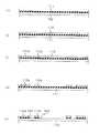
近年、電子機器の小型化に伴い、電子機器に搭載される半導体装置の小型化が要求されている。一例を挙げると、限られた実装領域で記憶容量を増やすために、複数の半導体素子(メモリ)を備えた半導体装置が求められている。この従来例に係る半導体装置について、図10を参照しながら説明する。図10は、従来例に係る半導体装置の断面図である。
【0003】
図10に示される半導体装置101は、配線基板109上に半導体素子106をフリップチップ接続して成る半導体装置108を上下に2つ積層した構造を有している。配線基板109は、ポリイミドフィルム102と配線パターン103とから成る。このうち、ポリイミドフィルム102には、スルーホール102a、102a、・・・が開口されている。そして、107、107、・・・は、はんだバンプであり、それらはスルーホール102a、102a、・・・を介して上記の配線パターン103と電気的に接続されている。なお、配線パターン103は、銅より成るものである。
【0004】
また、半導体素子106に着目すると、その電極端子形成面上には、金より成るスタッドバンプ105、105、・・・が形成されている。このスタッドバンプ105、105、・・・は半導体素子106の電極端子であり、それらは異方性導電膜104を介して配線パターン103と電気的に接続されている。
図示の如く、下側の半導体装置108の配線パターン103上に、上側の半導体装置108のはんだバンプ107、107、・・・が接合されており、それにより上下の半導体装置108同士が電気的かつ機械的に接続されている。そして、下側の半導体装置108のはんだバンプ107、107、・・・が実装基板110に当接した状態で該はんだバンプ107、107、・・・をリフローすることにより、半導体装置101と実装基板110とが電気的かつ機械的に接続される。また、下側及び上側の半導体装置108の厚みは約300μmであり、半導体装置101の全体の厚みは約600μmである。
【0005】
この半導体装置101によれば、その厚み方向に半導体素子106を2個備えているので、2つの半導体素子106を一平面内に配列する場合よりも実装面積を小さくすることができる。
次に、図11乃至図13を参照しながら、この従来例に係る半導体装置101の製造方法について説明する。図11乃至図13は、従来例に係る半導体装置の製造方法について示す断面図である。
【0006】
まず最初に、上側の半導体装置108を製造するために、図11(a)に示すように、銅箔111が接着された長尺状のポリイミドフィルム102を用意する。
次に、図11(b)に示すように、銅箔111上にフォトレジスト112を塗布する。
【0007】
次いで、図11(c)に示すように、フォトレジスト112に配線パターンを露光する。図中、112aは、この露光により感光したフォトレジストを示す。
続いて、図11(d)に示すように、フォトレジスト112を現像する。これにより、感光したフォトレジスト112aのみが銅箔111上に残り、配線とならない部分にある銅箔111の表面が露出する。
【0008】
次に、図11(e)に示すように、表面が露出している部分の銅箔111をエッチングする。この工程により、配線とならない部分にある銅箔111が除去され、配線パターン103(図10参照)がポリイミドフィルム102上に形成される。
次いで、図12(a)に示すように、配線パターン103を鉛直下方に向け、感光したフォトレジスト112aを除去する。
【0009】
続いて、図12(b)に示すように、ポリイミドフィルム102にレーザを照射し、スルーホール102a、102a、・・・(図10参照)を開口する。ここまでの工程により、ポリイミドフィルム102と配線パターン103とで構成される配線基板109が完成する。
次に、図12(c)に示すように、配線パターン103を再び鉛直上方に向ける。
【0010】
次いで、図12(d)に示すように、配線パターン103上に、フィルム状の異方性導電膜104を貼り付ける。
続いて、図12(e)に示すように、異方性導電膜104上に、半導体素子106を搭載する。この段階では、半導体素子106は、極弱い力で異方性導電膜104上に載せられており、半導体素子106と配線基板109との間にはまだ十分な接着力が得られていない。そして、スタッドバンプ105、105、・・・と配線パターン103との間にも、電気的な接続がまだ十分に得られていない。
【0011】
続いて、図13(a)に示すように、ステージ113上に配線基板109を載せ、ツール114を半導体素子106に押し当てると共に、異方性導電膜104を加熱する。これにより、異方性導電膜104が加熱・加圧されて硬化し、配線基板109と半導体素子106との間に十分な接着力が得られるようになる。また、加圧により、スタッドバンプ105、105、・・・と配線パターン103とで挟まれた部分にある異方性導電膜104が導電性を帯び、半導体素子106と配線基板とが電気的に接続されるようになる。以下では、異方性導電膜をこのように加熱・加圧する工程を、本圧着工程と称することにする。
【0012】
この本圧着工程が終了すると、図13(b)に示される工程が次に行われる。この工程では、スルーホール102a、102a、・・・から露出する配線パターン103上に、はんだバンプ107、107、・・・を搭載する。
以上の図においては、一つの半導体装置108に対応する部分が拡大されて示されているが、実際には、図13(c)に示すように、長尺状のポリイミドフィルム102上に複数の半導体装置108が形成される。
【0013】
その後、図13(d)に示すように、ポリイミドフィルム102を切断し、上記複数の半導体装置108を個片化する。
そして最後に、個片化した半導体装置108の各々について、その電気的特性が予め定められたスペックを満たしているかどうかを検査する。
以上により、図10に示される上側の半導体装置108が完成する。
【0014】
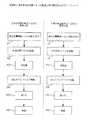
以上の製造工程の要点をまとめると、図14のようになる。図14は、従来例に係る半導体装置の製造方法の要点を示すフローチャートである。
図14の左側に示されるように、上記した上側の半導体装置108の製造工程は、要約すると次の6工程から成る。
工程P1:異方性導電膜104の貼り付け(図12(d)の工程)
工程P2:半導体素子106搭載(図12(e)の工程)
工程P3:本圧着(図13(a)の工程)
工程P4:はんだバンプ107搭載(図13(b)の工程)
工程P5:個片化(図13(d)の工程)
工程P6:検査
また、下側の半導体装置108(図10)参照についても、図14の右側に示されるように、上記した上側の半導体装置108の製造工程と同様の6工程を経て製造される。そして、下側の半導体装置108が完成すると、既に完成している上側半導体装置108と積層し、図10に示される半導体装置101が完成する。
【0015】
【発明が解決しようとする課題】
ところで、電子機器の小型化を更に進めるには、それに搭載される半導体装置の厚みはできるだけ薄いのが好ましい。
しかしながら、図10に示されるように、従来例に係る半導体装置101では厚み方向に配線基板109を2つも備えているので、この配線基板109の厚みの分だけ半導体装置101の厚みが厚くなってしまう。
【0016】
また、ポリイミド樹脂を主体に構成される配線基板109と、シリコンを主体に構成される半導体素子106のそれぞれの熱膨張率を比較すると、配線基板109の熱膨張率の方がはるかに大きい。そのため、はんだバンプ107、107、・・・をリフローする場合のように、半導体装置101が加熱される状況において、配線基板109と半導体素子106との熱膨張率の差により配線基板109に応力が生じ、該配線基板109に反りが生じてしまう。
【0017】
しかしながら、配線基板109にこのように反りが生じると、スタッドバンプ105、105、・・・が異方性導電膜104から剥離し、半導体素子106と配線基板109との電気的な接続信頼性が低下してしまう。
一方、半導体装置の製造方法については、半導体装置の製造コストを低減するために、工程数ができるだけ少ないのが望ましい。
【0018】
しかしながら、図14に示されるように、従来では、上側の半導体装置108と下側の半導体装置108の各々が全く同じ工程を経て製造されるので、一つの半導体装置101を製造するのに同じ工程を2回行わなければならず、工程数が多くなってしまう。具体的には、図14に示される工程P1乃至工程P6の6工程を上側及び下側の半導体装置108の各々について行わなければならず、全部で12工程(=6工程×2)もの工程が必要となってしまう。
【0019】
本発明は係る従来例の問題点に鑑みて創作されたものであり、従来よりも厚みが薄く、且つ半導体素子と配線基板との電気的な接続信頼性が向上された半導体装置、及び、それを従来よりも少ない工程数で製造することができる製造方法を提供することを目的とするものである。
【0020】
【課題を解決するための手段】
上記した課題は、第1の発明である、貫通孔が形成された絶縁性の樹脂フィルムと、前記樹脂フィルムの一方の面に形成され、第1の半導体素子用パッドと、少なくとも該一方の面における前記貫通孔の開口部を覆う第2の半導体素子用パッドとを有する配線パターンと、前記配線パターンの前記第1の半導体素子用パッドと電気的に接続するように、該配線パターン上にフリップチップ接続された第1の半導体素子と、前記貫通孔を介して前記配線パターンの前記第2の半導体素子用パッドと電気的に接続するように、前記樹脂フィルムの他方の面側にフリップチップ接続された第2の半導体素子と、前記配線パターンと電気的に接続された外部接続端子とを備え、前記第1の半導体素子と前記第2の半導体素子とが完全には重ならないように互いにずらして配置されると共に、前記第1の半導体素子用パッドと前記第2の半導体素子用パッドとが短絡しないように離間して配置されたことを特徴とする半導体装置によって解決する。
【0021】
又は、第2の発明である、前記第1の半導体素子は前記第2の半導体素子に対して第1の方向にずらして配置され、前記第1及び第2の半導体素子用パッドはそれぞれ少なくとも2つ設けられ、前記第1の半導体素子と前記第2の半導体素子とが重なる領域の中心を前記第1の方向と垂直な方向に横切る中心線の前記第1の方向の側では、前記第1の半導体素子用パッドの一方は前記第2の半導体素子用パッドの一方よりも外側に配置され、前記中心線の前記第1の方向と反対の第2の方向の側では、前記第1の半導体素子用パッドの他方は前記第2の半導体素子用パッドの他方よりも内側に配置されたことを特徴とする第1の発明に記載の半導体装置によって解決する。
又は、第3の発明である、前記樹脂フィルムの前記第1の半導体素子が接続された前記一方の面と反対の前記他方の面の前記第1の半導体素子と前記第2の半導体素子とが重ならない領域、及び、前記樹脂フィルムの前記第2の半導体素子が接続された前記他方の面と反対の前記一方の面の前記第1の半導体素子と前記第2の半導体素子とが重ならない領域のうちの少なくとも一方に、ダミー半導体チップが固着されたことを特徴とする第1の発明に記載の半導体装置によって解決する。
又は、第4の発明である、前記第1の半導体素子及び前記第2の半導体素子として、同一機能及び同一の電極端子配列を有するものを用いることを特徴とする第1の発明乃至第3の発明のいずれか一の発明に記載の半導体装置によって解決する。
【0022】
又は、第5の発明である、前記樹脂フィルムのいずれか一方の面の周縁領域に、補強板が固着されたことを特徴とする第1の発明乃至第4の発明のいずれか一の発明に記載の半導体装置によって解決する。
又は、第6の発明である、絶縁性の樹脂フィルムの一方の面に、第1の半導体素子用パッドと、前記第1の半導体素子用パッドと短絡しないように離間して配置された第2の半導体素子用パッドを有する配線パターンを形成する工程と、前記樹脂フィルムに、開口部が前記配線パターンの前記第2の半導体素子用パッドにより覆われた貫通孔を形成する工程と、前記配線パターン上に第1の異方性導電膜を形成する工程と、前記配線パターンを形成した後に、前記樹脂フィルムの他方の面及び前記貫通孔の内部に第2の異方性導電膜を形成する工程と、突起状の電極端子を備えた第1の半導体素子の一方の面を、前記第1の異方性導電膜上に仮圧着する工程と、突起状の電極端子を備えた第2の半導体素子の一方の面を、該電極端子が前記第2の異方性導電膜を介して前記貫通孔に挿入されるように、前記第2の異方性導電膜上に仮圧着して、前記第1の半導体素子と前記第2の半導体素子とを完全には重ねないように互いにずらして配置する工程と、前記第1の異方性導電膜及び前記第2の異方性導電膜が加熱された状態で、前記第1の半導体素子及び前記第2の半導体素子の他方の面を同時に加圧して、前記第1の半導体素子の前記電極端子と前記配線パターンの前記第1の半導体素子用パッドとを電気的に接続すると共に、前記第2の半導体素子の前記電極端子と前記配線パターンの前記第2の半導体素子用パッドとを電気的に接続する本圧着工程とを含むことを特徴とする半導体装置の製造方法によって解決する。
又は、第7の発明である、前記配線パターンを形成する工程では、前記第1及び第2の半導体素子用パッドをそれぞれ少なくとも2つ形成し、前記第2の半導体素子を前記第2の異方性導電膜上に仮圧着する工程では、前記第2の半導体素子を前記第1の半導体素子に対して第1の方向にずらして配置し、前記配線パターンを形成する工程では、前記第1の半導体素子と前記第2の半導体素子とが重なる領域の中心を、前記第1の方向と垂直な方向に横切る中心線の前記第1の方向の側では、前記第2の半導体素子用パッドの一方を前記第1の半導体素子用パッドの一方よりも外側に配置し、前記中心線の前記第1の方向と反対の第2の方向の側では、前記第2の半導体素子用パッドの他方を前記第1の半導体素子用パッドの他方よりも内側に配置することを特徴とする第6の発明に記載の半導体装置の製造方法によって解決する。
又は、第8の発明である、更に、ダミー半導体チップの一方の面を、前記第1の異方性導電膜上の前記第1の半導体素子と前記第2の半導体素子とが重ならない領域、及び、前記第2の異方性導電膜上の前記第1の半導体素子と前記第2の半導体素子とが重ならない領域のうちの少なくとも一方に仮圧着する工程を含み、前記本圧着工程では、前記第1の異方性導電膜及び前記第2の異方性導電膜が加熱された状態で、前記第1の半導体素子、前記第2の半導体素子及び前記ダミー半導体チップの他方の面を同時に加圧することを特徴とする第6の発明に記載の半導体装置の製造方法によって解決する。
【0023】
次に、本発明の作用について説明する。
本発明に係る半導体装置によれば、貫通孔の形成された絶縁性の樹脂フィルムを備えている。この樹脂フィルムの一方の面には、少なくとも該一方の面における上記開口部を覆う配線パターンが形成されている。そして、この配線パターン上には、該配線パターンと電気的に接続するように第1の半導体素子がフリップチップ接続されている。
【0024】
一方、上記樹脂フィルムの他方の面には、上記貫通孔を介して上記配線パターンと電気的に接続するように、第2の半導体素子がフリップチップ接続されている。そして、外部接続端子が上記の配線パターンに電気的に接続されている。
この構造によると、上記の樹脂フィルムと配線パターンとで配線基板が構成されるが、該配線基板は半導体装置の厚み方向に1つしか備えられていない。そのため、半導体装置の厚み方向に配線基板を2つ備える従来例と比較して、半導体装置の厚みが薄くされる。
【0025】
更に、上記の構造では、樹脂フィルムの両方の面側にそれぞれ第1の半導体素子と第2の半導体素子とを備えているので、樹脂フィルムと半導体素子の熱膨張率の差に起因して樹脂フィルムの両面に生じる応力が互いに相殺される。従って、半導体装置が加熱される状況下においても、従来のように配線基板に反りが生じることが無いので、上記半導体素子と配線基板との電気的な接続信頼性が向上される。
【0026】
なお、上記第1の半導体素子と上記第2の半導体装置とをそれらが完全には重ならないように互いにずらして配置しても良い。このようにすると、上記配線パターンにおいて、第1の半導体素子と電気的に接続される部分と、第2の半導体素子と電気的に接続される部分とが互いに離間して配置されるので、これらの部分が短絡しなくなる。
【0027】
そして、このように第1の半導体素子と第2の半導体素子とを互いにずらして配置する場合は、応力相殺板を設けても良い。この応力相殺板は、上記樹脂フィルムのいずれか一方の面側において、上記第1の半導体素子と上記第2の半導体素子とが重ならない領域に固着されるものである。この領域では、上記2つの半導体素子が重なっていないので、これらの半導体素子から樹脂フィルムに作用する応力が相殺されずに残っている。従って、この領域に応力相殺板を固着すると、この応力相殺板から樹脂フィルムに作用する応力と、相殺されずに残っている応力とが互いに相殺させられ、この領域における配線基板の反りが抑えられる。
【0028】
また、第1の半導体素子と第2の半導体素子として、同一機能及び同一の電極端子配列を有するものを用いると、上記配線パターンのデザインが簡略化される。これは、同一の電極端子配列を有するものを用いると、樹脂フィルム上に対称軸が存在するようになり、上記2つの半導体素子の同一の電極端子同士がこの対象軸に関して線対称の位置関係になるので、該同一の電極同士を直線的に接続することができるようになるからである。なお、このように同一の電極端子同士を接続することができるのは、上記2つの半導体素子として同一の機能を有するものを用いたためであることに注意されたい。
【0029】
更に、前記樹脂フィルムのいずれか一方の面の周縁領域に、補強板を固着しても良い。この補強板により、半導体装置の強度が高められる。
そして、本発明に係る半導体装置の製造方法によれば、上記第1の半導体装置と上記第2の半導体素子とが配線パターンに同時に電気的に接続される本圧着工程が含まれる。2つの半導体素子を配線パターンにこのように同時に電気的に接続することにより、半導体装置の製造工程数が削減されるので、該半導体装置の製造コストが安くされる。
【0030】
【発明の実施の形態】
(1)本発明の実施の形態に係る半導体装置についての説明
まず最初に、本実施形態に係る半導体装置について、図1乃至図4を参照しながら説明する。
図1は、本実施形態に係る半導体装置の断面図である。図1に示されるように、本実施形態に係る半導体装置201は、厚みが約20μmのポリイミドフィルム202(絶縁性の樹脂フィルム)を備えている。このポリイミドフィルム202は、その一方の面上に、厚みが約12μmの銅から成る配線パターン203が形成され、更に、はんだバンプ用スルーホール202b、202b、・・・が開口されている。これらポリイミドフィルム202と配線パターン203とにより、配線基板204が構成される。
【0031】
なお、ポリイミドフィルム202に代えて、ガラス・エポキシ樹脂やセラミック等から成るリジッドな基材を用いても良いが、半導体装置201の厚みを薄くするという観点からすると、本実施形態のようにポリイミドフィルム202を用いるのが好ましい。
また、ポリイミドフィルム202の他方の面上には、はんだバンプ205、205、・・・(外部接続端子)が接合されているが、このはんだバンプ205、205、・・・は、上記はんだバンプ用スルーホール202bを介して、はんだバンプ用電極パッド203cと電気的に接続されている。このはんだバンプ205、205、・・・が実装基板(図示せず)に当接した状態で該はんだバンプ205、205、・・・をリフローすることにより、半導体装置201が実装基板上に電気的かつ機械的に接続される。
【0032】
そして、図示の如く、配線基板204の両面には、第1の半導体素子206と第2の半導体素子209とがフリップチップ接続されている。これら第1の半導体素子206と第2の半導体素子209の厚みは、いずれも約50μmである。
ここで、第1の半導体素子206の接続形態を見るために、図1の点線円内を参照する。これに示されるように、第1の半導体素子206は、金より成るスタッドバンプ(突起状の電極端子)207をその電極端子形成面上に備えている。このスタッドバンプ207の高さは約30μmである。そして、203aは、第1の半導体素子用電極パッドであり、これは、配線パターン203においてスタッドバンプ207に対応する位置に形成されるものである。
【0033】
また、第1の半導体素子206と配線基板204との間には、第1の異方性導電膜208が形成されている。この第1の異方性導電膜208は、スタッドバンプ207の先端部と第1の半導体素子用電極パッド203aとで挟まれた部分においてのみ、厚み方向に導電性を帯びている。そして、この導電性を帯びた部分を介して、スタッドバンプ207と第1の半導体素子用電極パッド203aとが電気的に接続されれている。このように、第1の半導体素子206と配線パターン203とは、第1の異方性導電膜208を介して電気的に接続されている。
【0034】
引き続き図1の点線円内を参照し、今度は第2の半導体素子209の接続形態に着目する。この第2の半導体素子209は、金より成るスタッドバンプ(突起状の電極端子)211をその電極端子形成面に備えている。このスタッドバンプ211の高さは約30μmである。そして、ポリイミドフィルム202において、このスタッドバンプ211に対応する位置には、スタッドバンプ用スルーホール202a(貫通孔)が開口されている。
【0035】
ポリイミドフィルム202の一方の面上には、上記のように配線パターン203が形成されているが、該配線パターン203には更に第2の半導体素子用電極パッド203bが形成されている。図示の如く、この第2の半導体素子用電極パッド203bは、スタッドバンプ用スルーホール202aの開口部を覆うようにして形成されている。換言すると、配線パターン203は、スタッドバンプ用スルーホール202aの開口部を覆うようにして形成されている。
【0036】
スタッドバンプ用スルーホール202aは、その内部が第2の異方性導電膜210で満たされていると共に、スタッドバンプ211が挿入されている。この第2の異方性導電膜210は、スタッドバンプ211の先端部と第2の半導体素子用電極パッド203bとで挟まれた部分においてのみ、厚み方向に導電性を帯びている。そして、この導電性を帯びた部分により、スタッドバンプ211と第2の異方性導電膜210とが電気的に接続されている。このように、第2の半導体素子209と配線パターン203とは、スタッドバンプ用スルーホール202aを介して電気的に接続されている。
【0037】
上のようにして成る半導体装置201によると、2つの半導体素子(第1の半導体素子206、第2の半導体素子209)をその厚み方向に備えているので、該2つの半導体素子を一平面内に配列する場合よりも実装面積を小さくすることができる。
これに加えて、半導体装置201は配線基板204を厚み方向に1つしか備えていないため、配線基板109を厚み方向に2つ備える従来例(図10参照)と比較してその厚みを薄くすることができる。具体的には、半導体装置201の厚みは約300μmであり、これは従来例に係る半導体装置101の厚み(約600μm)よりも格段に薄い値である。このことは、近年求められている電子機器の小型化に大きく寄与する。
【0038】
また、従来の技術の項で説明したように、ポリイミドとシリコンのそれぞれの熱膨張率が大きく異なるため、従来では半導体装置108(図10参照)が加熱される状況下において配線基板109(図10参照)に反りが生じていた。
これに対し、半導体装置201の構造によれば、ポリイミドフィルム202の両方の面側にそれぞれ第1の半導体素子206と第2の半導体素子209とを備えている。そのため、第1の半導体素子206からポリイミドフィルム202の一方の面(配線パターン203の形成面)に作用する応力と、第2の半導体素子209からポリイミドフィルム202の他方の面に作用する応力とが互いに相殺される。
【0039】
従って、はんだバンプ205、205、・・・をリフローする場合のように半導体装置201が加熱される状況下であっても、従来のように配線基板204が応力により反ることが無い。これにより、スタッドバンプ(207、211)が異方性導電膜(208、210)から剥離することが無くなり、配線パターン203と半導体素子(206、209)との間の電気的な接続信頼性を向上させることができる。
【0040】
また、図1に示されるように、第1の半導体素子206と第2の半導体素子209とは、厚み方向から見た場合に完全には重ならないように配置されている。このように配置すると、第1の半導体素子用電極パッド203aと第2の半導体素子用電極パッド203bとをそれらが短絡しないように互いに離間して配置することができる。これができるために、本実施形態においては、点線円内に示されるように、第1の半導体素子206の側壁206aと、第2の半導体素子209の側壁209aとを、紙面の左右方向に約1.2mm程ずらしてある。
【0041】
なお、このように第1の半導体素子206と第2の半導体素子209とをずらして配置する場合、これらの半導体素子が重ならないで互いにずれている領域では、ポリイミドフィルム202に作用する応力が上のように相殺されずに残ることが考えられる。これは、この領域では、ポリイミドフィルム202の片方の面側にしか半導体素子が固着されていないので、この半導体素子から上記片方の面に作用する応力を相殺するような応力が存在しないためである。
【0042】
この点が懸念される場合は、図2に示されるようなダミーチップ212(応力相殺板)を用いるのが良い。このダミーチップ212は、ポリイミドフィルム202の2つの面のうち配線パターン203が形成されてない方の面上に、第2の異方性導電膜210を介して固着されている。そして、図示の如く、このダミーチップ212が固着されている領域は、第1の半導体素子206と第2の半導体素子209とがずれている領域であり、第1の半導体素子206からポリイミドフィルム202に作用する応力が相殺されずに残っている領域である。
【0043】
この領域にダミーチップ212を配置すると、該ダミーチップ212からポリイミドフィルム202に作用する応力と、該領域に相殺されずに残っている応力とを互いに相殺させることができる。
これにより、たとえ第1の半導体素子206と第2の半導体素子209とを互いにずらして配置しても、それに伴ってポリイミドフィルム202上に残る応力を相殺し、半導体装置201の反りを抑えることができるようになる。
【0044】
なお、このダミーチップ212としては、回路が形成されていないシリコンチップ等が用いられる。また、図2においては、ポリイミドフィルム202の2つの面のうち、配線パターン203が形成されてない方の面上にダミーチップ212が固着されているが、配線パターン203が形成されている面上にダミーチップ212を固着しても、上記したのと同様の作用、効果が奏される。
【0045】
ところで、上においては、第1の半導体素子206と第2の半導体素子209の種類について特に言及しなかったが、これらの半導体素子(206、209)として同一機能、及び同一の電極端子(スタッドバンプ)配列を有するものを用いると、配線パターン203のデザインを簡略化することができる。これについて、図3を参照しながら説明する。図3は、ポリイミドフィルム202とそれに形成された配線パターン203とを、第1の半導体素子206側から見た場合の平面図である。
【0046】
図3において、小文字のアルファベットa、b、c、d、e、f、g、h、iは、第1の半導体素子用電極パッド203aの一つ一つを表す記号である。そして、大文字のアルファベットA、B、C、D、E、F、G、H、Iは、第2の半導体素子用電極パッド203bの一つ一つを表す記号である。
上記したように、第1の半導体素子206と第2の半導体素子209とは同一の電極端子配列を有しているで、同じアルファベット(aとA、bとB、・・・、hとH)で表される電極パッドには、2つの半導体素子(206、209)の同じスタッドバンプ(図1の207、211を参照)が電気的に接続されることになる。そして、2つの半導体素子(206、209)は同一の機能を有しているので、上記同じアルファベット(aとA、bとB、・・・、hとH)で表される電極パッド同士は、配線パターン203により電気的に接続し、共通のはんだバンプ205(図1参照)により外部に引き出して構わない。
【0047】
特に、記号F、G、H、Iで表されるパッド群と、記号f、g、h、iで表されるパッド群に着目すると、それらは直線状の簡単な配線パターン203により電気的に接続されている。このように配線パターン203を直線状にできるのは、図中の対称軸に関して上記2群のパッド群が線対称の関係にあるからである。そして、このような対称軸が存在するのは、2つの半導体素子(206、209)として同一の電極端子配列を有するものを用いたためであることに注意されたい。
【0048】
このように、2つの半導体素子(206、209)として同一機能、及び同一の電極端子配列を有するものを用いると、配線パターン203のデザインを簡略化することができる。
なお、図3の点線円内に示されるものは、配線パターン203の拡大図である。これに示されるように、本実施形態においては、配線幅は約50μmであり、そして配線間隔も50μmである。
【0049】
更に、図4に示すように、半導体装置201の強度を高めるために、ポリイミドフィルム202の面の周縁領域に、補強板213を固着しても良い。図4は、補強板213を固着した場合の半導体装置201の斜視図である。
図4においては、ポリイミドフィルム202の2つの面のうち、第1の半導体素子206側の面上に補強板213が固着されているが、第2の半導体素子209側(図1参照)の面上に補強板213を固着しても、半導体装置201の強度を高めることができる。そして、この補強板213としては、例えば、ステンレス板、銅板、CFRP(Carbon Fiber Reinforced Plastic)板等が用いられ、これらは接着剤(図示せず)によりポリイミドフィルム202上に接着される。
【0050】
なお、本実施形態においては、半導体素子(206、209)が異方性導電膜(208、210)を介して配線基板204にフリップチップ接続されているが、本発明におけるフリップチップ接続はこれに限られるものではない。例えば、CCB(Controlled Collapse Bonding Connection)実装、ESC(Epoxy Solder Encapslated Connection)実装、SBB(Stud Bump Bonding)実装、BIT(Bump Interconnection technology )実装等を用いたフリップチップ接続でも、上記したのと同様の作用、効果が奏される。
【0051】
(2)本発明の実施の形態に係る半導体装置の製造方法についての説明
次に、上記した半導体装置201の製造方法について、図5乃至図9を参照しながら説明する。図5乃至図8は、本実施形態に係る半導体装置の製造方法について示す断面図である。そして、図9は、本実施形態に係る半導体装置の製造方法の要点を示すフローチャートである。
【0052】
まず最初に、図5(a)に示すように、一方の面に銅箔214が接着された長尺状のポリイミドフィルム202(絶縁性の樹脂フィルム)を用意する。後述するように、銅箔214は、後でパターニングされて配線パターン203(図1参照)となるものである。このポリイミドフィルム202の厚みは20μmであり、銅箔214の厚みは12μmである。
【0053】
次に、図5(b)に示すように、銅箔214上にフォトレジスト215を塗布する。
続いて、図5(c)に示すように、フォトレジスト215に配線パターンを露光する。図中、215aは、露光により感光したフォトレジストを示し、そのパターンは配線パターン203(図1参照)と同様である。
【0054】
次いで、図5(d)に示すように、フォトレジスト215を現像する。この現像により、上記の露光で感光しなかった部分のフォトレジスト215が除去される。これにより、感光したフォトレジスト215aのみが銅箔214上に残り、銅箔214において配線とならない部分の表面が露出する。
次に、図5(e)に示すように、感光したフォトレジスト215aをマスクにして、銅箔214をウエットエッチングする。このウエットエッチングにより、第1の半導体素子用電極パッド203a、第2の半導体素子用電極パッド203b、及びはんだバンプ用電極パッド203c等から成る配線パターン203が、ポリイミドフィルム202の一方の面に形成される。
【0055】
続いて、図6(a)に示すように、感光したフォトレジスト215aを除去する。
次いで、図6(b)に示すように、ポリイミドフィルム202の2つの面のうち、配線パターン203が形成されている方の面を鉛直下向きに向ける。
次に、図6(c)に示すように、ポリイミドフィルム202にレーザを照射し、はんだバンプ用スルーホール202b、202b、・・・とスタッドバンプ用スルーホール(貫通孔)202a、202a、・・・とを開口する。この際に用いるレーザとしては、例えばエキシマレーザ、YAGレーザ、CO2レーザ等がある。
【0056】
同図に示されるように、スタッドバンプ用スルーホール202a、202a、・・・の開口部は、配線パターン203の一部である第2の半導体素子用電極パッド203bにより覆われている。ここまでの工程により、配線基板204が作製されたことになる。
続いて、図6(d)に示すように、ポリイミドフィルム202の2つの面のうち、配線パターン203が形成されていない方の面上に、フィルム状の第2の異方性導電膜210を接着する。この接着では、ポリイミドフィルム202の面上だけでなく、スタッドバンプ用スルーホール202a、202a、・・・の内部にも第2の異方性導電膜210が形成される。
【0057】
次いで、図6(e)に示すように、ポリイミドフィルム202の2つの面のうち、配線パターン203が形成されている方の面を鉛直上向きに向ける。そして、この配線パターン203上にフィルム状の異方性導電膜を接着することにより、第1の異方性導電膜208を形成する。
次に、図7(a)に示すように、第1の半導体素子206の電極端子形成面を第1の異方性導電膜208上に仮圧着する。ここで、仮圧着とは、第1の半導体素子206を鉛直下向きに向けても(すなわち、図に示される構造を上下に反転しても)、重力により第1の半導体素子206が第1の異方性導電膜208から剥離してしまわない程度に圧着することを意味する。
【0058】
この仮圧着により、スタッドバンプ207(突起状の電極端子)が第1の異方性導電膜208中に埋め込まれ、該スタッドバンプ207の先端部が第1の半導体素子用電極パッド203aの表面に近接するようになるが、該先端部と該表面とが接することはなく、それらは第1の異方性導電膜208により隔てられている(同図の点線円内を参照)。また、この仮圧着の段階では、第1の異方性導電膜208はまだ導電性を帯びておらず、スタッドバンプ207と第1の半導体素子用電極パッド203aとは電気的に接続されていない。
【0059】
続いて、図7(b)に示すように、第1の半導体素子206を鉛直下向きに向けた状態で、第2の半導体素子209の電極端子形成面を第2の異方性導電膜210上に仮圧着する。
この仮圧着では、第2の異方性導電膜210を介して、スタッドバンプ211(突起状の電極端子)がスタッドバンプ用スルーホール202aに挿入される。同図の点線円内に示されるように、この仮圧着により、スタッドバンプ211の先端部が第2の半導体素子用電極パッド203bの表面に近接するようになる。しかし、これら先端部と表面とが接することはなく、それらは第2の異方性導電膜210により隔てられている。
【0060】
また、この仮圧着の段階では、第2の異方性導電膜210はまだ導電性を帯びておらず、スタッドバンプ207と第2の半導体素子用電極パッド203bとは電気的に接続されていない。
次いで、上の仮圧着が終了すると、図7(c)に示される本圧着工程が行われる。この本圧着工程においては、まず、ステージ216上に、第1の半導体素子206の電極端子形成面の反対面を載せる。そして、第1の異方性導電膜208及び第2の異方性導電膜210の各々が加熱された状態で、第2の半導体素子209の電極端子形成面の反対面をツール217で加圧する。このようにすると、第1の半導体素子206の電極端子形成面の反対面も、ステージ216により加圧されるようになる。
【0061】
第1の半導体素子206と第2の半導体素子209を上のように加圧すると、これらの半導体素子とポリイミドフィルム202とで挟まれた第1の異方性導電膜208及び第2の異方性導電膜210が、加熱下において加圧されることになる。
このように加熱・加圧すると、第1の異方性導電膜208において、スタッドバンプ207の先端部と第1の半導体素子用電極パッド203aとの間にある部分(図7(a)の点線円内を参照)が、厚み方向に導電性を帯びるようになる。同様に、第2の異方性導電膜210も、スタッドバンプ211の先端部と第2の半導体素子用電極パッド203bとの間にある部分(図7(b)の点線円内を参照)が、厚み方向に導電性を帯びるようになる。
【0062】
これにより、スタッドバンプ207及びスタッドバンプ211が、それぞれ第1の半導体素子用電極パッド203a及び第2の半導体素子用電極パッド203bに電気的に接続されることになる。
更に、この加熱・加圧により、第1の異方性導電膜208と第2の異方性導電膜210とが硬化し、第1の半導体素子206と第2の半導体素子209とがこれらの異方性導電膜を介して十分な接着力で配線基板204に接着される。
【0063】
このように、この本圧着工程では、2つの半導体素子(206、209)が配線基板204に同時に搭載することができる。そのため、2つの半導体素子を別々に搭載していた従来例と比較して工程数が減らせ、半導体装置201の製造コストを安くすることができるようになる。
この本圧着工程が終了すると、次に図7(d)に示される工程が行われる。この工程では、はんだバンプ205がはんだバンプ用電極パッド203c上に搭載される。
【0064】
以上の図においては、一つの半導体装置201に対応する部分が拡大されて示されているが、実際には、図8(a)に示すように、長尺状のポリイミドフィルム202上に複数の半導体装置201が形成される。
その後、図8(b)に示すように、ポリイミドフィルム202を切断し、上記複数の半導体装置210を個片化する。
【0065】
この後は、個片化された半導体装置201の各々について、その電気的特性が予め定められたスペックを満たしているかどうかが検査される。
以上により、本実施形態に係る半導体装置201が完成する。以上の製造工程の要点をまとめると、図9のようになる。
図9に示されるように、半導体装置201の製造工程は、要約すると次の8工程から成る。
【0066】
工程S1:第2の異方性導電膜210の形成(図6(d)の工程)
工程S2:第1の異方性導電膜208の形成(図6(e)の工程)
工程S3:第1の半導体素子206の仮圧着(図7(a)の工程)
工程S4:第2の半導体素子209の仮圧着(図7(b)の工程)
工程S5:第1の半導体素子206及び第2の半導体素子209の本圧着(図7(c)の工程)
工程S6:はんだバンプ205搭載(図7(d)の工程)
工程S7:個片化(図8(b)の工程)
工程S8:検査
従来例に係る半導体装置の製造方法では、図14に示して説明したように、半導体装置101が完成するまでに全部で12工程が必要であった。これに対し、本実施形態に係る半導体装置の製造方法では、従来よりも少ない8工程で半導体装置201を完成させることができる。特に、工程S5(本圧着工程)においては、2つの半導体素子(206、209)の本圧着が1工程で済まされており、工程数の大幅な削減が図られている。これにより、本実施形態に係る半導体装置の製造方法では、従来よりも安い製造コストで半導体装置201を製造することができる。
【0067】
【発明の効果】
以上説明したように、本発明に係る半導体装置によると、樹脂フィルムと配線パターンとで構成される配線基板を厚み方向に1つしか備えていないので、厚み方向に配線基板を2つ備える従来例と比較して、その厚みを薄くすることができる。
【0068】
また、この半導体装置は、樹脂フィルムの両方の面側にそれぞれ第1の半導体素子と第2の半導体素子とを備えているので、樹脂フィルムの両面に作用する応力が互いに相殺され、配線基板の反りを抑えることができる。これにより、半導体素子の電極端子が従来のように異方性導電膜から剥離することが無くなるので、半導体素子と配線基板との電気的な接続信頼性を向上させることができる。
【0069】
更に、第1の半導体素子と第2の半導体素子とをそれらが完全には重ならないように配置すると、配線パターンにおいて、第1の半導体素子と電気的に接続される部分と、第2の半導体素子と電気的に接続される部分とを互いに離間して配置することができ、これらの部分が短絡しないようにすることができる。
そして、このように第1の半導体素子と第2の半導体素子とをずらして配置する場合は、樹脂フィルムのいずれか一方の面側において、上記第1の半導体素子と第2の半導体素子とが重ならない領域に応力相殺板を固着することにより、上記領域における配線基板の反りが抑えられる。
【0070】
また、上記第1の半導体素子と第2の半導体素子として、同一機能及び同一の電極端子配列を有するものを用いると、上記配線パターンのデザインを簡略化することができる。
更にまた、樹脂フィルムのいずれか一方の面の周縁領域に補強板を固着することにより、半導体装置の強度が高められる。
【0071】
そして、本発明に係る半導体装置の製造方法によると、本圧着工程において上記第1の半導体装置と上記第2の半導体素子とが配線パターンに同時に電気的に接続されるので、半導体装置の製造工程数の削減が図られ、該半導体装置の製造工程を安くすることができる。
【図面の簡単な説明】
【図1】本発明の実施の形態に係る半導体装置の断面図である。
【図2】応力相殺板を設けた場合の本発明の実施の形態に係る半導体装置の断面図である。
【図3】本発明の実施の形態に係る半導体装置の配線パターンの平面図である。
【図4】補強板を設けた場合の本発明の実施の形態に係る半導体装置の斜視図である。
【図5】本発明の実施の形態に係る半導体装置の製造方法について示す断面図(その1)である。
【図6】本発明の実施の形態に係る半導体装置の製造方法について示す断面図(その2)である。
【図7】本発明の実施の形態に係る半導体装置の製造方法について示す断面図(その3)である。
【図8】本発明の実施の形態に係る半導体装置の製造方法について示す断面図(その4)である。
【図9】本発明の実施の形態に係る半導体装置の製造方法の要点を示す断面図である。
【図10】従来例に係る半導体装置の断面図である。
【図11】従来例に係る半導体装置の製造方法について示す断面図(その1)である。
【図12】従来例に係る半導体装置の製造方法について示す断面図(その2)である。
【図13】従来例に係る半導体装置の製造方法について示す断面図(その3)である。
【図14】従来例に係る半導体装置の製造方法の要点を示すフローチャートである。
【符号の説明】
101、201・・・半導体装置、
102、202・・・ポリイミドフィルム、
102a・・・スルーホール、
103、203・・・配線パターン、
104・・・異方性導電膜、
105、207、211・・・スタッドバンプ、
106・・・半導体素子、
107、205・・・はんだバンプ、
108・・・半導体装置、
109、204・・・配線基板
110・・・実装基板、
111、214・・・銅箔、
112、215・・・フォトレジスト、
112a、215a・・・感光したフォトレジスト、
113、216・・・ステージ、
114、217・・・ツール、
202a・・・スタッドバンプ用スルーホール、
202b・・・はんだバンプ用スルーホール、
203a・・・第1の半導体素子用電極パッド、
203b・・・第2の半導体素子用電極パッド、
203c・・・はんだバンプ用電極パッド、
206・・・第1の半導体素子、
208・・・第1の異方性導電膜、
209・・・第2の半導体素子、
210・・・第2の異方性導電膜、
212・・・ダミーチップ、
213・・・補強板。[0001]
BACKGROUND OF THE INVENTION
The present invention relates to a semiconductor device including a plurality of semiconductor elements and a method for manufacturing the same. More specifically, the present invention relates to a technique useful for reducing the size of a semiconductor device including a plurality of semiconductor elements and reducing the cost of a method for manufacturing the semiconductor device.
[0002]
[Prior art]
In recent years, with the miniaturization of electronic devices, there has been a demand for miniaturization of semiconductor devices mounted on electronic devices. For example, in order to increase the storage capacity in a limited mounting area, a semiconductor device including a plurality of semiconductor elements (memory) is required. A semiconductor device according to this conventional example will be described with reference to FIG. FIG. 10 is a cross-sectional view of a conventional semiconductor device.
[0003]
A
[0004]
Focusing on the
As shown in the figure,
[0005]
According to the
Next, a method for manufacturing the
[0006]
First, in order to manufacture the
Next, as shown in FIG. 11B, a
[0007]
Next, as shown in FIG. 11C, the
Subsequently, as shown in FIG. 11D, the
[0008]
Next, as shown in FIG. 11E, the
Next, as shown in FIG. 12A, the
[0009]
Then, as shown in FIG.12 (b), a laser is irradiated to the
Next, as shown in FIG. 12C, the
[0010]
Next, as illustrated in FIG. 12D, a film-like anisotropic
Subsequently, as illustrated in FIG. 12E, the
[0011]
Subsequently, as illustrated in FIG. 13A, the
[0012]
When this main press-bonding step is completed, the step shown in FIG. 13B is performed next. In this step, solder bumps 107, 107,... Are mounted on the
In the above drawings, a portion corresponding to one
[0013]
Thereafter, as shown in FIG. 13D, the
Finally, each of the separated
Thus, the
[0014]
The main points of the above manufacturing process are summarized as shown in FIG. FIG. 14 is a flowchart showing the main points of a conventional method for manufacturing a semiconductor device.
As shown on the left side of FIG. 14, the manufacturing process of the
Step P1: Application of anisotropic conductive film 104 (step of FIG. 12D)
Step P2: mounting of the semiconductor element 106 (step of FIG. 12E)
Process P3: final pressure bonding (process of FIG. 13A)
Step P4: mounting of solder bumps 107 (step of FIG. 13B)
Step P5: Individualization (step of FIG. 13 (d))
Process P6: Inspection
Also, referring to the lower semiconductor device 108 (FIG. 10), as shown on the right side of FIG. 14, the
[0015]
[Problems to be solved by the invention]
By the way, in order to further reduce the size of the electronic device, it is preferable that the thickness of the semiconductor device mounted thereon is as thin as possible.
However, as shown in FIG. 10, the
[0016]
Further, comparing the thermal expansion coefficients of the
[0017]
However, when the
On the other hand, regarding the method for manufacturing a semiconductor device, it is desirable that the number of processes is as small as possible in order to reduce the manufacturing cost of the semiconductor device.
[0018]
However, as shown in FIG. 14, conventionally, each of the
[0019]
The present invention has been created in view of the problems of the related art, and a semiconductor device having a smaller thickness than the conventional one and improved electrical connection reliability between the semiconductor element and the wiring board, and the semiconductor device It is an object of the present invention to provide a production method capable of producing the process with fewer steps than in the past.
[0020]
[Means for Solving the Problems]
The above-described problem is the first invention, an insulating resin film having a through-hole formed thereon, and is formed on one surface of the resin film,A first semiconductor element pad;Cover the opening of the through hole on at least one of the surfacesAnd a second semiconductor element pad.Wiring pattern and said wiring patternThe first semiconductor element padA first semiconductor element flip-chip connected on the wiring pattern so as to be electrically connected to the wiring pattern, and the wiring pattern via the through holeThe second semiconductor element padA second semiconductor element flip-chip connected to the other surface of the resin film so as to be electrically connected to the wiring pattern, and an external connection terminal electrically connected to the wiring pattern.The first semiconductor element and the second semiconductor element are arranged so as to be shifted from each other so that they do not completely overlap, and the first semiconductor element pad and the second semiconductor element pad are Arranged apart so as not to short-circuitThis problem is solved by a semiconductor device.
[0021]
Or the second invention,The first semiconductor element is arranged to be shifted in the first direction with respect to the second semiconductor element, and at least two pads for the first and second semiconductor elements are provided, respectively, and the first semiconductor element On the first direction side of the center line that crosses the center of the region where the element and the second semiconductor element overlap in a direction perpendicular to the first direction, one of the pads for the first semiconductor element is the The second semiconductor element pad is disposed outside one of the second semiconductor element pads, and on the second direction side opposite to the first direction of the center line, the other of the first semiconductor element pads is the second semiconductor element pad. It was arranged inside the other of the semiconductor element padsThis is solved by the semiconductor device according to the first invention.
Or the resin film of the third inventionA region where the first semiconductor element and the second semiconductor element do not overlap each other on the other surface opposite to the one surface to which the first semiconductor element is connected, and the second of the resin film At least one of the regions where the first semiconductor element and the second semiconductor element do not overlap on the one surface opposite to the other surface to which the other semiconductor element is connectedIn addition,Dummy semiconductor chipIs fixedFirstSolved by the semiconductor device described in the invention.
Alternatively, as the fourth invention, the first semiconductor element and the second semiconductor element having the same function and the same electrode terminal arrangement are used. The problem is solved by the semiconductor device according to any one of the inventions.
[0022]
Alternatively, according to any one of the first to fourth inventions, wherein a reinforcing plate is fixed to a peripheral region of any one surface of the resin film, which is the fifth invention. This is solved by the semiconductor device described.
Or, on one surface of the insulating resin film of the sixth invention, And a first semiconductor element pad and a second semiconductor element pad disposed so as not to be short-circuited with the first semiconductor element pad.A step of forming a wiring pattern, and the resin film has an opening formed in the wiring pattern;The second semiconductor element padA step of forming a through-hole covered with, a step of forming a first anisotropic conductive film on the wiring pattern, and after forming the wiring pattern, the other surface of the resin film and the through-hole Forming a second anisotropic conductive film inside the substrate, and temporarily bonding one surface of the first semiconductor element provided with the projecting electrode terminal onto the first anisotropic conductive film. And one surface of the second semiconductor element having a projecting electrode terminal so that the electrode terminal is inserted into the through-hole through the second anisotropic conductive film. Temporary pressure bonding on the anisotropic conductive film 2The first semiconductor element and the second semiconductor element are shifted from each other so as not to overlap completely.And simultaneously adding the other surfaces of the first semiconductor element and the second semiconductor element in a state where the first anisotropic conductive film and the second anisotropic conductive film are heated. PressElectrically connecting the electrode terminal of the first semiconductor element and the pad for the first semiconductor element of the wiring pattern, and the electrode terminal of the second semiconductor element and the first of the wiring pattern. Electrical connection between two semiconductor element padsThis is solved by a method for manufacturing a semiconductor device, characterized by including a main pressure bonding step.
Alternatively, in the seventh aspect of the invention, in the step of forming the wiring pattern, at least two pads for the first and second semiconductor elements are formed, and the second semiconductor element is used as the second anisotropic element. In the step of temporarily press-bonding on the conductive conductive film, the second semiconductor element is shifted in the first direction with respect to the first semiconductor element, and in the step of forming the wiring pattern, the first semiconductor element One of the second semiconductor element pads is located on the first direction side of the center line that crosses the center of the region where the semiconductor element and the second semiconductor element overlap in the direction perpendicular to the first direction. Is disposed outside one of the first semiconductor element pads, and on the second direction side opposite to the first direction of the center line, the other of the second semiconductor element pads is Inside the other side of the first semiconductor element pad Placing solved by a method of manufacturing a semiconductor device according to sixth invention, wherein.
Alternatively, in the eighth invention, the first semiconductor element and the second semiconductor element on the first anisotropic conductive film may not overlap each other on one surface of the dummy semiconductor chip. And a step of temporarily press-bonding to the at least one of the regions where the first semiconductor element and the second semiconductor element on the second anisotropic conductive film do not overlap, While the first anisotropic conductive film and the second anisotropic conductive film are heated, the other surfaces of the first semiconductor element, the second semiconductor element, and the dummy semiconductor chip are simultaneously applied. This is solved by the semiconductor device manufacturing method according to the sixth aspect of the invention, wherein the pressure is applied.
[0023]
Next, the operation of the present invention will be described.
According to the semiconductor device of the present invention, the insulating resin film having the through holes is provided. On one surface of the resin film, a wiring pattern that covers at least the opening on the one surface is formed. On the wiring pattern, the first semiconductor element is flip-chip connected so as to be electrically connected to the wiring pattern.
[0024]
On the other hand, the second semiconductor element is flip-chip connected to the other surface of the resin film so as to be electrically connected to the wiring pattern through the through hole. The external connection terminal is electrically connected to the wiring pattern.
According to this structure, the above-described resin film and wiring pattern constitute a wiring board, but only one wiring board is provided in the thickness direction of the semiconductor device. For this reason, the thickness of the semiconductor device is reduced as compared with the conventional example in which two wiring boards are provided in the thickness direction of the semiconductor device.
[0025]
Further, in the above structure, since the first semiconductor element and the second semiconductor element are provided on both sides of the resin film, the resin is caused by the difference in thermal expansion coefficient between the resin film and the semiconductor element. Stresses occurring on both sides of the film cancel each other. Therefore, even when the semiconductor device is heated, the wiring board is not warped as in the prior art, and the electrical connection reliability between the semiconductor element and the wiring board is improved.
[0026]
Note that the first semiconductor element and the second semiconductor device may be shifted from each other so that they do not completely overlap. In this case, in the wiring pattern, the portion electrically connected to the first semiconductor element and the portion electrically connected to the second semiconductor element are arranged apart from each other. This part will not be short-circuited.
[0027]
In the case where the first semiconductor element and the second semiconductor element are arranged so as to be shifted from each other as described above, a stress canceling plate may be provided. The stress canceling plate is fixed to a region where the first semiconductor element and the second semiconductor element do not overlap on either surface side of the resin film. In this region, since the two semiconductor elements do not overlap, the stress acting on the resin film from these semiconductor elements remains without being cancelled. Therefore, when the stress canceling plate is fixed to this region, the stress acting on the resin film from the stress canceling plate and the stress that remains without canceling are canceled each other, and the warping of the wiring board in this region is suppressed. .
[0028]
Further, when the first semiconductor element and the second semiconductor element having the same function and the same electrode terminal arrangement are used, the design of the wiring pattern is simplified. This is because, when the ones having the same electrode terminal arrangement are used, a symmetry axis exists on the resin film, and the same electrode terminals of the two semiconductor elements are in a line-symmetrical positional relationship with respect to the target axis. This is because the same electrodes can be connected linearly. It should be noted that the same electrode terminals can be connected in this way because the two semiconductor elements having the same function are used.
[0029]
Furthermore, you may adhere a reinforcement board to the peripheral area | region of any one surface of the said resin film. This reinforcing plate increases the strength of the semiconductor device.
The method for manufacturing a semiconductor device according to the present invention includes a main pressure bonding step in which the first semiconductor device and the second semiconductor element are simultaneously electrically connected to the wiring pattern. By electrically connecting the two semiconductor elements to the wiring pattern in this way, the number of manufacturing steps of the semiconductor device is reduced, so that the manufacturing cost of the semiconductor device is reduced.
[0030]
DETAILED DESCRIPTION OF THE INVENTION
(1) Description of a semiconductor device according to an embodiment of the present invention
First, the semiconductor device according to the present embodiment will be described with reference to FIGS.
FIG. 1 is a cross-sectional view of the semiconductor device according to the present embodiment. As shown in FIG. 1, the
[0031]
Instead of the
Further, solder bumps 205, 205,... (External connection terminals) are joined to the other surface of the
[0032]
As shown in the drawing, the
Here, in order to see the connection form of the
[0033]
In addition, a first anisotropic
[0034]
Continuing with reference to the dotted circle in FIG. 1, attention is now focused on the connection form of the
[0035]
The
[0036]
The stud bump through
[0037]
According to the
In addition, since the
[0038]
Further, as described in the section of the prior art, since the thermal expansion coefficients of polyimide and silicon are greatly different from each other, the wiring substrate 109 (FIG. 10) is conventionally used in a situation where the semiconductor device 108 (see FIG. 10) is heated. (See) was warped.
On the other hand, according to the structure of the
[0039]
Therefore, even when the
[0040]
Further, as shown in FIG. 1, the
[0041]
Note that in the case where the
[0042]
If this is a concern, it is preferable to use a dummy chip 212 (stress canceling plate) as shown in FIG. The
[0043]
If the
Accordingly, even if the
[0044]
As the
[0045]
By the way, in the above, the types of the
[0046]
In FIG. 3, lowercase alphabets a, b, c, d, e, f, g, h, and i are symbols representing each of the first semiconductor
As described above, since the
[0047]
In particular, when attention is paid to a pad group represented by symbols F, G, H, and I and a pad group represented by symbols f, g, h, and i, they are electrically connected by a simple
[0048]
In this way, when two semiconductor elements (206, 209) having the same function and the same electrode terminal arrangement are used, the design of the
3 is an enlarged view of the
[0049]
Further, as shown in FIG. 4, a reinforcing
In FIG. 4, the reinforcing
[0050]
In the present embodiment, the semiconductor elements (206, 209) are flip-chip connected to the
[0051]
(2) Description of a semiconductor device manufacturing method according to an embodiment of the present invention
Next, a method for manufacturing the
[0052]
First, as shown in FIG. 5A, a long polyimide film 202 (insulating resin film) having a
[0053]
Next, as shown in FIG. 5B, a
Subsequently, as shown in FIG. 5C, the
[0054]
Next, as shown in FIG. 5D, the
Next, as shown in FIG. 5E, the
[0055]
Subsequently, as shown in FIG. 6A, the exposed
Next, as shown in FIG. 6B, the surface of the two surfaces of the
Next, as shown in FIG. 6 (c), the
[0056]
As shown in the figure, the openings of the stud bump through
Subsequently, as shown in FIG. 6D, a film-like second anisotropic
[0057]
Next, as shown in FIG. 6E, the surface of the
Next, as shown in FIG. 7A, the electrode terminal formation surface of the
[0058]
By this temporary pressure bonding, the stud bump 207 (projection-like electrode terminal) is embedded in the first anisotropic
[0059]
Subsequently, as illustrated in FIG. 7B, the electrode terminal formation surface of the
In this temporary pressure bonding, the stud bump 211 (protruding electrode terminal) is inserted into the stud bump through
[0060]
Further, at the stage of this temporary pressure bonding, the second anisotropic
Next, when the above temporary pressure bonding is completed, the main pressure bonding process shown in FIG. 7C is performed. In this final press-bonding step, first, the surface opposite to the electrode terminal formation surface of the
[0061]
When the
When heated and pressurized in this manner, a portion of the first anisotropic
[0062]
As a result, the
Furthermore, the first anisotropic
[0063]
As described above, in this final press-bonding step, two semiconductor elements (206, 209) can be simultaneously mounted on the
When this main press-bonding step is completed, the step shown in FIG. In this step, the
[0064]
In the above drawings, a portion corresponding to one
Thereafter, as shown in FIG. 8B, the
[0065]
Thereafter, each of the separated
Thus, the
As shown in FIG. 9, the manufacturing process of the
[0066]
Step S1: Formation of the second anisotropic conductive film 210 (step of FIG. 6D)
Step S2: Formation of the first anisotropic conductive film 208 (step of FIG. 6E)
Step S3: Temporary pressure bonding of the first semiconductor element 206 (step of FIG. 7A)
Step S4: Temporary pressure bonding of the second semiconductor element 209 (step of FIG. 7B)
Step S5: Final compression bonding of the
Step S6: mounting of solder bumps 205 (step of FIG. 7D)
Process S7: Individualization (process of FIG.8 (b))
Process S8: Inspection
In the manufacturing method of the semiconductor device according to the conventional example, as shown in FIG. 14, a total of 12 steps are required until the
[0067]
【The invention's effect】
As described above, according to the semiconductor device according to the present invention, since only one wiring board composed of a resin film and a wiring pattern is provided in the thickness direction, a conventional example including two wiring boards in the thickness direction. Compared with, the thickness can be reduced.
[0068]
In addition, since the semiconductor device includes the first semiconductor element and the second semiconductor element on both sides of the resin film, the stress acting on both sides of the resin film is canceled out, and the wiring board Warpage can be suppressed. Thereby, since the electrode terminal of the semiconductor element is not peeled off from the anisotropic conductive film as in the prior art, the electrical connection reliability between the semiconductor element and the wiring board can be improved.
[0069]
Further, when the first semiconductor element and the second semiconductor element are arranged so that they do not completely overlap, a portion electrically connected to the first semiconductor element in the wiring pattern, and the second semiconductor The parts electrically connected to the element can be arranged apart from each other, and these parts can be prevented from being short-circuited.
When the first semiconductor element and the second semiconductor element are shifted from each other as described above, the first semiconductor element and the second semiconductor element are arranged on either side of the resin film. By fixing the stress canceling plate to a region that does not overlap, warping of the wiring board in the region can be suppressed.
[0070]
In addition, when the first semiconductor element and the second semiconductor element having the same function and the same electrode terminal arrangement are used, the design of the wiring pattern can be simplified.
Furthermore, the strength of the semiconductor device can be increased by fixing the reinforcing plate to the peripheral region of one surface of the resin film.
[0071]
According to the method for manufacturing a semiconductor device according to the present invention, the first semiconductor device and the second semiconductor element are electrically connected to the wiring pattern at the same time in the final crimping step. The number can be reduced, and the manufacturing process of the semiconductor device can be reduced.
[Brief description of the drawings]
FIG. 1 is a cross-sectional view of a semiconductor device according to an embodiment of the present invention.
FIG. 2 is a cross-sectional view of a semiconductor device according to an embodiment of the present invention when a stress cancellation plate is provided.
FIG. 3 is a plan view of a wiring pattern of the semiconductor device according to the embodiment of the present invention.
FIG. 4 is a perspective view of a semiconductor device according to an embodiment of the present invention when a reinforcing plate is provided.
FIG. 5 is a sectional view (No. 1) showing the method for manufacturing the semiconductor device according to the embodiment of the invention.
FIG. 6 is a cross-sectional view (No. 2) illustrating the method for manufacturing the semiconductor device according to the embodiment of the invention;
FIG. 7 is a sectional view (No. 3) showing the method for manufacturing the semiconductor device according to the embodiment of the invention.
FIG. 8 is a sectional view (No. 4) showing the method for manufacturing the semiconductor device according to the embodiment of the invention.
FIG. 9 is a cross-sectional view showing the main points of the method of manufacturing the semiconductor device according to the embodiment of the present invention.
FIG. 10 is a cross-sectional view of a conventional semiconductor device.
FIG. 11 is a cross-sectional view (No. 1) illustrating a method for manufacturing a semiconductor device according to a conventional example;
FIG. 12 is a sectional view (No. 2) showing the method for manufacturing the semiconductor device according to the conventional example;
FIG. 13 is a cross-sectional view (No. 3) illustrating the method for manufacturing the semiconductor device according to the conventional example;
FIG. 14 is a flowchart showing the main points of a conventional method for manufacturing a semiconductor device.
[Explanation of symbols]
101, 201 ... semiconductor device,
102, 202 ... polyimide film,
102a ... through hole,
103, 203 ... wiring pattern,
104: anisotropic conductive film,
105, 207, 211 ... Stud bump,
106 ... Semiconductor element,
107, 205 ... solder bumps,
108: Semiconductor device,
109, 204 ... wiring board
110 ... Mounting substrate,
111, 214 ... copper foil,
112, 215 ... photoresist,
112a, 215a ... photosensitive photoresist,
113, 216 ... stage,
114, 217 ... tools,
202a ... Thru hole for stud bump,
202b ... through hole for solder bump,
203a... First semiconductor element electrode pad,
203b ... Electrode pad for second semiconductor element,
203c ... Electrode pads for solder bumps,
206... First semiconductor element,
208... First anisotropic conductive film,
209 ... second semiconductor element,
210 ... second anisotropic conductive film,
212 ... dummy chip,
213 ... Reinforcing plate.
Claims (8)
Translated fromJapanese前記樹脂フィルムの一方の面に形成され、第1の半導体素子用パッドと、少なくとも該一方の面における前記貫通孔の開口部を覆う第2の半導体素子用パッドとを有する配線パターンと、
前記配線パターンの前記第1の半導体素子用パッドと電気的に接続するように、該配線パターン上にフリップチップ接続された第1の半導体素子と、
前記貫通孔を介して前記配線パターンの前記第2の半導体素子用パッドと電気的に接続するように、前記樹脂フィルムの他方の面側にフリップチップ接続された第2の半導体素子と、
前記配線パターンと電気的に接続された外部接続端子とを備え、
前記第1の半導体素子と前記第2の半導体素子とが完全には重ならないように互いにずらして配置されると共に、前記第1の半導体素子用パッドと前記第2の半導体素子用パッドとが短絡しないように離間して配置されたことを特徴とする半導体装置。An insulating resin film in which a through hole is formed;
A wiring pattern formed on one surface of the resin film and having afirst semiconductor element pad and asecond semiconductor element pad covering at least the opening of the through hole on the one surface;
Afirst semiconductor element flip-chip connected on the wiring pattern so as to be electrically connected tothe first semiconductor element pad of the wiring pattern;
Asecond semiconductor element flip-chip connected to the other surface side of the resin film so as to be electrically connected tothe second semiconductor element pad of the wiring pattern through the through hole;
An external connection terminal electrically connected to the wiring pattern;
The first semiconductor element and the second semiconductor element are arranged so as to be shifted from each other so that they do not completely overlap, and the first semiconductor element pad and the second semiconductor element pad are short-circuited. A semiconductor device characterized in that the semiconductor device isarranged so as not to be separated .
前記第1及び第2の半導体素子用パッドはそれぞれ少なくとも2つ設けられ、
前記第1の半導体素子と前記第2の半導体素子とが重なる領域の中心を前記第1の方向と垂直な方向に横切る中心線の前記第1の方向の側では、前記第1の半導体素子用パッドの一方は前記第2の半導体素子用パッドの一方よりも外側に配置され、
前記中心線の前記第1の方向と反対の第2の方向の側では、前記第1の半導体素子用パッドの他方は前記第2の半導体素子用パッドの他方よりも内側に配置されたことを特徴とする請求項1に記載の半導体装置。The first semiconductor element is arranged to be shifted in a first direction with respect to the second semiconductor element;
At least two pads for the first and second semiconductor elements are provided,
For the first semiconductor element, on the first direction side of the center line that crosses the center of the region where the first semiconductor element and the second semiconductor element overlap in a direction perpendicular to the first direction. One of the pads is disposed outside one of the second semiconductor element pads,
On the second direction side opposite to the first direction of the center line, the other of the first semiconductor element pads is disposed inside the other of the second semiconductor element pads. The semiconductor device according to claim 1.
前記樹脂フィルムに、開口部が前記配線パターンの前記第2の半導体素子用パッドにより覆われた貫通孔を形成する工程と、
前記配線パターン上に第1の異方性導電膜を形成する工程と、
前記配線パターンを形成した後に、前記樹脂フィルムの他方の面及び前記貫通孔の内部に第2の異方性導電膜を形成する工程と、
突起状の電極端子を備えた第1の半導体素子の一方の面を、前記第1の異方性導電膜上に仮圧着する工程と、
突起状の電極端子を備えた第2の半導体素子の一方の面を、該電極端子が前記第2の異方性導電膜を介して前記貫通孔に挿入されるように、前記第2の異方性導電膜上に仮圧着して、前記第1の半導体素子と前記第2の半導体素子とを完全には重ねないように互いにずらして配置する工程と、
前記第1の異方性導電膜及び前記第2の異方性導電膜が加熱された状態で、前記第1の半導体素子及び前記第2の半導体素子の他方の面を同時に加圧して、前記第1の半導体素子の前記電極端子と前記配線パターンの前記第1の半導体素子用パッドとを電気的に接続すると共に、前記第2の半導体素子の前記電極端子と前記配線パターンの前記第2の半導体素子用パッドとを電気的に接続する本圧着工程とを含むことを特徴とする半導体装置の製造方法。A wiring patternhaving a first semiconductor element pad and a second semiconductor element pad disposed so as not to be short-circuited with the first semiconductor element pad on one surface of the insulating resin film Forming a step;
Forming a through hole in the resin film, the opening of which is covered withthe second semiconductor element pad ofthe wiring pattern;
Forming a first anisotropic conductive film on the wiring pattern;
Forming the second anisotropic conductive film on the other surface of the resin film and the inside of the through hole after forming the wiring pattern;
Temporarily bonding one surface of the first semiconductor element having the protruding electrode terminal onto the first anisotropic conductive film;
One surface of the second semiconductor element having the projecting electrode terminal is inserted into the through hole so that the electrode terminal is inserted into the through hole through the second anisotropic conductive film. Temporarily pressing on the isotropic conductive filmand disposing the first semiconductor element and the second semiconductor element so as not to completely overlap each other ; and
While the first anisotropic conductive film and the second anisotropic conductive film are heated, the other surfaces of the first semiconductor element and the second semiconductor element are simultaneously pressurized, The electrode terminal of the first semiconductor element and the first semiconductor element pad of the wiring pattern are electrically connected, and the electrode terminal of the second semiconductor element and the second of the wiring pattern A method of manufacturing a semiconductor device, comprising:a main pressure bonding stepfor electrically connecting a semiconductor element pad .
前記第2の半導体素子を前記第2の異方性導電膜上に仮圧着する工程では、前記第2の半導体素子を前記第1の半導体素子に対して第1の方向にずらして配置し、In the step of temporarily press-bonding the second semiconductor element onto the second anisotropic conductive film, the second semiconductor element is arranged to be shifted in the first direction with respect to the first semiconductor element,
前記配線パターンを形成する工程では、前記第1の半導体素子と前記第2の半導体素子とが重なる領域の中心を、前記第1の方向と垂直な方向に横切る中心線の前記第1の方向の側では、前記第2の半導体素子用パッドの一方を前記第1の半導体素子用パッドの一方よりも外側に配置し、前記中心線の前記第1の方向と反対の第2の方向の側では、前記第2の半導体素子用パッドの他方を前記第1の半導体素子用パッドの他方よりも内側に配置することを特徴とする請求項6に記載の半導体装置の製造方法。In the step of forming the wiring pattern, a center line crossing a center of a region where the first semiconductor element and the second semiconductor element overlap in a direction perpendicular to the first direction in the first direction. On the side, one of the second semiconductor element pads is arranged outside one of the first semiconductor element pads, and on the second direction side opposite to the first direction of the center line. 7. The method of manufacturing a semiconductor device according to claim 6, wherein the other of the second semiconductor element pads is disposed on the inner side of the other of the first semiconductor element pads.
前記本圧着工程では、前記第1の異方性導電膜及び前記第2の異方性導電膜が加熱された状態で、前記第1の半導体素子、前記第2の半導体素子及び前記ダミー半導体チップの他方の面を同時に加圧することを特徴とする請求項6に記載の半導体装置の製造方法。In the main press-bonding step, the first semiconductor element, the second semiconductor element, and the dummy semiconductor chip in a state where the first anisotropic conductive film and the second anisotropic conductive film are heated. 7. The method of manufacturing a semiconductor device according to claim 6, wherein the other surface of the semiconductor device is simultaneously pressurized.
Priority Applications (4)
| Application Number | Priority Date | Filing Date | Title |
|---|---|---|---|
| JP2000310689AJP4447143B2 (en) | 2000-10-11 | 2000-10-11 | Semiconductor device and manufacturing method thereof |
| US09/973,111US6538332B2 (en) | 2000-10-11 | 2001-10-09 | Semiconductor device and method of production of same |
| KR1020010062367AKR100866338B1 (en) | 2000-10-11 | 2001-10-10 | Semiconductor device and method of production of same |
| US10/270,823US6797603B2 (en) | 2000-10-11 | 2002-10-15 | Semiconductor device and method of production of same |
Applications Claiming Priority (1)
| Application Number | Priority Date | Filing Date | Title |
|---|---|---|---|
| JP2000310689AJP4447143B2 (en) | 2000-10-11 | 2000-10-11 | Semiconductor device and manufacturing method thereof |
Publications (2)
| Publication Number | Publication Date |
|---|---|
| JP2002118226A JP2002118226A (en) | 2002-04-19 |
| JP4447143B2true JP4447143B2 (en) | 2010-04-07 |
Family
ID=18790602
Family Applications (1)
| Application Number | Title | Priority Date | Filing Date |
|---|---|---|---|
| JP2000310689AExpired - Fee RelatedJP4447143B2 (en) | 2000-10-11 | 2000-10-11 | Semiconductor device and manufacturing method thereof |
Country Status (3)
| Country | Link |
|---|---|
| US (2) | US6538332B2 (en) |
| JP (1) | JP4447143B2 (en) |
| KR (1) | KR100866338B1 (en) |
Families Citing this family (20)
| Publication number | Priority date | Publication date | Assignee | Title |
|---|---|---|---|---|
| SG121707A1 (en)* | 2002-03-04 | 2006-05-26 | Micron Technology Inc | Method and apparatus for flip-chip packaging providing testing capability |
| DE10228593A1 (en)* | 2002-06-26 | 2004-01-15 | Infineon Technologies Ag | Electronic component with a package |
| JP4554152B2 (en)* | 2002-12-19 | 2010-09-29 | 株式会社半導体エネルギー研究所 | Manufacturing method of semiconductor chip |
| JP4137659B2 (en)* | 2003-02-13 | 2008-08-20 | 新光電気工業株式会社 | Electronic component mounting structure and manufacturing method thereof |
| US7180165B2 (en)* | 2003-09-05 | 2007-02-20 | Sanmina, Sci Corporation | Stackable electronic assembly |
| JP3821125B2 (en)* | 2003-12-18 | 2006-09-13 | セイコーエプソン株式会社 | Semiconductor device manufacturing method, semiconductor device, circuit board, electronic device |
| JP2006019636A (en)* | 2004-07-05 | 2006-01-19 | Renesas Technology Corp | Semiconductor apparatus |
| JP4534062B2 (en) | 2005-04-19 | 2010-09-01 | ルネサスエレクトロニクス株式会社 | Semiconductor device |
| SG130055A1 (en) | 2005-08-19 | 2007-03-20 | Micron Technology Inc | Microelectronic devices, stacked microelectronic devices, and methods for manufacturing microelectronic devices |
| US7969005B2 (en)* | 2007-04-27 | 2011-06-28 | Sanyo Electric Co., Ltd. | Packaging board, rewiring, roughened conductor for semiconductor module of a portable device, and manufacturing method therefor |
| JP4889667B2 (en)* | 2008-02-27 | 2012-03-07 | ルネサスエレクトロニクス株式会社 | Semiconductor device |
| JP5530092B2 (en)* | 2008-11-21 | 2014-06-25 | ラピスセミコンダクタ株式会社 | Semiconductor element |
| US8344491B2 (en)* | 2008-12-31 | 2013-01-01 | Micron Technology, Inc. | Multi-die building block for stacked-die package |
| KR101692441B1 (en)* | 2010-08-25 | 2017-01-03 | 삼성전자주식회사 | Semiconductor package |
| WO2012035972A1 (en)* | 2010-09-17 | 2012-03-22 | 住友ベークライト株式会社 | Semiconductor package and semiconductor device |
| JP6260167B2 (en)* | 2013-09-25 | 2018-01-17 | 沖電気工業株式会社 | Photoelectric fusion module |
| US9899236B2 (en) | 2014-12-24 | 2018-02-20 | Stmicroelectronics, Inc. | Semiconductor package with cantilever pads |
| US9768126B2 (en)* | 2014-12-24 | 2017-09-19 | Stmicroelectronics, Inc. | Stacked semiconductor packages with cantilever pads |
| WO2018092242A1 (en)* | 2016-11-17 | 2018-05-24 | オリンパス株式会社 | Element bonded body, image pickup module, endoscope, and method for manufacturing element bonded body |
| US11755603B1 (en) | 2020-03-26 | 2023-09-12 | Amazon Technologies, Inc. | Searching compression profiles for trained neural networks |
Family Cites Families (16)
| Publication number | Priority date | Publication date | Assignee | Title |
|---|---|---|---|---|
| JP2836761B2 (en) | 1990-07-17 | 1998-12-14 | 株式会社リコー | Surface pattern pattern making equipment |
| JPH0823149A (en)* | 1994-05-06 | 1996-01-23 | Seiko Epson Corp | Semiconductor device and manufacturing method thereof |
| KR100192179B1 (en)* | 1996-03-06 | 1999-06-15 | 김영환 | Semiconductor package |
| US6072236A (en)* | 1996-03-07 | 2000-06-06 | Micron Technology, Inc. | Micromachined chip scale package |
| JPH1084014A (en)* | 1996-07-19 | 1998-03-31 | Shinko Electric Ind Co Ltd | Manufacture of semiconductor device |
| US6461890B1 (en)* | 1996-12-27 | 2002-10-08 | Rohm Co., Ltd. | Structure of semiconductor chip suitable for chip-on-board system and methods of fabricating and mounting the same |
| JPH1168026A (en)* | 1997-06-13 | 1999-03-09 | Ricoh Co Ltd | Wiring auxiliary package and printed circuit board structure |
| KR19990060952A (en)* | 1997-12-31 | 1999-07-26 | 김영환 | Semiconductor package |
| JP2000208698A (en)* | 1999-01-18 | 2000-07-28 | Toshiba Corp | Semiconductor device |
| US6281042B1 (en)* | 1998-08-31 | 2001-08-28 | Micron Technology, Inc. | Structure and method for a high performance electronic packaging assembly |
| JP2000156464A (en)* | 1998-11-20 | 2000-06-06 | Hitachi Ltd | Method for manufacturing semiconductor device |
| US6353420B1 (en)* | 1999-04-28 | 2002-03-05 | Amerasia International Technology, Inc. | Wireless article including a plural-turn loop antenna |
| JP3925602B2 (en)* | 1999-06-14 | 2007-06-06 | セイコーエプソン株式会社 | Adhesive material attaching method and semiconductor device manufacturing method |
| JP4420538B2 (en)* | 1999-07-23 | 2010-02-24 | アバゴ・テクノロジーズ・ワイヤレス・アイピー(シンガポール)プライベート・リミテッド | Wafer package manufacturing method |
| JP2001257239A (en)* | 2000-03-13 | 2001-09-21 | Matsushita Electric Ind Co Ltd | Method for manufacturing semiconductor device |
| US6571468B1 (en)* | 2001-02-26 | 2003-06-03 | Saturn Electronics & Engineering, Inc. | Traceless flip chip assembly and method |
- 2000
- 2000-10-11JPJP2000310689Apatent/JP4447143B2/ennot_activeExpired - Fee Related
- 2001
- 2001-10-09USUS09/973,111patent/US6538332B2/ennot_activeExpired - Lifetime
- 2001-10-10KRKR1020010062367Apatent/KR100866338B1/ennot_activeExpired - Fee Related
- 2002
- 2002-10-15USUS10/270,823patent/US6797603B2/ennot_activeExpired - Lifetime
Also Published As
| Publication number | Publication date |
|---|---|
| US6797603B2 (en) | 2004-09-28 |
| KR20020028831A (en) | 2002-04-17 |
| US20030054590A1 (en) | 2003-03-20 |
| JP2002118226A (en) | 2002-04-19 |
| US20020041033A1 (en) | 2002-04-11 |
| US6538332B2 (en) | 2003-03-25 |
| KR100866338B1 (en) | 2008-11-03 |
Similar Documents
| Publication | Publication Date | Title |
|---|---|---|
| JP4447143B2 (en) | Semiconductor device and manufacturing method thereof | |
| US8116066B2 (en) | Method of manufacturing electronic component built-in substrate | |
| TWI374535B (en) | Electronic parts packaging structure and method of manufacturing the same | |
| JP3904541B2 (en) | Manufacturing method of semiconductor device embedded substrate | |
| JP4304163B2 (en) | Imaging module and manufacturing method thereof | |
| CN1812088B (en) | Multi-level semiconductor module and method for fabricating the same | |
| KR100865426B1 (en) | Semiconductor device and manufacturing method thereof | |
| US7843059B2 (en) | Electronic parts packaging structure | |
| KR101167384B1 (en) | Semiconductor device including semiconductor constituent and manufacturing method thereof | |
| US7420128B2 (en) | Electronic component embedded substrate and method for manufacturing the same | |
| US7790515B2 (en) | Semiconductor device with no base member and method of manufacturing the same | |
| JP2006173232A (en) | Semiconductor device and manufacturing method thereof | |
| WO2001026155A1 (en) | Semiconductor device, method and device for producing the same, circuit board, and electronic equipment | |
| WO2001026147A1 (en) | Semiconductor device, method of manufacture thereof, circuit board, and electronic device | |
| JP2000138313A (en) | Semiconductor device and its manufacture | |
| KR20010098592A (en) | Semiconductor package and semiconductor package fabrication method | |
| TWI409884B (en) | Semiconductor device manufacturing method | |
| JP4074040B2 (en) | Semiconductor module | |
| JP3360669B2 (en) | Semiconductor package element, three-dimensional semiconductor device, and manufacturing method thereof | |
| US20090166862A1 (en) | Semiconductor device and method of manufacturing the same | |
| JP4062305B2 (en) | Manufacturing method of semiconductor device | |
| JP2010021194A (en) | Multilayer type semiconductor device and method of manufacturing the same | |
| US20030201544A1 (en) | Flip chip package | |
| JP4480710B2 (en) | Semiconductor device embedded substrate | |
| JP4596053B2 (en) | Semiconductor device manufacturing method and semiconductor structure assembly |
Legal Events
| Date | Code | Title | Description |
|---|---|---|---|
| A621 | Written request for application examination | Free format text:JAPANESE INTERMEDIATE CODE: A621 Effective date:20070117 | |
| A977 | Report on retrieval | Free format text:JAPANESE INTERMEDIATE CODE: A971007 Effective date:20081030 | |
| A131 | Notification of reasons for refusal | Free format text:JAPANESE INTERMEDIATE CODE: A131 Effective date:20090929 | |
| A521 | Request for written amendment filed | Free format text:JAPANESE INTERMEDIATE CODE: A523 Effective date:20091127 | |
| TRDD | Decision of grant or rejection written | ||
| A01 | Written decision to grant a patent or to grant a registration (utility model) | Free format text:JAPANESE INTERMEDIATE CODE: A01 Effective date:20100119 | |
| A01 | Written decision to grant a patent or to grant a registration (utility model) | Free format text:JAPANESE INTERMEDIATE CODE: A01 | |
| A61 | First payment of annual fees (during grant procedure) | Free format text:JAPANESE INTERMEDIATE CODE: A61 Effective date:20100120 | |
| FPAY | Renewal fee payment (event date is renewal date of database) | Free format text:PAYMENT UNTIL: 20130129 Year of fee payment:3 | |
| R150 | Certificate of patent or registration of utility model | Ref document number:4447143 Country of ref document:JP Free format text:JAPANESE INTERMEDIATE CODE: R150 Free format text:JAPANESE INTERMEDIATE CODE: R150 | |
| FPAY | Renewal fee payment (event date is renewal date of database) | Free format text:PAYMENT UNTIL: 20130129 Year of fee payment:3 | |
| FPAY | Renewal fee payment (event date is renewal date of database) | Free format text:PAYMENT UNTIL: 20140129 Year of fee payment:4 | |
| LAPS | Cancellation because of no payment of annual fees |