JP4445191B2 - Semiconductor device and manufacturing method thereof - Google Patents
Semiconductor device and manufacturing method thereofDownload PDFInfo
- Publication number
- JP4445191B2 JP4445191B2JP2002293902AJP2002293902AJP4445191B2JP 4445191 B2JP4445191 B2JP 4445191B2JP 2002293902 AJP2002293902 AJP 2002293902AJP 2002293902 AJP2002293902 AJP 2002293902AJP 4445191 B2JP4445191 B2JP 4445191B2
- Authority
- JP
- Japan
- Prior art keywords
- film
- metal
- capacitor
- plug
- silicon
- Prior art date
- Legal status (The legal status is an assumption and is not a legal conclusion. Google has not performed a legal analysis and makes no representation as to the accuracy of the status listed.)
- Expired - Fee Related
Links
Images


Classifications
- H—ELECTRICITY
- H10—SEMICONDUCTOR DEVICES; ELECTRIC SOLID-STATE DEVICES NOT OTHERWISE PROVIDED FOR
- H10B—ELECTRONIC MEMORY DEVICES
- H10B53/00—Ferroelectric RAM [FeRAM] devices comprising ferroelectric memory capacitors
- H—ELECTRICITY
- H10—SEMICONDUCTOR DEVICES; ELECTRIC SOLID-STATE DEVICES NOT OTHERWISE PROVIDED FOR
- H10B—ELECTRONIC MEMORY DEVICES
- H10B53/00—Ferroelectric RAM [FeRAM] devices comprising ferroelectric memory capacitors
- H10B53/30—Ferroelectric RAM [FeRAM] devices comprising ferroelectric memory capacitors characterised by the memory core region
- H—ELECTRICITY
- H10—SEMICONDUCTOR DEVICES; ELECTRIC SOLID-STATE DEVICES NOT OTHERWISE PROVIDED FOR
- H10D—INORGANIC ELECTRIC SEMICONDUCTOR DEVICES
- H10D1/00—Resistors, capacitors or inductors
- H10D1/60—Capacitors
- H10D1/68—Capacitors having no potential barriers
- H10D1/692—Electrodes
- H10D1/696—Electrodes comprising multiple layers, e.g. comprising a barrier layer and a metal layer
- H—ELECTRICITY
- H10—SEMICONDUCTOR DEVICES; ELECTRIC SOLID-STATE DEVICES NOT OTHERWISE PROVIDED FOR
- H10D—INORGANIC ELECTRIC SEMICONDUCTOR DEVICES
- H10D1/00—Resistors, capacitors or inductors
- H10D1/60—Capacitors
- H10D1/68—Capacitors having no potential barriers
- H10D1/682—Capacitors having no potential barriers having dielectrics comprising perovskite structures
Landscapes
- Semiconductor Memories (AREA)
- Internal Circuitry In Semiconductor Integrated Circuit Devices (AREA)
- Semiconductor Integrated Circuits (AREA)
Description
Translated fromJapanese【0001】
【発明の属する技術分野】
本発明は、半導体装置およびその製造方法に係わり、特に強誘電体材料または高誘電体材料を用いたキャパシタとその下に形成されたプラグとの接続部分の改良を図った半導体装置およびその製造方法に関する。
【0002】
【従来の技術】
近年、強誘電体薄膜を利用した不揮発性メモリである強誘電体メモリの開発が進んでいる。強誘電体メモリのセルを微細化し、大容量化するためには、COP(Capacitor On Plug)構造が必須であると考えられている。
【0003】
図15に、従来のCOP構造を示す。図中、81はシリコン基板、82はMOSトランジスタのソース/ドレイン拡散層、83はシリコン酸化膜、84はシリコン窒化膜、85はタングステン(W)または多結晶シリコンからなるプラグ、86は白金(Pt)からなるキャパシタ下部電極、87はPZT(Pb(ZrxTi1-xO3)膜(キャパシタ誘電体膜)、88はPtからなるキャパシタ上部電極をそれぞれ示している。
【0004】
COP構造では、MOSトランジスタのソース/ドレイン拡散層82に接続されたプラグ85上にキャパシタが配置され、DRAMのスタックトキャパシタの場合と同様にセルサイズを小さくすることができる。
【0005】
この種のCOP構造のプロセスにおいては、プラグ85を形成した後に、酸化性雰囲気下での熱処理が複数回行われる。その一つとして、アモルファスの形で形成されたPZT膜87を結晶化するための600℃程度以上の高温の熱処理がある。PZT膜87を結晶化する理由は、PZT等の強誘電体材料は、アモルファスの状態では強誘電性を発現しないからである。
【0006】
プラグ85の形成後の酸化性雰囲気下での熱処理としては、その他に、キャパシタのインテグレーションプロセスにおけるRIE(Reactive Ion Etching)加工により生じたキャパシタのダメージ、すなわち全面に形成したPZT膜をRIE加工してPZT膜87を形成したときにPZT膜87に生じたダメージを回復するためや、RIE加工用のSiO2ハードマスクをCVD成膜する工程、層間絶縁膜をCVDにて形成する時の還元性雰囲気、プラズマによるダメージを回復するための熱処理がある。
【0007】
これらのPZT膜87の結晶化やダメージ回復のための熱処理を酸化性雰囲気下で行う理由は、熱処理に伴うPZT膜87の酸素欠損の発生を抑制するためである。
【0008】
ここで、キャパシタ下部電極86の材料であるPtは酸素バリア性がない。そのため、上記酸化性雰囲気下での熱処理において、プラグ85の材料としてWを用いた場合、キャパシタ下部電極86を浸透した酸素によってプラグ85が酸化され、W酸化物が形成される。これによりプラグ85とキャパシタ下部電極86との間のコンタクトが不良となったり、あるいはプラグ85の体積膨張によってプラグ構造そのものが破壊され、キャパシタが剥がれてしまう。一方、プラグ85の材料として多結晶Siを用いた場合にはSi酸化物が形成されるため、同様にコンタクト不良が発生する。
【0009】
そこで、TiAlN、TiNまたはTaSiN等からなるバリア層でプラグ85の酸化を防止することが提案されている。しかし、この種のバリア層は膜厚が100nm程度以上となり、微細化を妨げる要因となる。
【0010】
このような問題は、プラグを形成した後にキャパシタを形成するというプロセスをとる、Ta205、(Ba,Sr)Ti03等の高誘電体材料をキャパシタ誘電体膜に使用したスタック型DRAMにも存在する。
【0011】
【発明が解決しようとする課題】
上述の如く、強誘電体メモリのセルを微細化し、大容量化するためには、COP構造が必須であると考えられている。COP構造のプロセスにおいては、強誘電体材料からなるキャパシタ誘電体膜の結晶化やダメージ回復を目的とした酸化性雰囲気下での熱処理が行われる。しかし、この種の熱処理によってプラグが酸化されてコンタクト不良が発生する。このようなコンタクト不良を防止するために、TiAlN、TiNまたはTaSiN等からなるバリア層でプラグの酸化を防止することが提案されているが、この種のバリア層は厚いため、微細化を妨げる要因となる。
【0012】
本発明は、上記事情を考慮してなされたもので、その目的とするところは、導電性プラグ/電極構造を形成した後、酸化性雰囲気下での熱処理を必要とする場合における上記導電性プラグの酸化を、微細化の妨げを招かずに、効果的に防止できる半導体装置およびその製造方法を提供することにある。
【0014】
本発明に係る半導体装置は、半導体基板上に設けられた導電性プラグと、前記導電性プラグ上に設けられた炭化珪素膜と、前記炭化珪素膜上に設けられ、金属と炭素との金属炭化物、および、前記金属と珪素との金属珪化物を含む金属化合物膜であって、前記金属がチタン、ジルコニウム、ハフニウム、バナジウム、ニオブ、またはタンタルである前記金属化合物膜と、前記金属化合物膜上に設けられたキャパシタ下部電極と、前記キャパシタ下部電極上に設けられた強誘電体材料または高誘電体材料を主成分とするキャパシタ誘電体膜と、前記キャパシタ誘電体膜上に設けられたキャパシタ上部電極とを備え、前記キャパシタ誘電体膜は酸化性雰囲気中での熱処理によりアモルファス構造の誘電体膜を結晶化する工程を経て形成されたものであり、前記金属炭化物、および、前記金属珪化物は、前記炭化珪素膜およびその上に形成した金属膜に対して前記熱処理を行うことで生じる、前記金属膜の構成金属と前記炭化珪素膜の構成炭素との反応で形成された金属炭化物、および、前記金属膜の構成金属と前記炭化珪素膜の構成珪素との反応で形成された金属珪化物であることを特徴とする。
【0015】
本発明に係る半導体装置の製造方法は、半導体基板上に導電性プラグを形成する工程と、前記導電性プラグの上面を覆う炭化珪素膜を形成する工程と、前記炭化珪素膜上に第1の金属膜を形成する工程であって、前記第1の金属膜がチタン膜、ジルコニウム膜、ハフニウム膜、バナジウム膜、ニオブ膜、またはタンタル膜である前記工程と、前記第1の金属膜上に、キャパシタ下部電極としての第2の金属膜を形成する工程と、前記第2の金属膜上に、キャパシタ誘電体膜としての、強誘電体材料または高誘電体材料を主成分とするアモルファス構造の誘電体膜を形成する工程と、酸化性雰囲気中での熱処理により、前記炭化珪素膜上に、前記第1の金属膜の構成金属と炭素との金属炭化物、および、前記第1の金属膜の構成金属と珪素との金属珪素化物を含む金属化合物膜を形成するとともに、前記酸化性雰囲気中での熱処理により、前記アモルファス構造の誘電体膜を結晶化する工程であって、前記金属炭化物、および、前記金属珪化物は、前記炭化珪素膜およびその上に形成した前記第1の金属膜に対して前記熱処理を行うことで生じる、前記第1の金属膜の構成金属と前記炭化珪素膜の構成炭素との反応で形成された金属炭化物、および、前記第1の金属膜の構成金属と前記炭化珪素膜の構成珪素との反応で形成された金属珪化物である前記工程とを有することを特徴とする。
【0016】
本発明によれば、薄くても高い酸素拡散抑止効果を有する、炭化珪素膜と金属炭化物を含む金属化合物膜との積層膜を、導電性プラグのバリア層として使用することにより、導電性プラグ/電極構造を形成した後、酸化性雰囲気下での熱処理を必要とする場合における上記導電性プラグの酸化を、微細化の妨げを招かずに、効果的に防止することができる。
【0017】
本発明の上記ならびにその他の目的と新規な特徴は、本明細書の記載および添付図面によって明らかになるであろう。
【0018】
【発明の実施の形態】
以下、図面を参照しながら本発明の実施形態を説明する。
【0019】
(第1の実施形態)
図1〜図5は、本発明の第1の実施形態に係るCOP型FeRAMセルの製造工程を示す断面図である。
【0020】
本実施形態では、キャパシタ下にWプラグが設けられ、Wプラグとキャパシタ下部電極(イリジウム膜)との間に、薄い炭化珪素膜と薄い窒化チタン膜との積層膜(バリア層)が設けられたCOP型FeRAMセルについて説明する。
【0021】
まず、図1(a)に示すように、p型シリコン基板1の表面に浅い溝2を形成し、続いて溝2内にSiO2膜等の絶縁膜3を埋め込むことで、STI(Shallow Trench Isolation)による素子分離を行う。
【0022】
次に、図1(b)に示すように、スイッチ動作を行うためのMOSトランジスタ4を形成する。MOSトランジスタ4は、例えば以下のプロセスにより形成する。
【0023】
まず、p型シリコン基板1の露出表面に厚さ6nm程度の薄いシリコン酸化膜(ゲート絶縁膜)5を例えば熱酸化により形成し、次に、砒素をドープした高不純物濃度のn型多結晶シリコン膜6を全面に形成し、続いて、n型多結晶シリコン膜6上にタングステンシリサイド膜7、シリコン窒化膜(ゲート上部絶縁膜)8を順次形成する。しかる後、シリコン窒化膜8、タングステンシリサイド膜7およびn型多結晶シリコン膜6を通常の光フォトリソグラフィとRIEとにより加工し、ゲート電極9を形成する。
【0024】
次に、ゲート上部絶縁膜8をマスクにしてn型不純物を基板表面にイオン注入し、続いてn型不純物の活性化アニールを行って、エクステンション(浅いソース/ドレイン拡散層)10を形成する。なお、上記活性化アニールは、次工程のソース/ドレイン拡散層12を形成するときの活性化アニールで代用することで省くことが可能である。
【0025】
次に、ゲート側壁絶縁膜(スペーサ)11となるシリコン窒化膜をゲート電極9の側面を覆うように全面に形成し、続いてRIEプロセスにより上記シリコン窒化膜の全面をエッチングし、ゲート電極9の側壁にゲート側壁絶縁膜11を形成する。そして、ゲート側壁絶縁膜11およびゲート上部絶縁膜8をマスクにしてn型不純物を基板表面にイオン注入し、続いてn型不純物の活性化アニールを行って、ソース/ドレイン拡散層12を形成することで、MOSトランジスタ4が得られる。
【0026】
次に、CVDプロセスによりシリコン酸化膜を全面に形成し、続いてCMPプロセスにより上記シリコン酸化膜を研磨することにより、図1(c)に示すように、表面が平坦なシリコン酸化膜13を形成し、その後キャパシタに接続されない方のソース/ドレイン拡散層12に達するコンタクトホール14をシリコン酸化膜13に開口する。
【0027】
次に、図2(d)に示すように、コンタクトホール14内に窒化チタン膜15を介してWプラグ16を埋め込み形成する。窒化チタン膜15、Wプラグ16の具体的な形成方法は以下の通りである。
【0028】
まず、コンタクトホール14の側面および底面を覆うように薄いチタン膜(不図示)をスパッタまたはCVDプロセスにより形成し、次に、窒素を含むフォーミングガス中で熱処理を行うことにより、上記チタン膜をコンタクトホール14の側面および底面を覆う窒化チタン膜に変え、続いてコンタクトホール14の内部を埋め込むように、CVDプロセスによりW膜を全面に形成し、そしてコンタクトホール14の外部の不要な上記窒化チタン膜および上記W膜を例えばCMPプロセスにより除去して、窒化チタン膜15、Wプラグ16からなるプラグ構造が得られる。
【0029】
次に、図2(e)に示すように、CVDプロセスによりシリコン窒化膜17を全面に形成し、続いてキャパシタに接続される方のソース/ドレイン拡散層12に達するコンタクトホール18をシリコン窒化膜17、シリコン酸化膜13に開口する。
【0030】
その後、図2(e)に示すように、図1(d)の工程と同様に、コンタクトホール18内に窒化チタン膜19を介してWプラグ20を埋め込み形成する。窒化チタン膜19、Wプラグ20の具体的な形成方法は、窒化チタン膜15、Wプラグ16のそれと同様である。
【0031】
次に、図3(f)に示すように、スパッタプロセスにより厚さ10nm以下の薄い炭化珪素膜(SiC膜)21を全面に形成し、続いて厚さ2.5nm程度の薄いチタン膜22、キャパシタ下部電極となる厚さ30nmのイリジウム膜23および厚さ20nmの第一の白金膜24、そしてキャパシタ誘電体膜となるPZT膜25をそれぞれスパッタプロセスによりSiC膜21上に順次形成する。この段階でのPZT膜25の膜構造はアモルファスである。
【0032】
チタン膜22の代わりに、ジルコニウム膜、ハフニウム膜、バナジウム膜、ニオブ膜、またはタンタル膜を形成しても構わない。また、CVDプロセスによりSiC膜21、チタン膜22を形成しても構わない。上記ジルコニウム膜等の成膜に関してもスパッタプロセス、CVDプロセスのいずれでも構わない。一般には、比較的平坦なキャパシタ構造を有する場合には、スパッタプロセスでの対応が可能であるが、微細化が進み立体形状を取り入れた場合にはCVDプロセスの方が適しているといえる。なお、SiC膜21、チタン膜22等の成膜は、スパッタプロセス、CVDプロセスに限定されるものではなく、適宜他の方法を用いることができる。
【0033】
その後、酸素雰囲気中での600℃程度の急速加熱処理(RTA:Rapid Thermal Anneal)によりPZT膜25の結晶化を行う。このとき、SiC膜21とチタン膜22とが反応し、図3(g)に示すように、SiC膜21の表面上には、チタン炭化物およびチタンシリサイドを含む層(以下、TiC/TiSi層という。)26が形成される。チタン膜22の代わりに、ジルコニウム膜、ハフニウム膜、バナジウム膜、ニオブ膜、またはタンタル膜を形成した場合には、ジルコニウム、ハフニウム、バナジウム、ニオブ、またはタンタルの炭化物を含む層、または上記炭化物に加えて、上記金属と炭素の化合物を含む層が形成される。
【0034】
ここで、SiC膜21とTiC/TiSi層26との積層膜(バリア層)の厚さは、SiC膜21とTi膜22との合計膜厚程度なので、十数nm程度以下となる。すなわち、本実施形態のバリア層は、従来のバリア層(100nm以上)に比べてはるかに薄い。これにより、キャパシタを凸部とする段差を十分に小さくでき、上記凸部を含む領域上にフォトレジストパターンを形成するときの、フォトリソグラフィ工程時に要求される焦点深度が緩和されるという効果が得られる。また、RIE工程によりキャパシタを形成する際に容易に加工できる。
【0035】
なお、チタン膜22を形成した後、上記RTAの前に、不活性ガスまたは真空中で500℃以上のアニールを行い、TiC/TiSi層26を形成しても構わない。
【0036】
また、図3(g)には、チタン膜22が上記反応によって全て消費されて消滅した様子が示されているが、チタン膜22を厚く形成し、チタン膜22が残存するようにしても構わない。この場合、TiC/TiSi層26は、SiC膜22とチタン膜22との間に挟まれた形で形成されることになる。チタン膜22を残した場合には、チタン膜22が密着層となって、SiC膜22とPZT膜25との間の密着性を改善できるという効果が得られる。
【0037】
上記酸素雰囲気中でのRTAにおいて、雰囲気中の一部の酸素はPZT膜25中を拡散してキャパシタ下部電極(イリジウム膜23、第一の白金膜24)にも達するが、イリジウム膜23自体ある程度の酸素拡散抑止効果があることに加えて、SiC膜21とTiC/TiSi層26との積層膜の酸素拡散抑止効果(バリア性)が高いため、キャパシタ下部電極の下にあるWプラグ20が酸化されることはない。
【0038】
一方、Wプラグ16は、SiC膜21とTiC/TiSi層26との積層膜に加えて、シリコン窒化膜17によっても覆われているので、当然に酸化されない。
【0039】
さらに、SiC膜21とTiC/TiSi層26との積層膜は、その上のキャパシタ下部電極(イリジウム膜23、第一の白金膜24)や、下地のWプラグ20に反応することはない。
【0040】
したがって、SiC膜21とTiC/TiSi層26との積層膜は、図3(g)のキャパシタ製造工程に伴う酸素雰囲気中でのRTAにおいて、何ら障害をもたらすことはない。すなわち、酸素欠損が無く、十分に結晶化された、特性の優れたPZT膜25を得るために、酸素雰囲気下で高温のRTAを行っても、PZT膜25とWプラグ20との間の熱安定性は保たれる。
【0041】
ここで、SiCは半導体であるため、その抵抗値は構造、形成方法、ドーピング有無などによっても大きく異なってくる。代表的な結晶構造であるβ-SiCの抵抗率の値は10-7×10⁻⁶Ωcmとされ、一般的な金属に比べると高い値であるが、十分な導電性を持っている。そのため、本実施形態のように薄いSiC膜21を使用すれば、キャパシタ/プラグ間を電気的に接続する点で問題となることはない。
【0042】
例えば、SiC膜21の膜厚が50nm、コンタクトホール18が0.1μm角の場合、SiC膜21の抵抗値はわずか5.35Ωである。この抵抗値にSiC膜21がないときのキャパシタ/プラグ間のコンタクト抵抗(一般には10kΩ以上)を加えたものがほぼ実際のコンタクト抵抗となるが、5.35Ωという値は10kΩに比べて十分に小さい。したがって、SiC膜21を用いてもコンタクト抵抗の上昇は問題とならない。
【0043】
以下、本発明の動機付けとなったSiC膜と金属炭化物を含む膜との積層膜についての検討結果について説明する。
【0044】
熱処理によるSiCと金属材料(M)との反応性は一般的には低いが、金属材料によっては主として以下の(1)または(2)の反応が生じる場合がある。
【0045】
(1) SiC + M → MSi + C
(2) SiC + M → MC + Si
あるいは、これらの両方の反応が生じる。どのような反応が起こるかは、反応に伴うギブス自由エネルギーが極小になるように進むが、それは材料固有の物性であるため一般的な指針はない。
【0046】
しかし、本発明者等は、所定の材料、具体的には、タングステン、白金、ルテニウム、イリジウム、SrRuO3等の金属に関しては、通常のキャパシタプロセス温度(キャパシタ誘電体膜の結晶化に必要な温度)では上記反応は生じないことを確認している。また、SiCとSiとの反応も通常のキャパシタプロセス温度では生じないことを確認している。
【0047】
一方、チタン、ジルコニウム、 ハフニウム、 バナジウム、 ニオブ、タンタル等の金属からなる金属膜については上記反応の少なくとも(2)の反応が生じ、これらの金属膜とSiC膜とが接した状態で熱処理を行った場合、金属炭化物膜が形成されることを確認している。
【0048】
上記金属炭化物膜の結晶構造は、金属原子間に炭素原子が侵入する形を取るため、外部からの異種元素の拡散を抑制する効果が大きくなる。
【0049】
したがって、SiC膜とそれとの反応によって生じた金属炭化物膜との二層膜は、単層のSiC膜の場合よりも更に拡散阻止効果が高まる。すなわち、酸素雰囲気での熱処理時における酸素の透過の防止効果は一層高まることになり、加えて相互拡散の防止効果も同様に高まる。
【0050】
また、金属炭化物膜自体が金属導電性を保持しているため、SiC膜と金属炭化物膜との二層膜をプラグ等のコンタクト部分に用いることにより、単層のSiC膜を用いた場合に比べて、コンタクト抵抗を低減することもできる。
【0051】
図6に、Wプラグ上に厚さ7nmのSiC膜と厚さ2.5nmのチタン膜との積層膜を形成した後、該積層膜上に厚さ50nmの白金膜を堆積して得られた試料(W/SiC/Ti/Pt構造)に、650℃、1時間の酸素アニールを施した後の断面SEM写真を示す。図6から、酸素は白金膜中を容易に拡散することが良く知られているが、それにもかかわらず、Wプラグは全く酸化されていないことが分かる。これは、SiC膜とチタン膜とが反応してTiC/TiSi層がSiC層の表面に形成され、酸素拡散抑制効果の高いSiC膜とTiC/TiSi層との積層膜が形成されたからである。
【0052】
本実施形態のCOP型FeRAMセルのプロセスに戻ると、前述した図3(g)の工程後、図4(h)に示すように、PZT膜25上にキャパシタ上部電極となる第二の白金膜27をスパッタプロセスにより形成し、続いて第二の白金膜27上にシリコン酸化膜からなる絶縁膜マスク28を形成する。
【0053】
絶縁膜マスク28は以下のプロセスにより形成される。まず、第二の白金膜27上にシリコン酸化膜を形成し、次に、該シリコン酸化膜上にフォトリソグラフィ等によりレジストマスクを形成し、そして、該レジストマスクをマスクにして上記シリコン酸化膜をRIEプロセスによりエッチングすることで絶縁膜マスク28が得られる。その後、上記レジストを剥離して、図4(h)に示した断面構造が得られる。
【0054】
次に、図4(i)に示すように、絶縁膜マスク28をマスクにして第二の白金膜27、PZT膜25をRIEプロセスによりエッチングして、第二の白金膜27からなるキャパシタ上部電極、PZT膜25からなるキャパシタ誘電体膜を形成する。その後、絶縁膜マスク28を除去する。
【0055】
次に、図5(j)に示すように、第二の白金膜27、PZT膜25を覆うレジストマスク(不図示)を第一の白金膜24上に形成し、続いて該レジストマスクをマスクにして第一の白金膜24、イリジウム膜23をRIEプロセスによりエッチングすることでイリジウム膜23と第一の白金膜24とからなるキャパシタ下部電極が得られ、そして上記RIEプロセスによるエッチングをさらに進め、TiC/TiSi層26、SiC膜21を加工することで、キャパシタが得られる。
【0056】
次に、図5(k)に示すように、CVDプロセスによりシリコン酸化膜29を全面に形成し、続いて図4(i)の工程のRIEプロセスによるエッチングおよびSiO2絶縁膜形成時にPZT膜25に生じたダメージを除去するために、酸素雰囲気下で600℃程度の熱処理を行う。
【0057】
ここで、上記酸化性雰囲気下での熱処理においては、酸素はキャパシタ内にも浸透しダメージ回復に寄与する一方、一部はキャパシタ下部電極(イリジウム膜23、第一の白金膜24)にも達するが、イリジウム膜23自体ある程度の酸素拡散抑止効果があることに加えて、SiC膜21とTiC/TiSi層26との積層膜の酸素拡散抑止効果が高いため、キャパシタ下部電極の下にあるWプラグ20は酸化されない。
【0058】
SiCは融点が2000℃以上で熱的に極めて安定であるとともに、酸素透過性が極めて低い材料である。そのため、本実施形態のようにSiC膜21をWプラグ16(金属プラグ)上に配置することによって、Wプラグ16の形成後に行われる、上記ダメージ除去を目的とした酸化性雰囲気下での熱処理を含む複数回の酸化性雰囲気下での熱処理の工程においても、SiC膜21自体は変化を受けず、Wプラグ16の酸化を極めて効率よく防止することができる。
【0059】
また、SiC膜21とTiC/TiSi層26との積層膜は、その上下にある膜23,24,20の構成材料と反応することはない。したがって、SiC膜21とTiC/TiSi層26との積層膜は、図5(k)のキャパシタ製造工程に伴う酸素中熱処理において、何ら障害をもたらすことはなく、PZT膜25とWプラグ20との間の熱安定性は保たれる。
【0060】
一方、Wプラグ16は、SiC膜21とTiC/TiSi層26の積層膜に加えて、シリコン窒化膜17によっても覆われているので、当然に酸化されない。
【0061】
この後、図には示さないが、周知の工程、すなわちMOSトランジスタのソース/ドレイン拡散層12の他方に連通するコンタクトの形成工程、ドライブ線の形成工程、ビット線の形成工程、上層メタル配線の配線工程を経て、FeRAMセルが完成することになる。
【0062】
上記周知の工程、例えばコンタクトの形成工程においては、エッチング領域を除く、キャパシタを凸部とする段差を含む被エッチング領域をレジスト(エッチングマスク)で覆う必要がある。このとき、上述したように、本実施形態によれば、キャパシタを凸部とする段差は十分に小さいので、フォトリソグラフィ工程を容易に精度高く行え、その結果として上記レジストを容易に正確に形成することができる。
【0063】
以上述べたように本実施形態によれば、バリア層として酸素拡散抑制効果の高いSiC膜21とTiC/TiSi層26との積層膜を使用することにより、バリア層の薄膜化を図れるとともに、PZT膜25の結晶化やダメージ回復等を目的とした酸素雰囲気下での高温の熱処理による、Wプラグ20の酸化等を効果的に防止でき、これにより特性・信頼性の高いCOP型FeRAMセルを備えたFeRAMを実現することが可能となる。
【0064】
なお、本実施形態では、SiC膜21上にチタン膜22を形成しているが、チタン膜22の代わりに、例えばジルコニウム膜、ハフニウム膜、バナジウム膜、ニオブ膜、またはタンタル膜も用いることが可能である。
【0065】
また、本実施形態では、キャパシタ誘電体膜の材料としてPZT、キャパシタ上部電極・下部電極の材料には白金やイリジウムを用いているが、このような材料に限定されることはない。
【0066】
例えば、キャパシタ誘電体膜の材料として、SBT(SrBi2Ta2O9)やBIT(Bi4Ti3O12)などの強誘電体を用いることも可能である。
【0067】
ここで、SBTの結晶化温度は750℃程度であり、PZTの結晶化温度(600℃程度)よりも高いことから、SBTを用いる場合には、より高温の酸化性雰囲気下での熱処理が必要となる。そのため、キャパシタ直下のプラグ(ここではWプラグ20)の酸化の問題はより深刻なる。しかし、本実施形態によれば、PZTより高温の熱処理が必要となる強誘電体を用いる場合に対しても、同様の効果が期待できる。
【0068】
一方、キャパシタ上部電極・下部電極の材料としては、ルテニウム、またはストロンチウムルテニウム酸化物(SrRuO3)のような化合物導電体も使用することが可能である。
【0069】
また、本実施形態では、バリア層としてSiC膜21とTiC/TiSi層26との積層膜を使用したが、TiC/TiSi層26の代わりに、チタンシリサイドを含まない、炭化チタン(TiC)を主成分とする金属炭化物膜を使用しても構わない。すなわち、SiC膜と金属炭化物膜との積層膜でも構わない。
【0070】
(第2の実施形態)
図7〜図9は、本発明の第2の実施形態に係るCOP型FeRAMセルの製造工程を示す断面図である。なお、図1〜図5と対応する部分には図1〜図5と同一符号を付してあり、詳細な説明は省略する。
【0071】
本実施形態が第1の実施形態と異なる主たる点は、キャパシタ下に多結晶シリコンプラグが設けられ、キャパシタ下部および上部電極にSrRuO3膜が用いられていることにある。
【0072】
まず、第1の実施形態と同様に、図1(a)〜図1(c)の工程を行い、続いて図7(a)に示すように、コンタクトホール14内に砒素がドープされた多結晶シリコン膜からなる多結晶シリコンプラグ30を形成し、さらに多結晶シリコンプラグ30上にチタンシリサイド膜31を形成し、コンタクトホール14内を多結晶シリコンプラグ30とチタンシリサイド膜31で埋め込む。
【0073】
多結晶シリコンプラグ30、チタンシリサイド膜31の具体的な形成方法は以下の通りである。
【0074】
まず、コンタクトホール14の内部を埋め込むように、CVDプロセスにより多結晶シリコン膜を全面に形成し、そしてコンタクトホール14の外部の不要な多結晶シリコン膜を除去して、コンタクトホール14を多結晶シリコン膜からなる多結晶シリコンプラグ30で埋め込む。次に、CVDプロセスによりチタン膜(不図示)を全面に形成し、その後、熱処理によりチタン膜と多結晶シリコンプラグ30の上部とを反応させ、多結晶シリコンプラグ30の上部をチタンシリサイド膜31に変える。そして、未反応のチタン膜を除去して、図7(a)に示した断面構造が得られる。
【0075】
次に、図7(b)に示すように、CVDプロセスにより、シリコン窒化膜17、シリコン酸化膜32を全面に順次形成し、続いてキャパシタに接続される方のソース/ドレイン拡散層12に達するコンタクトホール18を、シリコン酸化膜32、シリコン窒化膜17、シリコン酸化膜13に開口する。その後、多結晶シリコンプラグ30と同様のプロセスにより、コンタクトホール18内を多結晶シリコンプラグ33で埋め込む。
【0076】
次に、図7(b)に示すように、スパッタプロセスにより、厚さ2.5nm程度のチタン膜34、厚さ10nmのSiC膜21、厚さ2.5nm程度のチタン膜22を全面に順次形成する。
【0077】
次に、不活性ガスまたは真空中で500℃以上のアニールを行い、SiC膜21とチタン膜22とを反応させ、図7(c)に示すように、TiC/TiSi層26を形成する。
【0078】
このとき、多結晶シリコンプラグ33に接した部分のチタン膜34はチタンシリサイド膜35に変わり、残りの部分はTi/TiSi層26’に変わる。Ti/TiSi層26’とSiC膜21とTi/TiSi層26との積層膜(バリア層)の合計膜厚は15nm程度となり、従来のバリア層の膜厚(100nm)に比べて十分に小さい。なお、チタン膜34を厚く形成し、チタン膜34の一部が残るようにしても構わない。この場合、残ったチタン膜34が多結晶シリコンプラグ33と後で形成するPZT膜25との密着性を高める役割を果たす。
【0079】
次に、図8(d)に示すように、TiC/TiSi層26上にキャパシタ下部電極となる第一のSrRuO3膜36(膜構造はアモルファス)をスパッタプロセスにより形成し、続いて600℃のRTAを行い、SrRuO3膜36を結晶化させ、電極として使用できる質の良い結晶質のSrRuO3膜36を得る。
【0080】
なお、図7(c)の工程のアニールを省いて、本工程のRTAによりTiC/TiSi層26,26’を形成しても構わない。しかし、本実施形態のように、TiC/TiSi層26,26’を形成するための熱工程と、SrRuO3膜36を結晶化するための熱工程をそれぞれ別にすることにより、各熱工程を最適化できるという効果が得られる。
【0081】
次に、図8(e)に示すように、SrRuO3膜36上にキャパシタ誘電体膜となるPZT膜25をスパッタプロセスにより形成し、続いて酸素雰囲気中でのRTAによりPZT膜25の結晶化を行う。
【0082】
上記酸素雰囲気中でのRTAにおいて、雰囲気中の一部の酸素はPZT膜25中を拡散してキャパシタ下部電極(第一のSrRuO3膜36)にも達するが、TiC/TiSi層26’とSiC膜21とTiC/TiSi層26との積層膜の酸素拡散抑制効果が高いため、キャパシタ下部電極の下にある多結晶シリコンプラグ33やチタンシリサイド膜35が酸化されることはない。
【0083】
また、TiC/TiSi層26’とSiC膜21とTiC/TiSi層26との積層膜は、その上下に存在する膜36,35,33の構成材料と反応することはない。したがって、TiC/TiSi層26’とSiC膜21とTiC/TiSi層26との積層膜は、図8(e)のキャパシタ製造工程中の酸素雰囲気中でのRTAにおいて、何ら障害をもたらすことはない。すなわち、酸素欠損が無く、十分に結晶化された、特性の優れたPZT膜25を得るために、酸素雰囲気下で高温のRTAを行っても、PZT膜25と多結晶シリコンプラグ33との間の熱安定性は保たれる。
【0084】
また、SiCは上述したように熱的に極めて安定であるとともに、酸素透過性が極めて低い材料であることから、多結晶シリコンプラグ33の形成後に行われる、上記酸素雰囲気中でのRTAを含む複数回の酸化性雰囲気下での熱処理の工程においても、SiC膜21自体変化を受けず、多結晶シリコンプラグ33の酸化を極めて効率よく防止することができる。
【0085】
一方、多結晶シリコンプラグ30やチタンシリサイド膜31は、TiC/TiSi層26’とSiC膜21とTiC/TiSi層26との積層膜に加えてシリコン窒化膜17、シリコン酸化膜32によっても覆われているので、当然に酸化されない。
【0086】
その後、図8(e)に示すように、PZT膜25上にキャパシタ上部電極としての第二のSrRuO3膜37をスパッタプロセスおよびRTAにより形成し、第二のSrRuO3膜37上にシリコン酸化膜からなる絶縁膜マスク28を形成する。
【0087】
次に、絶縁膜マスク28をマスクにして第二のSrRuO3膜37、PZT膜25をRIEプロセスによりエッチングして、第二のSrRuO3膜37からなるキャパシタ上部電極、PZT膜25からなるキャパシタ誘電体膜を形成する。その後、絶縁膜マスク28を除去する。
【0088】
次に、図9(f)に示すように、第二のSrRuO3膜37、PZT膜25を覆うレジストマスク(不図示)を第一のSrRuO3膜36上に形成し、該レジストマスクをマスクにして、第一のSrRuO3膜36、TiC/TiSi層26、SiC膜21、TiC/TiSi層26’をRIEプロセスでエッチングすることで、キャパシタが得られる。
【0089】
次に、図9(g)に示すように、CVDプロセスによりシリコン酸化膜29を全面に形成し、続いて図9(f)の工程のRIEプロセスでPZT膜25に生じたダメージを除去するために、酸素雰囲気下で600℃程度の熱処理を行う。
【0090】
ここで、上記酸化性雰囲気下での熱処理においては、酸素はキャパシタ内にも浸透しダメージ回復に寄与する一方、一部はキャパシタ下部電極(第一のSrRuO3膜36)にも達するが、TiC/TiSi層26’とSiC膜21とTiC/TiSi層26との積層膜の酸素拡散抑止効果が高いため、キャパシタ下部電極の下にある多結晶シリコンプラグ33やチタンシリサイド膜35が酸化されることはない。
【0091】
また、TiC/TiSi層26’とSiC膜21とTiC/TiSi層26との積層膜は、その上下にある膜36,35,33の構成材料と反応することはない。したがって、TiC/TiSi層26’とSiC膜21とTiC/TiSi層26との積層膜は、図9(g)の酸素雰囲気中での熱処理において、何ら障害をもたらすことはない。すなわち、PZT膜25のダメージを十分に回復するために、酸素雰囲気下で高温の熱処理を行っても、PZT膜25と多結晶シリコンプラグ33との間の熱安定性は保たれる。
【0092】
この後、図には示さないが、周知の工程、すなわちMOSトランジスタのソース/ドレイン拡散層12の他方に連通するコンタクトの形成工程、ドライブ線の形成工程、ビット線の形成工程、上層メタル配線の配線工程を経て、FeRAMが完成することになる。
【0093】
上記周知の工程で必要となるレジスト(エッチングマスク)は、第1の実施形態と同様に、キャパシタを凸部とする段差が十分に小さいので、容易に正確に形成することができる。
【0094】
以上述べたように本実施形態によれば、バリア層として酸素拡散抑制効果の高いTiC/TiSi層26’とSiC膜21とTiC/TiSi層26との積層膜を使用することで、バリア層の薄膜化を図れるとともに、PZT膜25の結晶化やダメージ回復等を目的とした酸素雰囲気下での高温の熱処理による、多結晶シリコンプラグ33の酸化等を効果的に防止でき、これにより特性・信頼性の高いCOP型FeRAMセルを備えたFeRAMを実現することが可能となる。
【0095】
本発明者等は、本実施形態のキャパシタ/プラグ構造に類似した試料を用いて実験を行い本実施形態の効果を確認した。具体的には、まず、多結晶シリコンプラグ上に、チタンシリサイド膜(30nm)、SiC膜(7nm)、チタン膜(2.5nm)、イリジウム膜(50nm)、白金膜(10nm)、SrRuO3膜(10nm)、PZT膜(130nm)を順次堆積し、試料(Si/TiSi/SiC/Ti/Ir/Pt/SrRuO3/PZT構造)を作成し、次に上記試料に650℃、1時間の酸素アニールを施し、その後の各元素の深さ方向の濃度プロファイルをSIMSによって測定した。
【0096】
その分析結果(電圧−残留分極(V-Pr)特性)を図10に示す。図10から、SiC膜下の多結晶シリコンプラグと、SiC膜上のIr膜、SrRuO3膜およびPt膜(電極)とに関して、プラグ材料(Si)と電極材料(Ir,Ru,Pt)との間の反応および相互拡散は認められないことが分かる。
【0097】
また、図11(a)および(b)に、それぞれ、上記試料に上記酸素アニールを施し、該酸素アニールが施された試料上にキャパシタ上部電極としてのSrRuO3膜、白金膜を順次形成して得られるキャパシタ、および上記試料からTi膜を省いたものものを用いて同様にして形成したキャパシタのヒステリシス特性を示す。
【0098】
図11から、SiC膜とTi膜との積層膜を含む試料を用いることにより、Ti膜を省いたSiC膜単独の試料に比べて、良好なヒステリシス特性が得られることが分かる。
【0099】
なお、本実施形態においても、第1の実施形態と同様に、チタン膜22の代わりに、例えばジルコニウム膜、ハフニウム膜、バナジウム膜、ニオブ膜、またはタンタル膜も用いることが可能である。また、キャパシタ材料に関しても、第1の実施形態と同様に、PZTの変わりに、SBTやBIT等の強誘電体材料を用いることができる。
【0100】
また、本実施形態では、キャパシタ上部電極・下部電極の材料にはSrRuO3を用いているが、このような材料に限定されることはない。例えば、BaRuO3等の導電性複合酸化物、または貴金属、例えば白金、イリジウムもしくはルテニウム、さらにはこれらの貴金属の酸化物も使用することが可能である。
【0101】
(第3の実施形態)
図12〜図13は、本発明の第3の実施形態に係るCOP型FeRAMセルの製造工程を示す断面図である。なお、図1〜図5と対応する部分には図1〜図5と同一符号を付してあり、詳細な説明は省略する。
【0102】
本実施形態が第1の実施形態と異なる点は、キャパシタ下に位置するWプラグをSiC膜とTiC/TiSi層との積層膜で覆うことにある。
【0103】
まず、第1の実施形態と同様に、図1(a)〜図1(c)の工程を行い、続いて図12(a)に示すように、コンタクトホール14の内壁を被覆するように厚さ10nm以下のSiC膜38をCVDプロセスにより全面に形成し、その後SiC膜38上に厚さ5nmの程度の薄いチタン膜39をスパッタプロセスにより形成する。ここで、SiC膜38をスパッタプロセスにより形成し、チタン膜39をCVDプロセスにより形成しても構わない。
【0104】
次に、図12(b)に示すように、不活性ガスまたは真空中でアニールを行って、SiC膜38とチタン膜39とを反応させ、SiC膜38の表面にTiC/TiSi層40を形成し、続いてコンタクトホール14内を埋め込むように、WプラグとなるW膜16を全面に形成する。
【0105】
次に、図13(c)に示すように、コンタクトホール14外部の不要なW膜16、SiC膜38およびTiC/TiSi層40を例えばCMPプロセスにより除去する。
【0106】
次に、図13(c)に示すように、シリコン窒化膜17を全面に形成し、続いてキャパシタに接続される方のソース/ドレイン拡散層12に達するコンタクトホール18を開口し、その後図12(a),図12(b)の工程と同様に、コンタクトホール18内にSiC膜41およびTiC/TiSi層42を介してWプラグ20を埋め込み形成する。
【0107】
次に、第1の実施形態で説明した図3(g)〜図5(k)の工程を行い、続いて続いて図4(i)の工程におけるエッチング加工時にPZT膜25に生じたダメージを除去するために、酸素雰囲気下で600℃程度の熱処理を行う。この段階の断面図を図13(d)に示す。
【0108】
このとき、第1の実施形態と同様に、雰囲気中の一部の酸素はキャパシタ下部電極(イリジウム膜23、第一の白金膜24)にも達するが、イリジウム膜23自体ある程度の酸素拡散抑止効果があることに加えて、SiC膜21とTiC/TiSi層26の積層膜の酸素拡散抑制効果が高いため、キャパシタ下部電極の下にあるWプラグ20が酸化されることはない。
【0109】
また、第1の実施形態と同様に、Wプラグ20の形成後の行われる複数回の酸化性雰囲気下での熱処理の工程においても、SiC膜21自体変化を受けず、多結晶シリコンプラグ33の酸化を極めて効率よく防止することができる。さらに、第1の実施形態と同様に、SiC膜21とTiC/TiSi層26との積層膜は、上記キャパシタ製造工程に伴う酸素雰囲気中での熱処理において、何ら障害をもたらすことはなく、PZT膜25とWプラグ20との間の熱安定性は保たれる。
【0110】
一方、Wプラグ16は、SiC膜21とTiC/TiSi層26の積層膜に加えて、シリコン窒化膜17によっても覆われているので、当然に酸化されない。
【0111】
この後、図には示さないが、周知の工程、すなわちMOSトランジスタのソース/ドレイン拡散層10の他方に連通するコンタクトの形成工程、ドライブ線の形成工程、ビット線の形成工程、上層メタル配線の配線工程を経て、FeRAMが完成することになる。
【0112】
本実施形態でも、第1の実施形態と同様に、バリア層の薄膜化を図れるとともに、Wプラグ20の酸化等を効果的に防止でき、特性・信頼性の高いCOP型FeRAMセルを備えたFeRAMを実現することが可能となる。
【0113】
また、本実施形態においても、第1の実施形態で述べたPZT以外のキャパシタ誘電体膜の材料、白金以外のキャパシタ上部電極・下部電極の材料を使用することが可能である。
【0114】
なお、本発明は、上記実施形態に限定されるものではない。例えば、上記実施形態では、キャパシタの上層にビット線が配置される構造のメモリセルについて説明したが、より集積度を増すためには、ビット線の形成後にキャパシタが配置される構造のメモリセルにも本発明を適用することができる。
【0115】
また、本発明は、図14(a)に示すように、セルトランジスタ(T)のソース/ドレイン間にキャパシタ(C)の両端をそれぞれ接続し、これをユニットセルとし、このユニットセルを複数直列に接続したセル構造を有する強誘電体メモリ(TC並列ユニット直列接続型強誘電体メモリ)にも適用できる。図14(b)に、図13(a)に示したセル構造の断面図を示す。図中、51は半導体基板、52はソース/ドレイン拡散層、53はゲート絶縁膜、54はゲート電極、55は層間絶縁膜、56はキャパシタ下部電極、57はキャパシタ下部電極とセルトランジスタTの一方のソース/ドレイン拡散層とを接続するプラグ、58は強誘電体からなるキャパシタ誘電体膜、59はキャパシタ上部電極、60は層間絶縁膜、61はキャパシタ上部電極とセルトランジスタTの他方のソース/ドレイン拡散層とを接続する導電性プラグをそれぞれ示している。
【0116】
また、本発明は、Ta205、(Ba,Sr)Ti03等の高誘電体材料をキャパシタ誘電体膜に使用したスタック型DRAMにも適用できる。この場合も、プラグ/キャパシタ構造に関して上記実施形態と同様の効果が得られる。
【0117】
さらに、上記実施形態には種々の段階の発明が含まれており、開示される複数の構成要件における適宜な組み合わせにより種々の発明が抽出され得る。例えば、実施形態に示される全構成要件から幾つかの構成要件が削除されても、発明が解決しようとする課題の欄で述べた課題を解決できる場合には、この構成要件が削除された構成が発明として抽出され得る。
【0118】
その他、本発明の要旨を逸脱しない範囲で、種々変形して実施できる。
【0119】
【発明の効果】
以上詳説したように本発明によれば、導電性プラグ/電極構造を形成した後、酸化性雰囲気下での熱処理を必要とする場合における上記導電性プラグの酸化を微細化の妨げを招かずに効果的に防止できる半導体装置およびその製造方法を実現できるようになる。
【図面の簡単な説明】
【図1】本発明の第1の実施形態に係るCOP型FeRAMセルの製造工程を示す断面図
【図2】図1に続く同COP型FeRAMセルの製造工程を示す断面図
【図3】図2に続く同COP型FeRAMセルの製造工程を示す断面図
【図4】図3に続く同COP型FeRAMセルの製造工程を示す断面図
【図5】図4に続く同COP型FeRAMセルの製造工程を示す断面図
【図6】酸素アニールが施された試料(W/SiC/Ti/Pt構造)の顕微鏡写真(断面SEM写真)
【図7】本発明の第2の実施形態に係るCOP型FeRAMセルの製造工程を示す断面図
【図8】図6に続く同COP型FeRAMセルの製造工程を示す断面図
【図9】図7に続く同COP型FeRAMセルの製造工程を示す断面図
【図10】酸素アニールが施された試料(Si/TiSi/SiC/Ti/Ir/Pt/SrRuO3/PZT構造)のSIMS分析の結果を示す図
【図11】図10の試料を用いて形成したキャパシタおよび同試料からTi膜を省いた構造を用いて形成したキャパシタのヒステリシス特性を示す図
【図12】本発明の第3の実施形態に係るCOP型FeRAMセルの製造工程を示す断面図
【図13】図8に続く同COP型FeRAMセルの製造工程を示す断面図
【図14】本発明の他の実施形態を説明するための等価回路図および断面図
【図15】従来のCOP構造を示す断面図
【符号の説明】
1…p型シリコン基板
2…溝
3…絶縁膜
4…MOSトランジスタ
5…シリコン酸化膜
6…n型多結晶シリコン膜
7…タングステンシリサイド膜
8…シリコン窒化膜
9…ゲート電極
10…エクステンション
11…ゲート側壁絶縁膜
12…ソース/ドレイン拡散層
13…シリコン酸化膜
14…コンタクトホール
15…窒化チタン膜
16…Wプラグ
17…シリコン窒化膜
18…コンタクトホール
19…窒化チタン膜
20…Wプラグ
21…SiC膜
22…チタン膜
23…イリジウム膜(キャパシタ下部電極)
24…第一の白金膜(キャパシタ下部電極)
25…PZT膜(キャパシタ誘電体膜)
26…TiC/TiSi層
27…第二の白金膜(キャパシタ上部電極)
28…絶縁膜マスク
29…シリコン酸化膜
30…多結晶シリコンプラグ
31…チタンシリサイド膜
32…シリコン酸化膜
33…多結晶シリコンプラグ
34…チタン膜
35…チタンシリサイド膜
36…第一のSrRuO3膜(キャパシタ下部電極)
37…第二のSrRuO3膜(キャパシタ上部電極)
38…SiC膜
39…チタン膜
40…TiC/TiSi層[0001]
BACKGROUND OF THE INVENTION
The present invention relates to a semiconductor device and a method for manufacturing the same, and more particularly, to a semiconductor device and a method for manufacturing the same in which a connection portion between a capacitor using a ferroelectric material or a high dielectric material and a plug formed thereunder is improved. About.
[0002]
[Prior art]
In recent years, the development of a ferroelectric memory, which is a nonvolatile memory using a ferroelectric thin film, has been advanced. It is considered that a COP (Capacitor On Plug) structure is indispensable for miniaturizing a ferroelectric memory cell and increasing its capacity.
[0003]
FIG. 15 shows a conventional COP structure. In the figure, 81 is a silicon substrate, 82 is a source / drain diffusion layer of a MOS transistor, 83 is a silicon oxide film, 84 is a silicon nitride film, 85 is a plug made of tungsten (W) or polycrystalline silicon, 86 is platinum (Pt The capacitor lower electrode 87 is made of PZT (Pb (ZrxTi1-xOThree) Film (capacitor dielectric film) and 88 are capacitor upper electrodes made of Pt.
[0004]
In the COP structure, a capacitor is arranged on the plug 85 connected to the source / drain diffusion layer 82 of the MOS transistor, and the cell size can be reduced as in the case of the stacked capacitor of the DRAM.
[0005]
In this type of COP structure process, after the plug 85 is formed, heat treatment in an oxidizing atmosphere is performed a plurality of times. One of them is a heat treatment at a high temperature of about 600 ° C. or higher for crystallizing the PZT film 87 formed in an amorphous form. The reason for crystallizing the PZT film 87 is that a ferroelectric material such as PZT does not exhibit ferroelectricity in an amorphous state.
[0006]
In addition to the heat treatment in the oxidizing atmosphere after the plug 85 is formed, the capacitor damage caused by the RIE (Reactive Ion Etching) process in the capacitor integration process, that is, the PZT film formed on the entire surface is subjected to the RIE process. In order to recover damage caused to the PZT film 87 when the PZT film 87 is formed,2There are a step of forming a hard mask by CVD, a reducing atmosphere when forming an interlayer insulating film by CVD, and a heat treatment for recovering damage caused by plasma.
[0007]
The reason why the heat treatment for crystallization and damage recovery of these PZT films 87 is performed in an oxidizing atmosphere is to suppress the generation of oxygen vacancies in the PZT film 87 accompanying the heat treatment.
[0008]
Here, Pt which is a material of the capacitor lower electrode 86 has no oxygen barrier property. Therefore, when W is used as the material of the plug 85 in the heat treatment under the oxidizing atmosphere, the plug 85 is oxidized by oxygen that has penetrated the capacitor lower electrode 86, and W oxide is formed. As a result, the contact between the plug 85 and the capacitor lower electrode 86 becomes defective, or the plug structure itself is destroyed by the volume expansion of the plug 85, and the capacitor is peeled off. On the other hand, when polycrystalline Si is used as the material for the plug 85, Si oxide is formed, and thus contact failure occurs similarly.
[0009]
Therefore, it has been proposed to prevent oxidation of the plug 85 with a barrier layer made of TiAlN, TiN, TaSiN or the like. However, this type of barrier layer has a film thickness of about 100 nm or more, which becomes a factor that prevents miniaturization.
[0010]
Such a problem is caused by the process of forming the capacitor after forming the plug, Ta20Five,(Ba, Sr) Ti0ThreeSuch a stack type DRAM using a high dielectric material such as a capacitor dielectric film also exists.
[0011]
[Problems to be solved by the invention]
As described above, it is considered that a COP structure is indispensable for miniaturizing and increasing the capacity of a ferroelectric memory cell. In the process of the COP structure, heat treatment is performed in an oxidizing atmosphere for the purpose of crystallization and damage recovery of the capacitor dielectric film made of a ferroelectric material. However, this kind of heat treatment oxidizes the plug and causes contact failure. In order to prevent such contact failure, it has been proposed to prevent oxidation of the plug with a barrier layer made of TiAlN, TiN, TaSiN or the like. However, since this type of barrier layer is thick, it is a factor that hinders miniaturization. It becomes.
[0012]
The present invention has been made in consideration of the above circumstances, and the purpose thereof is to form the conductive plug / electrode structure in the case where heat treatment in an oxidizing atmosphere is required after the conductive plug / electrode structure is formed. It is an object of the present invention to provide a semiconductor device and a method for manufacturing the same that can effectively prevent the oxidation of the substrate without causing miniaturization.
[0014]
A semiconductor device according to the present invention includes a conductive plug provided on a semiconductor substrate, a silicon carbide film provided on the conductive plug, and a metal carbide of metal and carbon provided on the silicon carbide film. And a metal compound film including a metal silicide of the metal and silicon, wherein the metal is titanium, zirconium, hafnium, vanadium, niobium, or tantalum, and the metal compound film Capacitor lower electrode provided, capacitor dielectric film mainly composed of ferroelectric material or high dielectric material provided on capacitor lower electrode, and capacitor upper electrode provided on capacitor dielectric film The capacitor dielectric film is formed through a process of crystallizing the amorphous dielectric film by heat treatment in an oxidizing atmosphere. Yes, the metal carbideAnd the metal silicide is formed by a reaction between the constituent metal of the metal film and the constituent carbon of the silicon carbide film, which is generated by performing the heat treatment on the silicon carbide film and the metal film formed thereon. Metal carbide formed, and metal silicide formed by reaction of constituent metal of the metal film and constituent silicon of the silicon carbide filmIt is characterized by being.
[0015]
A method for manufacturing a semiconductor device according to the present invention includes a step of forming a conductive plug on a semiconductor substrate, a step of forming a silicon carbide film covering an upper surface of the conductive plug, and a first step on the silicon carbide film. A step of forming a metal film, wherein the first metal film is a titanium film, a zirconium film, a hafnium film, a vanadium film, a niobium film, or a tantalum film, and on the first metal film, A step of forming a second metal film as a capacitor lower electrode; and a dielectric having an amorphous structure mainly comprising a ferroelectric material or a high-dielectric material as a capacitor dielectric film on the second metal film. The structure of the first metal film and the metal carbide of the constituent metal of the first metal film and the carbon on the silicon carbide film by the step of forming the body film and the heat treatment in the oxidizing atmosphere Between metal and silicon And forming a metal compound film containing genus silicides, by heat treatment in the oxidizing atmosphere, the step of crystallizing the dielectric film of the amorphous structureIn the first metal film, the metal carbide and the metal silicide are produced by performing the heat treatment on the silicon carbide film and the first metal film formed thereon. A metal carbide formed by a reaction between a constituent metal and constituent carbon of the silicon carbide film; and a metal silicide formed by a reaction of a constituent metal of the first metal film and constituent silicon of the silicon carbide film. A certain processIt is characterized by having.
[0016]
According to the present invention, by using a laminated film of a silicon carbide film and a metal compound film containing a metal carbide, which has a high oxygen diffusion inhibiting effect even if it is thin, as a barrier layer for the conductive plug, After the electrode structure is formed, oxidation of the conductive plug in the case where heat treatment in an oxidizing atmosphere is required can be effectively prevented without disturbing miniaturization.
[0017]
The above and other objects and novel features of the present invention will become apparent from the description of the present specification and the accompanying drawings.
[0018]
DETAILED DESCRIPTION OF THE INVENTION
Hereinafter, embodiments of the present invention will be described with reference to the drawings.
[0019]
(First embodiment)
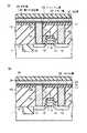
1 to 5 are sectional views showing a manufacturing process of a COP type FeRAM cell according to the first embodiment of the present invention.
[0020]
In this embodiment, a W plug is provided under the capacitor, and a laminated film (barrier layer) of a thin silicon carbide film and a thin titanium nitride film is provided between the W plug and the capacitor lower electrode (iridium film). A COP type FeRAM cell will be described.
[0021]
First, as shown in FIG. 1A, a
[0022]
Next, as shown in FIG. 1B, a
[0023]
First, a thin silicon oxide film (gate insulating film) 5 having a thickness of about 6 nm is formed on the exposed surface of the p-
[0024]
Next, n-type impurities are ion-implanted into the substrate surface using the gate upper insulating
[0025]
Next, a silicon nitride film to be a gate sidewall insulating film (spacer) 11 is formed on the entire surface so as to cover the side surface of the
[0026]
Next, a silicon oxide film is formed on the entire surface by a CVD process, and then the silicon oxide film is polished by a CMP process, thereby forming a
[0027]
Next, as shown in FIG. 2 (d), a
[0028]
First, a thin titanium film (not shown) is formed by sputtering or a CVD process so as to cover the side surface and the bottom surface of the
[0029]
Next, as shown in FIG. 2E, a
[0030]
Thereafter, as shown in FIG. 2E, a
[0031]
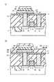
Next, as shown in FIG. 3F, a thin silicon carbide film (SiC film) 21 having a thickness of 10 nm or less is formed on the entire surface by a sputtering process, followed by a
[0032]
Instead of the
[0033]
Thereafter, the
[0034]
Here, since the thickness of the laminated film (barrier layer) of the
[0035]
Note that after forming the
[0036]
Further, FIG. 3G shows a state in which the
[0037]
In the RTA in the oxygen atmosphere, a part of oxygen in the atmosphere diffuses in the
[0038]
On the other hand, the
[0039]
Further, the laminated film of the
[0040]
Therefore, the laminated film of the
[0041]
Here, since SiC is a semiconductor, its resistance value varies greatly depending on the structure, formation method, presence / absence of doping, and the like. The resistivity value of β-SiC, which is a typical crystal structure, is 10-7× 10⁻⁶It is Ωcm, which is a high value compared to general metals, but has sufficient conductivity. Therefore, if the
[0042]
For example, when the thickness of the
[0043]
Hereinafter, the examination result about the laminated film of the SiC film | membrane and the film | membrane containing a metal carbide which became the motivation of this invention is demonstrated.
[0044]
Although the reactivity between SiC and the metal material (M) by heat treatment is generally low, the following reaction (1) or (2) may occur mainly depending on the metal material.
[0045]
(1) SiC + M → MSi + C
(2) SiC + M → MC + Si
Alternatively, both these reactions occur. Although what kind of reaction takes place is such that the Gibbs free energy associated with the reaction is minimized, there is no general guideline because it is a material-specific physical property.
[0046]
However, the inventors have determined that certain materials, specifically tungsten, platinum, ruthenium, iridium, SrRuOThreeFor metals such as these, it has been confirmed that the above reaction does not occur at normal capacitor process temperatures (temperatures required for crystallization of capacitor dielectric films). It has also been confirmed that the reaction between SiC and Si does not occur at normal capacitor process temperatures.
[0047]
On the other hand, for metal films made of metals such as titanium, zirconium, hafnium, vanadium, niobium, and tantalum, at least (2) of the above reaction occurs, and heat treatment is performed with these metal films and SiC films in contact with each other. In this case, it is confirmed that a metal carbide film is formed.
[0048]
Since the crystal structure of the metal carbide film takes a form in which carbon atoms enter between metal atoms, the effect of suppressing the diffusion of foreign elements from the outside is increased.
[0049]
Therefore, the diffusion barrier effect of the two-layer film of the SiC film and the metal carbide film generated by the reaction with the SiC film is further enhanced as compared with the case of the single-layer SiC film. That is, the effect of preventing permeation of oxygen during heat treatment in an oxygen atmosphere is further enhanced, and in addition, the effect of preventing mutual diffusion is also enhanced.
[0050]
In addition, since the metal carbide film itself retains metal conductivity, the use of a two-layer film of an SiC film and a metal carbide film for a contact portion such as a plug, compared with a case where a single-layer SiC film is used. Thus, the contact resistance can be reduced.
[0051]
In FIG. 6, a laminated film of a SiC film having a thickness of 7 nm and a titanium film having a thickness of 2.5 nm was formed on the W plug, and then a platinum film having a thickness of 50 nm was deposited on the laminated film. A cross-sectional SEM photograph after subjecting the sample (W / SiC / Ti / Pt structure) to oxygen annealing at 650 ° C. for 1 hour is shown. From FIG. 6, it is well known that oxygen diffuses easily in the platinum film, but nevertheless, the W plug is not oxidized at all. This is because the SiC film and the titanium film react to form a TiC / TiSi layer on the surface of the SiC layer, and a laminated film of the SiC film and the TiC / TiSi layer having a high oxygen diffusion suppression effect is formed.
[0052]
Returning to the process of the COP type FeRAM cell of this embodiment, after the step of FIG. 3 (g) described above, as shown in FIG. 4 (h), the second platinum film serving as the capacitor upper electrode on the
[0053]
The insulating
[0054]
Next, as shown in FIG. 4I, the
[0055]
Next, as shown in FIG. 5 (j), a resist mask (not shown) covering the
[0056]
Next, as shown in FIG. 5 (k), a
[0057]
Here, in the heat treatment under the oxidizing atmosphere, oxygen penetrates into the capacitor and contributes to the recovery of damage, while part of the oxygen reaches the capacitor lower electrode (
[0058]
SiC is a material that has a melting point of 2000 ° C. or higher and is extremely thermally stable and has extremely low oxygen permeability. Therefore, by disposing the
[0059]
Further, the laminated film of the
[0060]
On the other hand, the
[0061]
Thereafter, although not shown in the drawing, a well-known process, that is, a contact forming process that connects to the other of the source / drain diffusion layers 12 of the MOS transistor, a drive line forming process, a bit line forming process, and an upper metal wiring Through the wiring process, the FeRAM cell is completed.
[0062]
In the well-known process, for example, the contact forming process, it is necessary to cover a region to be etched including a step having a capacitor as a projection, excluding the etching region, with a resist (etching mask). At this time, as described above, according to the present embodiment, since the step with the capacitor as the convex portion is sufficiently small, the photolithography process can be easily performed with high accuracy, and as a result, the resist is easily and accurately formed. be able to.
[0063]
As described above, according to the present embodiment, by using the laminated film of the
[0064]
In this embodiment, the
[0065]
In this embodiment, PZT is used as the material for the capacitor dielectric film, and platinum or iridium is used as the material for the capacitor upper electrode / lower electrode. However, the material is not limited to such materials.
[0066]
For example, as a material of the capacitor dielectric film, SBT (SrBi2Ta2O9) And BIT (BiFourTiThreeO12It is also possible to use a ferroelectric material such as
[0067]
Here, since the crystallization temperature of SBT is about 750 ° C. and higher than the crystallization temperature of PZT (about 600 ° C.), heat treatment in a higher temperature oxidizing atmosphere is necessary when using SBT. It becomes. Therefore, the problem of oxidation of the plug directly under the capacitor (here, the W plug 20) becomes more serious. However, according to the present embodiment, the same effect can be expected even when a ferroelectric that requires heat treatment at a temperature higher than that of PZT is used.
[0068]
On the other hand, as the material of the capacitor upper electrode and lower electrode, ruthenium or strontium ruthenium oxide (SrRuOThreeIt is also possible to use compound conductors such as
[0069]
In this embodiment, a laminated film of the
[0070]
(Second Embodiment)
7 to 9 are cross-sectional views showing a manufacturing process of the COP type FeRAM cell according to the second embodiment of the present invention. The parts corresponding to those in FIGS. 1 to 5 are given the same reference numerals as in FIGS.
[0071]
The main difference between this embodiment and the first embodiment is that a polycrystalline silicon plug is provided under the capacitor, and SrRuO is provided on the lower and upper electrodes of the capacitor.ThreeThe film is used.
[0072]
First, as in the first embodiment, the steps of FIG. 1A to FIG. 1C are performed, and subsequently, as shown in FIG. A
[0073]
A specific method for forming the
[0074]
First, a polycrystalline silicon film is formed on the entire surface by a CVD process so as to fill the inside of the
[0075]
Next, as shown in FIG. 7B, a
[0076]
Next, as shown in FIG. 7B, a titanium film 34 having a thickness of about 2.5 nm, a
[0077]
Next, annealing is performed at 500 ° C. or higher in an inert gas or vacuum to react the
[0078]
At this time, the portion of the titanium film 34 in contact with the
[0079]
Next, as shown in FIG. 8D, a first SrRuO serving as a capacitor lower electrode is formed on the TiC / TiSi layer 26.ThreeA film 36 (film structure is amorphous) is formed by a sputtering process, followed by RTA at 600 ° C., and SrRuOThreeGood quality crystalline SrRuO that can be used as an electrode by crystallizing film 36Three
[0080]
Note that the TiC / TiSi layers 26 and 26 'may be formed by RTA in this step without the annealing in the step of FIG. 7C. However, as in the present embodiment, a thermal process for forming the TiC / TiSi layers 26 and 26 ', and SrRuOThreeBy separately providing the thermal process for crystallizing the
[0081]
Next, as shown in FIG. 8 (e), SrRuOThreeA
[0082]
In the RTA in the oxygen atmosphere, a part of the oxygen in the atmosphere diffuses in the
[0083]
Further, the laminated film of the TiC /
[0084]
Further, since SiC is a material that is extremely thermally stable and extremely low in oxygen permeability as described above, a plurality of SiC including RTA in the oxygen atmosphere performed after the formation of the
[0085]
On the other hand, the
[0086]
Thereafter, as shown in FIG. 8E, a second SrRuO as a capacitor upper electrode is formed on the PZT film 25.ThreeA
[0087]
Next, using the insulating
[0088]
Next, as shown in FIG. 9 (f), the second SrRuOThreeA resist mask (not shown) covering the
[0089]
Next, as shown in FIG. 9G, a
[0090]
Here, in the heat treatment under the oxidizing atmosphere, oxygen penetrates into the capacitor and contributes to damage recovery, while a part of the capacitor lower electrode (first SrRuOThreeAlthough the film 36) is also reached, since the oxygen diffusion suppressing effect of the laminated film of the TiC /
[0091]
Further, the laminated film of the TiC /
[0092]
Thereafter, although not shown in the drawing, a well-known process, that is, a contact forming process that connects to the other of the source / drain diffusion layers 12 of the MOS transistor, a drive line forming process, a bit line forming process, and an upper metal wiring The FeRAM is completed through the wiring process.
[0093]
As in the first embodiment, the resist (etching mask) required in the well-known process has a sufficiently small step with the capacitor as a protrusion, and can be easily and accurately formed.
[0094]
As described above, according to the present embodiment, by using a laminated film of the TiC /
[0095]
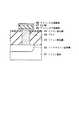
The inventors conducted experiments using a sample similar to the capacitor / plug structure of the present embodiment and confirmed the effect of the present embodiment. Specifically, first, on a polycrystalline silicon plug, a titanium silicide film (30 nm), a SiC film (7 nm), a titanium film (2.5 nm), an iridium film (50 nm), a platinum film (10 nm), SrRuOThreeA film (10 nm) and a PZT film (130 nm) are sequentially deposited, and a sample (Si / TiSi / SiC / Ti / Ir / Pt / SrRuO) is deposited.Three/ PZT structure) was prepared, and then the sample was subjected to oxygen annealing at 650 ° C. for 1 hour, and then the concentration profile in the depth direction of each element was measured by SIMS.
[0096]
The analysis result (voltage-residual polarization (V-Pr) characteristics) is shown in FIG. From FIG. 10, the polycrystalline silicon plug under the SiC film, the Ir film on the SiC film, and SrRuOThreeIt can be seen that no reaction and interdiffusion between the plug material (Si) and the electrode material (Ir, Ru, Pt) is observed with respect to the film and the Pt film (electrode).
[0097]
Further, in FIGS. 11A and 11B, the sample is subjected to the oxygen annealing, and SrRuO as a capacitor upper electrode is formed on the sample subjected to the oxygen annealing.ThreeThe hysteresis characteristics of a capacitor formed by sequentially forming a film, a platinum film, and a capacitor formed in the same manner by using the above sample without the Ti film are shown.
[0098]
From FIG. 11, it can be seen that by using a sample including a laminated film of an SiC film and a Ti film, better hysteresis characteristics can be obtained as compared with a sample of an SiC film alone without the Ti film.
[0099]
In the present embodiment, similarly to the first embodiment, for example, a zirconium film, a hafnium film, a vanadium film, a niobium film, or a tantalum film can be used instead of the
[0100]
In this embodiment, the material of the capacitor upper electrode and lower electrode is SrRuO.ThreeHowever, it is not limited to such a material. For example, BaRuOThreeIt is also possible to use conductive complex oxides such as noble metals, such as platinum, iridium or ruthenium, and oxides of these noble metals.
[0101]
(Third embodiment)
12 to 13 are cross-sectional views showing a manufacturing process of a COP type FeRAM cell according to the third embodiment of the present invention. The parts corresponding to those in FIGS. 1 to 5 are denoted by the same reference numerals as those in FIGS. 1 to 5, and detailed description thereof is omitted.
[0102]
The present embodiment is different from the first embodiment in that the W plug located under the capacitor is covered with a laminated film of a SiC film and a TiC / TiSi layer.
[0103]
First, as in the first embodiment, the steps of FIG. 1A to FIG. 1C are performed, and then the thickness of the inner wall of the
[0104]
Next, as shown in FIG. 12B, annealing is performed in an inert gas or vacuum to cause the
[0105]
Next, as shown in FIG. 13C, the
[0106]
Next, as shown in FIG. 13C, a
[0107]
Next, the steps of FIG. 3G to FIG. 5K described in the first embodiment are performed, and then the damage caused to the
[0108]
At this time, as in the first embodiment, some oxygen in the atmosphere reaches the capacitor lower electrode (the
[0109]
Similarly to the first embodiment, the
[0110]
On the other hand, the
[0111]
After this, although not shown in the drawing, a well-known process, that is, a contact forming process that connects to the other of the source / drain diffusion layers 10 of the MOS transistor, a drive line forming process, a bit line forming process, The FeRAM is completed through the wiring process.
[0112]
In this embodiment as well, as in the first embodiment, the thickness of the barrier layer can be reduced, the oxidation of the W plug 20 can be effectively prevented, and the FeRAM including the COP type FeRAM cell having high characteristics and reliability. Can be realized.
[0113]
Also in this embodiment, it is possible to use a capacitor dielectric film material other than PZT described in the first embodiment and a capacitor upper electrode / lower electrode material other than platinum.
[0114]
In addition, this invention is not limited to the said embodiment. For example, in the above-described embodiment, a memory cell having a structure in which a bit line is disposed on the upper layer of the capacitor has been described. The present invention can also be applied.
[0115]
Further, in the present invention, as shown in FIG. 14 (a), both ends of the capacitor (C) are connected between the source / drain of the cell transistor (T) to form a unit cell, and a plurality of unit cells are connected in series. The present invention can also be applied to a ferroelectric memory having a cell structure connected to (TC parallel unit serial connection type ferroelectric memory). FIG. 14B shows a cross-sectional view of the cell structure shown in FIG. In the figure, 51 is a semiconductor substrate, 52 is a source / drain diffusion layer, 53 is a gate insulating film, 54 is a gate electrode, 55 is an interlayer insulating film, 56 is a capacitor lower electrode, 57 is one of the capacitor lower electrode and the cell transistor T. , A capacitor dielectric film made of a ferroelectric material, 59 a capacitor upper electrode, 60 an interlayer insulating film, and 61 a capacitor upper electrode and the other source / drain of the cell transistor T Conductive plugs connecting the drain diffusion layer are shown.
[0116]
The present invention also provides Ta20Five,(Ba, Sr) Ti0ThreeThe present invention can also be applied to a stacked DRAM using a high dielectric material such as a capacitor dielectric film. Also in this case, the same effect as the above-described embodiment can be obtained with respect to the plug / capacitor structure.
[0117]
Furthermore, the above embodiments include inventions at various stages, and various inventions can be extracted by appropriately combining a plurality of disclosed constituent elements. For example, even if some constituent requirements are deleted from all the constituent requirements shown in the embodiment, if the problem described in the column of the problem to be solved by the invention can be solved, the configuration in which this constituent requirement is deleted Can be extracted as an invention.
[0118]
In addition, various modifications can be made without departing from the scope of the present invention.
[0119]
【The invention's effect】
As described above in detail, according to the present invention, after the conductive plug / electrode structure is formed, the oxidation of the conductive plug in the case where heat treatment in an oxidizing atmosphere is required is not hindered in miniaturization. A semiconductor device and a manufacturing method thereof that can be effectively prevented can be realized.
[Brief description of the drawings]
FIG. 1 is a cross-sectional view showing a manufacturing process of a COP type FeRAM cell according to a first embodiment of the present invention.
FIG. 2 is a cross-sectional view showing the manufacturing process of the COP type FeRAM cell following FIG.
3 is a cross-sectional view showing a manufacturing process of the COP type FeRAM cell following FIG. 2;
4 is a cross-sectional view showing the manufacturing process of the COP type FeRAM cell following FIG. 3;
FIG. 5 is a cross-sectional view showing a manufacturing process of the COP type FeRAM cell following FIG. 4;
FIG. 6 is a micrograph (cross-sectional SEM photograph) of a sample (W / SiC / Ti / Pt structure) subjected to oxygen annealing.
FIG. 7 is a cross-sectional view showing a manufacturing process of a COP type FeRAM cell according to a second embodiment of the present invention.
8 is a cross-sectional view showing the manufacturing process of the COP type FeRAM cell following FIG. 6;
9 is a cross-sectional view showing the manufacturing process of the COP type FeRAM cell following FIG. 7;
FIG. 10 shows a sample subjected to oxygen annealing (Si / TiSi / SiC / Ti / Ir / Pt / SrRuOThree/ PZT structure) shows the results of SIMS analysis
11 is a graph showing hysteresis characteristics of a capacitor formed using the sample of FIG. 10 and a capacitor formed using a structure in which the Ti film is omitted from the sample. FIG.
FIG. 12 is a cross-sectional view showing a manufacturing process of a COP type FeRAM cell according to a third embodiment of the present invention.
13 is a cross-sectional view showing the manufacturing process of the COP type FeRAM cell following FIG. 8;
FIG. 14 is an equivalent circuit diagram and a sectional view for explaining another embodiment of the present invention.
FIG. 15 is a sectional view showing a conventional COP structure.
[Explanation of symbols]
1 ... p-type silicon substrate
2 ... Groove
3. Insulating film
4 ... MOS transistor
5 ... Silicon oxide film
6 ... n-type polycrystalline silicon film
7. Tungsten silicide film
8 ... Silicon nitride film
9 ... Gate electrode
10 ... Extension
11 ... Gate sidewall insulating film
12 ... Source / drain diffusion layer
13 ... Silicon oxide film
14 ... Contact hole
15 ... Titanium nitride film
16 ... W plug
17 ... Silicon nitride film
18 ... Contact hole
19 ... Titanium nitride film
20 ... W plug
21 ... SiC film
22 ... Titanium film
23 ... Iridium film (capacitor lower electrode)
24. First platinum film (capacitor lower electrode)
25 ... PZT film (capacitor dielectric film)
26 ... TiC / TiSi layer
27 ... Second platinum film (capacitor upper electrode)
28. Insulating film mask
29 ... Silicon oxide film
30 ... polycrystalline silicon plug
31. Titanium silicide film
32 ... Silicon oxide film
33 ... Polycrystalline silicon plug
34 ... Titanium film
35. Titanium silicide film
36 ... The first SrRuOThreeMembrane (capacitor lower electrode)
37 ... Second SrRuOThreeMembrane (capacitor upper electrode)
38 ... SiC film
39 ... Titanium film
40 ... TiC / TiSi layer
Claims (4)
Translated fromJapanese前記導電性プラグ上に設けられた炭化珪素膜と、
前記炭化珪素膜上に設けられ、金属と炭素との金属炭化物、および、前記金属と珪素との金属珪化物を含む金属化合物膜であって、前記金属がチタン、ジルコニウム、ハフニウム、バナジウム、ニオブ、またはタンタルである前記金属化合物膜と、
前記金属化合物膜上に設けられたキャパシタ下部電極と、
前記キャパシタ下部電極上に設けられた強誘電体材料または高誘電体材料を主成分とするキャパシタ誘電体膜と、
前記キャパシタ誘電体膜上に設けられたキャパシタ上部電極と
を具備してなり、前記キャパシタ誘電体膜は酸化性雰囲気中での熱処理によりアモルファス構造の誘電体膜を結晶化する工程を経て形成されたものであり、前記金属炭化物、および、前記金属珪化物は、前記炭化珪素膜およびその上に形成した金属膜に対して前記熱処理を行うことで生じる、前記金属膜の構成金属と前記炭化珪素膜の構成炭素との反応で形成された金属炭化物、および、前記金属膜の構成金属と前記炭化珪素膜の構成珪素との反応で形成された金属珪化物であることを特徴とする半導体装置。A conductive plug provided on a semiconductor substrate;
A silicon carbide film provided on the conductive plug;
A metal compound film provided on the silicon carbide film and including a metal carbide of metal and carbon, and a metal silicide of the metal and silicon, wherein the metal is titanium, zirconium, hafnium, vanadium, niobium, Or the metal compound film that is tantalum;
A capacitor lower electrode provided on the metal compound film;
A capacitor dielectric film mainly composed of a ferroelectric material or a high dielectric material provided on the capacitor lower electrode;
A capacitor upper electrode provided on the capacitor dielectric film, wherein the capacitor dielectric film is formed through a step of crystallizing the amorphous dielectric film by heat treatment in an oxidizing atmosphere. The metal carbideand the metal silicide are produced by performing the heat treatment on the silicon carbide film and the metal film formed thereon, and the constituent metal of the metal film and the silicon carbide film And a metal silicide formed by a reaction between a constituent metal of the metal film and a constituent silicon of the silicon carbide film .
前記導電性プラグの上面を覆う炭化珪素膜を形成する工程と、
前記炭化珪素膜上に第1の金属膜を形成する工程であって、前記第1の金属膜がチタン膜、ジルコニウム膜、ハフニウム膜、バナジウム膜、ニオブ膜、またはタンタル膜である前記工程と、
前記第1の金属膜上に、キャパシタ下部電極としての第2の金属膜を形成する工程と、
前記第2の金属膜上に、キャパシタ誘電体膜としての、強誘電体材料または高誘電体材料を主成分とするアモルファス構造の誘電体膜を形成する工程と、
酸化性雰囲気中での熱処理により、前記炭化珪素膜上に、前記第1の金属膜の構成金属と炭素との金属炭化物、および、前記第1の金属膜の構成金属と珪素との金属珪素化物を含む金属化合物膜を形成するとともに、前記酸化性雰囲気中での熱処理により、前記アモルファス構造の誘電体膜を結晶化する工程であって、前記金属炭化物、および、前記金属珪化物は、前記炭化珪素膜およびその上に形成した前記第1の金属膜に対して前記熱処理を行うことで生じる、前記第1の金属膜の構成金属と前記炭化珪素膜の構成炭素との反応で形成された金属炭化物、および、前記第1の金属膜の構成金属と前記炭化珪素膜の構成珪素との反応で形成された金属珪化物である前記工程と
を有することを特徴とする半導体装置の製造方法。Forming a conductive plug on a semiconductor substrate;
Forming a silicon carbide film covering an upper surface of the conductive plug;
Forming a first metal film on the silicon carbide film, wherein the first metal film is a titanium film, a zirconium film, a hafnium film, a vanadium film, a niobium film, or a tantalum film;
Forming a second metal film as a capacitor lower electrode on the first metal film;
Forming a dielectric film having an amorphous structure mainly composed of a ferroelectric material or a high dielectric material as a capacitor dielectric film on the second metal film;
A metal carbide of the constituent metal of the first metal film and carbon and a metal silicide of the constituent metal of the first metal film and silicon are formed on the silicon carbide film by heat treatment in an oxidizing atmosphere. Forming a metal compound film containing the amorphous structure, and crystallizing the dielectric film having the amorphous structure by heat treatment in the oxidizing atmosphere, wherein the metal carbide and the metal silicide are formed by the carbonization. Metal formed by reaction of constituent metal of the first metal film and constituent carbon of the silicon carbide film generated by performing the heat treatment on the silicon film and the first metal film formed thereon A method of manufacturing a semiconductor device, comprising: a carbide, and the step of forming a metal silicide formed by a reaction between a constituent metal of the first metal film and a constituent silicon of the silicon carbide film .
Priority Applications (2)
| Application Number | Priority Date | Filing Date | Title |
|---|---|---|---|
| JP2002293902AJP4445191B2 (en) | 2002-10-07 | 2002-10-07 | Semiconductor device and manufacturing method thereof |
| US10/678,061US7151288B2 (en) | 2002-10-07 | 2003-10-06 | Semiconductor device and method of manufacturing the same |
Applications Claiming Priority (1)
| Application Number | Priority Date | Filing Date | Title |
|---|---|---|---|
| JP2002293902AJP4445191B2 (en) | 2002-10-07 | 2002-10-07 | Semiconductor device and manufacturing method thereof |
Publications (2)
| Publication Number | Publication Date |
|---|---|
| JP2004128406A JP2004128406A (en) | 2004-04-22 |
| JP4445191B2true JP4445191B2 (en) | 2010-04-07 |
Family
ID=32284675
Family Applications (1)
| Application Number | Title | Priority Date | Filing Date |
|---|---|---|---|
| JP2002293902AExpired - Fee RelatedJP4445191B2 (en) | 2002-10-07 | 2002-10-07 | Semiconductor device and manufacturing method thereof |
Country Status (2)
| Country | Link |
|---|---|
| US (1) | US7151288B2 (en) |
| JP (1) | JP4445191B2 (en) |
Families Citing this family (9)
| Publication number | Priority date | Publication date | Assignee | Title |
|---|---|---|---|---|
| US7015564B2 (en)* | 2003-09-02 | 2006-03-21 | Matsushita Electric Industrial Co., Ltd. | Capacitive element and semiconductor memory device |
| KR100563487B1 (en)* | 2003-12-31 | 2006-03-27 | 동부아남반도체 주식회사 | Metal wiring formation method of semiconductor device |
| JP2006269800A (en)* | 2005-03-24 | 2006-10-05 | Toshiba Corp | Semiconductor device |
| JP4445445B2 (en)* | 2005-09-07 | 2010-04-07 | 株式会社東芝 | Semiconductor device and manufacturing method thereof |
| US8730647B2 (en)* | 2008-02-07 | 2014-05-20 | Ibiden Co., Ltd. | Printed wiring board with capacitor |
| JP5487625B2 (en)* | 2009-01-22 | 2014-05-07 | ソニー株式会社 | Semiconductor device |
| JP5707907B2 (en)* | 2010-12-06 | 2015-04-30 | 株式会社リコー | Piezoelectric actuator, droplet discharge head, and droplet discharge device |
| JP5811728B2 (en)* | 2011-09-16 | 2015-11-11 | 株式会社リコー | ELECTRO-MACHINE CONVERSION ELEMENT, DROPLET DISCHARGE HEAD, DROPLET DISCHARGE DEVICE, AND IMAGE FORMING DEVICE |
| US10406774B2 (en)* | 2016-10-17 | 2019-09-10 | U.S. Department Of Energy | Diffusion bonding of silicon carbide using iridium and hermetic silicon carbide-iridium bonds |
Family Cites Families (11)
| Publication number | Priority date | Publication date | Assignee | Title |
|---|---|---|---|---|
| JPH0730111A (en)* | 1993-07-15 | 1995-01-31 | Hitachi Ltd | Insulated gate type field effect transistor |
| US5554564A (en)* | 1994-08-01 | 1996-09-10 | Texas Instruments Incorporated | Pre-oxidizing high-dielectric-constant material electrodes |
| JPH09252095A (en) | 1996-03-18 | 1997-09-22 | Toshiba Corp | Thin film capacitor and semiconductor device |
| US6346741B1 (en)* | 1997-11-20 | 2002-02-12 | Advanced Technology Materials, Inc. | Compositions and structures for chemical mechanical polishing of FeRAM capacitors and method of fabricating FeRAM capacitors using same |
| JP2001267516A (en) | 2000-03-16 | 2001-09-28 | Toshiba Corp | Ferroelectric memory |
| US6680514B1 (en)* | 2000-12-20 | 2004-01-20 | International Business Machines Corporation | Contact capping local interconnect |
| US6656830B1 (en)* | 2001-02-07 | 2003-12-02 | Advanced Micro Devices, Inc. | Dual damascene with silicon carbide middle etch stop layer/ARC |
| JP2002289810A (en) | 2001-03-28 | 2002-10-04 | Toshiba Corp | Semiconductor device and method of manufacturing the same |
| US20030062596A1 (en)* | 2001-10-02 | 2003-04-03 | Actel Corporation | Metal-to-metal antifuse employing carbon-containing antifuse material |
| KR100422597B1 (en)* | 2001-11-27 | 2004-03-16 | 주식회사 하이닉스반도체 | Method of forming semiconductor device with capacitor and metal-interconnection in damascene process |
| US6693356B2 (en)* | 2002-03-27 | 2004-02-17 | Texas Instruments Incorporated | Copper transition layer for improving copper interconnection reliability |
- 2002
- 2002-10-07JPJP2002293902Apatent/JP4445191B2/ennot_activeExpired - Fee Related
- 2003
- 2003-10-06USUS10/678,061patent/US7151288B2/ennot_activeExpired - Fee Related
Also Published As
| Publication number | Publication date |
|---|---|
| US20040130026A1 (en) | 2004-07-08 |
| JP2004128406A (en) | 2004-04-22 |
| US7151288B2 (en) | 2006-12-19 |
Similar Documents
| Publication | Publication Date | Title |
|---|---|---|
| JP5047250B2 (en) | Manufacturing method of semiconductor device | |
| KR100423906B1 (en) | Ferroelectric memory device amd method of forming the same | |
| JP3495955B2 (en) | Semiconductor memory device and method of manufacturing the same | |
| JPH09102591A (en) | Semiconductor device and manufacturing method thereof | |
| JP2010016036A (en) | Semiconductor device, and method for manufacturing the same | |
| JP4445191B2 (en) | Semiconductor device and manufacturing method thereof | |
| JP2005057103A (en) | Semiconductor device and manufacturing method thereof | |
| JP4105656B2 (en) | Semiconductor device and manufacturing method thereof | |
| JP5018772B2 (en) | Manufacturing method of semiconductor device | |
| JP2004356464A (en) | Method of manufacturing ferroelectric element, ferroelectric element, and FeRAM | |
| JP2002203948A (en) | Semiconductor device | |
| US7573120B2 (en) | Semiconductor device and method of manufacturing the same | |
| WO2000046856A1 (en) | Capacitor and method of its manufacture | |
| JP2003051582A (en) | Semiconductor device and method of manufacturing the same | |
| JP2002373975A (en) | Method of manufacturing ferroelectric memory device and ferroelectric memory device | |
| JP5487140B2 (en) | Manufacturing method of semiconductor device | |
| JP2005129852A (en) | Semiconductor device | |
| JP4749218B2 (en) | Method for manufacturing ferroelectric element | |
| JP2002094014A (en) | Semiconductor memory device and method of manufacturing the same | |
| JP5007723B2 (en) | Semiconductor device including capacitor and manufacturing method thereof | |
| KR100652354B1 (en) | Capacitor of semiconductor device having low contact resistance between lower electrode and contact plug, and method of manufacturing same | |
| JP5326256B2 (en) | Manufacturing method of semiconductor device | |
| JP2006269800A (en) | Semiconductor device | |
| JP2004241679A (en) | Semiconductor device and manufacturing method thereof | |
| JP2007266023A (en) | Semiconductor device and manufacturing method of semiconductor device |
Legal Events
| Date | Code | Title | Description |
|---|---|---|---|
| A621 | Written request for application examination | Free format text:JAPANESE INTERMEDIATE CODE: A621 Effective date:20050926 | |
| A977 | Report on retrieval | Free format text:JAPANESE INTERMEDIATE CODE: A971007 Effective date:20080529 | |
| A131 | Notification of reasons for refusal | Free format text:JAPANESE INTERMEDIATE CODE: A131 Effective date:20080617 | |
| A521 | Request for written amendment filed | Free format text:JAPANESE INTERMEDIATE CODE: A523 Effective date:20080815 | |
| A131 | Notification of reasons for refusal | Free format text:JAPANESE INTERMEDIATE CODE: A131 Effective date:20090929 | |
| A521 | Request for written amendment filed | Free format text:JAPANESE INTERMEDIATE CODE: A523 Effective date:20091127 | |
| TRDD | Decision of grant or rejection written | ||
| A01 | Written decision to grant a patent or to grant a registration (utility model) | Free format text:JAPANESE INTERMEDIATE CODE: A01 Effective date:20091222 | |
| A01 | Written decision to grant a patent or to grant a registration (utility model) | Free format text:JAPANESE INTERMEDIATE CODE: A01 | |
| A61 | First payment of annual fees (during grant procedure) | Free format text:JAPANESE INTERMEDIATE CODE: A61 Effective date:20100115 | |
| FPAY | Renewal fee payment (event date is renewal date of database) | Free format text:PAYMENT UNTIL: 20130122 Year of fee payment:3 | |
| LAPS | Cancellation because of no payment of annual fees |