JP4443067B2 - Processor and reset control method thereof - Google Patents
Processor and reset control method thereofDownload PDFInfo
- Publication number
- JP4443067B2 JP4443067B2JP2001129781AJP2001129781AJP4443067B2JP 4443067 B2JP4443067 B2JP 4443067B2JP 2001129781 AJP2001129781 AJP 2001129781AJP 2001129781 AJP2001129781 AJP 2001129781AJP 4443067 B2JP4443067 B2JP 4443067B2
- Authority
- JP
- Japan
- Prior art keywords
- signal
- reset signal
- processor
- input
- register
- Prior art date
- Legal status (The legal status is an assumption and is not a legal conclusion. Google has not performed a legal analysis and makes no representation as to the accuracy of the status listed.)
- Expired - Fee Related
Links
Images


Classifications
- G—PHYSICS
- G06—COMPUTING OR CALCULATING; COUNTING
- G06F—ELECTRIC DIGITAL DATA PROCESSING
- G06F1/00—Details not covered by groups G06F3/00 - G06F13/00 and G06F21/00
- G06F1/24—Resetting means
Landscapes
- Engineering & Computer Science (AREA)
- Theoretical Computer Science (AREA)
- Physics & Mathematics (AREA)
- General Engineering & Computer Science (AREA)
- General Physics & Mathematics (AREA)
- Microcomputers (AREA)
- Multi Processors (AREA)
- Retry When Errors Occur (AREA)
Description
Translated fromJapanese【0001】
【発明の属する技術分野】
本発明は、プロセッサおよびそのリセット制御方法に関し、特に携帯端末、携帯電話またはデジタルカメラなどに使用されるプロセッサに適用して好適な技術に関する。
【0002】
【従来の技術】
一般に、プロセッサの中には、リセット信号によりリセット割り込みを発生し、システムの初期化プログラムを実行することにより、プロセッサおよびそのプロセッサにより構成されるシステムの状態を適切に設定する機構を備えたものがある。
【0003】
上述した機構を備えたプロセッサでは、電源投入やリセットボタンの押下などに起因して外部からリセット信号が入力されると、まずプロセッサ内部の記憶素子を初期化する起動リセット動作が実行される。つづいて、プロセッサの内部でリセット割り込みが発生し、リセットベクタと呼ばれる初期化処理用のプログラムが、プロセッサの外部にバスを介して接続されたROM(リード・オンリー・メモリ)から読み込まれる。この初期化処理用のプログラムの実行によって、プロセッサ内部あるいはシステム上に存在する各デバイスの各設定用レジスタが設定される。このようにして、種々のアプリケーションプログラムを実行可能な状態に環境が整えられる。
【0004】
ところで、プロセッサの低消費電力化を図るため、一定時間の間、何らかの必要とされる処理がプロセッサに発行されない場合に、プロセッサに供給するクロックを停止させる機能がある。このような機能を有するプロセッサでは、クロック停止後にプロセッサの動作を回復させるため、リセット信号を再度入力するようになっているのが一般的である。
【0005】
【発明が解決しようとする課題】
しかしながら、ROMは低速なメモリデバイスであるため、クロックの停止等によるプロセッサの停止状態からプロセッサを再起動させてすべての初期設定処理を終えるまでに時間がかかるという問題点がある。特に、頻繁にプロセッサの停止とリセット信号による再起動がおこなわれるシステムでは、再起動時にROMへのアクセスが毎回実行されることによるシステムの起動待ち時間が増大するという問題点がある。
【0006】
本発明は、上記問題点に鑑みてなされたものであって、停止状態からの再起動が高速におこなえるプロセッサを提供することを目的とする。また、本発明の他の目的は、停止状態からプロセッサを高速に再起動させることができるリセット制御方法を提供することである。
【0007】
【課題を解決するための手段】
リセット信号によって初期設定される領域を、たとえばプロセッサとプロセッサの外部とのコミュニケーションをおこなうために必須となるレジスタ群よりなる第1の初期設定領域と、第1の初期設定領域のレジスタ群およびプロセッサの内部の命令の実行に関するレジスタ群の両方を除く第2の初期設定領域と、プロセッサの内部の命令の実行に関するレジスタ群よりなる第3の初期設定領域とに分ける。第1の初期設定領域は、第1のリセット信号に基づいて初期設定される領域とする。第2の初期設定領域は、第1のリセット信号と第2のリセット信号のどちらかに基づいて初期設定される領域とする。第3の初期設定領域は、第1のリセット信号、第2のリセット信号、第3のリセット信号のどれか一つに基づいて初期設定される領域とする。
【0008】
そして、第1、第2および第3の各初期設定領域にそれぞれ対応する第1、第2および第3のフラグをさらに設ける。第1のリセット信号によってすべてのフラグがクリアとなる。第2のリセット信号によって第1のフラグを除く残りのフラグがクリアされる。第3のリセット信号によって第3のフラグのみがクリアとなる。第1のフラグは、第1の初期設定領域の初期設定処理が完了すると、セットされる。第2のフラグおよび第3のフラグは、それぞれ第2の初期設定領域および第3の初期設定領域の初期設定処理が完了すると、セットされる。
【0009】
この発明によれば、第1のリセット信号によってプロセッサ全体が初期設定されるが、第2のリセット信号によっては、プロセッサとプロセッサの外部とのコミュニケーションをおこなうために必須となるレジスタ群を除く領域が初期設定される。また、第3のリセット信号によっては、プロセッサの内部の命令の実行に関するレジスタ群のみが初期設定される。
【0010】
【発明の実施の形態】
以下に、本発明の実施の形態について図面を参照しつつ詳細に説明する。図1は、本発明の実施の形態にかかるプロセッサの要部の構成を示すブロック図である。このプロセッサ1は、命令フェッチ制御部11、命令実行部12、キャッシュメモリおよびキャッシュ制御部よりなるキャッシュユニット13、バス制御部14、クロック制御部15、第1のレジスタ群16、リセットレジスタ(RSTR)2および設定完了表示レジスタ(RSTCR)3を備えている。
【0011】
命令フェッチ制御部11、命令実行部12およびキャッシュユニット13には、それぞれ1または2以上のレジスタよりなる第2、第3および第4のレジスタ群41,42,43が設けられている。キャッシュユニット13内の第4のレジスタ群43には、たとえば論理アドレスを物理アドレスに変換するためのレジスタ対(LPFRおよびPPFR)44が設けられている。
【0012】
また、バス制御部14には、プロセッサ1に対してローカルメモリとなるRAM5のアドレス範囲の開始アドレスおよび比較禁止ビットを設定するレジスタ対(ASRおよびAMR)45が設けられている。プロセッサ1は、バス制御部14により制御されるデータバスおよびアドレスバスを介して図示しないROMに接続される。なお、図1においては、本発明に関係のない構成については図示省略されている。
【0013】
この実施の形態では、第1のレジスタ群16と、ASRおよびAMRで表される、RAM5(ローカルメモリ)に対するアドレス設定レジスタ45は、第1のリセット信号であるPRST信号が発生した場合に初期設定処理の対象となる。バス制御部14に設けられた他のレジスタは、PRST信号または第2のリセット信号であるHRST信号が発生した場合に初期設定処理の対象となる。第2、第3および第4のレジスタ群41,42,43は、PRST信号、HRST信号または第3のリセット信号であるSRST信号が発生した場合に初期設定処理の対象となる。
【0014】
つまり、PRST信号が発生すると、第1のレジスタ群16、ASRおよびAMRで表されるアドレス設定レジスタ45、バス制御部14に設けられたレジスタのうち、ASRおよびAMRで表されるアドレス設定レジスタ45を除くレジスタ、第2、第3および第4のレジスタ群41,42,43が初期設定処理の対象となる。HRST信号が発生すると、バス制御部14に設けられたレジスタのうち、ASRおよびAMRで表されるアドレス設定レジスタ45を除くレジスタ、第2、第3および第4のレジスタ群41,42,43が初期設定処理の対象となる。
【0015】
また、HRST信号の発生により、クロック制御部15内の、プロセッサ内部へのクロックの供給を停止させているレジスタ(図示せず)がリセットされる。それによって、クロック制御部15は、外部から供給されたクロックの、プロセッサ各部への供給を再開する。SRST信号が発生すると、第2、第3および第4のレジスタ群41,42,43が初期設定処理の対象となる。
【0016】
したがって、この実施の形態では、第1のレジスタ群16と、ASRおよびAMRで表されるアドレス設定レジスタ45は、第1の初期設定領域に相当する。また、バス制御部14に設けられたレジスタのうち、ASRおよびAMRで表されるアドレス設定レジスタ45を除くレジスタは、第2の初期設定領域に相当する。
【0017】
また、第2、第3および第4のレジスタ群41,42,43は第3の初期設定領域に相当する。図1において、符号17は、外部からPRST信号が入力される端子(PRST端子)であり、符号18は、外部からHRST信号が入力される端子(HRST端子)であり、符号19は、外部からSRST信号が入力される端子(SRST端子)である。また、符号10は、外部からクロックが入力される端子(CLOCK端子)である。
【0018】
図2は、第1の初期設定領域に含まれるレジスタの一例を示す図表である。この一覧表において、ARS0〜ARS3はDRAMのアドレス領域設定レジスタである。AMK0〜AMK3はDRAMのアドレスマスクレジスタである。DCTLは、DRAM品種ごとに異なるDRAMのオペレーション間の最小サイクル数の設定をおこなうDRAMコントロールレジスタである。DAMCは、DRAMに対するアクセスのモードを選択するためのDRAMアクセスモード制御レジスタである。
【0019】
DCFGは、DRAMタイプ、DRAMバスのバス幅、DRAM直結/DIMM使用などの表示および設定をおこなうDRAMコンフィギュレーションレジスタである。DANは、4本のDCSに接続するDRAMのRASアドレスビット数、CASアドレスビット数、およびバンクアドレスビット数を設定するためのDRAMアドレスナンバレジスタである。
【0020】
DSTSは、SDRAMコントローラの状態を表すDRAMステータスレジスタである。DRCNは、SDRAMのリフレッシュとして、オートリフレッシュおよびセルフリフレッシュをサポートするDRAMリフレッシュコントロールレジスタである。DARTは、オートリフレッシュ時のリフレッシュ間隔を規定するためのDRAMオートリフレッシュタイマレジスタである。その他、図2の表には記載されていないが、第1のレジスタ群16には、DRAMのメモリ領域のアドレス範囲を設定するためのDRAMアドレス領域設定レジスタ(DARS)、およびDRAMのアドレス範囲を設定するためのDRAMアドレスマスクレジスタ(DAMK)などが含まれる。ここでは、DRAMはプロセッサ1のローカルなメモリであるRAM5である。
【0021】
図3は、リセットレジスタ2の構成を示す概略図である。リセットレジスタ2はHSビット21とSSビット22を有する。HSビット21に書き込みをおこなうことによって、HRST端子18から入力されるリセット信号であるHRST信号と同等の信号がプロセッサ1の内部でアサートされる。また、SSビット22に書き込みをおこなうことによって、SRST端子19から入力されるリセット信号であるSRST信号と同等の信号がプロセッサ1の内部でアサートされる。
【0022】
図4は、プロセッサ1の初期化制御部の構成を示す回路図である。なお、この初期化制御部は図1では省略されている。PRST端子17を介して外部から入力されたPRST信号はそのままプロセッサ1内に供給される。
【0023】
HRST端子18を介して外部から入力されたHRST信号(以下、外部HRST信号とする)は、オア回路61の一方の入力端子に入力される。また、リセットレジスタ2のHSビット21への書き込み信号はフリップフロップ62に入力され、このフリップフロップ62の出力信号がオア回路61のもう一方の入力端子に入力される。すなわち、外部HRST信号の入力またはHSビット21への書き込みによって、HRST信号またはそれと同等の信号(以下、内部HRST信号とする)がアサートされる。HSビット21への書き込み信号は複数のフリップフロップ63,64,65,・・・からなるシフトレジスタに供給される。
【0024】
このシフトレジスタを構成する複数のフリップフロップ63,64,65,・・・の各出力信号はノア回路66に入力される。ノア回路66の出力信号は、HSビット21への書き込み信号が入力されるフリップフロップ62のイネーブル端子(EN)に入力される。これによって、HSビット21への書き込み信号がシフトレジスタにおいてシフトされている間は、内部HRST信号が発生し続けることになる。
【0025】
SRST端子19を介して外部から入力されたSRST信号(以下、外部SRST信号とする)、およびリセットレジスタ2のSSビット22への書き込みによって発生する、外部SRST信号と同等の信号(以下、内部SRST信号とする)についても同様である。すなわち、SSビット22への書き込み信号は複数のフリップフロップ73,74,75,・・・からなるシフトレジスタに供給される。このシフトレジスタの各段の出力信号は、ノア回路76を介して、SSビット22への書き込み信号が入力されるフリップフロップ72のイネーブル端子(EN)に供給される。それによって、シフトレジスタにおいてSSビット22への書き込み信号のシフトが終了するまで、内部SRST信号が発生し続ける。この内部SRST信号および外部SRST信号はオア回路71に入力され、アサートされる。
【0026】
図5は、設定完了表示レジスタ3の構成を示す概略図である。設定完了表示レジスタ3はPCビット31とHCビット32とSCビット33を有する。PCビット31は第1のフラグを格納する。第1のフラグは、第1の初期設定領域の初期設定処理が済んでいるか否かを表す。HCビット32は第2のフラグを格納する。第2のフラグは、第2の初期設定領域の初期設定処理が済んでいるか否かを表す。SCビット33は第3のフラグを格納する。第3のフラグは、第3の初期設定領域の初期設定処理が済んでいるか否かを表す。
【0027】
図6は、設定完了表示レジスタ3の要部の構成を示す回路図である。設定完了表示レジスタ3は、PCビット31、HCビット32およびSCビット33にそれぞれ対応するフリップフロップ81,82,83を有する。PCビット31のフリップフロップ81のリセット端子にはPRST信号が入力される。フリップフロップ81の入力端子には、第1の初期設定領域の初期設定処理の完了によって発生する信号、すなわちPCビット31の第1のフラグをセットするための信号(以下、PCセット信号とする)がオア回路84を介して入力される。このオア回路84には、フリップフロップ81の出力信号も入力される。つまり、PCビット31は、PRST信号がアサートされるとリセットされ、PCセット信号が入力されると、つぎにPRST信号がアサートされるまでフラグをセットした状態を保持する。
【0028】
HCビット32のフリップフロップ82のリセット端子には、PRST信号、および内部もしくは外部のHRST信号を入力とするオア回路85の出力信号が入力される。フリップフロップ82の入力端子には、第2の初期設定領域の初期設定処理の完了によって発生する信号、すなわちHCビット32の第2のフラグをセットするための信号(以下、HCセット信号とする)がオア回路86を介して入力される。このオア回路86には、フリップフロップ82の出力信号も入力される。したがって、HCビット32は、PRST信号、または内部もしくは外部のHRST信号がアサートされるとリセットされ、HCセット信号が入力されると、つぎにPRST信号、または内部もしくは外部のHRST信号がアサートされるまでフラグをセットした状態を保持する。
【0029】
SCビット33のフリップフロップ83のリセット端子には、PRST信号、内部もしくは外部のHRST信号、および内部もしくは外部のSRST信号を入力とするオア回路87の出力信号が入力される。フリップフロップ83の入力端子には、第3の初期設定領域の初期設定処理の完了によって発生する信号、すなわちSCビット33の第3のフラグをセットするための信号(以下、SCセット信号とする)がオア回路88を介して入力される。このオア回路88には、フリップフロップ83の出力信号も入力される。したがって、SCビット33は、PRST信号、内部もしくは外部のHRST信号、または内部もしくは外部のSRST信号がアサートされるとリセットされる。
【0030】
そして、SCビット33は、SCセット信号が入力されると、つぎにPRST信号、内部もしくは外部のHRST信号、または内部もしくは外部のSRST信号がアサートされるまでフラグをセットした状態を保持する。なお、プロセッサ1のハードウェアが自動的に初期化シーケンスを発生させる機構を有している場合には、PCビット31、HCビット32およびSCビット33は、その設定シーケンスの完了をもって自動的にセットされる。そして、PCビット31、HCビット32およびSCビット33は、対応するシーケンサ部分の初期化をおこなうリセット信号によりリセットされる。
【0031】
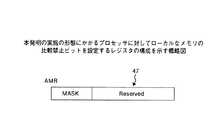
図7および図8は、プロセッサ1に対してローカルなメモリであるRAM5のアドレス範囲の開始アドレスおよび比較禁止ビットを設定するレジスタ対(ASRおよびAMR)45の、それぞれ開始アドレスを設定するレジスタ(ASR)46および比較禁止ビットを設定するレジスタ(AMR)47の構成を示す概略図である。また、図9は、開始アドレスを設定するレジスタ(ASR)46および比較禁止ビットを設定するレジスタ(AMR)47に基づいてRAM5にアサインされる番地の概略を示すメモリマップ図である。開始アドレスを設定するレジスタ(ASR)46により設定されるアドレスのうち、比較禁止ビットを設定するレジスタ(AMR)47によりマスクされない上位ビットで表されるアドレスがRAM5の領域のアドレスとなる。
【0032】
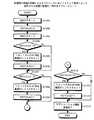
つぎに、上述したプロセッサ1の起動シーケンスの実施例について説明する。まず、電源投入時にPRST信号がアサートされた場合の初期化シーケンスについて図10に示すフローチャートを参照しながら説明する。図10のフローチャートにおいて、まず、PRST信号がアサートされると(ステップS1001)、設定完了表示レジスタ(RSTCR)3のPCビット31、HCビット32およびSCビット33がたとえば「0」にリセットされる(ステップS1002)。その後、PRST信号がネゲートされると(ステップS1003)、たとえば「0xFF00_0000」の初期アドレスからの命令フェッチ要求が発行される。ここで、電源投入直後はRAM5に有効なデータが保持されていないため、プロセッサ1は外部バス上のROMにアクセスする。
【0033】
このROMに格納されている初期化プログラムはPCビット31の値を参照し(ステップS1004)、その値がたとえば「0」であることを認識する(ステップS1004:Yes)。それによって、PRST信号がアサートされた場合に必要な処理を含むルーチンが実行される。プロセッサ1が起動した後、RAM5をアクセスするためのアドレス情報が、たとえばアドレス範囲の開始アドレスを設定するレジスタ(ASR)46およびアドレス範囲の比較禁止ビットを設定するレジスタ(AMR)47に設定される。
【0034】
たとえば、開始アドレスを設定するレジスタ(ASR)46に「0x0000_0000」が設定され、比較禁止ビットを設定するレジスタ(AMR)47に「0x01FF_FFFF」が設定されることによって、「0x0000_0000」番地から「0x01FF_FFFF」番地までがRAM5にアサインされる。また、第1のレジスタ群16も設定され、第1の初期設定領域に含まれるレジスタのセットが完了する(ステップS1005)。この時点で初期化プログラムはPCビット31に書き込みをおこない、このビットをたとえば「1」にセットする(ステップS1006)。
【0035】
しかる後、初期化プログラムはHCビット32の値を参照する(ステップS1007)。ここでは、ステップS1002でHCビット32をリセットしているため、当然のことながらHCビット32の値は「0」である(ステップS1007:Yes)。したがって、外部または内部のHRST信号がアサートされた場合に必要な処理を含むルーチンが実行され、第2の初期設定領域に含まれるレジスタのセットが完了する(ステップS1008)。そして、初期化プログラムはHCビット32に書き込みをおこない、このビットをたとえば「1」にセットする(ステップS1009)。
【0036】
つづいて、初期化プログラムはSCビット33の値を参照する(ステップS1010)。HCビット32と同様に、ここでも当然のことながらSCビット33の値は「0」である(ステップS1010:Yes)。したがって、外部または内部のSRST信号がアサートされた場合に必要な処理を含むルーチンが実行され、第3の初期設定領域に含まれるレジスタのセットが完了する(ステップS1011)。そして、初期化プログラムはSCビット33に書き込みをおこない、このビットをたとえば「1」にセットする(ステップS1012)。以上の処理によって、アプリケーションを開始する準備が完了する(ステップS1013)。
【0037】
つぎに、プロセッサ1の起動後、一定時間必要とされる処理がプロセッサ1に発行されなかったことを契機としてプロセッサ1が自らクロック制御部15に対してすべてのクロックを停止させた状態において、必要性が発生した時点で外部HRST信号により再起動がおこなわれる場合の再起動シーケンスについて図11に示すフローチャートを参照しながら説明する。図11のフローチャートにおいて、まず外部よりHRST信号がアサートされる(ステップS1101)。
【0038】
それによって、クロック制御部15でクロックを停止させているレジスタがリセットされ、プロセッサ1の内部へのクロックの供給が開始される。また、設定完了表示レジスタ(RSTCR)3のHCビット32およびSCビット33がたとえば「0」にリセットされる(ステップS1102)。その際、PCビット31に対するリセット動作はおこなわれない。したがって、RAM5には有効なデータが保持されたままである。
【0039】
つぎに、外部HRST信号がネゲートされると(ステップS1103)、RAM5に格納されている初期化プログラムはPCビット31の値を参照する(ステップS1104)。PCビット31の値が「1」であれば(ステップS1104:No)、第1の初期設定領域に含まれるレジスタはすべてセットされた状態であるため、第1の初期設定領域に対する初期設定処理(ステップS1105、ステップS1106)は省略される。
【0040】
そして、初期化プログラムはHCビット32の値を参照する(ステップS1107)。ここでは、HCビット32の値は当然のことながら「0」であるため(ステップS1107:Yes)、第2の初期設定領域に含まれるレジスタがセットされ(ステップS1108)、HCビット32の値が「1」にセットされる(ステップS1109)。
【0041】
つづいて、初期化プログラムはSCビット33の値を参照する(ステップS1110)が、SCビット33の値も当然のことながら「0」であるため(ステップS1110:Yes)、第3の初期設定領域に含まれるレジスタがセットされ(ステップS1111)、その後にSCビット33の値が「1」にセットされる(ステップS1112)。以上の処理によって、アプリケーションを開始する準備が完了する(ステップS1113)。なお、図11に示す再起動シーケンスは、内部HRST信号がアサートされた場合も同様である。
【0042】
ここで、ステップS1102において設定完了表示レジスタ(RSTCR)3のPCビット31をリセットしていないにもかかわらず、ステップS1104においてPCビット31の値を参照する理由は、たとえばPRST信号のアサートによって図10に示す初期化シーケンスの実行中で、第1の初期設定領域の初期設定処理が完了していないときに、外部HRST信号または内部HRST信号がアサートされた場合に、第1の初期設定領域の初期設定処理を完了させる必要があるからである。これは、本実施の形態のプロセッサ1が設定完了表示レジスタ(RSTCR)3を備えており、このレジスタを参照すれば各初期設定領域の初期設定処理が完了しているか否かを知ることができる構成となっていることにより実現される。
【0043】
したがって、設定完了表示レジスタ(RSTCR)3を設けずに、複数のリセット信号と各リセット信号に対応する複数の初期設定領域を設け、アサートされたリセット信号に対応する領域の初期設定処理をおこなう構成とした場合には、PRST信号のアサートによる初期化シーケンスの実行中に外部HRST信号または内部HRST信号がアサートされると、第1の初期設定領域の初期設定が完全におこなわれないまま、第2および第3の初期設定領域の初期設定処理が完了してしまう場合がある。つまりプロセッサ1が完全な起動状態にならないという不具合が発生してしまう。
【0044】
このような不具合の発生を防ぐために、ステップS1104でPCビット31の値を参照する。そして、その値がリセットされた値であれば、第1の初期設定領域の初期設定処理をおこなう(ステップS1105)。その後、PCビット31の値をセットし(ステップS1106)、ステップS1107へ進む。
【0045】
つぎに、外部SRST信号または内部SRST信号による起動処理シーケンスについて図12に示すフローチャートを参照しながら説明する。図12のフローチャートにおいて、まず外部または内部のSRST信号がアサートされると(ステップS1201)、命令フェッチ制御部11、命令実行部12およびキャッシュユニット13内のすべてのレジスタが初期化される。また、設定完了表示レジスタ(RSTCR)3のSCビット33がたとえば「0」にリセットされる(ステップS1202)。その際、PCビット31とHCビット32に対するリセット動作はおこなわれない。
【0046】
内部または外部のSRST信号がネゲートされると(ステップS1203)、「0xFF00_0000」の初期アドレスからの命令フェッチ要求が発行される。RAM5に格納されている初期化プログラムはPCビット31の値を参照し(ステップS1204)、その値が「1」であれば(ステップS1204:No)、第1の初期設定領域に含まれるレジスタはすべてセットされた状態であるため、第1の初期設定領域に対する初期設定処理(ステップS1205、ステップS1206)は省略される。
【0047】
そして、初期化プログラムはHCビット32の値を参照し(ステップS1207)、その値が「1」であれば(ステップS1207:No)、第2の初期設定領域に含まれるレジスタはすべてセットされた状態であるため、第2の初期設定領域に対する初期設定処理(ステップS1208、ステップS1209)が省略される。
【0048】
つづいて、初期化プログラムはSCビット33の値を参照する(ステップS1210)が、SCビット33の値は当然のことながら「0」である(ステップS1210:Yes)。したがって、第3の初期設定領域に含まれるレジスタがセットされ(ステップS1211)、その後にSCビット33の値が「1」にセットされる(ステップS1212)。以上の処理によって、アプリケーションを開始する準備が完了する(ステップS1213)。
【0049】
ここで、ステップS1202において設定完了表示レジスタ(RSTCR)3のPCビット31とHCビット32をリセットしていないにもかかわらず、ステップS1204においてPCビット31の値を参照し、またステップS1207においてHCビット32の値を参照する理由は、上述したPRST信号による初期化シーケンスの実行中に外部HRST信号または内部HRST信号がアサートされた場合に発生する不具合を防ぐのと同じ理由である。
【0050】
したがって、ステップS1204でPCビット31の値を参照した結果、その値がリセットされた値であれば(ステップS1204:Yes)、第1の初期設定領域の初期設定処理をおこない(ステップS1205)、PCビット31の値をセットした後(ステップS1206)、ステップS1207へ進む。また、ステップS1207でHCビット32の値を参照し、その値がリセットされた値であれば(ステップS1207:Yes)、第2の初期設定領域の初期設定処理をおこない(ステップS1208)、HCビット32の値をセットした後(ステップS1209)、ステップS1210へ進む。
【0051】
上述した実施の形態によれば、PRST信号によって第1の初期設定領域、第2の初期設定領域および第3の初期設定領域が初期設定され、外部HRST信号または内部HRST信号によって第2の初期設定領域および第3の初期設定領域が初期設定され、外部SRST信号または内部SRST信号によって第3の初期設定領域が初期設定されるので、第2のリセット信号が発生した場合には第1の初期設定領域の初期設定を省略することができ、また第3のリセット信号が発生した場合には第1の初期設定領域と第2の初期設定領域の初期設定を省略することができる。
【0052】
したがって、外部HRST信号もしくは内部HRST信号、または外部SRST信号もしくは内部SRST信号が発生した場合に、停止状態からプロセッサを高速に復帰させることが可能となる。なお、上述した実施の形態では、説明を簡素化するため、一部のレジスタだけを挙げて説明したが、実際のプロセッサでは各初期設定領域に含まれるレジスタの数が非常に多いため、初期化範囲の差がより大きくなるので、停止状態から復帰が高速になる。
【0053】
また、上述した実施の形態によれば、PCビット31に格納された第1のフラグ、HCビット32に格納された第2のフラグ、およびSCビット33に格納された第3のフラグを参照することによって、各初期設定領域の初期設定処理が完了したか否かを知ることができるので、PRST信号による初期化シーケンスの実行中にさらに別のリセット信号がアサートされた場合に、第1の初期設定領域の初期設定が完全におこなわれないまま、第2および第3の初期設定領域の初期設定処理が完了してしまうという不具合の発生を防ぐことができる。
【0054】
以上において本発明は、上述した実施の形態に限らず、種々変更可能である。たとえば、初期設定領域の数は3つに限らず、2つでもよいし、4つ以上でもよい。また、どの初期設定領域にどのレジスタが含まれるかということに関しても任意である。
【0055】
【発明の効果】
本発明によれば、たとえば第1のリセット信号によってプロセッサ全体が初期設定され、第2のリセット信号によっては、プロセッサとプロセッサの外部とのコミュニケーションをおこなうために必須となるレジスタ群を除く領域が初期設定され、第3のリセット信号によっては、プロセッサの内部の命令の実行に関するレジスタ群のみが初期設定されるので、第2のリセット信号が発生した場合には、プロセッサとプロセッサの外部とのコミュニケーションをおこなうために必須となるレジスタ群の初期設定を省略することができ、また第3のリセット信号が発生した場合には、プロセッサの内部の命令の実行に関するレジスタ群以外の領域の初期設定を省略することができる。したがって、第2または第3のリセット信号が発生した場合に、停止状態からプロセッサを高速に復帰させることが可能となる。
【図面の簡単な説明】
【図1】本発明の実施の形態にかかるプロセッサの要部の構成を示すブロック図である。
【図2】本発明の実施の形態にかかるプロセッサにおいてPRST信号により初期化され、かつHRST信号およびSRST信号によっては初期化されないレジスタの一例を示す図表である。
【図3】本発明の実施の形態にかかるプロセッサのリセットレジスタの構成を示す概略図である。
【図4】本発明の実施の形態にかかるプロセッサの初期化制御部の構成を示す回路図である。
【図5】本発明の実施の形態にかかるプロセッサの設定完了表示レジスタの構成を示す概略図である。
【図6】本発明の実施の形態にかかるプロセッサの設定完了表示レジスタの要部の構成を示す回路図である。
【図7】本発明の実施の形態にかかるプロセッサに対してローカルなメモリの開始アドレスを設定するレジスタの構成を示す概略図である。
【図8】本発明の実施の形態にかかるプロセッサに対してローカルなメモリの比較禁止ビットを設定するレジスタの構成を示す概略図である。
【図9】本発明の実施の形態にかかるプロセッサに対してローカルなメモリにアサインされる番地について説明するためのメモリマップ図である。
【図10】本発明の実施の形態にかかるプロセッサにおいてPRST信号によって実行される初期化処理の一例を示すフローチャートである。
【図11】本発明の実施の形態にかかるプロセッサにおいてHRST信号によって実行される初期化処理の一例を示すフローチャートである。
【図12】本発明の実施の形態にかかるプロセッサにおいてSRST信号によって実行される初期化処理の一例を示すフローチャートである。
【符号の説明】
1 プロセッサ
16 第1のレジスタ群(第1の初期設定領域)
17 PRST端子(外部入力端子)
18 HRST端子(外部入力端子)
19 SRST端子(外部入力端子)
31 PCビット(第1のフラグ)
32 HCビット(第2のフラグ)
33 SCビット(第3のフラグ)
41 第2のレジスタ群(第3の初期設定領域)
42 第3のレジスタ群(第3の初期設定領域)
43 第4のレジスタ群(第3の初期設定領域)
45 ローカルメモリのアドレス範囲の開始アドレスおよび比較禁止ビットを設定するレジスタ対(第1の初期設定領域)[0001]
BACKGROUND OF THE INVENTION
The present invention relates to a processor and a reset control method thereof, and more particularly to a technique suitably applied to a processor used in a mobile terminal, a mobile phone, a digital camera, or the like.
[0002]
[Prior art]
In general, some processors have a mechanism for appropriately setting the state of the processor and the system constituted by the processor by generating a reset interrupt by a reset signal and executing a system initialization program. is there.
[0003]
In a processor having the above-described mechanism, when a reset signal is input from the outside due to power-on or pressing of a reset button, a start reset operation for initializing a storage element in the processor is executed first. Subsequently, a reset interrupt is generated inside the processor, and an initialization processing program called a reset vector is read from a ROM (read-only memory) connected to the outside of the processor via a bus. By executing the initialization program, each setting register of each device existing in the processor or on the system is set. In this way, the environment is prepared so that various application programs can be executed.
[0004]
By the way, in order to reduce the power consumption of the processor, there is a function of stopping a clock supplied to the processor when a necessary process is not issued to the processor for a certain time. In a processor having such a function, in order to recover the operation of the processor after the clock is stopped, a reset signal is generally input again.
[0005]
[Problems to be solved by the invention]
However, since the ROM is a low-speed memory device, there is a problem that it takes time to complete the initial setting process by restarting the processor from a stopped state of the processor due to a clock stop or the like. In particular, in a system in which the processor is frequently stopped and restarted by a reset signal, there is a problem that the startup waiting time of the system increases due to the ROM being accessed every time the system is restarted.
[0006]
The present invention has been made in view of the above problems, and an object of the present invention is to provide a processor that can be restarted at high speed from a stopped state. Another object of the present invention is to provide a reset control method capable of restarting a processor at high speed from a stopped state.
[0007]
[Means for Solving the Problems]
The areas that are initialized by the reset signal include, for example, a first initial setting area that is a register group that is indispensable for communication between the processor and the outside of the processor, a register group of the first initial setting area, and the processor It is divided into a second initial setting area excluding both register groups relating to the execution of internal instructions and a third initial setting area comprising register groups relating to the execution of internal instructions of the processor. The first initial setting area is an area that is initially set based on the first reset signal. The second initial setting area is an area that is initially set based on either the first reset signal or the second reset signal. The third initial setting area is an area that is initially set based on any one of the first reset signal, the second reset signal, and the third reset signal.
[0008]
Then, first, second, and third flags corresponding to the first, second, and third initial setting areas are further provided. All flags are cleared by the first reset signal. The remaining flags other than the first flag are cleared by the second reset signal. Only the third flag is cleared by the third reset signal. The first flag is set when the initial setting process of the first initial setting area is completed. The second flag and the third flag are set when the initial setting process of the second initial setting area and the third initial setting area is completed.
[0009]
According to the present invention, the entire processor is initially set by the first reset signal, but depending on the second reset signal, there is an area excluding the register group which is essential for communication between the processor and the outside of the processor. Initially set. Further, only the register group related to the execution of the instruction in the processor is initialized by the third reset signal.
[0010]
DETAILED DESCRIPTION OF THE INVENTION
Hereinafter, embodiments of the present invention will be described in detail with reference to the drawings. FIG. 1 is a block diagram showing a configuration of a main part of a processor according to an embodiment of the present invention. The
[0011]
The instruction fetch control unit 11, the
[0012]
The
[0013]
In this embodiment, the
[0014]
That is, when the PRST signal is generated, the
[0015]
Also, the generation of the HRST signal resets a register (not shown) in the
[0016]
Therefore, in this embodiment, the
[0017]
The second, third, and
[0018]
FIG. 2 is a chart showing an example of a register included in the first initial setting area. In this list, ARS0 to ARS3 are DRAM address area setting registers. AMK0 to AMK3 are DRAM address mask registers. DCTL is a DRAM control register for setting a minimum number of cycles between different DRAM operations for each DRAM type. DAMC is a DRAM access mode control register for selecting a mode of access to the DRAM.
[0019]
The DCFG is a DRAM configuration register for displaying and setting the DRAM type, the DRAM bus width, the DRAM direct connection / DIMM use, and the like. DAN is a DRAM address number register for setting the number of RAS address bits, CAS address bits, and bank address bits of DRAMs connected to four DCSs.
[0020]
DSTS is a DRAM status register indicating the state of the SDRAM controller. DRCN is a DRAM refresh control register that supports auto-refresh and self-refresh as SDRAM refresh. DART is a DRAM auto refresh timer register for defining a refresh interval during auto refresh. In addition, although not described in the table of FIG. 2, the
[0021]
FIG. 3 is a schematic diagram showing the configuration of the
[0022]
FIG. 4 is a circuit diagram showing a configuration of the initialization control unit of the
[0023]
An HRST signal (hereinafter referred to as an external HRST signal) input from the outside via the
[0024]
The output signals of the plurality of flip-
[0025]
An SRST signal (hereinafter referred to as an external SRST signal) input from the outside via the
[0026]
FIG. 5 is a schematic diagram showing the configuration of the setting
[0027]
FIG. 6 is a circuit diagram showing a configuration of a main part of the setting
[0028]
To the reset terminal of the flip-
[0029]
The reset signal of the flip-
[0030]
When the SC set signal is input, the
[0031]
7 and FIG. 8 show registers (ASR and AMR) 45 for setting the start address of the register range (ASR and AMR) 45 for setting the start address and the comparison prohibition bit of the address range of the RAM 5, which is a memory local to the
[0032]
Next, an example of the startup sequence of the
[0033]
The initialization program stored in the ROM refers to the value of the PC bit 31 (step S1004), and recognizes that the value is “0” (step S1004: Yes). Thereby, a routine including processing necessary when the PRST signal is asserted is executed. After the
[0034]
For example, “0x0000 — 0000” is set in the register (ASR) 46 that sets the start address, and “0x01FF_FFFF” is set in the register (AMR) 47 that sets the comparison prohibition bit, so that the address “0x01FF_FFFF” Up to the address is assigned to the RAM 5. The
[0035]
Thereafter, the initialization program refers to the value of the HC bit 32 (step S1007). Here, since the
[0036]
Subsequently, the initialization program refers to the value of the SC bit 33 (step S1010). As with the
[0037]
Next, after the
[0038]
As a result, the register whose clock is stopped by the
[0039]
Next, when the external HRST signal is negated (step S1103), the initialization program stored in the RAM 5 refers to the value of the PC bit 31 (step S1104). If the value of the
[0040]
Then, the initialization program refers to the value of the HC bit 32 (step S1107). Here, since the value of the
[0041]
Subsequently, the initialization program refers to the value of the SC bit 33 (step S1110), but since the value of the
[0042]
Here, although the
[0043]
Accordingly, the configuration completion display register (RSTCR) 3 is not provided, but a plurality of reset signals and a plurality of initial setting areas corresponding to the respective reset signals are provided, and an initial setting process of the area corresponding to the asserted reset signal is performed. If the external HRST signal or the internal HRST signal is asserted during the execution of the initialization sequence by asserting the PRST signal, the first initial setting area is not completely initialized and the second In some cases, the initial setting process of the third initial setting area may be completed. That is, a problem that the
[0044]
In order to prevent such a problem from occurring, the value of the
[0045]
Next, an activation processing sequence using an external SRST signal or an internal SRST signal will be described with reference to the flowchart shown in FIG. In the flowchart of FIG. 12, first, when an external or internal SRST signal is asserted (step S1201), the instruction fetch control unit 11, the
[0046]
When the internal or external SRST signal is negated (step S1203), an instruction fetch request from the initial address of “0xFF00_0000” is issued. The initialization program stored in the RAM 5 refers to the value of the PC bit 31 (step S1204). If the value is “1” (step S1204: No), the registers included in the first initialization area are Since all are set, the initial setting process (step S1205 and step S1206) for the first initial setting area is omitted.
[0047]
Then, the initialization program refers to the value of the HC bit 32 (step S1207). If the value is “1” (step S1207: No), all the registers included in the second initialization area are set. Since this is a state, the initial setting process (step S1208, step S1209) for the second initial setting area is omitted.
[0048]
Subsequently, the initialization program refers to the value of the SC bit 33 (step S1210), but the value of the
[0049]
Here, although the
[0050]
Therefore, if the value of the
[0051]
According to the embodiment described above, the first initial setting area, the second initial setting area, and the third initial setting area are initialized by the PRST signal, and the second initial setting is performed by the external HRST signal or the internal HRST signal. Since the region and the third initial setting region are initialized, and the third initial setting region is initialized by the external SRST signal or the internal SRST signal, the first initial setting is generated when the second reset signal is generated. The initial setting of the area can be omitted, and when the third reset signal is generated, the initial setting of the first initial setting area and the second initial setting area can be omitted.
[0052]
Therefore, when an external HRST signal or an internal HRST signal, or an external SRST signal or an internal SRST signal is generated, the processor can be returned from the stopped state at a high speed. In the embodiment described above, only a part of the registers has been described for the sake of simplification. However, in an actual processor, since the number of registers included in each initial setting area is very large, initialization is performed. Since the range difference becomes larger, the return from the stop state becomes faster.
[0053]
Further, according to the above-described embodiment, the first flag stored in the
[0054]
As described above, the present invention is not limited to the above-described embodiment, and various modifications can be made. For example, the number of initial setting areas is not limited to three, but may be two or four or more. In addition, which register is included in which initial setting area is arbitrary.
[0055]
【The invention's effect】
According to the present invention, for example, the entire processor is initialized by a first reset signal, and an area excluding a register group essential for communication between the processor and the outside of the processor is initialized by a second reset signal. Depending on the third reset signal, only the register group related to the execution of the instruction inside the processor is initialized. Therefore, when the second reset signal is generated, communication between the processor and the outside of the processor is performed. It is possible to omit the initial setting of the register group which is essential for performing, and when the third reset signal is generated, the initial setting of the area other than the register group related to the execution of the instruction in the processor is omitted. be able to. Therefore, when the second or third reset signal is generated, the processor can be returned from the stopped state at a high speed.
[Brief description of the drawings]
FIG. 1 is a block diagram showing a configuration of a main part of a processor according to an embodiment of the present invention.
FIG. 2 is a chart showing an example of a register that is initialized by a PRST signal and not initialized by an HRST signal and an SRST signal in the processor according to the embodiment of the present invention;
FIG. 3 is a schematic diagram showing a configuration of a reset register of the processor according to the embodiment of the present invention.
FIG. 4 is a circuit diagram showing a configuration of an initialization control unit of the processor according to the embodiment of the present invention;
FIG. 5 is a schematic diagram showing a configuration of a setting completion display register of the processor according to the embodiment of the present invention.
FIG. 6 is a circuit diagram showing a configuration of a main part of a setting completion display register of the processor according to the embodiment of the present invention.
FIG. 7 is a schematic diagram showing a configuration of a register for setting a memory start address local to a processor according to an embodiment of the present invention;
FIG. 8 is a schematic diagram illustrating a configuration of a register that sets a comparison prohibit bit of a memory local to the processor according to the embodiment of the present invention;
FIG. 9 is a memory map diagram for explaining addresses assigned to a memory local to the processor according to the embodiment of the present invention;
FIG. 10 is a flowchart showing an example of an initialization process executed by a PRST signal in the processor according to the embodiment of the present invention.
FIG. 11 is a flowchart showing an example of an initialization process executed by the HRST signal in the processor according to the embodiment of the present invention.
FIG. 12 is a flowchart showing an example of an initialization process executed by an SRST signal in the processor according to the embodiment of the present invention.
[Explanation of symbols]
1 processor
16 First register group (first initial setting area)
17 PRST terminal (external input terminal)
18 HRST terminal (external input terminal)
19 SRST terminal (external input terminal)
31 PC bits (first flag)
32 HC bits (second flag)
33 SC bit (third flag)
41 Second register group (third initial setting area)
42 Third register group (third initial setting area)
43 Fourth register group (third initial setting area)
45 Register pair for setting start address and comparison inhibit bit in address range of local memory (first initial setting area)
Claims (6)
Translated fromJapanese前記第1のリセット信号の入力に基づいて初期設定されるとともに、前記第1のリセット信号とは異なる第2のリセット信号の入力に基づいて初期設定される、前記第1のレジスタ群と異なる第2のレジスタ群と、
前記第1のリセット信号の入力によってクリアされ、かつ前記第1のレジスタ群の初期設定処理の完了によってセットされる第1のフラグと、
前記第1のリセット信号または前記第2のリセット信号のいずれかの入力によってクリアされ、かつ前記第2のレジスタ群の初期設定処理の完了によってセットされる第2のフラグと、
を具備し、
前記第1または第2のリセット信号のうちのいずれかのリセット信号が入力されたときに、前記第1および第2のレジスタ群のうち、クリアされているフラグに対応するレジスタ群に対して初期設定処理をおこなうことを特徴とするプロセッサ。A firstregister group that is initialized based on an input of a first reset signaland communicates between the processor and the outside of the processor ;
The firstregister group is initialized based on the input of the first reset signal, and is initialized based on the input of a second reset signal different from the first reset signal. Tworegister groups ;
A first flag that is cleared by the input of the first reset signal and that is set upon completion of initial setting processing of the firstregister group ;
A second flag that is cleared by the input of either the first reset signal or the second reset signal and that is set upon completion of an initial setting process of the secondregister group ;
Comprising
When any of the reset signal of the first or second reset signal is input, of the first and secondgroup ofregisters, the initial theregister group corresponding to the flag that is cleared A processor characterized by performing setting processing.
前記第1のリセット信号、前記第2のリセット信号または前記第3のリセット信号のいずれかの入力によってクリアされ、かつ前記第3のレジスタ群の初期設定処理の完了によってセットされる第3のフラグと、
をさらに具備し、
前記第3のレジスタ群は、プロセッサの内部の命令の実行に関するレジスタ群であり、
前記第2のレジスタ群は、前記第1のレジスタ群と前記第3のレジスタ群の両方を除くレジスタ群であり、
前記第1乃至第3のリセット信号のうちのいずれかのリセット信号が入力されたときに、前記第1乃至第3のレジスタ群のうち、クリアされているフラグに対応するレジスタ群に対して初期設定処理をおこなうことを特徴とする請求項1に記載のプロセッサ。It is initialized based on the input of the first reset signal and is initialized based on the input of the second reset signal, and is different from both the first reset signal and the second reset signal. a third is initially set based on the input of the reset signal, with anydifferent thirdregister group of said firstregister group and the secondgroup ofregisters,
A third flag that is cleared by the input of any of the first reset signal, the second reset signal, and the third reset signal, and that is set upon completion of the initial setting process of the thirdregister group When,
Further comprising
The third register group is a register group related to execution of instructions inside the processor,
The second register group is a register group excluding both the first register group and the third register group;
When any of the reset signals of the first to third reset signal is input, among the first to thirdregister group, initial theregister group corresponding to the flag that is cleared 2. The processor according to claim 1, wherein a setting process is performed.
前記第1乃至第nの各リセット信号のいずれかの入力によってクリアされ、かつ前記第nのレジスタ群の初期設定処理の完了によってセットされる第nのフラグと、An nth flag that is cleared by the input of any of the first to nth reset signals and is set upon completion of the initial setting process of the nth register group;
をさらに具備し、Further comprising
前記第1乃至第nの各リセット信号のうちのいずれかのリセット信号が入力されたときに、前記第1乃至第nのレジスタ群のうち、クリアされているフラグに対応するレジスタ群に対して初期設定処理をおこなうことを特徴とする請求項2に記載のプロセッサ。When any one of the first to n-th reset signals is input, the register group corresponding to the cleared flag among the first to n-th register groups 3. The processor according to claim 2, wherein an initial setting process is performed.
前記各リセット信号の種類に対応するフラグをクリアする工程と、Clearing a flag corresponding to the type of each reset signal;
前記各フラグの状態を確認し、クリアされているフラグに対応するレジスタ群に対して初期設定処理をおこない、その初期設定処理の完了後に、対応するフラグをセットする処理を、すべてのフラグがセットされた状態になるまで繰り返しおこなう工程と、All flags are set to check the state of each flag, perform initial setting processing for the register group corresponding to the cleared flag, and set the corresponding flag after the initial setting processing is completed. A process that is repeated until the condition is achieved,
を含むことを特徴とするプロセッサのリセット制御方法。A reset control method for a processor.
Priority Applications (4)
| Application Number | Priority Date | Filing Date | Title |
|---|---|---|---|
| JP2001129781AJP4443067B2 (en) | 2001-04-26 | 2001-04-26 | Processor and reset control method thereof |
| US09/985,766US6963969B2 (en) | 2001-04-26 | 2001-11-06 | Method and processor for initializing a plurality of non-overlapping areas with associated flags and signals |
| EP01309804AEP1253507B1 (en) | 2001-04-26 | 2001-11-21 | Processor and reset control method for the processor |
| DE60137912TDE60137912D1 (en) | 2001-04-26 | 2001-11-21 | Processor and method for controlling the processor reset sequence |
Applications Claiming Priority (1)
| Application Number | Priority Date | Filing Date | Title |
|---|---|---|---|
| JP2001129781AJP4443067B2 (en) | 2001-04-26 | 2001-04-26 | Processor and reset control method thereof |
Publications (2)
| Publication Number | Publication Date |
|---|---|
| JP2002328751A JP2002328751A (en) | 2002-11-15 |
| JP4443067B2true JP4443067B2 (en) | 2010-03-31 |
Family
ID=18978261
Family Applications (1)
| Application Number | Title | Priority Date | Filing Date |
|---|---|---|---|
| JP2001129781AExpired - Fee RelatedJP4443067B2 (en) | 2001-04-26 | 2001-04-26 | Processor and reset control method thereof |
Country Status (4)
| Country | Link |
|---|---|
| US (1) | US6963969B2 (en) |
| EP (1) | EP1253507B1 (en) |
| JP (1) | JP4443067B2 (en) |
| DE (1) | DE60137912D1 (en) |
Families Citing this family (4)
| Publication number | Priority date | Publication date | Assignee | Title |
|---|---|---|---|---|
| DE10161295A1 (en)* | 2001-12-13 | 2003-07-03 | Siemens Ag | Method for avoiding total failure of a processing unit for protocol information |
| US8214592B2 (en)* | 2009-04-15 | 2012-07-03 | International Business Machines Corporation | Dynamic runtime modification of array layout for offset |
| EP3422191B1 (en)* | 2010-07-29 | 2023-05-10 | Renesas Electronics Corporation | Semiconductor device and data processing system |
| US11074960B2 (en)* | 2019-06-17 | 2021-07-27 | Micron Technology, Inc. | Interrupt-driven content protection of a memory device |
Family Cites Families (10)
| Publication number | Priority date | Publication date | Assignee | Title |
|---|---|---|---|---|
| US4688212A (en)* | 1985-01-31 | 1987-08-18 | Harris Corporation | Centralized image responsive telephone time slot interchange system |
| DE3886529T2 (en)* | 1988-08-27 | 1994-06-30 | Ibm | Establishment in a data processing system for system initialization and reset. |
| WO1991016678A1 (en)* | 1990-04-13 | 1991-10-31 | Fujitsu Limited | Method of resetting adapter module at failing time and computer system executing said method |
| GB9024488D0 (en)* | 1990-11-10 | 1991-01-02 | Lucas Ind Plc | Improvements in and relating to microprocessor based systems |
| US5315184A (en)* | 1992-05-04 | 1994-05-24 | Zilog, Inc. | Self arbitrating auto resettable flag circuit |
| US5860125A (en)* | 1995-11-08 | 1999-01-12 | Advanced Micro Devices, Inc. | Integrated circuit including a real time clock, configuration RAM, and memory controller in a core section which receives an asynchronous partial reset and an asynchronous master reset |
| DE19612440C1 (en)* | 1996-03-28 | 1997-05-07 | Siemens Ag | Control circuit e.g. for individual register of semiconductor memory on microprocessor chip |
| US6400715B1 (en)* | 1996-09-18 | 2002-06-04 | Texas Instruments Incorporated | Network address matching circuit and method |
| KR100209762B1 (en)* | 1996-10-28 | 1999-07-15 | 구본준 | Reset apparatus and operation mode regulating method using its |
| US6314501B1 (en)* | 1998-07-23 | 2001-11-06 | Unisys Corporation | Computer system and method for operating multiple operating systems in different partitions of the computer system and for allowing the different partitions to communicate with one another through shared memory |
- 2001
- 2001-04-26JPJP2001129781Apatent/JP4443067B2/ennot_activeExpired - Fee Related
- 2001-11-06USUS09/985,766patent/US6963969B2/ennot_activeExpired - Lifetime
- 2001-11-21DEDE60137912Tpatent/DE60137912D1/ennot_activeExpired - Lifetime
- 2001-11-21EPEP01309804Apatent/EP1253507B1/ennot_activeExpired - Lifetime
Also Published As
| Publication number | Publication date |
|---|---|
| DE60137912D1 (en) | 2009-04-23 |
| EP1253507A3 (en) | 2004-06-16 |
| EP1253507B1 (en) | 2009-03-11 |
| EP1253507A2 (en) | 2002-10-30 |
| US20020161992A1 (en) | 2002-10-31 |
| JP2002328751A (en) | 2002-11-15 |
| US6963969B2 (en) | 2005-11-08 |
Similar Documents
| Publication | Publication Date | Title |
|---|---|---|
| JP2909592B2 (en) | Computer memory system | |
| JPH0368476B2 (en) | ||
| US6219765B1 (en) | Memory paging control apparatus | |
| US6219764B1 (en) | Memory paging control method | |
| JP4443067B2 (en) | Processor and reset control method thereof | |
| US7778103B2 (en) | Semiconductor memory device for independently selecting mode of memory bank and method of controlling thereof | |
| JP3438503B2 (en) | Display control device | |
| JPH10144073A (en) | Access mechanism for synchronous DRAM | |
| JPH11259356A (en) | Memory initialization device | |
| JPH07146814A (en) | Memory device | |
| JPH08255034A (en) | Low power consumption data processor | |
| JPH087562A (en) | Dynamic random access memory | |
| JPH09312094A (en) | Refresh control system | |
| JP3314395B2 (en) | Memory controller | |
| JP3179891B2 (en) | Bus control method | |
| JP3433809B2 (en) | Memory diagnosis / initialization method | |
| JPH0561769A (en) | Memory access method | |
| JPH05274868A (en) | Memory control device | |
| JPH05257807A (en) | Cache memory controller | |
| JPS6067986A (en) | Writing of display data into display unit | |
| JP2002024080A (en) | RAM reset method and RAM interface circuit | |
| JPH0636558A (en) | Method for refreshing dram | |
| JPH04140838A (en) | Information processor | |
| JPH01204146A (en) | Effective address generating system | |
| JPH09161474A (en) | Semiconductor memory device and data processing device |
Legal Events
| Date | Code | Title | Description |
|---|---|---|---|
| A621 | Written request for application examination | Free format text:JAPANESE INTERMEDIATE CODE: A621 Effective date:20080212 | |
| A711 | Notification of change in applicant | Free format text:JAPANESE INTERMEDIATE CODE: A712 Effective date:20080730 | |
| A977 | Report on retrieval | Free format text:JAPANESE INTERMEDIATE CODE: A971007 Effective date:20091016 | |
| A131 | Notification of reasons for refusal | Free format text:JAPANESE INTERMEDIATE CODE: A131 Effective date:20091027 | |
| A521 | Request for written amendment filed | Free format text:JAPANESE INTERMEDIATE CODE: A523 Effective date:20091203 | |
| TRDD | Decision of grant or rejection written | ||
| A01 | Written decision to grant a patent or to grant a registration (utility model) | Free format text:JAPANESE INTERMEDIATE CODE: A01 Effective date:20100105 | |
| A01 | Written decision to grant a patent or to grant a registration (utility model) | Free format text:JAPANESE INTERMEDIATE CODE: A01 | |
| A61 | First payment of annual fees (during grant procedure) | Free format text:JAPANESE INTERMEDIATE CODE: A61 Effective date:20100112 | |
| R150 | Certificate of patent or registration of utility model | Ref document number:4443067 Country of ref document:JP Free format text:JAPANESE INTERMEDIATE CODE: R150 Free format text:JAPANESE INTERMEDIATE CODE: R150 | |
| FPAY | Renewal fee payment (event date is renewal date of database) | Free format text:PAYMENT UNTIL: 20130122 Year of fee payment:3 | |
| FPAY | Renewal fee payment (event date is renewal date of database) | Free format text:PAYMENT UNTIL: 20130122 Year of fee payment:3 | |
| S531 | Written request for registration of change of domicile | Free format text:JAPANESE INTERMEDIATE CODE: R313531 | |
| S533 | Written request for registration of change of name | Free format text:JAPANESE INTERMEDIATE CODE: R313533 | |
| FPAY | Renewal fee payment (event date is renewal date of database) | Free format text:PAYMENT UNTIL: 20130122 Year of fee payment:3 | |
| R350 | Written notification of registration of transfer | Free format text:JAPANESE INTERMEDIATE CODE: R350 | |
| FPAY | Renewal fee payment (event date is renewal date of database) | Free format text:PAYMENT UNTIL: 20140122 Year of fee payment:4 | |
| S111 | Request for change of ownership or part of ownership | Free format text:JAPANESE INTERMEDIATE CODE: R313111 | |
| R350 | Written notification of registration of transfer | Free format text:JAPANESE INTERMEDIATE CODE: R350 | |
| LAPS | Cancellation because of no payment of annual fees |