JP4443063B2 - Field effect transistor and image display device using the same - Google Patents
Field effect transistor and image display device using the sameDownload PDFInfo
- Publication number
- JP4443063B2 JP4443063B2JP2001054932AJP2001054932AJP4443063B2JP 4443063 B2JP4443063 B2JP 4443063B2JP 2001054932 AJP2001054932 AJP 2001054932AJP 2001054932 AJP2001054932 AJP 2001054932AJP 4443063 B2JP4443063 B2JP 4443063B2
- Authority
- JP
- Japan
- Prior art keywords
- region
- channel
- tft
- voltage
- gate electrode
- Prior art date
- Legal status (The legal status is an assumption and is not a legal conclusion. Google has not performed a legal analysis and makes no representation as to the accuracy of the status listed.)
- Expired - Fee Related
Links
Images


Classifications
- H—ELECTRICITY
- H10—SEMICONDUCTOR DEVICES; ELECTRIC SOLID-STATE DEVICES NOT OTHERWISE PROVIDED FOR
- H10D—INORGANIC ELECTRIC SEMICONDUCTOR DEVICES
- H10D12/00—Bipolar devices controlled by the field effect, e.g. insulated-gate bipolar transistors [IGBT]
- H10D12/211—Gated diodes
- H—ELECTRICITY
- H10—SEMICONDUCTOR DEVICES; ELECTRIC SOLID-STATE DEVICES NOT OTHERWISE PROVIDED FOR
- H10F—INORGANIC SEMICONDUCTOR DEVICES SENSITIVE TO INFRARED RADIATION, LIGHT, ELECTROMAGNETIC RADIATION OF SHORTER WAVELENGTH OR CORPUSCULAR RADIATION
- H10F39/00—Integrated devices, or assemblies of multiple devices, comprising at least one element covered by group H10F30/00, e.g. radiation detectors comprising photodiode arrays
- H10F39/10—Integrated devices
- H10F39/12—Image sensors
- H10F39/196—Junction field effect transistor [JFET] image sensors; Static induction transistor [SIT] image sensors
- Y—GENERAL TAGGING OF NEW TECHNOLOGICAL DEVELOPMENTS; GENERAL TAGGING OF CROSS-SECTIONAL TECHNOLOGIES SPANNING OVER SEVERAL SECTIONS OF THE IPC; TECHNICAL SUBJECTS COVERED BY FORMER USPC CROSS-REFERENCE ART COLLECTIONS [XRACs] AND DIGESTS
- Y10—TECHNICAL SUBJECTS COVERED BY FORMER USPC
- Y10S—TECHNICAL SUBJECTS COVERED BY FORMER USPC CROSS-REFERENCE ART COLLECTIONS [XRACs] AND DIGESTS
- Y10S257/00—Active solid-state devices, e.g. transistors, solid-state diodes
- Y10S257/912—Charge transfer device using both electron and hole signal carriers
Landscapes
- Liquid Crystal (AREA)
- Thin Film Transistor (AREA)
- Metal-Oxide And Bipolar Metal-Oxide Semiconductor Integrated Circuits (AREA)
Description
Translated fromJapanese【0001】
【発明の属する技術分野】
本発明は、電界効果トランジスタと、それを用いた画像表示装置に係り、特に低電圧で動作が可能な電界効果トランジスタと、低消費電力で画像表示が可能な液晶表示装置に関する。
【0002】
【従来の技術】
近年、液晶表示装置の進歩は目覚ましく、これまで表示装置の主力であったCRT(陰極線管)に代って、薄型の表示装置として急速に普及が進んでおり、その性能についても、パソコン(PC)やディジタルビデオディスク(DVD)、更にはデジタルテレビジョン放送などの普及に伴い、高速応答で高精細の表示が必須となってきており、この要求に応えることができる液晶表示装置として、従来からTFT液晶表示パネルが知られている。
【0003】
そこで、この従来から知られているTFT液晶表示パネルの一例について、図19により説明する。
なお、ここに図示されているTFT液晶表示パネルは、一例としてガラス基板210上に設けられているものである。
【0004】
そして、このガラス基板201に、それぞれ液晶容量204を有する画素201がマトリクス状に配置され、それぞれはゲート線205を介してゲート線駆動回路206に接続されると共に、信号線207を介して信号線駆動回路208にも接続されている。
【0005】
なお、ここでは、簡略化のため、画素201は4個だけ記載してある。
また、ここで、液晶容量とは、液晶の各単位素子(セル)のことで、等価的には静電容量と看做せるので、この名称が用いられている。
各画素201の中で、液晶容量204は、ゲートが共通に直列接続された画素TFT(薄膜トランジスタ:Thin Film Transistor)202、203を介して、信号線207に接続されている。
【0006】
また、信号線駆動回路208には、外部から信号電圧を入力するための信号入力線209が接続されている。
ここで、各画素TFT202、203と、ゲート線駆動回路206、信号線駆動回路208は、いずれも多結晶シリコン(poly-Si)TFTにより構成されている。
【0007】
次に、この従来技術によるTFT液晶表示パネルの動作について説明すると、まず、信号線駆動回路208は、信号入力線209から入力された信号電圧を各信号線207に振り分ける働きをする。
そして、ゲート線駆動回路206が、ゲート線205を介して、所定の画素行にある画素TFT202、203を開閉し、これにより、信号線駆動回路208が信号線207に出力した信号電圧が、画素201内の液晶容量204に供給されることになる。
【0008】
液晶容量204に入力された信号電圧は、各画素201の液晶容量部分の光学特性を変調し、この結果、入力された信号電圧に応じた画像が、TFT液晶表示パネルに表示されることになる。
【0009】
なお、この種のTFT液晶表示パネルについては、例えば、次の文献に詳しく記載されている。
SID99,Digest of Technical Papers,PP.172〜179(1999)
【発明が解決しようとする課題】
上記従来技術は、低電圧で動作するTFTについて配慮がされておらず、低消費電力の画像表示装置の実現が困難であるという問題があった。
これは、従来から用いられているTFTが、低電圧での駆動が困難であることに起因する。
【0010】
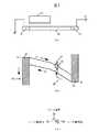
そこで、以下、この従来技術によるTFTの問題点について、図20により説明する。
この図20は、従来から使用されているnチヤネルTFTの断面図(a)と、キャリア捕獲準位がない(理想の)場合のポテンシャル図及び電流電圧特性図(b)、それに、キャリア捕獲準位がある(現実の)場合のポテンシャル図及び電流 電圧特性図(c)を示したものである。
【0011】
そして、このTFTは、図20(a)に示したように、n+ の高濃 度不純物注入領域221及びn- の低濃度不純物注入領域222で構成されるソース領域と、n+ の高濃度不純物注入領域223及びn- の低濃度不純物注入領域224から構成されるドレイン領域、iで示した不純物非注入領域225で構成されるチヤネル形成領域、それにゲート電極220で構成されている。
【0012】
従って、このTFTは、基本的にはMOSFET(絶縁ゲート型電界効果トランジスタ)で構成されていることになる。
なお、ここで不純物非注入領域に付されているiは、いわゆる真性半導体を意味する。
また、この図20では、ゲート電極220とi不純物非注入領域225の間にある絶縁層や、他の領域に形成される絶縁物については、簡略化のため省略して示してある。
【0013】
次に、この従来のTFTの動作について説明する。
始めに、説明の都合上、従来のTFTとは異なるが、チヤネル形成領域225にチヤネルキャリア捕獲準位が存在していない、理想的な場合のTFTを想定して、その動作について説明する。
【0014】
まず、図20のポテンシャル図(b)に示すように、チヤネル形成領域225にチャネルキャリア捕獲準位が存在しない理想的な場合には、ソース226から注さ入れた電子e- は、図示のように、チヤネル228に沿ってドレイン227へと拡散して、又はドリフトして移動し、チヤネル電流を形成する。
【0015】
この場合のゲート電圧Vgs に対するチヤネル電流Ids 特性を図20(b)の右に示す。
この図の中で、チヤネルに寄生容量がない場合は、矢印を付して示したテーリング領域と呼ぶ領域部分では、理論限界として、60mV/桁電流値特性を有する(kT/q・ln 10=60mV、但し、kはボルツマン定数、Tは温度、qは単位電荷量)。
【0016】
これは、例えば5桁の電流値を制御するのに必要なゲート電圧の振幅が300mVで済むことを意味する。
なお、この図20(b)、(c)では、説明の本質には影響はないので、n+ で示す高濃度不純物注入領域とn- で示す低濃度不純物注入領域について、ポテンシャル図中では区別して表示していない。
【0017】
次に、チヤネル形成領域225にチヤネルキャリア捕獲準位が存在している、現実的な従来のTFTについて、その動作について説明する。
多結晶Siをチヤネル形成領域225に用いた従来のTFTの場合、現実問題として、そのチヤネル形成領域226には、結晶欠陥や粒界に起因するチヤネルキャリア捕獲準位が多数存在する。
【0018】
従って、図20(c)に示すように、これらの捕獲準位に捕獲されたチヤネルキャリア231は、チヤネル中にポテンシャル障壁230を多数形成してしまい、チヤネル電流の拡散やドリフトを阻害する。
【0019】
そして、これらのチヤネルキャリア捕獲準位は、Siのバンドギャップ中に存在するため、ゲート電圧が、より正方向に印加されるほど多数のチヤネルキャリアが捕獲され、更にポテンシャル障壁230を成長させることになる。
換言すれば、ゲートに正の電圧を加えれば加える程、TFTの閾値電圧Vth が上昇してしまうことになる。
【0020】
この結果、図20(c)の右のゲート電圧Vgs 対チヤネル電流Ids 特性に示すように、矢印が付してあるテーリング領域部分は、同図(b)に示したチヤネルキャリア捕獲準位が存在しない理想的な場合と比較して大きく寝てしまい、その傾きは200mV/桁電流から300mV/桁電流以上にもなってしまう。
ここで、いま、300mV/桁電流の場合、これは例えば5桁の電流制御に必要なゲート電圧振幅が1500mV必要になるということを意味する。
【0021】
更に、実際にチヤネルキャリア捕獲準位が存在する現実的な場合には、ポテンシャル障壁230の成長によって、見かけ上の閾値電圧Vth が上昇するため、同じゲート電圧に対応するチヤネル電流値そのものも大きく減ってしまい、回路の駆動に必要となる駆動電圧は遥かに大きくなってしまう。
【0022】
現実問題として、多結晶Siをチヤネル形成領域225に用いた従来のTFTでは、安定動作には、一般に10Vから15V前後の駆動電圧が必要になり、このようにTFTの動作電圧が高くなってしまうため、従来技術では、低電圧駆動による消費電力の削減が困難であったのである。
なお、上記の議論は、nチヤネルのTFTを例にしたが、pチヤネルTFTでも同様である。
【0023】
本発明の一方の目的は、低電圧で充分に動作する電界効果トランジスタを提供することにある。
次に、本発明の他方2の目的は、消費電力が少なくて済む液晶表示装置を提供することにある。
【0024】
【課題を解決するための手段】
前記目的は、第1と第2のソース領域に挟まれたチャネル領域にゲート電極を有する絶縁ゲート型の電界効果トランジスタにおいて、前記チャネル領域は、平面形状が略カタカナのエの字状をした多結晶シリコン膜により形成され、前記第1のソース領域は、一方の導電型の半導体からなり、前記エの字状の上側になる方の辺の一方の端部に形成され、前記第2のソース領域は、前記一方の導電型とは別の他方の導電型の半導体からなり、前記エの字状の上側になる方の辺の他方の端部に形成され、前記エの字状の下側になる方の辺の一方の端部には、他方の導電型の半導体からなる前記第2のソース領域とは別の第2のソース領域が形成され、前記エの字状の下側になる方の辺の他方の端部には、一方の導電型の半導体からなる前記第1のソース領域とは別の第1のソース領域が形成され、前記ゲート電極を、前記チャネル領域の前記エの字状の上側になる方の辺の前記第2のソース領域の近傍の部分と前記チャネル領域の前記エの字状の下側になる方の辺の前記第2のソース領域とは別の第2のソース領域の近傍の部分を残して、前記チャネル領域の前記エの字状の上側になる方の辺と下側になる方の辺を結ぶ領域に共通に平面的に重ね合わせて形成することにより、前記上側になる方の辺のチャネル領域と前記下側になる方のチャネル領域のそれぞれで2個の電界効果トランジスタが形成されているようにして達成される。
【0026】
また、このとき、前記チャネル領域が真性半導体で形成されているようにしてもよく、前記チャネル領域の前記ゲート電極と平面的に重ね合わされていない領域に1e-18/cm3 以下の不純物が注入されているようにしてもよい。
【0027】
或いは、このとき、前記ゲート電極が、前記チャネル領域を保持している基板に対して、当該チャネル領域の前記基板とは反対側に設けられているようにしてもよく、前記ゲート電極が、前記チャネル領域を保持している基板に対して、当該チャネル領域と前記基板の間に設けられているようにしてもよい。
【0028】
更に、このとき、前記ゲート電極は、その少なくとも一部が、前記第1と第2のソース領域の何れか一方に対しても、平面的に重ね合わされているようにしてもよい。
【0031】
このとき、前記チャネル領域の前記ゲート電極と平面的に重ね合わされた領域が真性半導体から構成され、前記チャネル領域の前記ゲート電極と平面的に重ね合わされていない領域には1e-18/cm3 以下の不純物が注入されているようにしても上記目的が達成される。
【0032】
このとき、前記チャネル領域が真性半導体で形成され、更には、前記チャネル領域に1e-18/cm3 以下の不純物が注入されているようにしてもよい。
【0034】
また、上記目的は、少なくとも複数の画素を有する表示部と、少なくとも表示信号の信号処理と前記表示部に対する表示信号の書込みを行う制御部を同一絶縁基板上に備えた画像表示装置において、前記制御部の少なくとも一部が、一方の導電型で形成された第1のソース領域と前記一方の導電型とは別の他方の導電型で形成された第2のソース領域に挟まれたチャネル領域にゲート電極を有する絶縁ゲート型の電界効果トランジスタであって、前記チャネル領域を多結晶シリコン膜により形成し、前記チャネル領域に前記ゲート電極を平面的に重ね合わせる際、当該チャネル領域に前記ゲート電極が重ね合わされない領域を設け、当該ゲート電極が重ね合わされない領域の長さを、当該チャネル領域を構成する多結晶シリコンの結晶粒径よりも長く設定した電界効果トランジスタにより構成され、前記表示部の画素制御素子が、請求項1と請求項2に記載の電界効果トランジスタの何れかで構成されているようにしても達成される。
【0035】
【発明の実施の形態】
以下、本発明による電界効果トランジスタと液晶表示装置について、図示の実施の形態により、詳細に説明する。
<第1の実施形態>
まず、図1〜図9により、本発明の第1の実施形態について説明する。
この実施形態に係る多結晶シリコン(poly-Si)TFT液晶表示パネルは、図2に示すように、ガラス基板14を備え、このガラス基板14の上に、液晶容量4を有する画素1がマトリクス状に配置されている(図面の簡略化のため、画素1は4個だけ記載した)。
【0036】
そして、各画素1の液晶容量4は、ゲートが共通にゲート線5に接続され、ソースとドレインが直列接続された2個の画素TFT2、3を介して、信号線9に接続されている。
次に、各々の画素1は、まず行方向にゲート線5で並列に接続され、このゲート線5からゲート線バッファ8、ゲート線レベルシフタ7を介してゲート線シフトレジスタ6に接続されている。
【0037】
一方、列方向では、信号線9に並列に接続され、この信号線9から信号線スイッチ10を介して信号入力線12に接続されている。
このとき、信号線スイッチ10は、シフトレジスタ出力線11を介して、信号線シフトレジスタ13により制御される。
【0038】
次に、この実施形態の動作について説明する。
まず、信号線シフトレジスタ13は、シフトレジスタ出力線11を介して信号線スイッチ10を走査し、信号入力線12から入力された信号電圧を所定の信号線9に振り分ける。
【0039】
一方、ゲート線シフトレジスタ6は、ゲート線レベルシフタ7とゲート線バッファ8を介してゲート線5を順次走査し、所定の画素行の画素TFT2、3を開閉させ、信号線9に出力されている信号電圧を、画素1内の液晶容量4に印加する。
【0040】
そこで、この液晶容量4に入力された信号電圧が各画素1に対応する液晶部分の光学特性を変調し、この結果、表示パネル全体として、入力された信号電圧に応じた画像が表示されることになる。
【0041】
また、このとき、各画素に光学的反射電極を配置することにより、バックライトやフロントライトなどによる内部照明が無くても、外部環境光だけで画像表示が得られるようにした、いわゆる反射表示型の液晶表示装置として実施することができる。
【0042】
ここで、この実施形態によれば、駆動電圧が、例えば5Vと低くでき、この結果、消費電力が大幅に低減できるが、その理由は、ゲート線シフトレジスタ6、ゲート線レベルシフタ7、信号線シフトレジスタ13、それに信号線スイッチ10などに、以下に説明する低電圧駆動電界効果トランジスタが採用されているからである。
【0043】
図1は、本発明による低電圧駆動電界効果トランジスタの一実施形態を示したもので、この低電圧駆動電界効果トランジスタは、まず、図1(a)の断面図に示したように、n+ の高濃度不純物注入領域22で構成されている第1ソース領域と、p+ の高濃度不純物注入領域23で構成される第2ソース領域、iで示した不純物非注入領域24で構成されるチヤネル形成領域、それにゲート電極20で構成されている。
【0044】
但し、ここでも、ゲート電極20とi領域24の間、それに他の領域に形成される絶縁物(例えばSi O2 とSi3 N4)と、これらの下に設けられているガラス基板14は、図面の簡略化のために省略してある。
【0045】
そして、この低電圧駆動電界効果トランジスタでは、図1(b)の平面図に示すように、ゲート電極20が、i不純物非注入領域24の全領域に平面的に重ね合わされるようにして設けられているのではなくて、図示のように、n+ 高濃度不純物注入領域22に接している方の端部に偏って、i不純物非注入領域24の略半分の領域にだけ平面的に重畳した形で設けられている。
【0046】
更に、第1ソース領域となるn+ 高濃度不純物注入領域22には、一方のソース端子(1)が接続され、第1ソース領域となるp+ 高濃度不純物注入領域23には、他方のソース端子(2)が接続されている。ここで、これらのソース領域は、使用態様に応じて、何れか一方は、いわゆるドレイン領域となるものである。
【0047】
このとき、ゲート電極20の幅はi不純物非注入領域24の長さの略半分で、p+ 高濃度不純物注入領域23から約4μm離れた状態にしてあり、n+ 高濃度不純物注入領域22とp+ 高濃度不純物注入領域23、それにi不純物非注入領域24は、いずれも多結晶Si薄膜で形成されているが、更に、i不純物非注入領域24は、結晶粒径約0.5μm、膜厚50nmの多結晶Si薄膜になっている。
【0048】
ここで、上記の構成から明らかなように、この実施形態による低電圧駆動電界効果トランジスタも、従来の多結晶SiTFTと共通のプロセスにより容易に作成することができ、従って、従来の多結晶SiTFTと同一の基板上に作り分けることも容易である。
【0049】
次に、この実施形態に係る低電圧駆動電界効果トランジスタの動作について、図3により説明する。
まず、図3(a)に示すように、ソース端子(1)が接続されているn+ 高濃度不純物注入領域22を接地し、ソース端子(2)が接続されているp+ 高濃度不純物注入領域23を電圧Vh に接続したとすると、n+ 高濃度不純物注入領域22からi不純物非注入領域24にチヤネルキャリアである電子が注入される。
【0050】
ここで、この実施形態でも、チヤネル形成領域となるi不純物非注入領域24が、従来技術の場合と同じく、多結晶Siで作られており、このため、チヤネル形成領域には結晶欠陥や粒界に起因するチヤネルキャリア捕獲準位が多数存在する。
【0051】
従って、i不純物非注入領域24の中に注入されたチヤネルキャリアである電子e- は、図3(b)に示すように、捕獲準位に容易に捕獲されてしまう。
そして、捕獲準位に捕獲された電子25は、ゲート電極20の下も含めてi不純物非注入領域24の中にポテンシャル障壁30を多数形成してしまう。
【0052】
しかし、このとき、注入された電子の一部は、n+ 高濃度不純物注入領域22からゲート電極20の右端まで到達し、この部分のポテンシャルを低下させるので、ソース端子(2)が接続されているp+ 高濃度不純物注入領域23からのホールh+ の注入を誘起する。
【0053】
ここで、新規に注入されたホール26から見た場合、電子e- を捕獲した捕獲準位は負に帯電しているため、その捕獲断面積(capture crossection)が非常に大きくなり、この結果、極めて寿命の短い再結合中心として機能する。
【0054】
しかも、この再結合中心の寿命は、電子単体による捕獲準位の寿命よりも遥かに短く、このため、電子から見た場合のチヤネルキャリア捕獲準位はスクリーニングされてしまい、この結果、電子を捕獲したチヤネルキャリア捕獲準位25が生成するポテンシャル障壁30は、等価的には消滅してしまったものと看做すことができる。
【0055】
ここで、チヤネルキャリア捕獲準位は、新規に注入されたホールに対しても同様にキャリア捕獲を行うものの、この場合も、ホールを捕獲した捕獲準位は正に帯電しているため、その捕獲断面積が非常に大きく、極めて寿命の短い再結合中心として機能する。
【0056】
従って、ホールから見た場合のチヤネルキャリア捕獲準位も、同様のメカニズムでスクリーニングされてしまい、ホールを捕獲したチヤネルキャリア捕獲準位が生成するポテンシャル障壁も、同じく等価的に消滅してしまったものと見なすことができる。
【0057】
以上の結果、図1と図3に示した低電圧駆動電界効果トランジスタによれば、結晶欠陥や粒界に起因するチヤネルキャリア捕獲準位と、これに起因するポテンシャル障壁30の影響が回避できることが判る。
【0058】
また、この低電圧駆動電界効果トランジスタでは、電子とホールが相互にチヤネルキャリア捕獲準位に起因するポテンシャル障壁をスクリーニングするため、i不純物非注入領域24に寄生する抵抗の影響も殆どなく、無視できることも判る。
【0059】
従って、この実施形態に係る低電圧駆動電界効果トランジスタでは、ゲート電圧Vgs に対するチヤネル電流Ids 特性として、100mV/桁電流以下の値の特性のものが容易に得られることになる。
【0060】
また、この実施形態においては、従来技術とは異なり、ゲート電圧を上げた際にもポテンシャル障壁30の成長に起因する閾値電圧Vth の増大も起こらないので、5Vの低電圧による駆動で、充分な出力電流が確保できる。
【0061】
次に、本発明による低電圧駆動電界効果トランジスタの他の実施形態について説明する。
ここで、これ以降での説明を容易にするため、本発明による低電圧駆動電界効果トランジスタを“両極性TFT”と称することとし、更に、この両極性TFTについては、ここでは図3(c)に示す記号で表現することとする。
なお、これは、n+ とp+ の両極性のソースを有するという、この電界効果トランジスタの特徴に由来する。
【0062】
ところで、この図3に示した両極性TFTの実施形態は、その低電圧側端子であるソース端子(1)の電圧を基準にし、これに対してゲート端子からゲート電極20に印加された電圧の大きさによりチヤネル電流が制御されるものである。
【0063】
しかし、本発明によれば、反対に、高電圧側端子であるソース端子(2)に対するゲート端子印加電圧によって、そのチヤネル電流を制御するようにした両極性TFTも、類似の構成により実現することができ、以下、これを本発明の第2の実施形態として、図4を用いて説明する。
【0064】
この第2の実施形態による両極性TFTは、図4(a)の断面図と同図(b)の平面図に示すように、n+ 高濃度不純物注入領域22pからなる第3ソース領域と、p+ 高濃度不純物注入領域23pからなる第4ソース領域、それに、i不純物非注入領域24pからなるチヤネル形成領域、それにゲート電極20pで構成されている。
【0065】
そして、n+ 高濃度不純物注入領域22pからなる第3ソース領域にはソース端子(3)が接続され、p+ 高濃度不純物注入領域23pからなる第4ソース領域にはソース端子(4)が接続されている。
なお、ここでも、ゲート電極20pとi領域24pの間と、その他の領域に形成されている絶縁物(Si O2 とSi3 N4 )は、図面の簡略化のために省略している。
【0066】
ここで、この第2の実施形態に係る両極性TFTが、図1で説明した実施形態と大きく異なる点は、i不純物非注入領域24pからなるチヤネル形成領域に対するゲート電極20pの重ね合わせ位置が反対になっている点にある。
【0067】
すなわち、図示のように、この実施形態では、i不純物非注入領域24のp+ 高濃度不純物注入領域23pからなる第4ソース領域に接している方の端部に偏って、略半分の領域にだけ重畳した形でゲート電極20p設けられているのである。
【0068】
このときも、ゲート電極20pは、ソース端子3を有するn+ 高濃度不純物注入領域22pから約4μm離れている。
そして、この第2実施形態による両極性TFTについては、ここでは図4(c)に示す記号で表現することとする。
また、便宜上、これ以降は、図3で説明した両極性TFTを「nチヤネル」、第2の両極性TFTを「pチヤネル」と表現することにする。
【0069】
この図4に示す第2の実施形態による両極性TFTの動作に関しては、n+ 領域とp+ 領域、及び電子とホールを入替え、ポテンシャルの上下を逆にすれば、図3で説明した両極性TFTの動作と同様であるため、ここでは、説明は省略する。
【0070】
次に、本発明の更に別の実施形態について説明する。
図5は、図2の実施形態におけるゲート線シフトレジスタ6と信号緑シフトレジスタ13に用いられているシフトレジスタ単位ユニットの構成図である。
このシフトレジスタ単位ユニットの入力端子30は、第1クロックck1により制御されるクロックトインバータ31の入力に接続される。ここで、クロックトインバータとは、クロックで動作制御されるインバータ(反転回路)のことである。
【0071】
そして、このクロックトインバータ31の出力は、インバータ32及び第2クロックck2で制御されるクロックトインバータ33で構成される第1のフリップフロツプに入力され、更に、この第1のフリップフロップの出力は、第1のシフトレジスタ出力34と、クロックck2で制御されるクロックトインバータ36の双方に接続される。
【0072】
クロックトインバータ36の出力は、インパーク37及びクロックck1で制御されるクロックトインバータ38で構成される第2のフリップフロップに入力され、この第2のフリップフロップの出力は、第2のシフトレジスタ出力39とシフトレジスタ単位ユニットの出力端子40の双方に接続される。
ここで、クロックck1とクロックck2とは、互いに“H”と“L”が反転した相補クロックである。
【0073】
次に、このシフトレジスタ単位ユニットの動作について説明すると、これは基本的には従来から知られているものと同じである。
すなわち、第1クロックck1で制御されるクロックトインバータ31がオンになることで、前段のシフトレジスタ単位ユニットからの出力を第1のフリップフロップに取込み、第2クロックck2で制御されるクロックトインバータ36がオンになることで、第1のフリップフロツプの信号を第2のフリップフロップに取込むというシフト動作を繰り返すのである。
【0074】
しかし、この図5の実施形態では、従来技術と異なり、各クロックトインバータとインバータに、本発明に係る両極性TFTが用いられているので、5V以下の低電圧でも容易に動作させることができ、これが、この実施形態の大きな特徴である。
【0075】
以下、これらの回路に関して説明する。
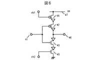
まず、図6は、本発明の実施形態によるクロックトインバータ33、36の構成図で、これらは、図示のように、2個のpチヤネル両極性TFT44、42と2個のnチヤネル両極性TFT43、45を、高電圧電源(VH)47と接地電位の間に、高電圧側から低電圧側に電流を流す極性で、接続したものである。
【0076】
そして、入力端子41は、pチヤネル両極性TFT42とnチヤネル両極性TFT43の双方のゲートに共通に接続され、pチヤネル両極性TFT42とnチヤネル両極性TFT43の双方のソース端子に共通に出力端子46が設けられている。
【0077】
その上で、第1クロックck1は、pチヤネル両極性TFT44のゲートに供給され、第2クロックck2は、nチヤネル両極性TFT45のゲートに供給される。
従って、まず、第1クロックck1が“H”で、第2クロックck2が“L”のとき、pチヤネル両極性TFT44とnチヤネル両極性TFT45が共にオフされ、両ソース電極間が開放状態になるので、出力端子46は開放となる。
【0078】
次に、第1クロック1ck1が“L”になって、第2クロックck2が“H”になると、pチヤネル両極性TFT44とnチヤネル両極性TFT45は共にオンされ、両ソース電極間が短絡状態になる。
この場合、入力端子41に“H”が入力されたとすると、nチヤネル両極性TFT43は短絡、pチヤネル両極性TFT42は開放になる。
【0079】
従って、出力端子46には“L”が現われ、入力端子41に“L”が入力されたとすれば、今度はnチヤネル両極性TFT43は開放で、pチヤネル両極性TFT42は短絡になるため、出力端子46には“H”が現れることになり、クロックトインバータとして動作することになる。
【0080】
ここで、クロックのレベル“L”、“H”での各出力電圧は、それぞれ接地電圧と高電圧電源(VH)47電圧で決まり、従って、これはCMOSクロックトインバータの動作に相当する。
ちなみに、この実施形態においては、高電圧電源(VH)47の電圧は5Vで充分であった。
【0081】
ところで、この図6では、クロックトインバータ33、36について説明したが、クロックトインバータ31、38については、第1クロックck1と第2クロックck2を入れ替えたものであり、従って、ここでは説明は省略する。
【0082】
次に、図7は、インバータ32、37の構成図で、これらは、図示のように、pチヤネル両極性TFT49とnチヤネル両極性TFT50の2個の両極性TFTを、高電圧電源(VH)47と接地電位の間に、高電圧側から低電圧側に電流を流す極性で、接続したものである。
【0083】
そして、入力端子48は、pチヤネル両極性TFT48とnチヤネル両極性TFT50の双方のゲートに共通に接続され、pチヤネル両極性TFT48とnチヤネル両極性TFT50の双方のソース端子に共通に出力端子51を設けたものである。
【0084】
次に、この図7の実施形態の動作について説明する。
いま、ここで、入力端子48に“H”が入力されたとすると、nチヤネル両極性TFT50は短絡、pチヤネル両極性TFT49は開放になり、このため出力端子51は“L”になる。
【0085】
また、入力端子48に“L”が入力された場合には、今度はnチヤネル両極性TFT50は開放、pチヤネル両極性TFT49は短絡になるため、出力端子51には“H”が現れることになり、インバータ、つまり反転回路として動作することになる。
【0086】
なお、ここでも、出力“L”と出力“H”での電圧は、それぞれ接地電圧と、高電圧電源(VH)47の電圧で決まるので、これはCMOSインバータの動作に相当する。
ちなみに、ここでも、高電圧電源(VH)47の電圧は5Vとしても充分に動作することは、既に述べた通りである。
【0087】
ところで、上記の説明においては、“両極性TFTが短絡する”という表現を用いたが、これは、正確には若干異なる。すなわち、両極性TFTがオンした場合は、p+ 高濃度不純物領域とn+ 高濃度不純物領域が、iチャネル形成領域を挟んで順方向導通されることになると考えて良いが、この場合、その電流電圧特性がダイオード特性に近似されるからである。
【0088】
このとき、近似されるダイオードの逆方向リーク電流が小さい場合は、両極性TFTの両端の電圧が等しいときのオン抵抗は大きくなり、逆方向リーク電流が大きい場合には、両極性TFTの両端の電圧が等しいときのオン抵抗は小さくなる。
【0089】
現実には、上記実施形態のように、4μm幅のチャネル形成領域を挟んだダイオードの場合、逆方向リーク電流は1PA/μm以下と小さいため、両極性TFTの両端の電圧が等しい場合のオン抵抗は大きく、実際の回路出力には0.5V程度の出力オフセット電圧が入ると考えて良い。
【0090】
このため、この実施形態においては、nチヤネル両極性のソース端子(1)とゲート間電圧、及びpチヤネル両極性TFTのソース端子(4)とゲート間で規定される閾値電圧Vth を、上記の出力オフセット電圧より大きい1.5Vと−1.5Vの電圧になるように作り、次段の両極性TFTが充分に余裕を持ってオフされるようにしている。
【0091】
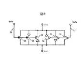
次に、図2の実施形態における信号線スイッチ10の実施形態について、図8により説明する。
ここで、まず、この図8でVin とVout で示してある信号線スイッチ10の両端子の間には、図示のように、nチヤネルTFT58とnチヤネル両極性TFT52、53がそれぞれ逆向きに接続されており、これらのゲート電極には信号線スイッチ正ゲート線56が共通に接続されている。
【0092】
また、更にこれらと並列に、pチヤネルTFT59とpチヤネル両極性TFT54、55がそれぞれ逆向きに接続されており、これらのゲート電極には信号線スイッチ逆ゲート線57が接続されている。
次に、この図9の実施形態の動作について説明する。
【0093】
信号線スイッチ正ゲート線56と信号線スイッチ逆ゲート線57には、それぞれがレベル反転している“H1”と“L1”の信号が印加されるが、これらの信号電圧の内、一方の“H1”の電圧は、入力Vinと出力Vout 間に現れる電圧よりも高い電圧になるようにしてあり、他方、信号電圧“L1”は、入力Vinと出力Vout 間に現れる電圧よりも低い電圧になるようにしてある。
【0094】
そこで、いま、信号線スイッチ正ゲート線56に“L1”、信号線スイッチ逆ゲート線57に“H1”が入力されたとすると、この場合は、上記した全てのトランジスタはオフ状態になり、従って、入力Vinと出力Vout 間は開放されたままで、オフになる。
【0095】
これに対して、信号線スイッチ正ゲート線56に“H1”、信号線スイッチ逆ゲート線57には“L1”が入力されたとすると、この場合は、上記全てのトランジスタは、今度はオン状態になり、従って、入力Vin と出力Vout 間は短絡状態になる。
従って、この図8の構成により、スイッチ機能が得られ、信号線スイッチ10を実現することができる。
【0096】
ここで、この実施形態では、6個のトランジスタが使用されているが、これらはそれぞれ異なる役割を果たす。
まず、pチヤネルとnチヤネルの各トランジスタは、入力Vin と出力Vout 間の電圧が高い場合と低い場合に、それそれ分けて機能する。次に、接続方向が異なる両極性TFTは、それぞれ異なる向きの電流駆動を行う。
【0097】
このとき、両極性TFTは、両端のソース電圧が1V以上異なる場合には、大きな電流駆動能力を示すが、両端のソース電圧がほぼ等しい状態では、抵抗が大きくなってしまうことは既に説明した通りである。
【0098】
そこで、図8に示すように、普通のTFT58、59を各々並列に接続し、信号線スイッチ10の書込み初期(導通立上り時期)には両極性TFTが支配的に電流を駆動し、書込み終了近く(導通完了時期)になって入力Vin と出力Vout 間の電圧が近づくにつれ、普通のTFTが支配的に電流を駆動するように構成したのである。
【0099】
次に、図2の実施形態におけるゲート線レベルシフタ7の実施形態について、図9により説明する。
まず、pチヤネルTFT68、66と、nチヤネル両極性TFT65からなる入力信号反転回路を、電圧VHHが印加された電源線69と接地電位の間に直列に接続し、pチヤネルTFT67、64、nチヤネル両極性TFT63からなる入力信号反転回路も、同じく電圧VHHが印加された電源線69と接地電位の間に直列に接続する。
【0100】
そして、pチヤネルTFTとnチヤネル両極性TFT65の接続点と、pチヤネルTFT64とnチヤネル両極性TFT63の接続点を各入力信号反転回路の出力端子71、72とする。
また、これらの出力端子71、72は、それぞれpチヤネルTFT67、68のゲートに接続してある。
【0101】
次に、pチヤネルTFT66とnチヤネル両極性TFT65のゲートは、それぞれ逆入力端子62に共通に接続され、pチヤネルTFT64とnチヤネル両極性TFT63のゲートは、それぞれ正人力端子61に共通に接続されている。
【0102】
次に、この図9の実施形態の動作について説明する。
このゲート線レベルシフタ7には、正人力端子61と逆入力端子62から、それぞれ相互にレベルが反転した“H”と“L”の信号が入力され、これにより、2組の入力信号反転回路がそれぞれ逆の信号を出力する。
【0103】
ここで、まず一方の入力信号反転回路のnチヤネル両極性TFTがオンのときは、その回路の出力は0Vであり、この0Vが他方の入力信号反転回路のpチヤネルTFTをオンさせるため、他方の回路の出力は電圧VHHになる。
【0104】
このとき、この実施形態では、正入力端子61と逆入力端子62に供給される信号の電圧は5Vで、電源電源VHHは10Vに設定してあり、従って、レベルシフタとして動作することになる。
そして、この実施形態の場合、nチヤネル両極性TFT63、65の電流立上がり特性が良好で急峻になっているため、5Vの低い電源電圧でゲート線レベルシフタ7を動作させることができる。
【0105】
なお、この図9において、他のpチヤネルTFTも両極性TFTに置き換えることもできるが、低電圧駆動が5Vの場合は、そこまでする必要はなく、一方、pチヤネルTFTを用いた方が出力振幅が最大VHHまで大きく取れるという利点が得られる。
【0106】
ここで、回路規模の増加を許すならば、pチヤネルTFTにも並列にpチヤネル両極性TFTを設ける方法を採用することによって、出力振幅をフルスイングさせながら、出力電流を向上させることも可能であることは、図8に説明した信号線スイッチ10で説明したことからも明らかである。
【0107】
ところで、これまで説明した両極性TFTでは、上記したように、ゲート端子からソース端子(2)まで、或いはソース端子(3)までのi領域の幅(電流経路の長さ)が4μmに設定してあるが、このi領域の幅は、それが狭い方が出力電流は大きくなり、また両電流端子間の電圧が近づいた際の順方向ダイオードモードにおける出力抵抗も低減できる。
【0108】
しかしながら、このi領域の幅が、多結晶Siの結晶粒径より狭くなってしまうと、結晶粒界準位の影響が見えなくなるため、ゲート電極の電圧を正/負のいずれに振っても電流をオフすることのできず、この結果、単にnチヤネルTFTとpチヤネルTFTが並列に接続されたTFTペアと同じになって、もはや両極性TFTとしての機能が失われてしまう。
【0109】
従って、両極性TFTのオフ特性は、このi領域の幅で決ってしまうので、その幅は、製造上のインアラマスクの合わせずれ等のばらつきを考慮して上で、慎重に決定されなくてはならないが、ここで、現実のTFTプロセスを考慮した場合、このi領域の幅は、1μmから6μm程度が適当な値と考えられる。
【0110】
なお、上記実施形態では、両極性TFTにおけるゲート電極下及びゲートに隣接するチヤネル形成領域がi領域の場合について説明したが、ここで、このi領域これに1e-18/cm3 以下の微量の不純物を入れておくことにより、両極性TFTの閾値電圧Vth を制御することもできる。
【0111】
但し、このことは、従来のTFTにおいて、閾値電圧Vth の制御に適用されている一般的な技術であり、従って、上記のことは、従来技術を両極性TFTにも適用したことに相当する。
【0112】
ところで、以上の実施形態では、両極性TFTを、図2の実施形態における画素TFT2、3に適用した例について説明しなかったのは、上記した“i領域”の空乏化部分が光感度を有し、これによる光電変換電流がオフリーク電流となってしまうためであり、従って、上記実施形態において、両極性TFTを含む周辺回路部分は、入射光に起因する誤動作に対する余裕を確保するため、遮光しておくのが望ましい。
【0113】
ここで、以上に説明した実施形態については、本発明の主旨を損なわない範囲でいくつもの変更が可能である。
例えば、上記実施形態では、パネルの基板として、ガラス基板14を用いているが、これを石英基板や透明プラスチック基板に変更することも可能であるし、更に反射型表示の場合には、不透明な基板を用いることも可能である。
【0114】
また、上記実施形態の説明では、画素数やパネルサイズ等に関しては敢えて言及していない。
これは、本発明の実施形態が、特にこれらのスペック乃至フォーマットに制限されるものではないためである。
【0115】
更に、上記実施形態では、従来の普通のTFTと本発明による両極性TFTとを適宜使い分けているが、この使い分け方には種々の設計思想や設計仕様に基づく様々なバリエーションが存在することは言うまでもない。
【0116】
例えば、オン抵抗の仕様によっては、信号線スイッチ10は、従来のTFTのみで構成するなどの選択肢も存在する。
勿論、以上の種々の変更は、以上の実施形態に限らず、以下に説明する他の実施形態においても、基本的には同じであることは言うまでもない。
【0117】
<第2の実施形態>
次に、本発明の第2の実施形態について説明する。
図10は、第2の実施形態に係る多結晶シリコンTFT液晶表示パネルを示したもので、図示のように、この実施形態でも、図2で説明した第1の実施形態と同じく、ガラス基板14を備え、このガラス基板14の上に、液晶容量4を有する画素1がマトリクス状に配置されている(同じく簡略化のため、画素1は4個だけ記載した)。
【0118】
そして、各画素1の液晶容量4は、ゲートが共通にゲート線5に接続され、ソース−ドレインが直列接続された2個の画素TFT2、3を介して、信号線9に接続されている。
また、各画素1は、行方向にはゲート線5で並列に接続され、列方向では、信号線9に並列に接続されている。
そして、行方向のゲート線5は、ゲート線バッファ8、ゲート線レベルシフタ7を介してゲート線シフトレジスタ6に接続されている。
【0119】
従って、これまでの構成は、図2で説明した実施形態と同じで、ゲート線レベルシフタ7とゲート線バッファ8を介して、ゲート線シフトレジスタ6により、ゲート線5が順次走査され、これにより、信号線9に振り分けられた信号電圧を所定の画素1内の液晶容量4に印加し、これにより各画素1に対応する液晶部分の光学特性を変調し、この結果、表示パネル全体として、入力された信号電圧に応じた画像が表示されるように動作する点も、同じである。
【0120】
また、このとき、各画素に光学的反射電極を配置することにより、バックライトやフロントライトなどによる内部照明が無くても、外部環境光だけで画像表示が得られるようにした、いわゆる反射表示型の液晶表示装置として実施することができる点も、図2の実施形態と同じである。
【0121】
しかして、この図10の実施形態では、信号線9が信号線シフトレジスタ13に至るまでの回路構成が図2の実施形態とは異なっている。
そこで、以下、この図2の実施形態とは異なっている点に重点をおいて説明する。
【0122】
まず、この図10の実施形態では、各画素1から出た信号線9は、それぞれの電圧セレクタ87に接続されている。
一方、信号線シフトレジスタ13の出力は、1次ラツチ制御線89と共にNAND回路88の各入力に接続され、各NAND回路88の出力により、それぞれのデータ1次ラッチ82が制御される。
【0123】
ここで、データ入力線81には、4ビット並列のデジタルデータが入力され、これらのデータはデータ1次ラツチ82に入力された後、このデータ1次ラッチ82から出力され、2次ラツチ制御線83で制御されるデータ2次ラッチ84に供給される。そして、このデータ2次ラツチ84の出力が電圧セレクタ87に入力されるようになっている。
【0124】
一方、ラダー抵抗85からは16本の基準電圧線86が引き出され、これにより、各画素1の中にある液晶を16階調で変調するのに必要な16種類の基準電圧が電圧セレクタ87に入力されている。
次に、この実施形態の動作について説明する。
【0125】
信号線シフトレジスタ13の出力信号は、1次ラッチ制御線89の信号とAND論理がとられた上で各データ1次ラッチ82に供給され、これにより、4本のデジタルデータ入力線81から入力された4ビットのデジタル信号データを、所定のデータ1次ラツチ82に振り分けで取り込ませる。
【0126】
このデータ1次ラツチ82に振り分けられたデジタル信号データは、2次ラツチ制御線83から入力される信号により制御され、1水平走査周期で駆動される2次データラツチ84にラツチされ、電圧セレクタ87に入力される。
【0127】
ラダー抵抗85は、デコード後のアナログ電圧を16本の基準電圧線86を介して電圧セレクタ87に入力し、電圧セレクタ87はこの基準電圧を用いて4ビットのデジタル信号データのデコード処理(DA変換)を行う。
【0128】
なお、この電圧セレクタ87によるDA変換動作に関しては、例えば、
“ISSCC2000 Digest of technical papers,pp188-189(2000)"
に報告されているため、ここでは詳細な構成及び動作の説明は省略する。
このようにして、電圧セレクタ87からは、4ビットのデジタル信号データが所定のアナログ信号電圧に変換され、信号線9に出力される。
【0129】
一方、ゲート線シフトレジスタ6は、上記したように、ゲート線レベルシフタ7とゲート線バッファ8を介してゲート線5を順次走査し、所定の画素行の画素TFT2、3を開閉制御し、信号線9に出力されている信号電圧を、画素1内の液晶容量4に入力する。
【0130】
そこで、この液晶容量4に入力された信号電圧が各画素1に対応する液晶部分の光学特性を変調し、この結果、表示パネル全体として、入力された信号電圧に応じた画像が表示されることになる。
【0131】
また、このとき、各画素に光学的反射電極を配置することにより、バックライトやフロントライトなどによる内部照明が無くても、外部環境光だけで画像表示が得られるようにした、いわゆる反射表示型の液晶表示装置として実施することができる。
【0132】
そして、この図10の実施形態でも、ゲート線シフトレジスタ6、ゲート線レベルシフタ7、信号線シフトレジスタ13などには、図2の実施形態と同じく、部分的に両極性TFTを採用しており、従って、駆動電圧を、例えば5Vに低減しても充分に動作でき、消費電力を大幅に低減することができる。
【0133】
ここで、これらの回路の構成及び動作については、既に図2の実施形態において説明してあるので、ここでは省略し、以下、この図10の実施形態の特徴であるデータ1次ラッチ82と、データ2次ラッチ84の構成について説明する。
【0134】
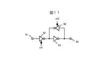
図11は、この実施形態におけるデータ1次ラッチ82及びデータ2次ラッチ84に用いられているラツチ単位ユニットの構成図で、このラッチ単位ユニットの入力端子91は、第1クロックck1により制御されるクロックトインバータ92の入力に接続されている。
【0135】
そして、このクロックトインバータ92の出力は、インバータ93と、第2クロックck2により制御されるクロックトインバータ94とで構成されるフリップフロップに入力され、このフリップフロップの出力がラッチ単位ユニットの出力端子95に接続されている。
このとき、第1クロックck1と第2クロックck2も、“H”と“L”が相互に反転した相補クロックである。
【0136】
次に、この図11のラツチ単位ユニットの動作について説明すると、これも、既に図5で説明したシフトレジスタ単位ユニットと、基本的には大きな違いはない。
すなわち、第1クロックck1で制御されるクロックトインバータ92がオンになることで、入力端子91の信号をフリップフロップに取込み、第2クロックck2で制御されるクロックトインバータ94がオンになることにより、このフリップフロップに取込まれた1ビットの信号データをラッチするのである。
【0137】
そして、この実施形態でも、各クロックトインバータと各インバータに両極性TFTを用いているため、特に5V以下の低電圧でも容易に動作させることができるという長所がある。
【0138】
ここで、この両極性TFTを用いた本ラツチ単位ユニットの構成及び動作に関しては、先に第1の実施形態において、図6と図7により説明したシフトレジスタ単位ユニットと同じであり、従って、ここでは、説明を省略する。
【0139】
次に、この図10の実施形態におけるNAND回路88の構成について、図12により説明する。
まず、このNAND回路88は、図12に示すように、2個の入力端子91、92と、1個の出力端子97を備えている。そして、入力端子91、92は、それぞれ電源電圧線45に一方のソース端子が接続されているpチヤネル両極性TFT93、94のゲートに接続されている。
【0140】
そして、これらのpチヤネル両極性TFT93、94の他方のソース端子は、直列に接続されている2個のnチヤネル両極性TFT96、95を介して、接地電位に接続されており、更に、nチヤネル両極性TFT96のゲートは入力端子91に、nチヤネル両極性TFT95のゲートは入力端子92に、それぞれ接続されている。
【0141】
ここで、pチヤネル両極性TFTは、論理回路としてはpMOSとして、nチヤネル両極性TFTは、論理回路としてはnMOSとして、それぞれほば同等の動作をする。
従って、このNAND回路88が、入力端子91、92のNAND論理が出力端子97に出力されることは明らかである。
ちなみに、この場合でも、電圧VHは5Vで、入力される論理電圧は5/0Vにしてある。
【0142】
ここで、このNAND回路88は、“H”の出力電圧は約4.5(5−0.5)Vで、“L”の出力電圧は1.0(0.5+0.5)V程度であり、このため、これの出力信号が入力するデータ1次ラッチ82の閾値は、nチヤネルが電圧1.5Vで、pチヤネルが電圧−1.0Vに設計してある。
【0143】
このように、両極性TFTの場合、その出力は、電源電圧一杯までの振幅特性を持たない。しかし、必要に応じて従来のTFTを並列に設ければ良いことは、第1の実施形態についての説明の中で既に説明した通りである。
【0144】
<第3の実施形態>
次に、本発明の第3の実施形態について説明する。
ここで、この第3の実施形態の場合、それに係る多結晶シリコンTFT液晶表示パネルの構成及び動作は、既に説明した第1の実施形態のそれとほば同じであるから、説明は省略し、ここでは、異なっている点について以下に説明する。
【0145】
図13は、この第3の実施形態において用いられている両極性TFTの構造図で、これは、第1の実施形態に関連して説明した図1(a)の断面図に相当するものである。
【0146】
そして、この図13に示すように、この第3の実施形態における両極性TFTは、n+ 高濃度不純物注入領域122(図1では22)からなる第1ソース領域、p+ 高濃度不純物注入領域123(同じく23)からなる第2ソース領域、i不純物非注入領域124(同じく24)からなるチヤネル形成領域、それにゲート電極120(同じく20)を備えている。
【0147】
従って、これらの点では、図1の実施形態と同じであるが、この第3の実施形態の場合は、更に上記の構成に加えて、チヤネル形成領域の中でゲート電極120と平面的に重畳していない部分に、n- 低濃度不純物注入領域126が設けられており、これが、図1の実施形態とは異なっている点である。
【0148】
ここで、このn- 低濃度不純物注入領域126は、1e-18/cm3 の濃度で、P(燐)を注入して形成されている。
そして、ゲート電極120は、一方のソースに相当するn+ 高濃度不純物注入領域122に接するようにして、i不純物非注入領域124と平面的に重畳しており、他方のソースに相当するp+ 高濃度不純物注入領域123からは約4μm離れている。
【0149】
なお、ここでも、ゲート電極120とi不純物非注入領域124の間と、その他の領域に形成されているSiO2とSi3 N4 などからなる絶縁物や下方のガラス基板14は省略してある。
【0150】
このようなn- 低濃度不純物注入領域126を導入することにより、この第3の実施形態に係る両極性TFTは更に高い電流駆動能力が与えられ、低電圧動作に対して大きな余裕を持つことになっている。
【0151】
このとき、n- 濃度不純物注入領域126の不純物濃度が1e-18/cm3 を大きく超えてしまうと、p+ 高濃度不純物注入領域123から注入されたホールの再結合速度が大きくなりすぎて、チヤネル形成領域内でのi不純物非注入領域124に注入されるホールの量が極めて小さくなってしまうので、望ましくない。
【0152】
何故なら、このとき両極性TFTは、あたかもn+p+ダイオードに接続された従来のTFTのようになってしまうからであり、このときは、チヤネル形成領域内に両極性のキャリアを注入することによる本発明の両極性TFT特有の効果が失われてしまうからである。
【0153】
なお、ここでも、nチヤネルの両極性TFTについてだけ説明したが、pチヤネルの両極性TFTについても、必要に応じて同様に、p- 低濃度不純物注入領域を用いることができ、更には、nチヤネルとpチヤネルの双方に対して、n- とp- の低濃度不純物注入領域を任意に組み合わせることが可能である。
【0154】
<第4の実施形態>
次に、本発明の第4の実施形態について説明する。
この第4の実施形態でも、それに係る多結晶シリコンTFT液晶表示パネルの構成及び動作は、既に説明した第1の実施形態のそれとほば同じであるから、説明は省略し、ここでは、異なっている点について以下に説明する。
【0155】
図14は、この第4の実施形態において用いられている両極性TFTの構造図で、これは、第1の実施形態に関連して説明した図1(a)の断面図に相当するものである。
【0156】
この図14に示した両極性TFTは、n+ 高濃度不純物注入領域132(図1では22)からなる第1ソース領域、p+ 高濃度不純物注入領域133(同じく23)からなる第2ソース領域、i不純物非注入領域134(同じく24)からなるチヤネル形成領域、それにゲート電極130(同じく20)を備えている。
【0157】
従って、これらの点では、図1の実施形態と同じであるが、この第4の実施形態の場合は、ゲート電極130がi不純物非注入領域134とi不純物非注入領域134とガラス基板14の間に形成されている点で、図1に示した第1の実施形態とは異なっている。
【0158】
そして、ゲート電極120は、i不純物非注入領域134だけではなく、一方のソースに相当するn+ 高濃度不純物注入領域132にも、一部が平面的に重畳するようにして重ね合わされており、他方のソースに相当するp+ 高濃度不純物注入領域133からは約4μm離れている。
【0159】
なお、ここでも、ゲート電極130とn+ 高濃度不純物注入領域132及びi不純物非注入領域134の間、それに、その他の領域に形成されているSiO2とSi3 N4 などからなる絶縁物は省略してある。
【0160】
ここで、ゲート電極がチヤネル形成領域とガラス基板の間に挟まれている構造は、いわゆる逆スタガ構造と呼ばれ、図示されていないが、この実施形態では、そこに、この図14に示した両極性TFTと一緒に使用されている普通のTFTがあった場合、製造プロセス上の共通化を図るため、この両極性TFTと同様、普通のTFTについても、ゲート電極がチヤネル形成領域とガラス基板の間に挟まれた逆スタガ構造が採用されている。
【0161】
そして、この場合、普通のTFTに加えて両極性TFTの構造も逆スタガ構造に整合させたため、従来のアモルフアスSi−TFTのデバイス構造と類似のプロセスラインにより容易に製造することができるという利点を有する。
【0162】
従って、この第4の実施形態によれば、既存のアモルフアスSi−TFTの製造ラインに大幅な変更を施すことなく、容易に多結晶シリコンTFT液晶表示パネルを製造することができるという利点がある。
【0163】
なお、この第4の実施形態に係る両極性TFTの場合、n+ 高濃度不純物注入領域132をゲート電極130と自己整合構造で作成するためには、ガラス基板14の裏面からの露光プロセスが新規に必要になってしまう。
【0164】
そこで、この図14の実施形態では、従来のアモルフアスSi−TFTの製造工程からの大幅な変更を回避するため、n+ 高濃度不純物注入領域132については、レジストマスク合わせを用いたイオンインプラフロセスで形成した。
【0165】
この場合、n+ 高濃度不純物注入領域132とゲート電極130間のオフセットを回避する必要があり、このため、この実施形態では、上記したように、n+ 高濃度不純物注入領域132を、ゲート電極130に対して平面的には重なるように形成したのである。
【0166】
なお、ここでも、nチヤネルの両極性TFTについてだけ説明したが、pチヤネルの両極性TFTについても、必要に応じて同様に、p- 低濃度不純物注入領域を用いることができ、更には、nチヤネルとpチヤネルの双方に対して、n- とp- の低濃度不純物注入領域を任意に組み合わせることが可能である。
【0167】
<第5の実施形態>
次に、本発明の第5の実施形態について説明する。
この第5の実施形態でも、それに係る多結晶シリコンTFT液晶表示パネルの構成及び動作は、既に説明した第1の実施形態のそれとほば同じであるから、説明は省略し、ここでは、異なっている点について以下に説明する。
【0168】
図15は、この第5の実施形態において用いられている両極性TFTの構造図で、これは、第1の実施形態に関連して説明した図1(a)の断面図に相当するものである。
【0169】
この図15に示した両極性TFTは、n+ 高濃度不純物注入領域142(図1では22)からなる第1ソース領域、p+ 高濃度不純物注入領域143(同じく23)からなる第2ソース領域、i不純物非注入領域144(同じく24)からなるチヤネル形成領域、それにゲート電極140(同じく20)を備えている。
【0170】
従って、これらの点では、図1の実施形態と同じであるが、この第4の実施形態の場合は、ゲート電極がゲート電極140、141の2個設けてある点で、第1の実施形態とは大きく異なっている。
【0171】
ここで、一方のゲート電極140は、一方のソースを形成しているn+ 高濃度不純物注入領域142側に接しており、他方のゲート電極141は、p+ 高濃度不純物注入領域143側に接している。
【0172】
なお、ここでも、ゲート電極140、141とn+ 高濃度不純物注入領域142とp+ 高濃度不純物注入領域143、それにi不純物非注入領域144の間、及びその他の領域に形成されているSiO2とSi3 N4 などからなる絶縁物や下方のガラス基板14は省略してある。
【0173】
ここで、この図15の実施形態に係る両極性TFTの場合、ゲート電極140がn+ 高濃度不純物注入領域142よりも高電位にされ、且つ、ゲート電極141がp+ 高濃度不純物注入領域143よりも低電位にされたときだけ導通する。何故なら、この両極性TFTの動作には両極性キャリアの注入が必要だからである。
【0174】
そして、この図15の実施形態に係る両極性TFTの場合、ゲート電極140がn+ 高濃度不純物注入領域142よりも高電位にされるとチヤネル形成領域144には電子が注入され、ゲート電極141がp+ 高濃度不純物注入領域143よりも低電位にされたとき、チヤネル形成領域144にはホールが注入されるからである。
【0175】
ここで、この実施形態では、ゲート電極140とゲート電極141の間隔は4μmに設計してあるが、この間隔は、それを狭くすればする程、電流駆動能力がより増強されるので、この見地からすれば、狭いほうが望ましい。
【0176】
しかし、現実には、ゲート電極140とゲート電極141の加工上の最小可能寸法が、この間隔の限界になる。
しかし、このとき、2層ゲート電極を使用すれば、両ゲート電極を重ね合わせることができ、この結果、この間隔をより狭めることも可能である。
【0177】
一方、この図15の実施形態にかかる両極性TFTは、2個のゲート電極を有するため、nチヤネルとpチヤネルの区別はなく、共用化できるといる利点がある。
【0178】
なお、この図15の実施形態でも、図13で説明した第3の実施形態で説明したように、n- 領域とp- 領域を両ゲート電極間に付加することによって、電流駆動能力を向上させることができる。
【0179】
<第6の実施形態>
次に、本発明の第6の実施形態について説明する。
図16は、この第6の実施形態に係る多結晶シリコンTFT液晶表示パネルを示したもので、図示のように、この実施形態でも、図2で説明した第1の実施形態と同じく、ガラス基板14を備え、このガラス基板14の上に、液晶容量4を有する画素151(図2における1に相当)がマトリクス状に配置されている(同じく簡略化のため、画素151は4個だけ記載した)。
【0180】
そして、各画素151は、行方向にはゲート線5で並列に接続され、列方向では、信号線9に並列に接続されている。
そして、行方向のゲート線5は、ゲート線バッファ8、ゲート線レベルシフタ7を介してゲート線シフトレジスタ6に接続されている。
従って、これまでの構成は、図2で説明した実施形態と同じで、異なっているのは、各画素151の構成にある。
【0181】
ここで、各画素151には、図2で説明した各画素1と同じく、液晶容量4があるが、この実施形態による各画素151の場合、液晶容量4は、ゲートが共通に、互いに逆向きに並列接続された画素両極性TFT152、153を介して、信号線9に接続されている。
【0182】
そして、画素両極性TFT152、153のゲートがゲート線5に接続されている。
このとき、ゲート線5はゲート線バッファ8、ゲート線レベルシフタ7を介してゲート線シフトレジスタ6に、信号線9は信号線スイッチ10を介して信号入力線12に接続されている。
【0183】
ここで、信号線スイッチ10は信号線シフトレジスタ13からシフトレジスタ出力線11によって制御される。
各画素151においては、各液晶容量4は、ゲートが共通に、互いに逆向きに並列接続された画素両極性TFT152、153を介して、信号線9に接続されている。
【0184】
次に、この実施形態の動作について説明する。
まず、信号線シフトレジスタ13は、シフトレジスタ出力線11を介して信号線スイッチ10を走査し、信号入力線12から入力された信号電圧を所定の信号線9に振り分ける。
【0185】
一方、ゲート線シフトレジスタ6は、ゲート線レベルシフタ7とゲート線バッファ8を介してゲート線5を順次走査し、所定の画素行の画素両極性TFT152、153をを開閉させ、信号線9に出力されている信号電圧を、画素1内の液晶容量4に印加する。
【0186】
そこで、この液晶容量4に入力された信号電圧が各画素1に対応する液晶部分の光学特性を変調し、この結果、表示パネル全体として、入力された信号電圧に応じた画像が表示されることになる。
【0187】
また、このとき、各画素に光学的反射電極を配置することにより、バックライトやフロントライトなどによる内部照明が無くても、外部環境光だけで画像表示が得られるようにした、いわゆる反射表示型の液晶表示装置として実施することができる。
【0188】
ここで、この実施形態によれば、駆動電圧が、例えば5Vと低くでき、この結果、消費電力が大幅に低減できるが、その理由は、ゲート線シフトレジスタ6、ゲート線レベルシフタ7、信号線シフトレジスタ13、それに信号線スイッチ10などに、第1の実施例と同様に、部分的に両極性TFTを採用しているからである。
【0189】
しかして、これらの回路の構成及び動作については、既に第1の実施形態において説明したので、省略する。
ここで、この図16に示した第6の実施形態が、上記した第1の実施形態と異なっている点は、各画素151に設けられている画素両極性TFT152、153の構造であり、これに関して、以下、図17を用いて説明する。
【0190】
図17は、この実施形態において、画素両極性TFT152、153に用いられている両極性TFTの構造図で、これは、第1の実施形態において、図1(b)の平面図に相当するものであり、この場合、まず、図示のように、i不純物非注入領域160の平面形状がアルファベットのH状(図では横に倒エの字状)になるように形成してある。
【0191】
そして、まず、エの字状のi不純物非注入領域160の、図では上側の辺の一方の端部(図では左端)に、一方の画素両極性TFT152の一方のソースとなるn+ 高濃度不純物注入領域162Aを設け、他方の端部(図では右端)に他方のソースとなるp+ 高濃度不純物注入領域163Aを設ける。
【0192】
次に、同じく、このi不純物非注入領域160の、図では下側の辺の他方の端部(図では右端)に、一方の画素両極性TFT152の一方のソースとなるn+ 高濃度不純物注入領域162Bを設け、一方の端部(図では左端)に、他方のソースとなるp+ 高濃度不純物注入領域163Bを設ける。
【0193】
そして、図示のように、i不純物非注入領域160の上下の辺を結んでいる部分と、上下の辺の一部と平面的に重なり合うようにして共通にゲート電極160を設けたものである。
なお、この場合も、SiO2とSi3 N4 などからなる絶縁物などは省略してある。
【0194】
従って、この図17に示す実施形態では、それぞれが図1の実施形態と同じ構造からなる、2個の互いに逆向きに接続されたnチヤネル両極性TFT152、153のi不純物非注入領域160が、共通ゲート電極161の下で互いに接続されていることになる。
【0195】
そして、この結果、共通ゲート電極161によりオンになった場合、それぞれのソース電極電圧の正負によって、いずれかのnチヤネル両極性TFT152、153がオンとなり、信号線9から液晶容量4への電荷の書込みがなされることになる。
【0196】
ところで、ここでも、両ソース間の電圧が0.5V以下になると、各nチヤネル両極性TFT152、153におけるソース問の抵抗が急激に大きくなってしまうことは、第1の実施形態においても、説明した通りである。
【0197】
しかして、この図17の実施形態による両極性TFTにおいては、両極性TFT152の第1ソース領域とi不純物非注入領域160及び両極性TFT153の第1ソース領域とが、部分的に従来の普通のnチヤネルTFTスイッチとして機能する。
【0198】
この結果、両ソース間の電圧が0.5V以下では、このnチヤネルTFTスイッチによって信号線9から液晶容量4への電荷の書込みが継続され、液晶容量4は最終的に信号線9と電位が等しくなるまで充電されることになり、従って、この実施形態によれは、各画素151でも電源電圧の有効利用が得られることになる。
【0199】
また、この結果、この第6の実施形態による画素両極性TFT152、153を用いることにより、液晶容量4に対するより高速な電荷書込みが可能になり、動きの早い画像に対しても容易に高精細度を保つこととができる。
【0200】
また、この第6の実施形態の場合、両極性TFTの光リーク電流に関しては、各画素151上に配置された光学的反射電極が画素両極性TFT152、153に対する遮光層の役割を果たすために、問題とはならないという利点がある。
【0201】
なお、上記の説明では省略したが、この実施形態でも、画素両極性TFT152、153のオフ時のリーク電流を低減させるため、従来のTFTでも行われているように、第1ソース領域とゲート電極との間に低濃度不純物注入領域を用いてゲート電極端部の電界を緩和することができる。
【0202】
ところで、以上の各実施形態においては、液晶表示パネルを対象として説明した。
しかしながら本発明は、低電圧駆動が可能な電界効果トランジスタに関するものであるため、画像表示技術は液晶表示に限定されるものでないことは明らかである。
【0203】
ここで、絶縁基板上に低コストの電界効果トランジスタを形成する必要のある画像表示技術としては、他にも、例えばOLED(Organic Light Emitting Diode)表示技術を用いることなどが挙げられる。
【0204】
<第7の実施形態>
次に、本発明の第7の実施形態について説明する。
図18は、本発明の第7の実施形態で、これは、本発明を画像表示端末(PDA:Personal Digital Assistants)100に適用した場合の一実施形態でありである。
【0205】
無線インターフェース(I/F)回路101には、圧縮された画像データ等が、例えばブルートゥース(bluetooth)規格に基づく無線データとして外部から入力される。
そして、この無線I/F回路101の出力はI/O(Input/Output)回路102を介してデータバス103に接続されるている。
【0206】
このとき、データバス103には、この他にもマイクロプロセサ104、表示パネルコントローラ105、フレームメモリ106等が接続されている。
そして、表示パネルコントローラ105の出力は、反射/透過表示ポリシリコン(poly Si)TFT液晶表示パネル110に入力されており、この反射/透過表示ポリシリコンTFT液晶表示パネル110には、画素マトリクス111が設けられている。
【0207】
また、画像表示端末100には、更に電源107及び画素マトリクス照明108が設けられており、この画素マトリクス照明108は、I/0回路102により制御されるようになっている。
【0208】
ここで、この反射/透過表示ポリシリコンTFT液晶表示パネル110は、先に延べた第1の実施形態と同一の構成及び動作を有しているので、その内部の構成及び動作の記載はここでは省略する。
【0209】
次に、この第7の実施形態の動作について説明する。
始めに、無線I/O回路101は、命令に応じて圧縮された画像データを外部から取り込み、この画像データをI/O回路102を介してマイクロプロセサ104及びフレームメモリ106に転送する。
【0210】
そこで、マイクロプロセサ104は、ユーザからの命令操作を受けて、必要に応じて画像表示端末100を駆動し、圧縮された画像データのデコードや信号処理、情報表示を行う。
このとき、信号処理された画像データは、フレームメモリ106に一時的に蓄積される。
【0211】
このフレームメモリ106は、マイクロプロセサ104の指示に従って制御され、これにより、フレームメモリ106から、表示パネルコントローラ105を介して、反射/透過表示ポリシリコンTFT液晶表示パネル110に画像データが入力され、この結果、画素マトリクス111は入力された画像データを表示する。
【0212】
このとき、表示パネルコントローラ105は、同時に画像を表示するために必要な所定のタイミングパルスを出力する。
また、このとき、I/O回路102は、マイクロプロセサ104の指示に従って、必要に応じて画素マトリクス照明108を点灯させることができる。
また、電源107にはリチウムイオン二次電池が含まれており、これらの画像表示端末100全体を駆動するのに必要な電力を供給する。
【0213】
ここで、本発明の実施形態による反射/透過表示ポリシリコンTFT液晶表示パネル110は、既に説明したように、5Vの低い電圧で駆動が可能であり、このため、TFT液晶表示パネル110に対する入力電圧には、電圧3.6Vのリチウムイオン二次電池を2個直列に接続するだけで容易に得られる7.2Vの電源電源で済み、従って、この実施形態によれば、画像表示端末100の構造が簡略化でき、低コスト化と低消費電力化を同時に実現することができる。
【0214】
【発明の効果】
本発明によれば、低電圧で動作する電界効果トランジスタが容易に得られるので、省エネルギー化による低コスト化を充分に図ることができる。
また、本発明によれば、低電圧で充分に動作し、消費電力が少なくて済む画像表示装置を低コストで容易に得ることができる。
【図面の簡単な説明】
【図1】本発明による両極性TFTの第1の実施形態を示す説明図である。
【図2】本発明による画像表示装置の一実施形態を示す構成図である。
【図3】本発明による両極性TFTの第1の実施形態の動作説明図である。
【図4】本発明による両極性TFTの第2の実施形態を示す説明図である。
【図5】本発明の一実施形態によるシフトレジスタ単位ユニットの構成図である。
【図6】本発明の一実施形態によるクロックトインバータの構成図である。
【図7】本発明の一実施形態によるインバータの構成図である。
【図8】本発明の一実施形態による信号線スイッチの構成図である。
【図9】本発明の一実施形態によるゲート線レベルシフタの構成図である。
【図10】本発明による画像表示装置の他の一実施形態を示す構成図である。
【図11】本発明の一実施形態によるラツチ単位ユニットの構成図である。
【図12】本発明の一実施形態によるNAND回路の構成図である。
【図13】本発明による両極性TFTの第3の実施形態を示す説明図である。
【図14】本発明による両極性TFTの第4の実施形態を示す説明図である。
【図15】本発明による両極性TFTの第5の実施形態を示す説明図である。
【図16】本発明による画像表示装置の更に別の一実施形態を示す構成図である。
【図17】本発明による画素両極性TFTの第6の実施形態を示す説明図である。
【図18】本発明による画像表示端末の一実施形態を示す構成図である。
【図19】従来技術によるTFT液晶パネルの一例を示す構成図である。
【図20】従来技術によるTFTの動作説明図である。
【符号の説明】
1 画素
2、3 画素TFT
4 液晶容量
5 ゲート線
6 ゲート線シフトレジスタ
7 ゲート線レベルシフタ
8 ゲート線バッファ
9 信号線
10 信号線スイッチ
14 ガラス基板
20 ゲート電極
22 n+ 高濃度不純物注入領域
23 p+ 高濃度不純物注入領域
24 i不純物非投入領域[0001]
BACKGROUND OF THE INVENTION
The present invention relates to a field effect transistor and an image display device using the same, and more particularly to a field effect transistor capable of operating at a low voltage and a liquid crystal display device capable of displaying an image with low power consumption.
[0002]
[Prior art]
In recent years, the progress of liquid crystal display devices has been remarkable, and instead of CRT (cathode ray tube), which has been the mainstay of display devices so far, it has been rapidly spreading as a thin display device, and its performance has also been increased with respect to personal computers (PCs). ), Digital video discs (DVDs), and digital television broadcasts, etc., and high-definition display with high-speed response is indispensable. Conventionally, as a liquid crystal display device that can meet this demand, A TFT liquid crystal display panel is known.
[0003]
An example of this conventionally known TFT liquid crystal display panel will be described with reference to FIG.
The TFT liquid crystal display panel shown here is provided on a
[0004]
[0005]
Here, for simplification, only four
In addition, here, the liquid crystal capacitance refers to each unit element (cell) of liquid crystal, and equivalently, it can be regarded as a capacitance, so this name is used.
In each
[0006]
The signal
Here, each of the
[0007]
Next, the operation of the conventional TFT liquid crystal display panel will be described. First, the signal
Then, the gate line driving circuit 206 opens and closes the
[0008]
The signal voltage input to the
[0009]
This type of TFT liquid crystal display panel is described in detail in the following document, for example.
SID99, Digest of Technical Papers, PP.172-179 (1999)
[Problems to be solved by the invention]
The above prior art has a problem that TFTs operating at a low voltage are not considered, and it is difficult to realize an image display device with low power consumption.
This is due to the fact that a conventionally used TFT is difficult to drive at a low voltage.
[0010]
Therefore, the problems of the TFT according to the prior art will be described below with reference to FIG.
FIG. 20 shows a cross-sectional view (a) of a conventionally used n-channel TFT, a potential diagram and a current-voltage characteristic diagram (b) when there is no (ideal) carrier capture level, and a carrier capture state. A potential diagram and a current-voltage characteristic diagram (c) when there is a position (real) are shown.
[0011]
And this TFT has n as shown in FIG.+ High concentration
[0012]
Therefore, this TFT basically comprises a MOSFET (insulated gate field effect transistor).
Here, i attached to the impurity non-implanted region means a so-called intrinsic semiconductor.
In FIG. 20, an insulating layer between the
[0013]
Next, the operation of this conventional TFT will be described.
First, for convenience of explanation, the operation will be described assuming a TFT in an ideal case where a channel carrier trap level does not exist in the
[0014]
First, as shown in the potential diagram (b) of FIG. 20, in an ideal case where a channel carrier trap level does not exist in the
[0015]
The channel current Ids characteristic with respect to the gate voltage Vgs in this case is shown on the right side of FIG.
In this figure, when there is no parasitic capacitance in the channel, the region portion called tailing region indicated by an arrow has a characteristic of 60 mV / digit current value as a theoretical limit (kT / q ·
[0016]
This means that, for example, the amplitude of the gate voltage necessary to control a 5-digit current value is 300 mV.
In FIGS. 20 (b) and 20 (c), the essence of the description is not affected.+ A high-concentration impurity implantation region and n- The low-concentration impurity implantation regions indicated by are not distinguished in the potential diagram.
[0017]
Next, the operation of a practical conventional TFT in which channel carrier trap levels exist in the
In the case of a conventional TFT using polycrystalline Si for the
[0018]
Accordingly, as shown in FIG. 20 (c), the
[0019]
Since these channel carrier trap levels exist in the Si band gap, as the gate voltage is applied in a more positive direction, a larger number of channel carriers are trapped and the
In other words, as the positive voltage is applied to the gate, the threshold voltage Vth of the TFT increases.
[0020]
As a result, as shown in the right gate voltage Vgs vs. channel current Ids characteristics in FIG. 20 (c), the tailing region indicated by an arrow has the channel carrier trap level shown in FIG. 20 (b). Compared to the ideal case, the sleep falls greatly, and the slope becomes 200 mV / digit current to 300 mV / digit current or more.
Here, in the case of 300 mV / digit current, this means that, for example, the gate voltage amplitude required for five-digit current control needs to be 1500 mV.
[0021]
Further, in a realistic case where channel carrier trap levels actually exist, the apparent threshold voltage Vth rises due to the growth of the
[0022]
As a practical matter, a conventional TFT using polycrystalline Si for the
The above discussion has been made with an n-channel TFT as an example, but the same applies to a p-channel TFT.
[0023]
One object of the present invention is to provide a field effect transistor that operates satisfactorily at a low voltage.
Next, another object of the present invention is to provide a liquid crystal display device that consumes less power.
[0024]
[Means for Solving the Problems]
The purpose isIn the channel region sandwiched between the first and second source regionsIn an insulated gate field effect transistor having a gate electrode,The channel region is formed by a polycrystalline silicon film having a substantially katakana-shaped planar shape, and the first source region is made of one conductivity type semiconductor, and is formed on the upper side of the squared shape. The second source region is formed of a semiconductor of the other conductivity type different from the one conductivity type, and is located on the upper side of the letter “E”. Formed at the other end of the side and at one end of the lower side of the D-shape, the second source region made of a semiconductor of the other conductivity type is separated from the second source region. 2 source regions are formed, and at the other end of the lower side of the E-shape, the first source region different from the first source region made of one conductivity type semiconductor is formed. A source region is formed, and the gate electrode is connected to the channel region on the upper side of the channel shape. Leaving a portion in the vicinity of the second source region different from the second source region on the lower side of the square shape of the channel region, The channel region on the upper side of the channel region is formed by overlapping in common with the region connecting the upper side and the lower side of the square shape of the channel region. And two field effect transistors are formed in each of the lower channel regions.Achieved.
[0026]
At this time, the channel region may be formed of an intrinsic semiconductor, and the region of the channel region that does not overlap with the gate electrode in a plane is 1e.-18 / cmThree The following impurities may be implanted.
[0027]
Alternatively, at this time, the gate electrode may be provided on the opposite side of the channel region from the substrate with respect to the substrate holding the channel region. A substrate holding a channel region may be provided between the channel region and the substrate.
[0028]
Further, at this time, at least a part of the gate electrode may be planarly overlapped with either one of the first and second source regions.
[0031]
At this time, the region of the channel region that is planarly overlapped with the gate electrode is formed of an intrinsic semiconductor, and the region of the channel region that is not planarly overlapped with the gate electrode is 1e.-18 / cmThreeThe following impurities are implantedEven if it does, the said objective is achieved.
[0032]
At this time, the channel region is formed of an intrinsic semiconductor, and further, 1e is formed in the channel region.-18 / cmThree The following impurities may be implanted.
[0034]
In addition, in the image display device including the display unit having at least a plurality of pixels and a control unit that performs at least display signal processing and writing of the display signal to the display unit on the same insulating substrate,A channel in which at least a part of the control unit is sandwiched between a first source region formed of one conductivity type and a second source region formed of the other conductivity type different from the one conductivity type An insulated gate field effect transistor having a gate electrode in a region, wherein the channel region is formed of a polycrystalline silicon film, and the gate electrode is planarly overlapped with the channel region when the gate electrode is overlaid on the channel region. A region where the electrodes are not overlapped is provided, and the length of the region where the gate electrode is not overlapped is set longer than the crystal grain size of the polycrystalline silicon constituting the channel region.Field effect transistorConsisting ofThe pixel control element of the
[0035]
DETAILED DESCRIPTION OF THE INVENTION
Hereinafter, the field effect transistor and the liquid crystal display device according to the present invention will be described in detail with reference to the illustrated embodiments.
<First Embodiment>
First, a first embodiment of the present invention will be described with reference to FIGS.
As shown in FIG. 2, the polycrystalline silicon (poly-Si) TFT liquid crystal display panel according to this embodiment includes a
[0036]
The
Next, each
[0037]
On the other hand, in the column direction, the signal line 9 is connected in parallel, and the signal line 9 is connected to the
At this time, the
[0038]
Next, the operation of this embodiment will be described.
First, the signal
[0039]
On the other hand, the gate line shift register 6 sequentially scans the
[0040]
Therefore, the signal voltage input to the
[0041]
At this time, an optical reflective electrode is arranged in each pixel, so that an image display can be obtained only with external environmental light even without internal illumination such as a backlight or a front light. The liquid crystal display device can be implemented.
[0042]
Here, according to this embodiment, the drive voltage can be lowered to 5 V, for example, and as a result, the power consumption can be greatly reduced because the gate line shift register 6, the gate
[0043]
FIG. 1 shows an embodiment of a low-voltage drive field effect transistor according to the present invention. This low-voltage drive field effect transistor is first formed as shown in the cross-sectional view of FIG.+ A first source region composed of a high-concentration
[0044]
However, also here, an insulator (for example, SiO 2) formed between the
[0045]
In this low-voltage drive field effect transistor, the
[0046]
Further, n serving as the first source region+ One source terminal (1) is connected to the high-concentration
[0047]
At this time, the width of the
[0048]
Here, as is clear from the above configuration, the low-voltage drive field effect transistor according to this embodiment can also be easily formed by a process common to the conventional polycrystalline Si TFT. It is easy to make them separately on the same substrate.
[0049]
Next, the operation of the low voltage drive field effect transistor according to this embodiment will be described with reference to FIG.
First, as shown in FIG. 3A, n connected to the source terminal (1).+ The high concentration
[0050]
Here, also in this embodiment, the i impurity non-implanted
[0051]
Accordingly, electrons e that are channel carriers injected into the i impurity non-implanted
Then, the
[0052]
However, at this time, some of the injected electrons are n+ Since it reaches the right end of the
[0053]
Here, when viewed from the newly injected
[0054]
In addition, the lifetime of this recombination center is much shorter than the lifetime of the trapping level of a single electron, so that the channel carrier trapping level when viewed from the electron is screened, resulting in the trapping of electrons. It can be considered that the
[0055]
Here, the channel carrier capture level also captures carriers for newly injected holes, but in this case as well, the capture level that captured the holes is positively charged. It functions as a recombination center with a very large cross-sectional area and extremely short life.
[0056]
Therefore, the channel carrier capture level when viewed from the hole is also screened by the same mechanism, and the potential barrier generated by the channel carrier capture level that captured the hole has also disappeared equivalently. Can be considered.
[0057]
As a result, according to the low voltage drive field effect transistor shown in FIG. 1 and FIG. 3, it is possible to avoid the influence of the channel carrier trap level caused by crystal defects and grain boundaries and the
[0058]
Further, in this low voltage drive field effect transistor, electrons and holes mutually screen potential barriers caused by channel carrier trap levels, so that there is almost no influence of resistance parasitic to the i impurity non-implanted
[0059]
Therefore, in the low voltage drive field effect transistor according to this embodiment, a channel current Ids characteristic with respect to the gate voltage Vgs can be easily obtained with a characteristic of 100 mV / digit current or less.
[0060]
In this embodiment, unlike the prior art, the threshold voltage Vth due to the growth of the
[0061]
Next, another embodiment of the low voltage drive field effect transistor according to the present invention will be described.
Here, in order to facilitate the following description, the low-voltage driving field effect transistor according to the present invention will be referred to as “bipolar TFT”, and the bipolar TFT will be described here with reference to FIG. It shall be expressed by the symbol shown in.
This is n+ And p+ This is due to the characteristic of this field effect transistor that it has a bipolar source.
[0062]
Incidentally, in the embodiment of the bipolar TFT shown in FIG. 3, the voltage applied to the
[0063]
However, according to the present invention, on the contrary, the bipolar TFT in which the channel current is controlled by the gate terminal applied voltage to the source terminal (2) which is the high voltage side terminal can be realized by a similar configuration. Hereinafter, this will be described as a second embodiment of the present invention with reference to FIG.
[0064]
As shown in the sectional view of FIG. 4A and the plan view of FIG. 4B, the bipolar TFT according to the second embodiment is+ A third source region comprising a high concentration impurity implantation region 22p, and p+ A fourth source region composed of the high concentration impurity implanted region 23p, a channel forming region composed of the i impurity non-implanted region 24p, and the gate electrode 20p are formed.
[0065]
And n+ A source terminal (3) is connected to the third source region consisting of the high concentration impurity implantation region 22p, and p+ A source terminal (4) is connected to the fourth source region comprising the high concentration impurity implantation region 23p.
Here again, an insulator (SiO 2) formed between the gate electrode 20p and the i region 24p and in other regions.2 And SiThree NFour ) Is omitted for simplification of the drawing.
[0066]
Here, the bipolar TFT according to the second embodiment is greatly different from the embodiment described in FIG. 1 in that the overlapping position of the gate electrode 20p with respect to the channel forming region composed of the i impurity non-implanted region 24p is opposite. It is in the point.
[0067]
That is, as illustrated, in this embodiment, the p of the i impurity non-implanted
[0068]
Also at this time, the gate electrode 20p is n having the
The bipolar TFT according to the second embodiment is represented by the symbols shown in FIG. 4C here.
For the sake of convenience, hereinafter, the bipolar TFT described in FIG. 3 will be expressed as “n-channel” and the second bipolar TFT will be expressed as “p-channel”.
[0069]
Regarding the operation of the bipolar TFT according to the second embodiment shown in FIG.+ Region and p+ If the region and electrons and holes are interchanged and the potential is reversed upside down, the operation is the same as that of the bipolar TFT described in FIG.
[0070]
Next, still another embodiment of the present invention will be described.
FIG. 5 is a configuration diagram of a shift register unit used in the gate line shift register 6 and the signal
The
[0071]
The output of the clocked
[0072]
The output of the clocked
Here, the clock ck1 and the clock ck2 are complementary clocks in which “H” and “L” are inverted from each other.
[0073]
Next, the operation of this shift register unit will be described. This is basically the same as that conventionally known.
That is, when the clocked
[0074]
However, in the embodiment of FIG. 5, unlike the prior art, the bipolar TFT according to the present invention is used for each clocked inverter and inverter, so that it can be easily operated even at a low voltage of 5 V or less. This is a major feature of this embodiment.
[0075]
Hereinafter, these circuits will be described.
First, FIG. 6 is a block diagram of clocked
[0076]
The input terminal 41 is connected in common to the gates of both the p-channel
[0077]
In addition, the
Therefore, when the first clock ck1 is “H” and the second clock ck2 is “L”, both the p-channel bipolar TFT 44 and the n-channel
[0078]
Next, when the first clock 1ck1 becomes “L” and the second clock ck2 becomes “H”, both the p-channel bipolar TFT 44 and the n-channel
In this case, if “H” is input to the input terminal 41, the n-channel
[0079]
Therefore, if “L” appears at the
[0080]
Here, the output voltages at the clock levels “L” and “H” are determined by the ground voltage and the high voltage power supply (VH) 47 voltage, respectively, and this corresponds to the operation of the CMOS clocked inverter.
Incidentally, in this embodiment, the voltage of the high voltage power supply (VH) 47 is 5V.
[0081]
In FIG. 6, the clocked
[0082]
Next, FIG. 7 is a configuration diagram of the
[0083]
The
[0084]
Next, the operation of the embodiment of FIG. 7 will be described.
Now, assuming that "H" is input to the
[0085]
In addition, when “L” is input to the
[0086]
In this case as well, the voltages at the output “L” and the output “H” are determined by the ground voltage and the voltage of the high-voltage power supply (VH) 47, respectively, which corresponds to the operation of the CMOS inverter.
Incidentally, as described above, the high voltage power supply (VH) 47 operates sufficiently even when the voltage is 5 V.
[0087]
By the way, in the above description, the expression “bipolar TFT is short-circuited” is used, but this is slightly different. That is, when the bipolar TFT is turned on, p+ High concentration impurity region and n+ It can be considered that the high-concentration impurity region is forward-conducted across the i-channel formation region, but in this case, the current-voltage characteristic is approximated to the diode characteristic.
[0088]
At this time, when the reverse leakage current of the approximated diode is small, the on-resistance when the voltages at both ends of the bipolar TFT are equal increases, and when the reverse leakage current is large, the on-resistance at both ends of the bipolar TFT is large. The on-resistance becomes smaller when the voltages are equal.
[0089]
Actually, in the case of a diode sandwiching a channel formation region having a width of 4 μm as in the above embodiment, the reverse leakage current is as small as 1 PA / μm or less, so the on-resistance when the voltages at both ends of the bipolar TFT are equal It can be considered that an output offset voltage of about 0.5 V is included in the actual circuit output.
[0090]
For this reason, in this embodiment, the threshold voltage Vth defined between the n-channel bipolar source terminal (1) and the gate voltage and the p-channel bipolar TFT source terminal (4) and the gate is set as above. The voltages are set to 1.5 V and -1.5 V, which are larger than the output offset voltage, so that the bipolar TFT in the next stage is turned off with a sufficient margin.
[0091]
Next, an embodiment of the
First, an n-
[0092]
Further, in parallel with these, p-
Next, the operation of the embodiment of FIG. 9 will be described.
[0093]
The signal line switch
[0094]
Therefore, if “L1” is input to the signal line switch
[0095]
On the other hand, if "H1" is input to the signal line switch
Therefore, with the configuration of FIG. 8, a switch function can be obtained and the
[0096]
Here, in this embodiment, six transistors are used, which play different roles.
First, the p-channel and n-channel transistors function separately when the voltage between the input Vin and the output Vout is high and low. Next, the bipolar TFTs having different connection directions perform current driving in different directions.
[0097]
At this time, the bipolar TFT exhibits a large current driving capability when the source voltage at both ends is different by 1 V or more, but the resistance increases when the source voltages at both ends are substantially equal, as already described. It is.
[0098]
Therefore, as shown in FIG. 8,
[0099]
Next, an embodiment of the gate
First, an input signal inversion circuit composed of p-
[0100]
The connection point between the p-channel TFT and the n-channel
These
[0101]
Next, the gates of the p-
[0102]
Next, the operation of the embodiment of FIG. 9 will be described.
The gate
[0103]
Here, when the n-channel bipolar TFT of one input signal inverting circuit is on, the output of that circuit is 0V, and this 0V turns on the p-channel TFT of the other input signal inverting circuit. The output of this circuit becomes the voltage VHH.
[0104]
At this time, in this embodiment, the voltage of the signal supplied to the
In this embodiment, since the current rising characteristics of the n-channel
[0105]
In FIG. 9, other p-channel TFTs can be replaced with bipolar TFTs. However, when the low voltage drive is 5 V, it is not necessary to do so. On the other hand, the output using p-channel TFTs is not necessary. There is an advantage that the amplitude can be increased up to the maximum VHH.
[0106]
If the circuit scale is allowed to increase, it is possible to improve the output current while fully swinging the output amplitude by adopting a method in which a p-channel bipolar TFT is also provided in parallel to the p-channel TFT. This is also apparent from the description with the
[0107]
By the way, in the bipolar TFT described so far, as described above, the width of the i region (the length of the current path) from the gate terminal to the source terminal (2) or from the source terminal (3) is set to 4 μm. However, as the width of the i region is narrower, the output current becomes larger, and the output resistance in the forward diode mode when the voltage between both current terminals approaches can be reduced.
[0108]
However, if the width of this i region becomes narrower than the crystal grain size of polycrystalline Si, the effect of the grain boundary level becomes invisible, so that the current can be applied regardless of whether the gate electrode voltage is positive or negative. As a result, it becomes the same as the TFT pair in which the n-channel TFT and the p-channel TFT are connected in parallel, and the function as the bipolar TFT is lost.
[0109]
Therefore, the off characteristics of the bipolar TFT are determined by the width of the i region, and the width is not determined carefully in consideration of variations such as misalignment of the inner mask in manufacturing. However, in consideration of an actual TFT process, an appropriate value of the width of the i region is considered to be about 1 μm to 6 μm.
[0110]
In the above embodiment, the case where the channel formation region under the gate electrode and adjacent to the gate in the bipolar TFT is the i region has been described. Here, the i region is 1e.-18 / cmThree The threshold voltage Vth of the bipolar TFT can be controlled by adding the following small amount of impurities.
[0111]
However, this is a general technique applied to the control of the threshold voltage Vth in the conventional TFT. Therefore, the above description corresponds to the application of the conventional technique to the bipolar TFT.
[0112]
Incidentally, in the above embodiment, the example in which the bipolar TFT is applied to the
[0113]
Here, the embodiment described above can be modified in a number of ways within a range that does not impair the gist of the present invention.
For example, in the above embodiment, the
[0114]
In the description of the above embodiment, the number of pixels, the panel size, etc. are not mentioned.
This is because the embodiment of the present invention is not particularly limited to these specifications or formats.
[0115]
Furthermore, in the above embodiment, the conventional ordinary TFT and the bipolar TFT according to the present invention are properly used, but it goes without saying that there are various variations based on various design concepts and design specifications. Yes.
[0116]
For example, depending on the on-resistance specification, there are options such that the
Of course, it goes without saying that the various modifications described above are basically the same not only in the above-described embodiment but also in other embodiments described below.
[0117]
<Second Embodiment>
Next, a second embodiment of the present invention will be described.
FIG. 10 shows a polycrystalline silicon TFT liquid crystal display panel according to the second embodiment. As shown in the figure, in this embodiment as well, as in the first embodiment described with reference to FIG. The
[0118]
The
Each
The
[0119]
Therefore, the configuration so far is the same as the embodiment described in FIG. 2, and the
[0120]
At this time, an optical reflective electrode is arranged in each pixel, so that an image display can be obtained only with external environmental light even without internal illumination such as a backlight or a front light. The liquid crystal display device can be implemented in the same manner as the embodiment of FIG.
[0121]
In the embodiment of FIG. 10, the circuit configuration from the signal line 9 to the signal
Therefore, the following description will be given with an emphasis on the points different from the embodiment of FIG.
[0122]
First, in the embodiment of FIG. 10, the signal line 9 coming out from each
On the other hand, the output of the signal
[0123]
Here, 4-bit parallel digital data is input to the data input line 81, and these data are input to the data
[0124]
On the other hand, 16
Next, the operation of this embodiment will be described.
[0125]
The output signal of the signal
[0126]
The digital signal data distributed to the data
[0127]
The
[0128]
Regarding the DA conversion operation by the
"ISSCC 2000 Digest of technical papers, pp188-189 (2000)"
Therefore, detailed description of the configuration and operation is omitted here.
In this manner, the
[0129]
On the other hand, as described above, the gate line shift register 6 sequentially scans the
[0130]
Therefore, the signal voltage input to the
[0131]
At this time, an optical reflective electrode is arranged in each pixel, so that an image display can be obtained only with external environmental light even without internal illumination such as a backlight or a front light. The liquid crystal display device can be implemented.
[0132]
Also in the embodiment of FIG. 10, the gate line shift register 6, the gate
[0133]
Here, since the configuration and operation of these circuits have already been described in the embodiment of FIG. 2, they will be omitted here, and the data
[0134]
FIG. 11 is a configuration diagram of a latch unit used in the data
[0135]
The output of this clocked
At this time, the first clock ck1 and the second clock ck2 are also complementary clocks in which “H” and “L” are mutually inverted.
[0136]
Next, the operation of the latch unit shown in FIG. 11 will be described. This is basically the same as the shift register unit already described with reference to FIG.
That is, when the clocked
[0137]
Also in this embodiment, since bipolar TFTs are used for each clocked inverter and each inverter, there is an advantage that it can be easily operated even at a low voltage of 5 V or less.
[0138]
Here, the configuration and operation of the latch unit using the bipolar TFT are the same as those of the shift register unit described in FIGS. 6 and 7 in the first embodiment. Then, explanation is omitted.
[0139]
Next, the configuration of the
First, the
[0140]
The other source terminals of these p-channel
[0141]
Here, the p-channel bipolar TFT operates as a pMOS as a logic circuit, and the n-channel bipolar TFT operates as an nMOS as a logic circuit.
Therefore, it is obvious that the
Incidentally, even in this case, the voltage VH is 5V and the input logic voltage is 5 / 0V.
[0142]
In this
[0143]
Thus, in the case of a bipolar TFT, the output does not have an amplitude characteristic up to the full power supply voltage. However, as described above in the description of the first embodiment, the conventional TFTs may be provided in parallel if necessary.
[0144]
<Third Embodiment>
Next, a third embodiment of the present invention will be described.
Here, in the case of the third embodiment, the configuration and operation of the polycrystalline silicon TFT liquid crystal display panel according to the third embodiment are almost the same as those of the first embodiment already described, and thus the description thereof is omitted. Now, the different points will be described below.
[0145]
FIG. 13 is a structural diagram of the bipolar TFT used in the third embodiment, which corresponds to the cross-sectional view of FIG. 1A described in relation to the first embodiment. is there.
[0146]
As shown in FIG. 13, the bipolar TFT in the third embodiment is n+ A first source region consisting of a high concentration impurity implantation region 122 (22 in FIG. 1), p+ A second source region composed of a high concentration impurity implanted region 123 (also 23), a channel forming region composed of an i impurity non-implanted region 124 (also 24), and a gate electrode 120 (also 20) are provided.
[0147]
Accordingly, these points are the same as those of the embodiment of FIG. 1, but in the case of the third embodiment, in addition to the above configuration, the
[0148]
Where n- The low concentration
The
[0149]
Here again, the SiO formed between the
[0150]
N like this- By introducing the low-concentration
[0151]
At this time, n- The impurity concentration of the concentration
[0152]
Because, at this time, the bipolar TFT is as if n+p+This is because it becomes like a conventional TFT connected to a diode, and at this time, the effects peculiar to the bipolar TFT of the present invention by injecting bipolar carriers into the channel formation region are lost. Because.
[0153]
Here, only the n-channel bipolar TFT has been described, but the p-channel bipolar TFT can be similarly applied to the p-channel TFT if necessary.- Low-concentration impurity implantation regions can be used, and for both n and p channels, n- And p- It is possible to arbitrarily combine the low concentration impurity implantation regions.
[0154]
<Fourth Embodiment>
Next, a fourth embodiment of the present invention will be described.
Also in the fourth embodiment, the configuration and operation of the polycrystalline silicon TFT liquid crystal display panel according to the fourth embodiment are almost the same as those of the first embodiment already described, and therefore the description thereof is omitted. This point will be described below.
[0155]
FIG. 14 is a structural diagram of the bipolar TFT used in the fourth embodiment, which corresponds to the cross-sectional view of FIG. 1A described in relation to the first embodiment. is there.
[0156]
The bipolar TFT shown in FIG.+ A first source region consisting of a high concentration impurity implantation region 132 (22 in FIG. 1), p+ A second source region composed of a high concentration impurity implanted region 133 (also 23), a channel forming region composed of an i impurity non-implanted region 134 (also 24), and a gate electrode 130 (also 20) are provided.
[0157]
Accordingly, in these respects, the embodiment is the same as the embodiment of FIG. 1, but in the case of the fourth embodiment, the
[0158]
The
[0159]
Here again, the
[0160]
Here, the structure in which the gate electrode is sandwiched between the channel formation region and the glass substrate is called a so-called inverted stagger structure, which is not shown, but in this embodiment, there is shown in FIG. When there is an ordinary TFT used together with the bipolar TFT, in order to make common in the manufacturing process, the gate electrode of the ordinary TFT is the channel forming region and the glass substrate. An inverted staggered structure sandwiched between the two is adopted.
[0161]
In this case, since the structure of the bipolar TFT in addition to the normal TFT is matched with the inverted stagger structure, it can be easily manufactured by a process line similar to the device structure of the conventional amorphous Si-TFT. Have.
[0162]
Therefore, according to the fourth embodiment, there is an advantage that a polycrystalline silicon TFT liquid crystal display panel can be easily manufactured without significantly changing the existing amorphous Si-TFT manufacturing line.
[0163]
In the case of the bipolar TFT according to the fourth embodiment, n+ In order to create the high-concentration
[0164]
Therefore, in the embodiment of FIG. 14, in order to avoid a significant change from the manufacturing process of the conventional amorphous Si-TFT, n+ The high concentration
[0165]
In this case, n+ It is necessary to avoid an offset between the high-concentration
[0166]
Here, only the n-channel bipolar TFT has been described, but the p-channel bipolar TFT can be similarly applied to the p-channel TFT if necessary.- A low concentration impurity implantation region can be used, and for both n and p channels, n- And p- It is possible to arbitrarily combine the low concentration impurity implantation regions.
[0167]
<Fifth Embodiment>
Next, a fifth embodiment of the present invention will be described.
Also in the fifth embodiment, the configuration and operation of the polycrystalline silicon TFT liquid crystal display panel according to this fifth embodiment are almost the same as those of the first embodiment already described, and thus the description thereof will be omitted. This point will be described below.
[0168]
FIG. 15 is a structural diagram of the bipolar TFT used in the fifth embodiment, which corresponds to the cross-sectional view of FIG. 1A described in relation to the first embodiment. is there.
[0169]
The bipolar TFT shown in FIG.+ A first source region comprising a high concentration impurity implantation region 142 (22 in FIG. 1), p+ A second source region composed of a high concentration impurity implanted region 143 (also 23), a channel forming region composed of an i impurity non-implanted region 144 (also 24), and a gate electrode 140 (also 20) are provided.
[0170]
Therefore, these points are the same as the embodiment of FIG. 1, but in the case of the fourth embodiment, the first embodiment is that two
[0171]
Here, one
[0172]
Here again, the
[0173]
Here, in the case of the bipolar TFT according to the embodiment of FIG.+ The potential is higher than that of the high concentration
[0174]
In the case of the bipolar TFT according to the embodiment of FIG.+ When the potential is higher than that of the high-concentration
[0175]
Here, in this embodiment, the distance between the
[0176]
However, in reality, the minimum possible dimension in processing of the
However, at this time, if a two-layer gate electrode is used, both gate electrodes can be overlapped, and as a result, this interval can be further narrowed.
[0177]
On the other hand, since the bipolar TFT according to the embodiment of FIG. 15 has two gate electrodes, there is no distinction between n-channel and p-channel and there is an advantage that it can be shared.
[0178]
In this embodiment shown in FIG. 15 as well, as explained in the third embodiment explained in FIG.- Region and p- By adding a region between both gate electrodes, the current driving capability can be improved.
[0179]
<Sixth Embodiment>
Next, a sixth embodiment of the present invention will be described.
FIG. 16 shows a polycrystalline silicon TFT liquid crystal display panel according to the sixth embodiment. As shown in the figure, in this embodiment as well, the glass substrate is the same as the first embodiment explained in FIG. 14, on the
[0180]
Each
The
Therefore, the configuration so far is the same as that of the embodiment described in FIG. 2, and the difference is the configuration of each
[0181]
Here, each
[0182]
The gates of the pixel
At this time, the
[0183]
Here, the
In each
[0184]
Next, the operation of this embodiment will be described.
First, the signal
[0185]
On the other hand, the gate line shift register 6 sequentially scans the
[0186]
Therefore, the signal voltage input to the
[0187]
At this time, an optical reflective electrode is arranged in each pixel, so that an image display can be obtained only with external environmental light even without internal illumination such as a backlight or a front light. The liquid crystal display device can be implemented.
[0188]
Here, according to this embodiment, the drive voltage can be lowered to 5 V, for example, and as a result, the power consumption can be greatly reduced because the gate line shift register 6, the gate
[0189]
Since the configurations and operations of these circuits have already been described in the first embodiment, a description thereof will be omitted.
Here, the sixth embodiment shown in FIG. 16 is different from the first embodiment described above in the structure of pixel
[0190]
FIG. 17 is a structural diagram of the bipolar TFT used in the pixel
[0191]
First, in the figure, an i impurity
[0192]
Next, similarly, in the other end portion (right end in the figure) of the lower side of the i impurity
[0193]
As shown in the figure, the
In this case as well, SiO2And SiThree NFour Insulators such as are omitted.
[0194]
Therefore, in the embodiment shown in FIG. 17, i impurity
[0195]
As a result, when the
[0196]
By the way, also in the first embodiment, when the voltage between the two sources becomes 0.5 V or less, the resistance of the source in each of the n-channel
[0197]
Thus, in the bipolar TFT according to the embodiment of FIG. 17, the first source region of the
[0198]
As a result, when the voltage between the two sources is 0.5 V or less, the n-channel TFT switch continues to write charges from the signal line 9 to the
[0199]
As a result, by using the pixel
[0200]
In the case of the sixth embodiment, regarding the light leakage current of the bipolar TFT, the optical reflective electrode disposed on each
[0201]
Although omitted in the above description, in this embodiment as well, the first source region and the gate electrode are used as in the conventional TFT in order to reduce the leakage current when the pixel
[0202]
By the way, in each of the above embodiments, the liquid crystal display panel has been described.
However, since the present invention relates to a field effect transistor that can be driven at a low voltage, it is obvious that the image display technique is not limited to the liquid crystal display.
[0203]
Here, as another image display technique that requires the formation of a low-cost field effect transistor on an insulating substrate, for example, an OLED (Organic Light Emitting Diode) display technique is used.
[0204]
<Seventh Embodiment>
Next, a seventh embodiment of the present invention will be described.
FIG. 18 shows a seventh embodiment of the present invention, which is an embodiment when the present invention is applied to an image display terminal (PDA: Personal Digital Assistants) 100.
[0205]
Compressed image data or the like is input to the wireless interface (I / F)
The output of the wireless I /
[0206]
At this time, a microprocessor 104, a
The output of the
[0207]
The
[0208]
Here, since the reflection / transmission display polysilicon TFT liquid
[0209]
Next, the operation of the seventh embodiment will be described.
First, the wireless I /
[0210]
Accordingly, the microprocessor 104 receives a command operation from the user, drives the
At this time, the signal-processed image data is temporarily stored in the
[0211]
The
[0212]
At this time, the
At this time, the I /
The
[0213]
Here, the reflection / transmission display polysilicon TFT liquid
[0214]
【The invention's effect】
According to the present invention, since a field effect transistor that operates at a low voltage can be easily obtained, it is possible to sufficiently reduce the cost by saving energy.
In addition, according to the present invention, an image display apparatus that operates satisfactorily at a low voltage and consumes less power can be easily obtained at low cost.
[Brief description of the drawings]
FIG. 1 is an explanatory view showing a first embodiment of a bipolar TFT according to the present invention.
FIG. 2 is a configuration diagram showing an embodiment of an image display device according to the present invention.
FIG. 3 is an operation explanatory diagram of a first embodiment of a bipolar TFT according to the present invention.
FIG. 4 is an explanatory view showing a second embodiment of a bipolar TFT according to the present invention.
FIG. 5 is a block diagram of a shift register unit unit according to an embodiment of the present invention.
FIG. 6 is a configuration diagram of a clocked inverter according to an embodiment of the present invention.
FIG. 7 is a configuration diagram of an inverter according to an embodiment of the present invention.
FIG. 8 is a configuration diagram of a signal line switch according to an embodiment of the present invention.
FIG. 9 is a configuration diagram of a gate line level shifter according to an embodiment of the present invention;
FIG. 10 is a configuration diagram showing another embodiment of the image display device according to the present invention.
FIG. 11 is a configuration diagram of a latch unit according to an embodiment of the present invention.
FIG. 12 is a configuration diagram of a NAND circuit according to an embodiment of the present invention.
FIG. 13 is an explanatory view showing a third embodiment of a bipolar TFT according to the present invention.
FIG. 14 is an explanatory view showing a fourth embodiment of a bipolar TFT according to the present invention.
FIG. 15 is an explanatory view showing a fifth embodiment of a bipolar TFT according to the present invention.
FIG. 16 is a block diagram showing still another embodiment of the image display device according to the present invention.
FIG. 17 is an explanatory diagram showing a sixth embodiment of a pixel bipolar TFT according to the present invention.
FIG. 18 is a configuration diagram showing an embodiment of an image display terminal according to the present invention.
FIG. 19 is a configuration diagram showing an example of a TFT liquid crystal panel according to the prior art.
FIG. 20 is an explanatory diagram of the operation of a TFT according to the prior art.
[Explanation of symbols]
1 pixel
2, 3 pixel TFT
4 LCD capacity
5 Gate line
6 Gate line shift register
7 Gate line level shifter
8 Gate line buffer
9 Signal line
10 Signal line switch
14 Glass substrate
20 Gate electrode
22 n+ High concentration impurity implantation region
23 p+ High concentration impurity implantation region
24 i Impurity non-input region
Claims (3)
Translated fromJapanese前記チャネル領域は、平面形状が略カタカナのエの字状をした多結晶シリコン膜により形成され、
前記第1のソース領域は、一方の導電型の半導体からなり、前記エの字状の上側になる方の辺の一方の端部に形成され、
前記第2のソース領域は、前記一方の導電型とは別の他方の導電型の半導体からなり、前記エの字状の上側になる方の辺の他方の端部に形成され、
前記エの字状の下側になる方の辺の一方の端部には、他方の導電型の半導体からなる前記第2のソース領域とは別の第2のソース領域が形成され、
前記エの字状の下側になる方の辺の他方の端部には、一方の導電型の半導体からなる前記第1のソース領域とは別の第1のソース領域が形成され、
前記ゲート電極を、前記チャネル領域の前記エの字状の上側になる方の辺の前記第2のソース領域の近傍の部分と前記チャネル領域の前記エの字状の下側になる方の辺の前記第2のソース領域とは別の第2のソース領域の近傍の部分を残して、前記チャネル領域の前記エの字状の上側になる方の辺と下側になる方の辺を結ぶ領域に共通に平面的に重ね合わせて形成することにより、
前記上側になる方の辺のチャネル領域と前記下側になる方のチャネル領域のそれぞれで2個の電界効果トランジスタが形成されていることを特徴とする電界効果トランジスタ。In an insulated gate field effect transistor having a gate electrode ina channel region sandwiched between first and second source regions ,
The channel region is formed of a polycrystalline silicon film whose planar shape is a substantially katakana-shaped letter E,
The first source region is made of one conductivity type semiconductor, and is formed at one end portion of the side that is the upper side of the D-shape,
The second source region is made of a semiconductor of the other conductivity type different from the one conductivity type, and is formed at the other end of the side on the upper side of the D-shape,
A second source region different from the second source region made of a semiconductor of the other conductivity type is formed at one end of the lower side of the D-shape,
A first source region different from the first source region made of one conductivity type semiconductor is formed at the other end portion of the lower side of the square shape,
The gate electrode has a side near the second source region on the side of the channel region that is on the upper side of the square shape and a side that is on the lower side of the square shape of the channel region. The upper side of the channel region is connected to the lower side of the channel region, leaving a portion in the vicinity of the second source region different from the second source region of the channel region. By overlapping and forming a common plane in the region,
Two field effect transistors are formed in each of the channel region on the upper side and the channel region on the lower side .
前記チャネル領域の前記ゲート電極と平面的に重ね合わされた領域が真性半導体から構成され、前記チャネル領域の前記ゲート電極と平面的に重ね合わされていない領域には1e-18/cm3 以下の不純物が注入されていることを特徴とする電界効果トランジスタ。In the invention of claim 1,
The gate electrode in plan view superimposed region of the channel region is composed of an intrinsic semiconductor, the said gate electrode in a plan view superimposed that is not the region of the channel region 1e-18 / cm3or less of impurities A field effect transistorwhich is characterizedby being implanted .
前記制御部の少なくとも一部が、
一方の導電型で形成された第1のソース領域と前記一方の導電型とは別の他方の導電型で形成された第2のソース領域に挟まれたチャネル領域にゲート電極を有する絶縁ゲート型の電界効果トランジスタであって、前記チャネル領域を多結晶シリコン膜により形成し、前記チャネル領域に前記ゲート電極を平面的に重ね合わせる際、当該チャネル領域に前記ゲート電極が重ね合わされない領域を設け、当該ゲート電極が重ね合わされない領域の長さを、当該チャネル領域を構成する多結晶シリコンの結晶粒径よりも長く設定した電界効果トランジスタにより構成され、
前記表示部の画素制御素子が、
請求項1と請求項2に記載の電界効果トランジスタの何れかで構成されていることを特徴とする画像表示装置。In an image display device comprising a display unit having at least a plurality of pixels and a control unit that performs at least signal processing of a display signal and writing of a display signal to the display unit on the same insulating substrate ,
At least a part of the control unit is
Insulated gate type having a gate electrode in a channel region sandwiched between a first source region formed of one conductivity type and a second source region formed of the other conductivity type different from the one conductivity type The channel region is formed of a polycrystalline silicon film, and when the gate electrode is planarly overlapped with the channel region, a region where the gate electrode is not overlapped with the channel region is provided, It is constituted by a field effect transistor in which the length of the region where the gate electrode is not overlapped is set longer than the crystal grain size of the polycrystalline silicon constituting the channel region,
A pixel control element of the display unit is
An image display device comprising the field effect transistor according to claim 1 .
Priority Applications (2)
| Application Number | Priority Date | Filing Date | Title |
|---|---|---|---|
| JP2001054932AJP4443063B2 (en) | 2001-02-28 | 2001-02-28 | Field effect transistor and image display device using the same |
| US09/955,275US6815719B2 (en) | 2001-02-28 | 2001-09-19 | Field effect transistor and image display apparatus using the same |
Applications Claiming Priority (1)
| Application Number | Priority Date | Filing Date | Title |
|---|---|---|---|
| JP2001054932AJP4443063B2 (en) | 2001-02-28 | 2001-02-28 | Field effect transistor and image display device using the same |
Publications (2)
| Publication Number | Publication Date |
|---|---|
| JP2002261288A JP2002261288A (en) | 2002-09-13 |
| JP4443063B2true JP4443063B2 (en) | 2010-03-31 |
Family
ID=18915193
Family Applications (1)
| Application Number | Title | Priority Date | Filing Date |
|---|---|---|---|
| JP2001054932AExpired - Fee RelatedJP4443063B2 (en) | 2001-02-28 | 2001-02-28 | Field effect transistor and image display device using the same |
Country Status (2)
| Country | Link |
|---|---|
| US (1) | US6815719B2 (en) |
| JP (1) | JP4443063B2 (en) |
Families Citing this family (10)
| Publication number | Priority date | Publication date | Assignee | Title |
|---|---|---|---|---|
| US6551857B2 (en)* | 1997-04-04 | 2003-04-22 | Elm Technology Corporation | Three dimensional structure integrated circuits |
| US20060113612A1 (en)* | 2002-06-19 | 2006-06-01 | Kailash Gopalakrishnan | Insulated-gate semiconductor device and approach involving junction-induced intermediate region |
| AU2003255254A1 (en)* | 2002-08-08 | 2004-02-25 | Glenn J. Leedy | Vertical system integration |
| JP4234376B2 (en)* | 2002-08-28 | 2009-03-04 | 東芝松下ディスプレイテクノロジー株式会社 | Display device and electronic device |
| TWI324332B (en)* | 2004-03-30 | 2010-05-01 | Au Optronics Corp | Display array and display panel |
| FR2894386B1 (en)* | 2005-12-06 | 2008-02-29 | Commissariat Energie Atomique | I-MOS TYPE TRANSISTOR HAVING TWO INDEPENDENT GRIDS, AND METHOD OF USING SUCH A TRANSISTOR |
| KR101443215B1 (en)* | 2007-06-13 | 2014-09-24 | 삼성전자주식회사 | Field-effect transistor and logic circuit using an amvipolar material |
| US8384180B2 (en) | 2009-01-22 | 2013-02-26 | Palo Alto Research Center Incorporated | Gated co-planar poly-silicon thin film diode |
| KR101863941B1 (en)* | 2010-06-08 | 2018-06-04 | 삼성디스플레이 주식회사 | Thin film transistor with offset structure |
| CN103688362B (en)* | 2011-07-22 | 2017-03-29 | 国际商业机器公司 | Tunnel field-effect transistor |
Family Cites Families (7)
| Publication number | Priority date | Publication date | Assignee | Title |
|---|---|---|---|---|
| US4223329A (en)* | 1978-06-30 | 1980-09-16 | International Business Machines Corporation | Bipolar dual-channel charge-coupled device |
| JP2653099B2 (en)* | 1988-05-17 | 1997-09-10 | セイコーエプソン株式会社 | Active matrix panel, projection display and viewfinder |
| US5124769A (en)* | 1990-03-02 | 1992-06-23 | Nippon Telegraph And Telephone Corporation | Thin film transistor |
| JP3319975B2 (en)* | 1997-05-08 | 2002-09-03 | 株式会社日立製作所 | Semiconductor element and liquid crystal display device using the same |
| US6288413B1 (en)* | 1998-04-03 | 2001-09-11 | Kabushiki Kaisha Toshiba | Thin film transistor and method for producing same |
| JP2000208771A (en)* | 1999-01-11 | 2000-07-28 | Hitachi Ltd | Semiconductor device, liquid crystal display device, and manufacturing method thereof |
| US6384427B1 (en)* | 1999-10-29 | 2002-05-07 | Semiconductor Energy Laboratory Co., Ltd. | Electronic device |
- 2001
- 2001-02-28JPJP2001054932Apatent/JP4443063B2/ennot_activeExpired - Fee Related
- 2001-09-19USUS09/955,275patent/US6815719B2/ennot_activeExpired - Lifetime
Also Published As
| Publication number | Publication date |
|---|---|
| US6815719B2 (en) | 2004-11-09 |
| JP2002261288A (en) | 2002-09-13 |
| US20020117689A1 (en) | 2002-08-29 |
Similar Documents
| Publication | Publication Date | Title |
|---|---|---|
| CN113196368B (en) | Shift register unit, driving method, grid driving circuit and display device | |
| KR101123096B1 (en) | Semiconductor device and display device utilizing the same | |
| US10998446B2 (en) | Array substrate, manufacturing method thereof, and display panel | |
| US6771247B2 (en) | Display and method of driving display | |
| US6778162B2 (en) | Display apparatus having digital memory cell in pixel and method of driving the same | |
| CN100397446C (en) | Pulse output circuit, shift register and display device | |
| CN1523670B (en) | Semiconductor device and driving method thereof | |
| JP5234333B2 (en) | Gate line driving circuit, active matrix substrate, and liquid crystal display device | |
| CN100514426C (en) | Pixel circuit and image display apparatus having the pixel circuit | |
| US6046479A (en) | Electronic devices comprising thin-film transistors | |
| CN110148390B (en) | Array substrate, driving method thereof and display device | |
| JP4443063B2 (en) | Field effect transistor and image display device using the same | |
| WO2020147689A1 (en) | Shift register and driving method therefor, gate driving circuit and display apparatus | |
| CN115050305A (en) | Shift register and driving method thereof, grid driving circuit and display device | |
| KR100406454B1 (en) | Display device and method of driving the same | |
| CN103236245A (en) | Shifting register unit, shifting register and display device | |
| CN203179555U (en) | Shifting register unit, shifting register and display device | |
| JP3514000B2 (en) | Display drive | |
| CN104538456B (en) | Low-temperature polysilicon film transistor and thin film transistor base plate | |
| US12336292B2 (en) | Display device and method of manufacturing the same | |
| US20040263438A1 (en) | Display | |
| WO2023123032A1 (en) | Display substrate and driving method therefor, and display panel | |
| CN120071810A (en) | Display panel and display device | |
| Choi et al. | A 2.25‐in.‐Diagonal Poly‐Si TFT‐LCD Panel for HDTV/XGA Display with Area‐Efficient Source Driver Circuits |
Legal Events
| Date | Code | Title | Description |
|---|---|---|---|
| A621 | Written request for application examination | Free format text:JAPANESE INTERMEDIATE CODE: A621 Effective date:20050314 | |
| A977 | Report on retrieval | Free format text:JAPANESE INTERMEDIATE CODE: A971007 Effective date:20071210 | |
| A131 | Notification of reasons for refusal | Free format text:JAPANESE INTERMEDIATE CODE: A131 Effective date:20081111 | |
| A521 | Request for written amendment filed | Free format text:JAPANESE INTERMEDIATE CODE: A523 Effective date:20090107 | |
| A131 | Notification of reasons for refusal | Free format text:JAPANESE INTERMEDIATE CODE: A131 Effective date:20090908 | |
| A521 | Request for written amendment filed | Free format text:JAPANESE INTERMEDIATE CODE: A523 Effective date:20091105 | |
| TRDD | Decision of grant or rejection written | ||
| A01 | Written decision to grant a patent or to grant a registration (utility model) | Free format text:JAPANESE INTERMEDIATE CODE: A01 Effective date:20091222 | |
| A01 | Written decision to grant a patent or to grant a registration (utility model) | Free format text:JAPANESE INTERMEDIATE CODE: A01 | |
| A61 | First payment of annual fees (during grant procedure) | Free format text:JAPANESE INTERMEDIATE CODE: A61 Effective date:20100112 | |
| R150 | Certificate of patent or registration of utility model | Ref document number:4443063 Country of ref document:JP Free format text:JAPANESE INTERMEDIATE CODE: R150 Free format text:JAPANESE INTERMEDIATE CODE: R150 | |
| FPAY | Renewal fee payment (event date is renewal date of database) | Free format text:PAYMENT UNTIL: 20130122 Year of fee payment:3 | |
| FPAY | Renewal fee payment (event date is renewal date of database) | Free format text:PAYMENT UNTIL: 20130122 Year of fee payment:3 | |
| S111 | Request for change of ownership or part of ownership | Free format text:JAPANESE INTERMEDIATE CODE: R313113 | |
| FPAY | Renewal fee payment (event date is renewal date of database) | Free format text:PAYMENT UNTIL: 20130122 Year of fee payment:3 | |
| R350 | Written notification of registration of transfer | Free format text:JAPANESE INTERMEDIATE CODE: R350 | |
| S111 | Request for change of ownership or part of ownership | Free format text:JAPANESE INTERMEDIATE CODE: R313121 Free format text:JAPANESE INTERMEDIATE CODE: R313115 | |
| FPAY | Renewal fee payment (event date is renewal date of database) | Free format text:PAYMENT UNTIL: 20130122 Year of fee payment:3 | |
| R350 | Written notification of registration of transfer | Free format text:JAPANESE INTERMEDIATE CODE: R350 | |
| FPAY | Renewal fee payment (event date is renewal date of database) | Free format text:PAYMENT UNTIL: 20130122 Year of fee payment:3 | |
| FPAY | Renewal fee payment (event date is renewal date of database) | Free format text:PAYMENT UNTIL: 20140122 Year of fee payment:4 | |
| R250 | Receipt of annual fees | Free format text:JAPANESE INTERMEDIATE CODE: R250 | |
| R250 | Receipt of annual fees | Free format text:JAPANESE INTERMEDIATE CODE: R250 | |
| R250 | Receipt of annual fees | Free format text:JAPANESE INTERMEDIATE CODE: R250 | |
| R250 | Receipt of annual fees | Free format text:JAPANESE INTERMEDIATE CODE: R250 | |
| R250 | Receipt of annual fees | Free format text:JAPANESE INTERMEDIATE CODE: R250 | |
| R250 | Receipt of annual fees | Free format text:JAPANESE INTERMEDIATE CODE: R250 | |
| R250 | Receipt of annual fees | Free format text:JAPANESE INTERMEDIATE CODE: R250 | |
| R250 | Receipt of annual fees | Free format text:JAPANESE INTERMEDIATE CODE: R250 | |
| LAPS | Cancellation because of no payment of annual fees |