JP4442836B2 - Optical film - Google Patents
Optical filmDownload PDFInfo
- Publication number
- JP4442836B2 JP4442836B2JP2000025366AJP2000025366AJP4442836B2JP 4442836 B2JP4442836 B2JP 4442836B2JP 2000025366 AJP2000025366 AJP 2000025366AJP 2000025366 AJP2000025366 AJP 2000025366AJP 4442836 B2JP4442836 B2JP 4442836B2
- Authority
- JP
- Japan
- Prior art keywords
- film
- light
- optical path
- optical
- liquid crystal
- Prior art date
- Legal status (The legal status is an assumption and is not a legal conclusion. Google has not performed a legal analysis and makes no representation as to the accuracy of the status listed.)
- Expired - Fee Related
Links
Images

Classifications
- G—PHYSICS
- G02—OPTICS
- G02B—OPTICAL ELEMENTS, SYSTEMS OR APPARATUS
- G02B6/00—Light guides; Structural details of arrangements comprising light guides and other optical elements, e.g. couplings
- G02B6/0001—Light guides; Structural details of arrangements comprising light guides and other optical elements, e.g. couplings specially adapted for lighting devices or systems
- G02B6/0011—Light guides; Structural details of arrangements comprising light guides and other optical elements, e.g. couplings specially adapted for lighting devices or systems the light guides being planar or of plate-like form
- G02B6/0033—Means for improving the coupling-out of light from the light guide
- G02B6/005—Means for improving the coupling-out of light from the light guide provided by one optical element, or plurality thereof, placed on the light output side of the light guide
- G02B6/0053—Prismatic sheet or layer; Brightness enhancement element, sheet or layer
- G—PHYSICS
- G02—OPTICS
- G02B—OPTICAL ELEMENTS, SYSTEMS OR APPARATUS
- G02B1/00—Optical elements characterised by the material of which they are made; Optical coatings for optical elements
- G02B1/10—Optical coatings produced by application to, or surface treatment of, optical elements
- G02B1/11—Anti-reflection coatings
- G—PHYSICS
- G02—OPTICS
- G02B—OPTICAL ELEMENTS, SYSTEMS OR APPARATUS
- G02B1/00—Optical elements characterised by the material of which they are made; Optical coatings for optical elements
- G02B1/10—Optical coatings produced by application to, or surface treatment of, optical elements
- G—PHYSICS
- G02—OPTICS
- G02B—OPTICAL ELEMENTS, SYSTEMS OR APPARATUS
- G02B1/00—Optical elements characterised by the material of which they are made; Optical coatings for optical elements
- G02B1/10—Optical coatings produced by application to, or surface treatment of, optical elements
- G02B1/18—Coatings for keeping optical surfaces clean, e.g. hydrophobic or photo-catalytic films
- G—PHYSICS
- G02—OPTICS
- G02B—OPTICAL ELEMENTS, SYSTEMS OR APPARATUS
- G02B6/00—Light guides; Structural details of arrangements comprising light guides and other optical elements, e.g. couplings
- G02B6/0001—Light guides; Structural details of arrangements comprising light guides and other optical elements, e.g. couplings specially adapted for lighting devices or systems
- G02B6/0011—Light guides; Structural details of arrangements comprising light guides and other optical elements, e.g. couplings specially adapted for lighting devices or systems the light guides being planar or of plate-like form
- G02B6/0033—Means for improving the coupling-out of light from the light guide
- G02B6/0056—Means for improving the coupling-out of light from the light guide for producing polarisation effects, e.g. by a surface with polarizing properties or by an additional polarizing elements
- G—PHYSICS
- G02—OPTICS
- G02F—OPTICAL DEVICES OR ARRANGEMENTS FOR THE CONTROL OF LIGHT BY MODIFICATION OF THE OPTICAL PROPERTIES OF THE MEDIA OF THE ELEMENTS INVOLVED THEREIN; NON-LINEAR OPTICS; FREQUENCY-CHANGING OF LIGHT; OPTICAL LOGIC ELEMENTS; OPTICAL ANALOGUE/DIGITAL CONVERTERS
- G02F1/00—Devices or arrangements for the control of the intensity, colour, phase, polarisation or direction of light arriving from an independent light source, e.g. switching, gating or modulating; Non-linear optics
- G02F1/01—Devices or arrangements for the control of the intensity, colour, phase, polarisation or direction of light arriving from an independent light source, e.g. switching, gating or modulating; Non-linear optics for the control of the intensity, phase, polarisation or colour
- G02F1/13—Devices or arrangements for the control of the intensity, colour, phase, polarisation or direction of light arriving from an independent light source, e.g. switching, gating or modulating; Non-linear optics for the control of the intensity, phase, polarisation or colour based on liquid crystals, e.g. single liquid crystal display cells
- G02F1/133—Constructional arrangements; Operation of liquid crystal cells; Circuit arrangements
- G02F1/1333—Constructional arrangements; Manufacturing methods
- G02F1/1335—Structural association of cells with optical devices, e.g. polarisers or reflectors
- G02F1/133504—Diffusing, scattering, diffracting elements
- G—PHYSICS
- G02—OPTICS
- G02F—OPTICAL DEVICES OR ARRANGEMENTS FOR THE CONTROL OF LIGHT BY MODIFICATION OF THE OPTICAL PROPERTIES OF THE MEDIA OF THE ELEMENTS INVOLVED THEREIN; NON-LINEAR OPTICS; FREQUENCY-CHANGING OF LIGHT; OPTICAL LOGIC ELEMENTS; OPTICAL ANALOGUE/DIGITAL CONVERTERS
- G02F1/00—Devices or arrangements for the control of the intensity, colour, phase, polarisation or direction of light arriving from an independent light source, e.g. switching, gating or modulating; Non-linear optics
- G02F1/01—Devices or arrangements for the control of the intensity, colour, phase, polarisation or direction of light arriving from an independent light source, e.g. switching, gating or modulating; Non-linear optics for the control of the intensity, phase, polarisation or colour
- G02F1/13—Devices or arrangements for the control of the intensity, colour, phase, polarisation or direction of light arriving from an independent light source, e.g. switching, gating or modulating; Non-linear optics for the control of the intensity, phase, polarisation or colour based on liquid crystals, e.g. single liquid crystal display cells
- G02F1/133—Constructional arrangements; Operation of liquid crystal cells; Circuit arrangements
- G02F1/1333—Constructional arrangements; Manufacturing methods
- G02F1/1335—Structural association of cells with optical devices, e.g. polarisers or reflectors
- G02F1/1336—Illuminating devices
- G02F1/133616—Front illuminating devices
Landscapes
- Physics & Mathematics (AREA)
- General Physics & Mathematics (AREA)
- Optics & Photonics (AREA)
- Nonlinear Science (AREA)
- Chemical & Material Sciences (AREA)
- Mathematical Physics (AREA)
- Crystallography & Structural Chemistry (AREA)
- Chemical Kinetics & Catalysis (AREA)
- Liquid Crystal (AREA)
- Optical Elements Other Than Lenses (AREA)
- Planar Illumination Modules (AREA)
- Devices For Indicating Variable Information By Combining Individual Elements (AREA)
- Laminated Bodies (AREA)
Description
Translated fromJapanese【0001】
【発明の技術分野】
本発明は、側面方向よりの入射光を効率よく視認方向に光路変換して薄型軽量で明るくて見易い表示の液晶表示装置を形成しうる防汚性に優れる光学フィルムに関する。
【0002】
【発明の背景】
携帯パソコンや携帯電話等の小型軽量化などを目的に反射型液晶表示装置の更なる薄型軽量化が求められる中、従来のサイドライト型導光板によるフロントライトを設けたものでは、光伝送の必要上1mm厚以上の導光板を要してその薄型軽量化が困難となっている。また半透過型反射板を用いてバックライト式の点灯・外光両用型の液晶表示装置とした場合にもサイドライト型導光板による必要厚の点では同様である。
【0003】
前記に加えて半透過型反射板を用いたバックライト式の場合には、半透過型反射板の付加で更に嵩高高重量化し、半透過型反射板を介した透過光と反射光への分散で点灯モードでの視認を暗くし、外光モードでも視認を暗くしてその明るさが高反射率の反射層による反射専用のものに及びにくい問題点があった。
【0004】
【発明の技術的課題】
本発明は、側面方向よりの入射光を効率よく視認方向に光路変換して薄型軽量で明るくて見易い表示の液晶表示装置を形成しうる光学フィルムの開発を課題とする。
【0005】
【課題の解決手段】
本発明は、透明フィルムの片面に粘着層を有し、他面にフィルム面に対する傾斜角が35〜48度で略一定方向を向く光路変換斜面と前記光路変換斜面間に設けられた平坦面とを具備する溝構造の複数を有すると共に、その溝構造形成面が、前記平坦面に沿って貼付された平坦かつ透明なカバーフィルムで被覆されてなり、かつそのカバーフィルムの前記溝構造形成面と反対側に少なくとも反射防止層と防汚層を有することを特徴とする光学フィルムを提供するものである。
【0006】
【発明の効果】
本発明の光学フィルムによれば、それを側面に照明装置を有する液晶表示パネルの視認面に沿わせて配置することにより、前記側面からの入射光ないしその伝送光を光学フィルムの光路変換斜面を介し液晶表示パネルの視認方向に効率よく光路変換して液晶表示に利用でき、薄さと軽量性に優れ明るくて表示品位の良好な液晶表示装置を形成することができる。また光路変換斜面間に平坦面部分を設けることで外光を効率よく入射させることができてその入射光を前記の光路変換光と同様に反射層を介し反射させて液晶表示に利用でき、点灯モードに加えて外光モードも付加できて薄さと軽量性に優れ明るくて表示品位の良好な点灯・外光両用型の液晶表示装置を形成することができる。
【0007】
前記の効果は主に斜面反射による光路制御式の光学フィルムとしたことによる。すなわち光路変換斜面を介して側面からの入射光ないしその伝送光を反射させることで指向性よく光路変換できて点灯モードでの良視認が達成されると共に、光路変換斜面間に容易に平坦面を配置できてその平坦面を介し外光を透過させて充分な外光入射を確保でき外光モードでの良視認も達成される。散乱シート等による粗面を介した散乱反射方式では前記効果の達成は困難である。ちなみに特開平5−158033号公報では液晶表示パネルの側面より照明光を入射させて視認側セル基板で全反射させその反射光を粗面型の反射板で散乱させて表示に利用する反射型液晶表示装置を教示する。
【0008】
しかし前記の場合、表示に利用できる光は、散乱で全反射条件から外れてパネルより出射する光であり、一般に散乱光は正反射方向をピークとする正規分布を示すことから(第20回液晶討論会講演予稿集3 G510、東北大学;内田等)、前記の表示光は、正面(垂直)方向より大きく傾斜した光で表示に有効利用しにくく正面方向では暗い表示となる。さりとて粗面型反射板による拡散性を強くしてもパネル内に閉じ込められて出射できない光量が増大し、やはり暗い表示となる。
【0009】
一方、本発明による斜面反射による光路制御式の光学フィルムでは、ピークを示す正反射方向の光の利用を主体とし、その反射光の光路を制御するものであることから表示に有利な指向性、就中、正面方向の指向性を容易にもたせることができて反射モードにても明るい表示を達成することができる。またカバーフィルムを介し光路変換斜面を保護して溝内に汚れが詰まりにくく防汚層を介し汚染を容易に払拭除去できて前記した光路変換機能を長期に持続させることができ、フロント式にても有利に用いることができる。
【0010】
【発明の実施形態】
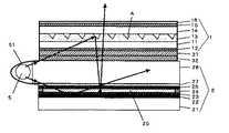
本発明による光学フィルムは、透明フィルムの片面に粘着層を有し、他面にフィルム面に対する傾斜角が35〜48度で略一定方向を向く光路変換斜面と前記光路変換斜面間に設けられた平坦面とを具備する溝構造の複数を有すると共に、その溝構造形成面が、前記平坦面に沿って貼付された平坦かつ透明なカバーフィルムで被覆されてなり、かつそのカバーフィルムの前記溝構造形成面と反対側に少なくとも反射防止層と防汚層を有するものからなる。その例を図1(a)〜(c)に示した。1が光学フィルムで、11が透明フィルム、12が粘着層、13が光路変換斜面A1を具備する溝構造Aの複数を有する層すなわち光路変換手段Aの繰り返し構造層、14がカバーフィルム、15が反射防止層、16が防汚層であり、17は剥離シート、18は防眩層である。なお光路変換手段Aの繰り返し構造は、透明フィルム11と同体に形成されていてもよい。
【0011】
光学フィルム1は、図2に例示した如く側面に照明装置5を有する液晶表示パネル2の視認面に沿う方向に配置し、前記照明装置による側面方向からの入射光ないしその伝送光を矢印の如く光路変換斜面A1を介し反射させ透明フィルム11の当該斜面を有しない面側に、従って液晶表示パネルの視認方向に光路変換して透明フィルムより出射させ、その出射光を液晶表示パネル等の照明光(表示光)として利用できるようにすることを目的とする。
【0012】
透明フィルム11は、照明装置等を介して入射させる光の波長域に応じそれに透明性を示す適宜な材料にて形成しうる。ちなみに可視光域では例えばアクリル系樹脂やポリカーボネート系樹脂、セルロース系樹脂やノルボルネン系樹脂、ポリエステル系樹脂やポリエーテルスルホン系樹脂、ポリアミド系樹脂やポリイミド系樹脂、ポリオレフィン系樹脂やポリエーテル系樹脂、ポリ塩化ビニルやスチレン系樹脂等で代表される透明樹脂、あるいはアクリル系やウレタン系、アクリルウレタン系やエポキシ系、シリコーン系等の熱や紫外線、電子線等の放射線で重合処理しうる硬化型樹脂などがあげられる。就中、複屈折を示さないか複屈折の小さい材料を用いることが好ましい。また接着処理にて透明フィルムに内部応力が発生する場合があり、かかる内部応力による位相差の発生を防止する点よりは光弾性係数の小さい材料を用いることが好ましい。
【0013】
輝度ムラや色ムラを抑制して表示ムラの少ない液晶表示装置を形成する点より好ましく用いうる透明フィルムは、前記の如く面内の平均位相差が小さいもの、就中30nm以下のものである。すなわち図2に例示した如く小さい位相差の透明フィルム11とすることにより偏光板31等を介した直線偏光が入射した場合にその偏光状態を良好に維持できて表示品位の低下防止に有利である。ちなみに通例のポリエステルフィルム等では約2000nmの位相差を示すが、位相差の大きいフィルムでは偏光板等を介した直線偏光が入射した場合に位相差の影響で入射角や反射角によっては色変化で虹色化したり、偏光状態が変化して伝送効率や出射効率が低下したりして輝度ムラや色ムラ等の表示ムラを生じやすくなる。表示ムラ防止の点より透明フィルムにおける面内の好ましい平均位相差は、20nm以下、就中15nm以下、特に10nm以下であり、その位相差の場所毎のバラツキが可及的に小さいものがより好ましい。
【0014】
また伝送光の透明フィルムへの入射角が45度を超えやすいことを考慮すると透明フィルムの厚さ方向の平均位相差も前記した面内の平均位相差と同様に影響しやすく、表示ムラ防止等の点よりその厚さ方向の平均位相差は50nm以下、就中30nm以下、特に20nm以下であることが好ましい。かかる低位相差の透明フィルムの形成は、例えば既成のフィルムを焼鈍処理する方式等にて内部の光学歪みを除去する方式などの適宜な方式にて行いうる。
【0015】
透明フィルムの好ましい形成方式は、キャスティング方式にて位相差の小さいものを形成する方式である。なお透明フィルムにおける前記の位相差条件は、光学フィルムの表示に利用する範囲で満足されればよく、光学フィルムの全面で満足される必要はない。また当該位相差は、可視域の光、特に波長550nmの光に基づくものであることが好ましい。透明フィルム11は、位相差制御等を目的に同種又は異種の樹脂からなる2層以上の重畳体として形成されていてもよく、図例の如く1種の材料による一体的単層物として形成されている必要はない。透明フィルムの厚さは、適宜に決定しうるが一般には薄型化などの点より300μm以下、就中5〜200μm、特に10〜100μmとされる。
【0016】
透明フィルム11は、前記した目的を達成する点より図1に例示した如く側面方向からの入射光ないしその伝送光を所定方向に反射して光路変換する斜面A1をフィルムの片面に有するものとされる。その場合、本発明にては光路変換を介して正面方向への指向性に優れる照明光を得る点より図1に示した如く、フィルム面A4に対する傾斜角θが35〜48度で、略一定方向を向く光路変換斜面A1を具備する溝構造(凹部)からなる光路変換手段Aの繰り返し構造を有するものとされる。
【0017】
前記した光路変換手段Aの例を図1(a)〜(c)に示した。その(a)、(b)では光路変換手段Aが断面略三角形のものからなり、(c)では断面略四角形のものからなる。また(a)では二等辺三角形による2面の光路変換斜面A1を有し、(b)では光路変換斜面A1と傾斜角が斜面A1よりも大きい急斜面A2を有する光路変換手段Aからなる。一方、(c)では2面の光路変換斜面A1と平坦面A3を有する光路変換手段Aからなる。
【0018】
前記した例のように光路変換手段は、等辺面ないし同じ傾斜角の斜面からなる凹部にても形成できるし、光路変換斜面と急斜面又は緩斜面ないし傾斜角が相違する斜面からなる凹部にても形成でき、その斜面形態は光を入射させる側面方向の数や位置にて適宜に決定することができる。従って短辺の光路変換斜面A1と長辺の緩斜面、就中フィルム面に対する傾斜角が10度以下の斜面を単位とする光路変換手段Aが隣接連続状態の繰返し構造として形成されたものであってもよい。
【0019】
上記した正面方向への指向性等の特性を達成する点などより好ましい光学フィルムは、光路変換斜面A1が向く略一定方向を光が入射する側面方向と対面する方向としたものである。従って光学フィルムの2側面以上の側面方向から光を入射させる場合には、その数と位置に対応して光路変換斜面A1を有する光学フィルムとしたものが好ましく用いられる。
【0020】
ちなみに光学フィルムの対向する2側面を光が入射する側面方向とする場合には、図1(a)の如き断面略二等辺三角形からなる光路変換手段Aによる2面の光路変換斜面A1や、図1(c)の如き断面略台形ないし四角形からなる光路変換手段Aによる2面の光路変換斜面A1をその稜線が前記側面方向に沿う方向となる状態で有するものの如く、略一定方向を向く光路変換斜面がその一面を基準にそれとは反対方向を向く面を含む状態で2面以上有する光学フィルム1が好ましく用いられる。なお光路変換斜面A1は、その稜線が光学フィルムの縦横の隣接2側面に沿う方向や、さらには対向及び縦横を含む3側面以上に沿う方向に形成されていてもよい。
【0021】
上記したように光路変換斜面A1は、側面方向よりの入射光ないしその伝送光の内、その面A1に入射する光を反射して光路変換する役割をする。その場合、図1(a)に例示の如く光路変換斜面A1のフィルム面に対する傾斜角θを35〜48度とすることにより側面方向よりの入射光ないしその伝送光をフィルム面に対し垂直性よく光路変換して正面への指向性に優れる照明光を効率よく得ることができる。
【0022】
前記の傾斜角θが35度未満では反射光の光路が正面方向より30度以上の方向に大きくずれて表示に有効利用しにくく正面方向の輝度に乏しくなり、48度を超えると側面方向よりの入射光ないしその伝送光を全反射させる条件から外れて光路変換斜面よりの漏れ光が多くなり側面方向よりの入射光の光利用効率に乏しくなる。正面への指向性に優れる光路変換や漏れ光の抑制等の点より光路変換斜面A1の好ましい傾斜角θは、伝送光のスネルの法則による屈折に基づく全反射条件などを考慮して38〜45度、就中40〜44度である。
【0023】
上記の光路変換斜面A1を具備する光路変換手段Aは、光学フィルムの薄型化を目的に繰返し構造として形成される。その場合、側面方向からの入射光を後方に反射し対向側面側に効率よく伝送して光学フィルム全面で可及的に均一に発光させる点よりは、フィルム面に対する傾斜角が5度以下、就中4度以下、特に3度以下の緩斜面ないし図1に例示の如く当該傾斜角が略0度の面A3やフィルム面A4からなる平坦面を含む構造とする。従って図1(b)に例示の急斜面A2を含む光路変換手段Aでは、その急斜面の角度を35度以上、就中50度以上、特に60度以上としてフィルム面A4の幅を広くできる構造とすることが好ましい。
【0024】
また前記の平坦面は、図2の例の如く光学フィルム1を反射型の液晶表示パネル2のフロントに配置した場合や、光学フィルムの背面側に反射層を設けてバックに配置した場合に、点灯モードによる表示光の透過部分や、外光の入射部分及びその入射光の反射層22を介した反射光の透過部分として機能させることができ、これにより照明装置による点灯モードや外光による外光モードでの表示を可能として点灯・外光両用型の液晶表示装置の形成を可能とする。
【0025】
前記において明るい表示を得る点よりは、フィルム面に対する傾斜角が5度以下の緩斜面や平坦面A3、A4の占有面積ないし幅を光路変換手段Aを形成したフィルム片面に基づいて当該傾斜角が35度以上の斜面A1やA2によるそれの5倍以上、就中8倍以上、特に10倍以上とすることが好ましい。これは前記した外光の入射効率や反射層を介した反射光の透過効率の向上を目的とする。
【0026】
光路変換手段Aは、その稜線が光が入射する側面方向に平行又は傾斜状態で沿うように設けられるがその場合、光路変換手段Aは透明フィルムの一端から他端にわたり連続して形成されていてもよいし、断続的に不連続に形成されていてもよい。不連続に形成する場合、伝送光の入射効率や光路変換効率などの点よりその溝構造の側面方向に沿う方向の長さを深さの5倍以上とすることが好ましく、また光学フィルム上での均一発光化の点より前記長さを500μm以下、就中10〜480μm、特に50〜450μmとすることが好ましい。
【0027】
光路変換手段Aを形成する斜面は、直線面や屈折面や湾曲面等の適宜な面形態に形成されていてよく、光路変換手段Aの断面形状やそれを介した光路変換斜面A1の繰返しピッチについては特に限定はない。光路変換斜面A1が点灯モードでの輝度決定要因となることより光学フィルム上での発光の均一性や、点灯・外光両用型では外光モードでの発光の均一性などに応じて適宜に決定でき、その分布密度にて光路変換光量を制御することができる。
【0028】
従って斜面A1、2の傾斜角等がシートの全面で一定な形状であってもよいし、吸収ロスや先の光路変換による伝送光の減衰に対処して光学フィルム上での発光の均一化を図ることを目的に、光が入射する側の側面から遠離るほど光路変換手段Aを大きくしてもよい。また一定ピッチの光路変換手段Aとすることもできる。
【0029】
さらに光が入射する側の側面から遠離るほど徐々にピッチを狭くして光路変換手段Aの分布密度を多くしたものとすることもできし、ランダムピッチにて光学フィルム上での発光の均一化を図ることもできる。ランダムピッチは、画素との干渉によるモアレの防止の点よりも有利である。よって光路変換手段Aは、ピッチに加えて形状等も異なる溝構造の組合せからなっていてもよい。
【0030】
光路変換斜面A1が液晶表示パネルの画素とオーバーラップすると表示光の透過不足で不自然な表示となることがあり、それを防止する点などよりはそのオーバーラップ面積を可及的に小さくして平坦面A3、4を介した充分な光透過率を確保することが好ましい。かかる点より液晶表示パネルの画素ピッチが一般に100〜300μmであることも考慮して光路変換斜面A1は、そのフィルム面に対する投影幅に基づいて40μm以下、就中3〜20μm、特に5〜15μmとなるように形成することが好ましい。かかる投影幅は、一般に蛍光管のコヒーレント長が20μm程度とされている点などより回折による表示品位の低下を防止する点よりも好ましい。
【0031】
一方、前記の点よりは光路変換斜面A1の間隔の大きいことが好ましいが、他方で光路変換斜面は上記したように側面方向よりの入射光の光路変換による実質的な照明光形成の機能部分であるから、その間隔が広すぎると点灯時の照明が疎となって不自然な表示となる場合がありそれらを鑑みた場合、光路変換斜面A1の繰返しピッチは、5mm以下、就中20μm〜3mm、特に50μm〜2mmとすることが好ましい。
【0032】
また光路変換手段の繰返し構造と液晶表示パネルの画素が干渉してモアレを生じる場合がある。モアレの防止は、その繰返し構造のピッチ調節で行いうるが、上記したように繰返し構造のピッチには好ましい範囲がある。従ってそのピッチ範囲でモアレが生じる場合の解決策が問題となる。本発明においては、画素に対して溝構造を交差状態で配列しうるように溝構造の稜線を側面方向に対し傾斜する状態に形成してモアレを防止する方式が好ましい。
【0033】
前記の場合、側面方向に対する傾斜角が大きすぎると光路変換斜面A1を介した反射に偏向を生じて光路変換の方向に大きな偏りが発生し表示品位の低下原因となりやすいことから、その稜線の側面方向に対する傾斜角は、±30度以内、就中±25度以内、±20度以内とすることが好ましい。なお±の符号は側面方向を基準とした稜線の傾斜方向を意味する。液晶表示パネルの解像度が低くてモアレを生じない場合やモアレを無視しうる場合には、かかる稜線は側面方向に平行なほど好ましい。
【0034】
光路変換手段を有する透明フィルムは、例えば熱可塑性樹脂を所定の形状を形成しうる金型に加熱下に押付て形状を転写する方法、加熱溶融させた熱可塑性樹脂あるいは熱や溶媒を介して流動化させた樹脂を所定の形状に成形しうる金型に充填する方法、熱や紫外線、あるいは電子線等の放射線で重合処理しうる液状樹脂を所定の形状を形成しうる型に充填ないし流延して重合処理する方法などの適宜な方法で形成することができる。
【0035】
光路変換手段を有する透明フィルムの好ましい形成方法は例えば、透明フィルムの片面に紫外線ないし放射線等で重合処理しうる硬化型樹脂を塗工し、その塗工層を金型の所定溝構造の形成面に密着させて紫外線や放射線等の照射により硬化処理した後、金型よりその透明フィルムを剥離回収する方法の如く、所定の溝構造を有する金型を介して透明フィルムの片面に光路変換斜面を具備する溝構造の繰り返し構造を付加する方法である。
【0036】
前記の如く光路変換手段を有する透明フィルムは、光路変換手段を有する状態に一体成形して得ることもできるし、図例の如く透明フィルム11の片面に光路変換手段の形成層13を付加する方法にても得ることができる。後者の場合、付加する光路変換手段の形成層13と透明フィルム11の屈折率差が大きいと界面反射等にて出射効率が大きく低下する場合があり、それを防止する点より透明フィルムと光路変換手段の形成層との屈折率差を可及的に小さくすることが好ましい。
【0037】
前記の特に好ましい屈折率差は、0.10以内、就中0.05以内である。またその場合、透明フィルムよりも付加する光路変換手段の形成層の屈折率を高くすることが出射効率の点より好ましい。なお光路変換手段の形成層は、上記の透明フィルムに準じ、照明装置等を介して入射させる光の波長域に応じそれに透明性を示す適宜な材料にて形成することができる。
【0038】
光学フィルムは、図1の例の如く透明フィルム11の溝構造Aを有しない面に粘着層12を設けたものとされる。かかる粘着層は、液晶表示パネル等の支持部材に光学フィルムを接着するためのものであり粘着層を介した接着処理は、光路変換手段Aの光路変換斜面A1を介した反射効率、ひいては側面方向よりの入射光の有効利用による輝度向上などを目的とする。
【0039】
粘着層の形成には、ゴム系やアクリル系、ビニルアルキルエーテル系やシリコーン系、ポリエステル系やポリウレタン系、ポリエーテル系やポリアミド系、スチレン系などの適宜なポリマーをベースポリマーとする粘着剤などを用いうる。就中アクリル酸ないしメタクリル酸のアルキルエステルを主体とするポリマーをベースポリマーとするアクリル系粘着剤の如く透明性や耐候性や耐熱性などに優れるものが好ましく用いられる。
【0040】
前記において本発明では屈折率差による界面反射で光が光学フィルム内に閉じ込められて出射できなくなることを防止し、出射できずに損失となる光量を抑制する点より、透明フィルムとの屈折率差が0.12以内、就中0.10以内、特に0.05以内の粘着層が好ましく用いられる。また粘着層は、それに例えばシリカやアルミナ、チタニアやジルコニア、酸化錫や酸化インジウム、酸化カドミウムや酸化アンチモン等の導電性のこともある無機系粒子や、架橋又は未架橋ポリマー等の有機系粒子などの適宜な透明粒子を1種又は2種以上含有させて光拡散型のものとすることもできる。
【0041】
なお粘着層に対してはそれを実用に供するまでの間、異物の混入等の防止を目的に図1の例の如く剥離シート17を仮着してカバーしておくことが好ましい。さらに前記と同様の理由で粘着層を接着する前記液晶表示パネル等の支持部材との屈折率差も0.15以内、就中0.10以内、特に0.05以内であることが好ましい。
【0042】
光学フィルムは、光路変換斜面の保護、特に汚染防止を目的に図例の如く透明フィルム11の溝構造形成面13を透明なカバーフィルム14にて被覆したものとされる。溝構造に汚れが詰まると上記した光路変換機能が低下し、汚染を払拭する際にも溝内に汚れが詰まりやすい。カバーフィルムは、照明装置等を介して入射させる光の波長域に応じそれに透明性を示す適宜な材料にて形成することができ、上記した透明フィルムに準じうる。
【0043】
図例の如くカバーフィルム14の外側には反射防止層15と防汚層16が少なくとも設けられる。反射防止層は、視認を阻害する外光の表面反射の抑制を目的とし、例えば蒸着方式による誘電体の多層膜の如き干渉性の蒸着膜を形成する方式、ディッピング方式やスプレー方式等を含む適宜な塗工方式にて低屈折率膜を形成する方式などの適宜な方式にて形成することができる。
【0044】
一方、防汚層は、指紋等の汚染を付着しにくくし、また付着汚染を払拭除去しやすくして反射防止層等の機能保護などを目的とし従って通例、図例の如く最表面に設けられる。防汚層についても例えばフッ素含有樹脂等の表面エネルギーの小さい材料による塗工膜などとして適宜に形成することができる。
【0045】
前記において溝構造に反射防止層を直接設けても汚染問題は解消しないし、反射防止層や防汚層を塗工方式にて溝構造に直接形成すると凹部に溜まりを生じて溝形状が変化し上記した光路変換機能が阻害されやすいが、本発明ではカバーフィルムにて溝構造が防御されてかかる問題の誘発を防止することができる。
【0046】
カバーフィルムの外側には更に図1(c)に例示の如く必要に応じて防眩層(ノングレア層)18などの適宜な層を設けることもできる。防眩層は、外光を散乱反射させて外光の映込みによる視認阻害の防止等を目的とし、反射防止層と組合せることで視認性を効果的に向上させることができる。防眩層も例えばサンドブラスト方式やエンボス加工方式等の粗面化方式、シリカ等の透明粒子の配合方式などの種々の方式で表面を微細凹凸構造化した樹脂層などとして適宜に形成することができる。
【0047】
前記した反射防止層や防汚層、防眩層等は、溝構造の形成面に接着したカバーフィルムに対して後付加方式で設けることもできるし、予めカバーフィルムに設けてそのフィルムを溝構造の形成面に接着して設けることもできる。なお図1(c)の如く防眩層18を設ける場合、その位置は反射防止層15の内側とすることが視認性の向上等の点より有利である。その場合、防眩層をウレタンアクリル系紫外線硬化型樹脂の如きカバーフィルムよりも硬質の樹脂で形成することによりハードコート性を付加することができ、また反射防止層の密着力を向上させることができる。さらに高屈折率、就中、屈折率が1.55以上の樹脂による防眩層とすることにより反射防止層の効果を向上させることができる。
【0048】
本発明による光学フィルムは、照明装置等による側面方向からの入射光ないしその伝送光を光路変換斜面を介し視認に有利な垂直性に優れる方向に光路変換して光利用効率よく出射し、また外光に対しても良好な透過性を示し、図2に例示した如く1又は2以上の側面に照明装置5を配置した液晶表示パネル2の視認背面側(バック)や視認側(フロント)に配置して明るくて見やすい透過型や低消費電力性に優れる点灯・外光両用型の液晶表示装置などの種々の装置を形成することができる。
【0049】
ちなみに図2の例ではフロント式の液晶表示装置を示しており、これによれば照明装置を介した側面方向よりの入射光の殆どが液晶表示パネルにおける各層の厚さ比に基づいてその上下のセル基板21、28を介し屈折の法則による反射を介して後方に伝送され、視認側に配置した光学フィルム1の光路変換斜面A1に入射した光が効率よく視認背面方向に光路変換され、他の光は全反射にて後方に伝送されて後方における光路変換斜面A1に入射し効率よく視認背面方向に光路変換されて液晶セル内に設けた反射層22で反射され、その反射による反転光が光学フィルムの平坦面A4より出射して明るさに優れる表示を達成することができる。
【0050】
前記において液晶表示パネル2としては、少なくとも液晶セルを有する適宜な透過型や反射型のもの、すなわち図例の如くセル基板21、28の間にシール材24を介し液晶25を封入してなる液晶セルを少なくとも有して、光学フィルム1を配置した側からの入射光を液晶等による制御を介し表示光として他方側あるいは反射層を介した反転により入射側から出射するものを用いることができ、その種類について特に限定はない。
【0051】
ちなみに前記した液晶セルの具体例としては、TN液晶セルやSTN液晶セル、IPS液晶セルやHAN液晶セル、OCB液晶セルやVA液晶セルの如きツイスト系や非ツイスト系、ゲストホスト系や強誘電性液晶系の液晶セル、あるいは光拡散型の液晶セルなどがあげられ、液晶の駆動方式も例えばアクティブマトリクス方式やパッシブマトリクス方式などの適宜なものであってよい。その液晶の駆動は通例、図2に例示の如く一対のセル基板21、28の内側に設けた透明電極27あるいは反射型の電極22を介して行われる。
【0052】
セル基板については、ガラスや樹脂などから適宜な基板を用いることができ、就中、表示品位等の点より視認側の基板は光学的に等方性の材料からなるものが好ましい。また輝度や表示品位の向上等の点より青ガラス板に対する無アルカリガラス板の如く視認側の基板は無色透明性に優れるものが好ましく、さらに軽量性等の点よりは樹脂基板が好ましい。セル基板の厚さについては、特に限定はなく液晶の封入強度などに応じて適宜に決定しうる。一般には光伝送効率と薄型軽量性のバランスなどの点より10μm〜5mm、就中50μm〜2mm、特に100μm〜1mmの厚さとされる。
【0053】
液晶セルの形成に際しては必要に応じ、液晶を配向させるためのラビング処理膜等からなる配向膜やカラー表示のためのカラーフィルタなどの適宜な機能層の1層又は2層以上を設けることができる。なお図例の如く、配向膜23、26は通常、電極22、27の上に形成され、また図外のカラーフィルタは通常、セル基板21、28の一方における基板と電極の間に設けられる。
【0054】
さらに反射型の液晶表示装置を形成する場合には反射層が設けられるが、その配置位置は図2の如く電極22等による液晶セル内であってもよいし、視認背面側のセル基板21の外側であってもよい。その反射層は、従来に準じた白色シートなどの適宜なものにて形成することができる。就中、例えばアルミニウムや銀、金や銅やクロム等の高反射率の金属ないしその合金の粉末をバインダ樹脂中に含有させた塗工層、前記の金属等や誘電体多層膜を真空蒸着方式やスパッタリング方式等の適宜な薄膜形成方式で付設してなる層、前記の塗工層や付設層をフィルム等からなる基材で支持した反射シート、金属箔などからなる高反射率の反射層が好ましい。
【0055】
液晶表示パネルは、図2の例の如く液晶セルに偏光板31や位相差板32、光拡散層等の適宜な光学層の1層又は2層以上を付加したものであってもよい。偏光板は直線偏光を利用した表示の達成を目的とし、位相差板は液晶の複屈折性による位相差の補償等による表示品位の向上などを目的とする。また光拡散層は、表示光の拡散による表示範囲の拡大や光学フィルムの斜面を介した輝線状発光の平準化による輝度の均一化、液晶表示パネル内の伝送光の拡散による光学フィルムへの入射光量の増大などを目的とする。
【0056】
前記の偏光板としては、適宜なものを用いることができ特に限定はない。高度な直線偏光の入射による良好なコントラスト比の表示を得る点などよりは、例えばポリビニルアルコール系フィルムや部分ホルマール化ポリビニルアルコール系フィルム、エチレン・酢酸ビニル共重合体系部分ケン化フィルムの如き親水性高分子フィルムにヨウ素や二色性染料等の二色性物質を吸着させて延伸したものからなる吸収型偏光フィルムやその片側又は両側に透明保護層を設けたものなどの如く偏光度の高いものが好ましく用いうる。
【0057】
前記透明保護層の形成には、透明性や機械的強度、熱安定性や水分遮蔽性などに優れるものが好ましく用いられ、その例としては上記の透明フィルムで例示したものなどがあげられる。透明保護層は、フィルムとしたものの接着方式やポリマー液等の塗布方式などにより付与することができる。なお偏光板は、図例の如く液晶セルの片側にのみ設けることもできるし、液晶セルの両側に設けることもできる。
【0058】
一方、位相差板としても例えば上記の透明フィルムで例示したものなどの適宜なポリマーからなるフィルムを一軸や二軸等の適宜な方式で延伸処理してなる複屈折性フィルム、ネマチック系やディスコティック系等の適宜な液晶ポリマーの配向フィルムやその配向層を透明基材で支持したものなどの適宜なものを用いることができ、熱収縮性フィルムの加熱収縮力の作用下に厚さ方向の屈折率を制御したものなどであってもよい。図例の如く補償用の位相差板32は通例、視認側又は/及び背面側の偏光板31と液晶セルの間に必要に応じて配置され、その位相差板には波長域などに応じて適宜なものを用いうる。また位相差板は、位相差等の光学特性の制御を目的に2層以上を重畳して用いることもできる。
【0059】
また光拡散層についても上記の防眩層に準じた表面微細溝構造を有する塗工層や拡散シートなどによる適宜な方式にて設けることができる。光拡散層は、上記した透明粒子配合の粘着層12に準じて偏光板31と位相差板32の接着を兼ねる粘着層として配置することもでき、これにより薄型化を図かることができる。光拡散層は、偏光板よりも外側(視認側)に配置することもできるが、偏光板よりも液晶セル側に配置することで外光が偏光板で吸収された後に光拡散層に入射することとなり、光拡散層を介した後方散乱による反射損を抑制できて有利である。
【0060】
一方、液晶表示パネルの側面に配置する照明装置は、液晶表示装置の照明光として利用する光を液晶表示パネルの側面から入射させることを目的とする。これによりパネルのバックやフロントに配置する光学フィルムとの組合せにて液晶表示装置の薄型軽量化を図ることができる。照明装置としては適宜なものを用いることができ、例えば(冷,熱)陰極管等の線状光源、発光ダイオード等の点光源やそれを線状や面状等に配列したアレイ体、あるいは点光源と線状導光板を組合せて点光源からの入射光を線状導光板を介し線状光源に変換するようにした照明装置などが好ましく用いうる。
【0061】
照明装置は、液晶表示パネル2における1又は2以上の側面に配置することができる。照明装置を2以上の側面に配置する場合、その複数の側面は対向する側面の組合せであってもよいし、縦横に交差する側面の組合せであってもよく、それらを併用した3側面以上の組合せであってもよい。照明装置は、その点灯による点灯モードでの視認を可能とするものであり、点灯・外光両用型の液晶表示装置の場合に外光による外光モードにて視認するときには点灯の必要がないので、その点灯・消灯を切り替えうるものとされる。その切り替え方式には任意な方式を採ることができ、従来方式のいずれも採ることができる。なお照明装置は、発光色を切り替えうる異色発光式のものであってもよく、また異種の照明装置を介して異色発光させうるものとすることもできる。
【0062】
図例の如く照明装置5に対しては、必要に応じ発散光を液晶表示パネル2の側面に導くためにそれを包囲するリフレクタ51などの適宜な補助手段を配置した組合せ体とすることもできる。リフレクタとしては、高反射率の金属薄膜を付設した樹脂シートや白色シートや金属箔などの適宜な反射シートを用いうる。リフレクタは、その端部を液晶表示パネルのセル基板等の端部に接着する方式などにて照明装置の包囲を兼ねる固定手段として利用することもできる。
【0063】
なお本発明において上記した液晶表示装置を形成する液晶セルや偏光板や位相差板等の光学素子ないし部品は、全体的又は部分的に積層一体化されて固着されていてもよいし、分離容易な状態に配置されていてもよい。界面反射の抑制によるコントラストの低下防止などの点よりは固着状態にあることが好ましい。その固着密着処理には、粘着剤等の適宜な透明接着剤を用いることができ、その透明接着層に上記した透明粒子等を含有させて拡散機能を示す接着層などとすることもできる。また前記の光学素子ないし部品、特に視認側のそれには例えばサリチル酸エステル系化合物やベンゾフェノン系化合物、ベンゾトリアゾール系化合物やシアノアクリレート系化合物、ニッケル錯塩系化合物等の紫外線吸収剤で処理する方式などにより紫外線吸収能をもたせることもできる。
【0064】
【実施例】
実施例1
予め所定形状に加工した金型にアクリル系の紫外線硬化型樹脂(東亞合成社製、アロニックスUV−3701)をスポイトにて滴下充填し、その上に厚さ80μmのトリアセチルセルロース(TAC)フィルム(表面ケン化処理物)を静置しゴムローラで密着させて余分な樹脂と気泡を除去しメタルハライドランプにて紫外線を照射して硬化処理した後、金型から剥離し所定寸法に裁断して屈折率1.49のTACフィルムの片面に屈折率1.533の光路変換手段の繰り返し層を有する透明フィルムを得た。
【0065】
次に厚さ40μmのTACフィルムの片面に真空蒸着方式により二酸化珪素と二酸化チタンからなる反射防止層を形成し、その上にフルオロアルキルシランからなる防汚層を塗工形成してなるカバーフィルムをその反射防止層等が外側となるように前記で得た透明フィルムの溝構造からなる光路変換手段の形成面に接着剤を介して接着し、その透明フィルムの光路変換手段を有しない面に屈折率1.47の粘着層を付設して光学フィルムを得た。この光学フィルムは、幅が60mm、奥行が45mmであり、稜線が幅方向に平行な連続溝を210μmのピッチで有し、その光路変換斜面A1の傾斜角が42.5〜43度で幅が8〜13μmであり、急斜面A2の傾斜角が67〜67.5度で平坦部(A4)の面積が光路変換斜面と急斜面のフィルム面に対する投影合計面積の9.8倍以上の光路変換手段(図1b)を有する。
【0066】
次に市販のTN型液晶セルの表裏に偏光板を貼着し、その視認背面側の偏光板の外側に粗面拡散型の銀反射板を貼着してなるノーマリーホワイトの反射型TN液晶表示パネルの側面に冷陰極管を配置して銀蒸着の反射シートからなるリフレクタにて包囲し、その両端部をパネルの上下面に接着して冷陰極管を固定した後その視認側の偏光板に前記の光学フィルムをその粘着層を介し光路変換斜面が冷陰極管と平行に対面するように接着して点灯・外光両用型の液晶表示装置を得た。
【0067】
実施例2
サンドブラスト加工にて粗面化した金型にアクリル系の紫外線硬化型樹脂をスポイトにて滴下充填し、その上にケン化処理したカバーフィルムを静置しゴムローラで密着させて余分な樹脂と気泡を除去しメタルハライドランプにて紫外線を照射して硬化処理した後、金型から剥離し所定寸法に裁断して防眩処理面を有するカバーフィルムを得、その上に反射防止層と防汚層を設けてそれを用いたほかは実施例1に準じて光学フィルムを得、それを用いて点灯・外光両用型の液晶表示装置を得た。
【0068】
比較例1
透明フィルムの光変換手段形成面に直接反射防止層を形成し、それを光学フィルムとして用いたほかは実施例1に準じて点灯・外光両用型の液晶表示装置を得た。
【0069】
比較例2
透明フィルムの光変換手段形成面に直接反射防止層を形成し、その上に防汚層を塗工形成してそれを光学フィルムとして用いたほかは実施例1に準じて点灯・外光両用型の液晶表示装置を得た。
【0070】
比較例3
実施例1に準じて光路変換斜面の傾斜角が約30度で幅が7〜11μmであり、急斜面A2の傾斜角が約70度でピッチが210μm、平坦部の面積が光路変換斜面と急斜面のフィルム面に対する投影合計面積の8.1倍以上の光路変換手段を有する光学フィルムを得、それを用いて点灯・外光両用型の液晶表示装置を得た。
【0071】
比較例4
実施例1に準じて光路変換斜面の傾斜角が約50度で幅が10〜16μmであり、急斜面A2の傾斜角が約70度でピッチが210μm、平坦部の面積が光路変換斜面と急斜面のフィルム面に対する投影合計面積の9.9倍以上の光路変換手段を有する光学フィルムを得、それを用いて点灯・外光両用型の液晶表示装置を得た。
【0072】
比較例5
反射防止層と防汚層を有しないカバーフィルムを用いたほかは実施例1に準じて光学フィルムを得、それを用いて点灯・外光両用型の液晶表示装置を得た。
【0073】
比較例6
防汚層のみを有しないカバーフィルムを用いたほかは実施例1に準じて光学フィルムを得、それを用いて点灯・外光両用型の液晶表示装置を得た。
【0074】
評価試験
実施例、比較例で得た点灯・外光両用型の液晶表示装置について暗室中、液晶表示パネルに電圧を印加しない状態で冷陰極管を点灯させた点灯モードによる装置中央部での正面輝度を輝度計(トプコン社製、BM7)にて調べた。
【0075】
前記の結果を次表に示した。
表より、実施例1、2、比較例1、5,6では比較例2〜4に比べて点灯モードによる優れた正面輝度の達成されていることがわかる。比較例2〜4では大きい角度で出射する光量が多くて正面方向の輝度に乏しく、特に比較例3、4では光源とは反対の方向に光が大角度で出射されて表示に寄与しにくい出射光であった。比較例2では防汚層が溝構造に入りその形状を変化させたためであり、比較例3、4では光変換斜面の傾斜角が不適当であるためである。また点灯モードにおいて液晶表示パネルに電圧を印加した状態での視認では比較例3を除いて問題はなく良好な表示品位であったが、比較例3では見にくかった。
【0077】
一方、冷陰極管を消灯したリング状照明による外光を15度の角度で入射させる外光モードにおける液晶表示パネルへの電圧印加状態において、実施例1、2及び比較例1、2、4、6では像の乱れ等のない明るい良好な表示であったが、比較例3では像の乱れが大きく、比較例5でもリング状照明の映り込みがあって見にくかった。
【0078】
上記より実施例1、2及び比較例1、6で点灯と外光の両モードにおいて見やすくて明るい表示の達成されていることがわかる。しかし実施例1、2及び比較例1、2、6の液晶表示装置の表面を指紋と粘着剤で汚し、それをヘキサン含浸のウエスで払拭した場合、実施例1、2では容易に払拭できて点灯・外光の両モードでクリアな像に回復して見やすかったが、比較例6では払拭できず、また比較例1、2では粘着剤が溝構造に入り込んで払拭しにくく、その残存で特に点灯モードによる発光効率が著しく低下して見にくかった。残存の粘着剤は、粘着テープによる接着でかなり除去できたがそれには非常に煩雑な作業と多時間を要した。以上より本発明にて導光板による嵩高化、高重量化を回避してフィルム方式による薄型軽量化を達成しつつ、表示品位の良好な液晶表示装置を形成でき、汚染を容易に払拭できることがわかる。
【図面の簡単な説明】
【図1】光学フィルム例(光路変換斜面)の側面説明図
【図2】反射型(点灯・外光両用型)液晶表示装置例の説明断面図
【符号の説明】
1:光学フィルム
11:透明フィルム
12:粘着層
13:光路変換手段の繰り返し構造層
A:光路変換手段
A1:光路変換斜面、A3、4:平坦面
14:カバーフィルム
15:反射防止層
16:防汚層
2:液晶表示パネル
21、28:セル基板
22:反射型電極
25:液晶層
31:偏光板
32:位相差板
5:照明装置[0001]
TECHNICAL FIELD OF THE INVENTION
The present invention relates to an optical film excellent in antifouling property capable of forming a thin, lightweight, bright and easy-to-view liquid crystal display device by efficiently changing the optical path of incident light from the side direction in the viewing direction.
[0002]
BACKGROUND OF THE INVENTION
Reflective liquid crystal display devices are required to be made thinner and lighter for the purpose of reducing the size and weight of portable PCs and mobile phones, etc., but those with a front light with a conventional sidelight type light guide plate require light transmission. It is difficult to reduce the thickness and weight of the light guide plate that is 1 mm thick or more. The same applies to the required thickness of the sidelight-type light guide plate even when a backlight type lighting / external light type liquid crystal display device using a transflective reflector is used.
[0003]
In addition to the above, in the case of a backlight type using a transflective reflector, the addition of the transflective reflector increases the bulk and weight, and the light is dispersed into the transmitted light and reflected light through the transflective reflector. Thus, there is a problem that the visual recognition in the lighting mode is darkened and the visual recognition is darkened even in the outside light mode, and the brightness is difficult to reach that of a reflection-only one with a reflective layer having a high reflectance.
[0004]
[Technical Problem of the Invention]
An object of the present invention is to develop an optical film capable of forming a thin, lightweight, bright and easy-to-view liquid crystal display device by efficiently changing the optical path of incident light from the side direction in the viewing direction.
[0005]
[Means for solving problems]
The present invention provides an optical path conversion slope having an adhesive layer on one side of a transparent film and having an inclination angle of 35 to 48 degrees with respect to the film surface and facing a substantially constant direction.And a flat surface provided between the optical path changing slopes, A plurality of groove structures having a groove structure forming surface,Flat and affixed along the flat surface Covered with a transparent cover film, and the cover filmThe opposite side of the groove structure forming surface The optical film is characterized by comprising at least an antireflection layer and an antifouling layer.
[0006]
【The invention's effect】
According to the optical film of the present invention, it is arranged along the viewing surface of the liquid crystal display panel having the illumination device on the side surface, so that the incident light from the side surface or the transmitted light can be changed to the optical path changing slope of the optical film. Therefore, the optical path can be efficiently changed in the viewing direction of the liquid crystal display panel and used for liquid crystal display, and a liquid crystal display device excellent in thinness and light weight and excellent in display quality can be formed. In addition, by providing a flat surface between the optical path conversion slopes, external light can be made incident efficiently, and the incident light can be reflected through the reflective layer in the same way as the optical path conversion light and used for liquid crystal display. In addition to the mode, an external light mode can be added, and a light-emitting / external light-use liquid crystal display device that is excellent in thinness and light weight and has a good display quality can be formed.
[0007]
The above effect is mainly due to the optical path control type optical film by slope reflection. In other words, the incident light from the side surface or its transmitted light is reflected through the light path changing slope, so that the light path can be changed with good directivity and good visibility in the lighting mode is achieved, and a flat surface is easily formed between the light path changing slopes. It is possible to arrange and transmit external light through the flat surface to ensure sufficient external light incidence, and good visual recognition in the external light mode is also achieved. It is difficult to achieve the above effect by a scattering reflection method through a rough surface such as a scattering sheet. Incidentally, in Japanese Patent Laid-Open No. 5-158033, a reflective liquid crystal is used for display in which illumination light is incident from the side surface of a liquid crystal display panel and totally reflected by a viewing side cell substrate, and the reflected light is scattered by a rough surface type reflector. Teaching a display device.
[0008]
However, in the above case, the light that can be used for display is light that scatters out of the total reflection condition and is emitted from the panel. Generally, the scattered light exhibits a normal distribution having a peak in the regular reflection direction (the 20th liquid crystal display). 3) G510, Tohoku University; Uchida, etc.), the above display light is light that is greatly inclined from the front (vertical) direction and is not effectively used for display, and the display light is dark in the front direction. Even if the diffusivity of the rough reflector is increased, the amount of light that is confined in the panel and cannot be emitted increases, and a dark display is obtained.
[0009]
On the other hand, the optical film of the optical path control type by slope reflection according to the present invention mainly uses light in the regular reflection direction showing a peak, and controls the optical path of the reflected light. In particular, the directivity in the front direction can be easily provided, and a bright display can be achieved even in the reflection mode. In addition, the optical path conversion slope is protected through the cover film, dirt is not easily clogged in the groove, and the contamination can be easily wiped and removed through the antifouling layer, so that the optical path conversion function described above can be maintained for a long time. Can also be used advantageously.
[0010]
DETAILED DESCRIPTION OF THE INVENTION
An optical film according to the present invention has an adhesive layer on one side of a transparent film, and an optical path changing slope having an inclination angle of 35 to 48 degrees with respect to the film surface and facing a substantially constant direction on the other side.And a flat surface provided between the optical path changing slopes, A plurality of groove structures having a groove structure forming surface,Flat and affixed along the flat surface Covered with a transparent cover film, and the cover filmThe opposite side of the groove structure forming surface And at least an antireflection layer and an antifouling layer. Examples thereof are shown in FIGS. 1 is an optical film, 11 is a transparent film, 12 is an adhesive layer, 13 is a layer having a plurality of groove structures A having an optical path changing slope A1, that is, a repeating structure layer of the optical path changing means A, 14 is a cover film, An antireflection layer, 16 is an antifouling layer, 17 is a release sheet, and 18 is an antiglare layer. The repeating structure of the optical path changing unit A may be formed in the same body as the transparent film 11.
[0011]
The
[0012]
The transparent film 11 can be formed of an appropriate material that exhibits transparency according to the wavelength range of light incident through an illumination device or the like. In the visible light region, for example, acrylic resins, polycarbonate resins, cellulose resins, norbornene resins, polyester resins, polyethersulfone resins, polyamide resins, polyimide resins, polyolefin resins, polyether resins, poly Transparent resins typified by vinyl chloride and styrene resins, or curable resins that can be polymerized with radiation such as heat, ultraviolet rays, and electron beams such as acrylic, urethane, acrylic urethane, epoxy, and silicone Is given. In particular, it is preferable to use a material that does not exhibit birefringence or has low birefringence. Moreover, an internal stress may generate | occur | produce in a transparent film by an adhesion | attachment process, and it is preferable to use a material with a small photoelastic coefficient from the point which prevents generation | occurrence | production of the phase difference by this internal stress.
[0013]
A transparent film that can be preferably used from the viewpoint of forming a liquid crystal display device with little display unevenness by suppressing brightness unevenness and color unevenness is one having a small in-plane average retardation, particularly 30 nm or less. That is, by using the transparent film 11 having a small retardation as illustrated in FIG. 2, when linearly polarized light is incident through the polarizing
[0014]
Also, considering that the incident angle of the transmitted light to the transparent film tends to exceed 45 degrees, the average retardation in the thickness direction of the transparent film is likely to be affected in the same manner as the above-mentioned average retardation in the plane, and display unevenness prevention, etc. From this point, the average retardation in the thickness direction is preferably 50 nm or less, more preferably 30 nm or less, and particularly preferably 20 nm or less. The formation of the transparent film having a low retardation can be performed by an appropriate method such as a method of removing internal optical distortion by a method of annealing an existing film.
[0015]
A preferable method of forming the transparent film is a method of forming a film having a small phase difference by a casting method. In addition, the said retardation conditions in a transparent film should just be satisfied in the range utilized for the display of an optical film, and do not need to be satisfied in the whole surface of an optical film. The phase difference is preferably based on light in the visible region, particularly light having a wavelength of 550 nm. The transparent film 11 may be formed as two or more layers of the same kind or different kinds of resin for the purpose of phase difference control or the like, and is formed as an integral single layer by one kind of material as shown in the figure. You don't have to. The thickness of the transparent film can be determined as appropriate, but is generally 300 μm or less, especially 5 to 200 μm, especially 10 to 100 μm, from the viewpoint of thinning.
[0016]
The transparent film 11 has a slope A1 on one side of the film for reflecting the incident light from the side surface or its transmitted light in a predetermined direction to change the optical path as illustrated in FIG. The In that case, in the present invention, as shown in FIG. 1, the inclination angle θ with respect to the film surface A4 is 35 to 48 degrees and substantially constant from the point of obtaining illumination light having excellent directivity in the front direction through optical path conversion. It is assumed that the optical path changing means A has a repeating structure composed of a groove structure (concave portion) having an optical path changing slope A1 that faces the direction.
[0017]
An example of the optical path changing means A described above is shown in FIGS. In (a) and (b), the optical path changing means A has a substantially triangular cross section, and in (c), it has a substantially square cross section. Further, (a) includes two optical path conversion slopes A1 with isosceles triangles, and (b) includes optical path conversion means A having an optical path conversion slope A1 and a steep slope A2 having a larger inclination angle than the slope A1. On the other hand, (c) comprises optical path changing means A having two optical path changing slopes A1 and a flat face A3.
[0018]
As in the example described above, the optical path changing means can be formed in a concave portion made of an equilateral surface or a slope having the same inclination angle, or in a concave portion made of an optical path conversion slope and a steep slope or a gentle slope or a slope having a different inclination angle. It can be formed, and the shape of the slope can be determined as appropriate depending on the number and position of the side surfaces in which light is incident. Therefore, the optical path changing means A having a short side optical path changing slope A1, a long side gentle slope, and an inclined face whose inclination angle with respect to the film surface is 10 degrees or less as a unit is formed as an adjacent continuous state repeating structure. May be.
[0019]
More preferable optical films such as the above-mentioned characteristics such as directivity in the front direction are such that a substantially constant direction facing the light path conversion inclined surface A1 is a direction facing a side direction in which light is incident. Accordingly, when light is incident from two or more side directions of the optical film, an optical film having an optical path conversion slope A1 corresponding to the number and position is preferably used.
[0020]
Incidentally, in the case where the two opposite side surfaces of the optical film are in the direction of the side surface on which light is incident, the two-surface optical path conversion slope A1 by the optical path conversion means A having a substantially isosceles triangle cross section as shown in FIG. Optical path conversion in which the optical path conversion means A having a substantially trapezoidal or quadrangular cross section as shown in 1 (c) has two optical path conversion slopes A1 in a state in which the ridge line is in the direction along the side surface direction. The
[0021]
As described above, the optical path changing slope A1 plays a role of changing the optical path by reflecting the light incident on the face A1 from the incident light from the side surface direction or the transmitted light. In this case, as shown in FIG. 1 (a), the incident light from the side surface direction or its transmitted light is perpendicular to the film surface by setting the inclination angle θ of the optical path changing slope A1 to the film surface to 35 to 48 degrees. It is possible to efficiently obtain illumination light that is converted into an optical path and has excellent directivity toward the front.
[0022]
If the tilt angle θ is less than 35 degrees, the optical path of the reflected light is greatly shifted in the direction of 30 degrees or more from the front direction, making it difficult to effectively use for display, and the brightness in the front direction is poor. When the incident light or the transmitted light is not totally reflected, the leakage light from the optical path changing slope increases, and the light use efficiency of the incident light from the side surface direction becomes poor. The preferable inclination angle θ of the optical path conversion inclined surface A1 is 38 to 45 in consideration of the total reflection condition based on the refraction according to Snell's law of the transmitted light in view of the optical path conversion excellent in directivity to the front and suppression of leakage light. Degree, especially 40-44 degrees.
[0023]
The optical path changing means A having the optical path changing slope A1 is formed as a repeating structure for the purpose of reducing the thickness of the optical film. In that case, the angle of inclination with respect to the film surface is 5 degrees or less from the point that incident light from the side surface direction is reflected backward and efficiently transmitted to the opposite side surface to emit light as uniformly as possible on the entire surface of the optical film. A gentle slope of 4 degrees or less, particularly 3 degrees or less, or a structure including a flat surface composed of a surface A3 or a film surface A4 having an inclination angle of approximately 0 degrees as illustrated in FIG.Do . Accordingly, the optical path changing means A including the steep slope A2 illustrated in FIG. 1B has a structure capable of widening the film surface A4 by setting the angle of the steep slope to 35 degrees or more, especially 50 degrees or more, particularly 60 degrees or more. It is preferable.
[0024]
Further, the flat surface is formed when the
[0025]
Rather than obtaining bright display in the above, the inclination angle with respect to the film surface is 5 degrees or less, and the occupied area or width of the flat surfaces A3 and A4 is determined based on the single side of the film on which the optical path changing means A is formed. It is preferable to set it to 5 times or more, especially 8 times or more, especially 10 times or more of the slope A1 or A2 of 35 degrees or more. This is intended to improve the incident efficiency of external light and the transmission efficiency of reflected light through the reflective layer.
[0026]
The optical path changing means A is provided so that its ridge line is parallel or inclined along the side surface direction on which light is incident. In that case, the optical path changing means A is formed continuously from one end to the other end of the transparent film. Alternatively, it may be formed intermittently discontinuously. When formed discontinuously, the length in the direction along the side surface of the groove structure is preferably at least 5 times the depth from the viewpoint of incident efficiency of transmission light, optical path conversion efficiency, etc. From the viewpoint of uniform light emission, the length is preferably 500 μm or less, more preferably 10 to 480 μm, and particularly preferably 50 to 450 μm.
[0027]
The slope forming the optical path conversion means A may be formed in an appropriate surface form such as a straight surface, a refracting surface, or a curved surface, and the cross-sectional shape of the optical path conversion means A and the repetitive pitch of the optical path conversion slope A1 therethrough There is no particular limitation on. Since the light path conversion slope A1 is a factor for determining the luminance in the lighting mode, it is determined appropriately according to the uniformity of light emission on the optical film and the light emission uniformity in the outside light mode for the lighting / external light type. The optical path conversion light quantity can be controlled by the distribution density.
[0028]
Accordingly, the inclination angle of the slopes A1 and A2 may be a constant shape over the entire surface of the sheet, and the light emission on the optical film is made uniform by coping with absorption loss and attenuation of the transmitted light due to the previous optical path conversion. For the purpose of illustration, the optical path changing means A may be enlarged as the distance from the side surface on which light is incident is increased. Also, the optical path changing means A with a constant pitch can be used.
[0029]
Furthermore, as the distance from the side of the light incident side increases, the pitch can be gradually narrowed to increase the distribution density of the optical path changing means A, and the light emission on the optical film can be made uniform at a random pitch. Can also be planned. The random pitch is more advantageous than prevention of moire due to interference with pixels. Therefore, the optical path changing means A may be composed of a combination of groove structures with different shapes and the like in addition to the pitch.
[0030]
If the light path changing slope A1 overlaps with the pixels of the liquid crystal display panel, the display light may be insufficiently transmitted, resulting in an unnatural display, and the overlap area is made as small as possible to prevent this. It is preferable to ensure a sufficient light transmittance through the flat surfaces A3 and A4. Considering that the pixel pitch of the liquid crystal display panel is generally 100 to 300 μm from this point, the optical path changing slope A1 is 40 μm or less, especially 3 to 20 μm, especially 5 to 15 μm, based on the projection width on the film surface. It is preferable to form it as follows. Such a projection width is more preferable than the point of preventing deterioration of display quality due to diffraction, for example, because the coherent length of the fluorescent tube is generally about 20 μm.
[0031]
On the other hand, it is preferable that the distance between the light path conversion slopes A1 is larger than the above point. On the other hand, the light path conversion slope is a function part of substantial illumination light formation by light path conversion of incident light from the side surface direction as described above. Therefore, if the interval is too wide, lighting at the time of lighting may become sparse and unnatural display may occur. In view of these, the repetitive pitch of the optical path changing slope A1 is 5 mm or less, especially 20 μm to 3 mm. In particular, the thickness is preferably 50 μm to 2 mm.
[0032]
In addition, the repeating structure of the optical path changing means may interfere with the pixels of the liquid crystal display panel to cause moire. Although moiré can be prevented by adjusting the pitch of the repeating structure, there is a preferable range for the pitch of the repeating structure as described above. Therefore, a solution in the case where moire occurs in the pitch range becomes a problem. In the present invention, a method of preventing moire by forming the ridge line of the groove structure to be inclined with respect to the side surface direction so that the groove structure can be arranged in an intersecting state with respect to the pixel.
[0033]
In the above case, if the inclination angle with respect to the side surface direction is too large, the reflection through the optical path conversion inclined surface A1 is deflected, and a large deviation occurs in the optical path conversion direction, which tends to cause deterioration in display quality. The inclination angle with respect to the direction is preferably within ± 30 degrees, in particular within ± 25 degrees, and within ± 20 degrees. The sign “±” means the inclination direction of the ridge line with respect to the side surface direction. When the resolution of the liquid crystal display panel is low and moire is not generated or when moire can be ignored, it is preferable that the ridge line be parallel to the side surface direction.
[0034]
The transparent film having the optical path changing means is, for example, a method of transferring a shape by pressing a thermoplastic resin to a mold capable of forming a predetermined shape under heating, a heat-melted thermoplastic resin, or flowing through heat or a solvent. Filling a mold that can be molded into a predetermined shape, filling a liquid mold that can be polymerized with heat, ultraviolet rays, or radiation such as an electron beam into a mold that can form a predetermined shape Then, it can be formed by an appropriate method such as a polymerization method.
[0035]
A preferable method of forming a transparent film having an optical path changing means is, for example, coating a curable resin that can be polymerized with ultraviolet rays or radiation on one side of the transparent film, and forming the coating layer on a surface on which a predetermined groove structure of the mold is formed. After being cured by irradiation with ultraviolet rays, radiation, etc., an optical path changing slope is formed on one side of the transparent film through a mold having a predetermined groove structure, such as a method of peeling and collecting the transparent film from the mold. This is a method of adding a repeating structure of the groove structure provided.
[0036]
As described above, the transparent film having the optical path changing means can be obtained by integrally forming the optical film with the optical path changing means, or a method of adding the optical path changing
[0037]
The particularly preferred difference in refractive index is within 0.10, especially within 0.05. Moreover, in that case, it is preferable from the point of the emission efficiency that the refractive index of the formation layer of the optical path changing means added is higher than that of the transparent film. The formation layer of the optical path changing means can be formed of an appropriate material exhibiting transparency according to the wavelength range of light incident through an illumination device or the like, in accordance with the transparent film.
[0038]
The optical film has an
[0039]
For the formation of the adhesive layer, use adhesives such as rubber, acrylic, vinyl alkyl ether, silicone, polyester, polyurethane, polyether, polyamide, styrene, etc. Can be used. Among them, those having excellent transparency, weather resistance, heat resistance and the like, such as an acrylic pressure-sensitive adhesive mainly composed of a polymer mainly composed of an alkyl ester of acrylic acid or methacrylic acid, are preferably used.
[0040]
In the above, the present invention prevents the light from being trapped in the optical film due to the interface reflection due to the refractive index difference and cannot be emitted and suppresses the amount of light that cannot be emitted and lost, so that the refractive index difference from the transparent film. Is preferably within 0.12, more preferably within 0.10, and particularly preferably within 0.05. In addition, the adhesive layer includes inorganic particles having conductivity such as silica, alumina, titania, zirconia, tin oxide, indium oxide, cadmium oxide, and antimony oxide, and organic particles such as a crosslinked or uncrosslinked polymer. One kind or two or more kinds of appropriate transparent particles may be contained to obtain a light diffusion type.
[0041]
Note that it is preferable to temporarily cover the adhesive layer with a
[0042]
The optical film is formed by covering the groove
[0043]
As shown in the figure, at least an
[0044]
On the other hand, the antifouling layer is difficult to adhere to fingerprints and the like, and is easy to wipe off and remove the adhering contamination to protect the function of the antireflection layer and so is usually provided on the outermost surface as shown in the figure. . The antifouling layer can also be appropriately formed as a coating film made of a material having a small surface energy such as a fluorine-containing resin.
[0045]
In the above, even if an antireflection layer is directly provided on the groove structure, the contamination problem is not solved, and if the antireflection layer or antifouling layer is formed directly on the groove structure by a coating method, the groove shape changes due to the accumulation in the recess. Although the above-described optical path conversion function is likely to be hindered, in the present invention, the groove structure is protected by the cover film, thereby preventing the problem from being induced.
[0046]
Appropriate layers such as an antiglare layer (non-glare layer) 18 can also be provided on the outside of the cover film as needed as illustrated in FIG. The anti-glare layer is intended to prevent visual disturbance due to reflection of external light by scattering and reflecting external light, and the visibility can be effectively improved by combining with the anti-reflection layer. The antiglare layer can also be suitably formed as a resin layer having a surface with a fine concavo-convex structure by various methods such as a roughening method such as a sandblasting method or an embossing method, or a compounding method of transparent particles such as silica. .
[0047]
The above-mentioned antireflection layer, antifouling layer, antiglare layer, etc. can be provided by a post-addition method with respect to the cover film bonded to the groove structure forming surface, or the film is provided in advance on the cover film. It can also be provided by adhering to the forming surface. In addition, when providing the glare-
[0048]
The optical film according to the present invention changes the optical path of incident light from the side surface by a lighting device or the like or its transmitted light in a direction excellent in verticality that is advantageous for visual recognition through an optical path conversion slope, and emits light efficiently. It also shows good transparency to light and is arranged on the viewing back side (back) and viewing side (front) of the liquid
[0049]
Incidentally, the example of FIG. 2 shows a front-type liquid crystal display device, and according to this, most of incident light from the side surface direction through the illumination device is above and below it based on the thickness ratio of each layer in the liquid crystal display panel. Light transmitted through the
[0050]
In the above, the liquid
[0051]
Incidentally, specific examples of the liquid crystal cell described above include TN liquid crystal cell, STN liquid crystal cell, IPS liquid crystal cell, HAN liquid crystal cell, OCB liquid crystal cell and VA liquid crystal cell, twist type, non-twist type, guest host type and ferroelectricity. Examples of the liquid crystal cell include a liquid crystal cell or a light diffusion type liquid crystal cell, and the liquid crystal driving method may be an appropriate one such as an active matrix method or a passive matrix method. The liquid crystal is usually driven through a
[0052]
As the cell substrate, an appropriate substrate can be used such as glass or resin. In particular, the substrate on the viewing side is preferably made of an optically isotropic material from the viewpoint of display quality. Further, from the viewpoint of improvement in luminance and display quality, the substrate on the viewing side such as an alkali-free glass plate with respect to a blue glass plate is preferably excellent in colorless transparency, and a resin substrate is more preferable in terms of lightness and the like. The thickness of the cell substrate is not particularly limited and can be appropriately determined according to the sealing strength of the liquid crystal. In general, the thickness is 10 μm to 5 mm, especially 50 μm to 2 mm, especially 100 μm to 1 mm, in view of the balance between light transmission efficiency and thin and light weight.
[0053]
When forming the liquid crystal cell, one or two or more appropriate functional layers such as an alignment film composed of a rubbing treatment film for aligning liquid crystals and a color filter for color display can be provided as necessary. . As shown in the drawing, the
[0054]
Further, in the case of forming a reflective liquid crystal display device, a reflective layer is provided, but the position of the reflective layer may be in the liquid crystal cell by the
[0055]
The liquid crystal display panel may be one in which one or two or more appropriate optical layers such as a
[0056]
As the polarizing plate, any suitable one can be used and there is no particular limitation. Higher hydrophilicity such as polyvinyl alcohol film, partially formalized polyvinyl alcohol film, ethylene / vinyl acetate copolymer partially saponified film, etc. A highly polarizing film such as an absorbing polarizing film formed by adsorbing and stretching a dichroic substance such as iodine or a dichroic dye on a molecular film or a transparent protective layer provided on one or both sides thereof. It can be preferably used.
[0057]
For the formation of the transparent protective layer, those excellent in transparency, mechanical strength, thermal stability, moisture shielding properties and the like are preferably used, and examples thereof include those exemplified in the above transparent film. The transparent protective layer can be applied by a bonding method of a film or a coating method of a polymer liquid or the like. The polarizing plate can be provided only on one side of the liquid crystal cell as shown in the figure, or can be provided on both sides of the liquid crystal cell.
[0058]
On the other hand, as a phase difference plate, for example, a birefringent film obtained by stretching a film made of an appropriate polymer such as those exemplified in the above transparent film by an appropriate method such as uniaxial or biaxial, nematic or discotic An appropriate film such as an alignment film of an appropriate liquid crystal polymer such as a system or a film in which the alignment layer is supported by a transparent substrate can be used, and refraction in the thickness direction under the action of the heat shrinkage force of the heat shrinkable film What controlled the rate etc. may be used. As shown in the figure, the
[0059]
The light diffusion layer can also be provided by an appropriate method using a coating layer or a diffusion sheet having a surface fine groove structure according to the antiglare layer. The light diffusing layer can also be disposed as an adhesive layer that also serves as an adhesive between the
[0060]
On the other hand, the illumination device arranged on the side surface of the liquid crystal display panel is intended to make light used as illumination light of the liquid crystal display device enter from the side surface of the liquid crystal display panel. Accordingly, the liquid crystal display device can be reduced in thickness and weight in combination with the optical film disposed on the back or front of the panel. An appropriate lighting device can be used. For example, a linear light source such as a (cold, hot) cathode tube, a point light source such as a light emitting diode, an array body in which the light source is arranged in a linear or planar shape, or a point An illuminating device that combines a light source and a linear light guide plate to convert incident light from a point light source into a linear light source via the linear light guide plate can be preferably used.
[0061]
The illumination device can be arranged on one or more side surfaces of the liquid
[0062]
As shown in the figure, the
[0063]
In the present invention, optical elements or components such as a liquid crystal cell, a polarizing plate, and a retardation plate forming the above-described liquid crystal display device may be laminated or integrated in whole or in part, or may be easily separated. It may be arranged in any state. It is preferable to be in a fixed state from the viewpoint of preventing a decrease in contrast due to suppression of interface reflection. An appropriate transparent adhesive such as a pressure-sensitive adhesive can be used for the adhesion and adhesion treatment, and the transparent adhesive layer can contain the above-described transparent particles and the like to form an adhesive layer exhibiting a diffusion function. In addition, the above-mentioned optical elements or parts, particularly those on the viewing side, may be treated with ultraviolet rays such as salicylic acid ester compounds, benzophenone compounds, benzotriazole compounds, cyanoacrylate compounds, nickel complex compounds, etc. Absorbency can also be given.
[0064]
【Example】
Example 1
An acrylic ultraviolet curable resin (Aronix UV-3701, manufactured by Toagosei Co., Ltd.) is dropped into a mold that has been processed into a predetermined shape with a dropper, and a 80 μm thick triacetyl cellulose (TAC) film ( The surface saponification treated product) is allowed to stand and contacted with a rubber roller to remove excess resin and air bubbles. After being cured by irradiating with ultraviolet rays with a metal halide lamp, it is peeled off from the mold and cut into a predetermined dimension to obtain a refractive index. A transparent film having a repeating layer of optical path changing means having a refractive index of 1.533 on one side of a 1.49 TAC film was obtained.
[0065]
Next, an antireflection layer made of silicon dioxide and titanium dioxide is formed on one side of a TAC film having a thickness of 40 μm by a vacuum vapor deposition method, and a cover film made by coating an antifouling layer made of fluoroalkylsilane thereon is formed. Adhering to the formation surface of the optical path changing means comprising the groove structure of the transparent film obtained above with an adhesive so that the antireflection layer etc. is on the outside, and refracting to the surface of the transparent film not having the optical path changing means An adhesive layer having a rate of 1.47 was attached to obtain an optical film. This optical film has a width of 60 mm, a depth of 45 mm, and a continuous groove whose ridgeline is parallel to the width direction at a pitch of 210 μm, and its optical path conversion slope A1 has an inclination angle of 42.5 to 43 degrees and a width of An optical path changing means (8 to 13 μm) having an inclination angle of 67 to 67.5 degrees of the steep slope A2 and an area of the flat portion (A4) of 9.8 times or more of the total projected area of the optical path changing slope and the steep slope film surface ( Figure 1b).
[0066]
Next, a normally white reflective TN liquid crystal in which a polarizing plate is attached to the front and back of a commercially available TN type liquid crystal cell, and a rough surface diffusion type silver reflector is attached to the outside of the polarizing plate on the rear side of the visual recognition. A cold-cathode tube is placed on the side of the display panel, surrounded by a reflector made of a silver-deposited reflective sheet, and its both ends are bonded to the upper and lower surfaces of the panel, and the cold-cathode tube is fixed. The above-mentioned optical film was bonded to the light-transmitting liquid crystal display device through the adhesive layer so that the light path conversion slope faced in parallel with the cold-cathode tube.
[0067]
Example 2
Acrylic UV curable resin is dropped into a mold roughened by sandblasting with a dropper, and a saponified cover film is allowed to stand on top of it and adhered with a rubber roller to remove excess resin and bubbles. After removing and curing by irradiating with ultraviolet rays with a metal halide lamp, it is peeled from the mold and cut to a predetermined size to obtain a cover film having an antiglare surface, and an antireflection layer and an antifouling layer are provided thereon. An optical film was obtained in the same manner as in Example 1 except that it was used to obtain a lighting / external light type liquid crystal display device.
[0068]
Comparative Example 1
A lighting / external light type liquid crystal display device was obtained in the same manner as in Example 1 except that an antireflection layer was directly formed on the light conversion means forming surface of the transparent film and used as an optical film.
[0069]
Comparative Example 2
A lighting / external light dual-use type according to Example 1 except that an antireflection layer is directly formed on the light conversion means forming surface of the transparent film, an antifouling layer is formed on the surface and used as an optical film. A liquid crystal display device was obtained.
[0070]
Comparative Example 3
In accordance with Example 1, the inclination angle of the optical path conversion slope is about 30 degrees and the width is 7 to 11 μm, the inclination angle of the steep slope A2 is about 70 degrees, the pitch is 210 μm, and the area of the flat portion is between the optical path conversion slope and the steep slope. An optical film having an optical path conversion means of 8.1 times or more of the total projected area on the film surface was obtained, and a lighting / external light type liquid crystal display device was obtained using the optical film.
[0071]
Comparative Example 4
In accordance with Example 1, the inclination angle of the optical path conversion slope is about 50 degrees and the width is 10 to 16 μm, the inclination angle of the steep slope A2 is about 70 degrees, the pitch is 210 μm, and the area of the flat portion is between the optical path conversion slope and the steep slope. An optical film having an optical path conversion means of 9.9 times or more of the total projected area on the film surface was obtained, and a lighting / external light type liquid crystal display device was obtained using the optical film.
[0072]
Comparative Example 5
An optical film was obtained according to Example 1 except that a cover film having no antireflection layer and antifouling layer was used, and a liquid crystal display device for lighting / external light was obtained using it.
[0073]
Comparative Example 6
An optical film was obtained according to Example 1 except that a cover film having no antifouling layer was used, and a lighting / external light type liquid crystal display device was obtained using the optical film.
[0074]
Evaluation test
For the lighting / external light type liquid crystal display devices obtained in the examples and comparative examples, the front brightness at the center of the device in the lighting mode in which the cold cathode tube was lit in a dark room without applying a voltage to the liquid crystal display panel. It investigated with the luminance meter (the Topcon company make, BM7).
[0075]
The results are shown in the following table.
From the table, it can be seen that in Examples 1 and 2 and Comparative Examples 1, 5 and 6, superior front luminance by the lighting mode is achieved as compared with Comparative Examples 2 to 4. In Comparative Examples 2 to 4, the amount of light emitted at a large angle is large and the luminance in the front direction is poor. In particular, in Comparative Examples 3 and 4, light is emitted at a large angle in the opposite direction to the light source and does not contribute to display. It was a shining light. This is because in Comparative Example 2, the antifouling layer enters the groove structure and changes its shape, and in Comparative Examples 3 and 4, the inclination angle of the light conversion slope is inappropriate. Further, in the lighting mode, visual observation in a state where a voltage was applied to the liquid crystal display panel had no problem except for Comparative Example 3 and had a good display quality, but it was difficult to see in Comparative Example 3.
[0077]
On the other hand, in the voltage application state to the liquid crystal display panel in the external light mode in which the external light from the ring-shaped illumination with the cold cathode tube turned off is incident at an angle of 15 degrees, Examples 1, 2, and Comparative Examples 1, 2, 4, In Example 6, the image was bright and good with no image disturbance. In Comparative Example 3, the image was greatly disturbed, and in Comparative Example 5, the ring-shaped illumination was reflected, making it difficult to see.
[0078]
From the above, it can be seen that Examples 1 and 2 and Comparative Examples 1 and 6 achieve a bright display that is easy to see in both the lighting and external light modes. However, when the surfaces of the liquid crystal display devices of Examples 1 and 2 and Comparative Examples 1, 2 and 6 were stained with fingerprints and adhesives and wiped with hexane-impregnated waste, they could be easily wiped off in Examples 1 and 2. It was easy to see with a clear image restored in both lighting and external light modes, but in Comparative Example 6, it could not be wiped off, and in Comparative Examples 1 and 2, the adhesive entered the groove structure and was difficult to wipe off. Luminous efficiency due to the lighting mode was significantly lowered and was difficult to see. The remaining pressure-sensitive adhesive could be considerably removed by adhesion with a pressure-sensitive adhesive tape, but this required very complicated work and a lot of time. From the above, it can be seen that in the present invention, a liquid crystal display device with good display quality can be formed and contamination can be easily wiped off while avoiding bulkiness and heavy weight by the light guide plate and achieving thin and light weight by the film method. .
[Brief description of the drawings]
FIG. 1 is an explanatory side view of an optical film example (light path changing slope)
FIG. 2 is a cross-sectional view illustrating an example of a reflective (lighting / external light) liquid crystal display device.
[Explanation of symbols]
1: Optical film
11: Transparent film
12: Adhesive layer
13: Repeating structure layer of optical path changing means
A: Optical path changing means
A1: Optical path conversion slope, A3, 4: Flat surface
14: Cover film
15: Antireflection layer
16: Antifouling layer
2: Liquid crystal display panel
21, 28: Cell substrate
22: Reflective electrode
25: Liquid crystal layer
31: Polarizing plate
32: Retardation plate
5: Lighting device
Claims (9)
Translated fromJapanesePriority Applications (5)
| Application Number | Priority Date | Filing Date | Title |
|---|---|---|---|
| JP2000025366AJP4442836B2 (en) | 2000-02-02 | 2000-02-02 | Optical film |
| EP01102322AEP1122586B1 (en) | 2000-02-02 | 2001-02-01 | Optical film |
| US09/774,602US6636358B2 (en) | 2000-02-02 | 2001-02-01 | Optical film |
| TW090102158ATW538287B (en) | 2000-02-02 | 2001-02-02 | Optical film |
| KR1020010005161AKR20010078303A (en) | 2000-02-02 | 2001-02-02 | Optical film |
Applications Claiming Priority (1)
| Application Number | Priority Date | Filing Date | Title |
|---|---|---|---|
| JP2000025366AJP4442836B2 (en) | 2000-02-02 | 2000-02-02 | Optical film |
Publications (2)
| Publication Number | Publication Date |
|---|---|
| JP2001215312A JP2001215312A (en) | 2001-08-10 |
| JP4442836B2true JP4442836B2 (en) | 2010-03-31 |
Family
ID=18551232
Family Applications (1)
| Application Number | Title | Priority Date | Filing Date |
|---|---|---|---|
| JP2000025366AExpired - Fee RelatedJP4442836B2 (en) | 2000-02-02 | 2000-02-02 | Optical film |
Country Status (5)
| Country | Link |
|---|---|
| US (1) | US6636358B2 (en) |
| EP (1) | EP1122586B1 (en) |
| JP (1) | JP4442836B2 (en) |
| KR (1) | KR20010078303A (en) |
| TW (1) | TW538287B (en) |
Families Citing this family (75)
| Publication number | Priority date | Publication date | Assignee | Title |
|---|---|---|---|---|
| EP1143270B1 (en) | 2000-01-13 | 2007-03-14 | Nitto Denko Corporation | Optical film and liquid-crystal display device |
| EP1143269B1 (en)* | 2000-01-13 | 2007-03-14 | Nitto Denko Corporation | Optical path changing polarizer |
| JP2001194534A (en) | 2000-01-13 | 2001-07-19 | Nitto Denko Corp | Light guide plate and method of manufacturing the same |
| JP4609962B2 (en) | 2000-02-02 | 2011-01-12 | 日東電工株式会社 | Optical film |
| JP2001228315A (en)* | 2000-02-14 | 2001-08-24 | Nitto Denko Corp | Reflector and liquid crystal display |
| JP2002131552A (en) | 2000-10-24 | 2002-05-09 | Nitto Denko Corp | Light guide plate, surface light source device and reflection type liquid crystal display device |
| GB2370674B (en)* | 2000-12-29 | 2005-09-21 | Nokia Mobile Phones Ltd | A display window and assembly |
| JP4476505B2 (en)* | 2001-02-09 | 2010-06-09 | シャープ株式会社 | Liquid crystal display |
| JP4662402B2 (en) | 2001-03-12 | 2011-03-30 | 日東電工株式会社 | Light guide plate for front light for both external light and illumination modes, surface light source device for front light for both external light and illumination modes, and front light type reflective liquid crystal display device for both external light and illumination modes |
| JP4986198B2 (en) | 2001-03-15 | 2012-07-25 | 日東電工株式会社 | Optical film and liquid crystal display device |
| JP2003057645A (en)* | 2001-08-10 | 2003-02-26 | Citizen Watch Co Ltd | Liquid crystal display device |
| JP2003098356A (en)* | 2001-09-20 | 2003-04-03 | Pioneer Electronic Corp | Light transmission plate |
| TW594119B (en)* | 2001-12-21 | 2004-06-21 | Au Optronics Corp | Backlight module for thin film transistor liquid crystal display |
| US20030228709A1 (en)* | 2002-03-25 | 2003-12-11 | Kozlowski Roland Zbignieiw | Arrays |
| US6811274B2 (en)* | 2002-12-04 | 2004-11-02 | General Electric Company | Polarization sensitive optical substrate |
| TWI289708B (en) | 2002-12-25 | 2007-11-11 | Qualcomm Mems Technologies Inc | Optical interference type color display |
| CN101441292A (en)* | 2003-02-28 | 2009-05-27 | 夏普株式会社 | Surface radiating conversion element, an LCD and a method for fabricating the surface radiating conversion element |
| US7342705B2 (en) | 2004-02-03 | 2008-03-11 | Idc, Llc | Spatial light modulator with integrated optical compensation structure |
| US7706050B2 (en) | 2004-03-05 | 2010-04-27 | Qualcomm Mems Technologies, Inc. | Integrated modulator illumination |
| US7813026B2 (en) | 2004-09-27 | 2010-10-12 | Qualcomm Mems Technologies, Inc. | System and method of reducing color shift in a display |
| US7750886B2 (en) | 2004-09-27 | 2010-07-06 | Qualcomm Mems Technologies, Inc. | Methods and devices for lighting displays |
| US7508571B2 (en) | 2004-09-27 | 2009-03-24 | Idc, Llc | Optical films for controlling angular characteristics of displays |
| US7710636B2 (en) | 2004-09-27 | 2010-05-04 | Qualcomm Mems Technologies, Inc. | Systems and methods using interferometric optical modulators and diffusers |
| US20060196127A1 (en)* | 2005-02-06 | 2006-09-07 | Tillman Chad D | Opposed window pairing for limited viewing there through |
| US7866871B2 (en)* | 2006-01-13 | 2011-01-11 | Avery Dennison Corporation | Light enhancing structures with a plurality of arrays of elongate features |
| US7674028B2 (en) | 2006-01-13 | 2010-03-09 | Avery Dennison Corporation | Light enhancing structures with multiple arrays of elongate features of varying characteristics |
| US7366393B2 (en) | 2006-01-13 | 2008-04-29 | Optical Research Associates | Light enhancing structures with three or more arrays of elongate features |
| US7603001B2 (en) | 2006-02-17 | 2009-10-13 | Qualcomm Mems Technologies, Inc. | Method and apparatus for providing back-lighting in an interferometric modulator display device |
| WO2007108971A2 (en)* | 2006-03-15 | 2007-09-27 | Reflexite Corporation | Flame retardant retroreflective film structure |
| KR20070109289A (en)* | 2006-05-10 | 2007-11-15 | 삼성전자주식회사 | Manufacturing method of display device |
| US7813045B2 (en) | 2006-06-02 | 2010-10-12 | Sabic Innovative Plastics Ip B.V. | Prism pitch optimization |
| US20070279552A1 (en)* | 2006-06-02 | 2007-12-06 | General Electric Company | Prism pitch optimization |
| US7766498B2 (en)* | 2006-06-21 | 2010-08-03 | Qualcomm Mems Technologies, Inc. | Linear solid state illuminator |
| US7845841B2 (en) | 2006-08-28 | 2010-12-07 | Qualcomm Mems Technologies, Inc. | Angle sweeping holographic illuminator |
| US8107155B2 (en) | 2006-10-06 | 2012-01-31 | Qualcomm Mems Technologies, Inc. | System and method for reducing visual artifacts in displays |
| EP1943551A2 (en) | 2006-10-06 | 2008-07-16 | Qualcomm Mems Technologies, Inc. | Light guide |
| EP1943555B1 (en)* | 2006-10-06 | 2012-05-02 | QUALCOMM MEMS Technologies, Inc. | Optical loss structure integrated in an illumination apparatus of a display |
| US7855827B2 (en) | 2006-10-06 | 2010-12-21 | Qualcomm Mems Technologies, Inc. | Internal optical isolation structure for integrated front or back lighting |
| EP2069838A2 (en) | 2006-10-06 | 2009-06-17 | Qualcomm Mems Technologies, Inc. | Illumination device with built-in light coupler |
| EP1958010A2 (en) | 2006-10-10 | 2008-08-20 | Qualcomm Mems Technologies, Inc | Display device with diffractive optics |
| US7864395B2 (en) | 2006-10-27 | 2011-01-04 | Qualcomm Mems Technologies, Inc. | Light guide including optical scattering elements and a method of manufacture |
| US7777954B2 (en) | 2007-01-30 | 2010-08-17 | Qualcomm Mems Technologies, Inc. | Systems and methods of providing a light guiding layer |
| US7733439B2 (en) | 2007-04-30 | 2010-06-08 | Qualcomm Mems Technologies, Inc. | Dual film light guide for illuminating displays |
| US8068710B2 (en) | 2007-12-07 | 2011-11-29 | Qualcomm Mems Technologies, Inc. | Decoupled holographic film and diffuser |
| US7949213B2 (en) | 2007-12-07 | 2011-05-24 | Qualcomm Mems Technologies, Inc. | Light illumination of displays with front light guide and coupling elements |
| US20090154198A1 (en)* | 2007-12-14 | 2009-06-18 | Joo Hoon Lee | Reflection type display apparatus |
| JP2011512006A (en) | 2008-01-30 | 2011-04-14 | デジタル オプティクス インターナショナル,リミティド ライアビリティ カンパニー | Thin lighting system |
| US8721149B2 (en) | 2008-01-30 | 2014-05-13 | Qualcomm Mems Technologies, Inc. | Illumination device having a tapered light guide |
| US8654061B2 (en) | 2008-02-12 | 2014-02-18 | Qualcomm Mems Technologies, Inc. | Integrated front light solution |
| WO2009102731A2 (en) | 2008-02-12 | 2009-08-20 | Qualcomm Mems Technologies, Inc. | Devices and methods for enhancing brightness of displays using angle conversion layers |
| WO2009102733A2 (en) | 2008-02-12 | 2009-08-20 | Qualcomm Mems Technologies, Inc. | Integrated front light diffuser for reflective displays |
| WO2009129264A1 (en) | 2008-04-15 | 2009-10-22 | Qualcomm Mems Technologies, Inc. | Light with bi-directional propagation |
| US8118468B2 (en) | 2008-05-16 | 2012-02-21 | Qualcomm Mems Technologies, Inc. | Illumination apparatus and methods |
| CN102047155B (en)* | 2008-05-28 | 2013-04-03 | 高通Mems科技公司 | Light guide panel with light turning microstructure, its manufacturing method and display device |
| EP2317350A4 (en)* | 2008-07-24 | 2012-09-26 | Yupo Corp | LIGHT REFLECTOR AND LEVEL LIGHT OF ILLUMINATION AND ILLUMINATION DEVICE WITH LIGHT REFLECTOR |
| US8358266B2 (en) | 2008-09-02 | 2013-01-22 | Qualcomm Mems Technologies, Inc. | Light turning device with prismatic light turning features |
| JP5492899B2 (en) | 2008-10-10 | 2014-05-14 | クォルコム・メムズ・テクノロジーズ・インコーポレーテッド | Distributed lighting system |
| KR20110104090A (en) | 2009-01-13 | 2011-09-21 | 퀄컴 엠이엠스 테크놀로지스, 인크. | Large Area Light Panels and Screens |
| US8172417B2 (en) | 2009-03-06 | 2012-05-08 | Qualcomm Mems Technologies, Inc. | Shaped frontlight reflector for use with display |
| CN102449512A (en) | 2009-05-29 | 2012-05-09 | 高通Mems科技公司 | Illumination devices and methods of fabrication thereof |
| US8402647B2 (en) | 2010-08-25 | 2013-03-26 | Qualcomm Mems Technologies Inc. | Methods of manufacturing illumination systems |
| US8902484B2 (en) | 2010-12-15 | 2014-12-02 | Qualcomm Mems Technologies, Inc. | Holographic brightness enhancement film |
| JP6286440B2 (en)* | 2013-10-03 | 2018-02-28 | 富士フイルム株式会社 | Projected video display half mirror and projected video display system |
| US9921345B2 (en)* | 2014-05-30 | 2018-03-20 | 3M Innovative Properties Company | Optical systems having variable viewing angles |
| TWI665472B (en)* | 2014-06-13 | 2019-07-11 | 美商3M創新有限公司 | Optical stacks for sparkle reduction |
| WO2016175580A1 (en)* | 2015-04-29 | 2016-11-03 | 삼성에스디아이 주식회사 | Optical film for improving contrast ratio, polarizing plate including same, and liquid crystal display device including same |
| KR20180026611A (en)* | 2016-09-02 | 2018-03-13 | 삼성디스플레이 주식회사 | Display apparatus and fabrication method thereof |
| US10401682B2 (en)* | 2017-01-25 | 2019-09-03 | Innolux Corporation | Display device capable of generating color of light close to or identical to blue primary color of DCI-P3 color gamut |
| JP2020021037A (en)* | 2018-08-03 | 2020-02-06 | 住友ベークライト株式会社 | Anisotropic diffusion plate, backlight unit, liquid crystal display and electronic equipment |
| JP2020021038A (en)* | 2018-08-03 | 2020-02-06 | 住友ベークライト株式会社 | Anisotropic diffusion plate, backlight unit, liquid crystal display, and electronic apparatus |
| TWI721767B (en)* | 2020-01-31 | 2021-03-11 | 友達光電股份有限公司 | Optical film and display module having the same |
| EP4191132A4 (en) | 2020-07-28 | 2024-08-14 | Nitto Denko Corporation | Lighting-device light guide member, lighting device, and building material |
| US20220317359A1 (en)* | 2020-10-23 | 2022-10-06 | Beijing Boe Display Technology Co., Ltd. | Light source module, method of manufacturing light source module, and display module |
| KR20220086214A (en)* | 2020-12-16 | 2022-06-23 | 엘지디스플레이 주식회사 | Microlens array of polygonal pattern and display device having thereofr |
| CN117545956A (en)* | 2021-06-09 | 2024-02-09 | 日东电工株式会社 | Light guide components for lighting devices and lighting devices |
Family Cites Families (37)
| Publication number | Priority date | Publication date | Assignee | Title |
|---|---|---|---|---|
| US5183597A (en) | 1989-02-10 | 1993-02-02 | Minnesota Mining And Manufacturing Company | Method of molding microstructure bearing composite plastic articles |
| EP0544332B1 (en) | 1991-11-28 | 1997-01-29 | Enplas Corporation | Surface light source device |
| JP3015174B2 (en) | 1991-12-03 | 2000-03-06 | シャープ株式会社 | Liquid crystal display |
| KR970008351B1 (en) | 1991-12-03 | 1997-05-23 | 샤프 가부시끼가이샤 | Liquid crystal display |
| US6002829A (en) | 1992-03-23 | 1999-12-14 | Minnesota Mining And Manufacturing Company | Luminaire device |
| US5390276A (en) | 1992-10-08 | 1995-02-14 | Briteview Technologies | Backlighting assembly utilizing microprisms and especially suitable for use with a liquid crystal display |
| US5485291A (en) | 1994-02-22 | 1996-01-16 | Precision Lamp, Inc. | Uniformly thin, high efficiency large area lighting panel with two facet grooves that are spaced apart and have light source facing facets with smaller slopes than the facets facing away from the light source |
| US5671994A (en) | 1994-06-08 | 1997-09-30 | Clio Technologies, Inc. | Flat and transparent front-lighting system using microprisms |
| JPH08114770A (en)* | 1994-08-26 | 1996-05-07 | Omron Corp | Optical low-pass filter and dot matrix display device utilizing the same |
| JP3219943B2 (en) | 1994-09-16 | 2001-10-15 | 株式会社東芝 | Planar direct-view display device |
| CA2221555A1 (en) | 1995-06-26 | 1997-01-16 | Andrew J. Ouderkirk | Light diffusing adhesive |
| JP3286138B2 (en) | 1995-08-03 | 2002-05-27 | 日東電工株式会社 | Light guide plate, surface light source device, polarized light source device, and liquid crystal display device |
| JPH10509537A (en) | 1995-09-22 | 1998-09-14 | フィリップス エレクトロニクス ネムローゼ フェンノートシャップ | Flat panel image display device |
| US5905099A (en)* | 1995-11-06 | 1999-05-18 | Minnesota Mining And Manufacturing Company | Heat-activatable adhesive composition |
| US5961198A (en) | 1996-02-02 | 1999-10-05 | Hitachi, Ltd. | Liquid crystal display device and method of manufacturing backlighting light guide panel therefor |
| US6072551A (en) | 1996-02-14 | 2000-06-06 | Physical Optics Corporation | Backlight apparatus for illuminating a display with controlled light output characteristics |
| BR9707795A (en)* | 1996-02-29 | 1999-07-27 | Minnesota Mining & Mfg | Direction control polarizer light control film and visual presentation unit |
| JP3361012B2 (en) | 1996-04-30 | 2003-01-07 | 日東電工株式会社 | Polarized light source device and liquid crystal display device |
| WO1997047467A1 (en) | 1996-06-14 | 1997-12-18 | Hoechst Celanese Corporation | Cyclic olefin polymeric moisture barriers for polarizer applications |
| US5897184A (en) | 1996-07-02 | 1999-04-27 | Dimension Technologies, Inc. | Reduced-thickness backlighter for autostereoscopic display and display using the backlighter |
| TW336999B (en) | 1996-07-03 | 1998-07-21 | Sumitomo Kagaku Kk | Phase retarder and liquid crystal display device using the same |
| JP3321534B2 (en) | 1996-09-27 | 2002-09-03 | 日東電工株式会社 | Surface light source device and liquid crystal display device for both reflection and transmission |
| US5945209A (en)* | 1996-11-07 | 1999-08-31 | Fuji Photo Film Co., Ltd. | Anti-reflection film and plasma display panel |
| EP0867747A3 (en) | 1997-03-25 | 1999-03-03 | Sony Corporation | Reflective display device |
| EP0879991A3 (en)* | 1997-05-13 | 1999-04-21 | Matsushita Electric Industrial Co., Ltd. | Illuminating system |
| JP3422917B2 (en) | 1997-11-05 | 2003-07-07 | 株式会社エンプラス | Sidelight type surface light source device and liquid crystal display device |
| JPH11142618A (en)* | 1997-11-10 | 1999-05-28 | Sekisui Chem Co Ltd | Light-diffusing sheet |
| US6808658B2 (en) | 1998-01-13 | 2004-10-26 | 3M Innovative Properties Company | Method for making texture multilayer optical films |
| DE69930025T2 (en)* | 1998-04-17 | 2006-08-10 | Nitto Denko Corp., Ibaraki | Light guiding plate, surface light source device, and reflection type liquid crystal display |
| TW466354B (en) | 1998-04-20 | 2001-12-01 | Nitto Denko Corp | Wide viewing angle polarizing plane and liquid crystal display |
| JP3394460B2 (en) | 1998-11-09 | 2003-04-07 | 株式会社日立製作所 | Reflective liquid crystal display |
| US6322236B1 (en) | 1999-02-09 | 2001-11-27 | 3M Innovative Properties Company | Optical film with defect-reducing surface and method for making same |
| JP4197813B2 (en) | 1999-11-02 | 2008-12-17 | 日東電工株式会社 | Liquid crystal display |
| EP1143270B1 (en) | 2000-01-13 | 2007-03-14 | Nitto Denko Corporation | Optical film and liquid-crystal display device |
| JP2001194534A (en) | 2000-01-13 | 2001-07-19 | Nitto Denko Corp | Light guide plate and method of manufacturing the same |
| EP1143269B1 (en) | 2000-01-13 | 2007-03-14 | Nitto Denko Corporation | Optical path changing polarizer |
| JP4609962B2 (en) | 2000-02-02 | 2011-01-12 | 日東電工株式会社 | Optical film |
- 2000
- 2000-02-02JPJP2000025366Apatent/JP4442836B2/ennot_activeExpired - Fee Related
- 2001
- 2001-02-01EPEP01102322Apatent/EP1122586B1/ennot_activeExpired - Lifetime
- 2001-02-01USUS09/774,602patent/US6636358B2/ennot_activeExpired - Fee Related
- 2001-02-02KRKR1020010005161Apatent/KR20010078303A/ennot_activeWithdrawn
- 2001-02-02TWTW090102158Apatent/TW538287B/ennot_activeIP Right Cessation
Also Published As
| Publication number | Publication date |
|---|---|
| TW538287B (en) | 2003-06-21 |
| EP1122586B1 (en) | 2006-04-26 |
| KR20010078303A (en) | 2001-08-20 |
| JP2001215312A (en) | 2001-08-10 |
| US6636358B2 (en) | 2003-10-21 |
| US20010012158A1 (en) | 2001-08-09 |
| EP1122586A3 (en) | 2004-02-11 |
| EP1122586A2 (en) | 2001-08-08 |
Similar Documents
| Publication | Publication Date | Title |
|---|---|---|
| JP4442836B2 (en) | Optical film | |
| JP4609962B2 (en) | Optical film | |
| JP4439084B2 (en) | Liquid crystal display | |
| US6603520B2 (en) | Optical film and liquid-crystal display device | |
| JP4986198B2 (en) | Optical film and liquid crystal display device | |
| EP1209510A1 (en) | Optical film and reflective liquid crystal display device | |
| US6888595B2 (en) | Reflector and liquid-crystal display device | |
| JP4144829B2 (en) | Reflective and transmissive liquid crystal display device | |
| JP2001318379A (en) | Reflective liquid crystal display | |
| JP4814452B2 (en) | Liquid crystal display | |
| JP2012022336A (en) | Optical film and liquid crystal display device | |
| JP4548628B2 (en) | Optical film | |
| JP4462517B2 (en) | Optical film and liquid crystal display device | |
| JP2003131227A (en) | Liquid crystal display | |
| JP4916054B2 (en) | Transmission type liquid crystal display device | |
| JP4814451B2 (en) | Liquid crystal display | |
| JP4462514B2 (en) | Optical film and liquid crystal display device | |
| JP2004259630A (en) | Surface light source device and reflection type liquid crystal display device | |
| JP2001194529A (en) | Optical path conversion polarizing plate | |
| JP2004258358A (en) | Reflective liquid crystal display | |
| JP4845920B2 (en) | Reflective and transmissive liquid crystal display device | |
| JP4978918B2 (en) | Liquid crystal display | |
| JP2004094062A (en) | Optical film and liquid crystal display | |
| JP2010122707A (en) | Optical film | |
| JP4968762B2 (en) | External light / illumination type liquid crystal display device |
Legal Events
| Date | Code | Title | Description |
|---|---|---|---|
| A621 | Written request for application examination | Free format text:JAPANESE INTERMEDIATE CODE: A621 Effective date:20061106 | |
| RD03 | Notification of appointment of power of attorney | Free format text:JAPANESE INTERMEDIATE CODE: A7423 Effective date:20090210 | |
| A131 | Notification of reasons for refusal | Free format text:JAPANESE INTERMEDIATE CODE: A131 Effective date:20090730 | |
| A521 | Written amendment | Free format text:JAPANESE INTERMEDIATE CODE: A523 Effective date:20090928 | |
| A131 | Notification of reasons for refusal | Free format text:JAPANESE INTERMEDIATE CODE: A131 Effective date:20091022 | |
| A521 | Written amendment | Free format text:JAPANESE INTERMEDIATE CODE: A523 Effective date:20091211 | |
| TRDD | Decision of grant or rejection written | ||
| A01 | Written decision to grant a patent or to grant a registration (utility model) | Free format text:JAPANESE INTERMEDIATE CODE: A01 Effective date:20100108 | |
| A01 | Written decision to grant a patent or to grant a registration (utility model) | Free format text:JAPANESE INTERMEDIATE CODE: A01 | |
| A61 | First payment of annual fees (during grant procedure) | Free format text:JAPANESE INTERMEDIATE CODE: A61 Effective date:20100108 | |
| R150 | Certificate of patent or registration of utility model | Free format text:JAPANESE INTERMEDIATE CODE: R150 | |
| FPAY | Renewal fee payment (event date is renewal date of database) | Free format text:PAYMENT UNTIL: 20130122 Year of fee payment:3 | |
| LAPS | Cancellation because of no payment of annual fees |