JP4440749B2 - Image reading device - Google Patents
Image reading deviceDownload PDFInfo
- Publication number
- JP4440749B2 JP4440749B2JP2004319242AJP2004319242AJP4440749B2JP 4440749 B2JP4440749 B2JP 4440749B2JP 2004319242 AJP2004319242 AJP 2004319242AJP 2004319242 AJP2004319242 AJP 2004319242AJP 4440749 B2JP4440749 B2JP 4440749B2
- Authority
- JP
- Japan
- Prior art keywords
- case
- electrode
- substrate
- image reading
- contact member
- Prior art date
- Legal status (The legal status is an assumption and is not a legal conclusion. Google has not performed a legal analysis and makes no representation as to the accuracy of the status listed.)
- Expired - Fee Related
Links
- 239000000758substrateSubstances0.000claimsdescription56
- 238000005192partitionMethods0.000claimsdescription14
- 229920001971elastomerPolymers0.000claimsdescription4
- 229910000679solderInorganic materials0.000description24
- 239000002245particleSubstances0.000description16
- BQCADISMDOOEFD-UHFFFAOYSA-NSilverChemical compound[Ag]BQCADISMDOOEFD-UHFFFAOYSA-N0.000description13
- 229910052709silverInorganic materials0.000description13
- 239000004332silverSubstances0.000description13
- 230000002093peripheral effectEffects0.000description9
- 230000004308accommodationEffects0.000description6
- 239000011347resinSubstances0.000description6
- 229920005989resinPolymers0.000description6
- 229920000049Carbon (fiber)Polymers0.000description5
- 239000004917carbon fiberSubstances0.000description5
- 239000000428dustSubstances0.000description5
- VNWKTOKETHGBQD-UHFFFAOYSA-NmethaneChemical compoundCVNWKTOKETHGBQD-UHFFFAOYSA-N0.000description5
- 239000002904solventSubstances0.000description4
- 229920003002synthetic resinPolymers0.000description4
- 239000000057synthetic resinSubstances0.000description4
- VYPSYNLAJGMNEJ-UHFFFAOYSA-NSilicium dioxideChemical compoundO=[Si]=OVYPSYNLAJGMNEJ-UHFFFAOYSA-N0.000description2
- 239000000463materialSubstances0.000description2
- 239000004417polycarbonateSubstances0.000description2
- 229920000515polycarbonatePolymers0.000description2
- NIXOWILDQLNWCW-UHFFFAOYSA-Nacrylic acid groupChemical groupC(C=C)(=O)ONIXOWILDQLNWCW-UHFFFAOYSA-N0.000description1
- 239000000853adhesiveSubstances0.000description1
- 230000001070adhesive effectEffects0.000description1
- 239000011230binding agentSubstances0.000description1
- 239000000919ceramicSubstances0.000description1
- 238000006243chemical reactionMethods0.000description1
- 239000004020conductorSubstances0.000description1
- 239000003822epoxy resinSubstances0.000description1
- 239000011521glassSubstances0.000description1
- 239000011256inorganic fillerSubstances0.000description1
- 229910003475inorganic fillerInorganic materials0.000description1
- 230000007257malfunctionEffects0.000description1
- 238000012986modificationMethods0.000description1
- 230000004048modificationEffects0.000description1
- 238000001579optical reflectometryMethods0.000description1
- 229920003229poly(methyl methacrylate)Polymers0.000description1
- 229920000647polyepoxidePolymers0.000description1
- 239000004926polymethyl methacrylateSubstances0.000description1
- 239000004065semiconductorSubstances0.000description1
- 239000000377silicon dioxideSubstances0.000description1
- 229920002379silicone rubberPolymers0.000description1
- 238000002834transmittanceMethods0.000description1
Images


Classifications
- H—ELECTRICITY
- H04—ELECTRIC COMMUNICATION TECHNIQUE
- H04N—PICTORIAL COMMUNICATION, e.g. TELEVISION
- H04N1/00—Scanning, transmission or reproduction of documents or the like, e.g. facsimile transmission; Details thereof
- H04N1/024—Details of scanning heads ; Means for illuminating the original
- H04N1/028—Details of scanning heads ; Means for illuminating the original for picture information pick-up
- H04N1/03—Details of scanning heads ; Means for illuminating the original for picture information pick-up with photodetectors arranged in a substantially linear array
- H04N1/031—Details of scanning heads ; Means for illuminating the original for picture information pick-up with photodetectors arranged in a substantially linear array the photodetectors having a one-to-one and optically positive correspondence with the scanned picture elements, e.g. linear contact sensors
- H04N1/0318—Integral pick-up heads, i.e. self-contained heads whose basic elements are a light-source, a lens array and a photodetector array which are supported by a single-piece frame
- H—ELECTRICITY
- H04—ELECTRIC COMMUNICATION TECHNIQUE
- H04N—PICTORIAL COMMUNICATION, e.g. TELEVISION
- H04N1/00—Scanning, transmission or reproduction of documents or the like, e.g. facsimile transmission; Details thereof
- H04N1/0083—Arrangements for transferring signals between different components of the apparatus, e.g. arrangements of signal lines or cables
- H—ELECTRICITY
- H04—ELECTRIC COMMUNICATION TECHNIQUE
- H04N—PICTORIAL COMMUNICATION, e.g. TELEVISION
- H04N1/00—Scanning, transmission or reproduction of documents or the like, e.g. facsimile transmission; Details thereof
- H04N1/00976—Arrangements for regulating environment, e.g. removing static electricity
- H04N1/00994—Compensating for electric noise, e.g. electromagnetic interference
- H—ELECTRICITY
- H04—ELECTRIC COMMUNICATION TECHNIQUE
- H04N—PICTORIAL COMMUNICATION, e.g. TELEVISION
- H04N1/00—Scanning, transmission or reproduction of documents or the like, e.g. facsimile transmission; Details thereof
- H04N1/024—Details of scanning heads ; Means for illuminating the original
- H04N1/028—Details of scanning heads ; Means for illuminating the original for picture information pick-up
- H04N1/02815—Means for illuminating the original, not specific to a particular type of pick-up head
- H04N1/0282—Using a single or a few point light sources, e.g. a laser diode
- H04N1/02835—Using a single or a few point light sources, e.g. a laser diode in combination with a light guide, e.g. optical fibre, glass plate
- H—ELECTRICITY
- H04—ELECTRIC COMMUNICATION TECHNIQUE
- H04N—PICTORIAL COMMUNICATION, e.g. TELEVISION
- H04N1/00—Scanning, transmission or reproduction of documents or the like, e.g. facsimile transmission; Details thereof
- H04N1/024—Details of scanning heads ; Means for illuminating the original
- H04N1/028—Details of scanning heads ; Means for illuminating the original for picture information pick-up
- H04N1/03—Details of scanning heads ; Means for illuminating the original for picture information pick-up with photodetectors arranged in a substantially linear array
- H04N1/031—Details of scanning heads ; Means for illuminating the original for picture information pick-up with photodetectors arranged in a substantially linear array the photodetectors having a one-to-one and optically positive correspondence with the scanned picture elements, e.g. linear contact sensors
- H04N1/0311—Details of scanning heads ; Means for illuminating the original for picture information pick-up with photodetectors arranged in a substantially linear array the photodetectors having a one-to-one and optically positive correspondence with the scanned picture elements, e.g. linear contact sensors using an array of elements to project the scanned image elements onto the photodetectors
- H04N1/0312—Details of scanning heads ; Means for illuminating the original for picture information pick-up with photodetectors arranged in a substantially linear array the photodetectors having a one-to-one and optically positive correspondence with the scanned picture elements, e.g. linear contact sensors using an array of elements to project the scanned image elements onto the photodetectors using an array of optical fibres or rod-lenses
- H—ELECTRICITY
- H04—ELECTRIC COMMUNICATION TECHNIQUE
- H04N—PICTORIAL COMMUNICATION, e.g. TELEVISION
- H04N2201/00—Indexing scheme relating to scanning, transmission or reproduction of documents or the like, and to details thereof
- H04N2201/024—Indexing scheme relating to scanning, transmission or reproduction of documents or the like, and to details thereof deleted
- H04N2201/02406—Arrangements for positioning elements within a head
- H04N2201/02427—Element positioned
- H—ELECTRICITY
- H04—ELECTRIC COMMUNICATION TECHNIQUE
- H04N—PICTORIAL COMMUNICATION, e.g. TELEVISION
- H04N2201/00—Indexing scheme relating to scanning, transmission or reproduction of documents or the like, and to details thereof
- H04N2201/024—Indexing scheme relating to scanning, transmission or reproduction of documents or the like, and to details thereof deleted
- H04N2201/02406—Arrangements for positioning elements within a head
- H04N2201/02439—Positioning method
- H—ELECTRICITY
- H04—ELECTRIC COMMUNICATION TECHNIQUE
- H04N—PICTORIAL COMMUNICATION, e.g. TELEVISION
- H04N2201/00—Indexing scheme relating to scanning, transmission or reproduction of documents or the like, and to details thereof
- H04N2201/024—Indexing scheme relating to scanning, transmission or reproduction of documents or the like, and to details thereof deleted
- H04N2201/02495—Constructional details not otherwise provided for, e.g. for ease of assembly, allowing access to the scanning elements, integrated reinforcing members
- H—ELECTRICITY
- H04—ELECTRIC COMMUNICATION TECHNIQUE
- H04N—PICTORIAL COMMUNICATION, e.g. TELEVISION
- H04N2201/00—Indexing scheme relating to scanning, transmission or reproduction of documents or the like, and to details thereof
- H04N2201/024—Indexing scheme relating to scanning, transmission or reproduction of documents or the like, and to details thereof deleted
- H04N2201/02497—Additional elements, e.g. sheet guide plates, light shields
- H—ELECTRICITY
- H04—ELECTRIC COMMUNICATION TECHNIQUE
- H04N—PICTORIAL COMMUNICATION, e.g. TELEVISION
- H04N2201/00—Indexing scheme relating to scanning, transmission or reproduction of documents or the like, and to details thereof
- H04N2201/024—Indexing scheme relating to scanning, transmission or reproduction of documents or the like, and to details thereof deleted
- H04N2201/028—Indexing scheme relating to scanning, transmission or reproduction of documents or the like, and to details thereof deleted for picture information pick-up
- H04N2201/03—Indexing scheme relating to scanning, transmission or reproduction of documents or the like, and to details thereof deleted for picture information pick-up deleted
- H04N2201/031—Indexing scheme relating to scanning, transmission or reproduction of documents or the like, and to details thereof deleted for picture information pick-up deleted deleted
- H04N2201/03104—Integral pick-up heads, i.e. self-contained heads whose basic elements are a light source, a lens and a photodetector supported by a single-piece frame
- H04N2201/03108—Components of integral heads
- H04N2201/03112—Light source
- H—ELECTRICITY
- H04—ELECTRIC COMMUNICATION TECHNIQUE
- H04N—PICTORIAL COMMUNICATION, e.g. TELEVISION
- H04N2201/00—Indexing scheme relating to scanning, transmission or reproduction of documents or the like, and to details thereof
- H04N2201/024—Indexing scheme relating to scanning, transmission or reproduction of documents or the like, and to details thereof deleted
- H04N2201/028—Indexing scheme relating to scanning, transmission or reproduction of documents or the like, and to details thereof deleted for picture information pick-up
- H04N2201/03—Indexing scheme relating to scanning, transmission or reproduction of documents or the like, and to details thereof deleted for picture information pick-up deleted
- H04N2201/031—Indexing scheme relating to scanning, transmission or reproduction of documents or the like, and to details thereof deleted for picture information pick-up deleted deleted
- H04N2201/03104—Integral pick-up heads, i.e. self-contained heads whose basic elements are a light source, a lens and a photodetector supported by a single-piece frame
- H04N2201/03108—Components of integral heads
- H04N2201/03125—Light guide upstream of the scanned picture elements
- H—ELECTRICITY
- H04—ELECTRIC COMMUNICATION TECHNIQUE
- H04N—PICTORIAL COMMUNICATION, e.g. TELEVISION
- H04N2201/00—Indexing scheme relating to scanning, transmission or reproduction of documents or the like, and to details thereof
- H04N2201/024—Indexing scheme relating to scanning, transmission or reproduction of documents or the like, and to details thereof deleted
- H04N2201/028—Indexing scheme relating to scanning, transmission or reproduction of documents or the like, and to details thereof deleted for picture information pick-up
- H04N2201/03—Indexing scheme relating to scanning, transmission or reproduction of documents or the like, and to details thereof deleted for picture information pick-up deleted
- H04N2201/031—Indexing scheme relating to scanning, transmission or reproduction of documents or the like, and to details thereof deleted for picture information pick-up deleted deleted
- H04N2201/03104—Integral pick-up heads, i.e. self-contained heads whose basic elements are a light source, a lens and a photodetector supported by a single-piece frame
- H04N2201/03108—Components of integral heads
- H04N2201/03133—Window, i.e. a transparent member mounted in the frame
- H—ELECTRICITY
- H04—ELECTRIC COMMUNICATION TECHNIQUE
- H04N—PICTORIAL COMMUNICATION, e.g. TELEVISION
- H04N2201/00—Indexing scheme relating to scanning, transmission or reproduction of documents or the like, and to details thereof
- H04N2201/024—Indexing scheme relating to scanning, transmission or reproduction of documents or the like, and to details thereof deleted
- H04N2201/028—Indexing scheme relating to scanning, transmission or reproduction of documents or the like, and to details thereof deleted for picture information pick-up
- H04N2201/03—Indexing scheme relating to scanning, transmission or reproduction of documents or the like, and to details thereof deleted for picture information pick-up deleted
- H04N2201/031—Indexing scheme relating to scanning, transmission or reproduction of documents or the like, and to details thereof deleted for picture information pick-up deleted deleted
- H04N2201/03104—Integral pick-up heads, i.e. self-contained heads whose basic elements are a light source, a lens and a photodetector supported by a single-piece frame
- H04N2201/03108—Components of integral heads
- H04N2201/03141—Photodetector lens
- H—ELECTRICITY
- H04—ELECTRIC COMMUNICATION TECHNIQUE
- H04N—PICTORIAL COMMUNICATION, e.g. TELEVISION
- H04N2201/00—Indexing scheme relating to scanning, transmission or reproduction of documents or the like, and to details thereof
- H04N2201/024—Indexing scheme relating to scanning, transmission or reproduction of documents or the like, and to details thereof deleted
- H04N2201/028—Indexing scheme relating to scanning, transmission or reproduction of documents or the like, and to details thereof deleted for picture information pick-up
- H04N2201/03—Indexing scheme relating to scanning, transmission or reproduction of documents or the like, and to details thereof deleted for picture information pick-up deleted
- H04N2201/031—Indexing scheme relating to scanning, transmission or reproduction of documents or the like, and to details thereof deleted for picture information pick-up deleted deleted
- H04N2201/03104—Integral pick-up heads, i.e. self-contained heads whose basic elements are a light source, a lens and a photodetector supported by a single-piece frame
- H04N2201/03108—Components of integral heads
- H04N2201/03145—Photodetector
- H—ELECTRICITY
- H04—ELECTRIC COMMUNICATION TECHNIQUE
- H04N—PICTORIAL COMMUNICATION, e.g. TELEVISION
- H04N2201/00—Indexing scheme relating to scanning, transmission or reproduction of documents or the like, and to details thereof
- H04N2201/04—Scanning arrangements
- H04N2201/0402—Arrangements not specific to a particular one of the scanning methods covered by groups H04N1/04 - H04N1/207
- H04N2201/0458—Additional arrangements for improving or optimising scanning resolution or quality
Landscapes
- Engineering & Computer Science (AREA)
- Multimedia (AREA)
- Signal Processing (AREA)
- Physics & Mathematics (AREA)
- Electromagnetism (AREA)
- Environmental & Geological Engineering (AREA)
- Optics & Photonics (AREA)
- Facsimile Heads (AREA)
- Facsimile Scanning Arrangements (AREA)
- Solid State Image Pick-Up Elements (AREA)
Description
Translated fromJapanese本発明は、ファクシミリ装置や各種のスキャナ装置に組み込まれるなどして原稿の画像を読み取るのに用いられる画像読み取り装置に関する。 The present invention relates to an image reading apparatus used for reading an image of a document by being incorporated in a facsimile apparatus or various scanner apparatuses.
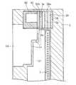
周知のとおり、この種の画像読み取り装置は、一般的には、合成樹脂製のケースに所定の必要な部品を組み付けて構成されている(たとえば、特許文献1参照)。図7および図8は、このような従来の画像読み取り装置の一例を示している。図示された画像読み取り装置Bは、透明カバー102を上面部に装着したケース101と、このケース101の底部に組み付けられた帯板状の基板103とを有している。ケース101には、リフレクタ106に保持された導光体105と、レンズアレイ107とが組み付けられている。基板103には、光源104と、基板101の長手方向に列状に並ぶセンサICチップ108とが設けられている。光源104から発せられた光は、導光体105を通過した後に透明カバー102を介して原稿Pに照射されて反射し、その反射光は、レンズアレイ107を通過して複数のセンサICチップ108に造り込まれた複数の受光素子(図示略)上において集束するように構成されている。各受光素子からはその受光量に対応した出力レベルの画像信号が出力され、これらの信号に基づいた処理を行なうことにより、読み取り画像が得られるようになっている。 As is well known, this type of image reading apparatus is generally configured by assembling predetermined necessary parts to a synthetic resin case (see, for example, Patent Document 1). 7 and 8 show an example of such a conventional image reading apparatus. The illustrated image reading apparatus B includes a
この画像読み取り装置Bにおいて、ケース101の底部の周縁には、下方に突出する周壁部101aが形成されており、基板103は、周壁部101aの内側の凹部101bに嵌入させることによりケース101に組み付けられている。この周壁部101aは、ケース101外部の光や異物がケース101と基板103との間を通じてケース101内に侵入することを防止する機能を有している。基板103の長手方向一端部には、コネクタ109が設けられている。このコネクタ109は、基板103を所望の外部機器と接続するためのものであり、基板103の一方の長手縁部からその一部が突出するように設けられている。このため、周壁部101aのコネクタ109に対応する部分には切欠部101dが形成されており、ケース101に基板103を組み付ける際のコネクタ109と周壁部101aとの干渉が回避されている。 In this image reading apparatus B, a peripheral wall portion 101a that protrudes downward is formed at the periphery of the bottom portion of the
ここで、切欠部101dは、コネクタ109との干渉を確実に回避するため、あるいは大きさの異なる複数種類のコネクタに対して汎用性を持たせるためなどの理由により、一般的にはコネクタとの干渉部分よりも大きいサイズで形成される。そうすると、基板103をケース101に組み付けた状態では、切欠部101dとコネクタ109との間に比較的大きな隙間c1が生じることとなり、この隙間c1を通じてケース101外部からの光や異物の侵入が許容される。このため、図8に表われているように、ケース101には、切欠部101dに対して受光素子寄りで、かつ切欠部101dに対応する位置に、下方に突出する隔壁部101eを一体形成して、ケース101内の受光素子側に光や異物が侵入するのを防止していた。 Here, the
ところで、上記画像信号は、電気的なノイズの影響を受けやすく、このノイズが画像信号中に混入して、読み取り画像の質が悪くなる場合があった。このため、ノイズ対策として、ケース101に導電性を持たせるとともに、このケース101を、基板103を利用してグランド接続することにより、ケース101の帯電防止が図られる場合がある。図9はこのような場合の具体例を示している。ケース101は、たとえばポリカーボネートにカーボンファイバーを含有させたものであり、導電性を有している。基板103の表面およびケース101の隔壁部101eの下端面には、たとえば導電性に優れる銀ペーストを塗布することにより電極110A,110Bが形成されている。電極110Aは、基板103上に設けられた配線(図示略)に繋がっているとともに、電極110A上には、半田バンプ111が設けられている。基板103は、電極110A上の半田バンプ111がケース101側の電極110Bに接触する状態でケース101に組み付けられている。 By the way, the image signal is easily affected by electrical noise, and this noise may be mixed in the image signal and the quality of the read image may deteriorate. For this reason, as a countermeasure against noise, the
ここで、ケース101の表面には樹脂成分が多く析出しているため、図9に示す構成と異なり、半田バンプ111をケース101の表面に直接接触させただけでは、ケース101と半田バンプ111との電気的な導通を図ることができない。そこで、図9に示すように、良導電性の電極110Bを半田バンプ111との接触領域よりも大きい領域に形成して半田バンプ111を電極110Bに接触させると、電極110Bを介してケース101と半田バンプ111との導通を充分に得ることができる。これにより、ケース101は、電極110A,110Bおよび半田バンプ111を介して基板103と電気的に導通することとなり、グランド接続される。したがって、ケース101は過剰に帯電することがなく、画像信号中にノイズが混入することは防止される。 Here, since many resin components are deposited on the surface of the
しかしながら、上記のような構成によると、半田バンプ111が電極110Bに接触して擦れることにより、電極110Bに含まれる銀粒子が発塵し、周囲に飛散する場合がある。また、電極110A,110Bにおいては、溶剤の揮発などに起因して密着力が低下し、電極110A,110Bの表面から自然に発塵した銀粒子が飛散する場合もある。そして、この飛散した銀粒子が受光素子上に付着すると、受光素子において光を適正に感知することができず、読み取り画像の質が悪くなってしまう。 However, according to the above configuration, when the
本発明は、上記した事情のもとで考え出されたものであって、導電性を有するケースと、ケースに形成された電極とを備えた画像読み取り装置において、ケースの帯電防止を適切に図りつつ、受光素子上への導電粒子の付着を回避し、適正な読み取り画像を得ることができる画像読み取り装置を提供することを課題としている。 The present invention has been conceived under the circumstances described above, and in an image reading apparatus including a conductive case and an electrode formed on the case, the case can be appropriately prevented from being charged. On the other hand, an object of the present invention is to provide an image reading apparatus capable of avoiding adhesion of conductive particles on a light receiving element and obtaining an appropriate read image.
上記課題を解決するため、本発明では、次の技術的手段を講じている。 In order to solve the above problems, the present invention takes the following technical means.
本発明によって提供される画像読み取り装置は、導電性を有するケースと、上記ケースの底部に組み付けられる基板と、上記ケースの内部に収容可能であり、かつ上記基板上に設けられた画像読み取り用の複数の受光素子と、上記ケースに形成された第1の電極と、上記基板上に設けられた第2の電極と、を備えている画像読み取り装置であって、上記ケースには、収容凹部が形成されており、上記収容凹部には、上記第1の電極の表面を覆うように上記第1の電極と接触し、かつ上記第2の電極と接触することにより、上記第1および第2の電極を離隔させつつ上記第1および第2の電極を電気的に導通させる導電コンタクト部材が収容されていることを特徴としている。Image reading apparatus which isto the onsetMing Thus provided, a case having a conductive, a substrate is assembled to the bottom of the case, it can be accommodated in the interior of the case, and an image reading provided on the substrate An image reading apparatus comprising a plurality of light receiving elements for use, a first electrode formed on the case, and a second electrode provided on the substrate, wherein the case accommodates A recess is formed, and the housing recess is in contact with the first electrode and the second electrode so as to cover the surface of the first electrode. A conductive contact member that electrically connects the first and second electrodes while separating the two electrodes is housed.
このような構成によれば、第1の電極に対し、この第1の電極を覆うようにして導電コンタクト部材が接触するため、第1の電極の導電粒子が発塵することは抑制される。また、第1の電極の表面は導電コンタクト部材で覆われているため、何らかの原因で第1の電極の導電粒子が発塵する場合でも、その導電粒子が飛散することはなく、基板上に設けられた受光素子上に第1の電極の導電粒子が付着することは適切に回避される。したがって、本発明によれば、適正な読み取り画像を得ることができる。 According to such a configuration, since the conductive contact member comes into contact with the first electrode so as to cover the first electrode, generation of dust from the conductive particles of the first electrode is suppressed. Further, since the surface of the first electrode is covered with the conductive contact member, even if the conductive particles of the first electrode generate dust for some reason, the conductive particles are not scattered and provided on the substrate. Adhering of the conductive particles of the first electrode on the received light receiving element is appropriately avoided. Therefore, according to the present invention, an appropriate read image can be obtained.
上記構成によれば、ケースの表面に形成された第1の電極と基板上に設けられた第2の電極とが導電コンタクト部材を介して電気的に導通するため、基板を利用してケースをグランド接続することができる。したがって、ケースは過剰に帯電することがなく、画像信号中にノイズが混入することは防止される。 According to the above configuration, the first electrode formed on the surface of the case and the second electrode provided on the substrate are electrically connected via the conductive contact member. Can be connected to ground. Therefore, the case is not excessively charged, and noise is prevented from being mixed in the image signal.
また、上記構成によれば、ケースの収容凹部に導電コンタクト部材を収容することによってケースに対する導電コンタクト部材の位置決めがなされるため、導電コンタクト部材をケースに取り付ける際に、取り付け作業の容易化を図ることができる。 Further, according to the above configuration, the conductive contact member is positioned with respect to the case by housing the conductive contact member in the housing recess of the case. Therefore, when the conductive contact member is mounted on the case, the mounting work is facilitated. be able to.
本発明の好ましい実施の形態においては、上記第1の電極は、少なくとも上記収容凹部の底面部上に形成されている。 In a preferred embodiment of the present invention, the first electrode is formed on at least the bottom surface of the housing recess.
このような構成によれば、基板をケースに組み付けた状態において導電コンタクト部材は、収容凹部の底面部と基板上に設けられた第2の電極とに上下方向から押圧されて挟まれた格好となるが、第1の電極が収容凹部の底面部上に形成されているため、導電コンタクト部材を介しての第1の電極と第2の電極との導通接続を確実なものとすることができる。 According to such a configuration, in a state where the substrate is assembled to the case, the conductive contact member is pressed and sandwiched between the bottom surface portion of the housing recess and the second electrode provided on the substrate. However, since the first electrode is formed on the bottom surface of the housing recess, the conductive connection between the first electrode and the second electrode via the conductive contact member can be ensured. .
本発明の好ましい実施の形態においては、上記導電コンタクト部材は、導電ゴム製である。 In a preferred embodiment of the present invention, the conductive contact member is made of conductive rubber.
このような構成によれば、導電コンタクト部材は弾性を有するため、第1の電極や第2の電極に対して導電コンタクト部材を面接触させることができる。したがって、導電コンタクト部材と第1の電極や第2の電極との接触面積を大きくすることが可能となり、導電コンタクト部材を介しての第1の電極と第2の電極との導通接続を確実にするうえでより好ましいものとなる。 According to such a configuration, since the conductive contact member has elasticity, the conductive contact member can be brought into surface contact with the first electrode or the second electrode. Therefore, the contact area between the conductive contact member and the first electrode or the second electrode can be increased, and the conductive connection between the first electrode and the second electrode through the conductive contact member is ensured. This is more preferable.
本発明の好ましい実施の形態においては、上記導電コンタクト部材の上下方向の少なくとも一方の面は、凹凸状に形成されている。 In a preferred embodiment of the present invention, at least one surface of the conductive contact member in the vertical direction is formed in an uneven shape.
このような構成によれば、第1の電極や第2の電極の厚みにバラつきが生じても、導電コンタクト部材の凹凸状に形成された面の凸部が傾倒することにより、このバラツキを吸収することができる。したがって、基板がケースに対して浮き上がった状態で組み付けられることがなく、読み取り画像の質を高めることができる。 According to such a configuration, even if variations occur in the thicknesses of the first electrode and the second electrode, the unevenness of the surface of the conductive contact member that is formed in an uneven shape is tilted to absorb this variation. can do. Therefore, the quality of the read image can be improved without being assembled in a state where the substrate is lifted from the case.
本発明の好ましい実施の形態においては、上記収容凹部の底面部には、突起部が形成されている。 In preferable embodiment of this invention, the projection part is formed in the bottom face part of the said accommodation recessed part.
このような構成によれば、ケースに含まれるカーボンファイバーは上記突起部の表面に露出しやすくなる。したがって、ケースと電極との導通を確保するうえで有利となる。 According to such a configuration, the carbon fiber contained in the case is easily exposed on the surface of the protrusion. Therefore, it is advantageous in securing the conduction between the case and the electrode.
本発明の好ましい実施の形態においては、上記収容凹部は、上記複数の受光素子が収容される上記ケースの内部領域との間を隔壁によって実質的に仕切られている。 In a preferred embodiment of the present invention, the housing recess is substantially partitioned by a partition wall from an inner region of the case in which the plurality of light receiving elements are housed.
このような構成によれば、収容凹部の底面部上に形成された第1の電極は、受光素子が収容されるケースの内部領域に対し、隔壁によって仕切られることとなる。したがって、受光素子上に第1の電極の導電粒子が付着することをより確実に回避することができ、適正な読み取り画像を得るうえでより好ましいものとすることができる。 According to such a structure, the 1st electrode formed on the bottom face part of an accommodation recessed part will be partitioned off with a partition with respect to the internal area | region of the case in which a light receiving element is accommodated. Therefore, it is possible to more reliably avoid the conductive particles of the first electrode from adhering to the light receiving element, which can be more preferable in obtaining an appropriate read image.
本発明のその他の特徴および利点については、以下に行なう発明の実施の形態の説明から、より明らかになるであろう。 Other features and advantages of the present invention will become more apparent from the following description of the embodiments of the invention.
以下、本発明の好ましい実施の形態について、図面を参照して具体的に説明する。 Hereinafter, preferred embodiments of the present invention will be specifically described with reference to the drawings.
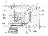
図1〜図5は、本発明に係る画像読み取り装置の一例を示している。本実施形態の画像読み取り装置Aは、たとえばプラテンローラRによって原稿送りがなされるスキャナの構成部品として用いられるものであり、ケース1、透明カバー2、基板3、光源4、導光体5、リフレクタ6、レンズアレイ7、複数のセンサICチップ8、コネクタ9、第1の電極としての電極10、第2の電極としての半田バンプ11、および導電コンタクト部材20を具備して構成されている。 1 to 5 show an example of an image reading apparatus according to the present invention. The image reading apparatus A according to the present embodiment is used as, for example, a component of a scanner that is fed by a platen roller R, and includes a
ケース1は、たとえばポリカーボネートにカーボンファイバーを7〜10重量%程度含有させた合成樹脂製であり、主走査方向に延びた箱型状とされている。このような材料を用いれば、ケース1は、成形性が良好であるとともに、導電性を有するものとなる。 The
透明カバー2は、たとえば平面視形状が細長矩形状のガラス板または合成樹脂板であり、ケース1の上面開口部を閉塞するようにケース1の上面部に装着されている。 The
レンズアレイ7は、主走査方向に延びる細長なブロック状の合成樹脂製のホルダ71に複数のレンズ72を列状に配置させて保持させたものであり、各レンズ72としては、たとえばロッドレンズが用いられている。このレンズアレイ7は、透明カバー2の裏面に対向するようにしてケース1に組み付けられている。 The
光源4は、たとえばR、G、Bの各色の光を発する3種類のLEDチップを一纏めに樹脂パッケージしたものであり、基板3の長手方向一端部の表面に実装されている。 The light source 4 is, for example, a resin package of three types of LED chips that emit light of each color of R, G, and B, and is mounted on the surface of one end portion in the longitudinal direction of the
導光体5は、光源4から発せられた光を透明カバー2の原稿読み取り領域Sの全域に効率よく導くためのものであり、ケース1の長手方向に延びるブロック状を呈している。この導光体5は、たとえばPMMAなどのアクリル系透明樹脂やその他の光透過性に優れる部材により形成されており、各所の表面はすべて鏡面とされている。導光体5の下面には複数の凹部(図示略)が長手方向に所定の間隔を隔てて設けられている。導光体5内を進行する光が上記各凹部に入射すると、その光は種々の方向に散乱反射することとなり、光出射面5aから画像読み取り領域Sに向けて出射することが可能となる。 The
リフレクタ6は、導光体5の全長寸法に略対応した全長寸法を有する第1部材61および第2部材62から構成されており、これらの間で導光体5を挟み込むことにより導光体5を保持するようになっている。第1および第2部材61,62は、光源4から発せられた光が導光体5の外部に不当に漏れることを防止するために、たとえば白色の樹脂により形成され、光反射率の高いものとされている。第1および第2部材61,62には、導光体5を嵌入可能なリフレクト面61a,62aが形成されており、光源4から発せられた光は、導光体5の各所表面での全反射あるいはリフレクト面61a,62aでの反射を繰り返して進行し、導光体5の光照射面5aから原稿読み取り領域Sに向けて照射される。リフレクタ6は、導光体5を一体的に保持した状態でケース1に組み付けられている。 The
複数のセンサICチップ8は、複数の受光素子81を備えた集積回路が造り込まれた半導体チップであり、主走査方向(基板3の長手方向)に繋がって列状に並ぶように基板3の表面に実装されている。複数のセンサICチップ8は、基板3がケース1の底部に取り付けられることにより、ケース1の内部領域1rに収容されるとともに、レンズアレイ7を通過してきた光を各受光素子81で受光できるようになっている。各受光素子81は、光電変換機能を有するものであり、所定の受光面に光を受けると、その受光量に対応したレベルの信号(画像信号)を出力するように構成されている。 The plurality of
基板3は、たとえばセラミック製の帯板状であり、その長手方向一端部には基板3を所望の外部機器と接続するためのコネクタ9が設けられている。この基板3の表面には、コネクタ9と光源4や複数のセンサICチップ8とを電気的に導通させるための配線(図示略)が設けられている。光源4への電力供給および複数のセンサICチップ8への各種信号の入出力は上記配線とコネクタ9とを介して行なわれる。 The
基板3は、ケース1の底部開口部を閉塞するようにケース1の底部に組み付けられている。具体的には、ケース1の底部の周縁には、下方に突出する周壁部1aが形成されており、基板3は、周壁部1aの内側の凹部1bに嵌入させることによりケース1に組み付けられている。凹部1bの底面1cは平面状とされている、基板3の表面が底面1cに当接することにより、ケース1外部の光や塵・埃などの異物がケース1と基板3との間を通じてケース1の内部領域1rに侵入することが防止される。 The
図1、図4および図5に表われているように、周壁部1aのコネクタ9に対応する部分には切欠部1dが形成されており、ケース1に基板3を組み付ける際のコネクタ9と周壁部1aとの干渉が回避されている。切欠部1dは、コネクタ9との干渉部分よりも大きいサイズとして形成される。したがって、基板3をケース1に組み付けた状態では、切欠部1dとコネクタ9との間に比較的大きな隙間c1が生じている。ケース1には、切欠部1dに対して受光素子81寄りで、かつ切欠部1dに対応する位置に、下方に突出する隔壁部1eが一体形成されている。隔壁部1eの下端面1fは、凹部1bの底面1cと面一の平面状とされている。 As shown in FIGS. 1, 4, and 5, a
基板3の表面におけるケース1と当接する位置(凹部1bの底面1cおよび隔壁部1eの下端面1fと対向する位置)には、絶縁膜(図示略)が形成されている。この絶縁膜は、たとえばシリカ系無機充填剤と溶剤を混入したエポキシ樹脂系のレジスト膜により構成されている。 An insulating film (not shown) is formed on the surface of the
図3および図5に表われているように、ケース1の長手方向一端側の底部には、導電コンタクト部材20を収容するための底面視矩形状の収容凹部1gが形成されている。収容凹部1gは、底面部1hおよび四方の側面部1k,1m,1n,61bで囲まれることにより形成されており、内部領域1rとの間を隔壁部1eによって仕切られるように配置されている。ここで、側面部61bは、リフレクタ6の第1部材61の表面である。このように、収容凹部を囲むための側面部は、ケース1以外の部材の表面を利用して構成されているが、収容凹部を囲むための側面部のすべてがケース1の表面により構成されていてもよい。底面部1hには、ケース1の長手方向に沿って延びる複数の突起部1pが形成されている。底面部1h上には、電極10が形成されている。電極10は、たとえば銀ペーストを塗布することにより形成されたものである。上記銀ペーストは、銀粒子を樹脂バインダーに混入し、さらに有機系樹脂と溶剤からなる粘性媒体に混ぜてペースト状にしたものである。 As shown in FIGS. 3 and 5, a housing recess 1 g having a rectangular shape in a bottom view for housing the
ケース1の収容凹部1gには、導電コンタクト部材20が収容されている。この導電コンタクト部材20は、たとえばシリコーンゴムにカーボンファイバーを20〜60重量%程度含有させたものであり、導電性を有するいわゆる導電ゴム製である。図6に示すように、導電コンタクト部材20は、直方体の上面および下面において複数の凸部20aを有する凹凸状に形成された形状であり、上下対称形状とされている。導電コンタクト部材20の厚みtは、収容凹部1gの深さdよりも僅かに大きい寸法とされており、導電コンタクト部材20の幅w1は、収容凹部1gの幅w2よりも僅かに大きい寸法とされている。 A
基板3の表面には、半田バンプ11が形成されている。半田バンプ11は、収容凹部1fに対向する位置において基板3の上方へ突出した突起状に形成されている。半田バンプ11は、上記基板3上の配線に繋がっており、グランドの電位に設定されている。図3によく表われているように、ケース1に基板3が組み付けられると、導電コンタクト部材20は、収容凹部1gの底面部1hと基板3の表面ないし半田バンプ11との間で押圧されて挟まれることにより、底面部1h上に形成された電極10、および半田バンプ11と面接触する。これにより、ケース1は、電極10、導電コンタクト部材20および半田バンプ11を介して基板3と導通し、グランド接続される。 Solder bumps 11 are formed on the surface of the
次に、画像読み取り装置Aの作用について説明する。 Next, the operation of the image reading apparatus A will be described.
まず、光源4を発光させると、その光は導光体5に導かれ、導光体5の各所表面での全反射あるいはリフレクタ6のリフレクト面61a,62aでの反射を繰り返して進行し、導光体5の光照射面5aから原稿読み取り領域Sに向けて照射される。すると、画像読み取り領域S上の原稿Pの表面で反射した光はレンズアレイ7の各レンズ71を通過して、センサICチップ8に造り込まれた各受光素子81によって受光される。これにより、複数の受光素子81上には原稿Pの画像が結像されることとなり、各受光素子81から出力される画像信号が処理されて読み取り画像が得られる。 First, when the light source 4 emits light, the light is guided to the
本実施形態においては、従来技術と異なり、基板3上に設けられた半田バンプ11がケース1に形成された電極10に直接接触することがなく、電極10に対し、電極10を覆うようにして導電コンタクト部材20が接触するため、電極10に含まれる銀粒子が発塵することは抑制される。一方、電極10においては、上記銀ペーストに含まれていた溶剤の揮発などに起因して密着力が低下し、電極10の表面から銀粒子が発塵する場合がある。このように銀粒子が発塵する場合でも、導電コンタクト部材20は電極10の表面を覆うように設けられているため、銀粒子が飛散することはなく、基板3上に設けられた受光素子81上に銀粒子が付着することは適切に回避される。その結果、適正な読み取り画像を得ることができる。 In this embodiment, unlike the prior art, the
また、上述したように、ケース1はグランド接続されているため、ケース1が過剰に帯電することはなく、画像信号中にノイズが混入することは適切に防止される。 As described above, since the
本実施形態においては、ケース1の収容凹部1gに導電コンタクト部材20が収容されている。これにより、ケース1に対する導電コンタクト部材20の位置決めがなされるため、導電コンタクト部材20をケース1に取り付ける際に、取り付け作業の容易化を図ることができる。また、基板3をケース1に組み付けた状態において、導電コンタクト部材20は、収容凹部1gの底面部1hと半田バンプ11とに上下方向から押圧されて挟まれた格好となるが、電極10が収容凹部1gの底面部1h上に形成されているため、導電コンタクト部材20を介しての電極10と半田バンプ11との導通接続を確実なものとすることができる。 In the present embodiment, the
とくに、導電コンタクト部材20は、導電ゴム製で弾性を有するため、収容凹部1gの底面部1hと基板3の表面ないし半田バンプ11との間で押圧されて挟まれることにより、電極10や半田バンプ11に対して面接触することができる。したがって、導電コンタクト部材20と電極10や半田バンプ11との接触面積を大きくすることが可能となり、導電コンタクト部材20を介しての電極10と半田バンプ11との導通接続を確実にするうえでより好ましいものとなる。 In particular, since the
さらに、導電コンタクト部材20の上面および下面は凹凸状に形成されているため、基板3をケース1に組み付ける際には、上記上面および下面の凸部20aが圧縮されながら傾倒し、基板3の表面をケース1の底面1cおよび隔壁部1の下端面1fに当接させることができる。すなわち、半田バンプ11や電極10の厚みにバラつきが生じても、凸部20aが傾倒することにより、このバラつきを吸収することができる。したがって、基板3がケース1に対して浮き上がった状態で組み付けられることがなく、読み取り画像の質を高めることができる。なお、導電コンタクト部材20は上下対称形状とされているため、導電コンタクト部材20をケース1に取り付ける際に導電コンタクト部材20の上下面の向きを考慮する必要がなく、好都合である。 Furthermore, since the upper and lower surfaces of the
また、前述したように、基板3の表面におけるケース1と当接する位置には絶縁膜が形成されているため、ケース1が基板3上の導体部分と不当に導通することがなく、画像読み取り装置Aが誤動作することは、適切に防止される。 Further, as described above, since the insulating film is formed at the position where the surface of the
本実施形態においては、収容凹部1gは、複数の受光素子81が収容されるケース1の内部領域1rとの間を隔壁部1eによって仕切られている。すなわち、収容凹部1gの底面部1h上に形成された電極10は、受光素子が収容された内部領域1rに対し、隔壁部1eによって仕切られることとなる。したがって、受光素子81上に電極10の導電粒子が付着することをより確実に回避することができ、適正な読み取り画像を得るうえでより好ましいものとすることができる。 In the present embodiment, the housing recess 1g is partitioned by the partition wall portion 1e from the internal region 1r of the
本実施形態においては、収容凹部1gの底面部1hには、突起部1pが形成されているため、ケース1に含まれるカーボンファイバーは突起部1pの表面に露出しやすくなる。したがって、ケース1と電極10との導通を確保するうえで有利となる。 In the present embodiment, since the protruding
以上、本発明の具体的な実施形態を説明したが、本発明はこれに限定されるものではなく、発明の思想から逸脱しない範囲内で種々の変更が可能である。 While specific embodiments of the present invention have been described above, the present invention is not limited to these embodiments, and various modifications can be made without departing from the spirit of the invention.
上記実施形態において、収容凹部1gは底面視矩形状に形成されているが、収容凹部の形状はこれに限定されるものではない。収容凹部は、たとえば底面視円形状など上記実施形態とは異なる形状とすることができる。 In the said embodiment, although the accommodation recessed part 1g is formed in the bottom view rectangular shape, the shape of an accommodation recessed part is not limited to this. The housing recess can have a shape different from that of the above embodiment, for example, a circular shape in a bottom view.
本発明における導電コンタクト部材の材質や形状は、上記実施形態に限定されるものではなく、適宜変更が可能である。 The material and shape of the conductive contact member in the present invention are not limited to the above embodiment, and can be changed as appropriate.
上記実施形態における画像読み取り装置Aは、プラテンローラによって原稿送りがなされるスキャナに組み付けられて用いられる例であるが、これに限定されるものではない。本発明に係る画像読み取り装置は、いわゆるフラットベッドタイプのスキャナやハンディスキャナなど画像読み取りがなされる種々の機器に組み付けるなどして広く用いることができる。 The image reading apparatus A in the above embodiment is an example used by being assembled in a scanner that is fed by a platen roller, but is not limited to this. The image reading apparatus according to the present invention can be widely used by being assembled in various devices such as a so-called flatbed type scanner and a handy scanner that can read an image.
A 画像読み取り装置
1 ケース
1e 隔壁部(隔壁)
1g 収容凹部
1h 底面部
1p 突起部
1r 内部領域
3 基板
10 電極(第1の電極)
11 半田バンプ(第2の電極)
20 導電コンタクト部材
81 受光素子A
11 Solder bump (second electrode)
20
Claims (6)
Translated fromJapanese上記ケースには、収容凹部が形成されており、
上記収容凹部には、上記第1の電極の表面を覆うように上記第1の電極と接触し、かつ上記第2の電極と接触することにより、上記第1および第2の電極を離隔させつつ上記第1および第2の電極を電気的に導通させる導電コンタクト部材が収容されていることを特徴とする、画像読み取り装置。A conductive case, a substrate assembled to the bottom of the case, a plurality of light receiving elements for image reading that can be accommodated inside the case and provided on the substrate, and formed on the case An image reading apparatus comprising: a first electrode; and a second electrode provided on the substrate,
The case has a housing recess,
The housing recess is in contact with the first electrode so as to cover the surface of the first electrode, and in contact with the second electrode, thereby separating the first and second electrodes. An image reading apparatus comprising a conductive contact member for electrically connecting the first and second electrodes.
Priority Applications (5)
| Application Number | Priority Date | Filing Date | Title |
|---|---|---|---|
| JP2004319242AJP4440749B2 (en) | 2004-11-02 | 2004-11-02 | Image reading device |
| US11/666,643US7550714B2 (en) | 2004-11-02 | 2005-10-28 | Image reading device |
| CN200580037635ACN100591087C (en) | 2004-11-02 | 2005-10-28 | image reading device |
| PCT/JP2005/019876WO2006049094A1 (en) | 2004-11-02 | 2005-10-28 | Image reading device |
| TW094138287ATW200623833A (en) | 2004-11-02 | 2005-11-01 | Image reading apparatus |
Applications Claiming Priority (1)
| Application Number | Priority Date | Filing Date | Title |
|---|---|---|---|
| JP2004319242AJP4440749B2 (en) | 2004-11-02 | 2004-11-02 | Image reading device |
Publications (2)
| Publication Number | Publication Date |
|---|---|
| JP2006135403A JP2006135403A (en) | 2006-05-25 |
| JP4440749B2true JP4440749B2 (en) | 2010-03-24 |
Family
ID=36319105
Family Applications (1)
| Application Number | Title | Priority Date | Filing Date |
|---|---|---|---|
| JP2004319242AExpired - Fee RelatedJP4440749B2 (en) | 2004-11-02 | 2004-11-02 | Image reading device |
Country Status (5)
| Country | Link |
|---|---|
| US (1) | US7550714B2 (en) |
| JP (1) | JP4440749B2 (en) |
| CN (1) | CN100591087C (en) |
| TW (1) | TW200623833A (en) |
| WO (1) | WO2006049094A1 (en) |
Families Citing this family (13)
| Publication number | Priority date | Publication date | Assignee | Title |
|---|---|---|---|---|
| US9695267B2 (en)* | 2009-08-11 | 2017-07-04 | Honeywell International Inc. | Foams and foamable compositions containing halogenated olefin blowing agents |
| JP5483153B2 (en)* | 2009-03-16 | 2014-05-07 | 株式会社リコー | Light irradiation apparatus, image reading apparatus, and image forming apparatus |
| KR20150005113A (en)* | 2013-07-04 | 2015-01-14 | 에스케이하이닉스 주식회사 | Semiconductor package with optical signal path |
| US9692922B2 (en)* | 2015-03-20 | 2017-06-27 | Fuji Xerox Co., Ltd. | Image reading substrate, image reading device, and image forming apparatus having equal distances of interconnects from output terminals to high-speed serial transmitting unit |
| JP1553847S (en)* | 2015-06-18 | 2016-07-11 | ||
| JP1553414S (en)* | 2015-06-18 | 2016-07-11 | ||
| JP1553417S (en)* | 2015-06-18 | 2016-07-11 | ||
| JP1553848S (en)* | 2015-06-18 | 2016-07-11 | ||
| JP1553413S (en)* | 2015-06-18 | 2016-07-11 | ||
| JP1553845S (en)* | 2015-06-18 | 2016-07-11 | ||
| JP1553846S (en)* | 2015-06-18 | 2016-07-11 | ||
| JP1553412S (en)* | 2015-06-18 | 2016-07-11 | ||
| CN107546508B (en)* | 2016-06-28 | 2019-12-27 | 富士康(昆山)电脑接插件有限公司 | Card edge connector |
Family Cites Families (12)
| Publication number | Priority date | Publication date | Assignee | Title |
|---|---|---|---|---|
| US4694266A (en)* | 1986-07-29 | 1987-09-15 | R. F. Monolithic, Inc. | Notch filter |
| JPH06217078A (en)* | 1993-01-13 | 1994-08-05 | Rohm Co Ltd | Image sensor |
| GB2305096B (en)* | 1995-08-29 | 1997-09-10 | Simage Oy | Imaging system and method |
| GB2315157B (en)* | 1996-07-11 | 1998-09-30 | Simage Oy | Imaging apparatus |
| WO2000030252A1 (en)* | 1998-11-13 | 2000-05-25 | Matsushita Electric Industrial Co., Ltd. | Surface acoustic wave filter |
| US6493033B1 (en)* | 1998-12-09 | 2002-12-10 | Eastman Kodak Company | Electronic apparatus adapted to receive a memory card |
| EP1150488B1 (en)* | 1999-01-26 | 2009-10-07 | Rohm Co., Ltd. | Linear light source and image reading device provided with this |
| CN1189012C (en)* | 2000-07-18 | 2005-02-09 | 松下电器产业株式会社 | Image processor, its image reader and fiber lens, and method for manufacturing fiber lens |
| CA2363775C (en)* | 2001-11-26 | 2010-09-14 | Vr Interactive International, Inc. | A symmetric, high vertical field of view 360 degree reflector using cubic transformations and method |
| US6924715B2 (en)* | 2002-02-12 | 2005-08-02 | Nortel Networks Limited | Band reject filters |
| JP2004193773A (en)* | 2002-12-09 | 2004-07-08 | Rohm Co Ltd | Image read apparatus and unit used for the same |
| US7199353B2 (en)* | 2004-05-12 | 2007-04-03 | Mason Electric Co. | Optical decoder systems and corresponding methods |
- 2004
- 2004-11-02JPJP2004319242Apatent/JP4440749B2/ennot_activeExpired - Fee Related
- 2005
- 2005-10-28CNCN200580037635Apatent/CN100591087C/ennot_activeExpired - Fee Related
- 2005-10-28WOPCT/JP2005/019876patent/WO2006049094A1/enactiveApplication Filing
- 2005-10-28USUS11/666,643patent/US7550714B2/ennot_activeExpired - Fee Related
- 2005-11-01TWTW094138287Apatent/TW200623833A/ennot_activeIP Right Cessation
Also Published As
| Publication number | Publication date |
|---|---|
| TWI307237B (en) | 2009-03-01 |
| WO2006049094A1 (en) | 2006-05-11 |
| CN100591087C (en) | 2010-02-17 |
| US7550714B2 (en) | 2009-06-23 |
| CN101053246A (en) | 2007-10-10 |
| US20080121783A1 (en) | 2008-05-29 |
| TW200623833A (en) | 2006-07-01 |
| JP2006135403A (en) | 2006-05-25 |
Similar Documents
| Publication | Publication Date | Title |
|---|---|---|
| JP4440749B2 (en) | Image reading device | |
| JP4104064B2 (en) | Image reading device | |
| US7419312B2 (en) | Optical module | |
| CN102563451A (en) | Display apparatus and method of assembling the same | |
| WO2000014949A1 (en) | Image reader | |
| JP4313762B2 (en) | Light guide unit and image reading apparatus having the same | |
| US7538912B2 (en) | Image reading apparatus and circuit board unit used therefor | |
| JPH05328012A (en) | Image sensor | |
| JP3964899B2 (en) | Image reading device | |
| JPH11215302A (en) | Image reader and resin package type light source | |
| JPH11313195A (en) | Image reader | |
| JP6386850B2 (en) | Image sensor head and reader | |
| CN109103743B (en) | Packaging structure and packaging method of laser chip | |
| JP6626935B2 (en) | Image sensor head and reading device | |
| JP4008640B2 (en) | Image reading device | |
| JP3810928B2 (en) | Image reading device | |
| JP2007043237A (en) | Image reading device | |
| JP7229397B2 (en) | Equipment housing, image reading device and capacitance detection device | |
| TWI259811B (en) | Optical write head | |
| JP6563162B1 (en) | Image reading device | |
| JP5000535B2 (en) | Image sensor module | |
| JP2001217992A (en) | Image reader | |
| TWM547221U (en) | Contact image sensor and illuminant module | |
| JPH071650U (en) | Document reader | |
| JP2001230901A (en) | Image reading device |
Legal Events
| Date | Code | Title | Description |
|---|---|---|---|
| A621 | Written request for application examination | Free format text:JAPANESE INTERMEDIATE CODE: A621 Effective date:20071022 | |
| A131 | Notification of reasons for refusal | Free format text:JAPANESE INTERMEDIATE CODE: A131 Effective date:20090825 | |
| A521 | Written amendment | Free format text:JAPANESE INTERMEDIATE CODE: A523 Effective date:20091021 | |
| TRDD | Decision of grant or rejection written | ||
| A01 | Written decision to grant a patent or to grant a registration (utility model) | Free format text:JAPANESE INTERMEDIATE CODE: A01 Effective date:20100105 | |
| A01 | Written decision to grant a patent or to grant a registration (utility model) | Free format text:JAPANESE INTERMEDIATE CODE: A01 | |
| A61 | First payment of annual fees (during grant procedure) | Free format text:JAPANESE INTERMEDIATE CODE: A61 Effective date:20100107 | |
| FPAY | Renewal fee payment (event date is renewal date of database) | Free format text:PAYMENT UNTIL: 20130115 Year of fee payment:3 | |
| R150 | Certificate of patent or registration of utility model | Free format text:JAPANESE INTERMEDIATE CODE: R150 | |
| LAPS | Cancellation because of no payment of annual fees |