JP4437565B2 - Semiconductor integrated circuit device, semiconductor integrated circuit device design method, and recording medium - Google Patents
Semiconductor integrated circuit device, semiconductor integrated circuit device design method, and recording mediumDownload PDFInfo
- Publication number
- JP4437565B2 JP4437565B2JP33561698AJP33561698AJP4437565B2JP 4437565 B2JP4437565 B2JP 4437565B2JP 33561698 AJP33561698 AJP 33561698AJP 33561698 AJP33561698 AJP 33561698AJP 4437565 B2JP4437565 B2JP 4437565B2
- Authority
- JP
- Japan
- Prior art keywords
- circuit
- trimming
- power supply
- reference voltage
- semiconductor integrated
- Prior art date
- Legal status (The legal status is an assumption and is not a legal conclusion. Google has not performed a legal analysis and makes no representation as to the accuracy of the status listed.)
- Expired - Fee Related
Links
Images


Classifications
- G—PHYSICS
- G11—INFORMATION STORAGE
- G11C—STATIC STORES
- G11C11/00—Digital stores characterised by the use of particular electric or magnetic storage elements; Storage elements therefor
- G11C11/21—Digital stores characterised by the use of particular electric or magnetic storage elements; Storage elements therefor using electric elements
- G11C11/34—Digital stores characterised by the use of particular electric or magnetic storage elements; Storage elements therefor using electric elements using semiconductor devices
- G—PHYSICS
- G11—INFORMATION STORAGE
- G11C—STATIC STORES
- G11C5/00—Details of stores covered by group G11C11/00
- G11C5/14—Power supply arrangements, e.g. power down, chip selection or deselection, layout of wirings or power grids, or multiple supply levels
- G11C5/143—Detection of memory cassette insertion or removal; Continuity checks of supply or ground lines; Detection of supply variations, interruptions or levels ; Switching between alternative supplies
- G—PHYSICS
- G11—INFORMATION STORAGE
- G11C—STATIC STORES
- G11C5/00—Details of stores covered by group G11C11/00
- G11C5/14—Power supply arrangements, e.g. power down, chip selection or deselection, layout of wirings or power grids, or multiple supply levels
- G11C5/147—Voltage reference generators, voltage or current regulators; Internally lowered supply levels; Compensation for voltage drops
Landscapes
- Engineering & Computer Science (AREA)
- Power Engineering (AREA)
- Computer Hardware Design (AREA)
- Semiconductor Integrated Circuits (AREA)
- Design And Manufacture Of Integrated Circuits (AREA)
- Semiconductor Memories (AREA)
- For Increasing The Reliability Of Semiconductor Memories (AREA)
- Dram (AREA)
Description
Translated fromJapanese【0001】
【発明の属する技術分野】
本発明は半導体集積回路装置に係り、詳しくは、複数のメモリとロジック回路とを混載したシステムLSIに関する。
【0002】
近年、メモリ・ロジック混載型のシステムLSIの需要が高まっている。このようなLSIでは、更なる低消費電力化や高機能化の要求により、1つのデバイスに複数個のメモリが搭載される。そして、このようなシステムLSIの試験時間を短縮することが求められている。
【0003】
【従来の技術】
図5は、従来のシステムLSIの一例を示す。システムLSI1は、記憶容量が2MBの2つのメモリマクロ2,3、記憶容量が8MBのメモリマクロ4、2つのロジック回路5,6を備え、各回路2〜6はそれぞれチップ上の所定位置に配置される。各メモリマクロ2〜4は、図6に示すように一般的な構成であって、メモリセルアレイ10、ロウデコーダ11、コラムデコーダ12、入出力回路13、入力バッファ回路14、ミキサ15、及び、電源系回路16を備える。メモリマクロ2(,3)とメモリマクロ4は、記憶容量が異なるが基本構成は同じであり、それぞれの回路規模が記憶容量に応じて異なるだけである。
【0004】
前記電源系回路16には、例えば図7に示すような降圧回路20が備えられる。降圧回路20は、トリミング回路21、基準電位発生回路22、制御回路23、及び、電源ドライバ回路24を備える。制御回路23にはイネーブル信号ENが入力され、制御回路23はそのイネーブル信号ENに基づいて電源ドライバ回路24を活性・非活性に切り替える。電源ドライバ回路24は、基準電圧発生回路22からの基準電圧Vrに基づいて、外部電源を降圧した内部電源Vinを生成し、その内部電源Vinをメモリセルアレイ10等の動作電源として供給する。
【0005】
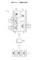
前記トリミング回路21及び基準電圧発生回路22は、図8に示すように構成される。詳述すると、トリミング回路21は、2つのヒューズ回路31,32、及び、4つのAND回路33〜36を備える。
【0006】
ヒューズ回路31は、NMOSトランジスタTr1、ヒューズf01、及び、2つのインバータ回路31a,31bを備える。NMOSトランジスタTr1は、ソースが低電位側電源VSSに接続され、ドレインがヒューズf01を介して高電位側電源VCCに接続される。NMOSトランジスタTr1のドレインは、インバータ回路31aを介して自身のゲートに接続される。そして、NMOSトランジスタTr1のドレインからは、検出信号n01zが出力されるとともに、インバータ回路31bを介して検出信号n01xが出力される。
【0007】
ヒューズ回路32は、NMOSトランジスタTr2、ヒューズf02、及び、2つのインバータ回路32a,32bで構成され、前記ヒューズ回路31と同様に接続される。そして、NMOSトランジスタTr2のドレインからは、検出信号n02zが出力されるとともに、インバータ回路32bを介して検出信号n02xが出力される。
【0008】
前記AND回路33には、検出信号n01x,n02zが入力され、出力端子から各信号n01x,n02zに基づいた出力電圧V1を出力する。前記AND回路34には、検出信号n01z,n02zが入力され、出力端子から各信号n01z,n02zに基づいた出力電圧V2を出力する。前記AND回路35には、検出信号n01z,n02xが入力され、出力端子から各信号n01z,n02xに基づいた出力電圧V3を出力する。前記AND回路36には、検出信号n01x,n02xが入力され、出力端子から各信号n01x,n02xに基づいた出力電圧V4を出力する。そして、AND回路33〜35の出力端子は次段の基準電圧発生回路22に接続される。
【0009】
基準電圧発生回路22は、抵抗R、及び、8つのNMOSトランジスタTr3〜Tr9を備える。電源VCC,VSS間には、抵抗R、及び、4つのNMOSトランジスタTr3〜Tr6が直列に接続される。各NMOSトランジスタTr3〜Tr6は、そのゲートがそれぞれ自身のドレインに接続、即ちダイオード接続される。
【0010】
又、NMOSトランジスタTr3のソースは、NMOSトランジスタTr7を介して低電位側電源VSSに接続される。このNMOSトランジスタTr7のゲートには、前記出力電圧V1が入力される。NMOSトランジスタTr4のソースは、NMOSトランジスタTr8を介して低電位側電源VSSに接続される。このNMOSトランジスタTr8のゲートには、前記出力電圧V2が入力される。NMOSトランジスタTr5のソースは、NMOSトランジスタTr9を介して低電位側電源VSSに接続される。このNMOSトランジスタTr9のゲートには、前記出力電圧V3が入力される。
【0011】
そして、前記NMOSトランジスタTr3のドレインは出力ノードであって、該ノードから前記電源ドライバ回路24に基準電圧Vrを出力するとともに、同基準電圧Vrをチップに設けられた測定用パッドPに出力する。
【0012】
このようなトリミング回路21及び基準電圧発生回路22では、図9に示すように、両ヒューズf01,f02がトリミング処理無しの場合、出力電圧V2のみがHレベルとなる。従って、NMOSトランジスタTr8がオンされ、基準電圧Vrは、電源VCC,VSS間の電位差を、抵抗Rと、ダイオード接続された2つのNMOSトランジスタTr3,Tr4のオン抵抗とで分圧したレベルとなる。
【0013】
又、ヒューズf01のみがトリミング処理がなされた場合、出力電圧V1のみがHレベルとなる。従って、NMOSトランジスタTr7がオンされ、基準電圧Vrは、電源VCC,VSS間の電位差を、抵抗Rと、ダイオード接続された1つのNMOSトランジスタTr3のオン抵抗とで分圧したレベルとなる。
【0014】
又、ヒューズf02のみがトリミング処理がなされた場合、出力電圧V3のみがHレベルとなる。従って、NMOSトランジスタTr9がオンされ、基準電圧Vrは、電源VCC,VSS間の電位差を、抵抗Rと、ダイオード接続された3つのNMOSトランジスタTr3〜Tr5のオン抵抗とで分圧したレベルとなる。
【0015】
更に、両ヒューズf01,f02がトリミング処理がなされた場合、出力電圧V4のみがHレベルとなる。即ち、出力電圧V1〜V3は全てLレベルとなる。従って、NMOSトランジスタTr7〜Tr9がオフ状態に保持され、基準電圧Vrは、電源VCC,VSS間の電位差を、抵抗Rと、ダイオード接続された4つのNMOSトランジスタTr3〜Tr6のオン抵抗とで分圧したレベルとなる。
【0016】
そして、システムLSI1の出荷試験時には、前記測定用パッドPから出力される基準電圧Vrを図示しない測定装置によって測定し、該基準電圧Vrが所定範囲内であるか否かが判定される。このとき、基準電圧Vrが所定範囲内から外れていると、そのずれに応じてヒューズf01,f02のトリミング処理がなされる。基準電圧発生回路22は、各ヒューズf01,f02のトリミング処理の有無の組み合わせに基づいたレベル、即ち略所定の電圧値となる基準電圧Vrを生成する。このようなトリミング処理は各メモリマクロ2〜4毎に同様に行われる。
【0017】
【発明が解決しようとする課題】
ところで、このシステムLSI1をレイアウト設計装置(CAD装置)で設計するにあたり、図5に示すように、ライブラリLbには、上記のメモリマクロ2〜4を含む種々のメモリマクロ、ロジック回路等のライブラリデータが予め登録されている。ライブラリデータは、レイアウトデータ,ネット情報等の各種情報を含む。
【0018】
各メモリマクロは単体で動作可能に構成されている。従って、CAD装置は、ライブラリLbから所望の記憶容量を持つメモリマクロを選択してチップ上に配置するだけで、そのメモリ機能を有するシステムLSIの設計を行うことができる。
【0019】
そのため、システムLSI1にメモリマクロを配置した分だけ(上記では、3つのメモリマクロ2〜4を配置した分だけ)、トリミング回路21が備えられることになる。すると、システムLSI1の出荷試験時において、基準電圧Vrの測定及びトリミング処理がメモリマクロ毎に同様に行われるので、その試験時間が長くなるという問題がある。このような問題は、システムLSIのコストの上昇を招く。
【0020】
又、チップには、各メモリマクロ2〜4の降圧回路20毎に1つの測定用パッドPが必要である。これは、システムLSI1の高集積化の妨げとなる。
尚、これらの問題は、前記降圧回路20に限るものではない。例えば、前記電源系回路16には、前記降圧回路20の他に前記メモリセルアレイ10の基板電位を発生するための基板電位発生回路(図示略)を備えている。基板電位発生回路には、電源ドライバ回路、検知回路、及び、図8と同様なトリミング回路が備えられる。検知回路は、基板電位を検知し、その検知信号を電源ドライバ回路に出力する。電源ドライバ回路は、前記検知信号に基づいた基板電位を生成する。又、前記チップ上には、基板電位を測定するための測定用パッドが設けられている。そして、上記と同様に、測定用パッドから出力される基板電位が測定され、その測定値が所定範囲内から外れていると、該測定値が所定範囲内となるようにトリミング回路内のヒューズをトリミングする。従って、この場合でも、上記と同様の問題が生じる。
【0021】
本発明は、上記問題点を解決するためになされたものであって、その目的は、試験時間を短縮するとともに、高集積化を図ることができる半導体集積回路装置、半導体集積回路装置の設計方法、及び、その半導体集積回路装置のレイアウトデータを記録した記録媒体を提供することにある。
【0022】
【課題を解決するための手段】
請求項1,4,7に記載の発明によれば、半導体集積回路装置に備えられる複数のメモリは、少なくともトリミング回路を含む1つの制御マクロと、前記制御マクロとは別に設けられ、該制御マクロと協働してメモリの機能を提供する複数のメモリユニットとから構成される。また、前記複数のメモリユニットの記憶容量は互いに異なり、前記複数のメモリユニットは前記トリミング回路の前記トリミング処理に基づく前記基準となる信号に基づいて自己の記憶容量に応じた動作電圧を発生する電源ドライバ回路を有する。また、前記複数のメモリユニット間で前記トリミング回路を共用する。従って、トリミング処理を1つの制御マクロに対してのみ行えばよく、各メモリ毎に行う必要がないため、半導体集積回路装置の出荷試験時の試験時間を短縮することができる。又、調整回路の出力信号を測定する測定用パッドを制御マクロに対応して設ければよく、しかも、メモリ間で少なくともトリミング回路が共用されるので、測定用パッド及び回路数を削減することができ、半導体集積回路装置の高集積化を図ることができる。
【0024】
請求項2,5,8に記載の発明によれば、電源ドライバ回路は、基準電圧に基づいて外部電源を昇圧又は降圧した内部電源を生成する回路である。調整回路は、基準電圧を発生し、その基準電圧を電源ドライバ回路に供給する基準電圧発生回路である。トリミング回路は、複数のヒューズを備え、それらヒューズのトリミング処理の有無の組み合わせに基づいて基準電圧を所定範囲内とするヒューズトリミング回路である。
【0025】
請求項3,6,9に記載の発明によれば、電源ドライバ回路は、検知信号のレベルに基づいてメモリセルアレイの基板電位を生成する回路である。調整回路は、基板電位を検知し、その検知結果を検知信号として電源ドライバ回路に出力する検知回路である。トリミング回路は、複数のヒューズを備え、それらヒューズに対して基板電位を所定範囲内とするように施されるトリミング処理の有無の組み合わせに基づく検知信号を出力するヒューズトリミング回路である。
【0026】
【発明の実施の形態】
以下、本発明を具体化した本実施の形態を図1及び図2に従って説明する。尚、説明の便宜上、図5〜8と同様の構成については同一の符号を付してその説明を一部省略する。
【0027】
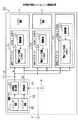
図1は、本実施の形態のシステムLSIの構成を示す。システムLSI51は、記憶容量が2MBの2つのメモリユニット52,53、記憶容量が8MBのメモリユニット54、制御マクロ55、2つのロジック回路5,6を備え、各回路52〜55,5,6はそれぞれチップ上の所定位置に配置されている。
【0028】
図2に示すように、各メモリユニット52〜54は、図6のメモリセルアレイ10、ロウデコーダ11、コラムデコーダ12、入出力回路13、入力バッファ回路14、ミキサ15(何れも図示略)をそれぞれ備えるとともに、降圧回路52a〜54a、基板電位発生回路52b〜54bをそれぞれ備える。降圧回路52a〜54a、基板電位発生回路52b〜54bは同様に構成され、制御回路23と電源ドライバ回路24をそれぞれ備える。
【0029】
制御マクロ55には、複数の降圧回路52a〜54aに対して1組のトリミング回路21及び基準電圧発生回路22が備えられる。基準電圧発生回路22は、各降圧回路52a〜54aの電源ドライバ回路24に接続され、それぞれ基準電圧Vrを出力する。又、制御マクロ55には、複数の基板電位発生回路52b〜54bに対して1組のトリミング回路25及び検知回路26が備えられる。検知回路26は、各基板電位発生回路52b〜54bの電源ドライバ回路24に接続され、それぞれ検知信号SGを出力する。
【0030】
言い換えれば、この形態のシステムLSI51は、各メモリユニット52〜54の降圧回路52a〜54aでトリミング回路21及び基準電圧発生回路22を共用し、基板電位発生回路52b〜54bでトリミング回路25及び検知回路26を共用している。そして、各回路21,22,25,26は、各メモリユニット52〜54とは別の制御マクロ55内に配置される。これは、トリミング回路21,25、基準電圧発生回路22、及び、検知回路26は、各メモリユニット52〜54の記憶容量の大きさに依存されないため、それら回路21,22,25,26が共用化される。尚、各電源ドライバ回路24は、能力が各メモリユニット52〜54の記憶容量の大きさに依存するため、それら能力に応じた回路規模の電源ドライバ回路24が個々のメモリユニット52〜54毎に設けられている。
【0031】
又、基準電圧発生回路22には、基準電圧Vrを測定するためにシステムLSI51のチップ上に設けられた測定用パッドPに接続される。そして、システムLSI51の出荷試験時には、前記測定用パッドPから出力される基準電圧Vrを図示しない測定装置によって測定し、該基準電圧Vrが所定範囲内であるか否かが判定される。このとき、基準電圧Vrが所定範囲内から外れていると、図8に示すようにそのずれに応じてヒューズf01,f02のトリミング処理がなされる。基準電圧発生回路22は、各ヒューズf01,f02のトリミング処理の有無の組み合わせに基づいたレベル、即ち所定電圧値となる基準電圧Vrを生成し、該基準電圧Vrを各降圧回路52a〜54aの電源ドライバ回路24にそれぞれ供給する。こうして、電源ドライバ回路24は、基準電圧Vrに基づいて外部電源を降圧した内部電源Vinを生成する。
【0032】
同様に、検知回路26には、メモリセルアレイ10の基板電位を測定するために同チップ上に設けられた測定用パッドPに接続される。そして、システムLSI51の出荷試験時には、前記測定用パッドPから出力される基板電位を図示しない測定装置によって測定し、該基板電位が所定範囲内であるか否かが判定される。このとき、基板電位が所定範囲内から外れていると、そのずれに応じてヒューズf01,f02のトリミング処理がなされる。検知回路26は、各ヒューズf01,f02のトリミング処理の有無の組み合わせに基づいた検知信号SGを各基板電位発生回路52b〜54bの電源ドライバ回路24にそれぞれ出力する。こうして、各電源ドライバ回路24は、所定電圧値の基板電位を生成し、各メモリセルアレイ10のウェルWに供給する。
【0033】
このように、上記したようなトリミング処理は、制御マクロ55の各トリミング回路21,25にのみ行われる。即ち、3つのメモリユニット52〜54に所定範囲の基準電圧Vrを供給するために、1つのトリミング回路21に対するトリミング処理が行われる。また、3つのメモリユニット52〜54の基板電位を所定範囲とするために、1つのトリミング回路25に対するトリミング処理が行われる。これにより、所定スペックの範囲内に含まれる動作特性を持つシステムLSIが完成される。
【0034】
上記のシステムLSI51のレイアウトデータは、図示しないレイアウト設計装置(CAD装置)を用いて作成される。CAD装置は、図1のライブラリLbを記憶装置に予め格納している。ライブラリLbは、上記構成の2MB,8MBのメモリユニット52〜54を含む種々の記憶容量のメモリユニットのライブラリデータを格納する領域、上記構成の制御マクロ55を含む種々の制御マクロのライブラリデータを格納する領域、等を備える。このライブラリLbは、コンピュータよりなるCAD装置にて読みとり可能な記録媒体(記憶装置を含む)に記録され提供される。
【0035】
CAD装置は、システムLSI51の仕様データに基づいて、ライブラリLbから2M,8Mのメモリユニット52〜54及びそのメモリユニット52〜54に応じた制御マクロ55のライブラリデータを読み出す。そして、CAD装置は、チップ上に各メモリユニット52〜54及び制御マクロ55等を所定の位置に配置し、仕様データ(ネットリスト)に基づいて接続配線のデータを作成する。このようにして、ライブラリLbに格納されたライブラリデータを用いて上記構成のシステムLSI51のレイアウトデータが作成される。
【0036】
上記したように、本実施の形態では、以下に示す作用効果を得ることができる。
(1)この形態のシステムLSI51は、各メモリユニット52〜54の降圧回路52a〜54aで該ユニット52〜54の記憶容量の大きさに依存しないトリミング回路21及び基準電圧発生回路22を共用し、同様に基板電位発生回路52b〜54bでトリミング回路25及び検知回路26を共用している。そして、各回路21,22,25,26は、各メモリユニット52〜54とは別の制御マクロ55内に配置される。従って、基準電圧発生回路22が出力する基準電圧Vrの測定及びトリミング処理と、検知回路26が出力する検知信号SGのレベルの測定及びトリミング処理を単一の制御マクロ55に対してのみ行えばよく、各メモリユニット毎に行う必要がないので、システムLSI51の出荷試験時の試験時間を短縮することができる。
【0037】
(2)トリミング回路21,25、基準電圧発生回路22、及び、検知回路26が共用化されるので、回路数、及び、基準電圧Vr及び検知信号SGのレベルを測定する測定用パッドPの数を削減することができる。従って、システムLSI51の高集積化を図ることができる。
【0038】
尚、本発明の実施の形態は以下のように変更してもよい。
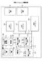
○上記実施の形態では、各電源ドライバ回路24及び制御回路23を各メモリユニット52〜54内に備えたが、図3に示すように、各電源ドライバ回路24及び制御回路23を省略したメモリユニット62〜64と、その各電源ドライバ回路24及びその電源ドライバ回路24で共用化した制御回路23を備える制御マクロ65とで構成してもよい。この場合、制御マクロ65(各電源ドライバ回路24)と各メモリユニット62〜64との間には、各電源ドライバ回路24が生成する内部電源Vinに応じた配線幅の電源配線L1を設ける必要がある。
【0039】
又、図4に示すように、制御マクロ65aを構成してもよい。この制御マクロ65aは、3つの電源ドライバ回路24を、全メモリユニット62〜64に対して内部電源Vinを供給することができる供給能力が高い1つの電源ドライバ回路24aに置換した構成である。この場合、上記と同様に、制御マクロ65a(電源ドライバ回路24a)と各メモリユニット62〜64との間には、電源ドライバ回路24aが生成する内部電源に応じた配線幅の電源配線L2を設ける必要がある。このとき、電源配線L2を各メモリユニット62〜64間でループ状に形成してもよい。
【0040】
更に、前記電源ドライバ回路24aは、全メモリユニット62〜64に対して内部電源Vinを供給することができる供給能力を持つドライバ回路としたが、電源ドライバ回路を、適宜メモリユニットの組み合わせに応じて複数個設けるようにしてもよい。例えば、メモリユニット62,63で1つの電源ドライバ回路を設け、メモリユニット64で1つの電源ドライバ回路を設けるようにしてもよい。
【0041】
○上記実施の形態では、トリミング回路21,25、基準電圧発生回路22、及び、検知回路26を共用化すべく制御マクロ55内に備えたが、各メモリユニット52〜54に共用可能な回路であれば、これらの回路に限定されるものではない。
【0042】
○上記実施の形態では、基準電圧Vrに基づいて外部電源を降圧した内部電源Vinを生成する降圧回路52a〜54aに実施したが、基準電圧Vrに基づいて外部電源を昇圧した内部電源を生成する昇圧回路に実施してもよい。
【0043】
【発明の効果】
以上詳述したように、本発明によれば、試験時間を短縮するとともに、高集積化を図ることができる半導体集積回路装置、半導体集積回路装置の設計方法、及び、その半導体集積回路装置のレイアウトデータを記録した記録媒体を提供することができる。
【図面の簡単な説明】
【図1】 本実施の形態のシステムLSIを説明するための図である。
【図2】 本実施の形態のシステムLSIの概略構成図である。
【図3】 別例のシステムLSIの概略構成図である。
【図4】 別例のシステムLSIの概略構成図である。
【図5】 従来のシステムLSIを説明するための図である。
【図6】 メモリマクロの概略構成図である。
【図7】 降圧回路の概略構成図である。
【図8】 トリミング回路及び基準電圧発生回路の回路図である。
【図9】 トリミング回路を説明するための図である。
【符号の説明】
21,25 トリミング回路
22 調整回路としての基準電圧発生回路
24 電源ドライバ回路
26 調整回路としての検知回路
52〜54 メモリユニット
55 制御マクロ[0001]
BACKGROUND OF THE INVENTION
The present invention relates to a semiconductor integrated circuit device, and more particularly to a system LSI in which a plurality of memories and a logic circuit are mixedly mounted.
[0002]
In recent years, the demand for memory LSI integrated LSIs has increased. In such an LSI, a plurality of memories are mounted in one device due to demands for further lower power consumption and higher functionality. There is a demand for shortening the test time of such a system LSI.
[0003]
[Prior art]
FIG. 5 shows an example of a conventional system LSI. The
[0004]
The power
[0005]
The
[0006]
The
[0007]
The
[0008]
The
[0009]
The reference
[0010]
The source of the NMOS transistor Tr3 is connected to the low potential side power source VSS via the NMOS transistor Tr7. The output voltage V1 is input to the gate of the NMOS transistor Tr7. The source of the NMOS transistor Tr4 is connected to the low potential side power supply VSS via the NMOS transistor Tr8. The output voltage V2 is input to the gate of the NMOS transistor Tr8. The source of the NMOS transistor Tr5 is connected to the low potential side power supply VSS via the NMOS transistor Tr9. The output voltage V3 is input to the gate of the NMOS transistor Tr9.
[0011]
The drain of the NMOS transistor Tr3 is an output node, which outputs the reference voltage Vr from the node to the power
[0012]
In
[0013]
When only the fuse f01 is trimmed, only the output voltage V1 becomes H level. Therefore, the NMOS transistor Tr7 is turned on, and the reference voltage Vr becomes a level obtained by dividing the potential difference between the power sources VCC and VSS by the resistor R and the on-resistance of one diode-connected NMOS transistor Tr3.
[0014]
When only the fuse f02 is trimmed, only the output voltage V3 becomes H level. Accordingly, the NMOS transistor Tr9 is turned on, and the reference voltage Vr becomes a level obtained by dividing the potential difference between the power sources VCC and VSS by the resistor R and the on-resistances of the three diode-connected NMOS transistors Tr3 to Tr5.
[0015]
Further, when both fuses f01 and f02 are trimmed, only the output voltage V4 becomes H level. That is, the output voltages V1 to V3 are all at the L level. Therefore, the NMOS transistors Tr7 to Tr9 are held in the off state, and the reference voltage Vr is obtained by dividing the potential difference between the power sources VCC and VSS by the resistance R and the on resistances of the four diode-connected NMOS transistors Tr3 to Tr6. Level.
[0016]
Then, at the time of a shipment test of the
[0017]
[Problems to be solved by the invention]
By the way, when designing the
[0018]
Each memory macro is configured to operate independently. Therefore, the CAD apparatus can design a system LSI having the memory function only by selecting a memory macro having a desired storage capacity from the library Lb and placing it on the chip.
[0019]
Therefore, the trimming
[0020]
Further, the chip needs one measurement pad P for each step-
These problems are not limited to the step-
[0021]
The present invention has been made in order to solve the above-described problems, and an object of the present invention is to reduce the test time and achieve high integration, and a semiconductor integrated circuit device design method Another object of the present invention is to provide a recording medium on which layout data of the semiconductor integrated circuit device is recorded.
[0022]
[Means for Solving the Problems]
According to the invention of
[0024]
According to the invention described in
[0025]
According to thethird ,sixth, andninth aspects of the invention, the power supply driver circuit is a circuit that generates the substrate potential of the memory cell array based on the level of the detection signal. The adjustment circuit is a detection circuit that detects the substrate potential and outputs the detection result to the power supply driver circuit as a detection signal. The trimming circuit is a fuse trimming circuit that includes a plurality of fuses and outputs a detection signal based on a combination of presence / absence of a trimming process applied to the fuses so that the substrate potential is within a predetermined range.
[0026]
DETAILED DESCRIPTION OF THE INVENTION
Hereinafter, the present embodiment embodying the present invention will be described with reference to FIGS. For convenience of explanation, the same components as those shown in FIGS.
[0027]
FIG. 1 shows the configuration of the system LSI of the present embodiment. The
[0028]
As shown in FIG. 2, each of the
[0029]
The
[0030]
In other words, in the
[0031]
The reference
[0032]
Similarly, the
[0033]
As described above, the trimming process as described above is performed only on the trimming
[0034]
The layout data of the
[0035]
Based on the specification data of the
[0036]
As described above, in the present embodiment, the following operational effects can be obtained.
(1) The
[0037]
(2) Since the trimming
[0038]
In addition, you may change embodiment of this invention as follows.
In the above embodiment, each power
[0039]
Further, as shown in FIG. 4, a control macro 65a may be configured. The control macro 65a has a configuration in which the three power
[0040]
Further, the
[0041]
In the above embodiment, the trimming
[0042]
In the above embodiment, the step-down
[0043]
【The invention's effect】
As described above in detail, according to the present invention, the semiconductor integrated circuit device, the design method of the semiconductor integrated circuit device, and the layout of the semiconductor integrated circuit device that can reduce the test time and achieve high integration. A recording medium on which data is recorded can be provided.
[Brief description of the drawings]
FIG. 1 is a diagram for explaining a system LSI of an embodiment;
FIG. 2 is a schematic configuration diagram of a system LSI of the present embodiment.
FIG. 3 is a schematic configuration diagram of another example of a system LSI.
FIG. 4 is a schematic configuration diagram of another example of a system LSI.
FIG. 5 is a diagram for explaining a conventional system LSI.
FIG. 6 is a schematic configuration diagram of a memory macro.
FIG. 7 is a schematic configuration diagram of a step-down circuit.
FIG. 8 is a circuit diagram of a trimming circuit and a reference voltage generation circuit.
FIG. 9 is a diagram for explaining a trimming circuit;
[Explanation of symbols]
21, 25
Claims (9)
Translated fromJapanese前記トリミング回路を含む1つの制御マクロと、
前記制御マクロとは別に設けられ、該制御マクロと協働して前記メモリの機能を提供する複数のメモリユニットとを有し、
前記複数のメモリユニットの記憶容量は互いに異なり、前記複数のメモリユニットは前記トリミング回路の前記トリミング処理に基づく前記基準となる信号に基づいて自己の記憶容量に応じた動作電圧を発生する電源ドライバ回路を有し、
前記複数のメモリユニット間で前記トリミング回路を共用する半導体集積回路装置。A semiconductor integrated circuit having a plurality of memories having an adjustment circuit that outputs a reference signal to the power supply driver circuit based on a trimming process of a trimming circuit applied so that the operating power generated by the power supply driver circuit is within a predetermined range A circuit device,
One control macro including the trimming circuit;
The control macro The separately provided, and a plurality of memory units that provide the functionality of the memory in cooperation withthe control macro,
The memory capacities of the plurality of memory units are different from each other, and the plurality of memory units generate an operating voltage corresponding to their own memory capacity based on the reference signal based on the trimming process of the trimming circuit.I have a,
A semiconductor integrated circuit devicesharing thetrimming circuit among the plurality of memory units .
前記電源ドライバ回路は、基準電圧に基づいて外部電源を昇圧又は降圧した内部電源を生成する回路であり、 The power supply driver circuit is a circuit that generates an internal power supply by boosting or stepping down an external power supply based on a reference voltage,
前記調整回路は、前記基準電圧を発生し、その基準電圧を前記電源ドライバ回路に供給する基準電圧発生回路であり、 The adjustment circuit is a reference voltage generation circuit that generates the reference voltage and supplies the reference voltage to the power supply driver circuit.
前記トリミング回路は、複数のヒューズを備え、それらヒューズのトリミング処理の有無の組み合わせに基づいて前記基準電圧を所定範囲内とするヒューズトリミング回路であることを特徴とする半導体集積回路装置。 2. The semiconductor integrated circuit device according to claim 1, wherein the trimming circuit is a fuse trimming circuit including a plurality of fuses and setting the reference voltage within a predetermined range based on a combination of presence / absence of trimming processing of the fuses.
前記電源ドライバ回路は、検知信号のレベルに基づいてメモリセルアレイの基板電位を生成する回路であり、 The power supply driver circuit is a circuit that generates a substrate potential of a memory cell array based on a level of a detection signal,
前記調整回路は、前記基板電位を検知し、その検知結果を前記検知信号として前記電源ドライバ回路に出力する検知回路であり、 The adjustment circuit is a detection circuit that detects the substrate potential and outputs the detection result to the power supply driver circuit as the detection signal;
前記トリミング回路は、複数のヒューズを備え、それらヒューズに対して前記基板電位を所定範囲内とするように施されるトリミング処理の有無の組み合わせに基づく前記検知信号を出力するヒューズトリミング回路であることを特徴とする半導体集積回路装置。 The trimming circuit includes a plurality of fuses, and is a fuse trimming circuit that outputs the detection signal based on a combination of presence / absence of trimming processing applied to the fuses so that the substrate potential is within a predetermined range. A semiconductor integrated circuit device.
前記トリミング回路を含む1つの制御マクロのデータと、
前記制御マクロと協働して前記メモリの機能を提供する複数のメモリユニットのデータとに基づいて、前記各メモリユニットと前記制御マクロとをチップ上に別々にレイアウトし、互いを接続して前記複数のメモリを構成し、
前記複数のメモリユニットの記憶容量は互いに異なり、前記複数のメモリユニットは前記トリミング回路の前記トリミング処理に基づく前記基準となる信号に基づいて自己の記憶容量に応じた動作電圧を発生する電源ドライバ回路を有し、前記複数のメモリユニット間で前記トリミング回路を共用することを特徴とする半導体集積回路装置の設計方法。A semiconductor integrated circuit having a plurality of memories having an adjustment circuit that outputs a reference signal to the power supply driver circuit based on a trimming process of a trimming circuit applied so that the operating power generated by the power supply driver circuit is within a predetermined range A circuit device design method comprising:
Data of one control macro including the trimming circuit;
The memory units and the control macro areseparately laid out on a chip based on data of a plurality of memory units that provide the function of the memory in cooperation with the control macro, and connected to each other to connect the control macro. Configure multiple memories
The memory capacities of the plurality of memory units are different from each other, and the plurality of memory units generate an operating voltage corresponding to their own memory capacity based on the reference signal based on the trimming process of the trimming circuit.have a method fordesigning a semiconductor integrated circuit device characterized bysharing the trimming circuit among the plurality of memory units.
前記電源ドライバ回路は、基準電圧に基づいて外部電源を昇圧又は降圧した内部電源を生成する回路であり、 The power supply driver circuit is a circuit that generates an internal power supply by boosting or stepping down an external power supply based on a reference voltage,
前記調整回路は、前記基準電圧を発生し、その基準電圧を前記電源ドライバ回路に供給する基準電圧発生回路であり、 The adjustment circuit is a reference voltage generation circuit that generates the reference voltage and supplies the reference voltage to the power supply driver circuit.
前記トリミング回路は、複数のヒューズを備え、それらヒューズのトリミング処理の有無の組み合わせに基づいて前記基準電圧を所定範囲内とするヒューズトリミング回路であることを特徴とする半導体集積回路装置の設計方法。 The design method of a semiconductor integrated circuit device, wherein the trimming circuit is a fuse trimming circuit having a plurality of fuses and setting the reference voltage within a predetermined range based on a combination of presence / absence of trimming processing of the fuses.
前記電源ドライバ回路は、検知信号のレベルに基づいてメモリセルアレイの基板電位を生成する回路であり、 The power supply driver circuit is a circuit that generates a substrate potential of a memory cell array based on a level of a detection signal,
前記調整回路は、前記基板電位を検知し、その検知結果を前記検知信号として前記電源ドライバ回路に出力する検知回路であり、 The adjustment circuit is a detection circuit that detects the substrate potential and outputs the detection result to the power supply driver circuit as the detection signal;
前記トリミング回路は、複数のヒューズを備え、それらヒューズに対して前記基板電位を所定範囲内とするように施されるトリミング処理の有無の組み合わせに基づく前記検知信号を出力するヒューズトリミング回路であることを特徴とする半導体集積回路装置の設計方法。 The trimming circuit includes a plurality of fuses, and is a fuse trimming circuit that outputs the detection signal based on a combination of presence / absence of trimming processing applied to the fuses so that the substrate potential is within a predetermined range. A method for designing a semiconductor integrated circuit device.
前記トリミング回路を含む1つの制御マクロのデータと、
前記制御マクロとは別にレイアウトされ、該制御マクロと協働して前記メモリの機能を提供する複数のメモリユニットのデータとを記録し、
前記複数のメモリユニットの記憶容量は互いに異なり、前記複数のメモリユニットは前記トリミング回路の前記トリミング処理に基づく前記基準となる信号に基づいて自己の記憶容量に応じた動作電圧を発生する電源ドライバ回路を有し、前記複数のメモリユニット間で前記トリミング回路を共用することを特徴とする記録媒体。Semiconductor integrated circuit including a plurality of memories having an adjustment circuit that outputs a reference signal to the power supply driver circuit based on a trimming process of a trimming circuit applied so that the operating power generated by the power supply driver circuit falls within a predetermined range A recording medium on which various library data for creating layout data of a circuit device is recorded,
Data of one control macro including the trimming circuit;
From said control macro are separately laid, and records the data of a plurality of memory units that provide the functionality of the memory in cooperation withthe control macro,
The memory capacities of the plurality of memory units are different from each other, and the plurality of memory units generate an operating voltage corresponding to their own memory capacity based on the reference signal based on the trimming process of the trimming circuit.It has arecording medium, characterized bysharing the trimming circuit among the plurality of memory units.
前記電源ドライバ回路は、基準電圧に基づいて外部電源を昇圧又は降圧した内部電源を生成する回路であり、 The power supply driver circuit is a circuit that generates an internal power supply by boosting or stepping down an external power supply based on a reference voltage,
前記調整回路は、前記基準電圧を発生し、その基準電圧を前記電源ドライバ回路に供給する基準電圧発生回路であり、 The adjustment circuit is a reference voltage generation circuit that generates the reference voltage and supplies the reference voltage to the power supply driver circuit.
前記トリミング回路は、複数のヒューズを備え、それらヒューズのトリミング処理の有無の組み合わせに基づいて前記基準電圧を所定範囲内とするヒューズトリミング回路であることを特徴とする記録媒体。 2. The recording medium according to claim 1, wherein the trimming circuit is a fuse trimming circuit including a plurality of fuses and setting the reference voltage within a predetermined range based on a combination of presence / absence of trimming processing of the fuses.
前記電源ドライバ回路は、検知信号のレベルに基づいてメモリセルアレイの基板電位を生成する回路であり、 The power supply driver circuit is a circuit that generates a substrate potential of a memory cell array based on a level of a detection signal,
前記調整回路は、前記基板電位を検知し、その検知結果を前記検知信号として前記電源ドライバ回路に出力する検知回路であり、 The adjustment circuit is a detection circuit that detects the substrate potential and outputs the detection result to the power supply driver circuit as the detection signal;
前記トリミング回路は、複数のヒューズを備え、それらヒューズに対して前記基板電位を所定範囲内とするように施されるトリミング処理の有無の組み合わせに基づく前記検知信号を出力するヒューズトリミング回路であることを特徴とする記録媒体。 The trimming circuit includes a plurality of fuses, and is a fuse trimming circuit that outputs the detection signal based on a combination of presence / absence of trimming processing applied to the fuses so that the substrate potential is within a predetermined range. A recording medium characterized by the above.
Priority Applications (5)
| Application Number | Priority Date | Filing Date | Title |
|---|---|---|---|
| JP33561698AJP4437565B2 (en) | 1998-11-26 | 1998-11-26 | Semiconductor integrated circuit device, semiconductor integrated circuit device design method, and recording medium |
| US09/443,886US6307801B1 (en) | 1998-11-26 | 1999-11-19 | Trimming circuit for system integrated circuit |
| TW088120526ATW429605B (en) | 1998-11-26 | 1999-11-24 | Trimming circuit for system integrated circuit |
| DE19956550ADE19956550B4 (en) | 1998-11-26 | 1999-11-24 | Trim circuit for system integrated circuit |
| KR1019990052651AKR100694773B1 (en) | 1998-11-26 | 1999-11-25 | Semiconductor integrated circuit device, design method and recording medium of semiconductor integrated circuit device |
Applications Claiming Priority (1)
| Application Number | Priority Date | Filing Date | Title |
|---|---|---|---|
| JP33561698AJP4437565B2 (en) | 1998-11-26 | 1998-11-26 | Semiconductor integrated circuit device, semiconductor integrated circuit device design method, and recording medium |
Publications (2)
| Publication Number | Publication Date |
|---|---|
| JP2000164811A JP2000164811A (en) | 2000-06-16 |
| JP4437565B2true JP4437565B2 (en) | 2010-03-24 |
Family
ID=18290585
Family Applications (1)
| Application Number | Title | Priority Date | Filing Date |
|---|---|---|---|
| JP33561698AExpired - Fee RelatedJP4437565B2 (en) | 1998-11-26 | 1998-11-26 | Semiconductor integrated circuit device, semiconductor integrated circuit device design method, and recording medium |
Country Status (5)
| Country | Link |
|---|---|
| US (1) | US6307801B1 (en) |
| JP (1) | JP4437565B2 (en) |
| KR (1) | KR100694773B1 (en) |
| DE (1) | DE19956550B4 (en) |
| TW (1) | TW429605B (en) |
Families Citing this family (29)
| Publication number | Priority date | Publication date | Assignee | Title |
|---|---|---|---|---|
| EP1104935A1 (en)* | 1999-12-01 | 2001-06-06 | STMicroelectronics S.r.l. | An integrated device with trimming elements |
| JP3738280B2 (en)* | 2000-01-31 | 2006-01-25 | 富士通株式会社 | Internal power supply voltage generation circuit |
| JP4723714B2 (en) | 2000-10-04 | 2011-07-13 | 株式会社東芝 | Semiconductor integrated circuit device and inspection method thereof |
| WO2002069347A2 (en)* | 2001-02-27 | 2002-09-06 | Micron Technology, Inc. | Flash cell fuse circuit |
| ITRM20010105A1 (en) | 2001-02-27 | 2002-08-27 | Micron Technology Inc | FUSE CIRCUIT FOR A FLASH MEMORY CELL. |
| JP4278325B2 (en) | 2001-12-19 | 2009-06-10 | 株式会社ルネサステクノロジ | Semiconductor integrated circuit device |
| JP4118623B2 (en)* | 2002-07-23 | 2008-07-16 | 松下電器産業株式会社 | Nonvolatile semiconductor memory device |
| JP4450380B2 (en)* | 2002-08-02 | 2010-04-14 | 株式会社日立製作所 | Semiconductor integrated circuit with built-in memory |
| DE10246741B4 (en)* | 2002-10-07 | 2007-04-19 | Infineon Technologies Ag | Method and semiconductor device for matching interface devices |
| US7016249B2 (en)* | 2003-06-30 | 2006-03-21 | Intel Corporation | Reference voltage generator |
| JP2005236207A (en)* | 2004-02-23 | 2005-09-02 | Matsushita Electric Ind Co Ltd | Semiconductor device |
| US20060062198A1 (en)* | 2004-09-17 | 2006-03-23 | Shoei-Lai Chen | Network wireless telephone system for MSN platform and method for applying the same |
| JP4791733B2 (en) | 2005-01-14 | 2011-10-12 | 株式会社東芝 | Semiconductor integrated circuit device |
| JP2007066463A (en)* | 2005-09-01 | 2007-03-15 | Renesas Technology Corp | Semiconductor device |
| JP2007067340A (en)* | 2005-09-02 | 2007-03-15 | Nec Electronics Corp | Semiconductor integrated circuit device and method for testing the same |
| JP2007207185A (en)* | 2006-02-06 | 2007-08-16 | Denso Corp | Semiconductor integrated circuit |
| US7763534B2 (en) | 2007-10-26 | 2010-07-27 | Tela Innovations, Inc. | Methods, structures and designs for self-aligning local interconnects used in integrated circuits |
| US8653857B2 (en) | 2006-03-09 | 2014-02-18 | Tela Innovations, Inc. | Circuitry and layouts for XOR and XNOR logic |
| US7446352B2 (en) | 2006-03-09 | 2008-11-04 | Tela Innovations, Inc. | Dynamic array architecture |
| US7956421B2 (en) | 2008-03-13 | 2011-06-07 | Tela Innovations, Inc. | Cross-coupled transistor layouts in restricted gate level layout architecture |
| US8541879B2 (en) | 2007-12-13 | 2013-09-24 | Tela Innovations, Inc. | Super-self-aligned contacts and method for making the same |
| US8658542B2 (en) | 2006-03-09 | 2014-02-25 | Tela Innovations, Inc. | Coarse grid design methods and structures |
| US9563733B2 (en) | 2009-05-06 | 2017-02-07 | Tela Innovations, Inc. | Cell circuit and layout with linear finfet structures |
| US8667443B2 (en) | 2007-03-05 | 2014-03-04 | Tela Innovations, Inc. | Integrated circuit cell library for multiple patterning |
| US7939443B2 (en) | 2008-03-27 | 2011-05-10 | Tela Innovations, Inc. | Methods for multi-wire routing and apparatus implementing same |
| SG192532A1 (en) | 2008-07-16 | 2013-08-30 | Tela Innovations Inc | Methods for cell phasing and placement in dynamic array architecture and implementation of the same |
| JP2011146120A (en)* | 2011-03-18 | 2011-07-28 | Renesas Electronics Corp | Semiconductor device |
| US8913443B2 (en)* | 2011-09-19 | 2014-12-16 | Conversant Intellectual Property Management Inc. | Voltage regulation for 3D packages and method of manufacturing same |
| AU2013207719B2 (en)* | 2012-01-13 | 2016-02-25 | Tela Innovations, Inc. | Circuits with linear finfet structures |
Family Cites Families (10)
| Publication number | Priority date | Publication date | Assignee | Title |
|---|---|---|---|---|
| US4295149A (en)* | 1978-12-29 | 1981-10-13 | International Business Machines Corporation | Master image chip organization technique or method |
| JPS60175438A (en)* | 1984-02-22 | 1985-09-09 | Hitachi Ltd | Semiconductor integrated circuit device |
| JPH06243678A (en)* | 1993-02-19 | 1994-09-02 | Hitachi Ltd | Dynamic RAM, plate voltage setting method therefor, and information processing system |
| JP3453460B2 (en)* | 1994-08-29 | 2003-10-06 | 松下電器産業株式会社 | Semiconductor integrated circuit |
| JP3351643B2 (en)* | 1995-01-31 | 2002-12-03 | 株式会社東芝 | Semiconductor memory device and method of manufacturing the same |
| SG74580A1 (en)* | 1996-03-08 | 2000-08-22 | Hitachi Ltd | Semiconductor ic device having a memory and a logic circuit implemented with a single chip |
| JP3093649B2 (en)* | 1996-09-05 | 2000-10-03 | 九州日本電気株式会社 | Nonvolatile semiconductor memory device |
| KR100212142B1 (en)* | 1996-09-12 | 1999-08-02 | 윤종용 | Synchronous semiconductor memory device with macro command function and how to store and execute macro commands |
| JP3556416B2 (en)* | 1996-11-29 | 2004-08-18 | 株式会社ルネサステクノロジ | Semiconductor integrated circuit device |
| US5901304A (en)* | 1997-03-13 | 1999-05-04 | International Business Machines Corporation | Emulating quasi-synchronous DRAM with asynchronous DRAM |
- 1998
- 1998-11-26JPJP33561698Apatent/JP4437565B2/ennot_activeExpired - Fee Related
- 1999
- 1999-11-19USUS09/443,886patent/US6307801B1/ennot_activeExpired - Lifetime
- 1999-11-24DEDE19956550Apatent/DE19956550B4/ennot_activeExpired - Fee Related
- 1999-11-24TWTW088120526Apatent/TW429605B/enactive
- 1999-11-25KRKR1019990052651Apatent/KR100694773B1/ennot_activeExpired - Fee Related
Also Published As
| Publication number | Publication date |
|---|---|
| KR100694773B1 (en) | 2007-03-14 |
| KR20000035685A (en) | 2000-06-26 |
| DE19956550A1 (en) | 2000-06-08 |
| DE19956550B4 (en) | 2013-11-14 |
| TW429605B (en) | 2001-04-11 |
| US6307801B1 (en) | 2001-10-23 |
| JP2000164811A (en) | 2000-06-16 |
Similar Documents
| Publication | Publication Date | Title |
|---|---|---|
| JP4437565B2 (en) | Semiconductor integrated circuit device, semiconductor integrated circuit device design method, and recording medium | |
| US6314044B1 (en) | Semiconductor integrated circuit device | |
| US4833650A (en) | Semiconductor memory device including programmable mode selection circuitry | |
| KR0135108B1 (en) | Semiconductor memory apparatus including stress test circuit | |
| US20020042746A1 (en) | Programmable voltage divider and method for testing the impedance of a programmable element | |
| US7154786B2 (en) | Semiconductor integrated circuit device | |
| US7282989B2 (en) | Internal voltage generation circuit of semiconductor device | |
| US6016265A (en) | Fuse-latch circuit having high integration density | |
| US6495994B1 (en) | Regulator circuit for independent adjustment of pumps in multiple modes of operation | |
| KR100361658B1 (en) | Semiconductor memory device and voltage level control method thereof | |
| JPS59217290A (en) | Semiconductor memory | |
| JP3603440B2 (en) | Semiconductor storage device | |
| US5287012A (en) | Semiconductor integrated circuit equipped with diagnostic circuit for checking reference voltage signal supplied to internal step-down circuit | |
| US6496433B2 (en) | Semiconductor device and semiconductor device testing method | |
| US20060221699A1 (en) | Nonvolatile semiconductor memory | |
| JPH0534419A (en) | Setting and canceling circuit for test mode of semiconductor device | |
| JPH0855480A (en) | Electronic circuits for semiconductor memory or the like | |
| JP4117944B2 (en) | Semiconductor memory device | |
| JP2010262711A (en) | Semiconductor device having electric fuse memory | |
| JPH113600A (en) | Semiconductor storage device | |
| JP4338021B2 (en) | Semiconductor integrated circuit device | |
| JPS62175999A (en) | Non-volatile semiconductor memory device | |
| JP2866268B2 (en) | Gate array type semiconductor integrated circuit device | |
| KR19990051397A (en) | Multi-bit Control Circuit of Semiconductor Memory Device | |
| JP5126959B2 (en) | Semiconductor device |
Legal Events
| Date | Code | Title | Description |
|---|---|---|---|
| A621 | Written request for application examination | Free format text:JAPANESE INTERMEDIATE CODE: A621 Effective date:20050727 | |
| A711 | Notification of change in applicant | Free format text:JAPANESE INTERMEDIATE CODE: A711 Effective date:20050830 | |
| A977 | Report on retrieval | Free format text:JAPANESE INTERMEDIATE CODE: A971007 Effective date:20080331 | |
| A711 | Notification of change in applicant | Free format text:JAPANESE INTERMEDIATE CODE: A712 Effective date:20080730 | |
| A131 | Notification of reasons for refusal | Free format text:JAPANESE INTERMEDIATE CODE: A131 Effective date:20090512 | |
| A521 | Request for written amendment filed | Free format text:JAPANESE INTERMEDIATE CODE: A523 Effective date:20090713 | |
| A131 | Notification of reasons for refusal | Free format text:JAPANESE INTERMEDIATE CODE: A131 Effective date:20090929 | |
| A521 | Request for written amendment filed | Free format text:JAPANESE INTERMEDIATE CODE: A523 Effective date:20091127 | |
| TRDD | Decision of grant or rejection written | ||
| A01 | Written decision to grant a patent or to grant a registration (utility model) | Free format text:JAPANESE INTERMEDIATE CODE: A01 Effective date:20091222 | |
| A01 | Written decision to grant a patent or to grant a registration (utility model) | Free format text:JAPANESE INTERMEDIATE CODE: A01 | |
| A61 | First payment of annual fees (during grant procedure) | Free format text:JAPANESE INTERMEDIATE CODE: A61 Effective date:20091224 | |
| FPAY | Renewal fee payment (event date is renewal date of database) | Free format text:PAYMENT UNTIL: 20130115 Year of fee payment:3 | |
| R150 | Certificate of patent or registration of utility model | Free format text:JAPANESE INTERMEDIATE CODE: R150 | |
| FPAY | Renewal fee payment (event date is renewal date of database) | Free format text:PAYMENT UNTIL: 20130115 Year of fee payment:3 | |
| S531 | Written request for registration of change of domicile | Free format text:JAPANESE INTERMEDIATE CODE: R313531 | |
| S533 | Written request for registration of change of name | Free format text:JAPANESE INTERMEDIATE CODE: R313533 | |
| FPAY | Renewal fee payment (event date is renewal date of database) | Free format text:PAYMENT UNTIL: 20130115 Year of fee payment:3 | |
| R350 | Written notification of registration of transfer | Free format text:JAPANESE INTERMEDIATE CODE: R350 | |
| FPAY | Renewal fee payment (event date is renewal date of database) | Free format text:PAYMENT UNTIL: 20140115 Year of fee payment:4 | |
| S111 | Request for change of ownership or part of ownership | Free format text:JAPANESE INTERMEDIATE CODE: R313111 | |
| R350 | Written notification of registration of transfer | Free format text:JAPANESE INTERMEDIATE CODE: R350 | |
| LAPS | Cancellation because of no payment of annual fees |