JP4431704B2 - Optical buffer delay - Google Patents
Optical buffer delayDownload PDFInfo
- Publication number
- JP4431704B2 JP4431704B2JP2004218617AJP2004218617AJP4431704B2JP 4431704 B2JP4431704 B2JP 4431704B2JP 2004218617 AJP2004218617 AJP 2004218617AJP 2004218617 AJP2004218617 AJP 2004218617AJP 4431704 B2JP4431704 B2JP 4431704B2
- Authority
- JP
- Japan
- Prior art keywords
- optical
- phase conjugate
- delay
- light
- delay element
- Prior art date
- Legal status (The legal status is an assumption and is not a legal conclusion. Google has not performed a legal analysis and makes no representation as to the accuracy of the status listed.)
- Expired - Fee Related
Links
- 230000003287optical effectEffects0.000titleclaimsdescription174
- 238000004891communicationMethods0.000claimsdescription20
- 230000010287polarizationEffects0.000claimsdescription8
- 238000000034methodMethods0.000claimsdescription7
- 238000005086pumpingMethods0.000claimsdescription2
- 230000001934delayEffects0.000claims1
- 239000006185dispersionSubstances0.000description13
- 238000010586diagramMethods0.000description12
- 230000005540biological transmissionEffects0.000description8
- 239000013307optical fiberSubstances0.000description8
- 239000000835fiberSubstances0.000description4
- 101000638194Homo sapiens Transmembrane emp24 domain-containing protein 4Proteins0.000description3
- 102100031986Transmembrane emp24 domain-containing protein 4Human genes0.000description3
- 230000021615conjugationEffects0.000description2
- 238000005516engineering processMethods0.000description2
- 230000003111delayed effectEffects0.000description1
- 230000000694effectsEffects0.000description1
- 239000000463materialSubstances0.000description1
- 239000004065semiconductorSubstances0.000description1
Images


Landscapes
- Optical Communication System (AREA)
Description
Translated fromJapaneseこの発明は、高速光通信において顕著になるビット誤り率の増大を抑制することのできる光バッファ遅延器に関している。 The present invention relates to an optical buffer delay device capable of suppressing an increase in bit error rate that becomes remarkable in high-speed optical communication.
膨大な情報量を伝送するために光通信技術が用いられており、最近では、伝送線のみならず、光パケット交換にも光技術が導入されつつある。一般に、光パケット交換では、光パケット転送処理が行われ、これには、光パケットスイッチが用いられる。光パケットスイッチでは、光パケットの衝突を防止するために、光信号のバッファ管理を行う。例えば、同時に光パケットが光パケットスイッチに到着した場合には、バッファに光パケットを格納して衝突を回避する。 Optical communication technology is used to transmit an enormous amount of information, and recently, optical technology is being introduced not only for transmission lines but also for optical packet switching. Generally, in optical packet switching, optical packet transfer processing is performed, and an optical packet switch is used for this. In the optical packet switch, optical signal buffer management is performed in order to prevent collision of optical packets. For example, when an optical packet arrives at the optical packet switch at the same time, the optical packet is stored in a buffer to avoid a collision.
この目的で用いられるバッファは、一般に半導体集積回路を用いたものや、長い光路もった遅延器を用いたものがある。一般に後者の場合は、記憶状態を保持することができない、という欠点を持っているが、高速動作には向いている。また、既に知られている光バッファでは、長さの異なる複数の光ファイバが用いられている。これは、遅延時間の異なる光遅延素子であり、その遅延時間の間、光パケットが蓄えられる。 A buffer used for this purpose generally includes a semiconductor integrated circuit and a buffer using a delay device having a long optical path. In general, the latter case has a disadvantage that the stored state cannot be maintained, but is suitable for high-speed operation. In the already known optical buffer, a plurality of optical fibers having different lengths are used. This is an optical delay element having a different delay time, and an optical packet is stored during the delay time.
しかし、光ファイバを用いた従来の光バッファでは、光ファイバの波長分散の影響があり通信速度においてそれに起因する限界が生じてしまう。このため、光通信に用いる光の波長での分散がゼロになるようにした分散シフトファイバが用いられる場合もある。しかし、この場合でも、長距離の伝送で遅延時間が大きくなる場合や、高密度波長多重(DWDM)伝送の場合には、高速光通信において波長分散の影響を無視できなくなる事が知られている。 However, in the conventional optical buffer using an optical fiber, there is an influence of chromatic dispersion of the optical fiber, and a limit resulting from it is caused in communication speed. For this reason, a dispersion-shifted fiber in which dispersion at the wavelength of light used for optical communication is zero may be used. However, even in this case, it is known that the influence of chromatic dispersion cannot be ignored in high-speed optical communication when the delay time becomes long in long-distance transmission or in the case of dense wavelength division multiplexing (DWDM) transmission. .
長い光路を用いた光バッファ遅延器で、光路の波長分散特性が通信速度に及ぼす影響を抑制して、光通信の通信速度あるいはビット誤り率を改善する。 An optical buffer delay device using a long optical path, which suppresses the influence of the chromatic dispersion characteristic of the optical path on the communication speed, and improves the communication speed or bit error rate of optical communication.
この発明により、光バッファ遅延器に入力した光信号にほぼ等しい出力信号が得られるので、光バッファ遅延器による、通信速度の低下、あるいはビット誤り率の増大を避けることができる。 According to the present invention, since an output signal substantially equal to the optical signal input to the optical buffer delay device can be obtained, a decrease in communication speed or an increase in bit error rate due to the optical buffer delay device can be avoided.
また、光スイッチで光路を切り替える型の光バッファ遅延器においては、光路長の違いによる波長分散の違いが抑制され、波長分散の違いに起因する通信速度の低下を避けることができる。 In addition, in an optical buffer delay device that switches the optical path with an optical switch, a difference in chromatic dispersion due to a difference in optical path length is suppressed, and a decrease in communication speed due to a difference in chromatic dispersion can be avoided.
また、光バッファ遅延器により波長シフトを起こさない構成にしたので、波長分割多重通信にも適用することができる。 Further, since the optical buffer delay device is configured so as not to cause wavelength shift, it can also be applied to wavelength division multiplex communication.
また、光遅延素子として、光信号を伝送するためのネットワーク光路を用いることにより、構成部品数を削減することができる。 Moreover, the number of components can be reduced by using a network optical path for transmitting an optical signal as the optical delay element.
この発明は光パケットのみならずバーストデータなどにも適用可能である。連続データの場合で、単なる時間遅延を必要とする場合にも適用できる。また、本発明では光位相共役発生を用いているため、光信号の入出力で相関がとれる。このため、デジタルデータの他、信号位相を含めたアナログデータなどあらゆるデータフォーマットに対応できる。 The present invention can be applied not only to optical packets but also to burst data. It can also be applied to a case where continuous data is required and a simple time delay is required. In addition, since the present invention uses optical phase conjugation generation, a correlation can be obtained by inputting and outputting optical signals. For this reason, in addition to digital data, all data formats such as analog data including a signal phase can be supported.
光バッファ遅延器に入力した光信号にほぼ等しい出力信号が得られようにして、光バッファ遅延器による通信速度の低下を避けるために、本発明では、以下のようにする。まず、伝送された光信号を光ファイバなどを用いた光遅延素子に伝送する。この伝送は、分岐器やサーキュレータなどを通して行ってもよい。また、前記の光遅延素子から出力された光についてその位相共役光を位相共役鏡で生成する。位相共役光を位相共役鏡で生成する方法については、既によく知られている。 In order to obtain an output signal substantially equal to the optical signal input to the optical buffer delay device and avoid a decrease in communication speed due to the optical buffer delay device, the present invention is as follows. First, the transmitted optical signal is transmitted to an optical delay element using an optical fiber or the like. This transmission may be performed through a branching device or a circulator. Further, the phase conjugate light of the light output from the optical delay element is generated by a phase conjugate mirror. A method of generating phase conjugate light with a phase conjugate mirror is already well known.
また、上記の位相共役光が上記の光路を逆にたどるようにする。これは、通常は、一般に、特別な操作を必要とはしない。位相共役鏡で反射した光は、そのままで光遅延素子を逆に伝播する。 Also, the phase conjugate light follows the optical path in the reverse direction. This usually does not require special manipulation in general. The light reflected by the phase conjugate mirror propagates backward through the optical delay element as it is.
また、前記の位相共役光が、上記の光スイッチを通過した後に、分岐手段を用いて新たな光路に出力する。この際の分岐手段としては、分岐器やサーキュレータ等を用いる事ができる。 Further, after the phase conjugate light passes through the optical switch, it is output to a new optical path using a branching unit. As a branching means at this time, a branching device, a circulator, or the like can be used.
また、光路長の違いによる波長分散の違いが抑制され、波長分散の違いに起因する通信速度の低下を避けることができるようにするために、次の様な構成部品を用いる。 Further, in order to suppress the difference in chromatic dispersion due to the difference in optical path length and to avoid a decrease in communication speed due to the difference in chromatic dispersion, the following components are used.
まず、伝送された光信号を複数の光遅延素子から選択した光遅延素子に光信号を送る光スイッチを用いる。この光スイッチによって、遅延時間の異なる光遅延素子から、最適な遅延素子に光信号を振り向ける。光スイッチから伝送された光信号を遅延させる光遅延素子であって、これは上記のものである。この光遅延素子の遅延時間は、光パケットの衝突を避けるために十分なものであればよい。また、前記光遅延素子からの光の位相共役光を生成する位相共役鏡を備え、この位相共役鏡によって時間反転した光信号を生成する。 First, an optical switch that transmits an optical signal to an optical delay element selected from a plurality of optical delay elements is used. By this optical switch, an optical signal is directed from an optical delay element having a different delay time to an optimum delay element. An optical delay element for delaying an optical signal transmitted from an optical switch, which is as described above. The delay time of this optical delay element may be sufficient to avoid collision of optical packets. In addition, a phase conjugate mirror that generates phase conjugate light of the light from the optical delay element is provided, and an optical signal that is time-reversed by the phase conjugate mirror is generated.
上記の位相共役光は上記の光路を逆にたどるようにする。これは、上記と同様で、通常は、一般に、特別な操作を必要とはしない。位相共役鏡で反射した光は、そのままで光遅延素子を逆に伝播する。また、前記の位相共役光が、上記の光スイッチを通過した後に、新たな光路に出力するための分岐手段を用いる。この際の分岐手段としては、上記と同様に、分岐器やサーキュレータ等を用いる事ができる。 The phase conjugate light follows the above optical path in reverse. This is the same as described above, and generally no special operation is generally required. The light reflected by the phase conjugate mirror propagates backward through the optical delay element as it is. Further, branching means for outputting the phase conjugate light to a new optical path after passing through the optical switch is used. As the branching means at this time, a branching device, a circulator, or the like can be used as described above.
光バッファ遅延器により波長シフトを起こさないようにするためには、上記の位相共役鏡は、無波長シフト位相共役鏡であればよい。無波長シフト位相共役鏡についてはすでに知られており、これを用いることによって、位相共役光が波長シフトを受けることなくもとの光路を逆にたどるようになるので、入力した光信号と同じ波長の光信号を出力することができる。このように波長シフトを無くすことによって、波長分割多重変調方式においても使用することができる。 In order to prevent the wavelength shift by the optical buffer delay device, the phase conjugate mirror may be a non-wavelength shifted phase conjugate mirror. Non-wavelength shifted phase conjugate mirrors are already known, and using this makes it possible for phase conjugate light to follow the original optical path without undergoing a wavelength shift, so the same wavelength as the input optical signal. The optical signal can be output. Thus, by eliminating the wavelength shift, it can also be used in the wavelength division multiplexing modulation system.
また、光遅延素子として、ネットワーク上で光信号を伝送するための光路を用いることも可能であり、伝送用と、遅延用とで共用することにより、構成部品数を削減することができる。 In addition, an optical path for transmitting an optical signal on a network can be used as the optical delay element, and the number of components can be reduced by sharing the optical path for transmission and for delay.
また、通常の位相共役光では、入力した光信号から、僅かに波長シフトを受けている。入力した光信号と同じ波長の光信号を出力することができる場合は、波長分割多重変調方式においても使用することができるので、光通信に用いる場合は、波長シフトが無い位相共役光の方が都合がよい場合がある。このための位相共役鏡は図2(b)に示すブロック図のように、無波長シフト位相共役光生成器を用いる。また、図3(a)に、無波長シフト位相共役光生成器のブロック図の一例を示す。これは、4光波混合によるものである。また、図3(b)に、ポンプ光A16、ポンプ光B19、光信号17、位相共役光(OPC)信号18の直交関係を示す。In addition, ordinary phase conjugate light undergoes a slight wavelength shift from the input optical signal. Ifthat can be output optical signal of the same wavelength as the input optical signal, since it can also be used in wavelength division multiplexing modulation method, when used in optical communications, who wavelength shift no phase conjugate light May be convenient. The phase conjugate mirror for this uses a non-wavelength shifted phase conjugate light generator as shown in the block diagram of FIG. FIG. 3A shows an example of a block diagram of a non-wavelength shifted phase conjugate light generator. This is due to four-wave mixing. FIG. 3B shows an orthogonal relationship among the pump light A16, the pump light B19, the
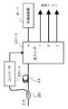
先ず本発明の実施例を図1を用いて説明する。図1は、光バッファ遅延器の一例を示すブロック図である。光路に入力した光信号は、分岐器(あるいはサーキュレータ)3を通り、光遅延素子で、時間的な遅延を受ける、遅延時間は、この光遅延素子の長さできまる。光遅延素子1を通過した光信号は、位相共役鏡2で反射され、光遅延素子1を逆戻りする。光遅延素子1を通過した光信号は、分岐器(あるいはサーキュレータ)3により、出力用の光路に振り向けられる。このように出力される光信号は、光遅延素子1を往復する際に波長分散効果が往路と復路で相殺される。 First, an embodiment of the present invention will be described with reference to FIG. FIG. 1 is a block diagram illustrating an example of an optical buffer delay device. The optical signal input to the optical path passes through the branching unit (or circulator) 3 and is subjected to a time delay by the optical delay element. The delay time is determined by the length of the optical delay element. The optical signal that has passed through the
ここで、位相共役鏡による反射は、通常の反射とは異なり、図2(a)に示すように、位相共役光生成器で生成された位相共役光を入力部と位置を同じくする出力部から出力するものである。位相共役光を生成する方法は、すでにいくつかの方法が報告されており、4光波混合、ブリルアン散乱、フオトリフラクティブ媒質を用いた自己励起型位相共役発生などによる方法で発生することが出来ることが知られている。 Here, the reflection by the phase conjugate mirror is different from the normal reflection. As shown in FIG. 2A, the phase conjugate light generated by the phase conjugate light generator is output from the output unit having the same position as the input unit. Output. Several methods for generating phase conjugate light have already been reported, and can be generated by methods such as four-wave mixing, Brillouin scattering, and self-excited phase conjugation using a photorefractive medium. Are known.
また、通常の位相共役光では、入力した光信号から、僅かに波長シフトを受けている。入力した光信号と同じ波長の光信号を出力することができ場合は、波長分割多重変調方式においても使用することができるので、光通信に用いる場合は、波長シフトが無い位相共役光の方が都合がよい場合がある。このための位相共役鏡は図2(b)に示すブロック図のように、無波長シフト位相共役光生成器を用いる。また、図3(a)に、無波長シフト位相共役光生成器のブロック図の一例を示す。これは、4光波混合によるものである。また、図3(b)に、ポンプ光A16、ポンプ光B19、光信号17、位相共役光(OPC)信号18の直交関係を示す。 In addition, ordinary phase conjugate light undergoes a slight wavelength shift from the input optical signal. If an optical signal with the same wavelength as the input optical signal can be output, it can also be used in the wavelength division multiplexing modulation method. Therefore, when used for optical communication, phase conjugate light without wavelength shift is better. It may be convenient. The phase conjugate mirror for this uses a non-wavelength shifted phase conjugate light generator as shown in the block diagram of FIG. FIG. 3A shows an example of a block diagram of a non-wavelength shifted phase conjugate light generator. This is due to four-wave mixing. FIG. 3B shows an orthogonal relationship among the pump light A16, the pump light B19, the
図3(a)に示す無波長シフト位相共役光生成器では、入力した波長1550.12nmの光信号は、光増幅器7−1(EDFA:エルビウム添加ファイバ増幅器)で増幅された後、帯域幅5nmの濾波器8−1を通り、偏光子9−1として動作する偏波保持ファイバを通り、波長1544.91nmのレーザ光源6−1からのレーザ光と合波器10−1で合波される。一方、レーザ光源6−1からのレーザ光は、光増幅器7−2で増幅された後、帯域幅5nmの濾波器8−2を通り、偏光子9−2を通り、合波器10−1に送られる。ここで、光増幅器としては、半導体型の光増幅器を適用することもできる。また、偏光子としては、偏光板や全反射角を用いたものでも代用することができる。また、レーザ光源としては、ダイオードレーザに限定する必要は無く、使用する波長帯のレーザ光を発生するものであれば用いることができる。また、濾波器としては、ファイバブラッグ格子の他にファブリ・ペロ型共振器なども用いることが出来る。 In the non-wavelength shifted phase conjugate light generator shown in FIG. 3A, an input optical signal having a wavelength of 1550.12 nm is amplified by an optical amplifier 7-1 (EDFA: erbium-doped fiber amplifier) and then has a bandwidth of 5 nm. The laser light from the laser light source 6-1 having a wavelength of 1544.91 nm is multiplexed by the multiplexer 10-1 through the filter 8-1 and the polarization maintaining fiber operating as the polarizer 9-1. . On the other hand, the laser light from the laser light source 6-1 is amplified by the optical amplifier 7-2, passes through the filter 8-2 having a bandwidth of 5 nm, passes through the polarizer 9-2, and passes through the multiplexer 10-1. Sent to. Here, as the optical amplifier, a semiconductor-type optical amplifier can also be applied. Moreover, as a polarizer, what uses a polarizing plate and a total reflection angle can be substituted. Further, the laser light source need not be limited to a diode laser, and any laser light source that generates laser light in a wavelength band to be used can be used. In addition to the fiber Bragg grating, a Fabry-Perot resonator can be used as the filter.
合波器10−1からの光信号は、波長1555.36nmのレーザ光源6−2からの光と合波器10−2で合波される。このように合波された光信号は、500m長の高い光非線形性を持った光ファイバ(HNLF)11において、4波混合による直交偏光2重ポンピング法で混合される。光ファイバ(HNLF)11の分散とゼロ分散波長は、0.044ps/nm/km、1548.5nmである。ここで使用できるHNLFはこの仕様のものに限らず、分散値が小さく、光非線形性が大きいものであれば、長さは短くてもよい。また、この光学特性を満足するものであれば、他の非線形素子を用いても差し支えない。 The optical signal from the multiplexer 10-1 is combined with the light from the laser light source 6-2 having a wavelength of 1555.36 nm by the multiplexer 10-2. The optical signals thus combined are mixed by an orthogonal polarization double pumping method using four-wave mixing in an optical fiber (HNLF) 11 having a high optical nonlinearity of 500 m. The dispersion and zero dispersion wavelength of the optical fiber (HNLF) 11 are 0.044 ps / nm / km and 1548.5 nm. The HNLF that can be used here is not limited to this specification, and the length may be short as long as the dispersion value is small and the optical nonlinearity is large. Also, other nonlinear elements may be used as long as these optical characteristics are satisfied.
ここで、図3(b)に示すように、入力した光信号と、レーザ光源6−1からのポンプ光Aとを同じ偏光方向に設定し、これらと直交する偏光であるレーザ光源6−2からのポンプ光Bとを4光波混合で混合すると、ポンプ光Bと同じ偏光方向をもち、入力した光信号の共役光である光信号が得られる。 Here, as shown in FIG. 3B, the input optical signal and the pump light A from the laser light source 6-1 are set in the same polarization direction, and the laser light source 6-2 is polarized light orthogonal to them. When the pump light B is mixed by four-wave mixing, an optical signal having the same polarization direction as that of the pump light B and being conjugate light of the input optical signal is obtained.
この共役光を偏波フィルタ(ビームスプリッタ)12、濾波器13、光増幅器14、濾波器15により、濾波あるいは増幅することにより、入力した光信号の位相共役光を生成するものである。 The conjugate light is filtered or amplified by the polarization filter (beam splitter) 12, the
図4は、複数の遅延時間を選択できるようにした光バッファ遅延器を示すブロック図である。入力した光信号は、その光信号に設けられたラベルに記載された情報に従って遅延時間が与えられるが、このためには、入力した光信号の一部を分岐して、コントローラ22でその遅延情報を解析する。遅延素子21は、コントローラによる信号遅延と光信号との伝搬遅延との整合をとるためのものである。コントローラ22からの制御信号により、光スイッチ23を制御して、光信号を振り向けるチャネルを決める。例えば、チャネル0では、遅延を与えずに反射する。また、チャネル1から3では、順次遅延時間が増加するように設定する。チャネル1から3では、それぞれの遅延素子を通過した後、それぞれ位相共役鏡により位相共役光が反射される。 FIG. 4 is a block diagram showing an optical buffer delay device in which a plurality of delay times can be selected. The input optical signal is given a delay time according to the information written on the label provided on the optical signal. For this purpose, a part of the input optical signal is branched and the
上記の例では、光遅延素子を用いているが、これを、ネットワークを形成している光ファイバを用いて代用することができる。実際のネットワークを用いることによって、大容量のバッファを作ることができ、既設の伝送路を用いるために、ネットワークの運用率も上がり,コスト低減につながる。図5は、ノードA30、ノードB31、ノードC32が含まれるネットワークを示す。例えば、2つのデータ信号、25−1(光パケットA)と26−1(光パケットB)は、ともにノードCを通過するものとする。データ25−1が、ノードAでデータ26−1と衝突しそうなときには、ノードAは、データ26−1用にノードBへの道を開き、ノードBは、データ26−1用にノードAへの道を開く。つまり光パケットBについては、ノードA−B間を往復させて遅延させる。これでデータ衝突の問題が解消される。In the above example, an optical delay element is used, but this can be substituted by using an optical fiber forming a network. By using an actual network, a large-capacity buffer can be created, and since the existing transmission path is used, the operation rate of the network is increased, leading to cost reduction. FIG. 5 shows a network including node A30, node B31, and node C32. For example, it is assumed that two data signals, 25-1 (optical packet A) and 26-1 (optical packet B), both pass through node C. Data 25-1, when the data 26-1 and the collision was likely in the node A, nodeA, open the way to node B for data 26-1, node B, for data 26-1 to the node A Open the way. That is, the optical packet B is delayed by reciprocating between the nodes A and B. This eliminates the data collision problem.
図5のそれぞれのノードにおいては、位相共役光を反射光として戻す構成をもっており、その構成の一例を図6のブロック図に示す。入力した光信号の一部を分岐器20で分岐して、コントローラ22−1でその光信号に書かれたラベル情報を解析する。このラベル情報が、光信号を反射して戻すことを要求する内容である場合は、コントローラ22−1は、光スイッチ23−1を制御して、光信号を位相共役鏡2−4の接続されたチャネル0に振り向ける。ラベル情報の内容によっては、コントローラ22−1は、光スイッチ23−1を制御して、光信号を他のノードへ続くチャネル1〜3に振り向ける。このような構成にすることにより、複数のノードにまたがる伝送路を遅延用に用いることが可能である。また、上記と同様に、遅延素子21は、コントローラによる信号遅延と光信号との伝搬遅延との整合をとるためのものである。位相共役鏡2−4は、波長シフトのあるものでも波長シフトのないものでも用いることが出来るのは明らかである。 Each node in FIG. 5 has a configuration for returning the phase conjugate light as reflected light, and an example of the configuration is shown in the block diagram of FIG. A part of the input optical signal is branched by the branching
本発明の光バッファ遅延器では、屈折率の大きな材料でつくった光路、あるいは、長さを大きくとった光路などを用いて実現した遅延器で遅延時間を大きく設定しても、原理的に位相分散が発生せず、これによる波形の乱れは発生しない。このため、実際の光バッファ遅延器を用いて光信号遅延を行った場合でも、高速通信においてビット誤り率の増大を抑制することが出来る。従って同じビット誤り率では、より高速で通信できるようになる。 In the optical buffer delay device of the present invention, even if the delay time is set to be large with a delay device realized by using an optical path made of a material having a large refractive index or an optical path having a large length, the phase can be changed in principle. Dispersion does not occur, and waveform disturbance due to this does not occur. For this reason, even when optical signal delay is performed using an actual optical buffer delay device, an increase in bit error rate can be suppressed in high-speed communication. Therefore, communication can be performed at higher speed with the same bit error rate.
1、1−1、1−2、1−3 光遅延素子
2、2−1、2−2、2−3、2−4 位相共役鏡
3 分岐器
4、4−1 分岐器
5 位相共役光生成器
6−1、6−2 レーザ光源
7−1、7−2、7−3 光増幅器
8−1、8−2、8−3 濾波器
9−1、9−2、9−3 偏光子
10−1、10−2 合波器
11 高い非線形性を持った光ファイバ
12 偏波フィルタ
13 濾波器
14 光増幅器
16 ポンプ光A
17 光信号
18 位相共役光信号
19 ポンプ光
20 分岐器
21 遅延器
22、22−1 コントローラ
23、23−1 光スイッチ
24 反射ループ
25、26、27、28、29 光路
25−1、29−1 光パケットA
26−1、27−1、27−2 光パケットBDESCRIPTION OF
DESCRIPTION OF
26-1, 27-1, 27-2 Optical packet B
Claims (3)
Translated fromJapanese伝送された光パケットを複数の光遅延素子から選択した光遅延素子に送る光スイッチと、
上記光スイッチから伝送された光パケットを遅延させる光遅延素子と、
前記光遅延素子からの光の位相共役光を生成する無波長シフト位相共役鏡と、
上記の位相共役光が上記光スイッチから上記無波長シフト位相共役鏡に至る光路を逆にたどる構成と、
上記の光路を逆にたどる前記の位相共役光が上記の光スイッチを通過した後に、上記光通信に用いる新たな光路に前記の位相共役光を振り向ける分岐手段と、を、備えることを特徴とする光バッファ遅延器。An optical buffer delay unit usedfor optical packet switchingin opticalcommunication ,
An optical switchfor sending a transmitted opticalpacket to an optical delay element selected from a plurality of optical delay elements;
An optical delay element which delays the opticalpackets transmitted fromthe optical switch,
A non-wavelength shifted phase conjugate mirror that generates phase conjugate light of light from the optical delay element;
A configuration in which the phase conjugate light traces the optical pathfrom the optical switch to the non-wavelength shifted phase conjugate mirror in reverse;
Branching means for directing the phase conjugate light to anew optical path used for the optical communication after the phase conjugate light tracing the optical path in the reverse direction passes through the optical switch. An optical buffer delay device.
Priority Applications (1)
| Application Number | Priority Date | Filing Date | Title |
|---|---|---|---|
| JP2004218617AJP4431704B2 (en) | 2004-07-27 | 2004-07-27 | Optical buffer delay |
Applications Claiming Priority (1)
| Application Number | Priority Date | Filing Date | Title |
|---|---|---|---|
| JP2004218617AJP4431704B2 (en) | 2004-07-27 | 2004-07-27 | Optical buffer delay |
Publications (2)
| Publication Number | Publication Date |
|---|---|
| JP2006041896A JP2006041896A (en) | 2006-02-09 |
| JP4431704B2true JP4431704B2 (en) | 2010-03-17 |
Family
ID=35906417
Family Applications (1)
| Application Number | Title | Priority Date | Filing Date |
|---|---|---|---|
| JP2004218617AExpired - Fee RelatedJP4431704B2 (en) | 2004-07-27 | 2004-07-27 | Optical buffer delay |
Country Status (1)
| Country | Link |
|---|---|
| JP (1) | JP4431704B2 (en) |
Cited By (6)
| Publication number | Priority date | Publication date | Assignee | Title |
|---|---|---|---|---|
| US7918011B2 (en) | 2000-12-27 | 2011-04-05 | Abbott Cardiovascular Systems, Inc. | Method for providing radiopaque nitinol alloys for medical devices |
| US7938843B2 (en) | 2000-11-02 | 2011-05-10 | Abbott Cardiovascular Systems Inc. | Devices configured from heat shaped, strain hardened nickel-titanium |
| US7942892B2 (en) | 2003-05-01 | 2011-05-17 | Abbott Cardiovascular Systems Inc. | Radiopaque nitinol embolic protection frame |
| US7976648B1 (en) | 2000-11-02 | 2011-07-12 | Abbott Cardiovascular Systems Inc. | Heat treatment for cold worked nitinol to impart a shape setting capability without eventually developing stress-induced martensite |
| WO2015100636A1 (en)* | 2013-12-31 | 2015-07-09 | 华为技术有限公司 | Annular optical buffer and optical signal storage and reading method |
| US9709744B2 (en) | 2013-12-31 | 2017-07-18 | Huawei Technologies Co., Ltd. | Annular optical shifter and method for shifting optical signal |
- 2004
- 2004-07-27JPJP2004218617Apatent/JP4431704B2/ennot_activeExpired - Fee Related
Cited By (6)
| Publication number | Priority date | Publication date | Assignee | Title |
|---|---|---|---|---|
| US7938843B2 (en) | 2000-11-02 | 2011-05-10 | Abbott Cardiovascular Systems Inc. | Devices configured from heat shaped, strain hardened nickel-titanium |
| US7976648B1 (en) | 2000-11-02 | 2011-07-12 | Abbott Cardiovascular Systems Inc. | Heat treatment for cold worked nitinol to impart a shape setting capability without eventually developing stress-induced martensite |
| US7918011B2 (en) | 2000-12-27 | 2011-04-05 | Abbott Cardiovascular Systems, Inc. | Method for providing radiopaque nitinol alloys for medical devices |
| US7942892B2 (en) | 2003-05-01 | 2011-05-17 | Abbott Cardiovascular Systems Inc. | Radiopaque nitinol embolic protection frame |
| WO2015100636A1 (en)* | 2013-12-31 | 2015-07-09 | 华为技术有限公司 | Annular optical buffer and optical signal storage and reading method |
| US9709744B2 (en) | 2013-12-31 | 2017-07-18 | Huawei Technologies Co., Ltd. | Annular optical shifter and method for shifting optical signal |
Also Published As
| Publication number | Publication date |
|---|---|
| JP2006041896A (en) | 2006-02-09 |
Similar Documents
| Publication | Publication Date | Title |
|---|---|---|
| JP3438770B2 (en) | Optical digital playback device | |
| EP0591042B1 (en) | Arrayed-wave guide grating multi/demultiplexer with loop-back optical paths | |
| JP3158706B2 (en) | Light distribution device | |
| JP4252219B2 (en) | Optical node device and system including the device | |
| JP2002506226A (en) | Optical element for dispersion compensation | |
| JP5194847B2 (en) | Optical packet switch device and optical packet switch method | |
| WO2004113998A1 (en) | Optical modulating device | |
| JPH05505888A (en) | optical device | |
| US6396607B1 (en) | Multi-wavelength all-optical regenerators (MARS) | |
| US7706649B2 (en) | Optical processing device and optical processing method | |
| JPH06202169A (en) | Optical switch | |
| JP4431704B2 (en) | Optical buffer delay | |
| US20040136646A1 (en) | All optical decoding systems for decoding optical encoded data symbols across multiple decoding layers | |
| US20040208571A1 (en) | All optical cross routing using decoding systems for optical encoded data symbols | |
| US7130539B2 (en) | All optical decoding systems for optical encoded data symbols | |
| JP4007985B2 (en) | Light switch | |
| Dolejsky et al. | Flexible reconfigurable entanglement-based quantum key distribution network | |
| JP2001523017A (en) | Optical wavelength converter | |
| EP1137204A1 (en) | Multiwavelength light source device employing annular optical delay circuit | |
| JP3293698B2 (en) | Array waveguide diffraction grating type optical multiplexer / demultiplexer with loopback optical path | |
| US7577357B2 (en) | Optical switch | |
| JP3183605B2 (en) | WDM optical soliton transmission system | |
| JP3553857B2 (en) | Wavelength conversion circuit | |
| US11764872B2 (en) | Optical dispersion compensator | |
| JP3566172B2 (en) | Optical packet buffer |
Legal Events
| Date | Code | Title | Description |
|---|---|---|---|
| A621 | Written request for application examination | Free format text:JAPANESE INTERMEDIATE CODE: A621 Effective date:20070614 | |
| A977 | Report on retrieval | Free format text:JAPANESE INTERMEDIATE CODE: A971007 Effective date:20090526 | |
| A131 | Notification of reasons for refusal | Free format text:JAPANESE INTERMEDIATE CODE: A131 Effective date:20090602 | |
| A521 | Written amendment | Free format text:JAPANESE INTERMEDIATE CODE: A523 Effective date:20090714 | |
| A131 | Notification of reasons for refusal | Free format text:JAPANESE INTERMEDIATE CODE: A131 Effective date:20090811 | |
| A521 | Written amendment | Free format text:JAPANESE INTERMEDIATE CODE: A523 Effective date:20091013 | |
| TRDD | Decision of grant or rejection written | ||
| A01 | Written decision to grant a patent or to grant a registration (utility model) | Free format text:JAPANESE INTERMEDIATE CODE: A01 Effective date:20091110 | |
| A01 | Written decision to grant a patent or to grant a registration (utility model) | Free format text:JAPANESE INTERMEDIATE CODE: A01 | |
| A61 | First payment of annual fees (during grant procedure) | Free format text:JAPANESE INTERMEDIATE CODE: A61 Effective date:20091119 | |
| R150 | Certificate of patent or registration of utility model | Free format text:JAPANESE INTERMEDIATE CODE: R150 | |
| FPAY | Renewal fee payment (event date is renewal date of database) | Free format text:PAYMENT UNTIL: 20130108 Year of fee payment:3 | |
| LAPS | Cancellation because of no payment of annual fees |