JP4430918B2 - Thin film forming apparatus cleaning method and thin film forming method - Google Patents
Thin film forming apparatus cleaning method and thin film forming methodDownload PDFInfo
- Publication number
- JP4430918B2 JP4430918B2JP2003371322AJP2003371322AJP4430918B2JP 4430918 B2JP4430918 B2JP 4430918B2JP 2003371322 AJP2003371322 AJP 2003371322AJP 2003371322 AJP2003371322 AJP 2003371322AJP 4430918 B2JP4430918 B2JP 4430918B2
- Authority
- JP
- Japan
- Prior art keywords
- gas
- film forming
- reaction tube
- thin film
- nitrogen
- Prior art date
- Legal status (The legal status is an assumption and is not a legal conclusion. Google has not performed a legal analysis and makes no representation as to the accuracy of the status listed.)
- Expired - Fee Related
Links
- 238000000034methodMethods0.000titleclaimsdescription137
- 239000010409thin filmSubstances0.000titleclaimsdescription77
- 238000004140cleaningMethods0.000titleclaimsdescription69
- 238000006243chemical reactionMethods0.000claimsdescription212
- 239000007789gasSubstances0.000claimsdescription165
- IJGRMHOSHXDMSA-UHFFFAOYSA-NAtomic nitrogenChemical compoundN#NIJGRMHOSHXDMSA-UHFFFAOYSA-N0.000claimsdescription112
- 239000010408filmSubstances0.000claimsdescription98
- 238000010926purgeMethods0.000claimsdescription75
- 239000010453quartzSubstances0.000claimsdescription75
- VYPSYNLAJGMNEJ-UHFFFAOYSA-Nsilicon dioxideInorganic materialsO=[Si]=OVYPSYNLAJGMNEJ-UHFFFAOYSA-N0.000claimsdescription75
- YCKRFDGAMUMZLT-UHFFFAOYSA-NFluorine atomChemical compound[F]YCKRFDGAMUMZLT-UHFFFAOYSA-N0.000claimsdescription72
- 229910052731fluorineInorganic materials0.000claimsdescription72
- 239000011737fluorineSubstances0.000claimsdescription72
- 229910052757nitrogenInorganic materials0.000claimsdescription46
- 238000010438heat treatmentMethods0.000claimsdescription45
- MWUXSHHQAYIFBG-UHFFFAOYSA-NNitric oxideChemical compoundO=[N]MWUXSHHQAYIFBG-UHFFFAOYSA-N0.000claimsdescription19
- 239000000463materialSubstances0.000claimsdescription12
- 150000004767nitridesChemical class0.000claimsdescription12
- 230000003213activating effectEffects0.000claimsdescription4
- QGZKDVFQNNGYKY-UHFFFAOYSA-NAmmoniaChemical compoundNQGZKDVFQNNGYKY-UHFFFAOYSA-N0.000description86
- 235000012431wafersNutrition0.000description62
- 229910052581Si3N4Inorganic materials0.000description46
- 239000004065semiconductorSubstances0.000description46
- HQVNEWCFYHHQES-UHFFFAOYSA-Nsilicon nitrideChemical compoundN12[Si]34N5[Si]62N3[Si]51N64HQVNEWCFYHHQES-UHFFFAOYSA-N0.000description46
- 239000012535impuritySubstances0.000description39
- 238000011109contaminationMethods0.000description31
- 229910052751metalInorganic materials0.000description31
- 239000002184metalSubstances0.000description31
- 229910021529ammoniaInorganic materials0.000description29
- 238000009792diffusion processMethods0.000description29
- 230000015572biosynthetic processEffects0.000description21
- 229910001873dinitrogenInorganic materials0.000description21
- RYGMFSIKBFXOCR-UHFFFAOYSA-NCopperChemical compound[Cu]RYGMFSIKBFXOCR-UHFFFAOYSA-N0.000description10
- 239000010949copperSubstances0.000description10
- 229910052802copperInorganic materials0.000description10
- 239000007795chemical reaction productSubstances0.000description7
- 230000006641stabilisationEffects0.000description7
- 238000011105stabilizationMethods0.000description7
- -1for exampleSubstances0.000description6
- PXHVJJICTQNCMI-UHFFFAOYSA-NNickelChemical compound[Ni]PXHVJJICTQNCMI-UHFFFAOYSA-N0.000description5
- 150000002500ionsChemical group0.000description5
- 238000005121nitridingMethods0.000description5
- 238000011068loading methodMethods0.000description4
- 238000002156mixingMethods0.000description4
- KRHYYFGTRYWZRS-UHFFFAOYSA-NFluoraneChemical compoundFKRHYYFGTRYWZRS-UHFFFAOYSA-N0.000description3
- 230000004913activationEffects0.000description3
- 239000000460chlorineSubstances0.000description3
- 239000011651chromiumSubstances0.000description3
- 239000000356contaminantSubstances0.000description3
- 229910000040hydrogen fluorideInorganic materials0.000description3
- 239000012212insulatorSubstances0.000description3
- 238000005259measurementMethods0.000description3
- 150000002829nitrogenChemical class0.000description3
- 239000002245particleSubstances0.000description3
- VYZAMTAEIAYCRO-UHFFFAOYSA-NChromiumChemical compound[Cr]VYZAMTAEIAYCRO-UHFFFAOYSA-N0.000description2
- GQPLMRYTRLFLPF-UHFFFAOYSA-NNitrous OxideChemical compound[O-][N+]#NGQPLMRYTRLFLPF-UHFFFAOYSA-N0.000description2
- XUIMIQQOPSSXEZ-UHFFFAOYSA-NSiliconChemical compound[Si]XUIMIQQOPSSXEZ-UHFFFAOYSA-N0.000description2
- 238000005229chemical vapour depositionMethods0.000description2
- 229910052804chromiumInorganic materials0.000description2
- 230000006837decompressionEffects0.000description2
- 230000000694effectsEffects0.000description2
- 238000004519manufacturing processMethods0.000description2
- 229910052759nickelInorganic materials0.000description2
- 229960001730nitrous oxideDrugs0.000description2
- 238000007789sealingMethods0.000description2
- 229910052710siliconInorganic materials0.000description2
- 239000010703siliconSubstances0.000description2
- 238000009751slip formingMethods0.000description2
- 238000005979thermal decomposition reactionMethods0.000description2
- DDFHBQSCUXNBSA-UHFFFAOYSA-N5-(5-carboxythiophen-2-yl)thiophene-2-carboxylic acidChemical compoundS1C(C(=O)O)=CC=C1C1=CC=C(C(O)=O)S1DDFHBQSCUXNBSA-UHFFFAOYSA-N0.000description1
- ZAMOUSCENKQFHK-UHFFFAOYSA-NChlorine atomChemical compound[Cl]ZAMOUSCENKQFHK-UHFFFAOYSA-N0.000description1
- CGRVKSPUKAFTBN-UHFFFAOYSA-NN-silylbutan-1-amineChemical compoundCCCCN[SiH3]CGRVKSPUKAFTBN-UHFFFAOYSA-N0.000description1
- 229910017855NH 4 FInorganic materials0.000description1
- ODUCDPQEXGNKDN-UHFFFAOYSA-NNitrogen oxide(NO)Natural productsO=NODUCDPQEXGNKDN-UHFFFAOYSA-N0.000description1
- 229910003902SiCl 4Inorganic materials0.000description1
- BLRPTPMANUNPDV-UHFFFAOYSA-NSilaneChemical compound[SiH4]BLRPTPMANUNPDV-UHFFFAOYSA-N0.000description1
- NRTOMJZYCJJWKI-UHFFFAOYSA-NTitanium nitrideChemical compound[Ti]#NNRTOMJZYCJJWKI-UHFFFAOYSA-N0.000description1
- 239000002253acidSubstances0.000description1
- 239000003054catalystSubstances0.000description1
- 229910052801chlorineInorganic materials0.000description1
- SLLGVCUQYRMELA-UHFFFAOYSA-NchlorosiliconChemical compoundCl[Si]SLLGVCUQYRMELA-UHFFFAOYSA-N0.000description1
- 230000007423decreaseEffects0.000description1
- 238000000151depositionMethods0.000description1
- MROCJMGDEKINLD-UHFFFAOYSA-NdichlorosilaneChemical compoundCl[SiH2]ClMROCJMGDEKINLD-UHFFFAOYSA-N0.000description1
- 238000010790dilutionMethods0.000description1
- 239000012895dilutionSubstances0.000description1
- PZPGRFITIJYNEJ-UHFFFAOYSA-NdisilaneChemical compound[SiH3][SiH3]PZPGRFITIJYNEJ-UHFFFAOYSA-N0.000description1
- 238000001312dry etchingMethods0.000description1
- 239000003344environmental pollutantSubstances0.000description1
- 239000011521glassSubstances0.000description1
- 229910052736halogenInorganic materials0.000description1
- 150000002367halogensChemical class0.000description1
- 239000003779heat-resistant materialSubstances0.000description1
- 235000013842nitrous oxideNutrition0.000description1
- 238000006303photolysis reactionMethods0.000description1
- 230000015843photosynthesis, light reactionEffects0.000description1
- 231100000719pollutantToxicity0.000description1
- 238000001004secondary ion mass spectrometryMethods0.000description1
- FDNAPBUWERUEDA-UHFFFAOYSA-Nsilicon tetrachlorideChemical compoundCl[Si](Cl)(Cl)ClFDNAPBUWERUEDA-UHFFFAOYSA-N0.000description1
- 229910001220stainless steelInorganic materials0.000description1
- 239000010935stainless steelSubstances0.000description1
- 239000000758substrateSubstances0.000description1
- 230000009466transformationEffects0.000description1
- LXEXBJXDGVGRAR-UHFFFAOYSA-Ntrichloro(trichlorosilyl)silaneChemical compoundCl[Si](Cl)(Cl)[Si](Cl)(Cl)ClLXEXBJXDGVGRAR-UHFFFAOYSA-N0.000description1
- ZDHXKXAHOVTTAH-UHFFFAOYSA-NtrichlorosilaneChemical compoundCl[SiH](Cl)ClZDHXKXAHOVTTAH-UHFFFAOYSA-N0.000description1
- 239000005052trichlorosilaneSubstances0.000description1
- 238000011144upstream manufacturingMethods0.000description1
Images


Classifications
- H—ELECTRICITY
- H01—ELECTRIC ELEMENTS
- H01L—SEMICONDUCTOR DEVICES NOT COVERED BY CLASS H10
- H01L21/00—Processes or apparatus adapted for the manufacture or treatment of semiconductor or solid state devices or of parts thereof
- H01L21/02—Manufacture or treatment of semiconductor devices or of parts thereof
- H01L21/04—Manufacture or treatment of semiconductor devices or of parts thereof the devices having potential barriers, e.g. a PN junction, depletion layer or carrier concentration layer
- H01L21/18—Manufacture or treatment of semiconductor devices or of parts thereof the devices having potential barriers, e.g. a PN junction, depletion layer or carrier concentration layer the devices having semiconductor bodies comprising elements of Group IV of the Periodic Table or AIIIBV compounds with or without impurities, e.g. doping materials
- H01L21/30—Treatment of semiconductor bodies using processes or apparatus not provided for in groups H01L21/20 - H01L21/26
- H01L21/31—Treatment of semiconductor bodies using processes or apparatus not provided for in groups H01L21/20 - H01L21/26 to form insulating layers thereon, e.g. for masking or by using photolithographic techniques; After treatment of these layers; Selection of materials for these layers
- C—CHEMISTRY; METALLURGY
- C23—COATING METALLIC MATERIAL; COATING MATERIAL WITH METALLIC MATERIAL; CHEMICAL SURFACE TREATMENT; DIFFUSION TREATMENT OF METALLIC MATERIAL; COATING BY VACUUM EVAPORATION, BY SPUTTERING, BY ION IMPLANTATION OR BY CHEMICAL VAPOUR DEPOSITION, IN GENERAL; INHIBITING CORROSION OF METALLIC MATERIAL OR INCRUSTATION IN GENERAL
- C23C—COATING METALLIC MATERIAL; COATING MATERIAL WITH METALLIC MATERIAL; SURFACE TREATMENT OF METALLIC MATERIAL BY DIFFUSION INTO THE SURFACE, BY CHEMICAL CONVERSION OR SUBSTITUTION; COATING BY VACUUM EVAPORATION, BY SPUTTERING, BY ION IMPLANTATION OR BY CHEMICAL VAPOUR DEPOSITION, IN GENERAL
- C23C16/00—Chemical coating by decomposition of gaseous compounds, without leaving reaction products of surface material in the coating, i.e. chemical vapour deposition [CVD] processes
- C23C16/44—Chemical coating by decomposition of gaseous compounds, without leaving reaction products of surface material in the coating, i.e. chemical vapour deposition [CVD] processes characterised by the method of coating
- C23C16/4401—Means for minimising impurities, e.g. dust, moisture or residual gas, in the reaction chamber
- C23C16/4408—Means for minimising impurities, e.g. dust, moisture or residual gas, in the reaction chamber by purging residual gases from the reaction chamber or gas lines
- C—CHEMISTRY; METALLURGY
- C23—COATING METALLIC MATERIAL; COATING MATERIAL WITH METALLIC MATERIAL; CHEMICAL SURFACE TREATMENT; DIFFUSION TREATMENT OF METALLIC MATERIAL; COATING BY VACUUM EVAPORATION, BY SPUTTERING, BY ION IMPLANTATION OR BY CHEMICAL VAPOUR DEPOSITION, IN GENERAL; INHIBITING CORROSION OF METALLIC MATERIAL OR INCRUSTATION IN GENERAL
- C23C—COATING METALLIC MATERIAL; COATING MATERIAL WITH METALLIC MATERIAL; SURFACE TREATMENT OF METALLIC MATERIAL BY DIFFUSION INTO THE SURFACE, BY CHEMICAL CONVERSION OR SUBSTITUTION; COATING BY VACUUM EVAPORATION, BY SPUTTERING, BY ION IMPLANTATION OR BY CHEMICAL VAPOUR DEPOSITION, IN GENERAL
- C23C16/00—Chemical coating by decomposition of gaseous compounds, without leaving reaction products of surface material in the coating, i.e. chemical vapour deposition [CVD] processes
- C23C16/44—Chemical coating by decomposition of gaseous compounds, without leaving reaction products of surface material in the coating, i.e. chemical vapour deposition [CVD] processes characterised by the method of coating
- C23C16/4401—Means for minimising impurities, e.g. dust, moisture or residual gas, in the reaction chamber
- C23C16/4404—Coatings or surface treatment on the inside of the reaction chamber or on parts thereof
Landscapes
- Chemical & Material Sciences (AREA)
- Engineering & Computer Science (AREA)
- General Chemical & Material Sciences (AREA)
- Chemical Kinetics & Catalysis (AREA)
- Materials Engineering (AREA)
- Mechanical Engineering (AREA)
- Metallurgy (AREA)
- Organic Chemistry (AREA)
- Physics & Mathematics (AREA)
- Condensed Matter Physics & Semiconductors (AREA)
- General Physics & Mathematics (AREA)
- Manufacturing & Machinery (AREA)
- Computer Hardware Design (AREA)
- Microelectronics & Electronic Packaging (AREA)
- Power Engineering (AREA)
- Chemical Vapour Deposition (AREA)
Description
Translated fromJapanese本発明は、薄膜形成装置の洗浄方法及び薄膜形成方法に関し、詳しくは、薄膜への不純物の混入を抑制する薄膜形成装置の洗浄方法及び薄膜形成方法に関する。The present inventionrelates to a cleaning method and a thin film forming method of thethin film forming apparatus, and more particularly to cleaning method and thin film forming method of thethin film forming apparatusthat to suppress the inclusion of impurities into the thin film.
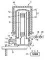
半導体装置の製造工程では、CVD(Chemical Vapor Deposition)等の処理により、被処理体、例えば、半導体ウエハに薄膜を形成する薄膜形成処理が行われている。このような薄膜形成処理では、例えば、図8に示すような熱処理装置51を用い、以下のようにして半導体ウエハに薄膜が形成される。 In the manufacturing process of a semiconductor device, a thin film forming process for forming a thin film on an object to be processed, for example, a semiconductor wafer, is performed by a process such as CVD (Chemical Vapor Deposition). In such a thin film forming process, for example, a
まず、内管52a及び外管52bからなる二重管構造の反応管52内をヒータ53により所定の温度、例えば、760℃に昇温(加熱)する。また、複数枚の半導体ウエハ54を収容したウエハボート55を反応管52(内管52a)内にロードする。次に、排気ポート56から反応管52内のガスを排気し、反応管52内を所定の圧力、例えば、26.5Pa(0.2Torr)に減圧する。反応管52内が所定の圧力に減圧されると、ガス導入管57から内管52a内に処理ガスを供給する。内管52a内に処理ガスが供給されると、処理ガスが熱反応を起こし、熱反応により生成された反応生成物が半導体ウエハ54の表面に堆積して、半導体ウエハ54の表面に薄膜が形成される。 First, the inside of the double-pipe
薄膜形成処理によって発生する排ガスは、排気ポート56に接続された排気管58から熱処理装置51の外部に排気される。なお、排気管58には、図示しないトラップ、スクラバー等が介設されており、トラップ等により排ガスに含まれる反応生成物等を取り除いて無害化した後、熱処理装置51外に排気するように構成されている。 The exhaust gas generated by the thin film forming process is exhausted from the
ところで、薄膜形成処理によって生成される反応生成物は、半導体ウエハ54の表面だけでなく、例えば、内管52aの内壁等の熱処理装置51の内部にも堆積(付着)してしまう。この反応生成物が熱処理装置51内に付着した状態で薄膜形成処理を引き続き行うと、やがて、反応生成物が剥離してパーティクルを発生しやすくなる。そして、このパーティクルが半導体ウエハ54に付着すると、製造される半導体装置の歩留りが低下してしまう。 By the way, the reaction product generated by the thin film forming process is deposited (attached) not only on the surface of the
このため、このような装置では、例えば、パーティクルが発生しない程度の回数だけ薄膜形成処理を行った後、ヒータ53により熱処理装置51内を所定の温度に昇温し、昇温した熱処理装置51内に、例えば、フッ素と含ハロゲン酸性ガスとの混合ガスを供給して、反応管52の内壁等の熱処理装置51内に付着した反応生成物を除去(ドライエッチング)する熱処理装置の洗浄方法が提案されている(例えば、特許文献1)。
しかし、熱処理装置51内にクリーニングガスが供給されると、クリーニングガスに含まれるフッ素が、反応管52内の材料、例えば、石英中に拡散し、熱処理装置51内に窒素ガスを供給してもフッ素が熱処理装置51外に排出されにくい。このように反応管52の石英中にフッ素が拡散された状態で薄膜形成処理を行うと、薄膜形成処理中に反応管52からフッ素が拡散(外方拡散)し、半導体ウエハ54上に形成される薄膜中のフッ素濃度が高くなってしまう。 However, even if the cleaning gas is supplied into the
また、反応管52からのフッ素の外方拡散により、半導体ウエハ54上に形成される薄膜にフッ素系不純物(例えば、SiF)が混入するおそれがある。このように薄膜にフッ素系不純物が混入すると、製造する半導体装置の歩留りが低下してしまう。 Also, fluorine-based impurities (for example, SiF) may be mixed into the thin film formed on the
さらに、このような熱処理装置51では、反応管52内を高温かつ低圧に維持して半導体ウエハ54の表面に反応生成物を堆積させる薄膜形成処理を繰り返し行っているので、装置内部を定期的に洗浄していても、反応管52の材料である石英から微量の不純物が放出(発生)される。例えば、反応管52の材料である石英中には銅等からなる微量の金属汚染物質(金属コンタミ)が含まれており、この金属コンタミが薄膜形成処理中に反応管52から外方拡散する。このような金属コンタミ等の不純物が半導体ウエハ54に付着すると、製造される半導体装置の歩留りが低下してしまう。 Furthermore, in such a
本発明は、上記問題に鑑みてなされたものであり、薄膜への不純物の混入を抑制することができる薄膜形成装置の洗浄方法及び薄膜形成方法を提供することを目的とする。
また、本発明は、薄膜形成中におけるフッ素、金属汚染物質等の不純物の拡散を抑制することができる薄膜形成装置の洗浄方法及び薄膜形成方法を提供することを目的とする。
さらに、本発明は、薄膜中のフッ素、金属汚染物質等の不純物の濃度を低減することができる薄膜形成装置の洗浄方法及び薄膜形成方法を提供することを目的とする。The present invention has been made in view of the above problems, and an object thereof is to provide a cleaning method and a thin film forming method of thethin-film forming apparatusthat can suppress contamination of impurities into the thin film.
The present invention also aims to provide a fluorine, a cleaning method and a thin film forming method of thethin-film forming apparatusthat can suppress the diffusion of the impurities of the metal contaminants such as in the thin film formation.
Furthermore, the present invention aims at providing fluorine in the thin film, a cleaning method and a thin film forming method of thethin-film forming apparatusthat can reduce the concentration of impurities of metallic pollutants.
上記目的を達成するため、この発明の第1の観点にかかる薄膜形成装置の洗浄方法は、
被処理体を収容する反応室内に処理ガスを供給して被処理体に薄膜を形成する薄膜形成装置の洗浄方法であって、
前記反応室内に、窒素を含む活性化可能な窒素系ガスを供給して、前記反応室内をパージするパージ工程を備え、
前記パージ工程では、前記反応室内を600℃〜1050℃に昇温するとともに、133Pa〜53.3kPaに維持し、当該反応室内に前記窒素系ガスを供給して該窒素系ガスを活性化させ、
前記窒素系ガスに、一酸化二窒素、または、酸化窒素を用いる、
ことを特徴とする。In order to achieve the above object, a thin film forming apparatus cleaning method according to the first aspect of the present invention comprises:
A cleaning method of a thin film forming apparatus for forming a thin film on a target object by supplying a processing gas into a reaction chamber containing the target object,
A purge step of purging the reaction chamber by supplying an activatable nitrogen-based gas containing nitrogen into the reaction chamber;
Wherein the purging step, the temperature is raised the reaction chamber 600 ° C. to 1050 ° C., and maintained at 133Pa~53.3KPa, activating the nitride Motokei gas by supplying the nitrogen-based gas to the reactionchamber,
Nitrogen monoxide or nitric oxide is used as the nitrogen-based gas.
It is characterized by that.
この発明の第2の観点にかかる薄膜形成装置の洗浄方法は、
薄膜形成装置の反応室内に処理ガスを供給して被処理体に薄膜を形成した後、装置内部に付着した付着物を除去する薄膜形成装置の洗浄方法であって、
前記反応室内に、フッ素ガスを含むクリーニングガスを供給して前記付着物を除去する付着物除去工程と、
前記反応室内に、窒素を含む活性化可能な窒素系ガスを供給して、前記反応室内をパージするパージ工程と、を備え、
前記パージ工程では、前記反応室内を600℃〜1050℃に昇温するとともに、133Pa〜53.3kPaに維持し、当該反応室内に前記窒素系ガスを供給して該窒素系ガスを活性化させ、
前記窒素系ガスに、一酸化二窒素、または、酸化窒素を用いる、
ことを特徴とする。The thin film forming apparatus cleaning method according to the second aspect of the present invention comprises:
A method of cleaning a thin film forming apparatus for supplying a processing gas into a reaction chamber of a thin film forming apparatus to form a thin film on an object to be processed and then removing deposits attached to the inside of the apparatus,
A deposit removing step of removing a deposit by supplying a cleaning gas containing fluorine gas into the reaction chamber;
A purge step of purging the reaction chamber by supplying an activatable nitrogen-based gas containing nitrogen into the reaction chamber;
Wherein the purging step, the temperature is raised the reaction chamber 600 ° C. to 1050 ° C., and maintained at 133Pa~53.3KPa, activating the nitride Motokei gas by supplying the nitrogen-based gas to the reactionchamber,
Nitrogen monoxide or nitric oxide is used as the nitrogen-based gas.
It is characterized by that.
前記パージ工程では、前記反応室内に前記窒素系ガスのみを供給して該窒素系ガスを活性化させることが好ましい。Prior Symbol purge step, it is preferable to activate the nitride Motokei gas by supplying only the nitrogen-based gas into the reaction chamber.
前記パージ工程では、前記反応室内を2660Pa〜53.3kPaに維持することが好ましい。前記薄膜形成装置は前記反応室に複数の被処理体を収容するバッチ式薄膜形成装置であることが好ましい。In the purge step, it is preferable to maintain the reaction chamber at 2660 Pa to 53.3 kPa. The thin film forming apparatus is preferably a batch type thin film forming apparatus in which a plurality of objects to be processed are accommodated in the reaction chamber.
前記反応室内の材料としては、例えば石英がある。An example of the material in the reaction chamber is quartz.
この発明の第3の観点にかかる薄膜形成方法は、
この発明の第1または第2の観点にかかる薄膜形成装置の洗浄方法により薄膜形成装置を洗浄する洗浄工程と、
被処理体を収容する反応室内を所定の温度に昇温し、所定の温度に昇温した反応室内に処理ガスを供給して被処理体に薄膜を形成する成膜工程と、
を備える、ことを特徴とする。A thin film forming method according to thethird aspect of the present invention is as follows.
A cleaning step of cleaning the thin film forming apparatus by the cleaning method of the thin film forming apparatus according to the firstor second aspect of the present invention;
A film forming step of heating the reaction chamber containing the object to be processed to a predetermined temperature, supplying a processing gas into the reaction chamber heated to the predetermined temperature to form a thin film on the object to be processed;
It is characterized by comprising.
この構成によれば、反応室内の材料から不純物が放出され難くなり、薄膜への不純物の混入を抑制することができる。 According to this configuration, impurities are hardly released from the material in the reaction chamber, and contamination of impurities into the thin film can be suppressed.
本発明によれば、薄膜への不純物の混入を抑制することができる。 According to the present invention, it is possible to suppress contamination of impurities into the thin film.
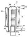
以下、本発明の実施の形態にかかる薄膜形成装置、薄膜形成装置の洗浄方法及び薄膜形成方法について、図1に示すバッチ式縦型熱処理装置1を用いた場合を例に説明する。まず、本実施の形態の熱処理装置1について説明する。 Hereinafter, a thin film forming apparatus, a thin film forming apparatus cleaning method, and a thin film forming method according to an embodiment of the present invention will be described using a case where the batch type vertical heat treatment apparatus 1 shown in FIG. 1 is used as an example. First, the heat treatment apparatus 1 of the present embodiment will be described.
図1に示すように、熱処理装置1は、長手方向が垂直方向に向けられた略円筒状の反応管2を備えている。反応管2は、内管3と、内管3を覆うとともに内管3と一定の間隔を有するように形成された有天井の外管4とから構成された二重管構造を有する。内管3及び外管4は、耐熱材料、例えば、石英により形成されている。 As shown in FIG. 1, the heat treatment apparatus 1 includes a substantially
外管4の下方には、筒状に形成されたステンレス鋼(SUS)からなるマニホールド5が配置されている。マニホールド5は、外管4の下端と気密に接続されている。また、内管3は、マニホールド5の内壁から突出するとともに、マニホールド5と一体に形成された支持リング6に支持されている。 A
マニホールド5の下方には蓋体7が配置され、ボートエレベータ8により蓋体7は上下動可能に構成されている。そして、ボートエレベータ8により蓋体7が上昇すると、マニホールド5の下方側が閉鎖される。 A lid body 7 is disposed below the
蓋体7には、例えば、石英からなるウエハボート9が載置されている。ウエハボート9は、被処理体、例えば、半導体ウエハ10が垂直方向に所定の間隔をおいて複数枚収容可能に構成されている。 A
反応管2の周囲には、反応管2を取り囲むように断熱体11が設けられている。断熱体11の内壁面には、例えば、抵抗発熱体からなる昇温用ヒータ12が設けられている。この昇温用ヒータ12により反応管2の内部が所定の温度に昇温され、この結果、半導体ウエハ10が所定の温度に加熱される。 A
マニホールド5の側面には、処理ガスを導入する処理ガス導入管13が挿通されている。なお、図1では処理ガス導入管13を一つだけ描いている。処理ガス導入管13は、内管3内を臨むように配設されている。例えば、図1に示すように、処理ガス導入管13は、支持リング6より下方(内管3の下方)のマニホールド5の側面に挿通されている。 A processing
処理ガス導入管13は、図示しないマスフローコントローラ等を介して、図示しない所定の処理ガス供給源に接続されている。半導体ウエハ10上にシリコン窒化膜(SiN膜)を形成する場合には、例えば、アンモニア(NH3)ガス供給源、及び、珪素を含むガス供給源に接続されている。珪素を含むガスとしては、例えば、ジクロロシラン(SiH2Cl2:DCS)、ヘキサクロロジシラン(Si2Cl6)、モノシラン(SiH4)、ジシラン(Si2H6)、テトラクロロシラン(SiCl4)、トリクロロシラン(SiHCl3)、ビスターシャルブチルアミノシラン、ヘキサエチルアミノジシランがある。本実施の形態では、DCSガス供給源に接続されている。このため、処理ガス導入管13から所定の流量のアンモニアガス及びDCSガスが内管3内に導入される。The processing
また、マニホールド5の側面には、クリーニングガスを導入するクリーニングガス導入管14が挿通されている。なお、図1ではクリーニングガス導入管14を一つだけ描いている。クリーニングガス導入管14は、内管3内を臨むように配設され、クリーニングガス導入管14からクリーニングガスが内管3内に導入される。また、クリーニングガス導入管14は、図示しないマスフローコントローラ等を介して、図示しない所定のクリーニングガス供給源、例えば、フッ素ガス供給源、フッ化水素ガス供給源及び窒素ガス供給源に接続されている。 A cleaning
また、マニホールド5の側面には、窒素系ガスを導入する窒素系ガス導入管15が挿通されている。窒素系ガスは、窒素を含み、かつ、励起(活性化)可能なガスであればよく、例えば、アンモニア、一酸化二窒素(N2O)、酸化窒素(NO)がある。この窒素系ガスにより、熱処理装置1の内部の材料、例えば、石英を窒化させることが可能になる。Further, a nitrogen-based
窒素系ガス導入管15は内管3内を臨むように配設されている。また、窒素系ガス導入管15は、図示しないマスフローコントローラ等を介して、図示しないガス供給源に接続されている。このため、窒素系ガスは、図示しないガス供給源から窒素系ガス導入管15を介して内管3内に導入される。 The nitrogen-based
マニホールド5の側面には排気口16が設けられている。排気口16は支持リング6より上方に設けられており、反応管2内の内管3と外管4との間に形成された空間に連通する。そして、内管3で発生した排ガス等が内管3と外管4との間の空間を通って排気口16に排気される。また、マニホールド5の側面の排気口16の下方には、パージガスとしての窒素ガスを供給するパージガス供給管17が挿通されている。 An
排気口16には排気管18が気密に接続されている。排気管18には、その上流側から、バルブ19と、真空ポンプ20とが介設されている。バルブ19は、排気管18の開度を調整して、反応管2内の圧力を所定の圧力に制御する。真空ポンプ20は、排気管18を介して反応管2内のガスを排気するとともに、反応管2内の圧力を調整する。 An
なお、排気管18には、図示しないトラップ、スクラバー等が介設されており、反応管2から排気された排ガスを、無害化した後、熱処理装置1外に排気するように構成されている。 The
また、ボートエレベータ8、昇温用ヒータ12、処理ガス導入管13、クリーニングガス導入管14、窒素系ガス導入管15、パージガス供給管17、バルブ19、真空ポンプ20には、制御部21が接続されている。制御部21は、マイクロプロセッサ、プロセスコントローラ等から構成され、熱処理装置1の各部の温度、圧力等を測定し、測定データに基づいて、上記各部に制御信号等を出力し、熱処理装置1の各部を、例えば、図2や図3に示すレシピ(タイムシーケンス)に従って制御する。 A
次に、以上のように構成された熱処理装置1の洗浄方法、及び、この熱処理装置1の洗浄方法を含む薄膜形成方法について説明する。本実施の形態では、反応管2内にアンモニアガス及びDCSガスを導入して半導体ウエハ10上にシリコン窒化膜を形成する場合を例に説明する。また、以下の説明において、熱処理装置1を構成する各部の動作は、制御部21によりコントロールされている。 Next, a cleaning method of the heat treatment apparatus 1 configured as described above and a thin film forming method including the cleaning method of the heat treatment apparatus 1 will be described. In the present embodiment, an example in which ammonia gas and DCS gas are introduced into the
まず、図2のレシピに示すように、熱処理装置1の洗浄方法であるパージ処理と、半導体ウエハ10上にシリコン窒化膜を成膜する成膜処理とを含む薄膜形成方法について説明する。 First, as shown in the recipe of FIG. 2, a thin film forming method including a purge process that is a cleaning method of the heat treatment apparatus 1 and a film forming process for forming a silicon nitride film on the
昇温用ヒータ12により、反応管2内を所定のロード温度、本例では図2(a)に示すように、300℃に昇温し、図2(c)に示すように、パージガス供給管17から反応管2内に所定量の窒素ガスを供給した後、半導体ウエハ10が収容されていないウエハボート9を蓋体7上に載置し、ボートエレベータ8により蓋体7を上昇させ、反応管2を密封する(ロード工程)。 The
次に、反応管2内のガスを排出し、反応管2を所定の圧力に設定する。反応管2の圧力は、133Pa(1.0Torr)〜53.3kPa(400Torr)にすることが好ましい。133Pa(1.0Torr)より低圧であると、後述するアンモニアパージ工程における、反応管2の石英中の不純物(金属コンタミ、フッ素等)の外方拡散や反応管2の石英の窒化が行われにくくなるおそれがあるためである。反応管2の圧力は、2660Pa(20Torr)〜53.3kPa(400Torr)にすることがさらに好ましい。2660Pa(20Torr)以上であると、アンモニアパージ工程における不純物の外方拡散、石英の窒化が促進されるためである。本例では、図2(b)に示すように、2660Pa(20Torr)に設定する。 Next, the gas in the
また、昇温用ヒータ12により、反応管2内を、所定の温度に設定する。反応管2内の温度は、600℃〜1050℃にすることが好ましい。600℃より低温であると、アンモニアパージ工程における、反応管2の石英中の不純物(金属コンタミ、フッ素等)の外方拡散や反応管2の石英の窒化が行われにくくなるおそれがあるためである。一方、1050℃より高温であると、反応管2を形成する石英の軟化点を超えてしまうためである。反応管2内の温度は、800℃〜1050℃にすることがさらに好ましい。800℃以上であると、アンモニアパージ工程における不純物の外方拡散、石英の窒化が促進されるためである。本例では、図2(a)に示すように、900℃に昇温する。そして、この減圧及び昇温操作を、反応管2が所定の圧力及び温度で安定するまで行う(安定化工程)。 Further, the inside of the
反応管2内が所定の圧力及び温度で安定すると、窒素系ガス導入管15から内管3内に、所定量の窒素系ガス、例えば、図2(d)に示すようにアンモニアガスを1リットル/min供給する。所定時間経過後、バルブ19の開度を制御しつつ、真空ポンプ20を駆動させて、反応管2内のガスを排出する。そして、このアンモニアガスの供給及び反応管2内のガスの排出を複数回繰り返す(アンモニアパージ工程)。 When the inside of the
ここで、反応管2等の石英中には、不純物、例えば、金属汚染物質(金属コンタミ)が含まれている。これは、反応管2等を構成する石英中に不純物が混入しないように反応管2を加工するのは困難であり、反応管2等の加工工程の内容やその作業雰囲気等により、銅等の金属が石英中に含まれてしまうためである。内管3内にアンモニアガスが供給されると、反応管2内の熱によりアンモニアが励起(活性化)して反応管2の石英中に含まれる金属コンタミと反応し、金属コンタミが反応管2の石英中から拡散(外方拡散)しやすくなる。このため、反応管2の石英中に含まれる金属コンタミが減少し、成膜処理中における反応管2からの金属コンタミの拡散を抑制することができる。この結果、成膜処理により形成されるシリコン窒化膜中の金属コンタミの量(濃度)を低減することができる。 Here, the quartz of the
また、反応管2等の石英中には、後述するクリーニング処理において拡散されたフッ素が混入(拡散)されている場合がある。内管3内にアンモニアガスが供給されると、活性化されたアンモニアが石英中に拡散されたフッ素と反応し、フッ素が反応管2の石英中から拡散(外方拡散)しやすくなる。このため、反応管2の石英中に拡散されたフッ素が減少し、成膜処理中における反応管2からのフッ素の拡散を抑制することができる。この結果、成膜処理により形成されるシリコン窒化膜中のフッ素の量(濃度)を低減することができる。また、シリコン窒化膜にフッ素系不純物が混入するのを抑制することができる。 In addition, in the quartz of the
さらに、活性化されたアンモニアにより、反応管2等の石英の表面が窒化される。このため、石英中から反応管2内に不純物が外方拡散しにくくなり、後述する成膜工程で形成されるシリコン窒化膜に金属コンタミ等の不純物が混入するのを抑制することができる。特に、活性化されたアンモニアのN*、NH*等のラジカルを利用して、反応管2等の石英の表面を窒化させて窒化膜を形成させると、金属コンタミ等の不純物が石英中から反応管2内に放出されにくくなる。このため、活性化されたアンモニアにより、反応管2等の石英の表面に窒化膜を形成させることがさらに好ましい。Further, the surface of quartz such as the
次に、バルブ19の開度を制御しつつ、真空ポンプ20を駆動させて、反応管2内のガスを排出するとともに、図2(c)に示すように、パージガス供給管17から所定量の窒素ガスを供給して、反応管2内のガスを排気管18に排出する。また、昇温用ヒータ12により、反応管2内を、所定の温度、例えば、図2(a)に示すように、300℃にするとともに、図2(b)に示すように、反応管2内の圧力を常圧に戻す(安定化工程)。そして、ボートエレベータ8により蓋体7を下降させることにより、アンロードする(アンロード工程)。 Next, while controlling the opening degree of the
このように、熱処理装置1を洗浄した後、半導体ウエハ10上にシリコン窒化膜を成膜する成膜処理を行う。 As described above, after the heat treatment apparatus 1 is cleaned, a film forming process for forming a silicon nitride film on the
まず、昇温用ヒータ12により、反応管2内を所定のロード温度、例えば、図2(a)に示すように、300℃とし、ボートエレベータ8により蓋体7が下げられた状態で、半導体ウエハ10が収容されたウエハボート9を蓋体7上に載置する。次に、図2(c)に示すように、パージガス供給管17から反応管2内に所定量の窒素ガスを供給し、ボートエレベータ8により蓋体7を上昇させ、ウエハボート9を反応管2内にロードする。これにより、半導体ウエハ10を反応管2の内管3内に収容するとともに、反応管2を密閉する(ロード工程)。 First, the temperature inside the
反応管2を密閉した後、バルブ19の開度を制御しつつ、真空ポンプ20を駆動させて反応管2内のガスを排出し、反応管2内の減圧を開始する。反応管2内のガスの排出は、反応管2内の圧力を所定の圧力、例えば、図2(b)に示すように、26.5Pa(0.2Torr)になるまで行う。また、昇温用ヒータ12により、反応管2内を所定の温度、例えば、図2(a)に示すように、760℃に昇温する。そして、この減圧及び昇温操作を、反応管2が所定の圧力及び温度で安定するまで行う(安定化工程)。 After sealing the
反応管2内が所定の圧力及び温度で安定すると、パージガス供給管17からの窒素ガスの供給を停止する。そして、処理ガス導入管13から処理ガスとしてのアンモニアガスを所定量、例えば、図2(d)に示すように、0.75リットル/minを内管3内に導入するとともに、処理ガス導入管13から処理ガスとしてのDCSガスを所定量、例えば、図2(e)に示すように、0.075リットル/minを内管3内に導入する。 When the inside of the
アンモニアとDCSガスとが内管3内に導入されると、反応管2内の熱により熱分解反応を起こし、半導体ウエハ10の表面に窒化珪素が堆積される。これにより、半導体ウエハ10の表面にシリコン窒化膜が形成される(成膜工程)。 When ammonia and DCS gas are introduced into the inner tube 3, a thermal decomposition reaction is caused by heat in the
半導体ウエハ10の表面に所定厚のシリコン窒化膜が形成されると、処理ガス導入管13からのアンモニアガス及びDCSガスの供給を停止する。そして、バルブ19の開度を制御しつつ、真空ポンプ20を駆動させて、反応管2内のガスを排出するとともに、図2(c)に示すように、パージガス供給管17から所定量の窒素ガスを供給して、反応管2内のガスを排気管18に排出する(パージ工程)。なお、反応管2内のガスを確実に排出するために、反応管2内のガスの排出及び窒素ガスの供給を複数回繰り返すことが好ましい。 When a silicon nitride film having a predetermined thickness is formed on the surface of the
最後に、図2(c)に示すように、パージガス供給管17から所定量の窒素ガスを供給して、反応管2内を常圧に戻した後、ボートエレベータ8により蓋体7を下降させ、ウエハボート9(半導体ウエハ10)を反応管2からアンロードする(アンロード工程)。 Finally, as shown in FIG. 2 (c), a predetermined amount of nitrogen gas is supplied from the purge
このような成膜処理は、パージ処理を行った後、複数回繰り返し実行することが可能である。例えば、パージ処理を行って熱処理装置1を洗浄した後、所定回数の成膜処理を繰り返すことにより、連続して半導体ウエハ10にシリコン窒化膜を形成することができる。なお、パージ処理と成膜処理とを毎回行うことが好ましい。この場合、形成されるシリコン窒化膜への金属コンタミやフッ素の混入を少なくすることができる。 Such a film formation process can be repeatedly performed a plurality of times after the purge process. For example, the silicon nitride film can be continuously formed on the
以上のような薄膜形成方法により、反応管2の石英中の金属コンタミやフッ素の量を減少させることができ、成膜処理中における反応管2からの金属コンタミ等の拡散を抑制することができる。この結果、成膜処理により形成されるシリコン窒化膜中の不純物の混入を低減することができ、シリコン窒化膜中の不純物の濃度を低減することができる。 By the thin film formation method as described above, the amount of metal contamination and fluorine in the quartz of the
さらに、活性化されたアンモニアのN*、NH*等のラジカルを利用して、反応管2等の石英の表面を窒化させて窒化膜を形成させると、石英中から反応管2内に不純物がさらに拡散(外方拡散)されにくくなる。この結果、成膜処理により形成されるシリコン窒化膜中の不純物の混入を低減することができ、シリコン窒化膜中の不純物の濃度を低減することができる。Further, when a nitride film is formed by nitriding the quartz surface of the
次に、図3のレシピに示すように、成膜処理と、熱処理装置1の内部に付着した窒化珪素を除去するクリーニング処理と、パージ処理とを含む薄膜形成方法について説明する。このクリーニング処理とパージ処理とが、本発明の薄膜形成装置の洗浄方法を構成する。 Next, as shown in the recipe of FIG. 3, a thin film forming method including a film forming process, a cleaning process for removing silicon nitride adhering to the inside of the heat treatment apparatus 1, and a purge process will be described. The cleaning process and the purge process constitute the thin film forming apparatus cleaning method of the present invention.
まず、昇温用ヒータ12により、反応管2内を所定のロード温度、例えば、図3(a)に示すように、300℃に昇温し、ボートエレベータ8により蓋体7が下げられた状態で、半導体ウエハ10が収容されたウエハボート9を蓋体7上に載置する。次に、図3(c)に示すように、パージガス供給管17から反応管2内に所定量の窒素ガスを供給し、ボートエレベータ8により蓋体7を上昇させ、ウエハボート9を反応管2内にロードする。これにより、半導体ウエハ10を反応管2の内管3内に収容するとともに、反応管2を密閉する(ロード工程)。 First, the temperature inside the
反応管2を密閉した後、バルブ19の開度を制御しつつ、真空ポンプ20を駆動させて反応管2内のガスを排出し、反応管2内の減圧を開始する。反応管2内のガスの排出は、反応管2内の圧力を所定の圧力、例えば、図3(b)に示すように、26.5Pa(0.2Torr)になるまで行う。また、昇温用ヒータ12により、反応管2内を所定の温度、例えば、図3(a)に示すように、760℃に昇温する。そして、この減圧及び昇温操作を、反応管2が所定の圧力及び温度で安定するまで行う(安定化工程)。 After sealing the
反応管2内が所定の圧力及び温度で安定すると、パージガス供給管17からの窒素ガスの供給を停止する。そして、処理ガス導入管13から処理ガスとしてのアンモニアガスを所定量、例えば、図3(d)に示すように、0.75リットル/minを内管3内に導入するとともに、処理ガス導入管13から処理ガスとしてのDCSガスを所定量、例えば、図3(e)に示すように、0.075リットル/minを内管3内に導入する。内管3内に導入されたアンモニアとDCSガスとが反応管2内の熱により熱分解反応を起こし、半導体ウエハ10の表面に窒化珪素が堆積される。これにより、半導体ウエハ10の表面にシリコン窒化膜が形成される(成膜工程)。 When the inside of the
半導体ウエハ10の表面に所定厚のシリコン窒化膜が形成されると、処理ガス導入管13からアンモニアガス及びDCSガスの供給を停止する。そして、バルブ19の開度を制御しつつ、真空ポンプ20を駆動させて、反応管2内のガスを排出するとともに、図3(c)に示すように、パージガス供給管17から所定量の窒素ガスを供給して、反応管2内のガスを排気管18に排出する(パージ工程)。 When a silicon nitride film having a predetermined thickness is formed on the surface of the
最後に、図3(c)に示すように、パージガス供給管17から所定量の窒素ガスを供給して、反応管2内を常圧に戻した後、ボートエレベータ8により蓋体7を下降させ、ウエハボート9(半導体ウエハ10)を反応管2からアンロードする(アンロード工程)。 Finally, as shown in FIG. 3C, a predetermined amount of nitrogen gas is supplied from the purge
以上のような成膜処理を複数回行うと、成膜処理によって生成される窒化珪素が、半導体ウエハ10の表面だけでなく、内管3の内壁のような熱処理装置1の内部にも堆積(付着)する。このため、成膜処理を所定回数行った後、熱処理装置1の内部に付着した窒化珪素を除去するクリーニング処理を行う。クリーニング処理では、フッ素ガス(F2)を含むクリーニングガス、例えば、フッ素ガスと、フッ化水素ガス(HF)と、希釈ガスとしての窒素ガス(N2)とからなるガスを、熱処理装置1(反応管2)内に供給する。以下、熱処理装置1のクリーニング処理について説明する。When the film forming process as described above is performed a plurality of times, silicon nitride generated by the film forming process is deposited not only on the surface of the
まず、図3(c)に示すように、パージガス供給管17から反応管2内に所定量の窒素ガスを供給した後、半導体ウエハ10が収容されていないウエハボート9を蓋体7上に載置し、ボートエレベータ8により蓋体7を上昇させ、反応管2を密封する(ロード工程)。 First, as shown in FIG. 3C, after supplying a predetermined amount of nitrogen gas from the purge
次に、反応管2内のガスを排出し、反応管2を所定の圧力、例えば、図3(b)に示すように、20000Pa(150Torr)に維持する。また、昇温用ヒータ12により、反応管2内を、所定の温度、例えば、図3(a)に示すように、300℃に昇温(維持)する。そして、この減圧及び昇温操作を、反応管2が所定の圧力及び温度で安定するまで行う(安定化工程)。 Next, the gas in the
反応管2内が所定の圧力及び温度で安定すると、クリーニングガス導入管14から、所定量のクリーニングガス、例えば、図3(f)に示すようにフッ素ガス2リットル/min、図3(g)に示すようにフッ化水素ガス2リットル/min、及び、図3(c)に示すように、窒素ガス8リットル/minを内管3内に導入する。導入されたクリーニングガスは内管3内で加熱され、内管3内から、内管3と外管4との間に形成された空間を介して排気管18に排出されることにより、内管3の内壁及び外壁、外管4の内壁、排気管18の内壁、ボート9等の熱処理装置1の内部に付着した窒化珪素に接触し、窒化珪素がエッチングされる。これにより、熱処理装置1の内部に付着した窒化珪素が除去される(クリーニング工程)。 When the inside of the
ここで、クリーニング工程により反応管2内にフッ素ガスが供給されると、反応管2内の材料、例えば、反応管2を構成する石英中にフッ素が拡散してしまう。反応管2の石英中にフッ素が拡散された状態で成膜処理を行うと、成膜処理中に反応管2からフッ素が拡散(外方拡散)し、例えば、半導体ウエハ10上に形成されたシリコン窒化膜中のフッ素濃度が高くなってしまう。さらに、反応管2からのフッ素の外方拡散により、半導体ウエハ10上に形成される薄膜にフッ素系不純物(例えば、SiF)が混入するおそれがある。このため、クリーニング処理を行った後、熱処理装置1の内部をパージするパージ処理を行う。パージ処理では、反応管2内のクリーニングガスを排気するとともに、成膜処理中に反応管2からのフッ素の拡散を抑制する。以下、パージ処理について説明する。 Here, when fluorine gas is supplied into the
まず、クリーニングガス導入管14からのクリーニングガスの供給を停止する。次に、パージガス供給管17から反応管2内に所定量の窒素ガスを供給して反応管2内のガスを排出し、反応管2を所定の圧力、例えば、前述の133Pa(1.0Torr)〜53.3kPa(400Torr)に設定する。本例では、図3(b)に示すように、2660Pa(20Torr)に設定する。また、昇温用ヒータ12により、反応管2内を所定の温度、例えば、前述の600℃〜1050℃に設定する。本例では、図3(a)に示すように、900℃に昇温する。そして、この減圧及び昇温操作を、反応管2が所定の圧力及び温度で安定するまで行う(安定化工程)。 First, the supply of the cleaning gas from the cleaning
反応管2内が所定の圧力及び温度で安定すると、窒素系ガス導入管15から内管3内に、所定量の窒素系ガス、例えば、図3(d)に示すようにアンモニアガスを1リットル/min供給する。所定時間経過後、バルブ19の開度を制御しつつ、真空ポンプ20を駆動させて、反応管2内のガスを排出する。そして、このアンモニアガスの供給及び反応管2内のガスの排出を複数回繰り返す(アンモニアパージ工程)。 When the inside of the
内管3内にアンモニアガスが供給されると、反応管2内の熱によりアンモニアが励起(活性化)する。アンモニアが活性化されると、反応管2の石英中に拡散されたフッ素と反応しやすくなり、例えば、フッ化アンモニウム(NH4F)を生成し、フッ素が反応管2外に排出される。このため、反応管2の石英中に拡散されたフッ素量が減少し、成膜処理中における反応管2からのフッ素の拡散を抑制することができる。この結果、成膜処理により形成されるシリコン窒化膜中のフッ素濃度を低減することができる。また、シリコン窒化膜にSiFのようなフッ素系不純物が混入するのを抑制することができる。When ammonia gas is supplied into the inner tube 3, ammonia is excited (activated) by the heat in the
また、活性化されたアンモニアと反応管2の石英中に含まれる金属コンタミとが反応し、金属コンタミが反応管2の石英中から拡散(外方拡散)しやすくなる。このため、反応管2の石英中に含まれる金属コンタミが減少し、成膜処理中における反応管2からの金属コンタミの拡散を抑制することができる。この結果、成膜処理により形成されるシリコン窒化膜中の金属コンタミの量(濃度)を低減することができる。 In addition, the activated ammonia reacts with metal contamination contained in the quartz of the
さらに、活性化されたアンモニアにより、反応管2の石英の表面が窒化される。このため、石英中のフッ素が反応管2から拡散しにくくなり、成膜処理中における反応管2からのフッ素の拡散を抑制することができる。この結果、成膜処理により形成されるシリコン窒化膜中のフッ素濃度を低減することができる。また、シリコン窒化膜に不純物が混入することを抑制できる。特に、活性化されたアンモニアのN*、NH*等のラジカルを利用して、反応管2等の石英の表面を窒化させて窒化膜を形成させると、石英中から反応管2内に不純物が発生しにくくなる。このため、活性化されたアンモニアにより、反応管2等の石英の表面に窒化膜を形成させることがさらに好ましい。Further, the quartz surface of the
次に、バルブ19の開度を制御しつつ、真空ポンプ20を駆動させて、反応管2内のガスを排出するとともに、パージガス供給管17から所定量の窒素ガスを供給して、反応管2内のガスを排気管18に排出する。また、昇温用ヒータ12により、反応管2内を、所定の温度、例えば、図3(a)に示すように、300℃にするとともに、図3(b)に示すように、反応管2内の圧力を常圧に戻す(安定化工程)。そして、ボートエレベータ8により蓋体7を下降させることにより、アンロードする(アンロード工程)。そして、半導体ウエハ10が収容されたウエハボート9を蓋体7上に載置することにより、半導体ウエハ10上にシリコン窒化膜を形成する成膜処理を行うことが可能になる。 Next, while controlling the opening degree of the
このように、所定回数の成膜処理の後、クリーニング処理及びパージ処理を行う薄膜形成方法を繰り返すことにより、連続して半導体ウエハ10にシリコン窒化膜を形成することができる。なお、成膜処理に続いてクリーニング処理及びパージ処理を毎回行ってもよい。この場合、炉内(反応管2内)が毎回清浄化され、形成されるシリコン窒化膜への金属コンタミやフッ素の混入を少なくすることができる。 As described above, the silicon nitride film can be continuously formed on the
以上のような薄膜形成方法により、クリーニング処理によって反応管2の石英中に拡散したフッ素の量を減少させることができ、成膜処理中における反応管2からのフッ素等の拡散を抑制することができる。このため、成膜処理により形成されるシリコン窒化膜中のフッ素濃度を低減することができる。また、シリコン窒化膜にSiFのようなフッ素系不純物が混入するのを抑制することができる。この結果、成膜処理により形成されるシリコン窒化膜中の不純物の混入を低減することができ、シリコン窒化膜中の不純物の濃度を低減することができる。 By the thin film forming method as described above, the amount of fluorine diffused into the quartz of the
さらに、活性化されたアンモニアのN*、NH*等のラジカルを利用して、反応管2等の石英の表面を窒化させて窒化膜を形成させると、石英中から反応管2内に不純物がさらに拡散(外方拡散)されにくくなる。この結果、成膜処理により形成されるシリコン窒化膜中の不純物の混入を低減することができ、シリコン窒化膜中の不純物の濃度を低減することができる。Further, when a nitride film is formed by nitriding the quartz surface of the
次に、本実施の形態の効果を確認するため、石英チップを熱処理装置1(反応管2)内に収容し、フッ素ガスを含むクリーニングガスを用いてクリーニング処理を行った後、従来の窒素ガスを用いた窒素パージ(N2パージ)を行った場合と、本発明のアンモニアガスを用いたアンモニアパージ(NH3パージ)を行った場合とについて、石英チップの深さ方向におけるフッ素濃度を測定した。また、窒素の二次イオン強度を二次イオン質量分析法(SIMS)により測定した。Next, in order to confirm the effect of the present embodiment, the quartz chip is accommodated in the heat treatment apparatus 1 (reaction tube 2), cleaned using a cleaning gas containing fluorine gas, and then subjected to conventional nitrogen gas. The fluorine concentration in the depth direction of the quartz chip was measured when a nitrogen purge using N2 (N2 purge) was performed and when an ammonia purge using the ammonia gas of the present invention (NH3 purge) was performed. . Further, the secondary ion intensity of nitrogen was measured by secondary ion mass spectrometry (SIMS).
なお、クリーニング処理及びアンモニアパージは、前述の本実施の形態と同一の条件で行った。また、窒素パージは、パージガスに窒素ガスを用いた以外はアンモニアパージと同一の条件で行った。図4に石英チップの深さとフッ素濃度との関係を示し、図5に石英チップの深さと二次イオン強度との関係を示す。 The cleaning process and the ammonia purge were performed under the same conditions as those in the present embodiment described above. The nitrogen purge was performed under the same conditions as the ammonia purge except that nitrogen gas was used as the purge gas. FIG. 4 shows the relationship between the depth of the quartz chip and the fluorine concentration, and FIG. 5 shows the relationship between the depth of the quartz chip and the secondary ion intensity.
図4に示すように、アンモニアパージを行うことにより、石英チップ中に拡散されたフッ素量が減少(抑制)することが確認できた。特に、石英チップ表面では、石英チップ中に拡散されたフッ素量が大きく減少(抑制)することが確認できた。これは、活性化されたアンモニアが石英チップ表面に拡散したフッ素と反応し、フッ素が石英チップ中から排出されたためと考えられる。このため、成膜処理中に石英チップからフッ素が排出されにくくなり、成膜処理におけるフッ素の拡散を抑制することができる。 As shown in FIG. 4, it was confirmed that the amount of fluorine diffused into the quartz chip was reduced (suppressed) by performing the ammonia purge. In particular, on the quartz chip surface, it was confirmed that the amount of fluorine diffused in the quartz chip was greatly reduced (suppressed). This is presumably because the activated ammonia reacted with the fluorine diffused on the quartz chip surface, and the fluorine was discharged from the quartz chip. For this reason, it is difficult for fluorine to be discharged from the quartz chip during the film forming process, and diffusion of fluorine in the film forming process can be suppressed.
また、図5に示すように、アンモニアパージを行うことにより、窒素の二次イオン強度が向上することが確認できた。特に、石英チップ表面では、窒素の二次イオン強度が大きく向上することが確認できた。このように、アンモニアパージにより、石英チップ表面が窒化される。この結果、石英チップからフッ素が排出されにくくなり、成膜処理中におけるフッ素の拡散を抑制することができる。 Further, as shown in FIG. 5, it was confirmed that the secondary ion intensity of nitrogen was improved by performing the ammonia purge. In particular, it was confirmed that the secondary ion intensity of nitrogen was greatly improved on the quartz chip surface. Thus, the quartz chip surface is nitrided by the ammonia purge. As a result, it is difficult for fluorine to be discharged from the quartz chip, and diffusion of fluorine during the film forming process can be suppressed.
続いて、本実施の形態の効果を確認するため、成膜処理及びクリーニング処理を行った後、従来の窒素ガスを用いた窒素パージ(N2パージ)、または、本発明のアンモニアガスを用いたアンモニアパージ(NH3パージ)を行った反応管2内にウエハを入れ、反応管2内を800℃に昇温することによりウエハを加熱した後、加熱されたウエハを取り出して、このウエハ表面上の銅濃度を測定した。この結果を図6に示す。なお、図6に示すように、銅濃度の測定はウエハ面内の所定の5ポイントについて全反射蛍光X線法により行った。また、アンモニアパージ工程における反応管2内の温度を950℃、圧力を15960Pa(120Torr)とし、この温度及び圧力下で、反応管2内にアンモニアガスを2リットル/min供給した。Subsequently, in order to confirm the effect of the present embodiment, after performing the film forming process and the cleaning process, the conventional nitrogen purge using nitrogen gas (N2 purge) or the ammonia gas of the present invention was used. put the wafer into ammonia purge (NH3 purge) the
図6に示すように、アンモニアパージを行うことにより、ウエハ上の銅濃度が1/10に減少することが確認できた。これは、活性化されたアンモニアが石英(反応管2、ウエハボート9等)中に存在した銅と反応し、銅が石英から排出されたためと考えられる。このため、成膜処理中に石英から銅が排出されにくくなり、成膜処理における銅の拡散を抑制することができる。また、クロム(Cr)、ニッケル(Ni)についても同様の濃度測定を行ったところ、アンモニアパージを行うことにより、形成されたシリコン窒化膜中のクロム、ニッケル濃度が減少することが確認できた。 As shown in FIG. 6, it was confirmed that the copper concentration on the wafer was reduced to 1/10 by performing the ammonia purge. This is presumably because the activated ammonia reacted with the copper present in the quartz (
以上説明したように、本実施の形態によれば、アンモニアパージにより反応管2内のフッ素及び金属コンタミの量が減少するので、成膜処理中における反応管2からのフッ素及び金属コンタミの拡散を抑制することができる。この結果、成膜処理により形成されるシリコン窒化膜中のフッ素濃度を低減することができる。また、シリコン窒化膜に金属コンタミ等の不純物が混入することを抑制できる。 As described above, according to the present embodiment, the amount of fluorine and metal contamination in the
また、本実施の形態によれば、アンモニアパージにより反応管2の石英の表面が窒化されるので、成膜処理中における反応管2からのフッ素及び金属コンタミの拡散を抑制することができる。この結果、成膜処理により形成されるシリコン窒化膜中のフッ素濃度を低減することができる。また、シリコン窒化膜に金属コンタミ等の不純物が混入することを抑制できる。 In addition, according to the present embodiment, the quartz surface of the
なお、本発明は、上記の実施の形態に限られず、種々の変形、応用が可能である。以下、本発明に適用可能な他の実施の形態について説明する。 In addition, this invention is not restricted to said embodiment, A various deformation | transformation and application are possible. Hereinafter, other embodiments applicable to the present invention will be described.
上記実施の形態では、活性化されていない窒素系ガスを所定の温度(900℃)に昇温した反応管2内に供給して活性化させる場合を例に本発明を説明したが、例えば、図7に示すように、窒素系ガス導入管15に活性化手段31を設け、活性化された窒素系ガスを反応管2内に供給してもよい。この場合、アンモニアパージ工程における反応管2内の温度を、例えば、600℃以下にしても、石英中の不純物の外方拡散や石英の窒化が行われにくくなるおそれがなくなり、アンモニアパージ工程の低温化を図ることができる。活性化手段31としては、加熱手段、プラズマ発生手段、光分解手段、触媒活性化手段等がある。 In the above embodiment, the present invention has been described by taking as an example the case where an activated nitrogen-based gas is supplied into the
上記実施の形態では、窒素系ガスにアンモニアを用いた場合を例に本発明を説明したが、窒素系ガスは、窒素を含み、かつ、活性化可能なガスであればよく、例えば、一酸化二窒素、酸化窒素であってもよい。また、クリーニングガスは、フッ素を含むものであればよく、例えば、ClF3のように、フッ素と塩素とを含むガスから構成されていてもよい。In the above embodiment, the present invention has been described by taking the case where ammonia is used as the nitrogen-based gas. However, the nitrogen-based gas may be any gas that contains nitrogen and can be activated. It may be dinitrogen or nitric oxide. The cleaning gas only needs to contain fluorine, and may be composed of a gas containing fluorine and chlorine, such as ClF3 .
上記実施の形態では、反応管2等が石英により形成され、この石英中にフッ素等が拡散した場合を例に本発明を説明したが、反応管2等が形成される材料は石英に限定されるものではなく、例えば、SiC材料のように、フッ素が拡散する材料であればよい。ただし、反応管2等には耐熱性が求められるため、耐熱性に優れた材料であることが好ましい。 In the above embodiment, the present invention has been described by taking the case where the
上記実施の形態では、半導体ウエハ10上にシリコン窒化膜を形成する場合を例に本発明を説明したが、成膜処理により熱処理装置1の内部に付着した付着物をフッ素を含むクリーニングガスにより除去するものであればよく、例えば、半導体ウエハ10上に窒化チタン膜を形成する薄膜形成装置であってもよい。 In the above embodiment, the present invention has been described by taking the case of forming a silicon nitride film on the
本実施の形態では、反応管2内の温度を900度、圧力を2660Pa(20Torr)に設定して、アンモニアパージを行った場合を例に本発明を説明したが、反応管2内の温度及び圧力は、これに限定されるものではない。例えば、前述の石英チップ中の銅濃度の測定でのアンモニアパージ条件である、反応管2内の温度を950℃、圧力を15960Pa(120Torr)としてもよい。このように、反応管2内をさらに高温、高圧にすると、反応管2の石英の表面がさらに窒化され、成膜処理中における反応管2からのフッ素等の拡散をさらに抑制することができる。また、クリーニングの頻度は、数回の成膜処理毎に行ってもよいが、例えば、1回の成膜処理毎に行ってもよい。 In the present embodiment, the present invention has been described by taking as an example the case where ammonia purge is performed by setting the temperature in the
本実施の形態では、バッチ式熱処理装置について、反応管2が内管3と外管4とから構成された二重管構造のバッチ式縦型熱処理装置の場合を例に本発明を説明したが、本発明はこれに限定されるものではなく、例えば、内管3を有しない単管構造のバッチ式熱処理装置に適用することも可能である。また、被処理体は半導体ウエハ10に限定されるものではなく、例えば、LCD用のガラス基板等にも適用することができる。 In the present embodiment, the present invention has been described with respect to the batch type heat treatment apparatus, taking as an example the case of a batch type vertical heat treatment apparatus having a double tube structure in which the
1 熱処理装置
2 反応管
3 内管
4 外管
5 マニホールド
6 支持リング
7 蓋体
8 ボートエレベータ
9 ウエハボート
10 半導体ウエハ
11 断熱体
12 昇温用ヒータ
13 処理ガス導入管
14 クリーニングガス導入管
15 窒素系ガス導入管
16 排気口
17 パージガス供給管
18 排気管
19 バルブ
20 真空ポンプ
21 制御部DESCRIPTION OF SYMBOLS 1
Claims (7)
Translated fromJapanese前記反応室内に、窒素を含む活性化可能な窒素系ガスを供給して、前記反応室内をパージするパージ工程を備え、
前記パージ工程では、前記反応室内を600℃〜1050℃に昇温するとともに、133Pa〜53.3kPaに維持し、当該反応室内に前記窒素系ガスを供給して該窒素系ガスを活性化させ、
前記窒素系ガスに、一酸化二窒素、または、酸化窒素を用いる、
ことを特徴とする薄膜形成装置の洗浄方法。A cleaning method of a thin film forming apparatus for forming a thin film on a target object by supplying a processing gas into a reaction chamber containing the target object,
A purge step of purging the reaction chamber by supplying an activatable nitrogen-based gas containing nitrogen into the reaction chamber;
Wherein the purging step, the temperature is raised the reaction chamber 600 ° C. to 1050 ° C., and maintained at 133Pa~53.3KPa, activating the nitride Motokei gas by supplying the nitrogen-based gas to the reactionchamber,
Nitrogen monoxide or nitric oxide is used as the nitrogen-based gas.
A method for cleaning a thin film forming apparatus.
前記反応室内に、フッ素ガスを含むクリーニングガスを供給して前記付着物を除去する付着物除去工程と、
前記反応室内に、窒素を含む活性化可能な窒素系ガスを供給して、前記反応室内をパージするパージ工程と、を備え、
前記パージ工程では、前記反応室内を600℃〜1050℃に昇温するとともに、133Pa〜53.3kPaに維持し、当該反応室内に前記窒素系ガスを供給して該窒素系ガスを活性化させ、
前記窒素系ガスに、一酸化二窒素、または、酸化窒素を用いる、
ことを特徴とする薄膜形成装置の洗浄方法。A method of cleaning a thin film forming apparatus for supplying a processing gas into a reaction chamber of a thin film forming apparatus to form a thin film on an object to be processed and then removing deposits attached to the inside of the apparatus,
A deposit removing step of removing a deposit by supplying a cleaning gas containing fluorine gas into the reaction chamber;
A purge step of purging the reaction chamber by supplying an activatable nitrogen-based gas containing nitrogen into the reaction chamber;
Wherein the purging step, the temperature is raised the reaction chamber 600 ° C. to 1050 ° C., and maintained at 133Pa~53.3KPa, activating the nitride Motokei gas by supplying the nitrogen-based gas to the reactionchamber,
Nitrogen monoxide or nitric oxide is used as the nitrogen-based gas.
A method for cleaning a thin film forming apparatus.
被処理体を収容する反応室内を所定の温度に昇温し、所定の温度に昇温した反応室内に処理ガスを供給して被処理体に薄膜を形成する成膜工程と、
を備える、ことを特徴とする薄膜形成方法。A cleaning step of cleaning the thin film forming apparatus by the cleaning method of the thin film forming apparatus according to any one of claims 1 to6 ;
A film forming step of heating the reaction chamber containing the object to be processed to a predetermined temperature, supplying a processing gas into the reaction chamber heated to the predetermined temperature to form a thin film on the object to be processed;
A thin film forming method characterized by comprising:
Priority Applications (5)
| Application Number | Priority Date | Filing Date | Title |
|---|---|---|---|
| JP2003371322AJP4430918B2 (en) | 2003-03-25 | 2003-10-30 | Thin film forming apparatus cleaning method and thin film forming method |
| TW093107967ATW200501241A (en) | 2003-03-25 | 2004-03-24 | Method for cleaning thin-film forming apparatus |
| KR1020047018897AKR100779823B1 (en) | 2003-03-25 | 2004-03-25 | Thin-film forming apparatus, thin-film forming method and method for cleaning thin-film forming apparatus |
| PCT/JP2004/004205WO2004086482A1 (en) | 2003-03-25 | 2004-03-25 | Method for cleaning thin-film forming apparatus |
| US10/549,851US20060213539A1 (en) | 2003-03-25 | 2004-03-25 | Method for cleaning thin-film forming apparatus |
Applications Claiming Priority (2)
| Application Number | Priority Date | Filing Date | Title |
|---|---|---|---|
| JP2003083527 | 2003-03-25 | ||
| JP2003371322AJP4430918B2 (en) | 2003-03-25 | 2003-10-30 | Thin film forming apparatus cleaning method and thin film forming method |
Related Child Applications (1)
| Application Number | Title | Priority Date | Filing Date |
|---|---|---|---|
| JP2009266448ADivisionJP5197554B2 (en) | 2003-03-25 | 2009-11-24 | Thin film forming apparatus cleaning method and thin film forming method |
Publications (2)
| Publication Number | Publication Date |
|---|---|
| JP2004311929A JP2004311929A (en) | 2004-11-04 |
| JP4430918B2true JP4430918B2 (en) | 2010-03-10 |
Family
ID=33100377
Family Applications (1)
| Application Number | Title | Priority Date | Filing Date |
|---|---|---|---|
| JP2003371322AExpired - Fee RelatedJP4430918B2 (en) | 2003-03-25 | 2003-10-30 | Thin film forming apparatus cleaning method and thin film forming method |
Country Status (5)
| Country | Link |
|---|---|
| US (1) | US20060213539A1 (en) |
| JP (1) | JP4430918B2 (en) |
| KR (1) | KR100779823B1 (en) |
| TW (1) | TW200501241A (en) |
| WO (1) | WO2004086482A1 (en) |
Families Citing this family (30)
| Publication number | Priority date | Publication date | Assignee | Title |
|---|---|---|---|---|
| JP4272486B2 (en)* | 2003-08-29 | 2009-06-03 | 東京エレクトロン株式会社 | Thin film forming apparatus and thin film forming apparatus cleaning method |
| JP4541864B2 (en) | 2004-12-14 | 2010-09-08 | 東京エレクトロン株式会社 | Method, apparatus and program for forming silicon oxynitride film |
| TWI365919B (en)* | 2004-12-28 | 2012-06-11 | Tokyo Electron Ltd | Film formation apparatus and method of using the same |
| US7691208B2 (en) | 2005-08-31 | 2010-04-06 | Tokyo Electron Limited | Cleaning method |
| JP4844261B2 (en)* | 2006-06-29 | 2011-12-28 | 東京エレクトロン株式会社 | Film forming method, film forming apparatus, and storage medium |
| JP4245012B2 (en)* | 2006-07-13 | 2009-03-25 | 東京エレクトロン株式会社 | Processing apparatus and cleaning method thereof |
| JP4990594B2 (en)* | 2006-10-12 | 2012-08-01 | 東京エレクトロン株式会社 | Gas supply apparatus, gas supply method, thin film forming apparatus cleaning method, thin film forming method, and thin film forming apparatus |
| JP5008957B2 (en)* | 2006-11-30 | 2012-08-22 | 東京エレクトロン株式会社 | Silicon nitride film forming method, forming apparatus, forming apparatus processing method, and program |
| US20080142046A1 (en)* | 2006-12-13 | 2008-06-19 | Andrew David Johnson | Thermal F2 etch process for cleaning CVD chambers |
| US8080109B2 (en)* | 2007-05-14 | 2011-12-20 | Tokyo Electron Limited | Film formation apparatus and method for using the same |
| JP2008283148A (en)* | 2007-05-14 | 2008-11-20 | Tokyo Electron Ltd | Cleaning method for thin film forming apparatus, thin film forming method, and thin film forming apparatus |
| JP5554469B2 (en)* | 2007-05-14 | 2014-07-23 | 東京エレクトロン株式会社 | Thin film forming apparatus cleaning method, thin film forming method, and thin film forming apparatus |
| US20100186774A1 (en)* | 2007-09-19 | 2010-07-29 | Hironobu Miya | Cleaning method and substrate processing apparatus |
| JP4918453B2 (en)* | 2007-10-11 | 2012-04-18 | 東京エレクトロン株式会社 | Gas supply apparatus and thin film forming apparatus |
| JP5113705B2 (en)* | 2007-10-16 | 2013-01-09 | 東京エレクトロン株式会社 | Thin film forming apparatus cleaning method, thin film forming method, thin film forming apparatus, and program |
| JP4531833B2 (en)* | 2007-12-05 | 2010-08-25 | 株式会社日立国際電気 | Substrate processing apparatus, semiconductor device manufacturing method, and cleaning method |
| JP5044579B2 (en)* | 2009-01-27 | 2012-10-10 | 東京エレクトロン株式会社 | Thin film forming apparatus cleaning method, thin film forming method, thin film forming apparatus, and program |
| US20110000508A1 (en)* | 2009-07-02 | 2011-01-06 | L'Air Liquide, Societe Anonyme pour I'Etude et l'Exploitation des Procedes Georges Claude | Method of removing residual fluorine from deposition chamber |
| US20110117728A1 (en)* | 2009-08-27 | 2011-05-19 | Applied Materials, Inc. | Method of decontamination of process chamber after in-situ chamber clean |
| JP5571233B2 (en)* | 2013-06-19 | 2014-08-13 | 東京エレクトロン株式会社 | Thin film forming apparatus cleaning method, thin film forming method, and thin film forming apparatus |
| KR101516587B1 (en)* | 2014-01-27 | 2015-05-04 | 주식회사 엘지실트론 | Method for cleaning wafer anneal furnace |
| JP2015192063A (en)* | 2014-03-28 | 2015-11-02 | 東京エレクトロン株式会社 | Cleaning method of amorphous silicon film formation device, formation method of amorphous silicon film and amorphous silicon film formation device |
| CN109844904B (en) | 2016-08-05 | 2023-04-28 | 应用材料公司 | Aluminum fluoride reduction by plasma treatment |
| CN109585267B (en)* | 2017-09-29 | 2023-12-01 | 住友电气工业株式会社 | Method for forming silicon nitride film |
| JP6956660B2 (en)* | 2018-03-19 | 2021-11-02 | 東京エレクトロン株式会社 | Cleaning method and film forming equipment |
| JP6860537B2 (en)* | 2018-09-25 | 2021-04-14 | 株式会社Kokusai Electric | Cleaning methods, semiconductor device manufacturing methods, board processing devices, and programs |
| CN109608056A (en)* | 2018-11-06 | 2019-04-12 | 中国神华能源股份有限公司 | A kind of purification method of glass system sample bottle |
| CN111344852B (en)* | 2020-02-10 | 2021-08-31 | 长江存储科技有限责任公司 | Metal contamination testing device and method |
| JP7189914B2 (en)* | 2020-08-31 | 2022-12-14 | 株式会社Kokusai Electric | Cleaning method, semiconductor device manufacturing method, substrate processing apparatus, and program |
| JP7284139B2 (en)* | 2020-11-27 | 2023-05-30 | 株式会社Kokusai Electric | Semiconductor device manufacturing method, program, substrate processing apparatus, and substrate processing method |
Family Cites Families (20)
| Publication number | Priority date | Publication date | Assignee | Title |
|---|---|---|---|---|
| DE2314260A1 (en)* | 1972-05-30 | 1973-12-13 | Ibm | CHARGE-COUPLED SEMI-CONDUCTOR ARRANGEMENT AND METHOD OF MANUFACTURING IT |
| JP2708533B2 (en)* | 1989-03-14 | 1998-02-04 | 富士通株式会社 | Method for removing residual gas from CVD apparatus |
| JPH03130368A (en)* | 1989-09-22 | 1991-06-04 | Applied Materials Inc | Cleaning method for semiconductor wafer processing equipment |
| JP3150408B2 (en)* | 1992-03-16 | 2001-03-26 | 株式会社東芝 | Plasma cleaning post-processing method for CVD equipment |
| JP3593363B2 (en)* | 1994-08-10 | 2004-11-24 | 株式会社東芝 | Method for manufacturing active matrix type liquid crystal display device having semiconductor thin film |
| US6444037B1 (en)* | 1996-11-13 | 2002-09-03 | Applied Materials, Inc. | Chamber liner for high temperature processing chamber |
| JP3476638B2 (en)* | 1996-12-20 | 2003-12-10 | 東京エレクトロン株式会社 | CVD film forming method |
| US6095158A (en)* | 1997-02-06 | 2000-08-01 | Lam Research Corporation | Anhydrous HF in-situ cleaning process of semiconductor processing chambers |
| TW460943B (en)* | 1997-06-11 | 2001-10-21 | Applied Materials Inc | Reduction of mobile ion and metal contamination in HDP-CVD chambers using chamber seasoning film depositions |
| JPH1187248A (en)* | 1997-09-02 | 1999-03-30 | Sharp Corp | Plasma cleaning equipment |
| JP3132489B2 (en)* | 1998-11-05 | 2001-02-05 | 日本電気株式会社 | Chemical vapor deposition apparatus and thin film deposition method |
| JP4346741B2 (en)* | 1999-08-05 | 2009-10-21 | キヤノンアネルバ株式会社 | Heating element CVD apparatus and method for removing attached film |
| JP4459329B2 (en)* | 1999-08-05 | 2010-04-28 | キヤノンアネルバ株式会社 | Method and apparatus for removing attached film |
| US20030010354A1 (en)* | 2000-03-27 | 2003-01-16 | Applied Materials, Inc. | Fluorine process for cleaning semiconductor process chamber |
| US6468903B2 (en)* | 2000-11-15 | 2002-10-22 | Asm International N.V. | Pre-treatment of reactor parts for chemical vapor deposition reactors |
| JP2002158218A (en)* | 2000-11-21 | 2002-05-31 | Toshiba Corp | Film formation method |
| US20020102859A1 (en)* | 2001-01-31 | 2002-08-01 | Yoo Woo Sik | Method for ultra thin film formation |
| US6844273B2 (en)* | 2001-02-07 | 2005-01-18 | Tokyo Electron Limited | Precleaning method of precleaning a silicon nitride film forming system |
| JP3421329B2 (en)* | 2001-06-08 | 2003-06-30 | 東京エレクトロン株式会社 | Cleaning method for thin film forming equipment |
| US6872323B1 (en)* | 2001-11-01 | 2005-03-29 | Novellus Systems, Inc. | In situ plasma process to remove fluorine residues from the interior surfaces of a CVD reactor |
- 2003
- 2003-10-30JPJP2003371322Apatent/JP4430918B2/ennot_activeExpired - Fee Related
- 2004
- 2004-03-24TWTW093107967Apatent/TW200501241A/ennot_activeIP Right Cessation
- 2004-03-25KRKR1020047018897Apatent/KR100779823B1/ennot_activeExpired - Fee Related
- 2004-03-25WOPCT/JP2004/004205patent/WO2004086482A1/enactiveApplication Filing
- 2004-03-25USUS10/549,851patent/US20060213539A1/ennot_activeAbandoned
Also Published As
| Publication number | Publication date |
|---|---|
| TWI336492B (en) | 2011-01-21 |
| JP2004311929A (en) | 2004-11-04 |
| US20060213539A1 (en) | 2006-09-28 |
| WO2004086482A1 (en) | 2004-10-07 |
| KR20050109046A (en) | 2005-11-17 |
| TW200501241A (en) | 2005-01-01 |
| KR100779823B1 (en) | 2007-11-28 |
Similar Documents
| Publication | Publication Date | Title |
|---|---|---|
| JP4430918B2 (en) | Thin film forming apparatus cleaning method and thin film forming method | |
| JP4974815B2 (en) | Thin film forming apparatus cleaning method, thin film forming method, and thin film forming apparatus | |
| JP3774668B2 (en) | Cleaning pretreatment method for silicon nitride film forming apparatus | |
| US6825051B2 (en) | Plasma etch resistant coating and process | |
| US7156923B2 (en) | Silicon nitride film forming method, silicon nitride film forming system and silicon nitride film forming system precleaning method | |
| KR100781408B1 (en) | Cleaning method of treatment chamber in semiconductor processing apparatus | |
| JP3421329B2 (en) | Cleaning method for thin film forming equipment | |
| JP6778166B2 (en) | Manufacturing method of semiconductor devices | |
| US8080109B2 (en) | Film formation apparatus and method for using the same | |
| JP6956660B2 (en) | Cleaning method and film forming equipment | |
| JP4039385B2 (en) | Removal method of chemical oxide film | |
| JP5554469B2 (en) | Thin film forming apparatus cleaning method, thin film forming method, and thin film forming apparatus | |
| JP6785809B2 (en) | Methods for cleaning members in processing vessels, methods for manufacturing semiconductor devices, substrate processing devices, and programs | |
| JP5197554B2 (en) | Thin film forming apparatus cleaning method and thin film forming method | |
| JP7101283B2 (en) | Cleaning methods, semiconductor device manufacturing methods, substrate processing devices, and programs | |
| JP7012563B2 (en) | Film formation method and film formation equipment | |
| CN111986985B (en) | Method for manufacturing semiconductor device, substrate processing apparatus, and recording medium | |
| JP2008283148A (en) | Cleaning method for thin film forming apparatus, thin film forming method, and thin film forming apparatus | |
| JP5571233B2 (en) | Thin film forming apparatus cleaning method, thin film forming method, and thin film forming apparatus | |
| JP4205107B2 (en) | Method and apparatus for forming silicon nitride film | |
| JP2003051452A (en) | Semiconductor device manufacturing method and substrate processing apparatus | |
| JP4607347B2 (en) | Method and apparatus for processing object | |
| KR20140005090A (en) | Silicon oxide film forming method and apparatus | |
| JP3891765B2 (en) | Method and apparatus for cleaning object to be processed | |
| JP2025158811A (en) | Film forming apparatus operating method and film forming apparatus |
Legal Events
| Date | Code | Title | Description |
|---|---|---|---|
| A621 | Written request for application examination | Free format text:JAPANESE INTERMEDIATE CODE: A621 Effective date:20060817 | |
| A131 | Notification of reasons for refusal | Free format text:JAPANESE INTERMEDIATE CODE: A131 Effective date:20090630 | |
| A521 | Request for written amendment filed | Free format text:JAPANESE INTERMEDIATE CODE: A523 Effective date:20090831 | |
| A131 | Notification of reasons for refusal | Free format text:JAPANESE INTERMEDIATE CODE: A131 Effective date:20090924 | |
| A521 | Request for written amendment filed | Free format text:JAPANESE INTERMEDIATE CODE: A523 Effective date:20091124 | |
| TRDD | Decision of grant or rejection written | ||
| A01 | Written decision to grant a patent or to grant a registration (utility model) | Free format text:JAPANESE INTERMEDIATE CODE: A01 Effective date:20091215 | |
| A01 | Written decision to grant a patent or to grant a registration (utility model) | Free format text:JAPANESE INTERMEDIATE CODE: A01 | |
| A61 | First payment of annual fees (during grant procedure) | Free format text:JAPANESE INTERMEDIATE CODE: A61 Effective date:20091218 | |
| FPAY | Renewal fee payment (event date is renewal date of database) | Free format text:PAYMENT UNTIL: 20121225 Year of fee payment:3 | |
| R150 | Certificate of patent or registration of utility model | Free format text:JAPANESE INTERMEDIATE CODE: R150 | |
| FPAY | Renewal fee payment (event date is renewal date of database) | Free format text:PAYMENT UNTIL: 20121225 Year of fee payment:3 | |
| FPAY | Renewal fee payment (event date is renewal date of database) | Free format text:PAYMENT UNTIL: 20151225 Year of fee payment:6 | |
| LAPS | Cancellation because of no payment of annual fees |