JP4428388B2 - Antenna device and door handle device - Google Patents
Antenna device and door handle deviceDownload PDFInfo
- Publication number
- JP4428388B2 JP4428388B2JP2006537682AJP2006537682AJP4428388B2JP 4428388 B2JP4428388 B2JP 4428388B2JP 2006537682 AJP2006537682 AJP 2006537682AJP 2006537682 AJP2006537682 AJP 2006537682AJP 4428388 B2JP4428388 B2JP 4428388B2
- Authority
- JP
- Japan
- Prior art keywords
- coil
- antenna
- drive circuit
- transmission
- core
- Prior art date
- Legal status (The legal status is an assumption and is not a legal conclusion. Google has not performed a legal analysis and makes no representation as to the accuracy of the status listed.)
- Expired - Fee Related
Links
Images


Classifications
- H—ELECTRICITY
- H01—ELECTRIC ELEMENTS
- H01Q—ANTENNAS, i.e. RADIO AERIALS
- H01Q1/00—Details of, or arrangements associated with, antennas
- H01Q1/27—Adaptation for use in or on movable bodies
- H01Q1/32—Adaptation for use in or on road or rail vehicles
- H01Q1/325—Adaptation for use in or on road or rail vehicles characterised by the location of the antenna on the vehicle
- H01Q1/3283—Adaptation for use in or on road or rail vehicles characterised by the location of the antenna on the vehicle side-mounted antennas, e.g. bumper-mounted, door-mounted
- B—PERFORMING OPERATIONS; TRANSPORTING
- B60—VEHICLES IN GENERAL
- B60R—VEHICLES, VEHICLE FITTINGS, OR VEHICLE PARTS, NOT OTHERWISE PROVIDED FOR
- B60R25/00—Fittings or systems for preventing or indicating unauthorised use or theft of vehicles
- B60R25/20—Means to switch the anti-theft system on or off
- B60R25/24—Means to switch the anti-theft system on or off using electronic identifiers containing a code not memorised by the user
- B60R25/246—Means to switch the anti-theft system on or off using electronic identifiers containing a code not memorised by the user characterised by the challenge triggering
- E—FIXED CONSTRUCTIONS
- E05—LOCKS; KEYS; WINDOW OR DOOR FITTINGS; SAFES
- E05B—LOCKS; ACCESSORIES THEREFOR; HANDCUFFS
- E05B81/00—Power-actuated vehicle locks
- E05B81/54—Electrical circuits
- E05B81/64—Monitoring or sensing, e.g. by using switches or sensors
- E05B81/76—Detection of handle operation; Detection of a user approaching a handle; Electrical switching actions performed by door handles
- E05B81/78—Detection of handle operation; Detection of a user approaching a handle; Electrical switching actions performed by door handles as part of a hands-free locking or unlocking operation
- H—ELECTRICITY
- H01—ELECTRIC ELEMENTS
- H01Q—ANTENNAS, i.e. RADIO AERIALS
- H01Q1/00—Details of, or arrangements associated with, antennas
- H01Q1/44—Details of, or arrangements associated with, antennas using equipment having another main function to serve additionally as an antenna, e.g. means for giving an antenna an aesthetic aspect
- H—ELECTRICITY
- H01—ELECTRIC ELEMENTS
- H01Q—ANTENNAS, i.e. RADIO AERIALS
- H01Q7/00—Loop antennas with a substantially uniform current distribution around the loop and having a directional radiation pattern in a plane perpendicular to the plane of the loop
- H01Q7/06—Loop antennas with a substantially uniform current distribution around the loop and having a directional radiation pattern in a plane perpendicular to the plane of the loop with core of ferromagnetic material
- H01Q7/08—Ferrite rod or like elongated core
- E—FIXED CONSTRUCTIONS
- E05—LOCKS; KEYS; WINDOW OR DOOR FITTINGS; SAFES
- E05B—LOCKS; ACCESSORIES THEREFOR; HANDCUFFS
- E05B81/00—Power-actuated vehicle locks
- E05B81/54—Electrical circuits
- E05B81/64—Monitoring or sensing, e.g. by using switches or sensors
- E05B81/76—Detection of handle operation; Detection of a user approaching a handle; Electrical switching actions performed by door handles
- E05B81/77—Detection of handle operation; Detection of a user approaching a handle; Electrical switching actions performed by door handles comprising sensors detecting the presence of the hand of a user
- G—PHYSICS
- G07—CHECKING-DEVICES
- G07C—TIME OR ATTENDANCE REGISTERS; REGISTERING OR INDICATING THE WORKING OF MACHINES; GENERATING RANDOM NUMBERS; VOTING OR LOTTERY APPARATUS; ARRANGEMENTS, SYSTEMS OR APPARATUS FOR CHECKING NOT PROVIDED FOR ELSEWHERE
- G07C2209/00—Indexing scheme relating to groups G07C9/00 - G07C9/38
- G07C2209/60—Indexing scheme relating to groups G07C9/00174 - G07C9/00944
- G07C2209/63—Comprising locating means for detecting the position of the data carrier, i.e. within the vehicle or within a certain distance from the vehicle
- G07C2209/65—Comprising locating means for detecting the position of the data carrier, i.e. within the vehicle or within a certain distance from the vehicle using means for sensing the user's hand
- G—PHYSICS
- G07—CHECKING-DEVICES
- G07C—TIME OR ATTENDANCE REGISTERS; REGISTERING OR INDICATING THE WORKING OF MACHINES; GENERATING RANDOM NUMBERS; VOTING OR LOTTERY APPARATUS; ARRANGEMENTS, SYSTEMS OR APPARATUS FOR CHECKING NOT PROVIDED FOR ELSEWHERE
- G07C9/00—Individual registration on entry or exit
- G07C9/00174—Electronically operated locks; Circuits therefor; Nonmechanical keys therefor, e.g. passive or active electrical keys or other data carriers without mechanical keys
- G07C9/00309—Electronically operated locks; Circuits therefor; Nonmechanical keys therefor, e.g. passive or active electrical keys or other data carriers without mechanical keys operated with bidirectional data transmission between data carrier and locks
Landscapes
- Engineering & Computer Science (AREA)
- Mechanical Engineering (AREA)
- Remote Sensing (AREA)
- Lock And Its Accessories (AREA)
- Measurement Of Length, Angles, Or The Like Using Electric Or Magnetic Means (AREA)
Description
Translated fromJapanese本発明は、車両ドアに対する利用者の解錠/施錠の意志を認識して該車両ドアの解錠/施錠を制御する電子キーシステムに使用されるアンテナ装置、及び該アンテナ装置を備えたドアハンドル装置に関するものである。 The present invention relates to an antenna device used in an electronic key system that recognizes a user's intention to unlock / lock the vehicle door and controls the unlocking / locking of the vehicle door, and a door handle provided with the antenna device. It relates to the device.
特許文献1には、利用者が携帯した携帯機に応答して車両ドアの施錠/解錠を行う電子キーシステムに用いられる車両用ドアハンドルが開示されている。この特許文献1に記載の車両用ドアハンドルには、前記携帯機と通信するための送信用アンテナと、利用者が車両ドアに近づいたことを静電容量の変化に基づき検出するためのセンサ電極とが収容されている。送信用アンテナは、コアと該コアに導線が巻回されてなるコイルとを備えており、該コイルは、送信用アンテナから送信要求信号を送信させる送信用駆動回路に接続されている。前記センサ電極は、ドアハンドルから露出するように、且つ車両ドアのアウトサイドパネルと対向するように、ドアハンドル内に収容されている。また、センサ電極は、該センサ電極とアウトサイドパネルとの間の静電容量の変化を検出する静電容量検出装置に接続されている。 Patent Document 1 discloses a vehicle door handle used in an electronic key system that locks / unlocks a vehicle door in response to a portable device carried by a user. The vehicle door handle described in Patent Document 1 includes a transmission antenna for communicating with the portable device, and a sensor electrode for detecting that a user has approached the vehicle door based on a change in capacitance. And is housed. The transmission antenna includes a core and a coil formed by winding a conductive wire around the core, and the coil is connected to a transmission drive circuit that transmits a transmission request signal from the transmission antenna. The sensor electrode is accommodated in the door handle so as to be exposed from the door handle and to face the outside panel of the vehicle door. The sensor electrode is connected to a capacitance detection device that detects a change in capacitance between the sensor electrode and the outside panel.
車両ドアを開ける際、利用者は車両に近づいて先ずドアハンドルに手を掛ける。従って、ドアハンドルの内部に送信用アンテナ及びセンサ電極を配置することは電子キーシステムを機能させる上で望ましいことである。 When opening the vehicle door, the user approaches the vehicle and first places a hand on the door handle. Therefore, it is desirable to arrange the transmitting antenna and the sensor electrode inside the door handle in order to make the electronic key system function.
ところで、ドアハンドル内には送信用アンテナとセンサ電極とのみが収容されるわけではなく、また、ドアハンドル内の空間は決して広くはない。複数の部品をドアハンドル内に収容するためには、ドアハンドルを大きくしたり、ドアハンドルの形状を当該ドアハンドルに収容すべき部品に応じた形状に制約したりする必要が生じる。従って、ドアハンドル内に収容する部品の点数を減少させることが望まれる。 By the way, not only the transmitting antenna and the sensor electrode are accommodated in the door handle, and the space in the door handle is never wide. In order to accommodate a plurality of parts in the door handle, it is necessary to enlarge the door handle or restrict the shape of the door handle to a shape corresponding to the part to be accommodated in the door handle. Therefore, it is desirable to reduce the number of parts housed in the door handle.
ドアハンドルに内蔵される部品の点数を減少させる方法の一つとして、アンテナのコアをセンサ電極として利用することが考えられる。この場合、センサ電極として利用するコアを、例えば導線を用いて、静電容量検出装置に電気的に接続する必要がある。しかしながら、コアに静電容量検出装置から延びる導線を接続することは困難である。また、コアと導線との間の接続点には防水のための構造を設けることが望ましいが、そのような防水構造は製造コストを増大させる。
本発明の目的は、コアと静電容量検出装置から延びる導線との間に接続点を設けることなくコアと静電容量検出装置とを電気的に接続することができるアンテナ装置及びドアハンドル装置を提供することにある。 An object of the present invention is to provide an antenna device and a door handle device capable of electrically connecting a core and a capacitance detection device without providing a connection point between the core and a conductive wire extending from the capacitance detection device. It is to provide.
上記の目的を達成するため、本発明は、導電性合金よりなるコアと該コアに巻回されたコイルとを備えるアンテナと、前記コアの少なくとも一部によって構成されるセンサ電極と、前記コイルに電気的に接続され、前記センサ電極における静電容量の変化を検出する静電容量検出装置と、を備えるアンテナ装置を提供する。 In order to achieve the above object, the present invention provides an antenna including a core made of a conductive alloy and a coil wound around the core, a sensor electrode configured by at least a part of the core, and the coil. There is provided an antenna device comprising: a capacitance detection device that is electrically connected and detects a change in capacitance in the sensor electrode.
本発明によれば、静電容量検出装置はコイルに電気的に接続されている。そのため、静電容量検出装置とコア(センサ電極)とは、コアとコイルとの間に生じる寄生容量によって交流的に接続される。その結果、コアと静電容量検出装置から延びる導線との間に電気接続点を設けることなく、コアと静電容量検出装置とを電気的に接続して、コアの少なくとも一部をセンサ電極として機能させることができる。 According to the present invention, the capacitance detection device is electrically connected to the coil. Therefore, the capacitance detection device and the core (sensor electrode) are connected in an alternating manner by a parasitic capacitance generated between the core and the coil. As a result, the core and the capacitance detection device are electrically connected without providing an electrical connection point between the core and the conductive wire extending from the capacitance detection device, and at least a part of the core is used as a sensor electrode. Can function.
本発明の好ましい態様では、前記アンテナ装置は前記コイルに接続される通信用駆動回路を更に備えており、前記静電容量検出装置は、前記コイルと前記通信用駆動回路との間を延びる導線に接続されている。 In a preferred aspect of the present invention, the antenna device further includes a communication drive circuit connected to the coil, and the capacitance detection device has a conductive wire extending between the coil and the communication drive circuit. It is connected.
よって、静電容量検出装置は通信用駆動回路の近くで導線に接続されればよく、例えば静電容量検出装置から延びる導線をセンサ電極の近くに至るまで引き回すという必要はない。 Therefore, the capacitance detection device only needs to be connected to the conductor near the communication drive circuit. For example, it is not necessary to route the conductor extending from the capacitance detection device to the vicinity of the sensor electrode.
本発明の一態様では、前記アンテナ装置は、前記コイルに接続され、前記アンテナから電気信号を送信させる送信用駆動回路と、前記コイルと前記送信用駆動回路との間に設けられるスイッチとを更に備えている。前記静電容量検出装置は、前記コイルと前記スイッチとの間を延びる導線に接続される。 In one aspect of the present invention, the antenna device further includes a transmission drive circuit that is connected to the coil and transmits an electrical signal from the antenna, and a switch provided between the coil and the transmission drive circuit. I have. The capacitance detection device is connected to a conductive wire extending between the coil and the switch.
この場合、スイッチを開路することにより、静電容量検出装置が送信用駆動回路から切り離される。従って、例えば、送信用駆動回路が寄生容量を持つMOSFETを備え且つこのMOSFETが接地されている場合であっても、MOSFETの寄生容量の大きさに関わらず、センサ電極においてコイルが巻回された部分が不感帯となることが防止される。尚、アンテナから電気信号を送信する場合には、スイッチを閉路すればよい。 In this case, the capacitance detection device is disconnected from the transmission drive circuit by opening the switch. Therefore, for example, even when the transmission drive circuit includes a MOSFET having a parasitic capacitance and the MOSFET is grounded, the coil is wound around the sensor electrode regardless of the size of the parasitic capacitance of the MOSFET. It is prevented that the part becomes a dead zone. In addition, what is necessary is just to close a switch, when transmitting an electrical signal from an antenna.
本発明の別の態様では、前記アンテナ装置は、前記コイルに接続され、前記アンテナから電気信号を送信させる送信用駆動回路と、前記コイルと前記送信用駆動回路との間に設けられるトランスとを更に備えている。前記静電容量検出装置は、前記コイルと前記トランスとの間を延びる導線に接続される。 In another aspect of the present invention, the antenna device includes: a transmission drive circuit that is connected to the coil and transmits an electrical signal from the antenna; and a transformer provided between the coil and the transmission drive circuit. In addition. The capacitance detection device is connected to a conductive wire extending between the coil and the transformer.
コイルと送信用駆動回路とはトランスを介して接続されているため、コイルと送信用駆動回路とは、交流的には接続され、直流的には切り離される。また、トランスは、静電容量検出装置を送信用駆動装置から直流的に切り離す。従って、例えば、送信用駆動回路が寄生容量を持つMOSFETを備え且つこのMOSFETが接地されている場合であっても、MOSFETの寄生容量の大きさに関わらず、センサ電極においてコイルが巻回された部分が不感帯となることが防止される。また、コイルと送信用駆動回路とはトランスによって交流的には接続されているため、送信用駆動回路部から出力された電気信号はトランスを通過してアンテナから送信される。従って、コイルと送信用駆動回路とをスイッチを介して接続した場合とは異なり、スイッチを制御するための制御回路等を必要としない。よってアンテナ装置の大型化が防止される。 Since the coil and the transmission drive circuit are connected via a transformer, the coil and the transmission drive circuit are connected in an alternating manner and disconnected in a direct current. In addition, the transformer disconnects the electrostatic capacitance detection device from the transmission drive device in a DC manner. Therefore, for example, even when the transmission drive circuit includes a MOSFET having a parasitic capacitance and the MOSFET is grounded, the coil is wound around the sensor electrode regardless of the size of the parasitic capacitance of the MOSFET. It is prevented that the part becomes a dead zone. In addition, since the coil and the transmission drive circuit are connected in an alternating manner by a transformer, the electrical signal output from the transmission drive circuit unit is transmitted from the antenna through the transformer. Therefore, unlike the case where the coil and the transmission drive circuit are connected via a switch, a control circuit or the like for controlling the switch is not required. Therefore, an increase in the size of the antenna device is prevented.
本発明において、前記コアはアモルファス合金にて形成されるのが好ましい。アモルファス合金は、導電性を有すると共に、例えば鋼板や珪素鋼板より高い透磁率、且つ優れた高周波特性を有する。従って、アモルファス合金製のコアは、高感度なセンサ電極として好適に利用できるとともに、アンテナ装置の高性能化及び小型化に貢献する。 In the present invention, the core is preferably formed of an amorphous alloy. Amorphous alloys have electrical conductivity, higher magnetic permeability than, for example, steel plates and silicon steel plates, and excellent high frequency characteristics. Therefore, the amorphous alloy core can be suitably used as a highly sensitive sensor electrode, and contributes to high performance and miniaturization of the antenna device.
本発明はまた、上記アンテナ装置と、車両ドアの外側に配置されるハンドルとを備えるドアアンドル装置を提供する。前記アンテナは前記ハンドル内に収容される。 The present invention also provides a door undle device comprising the antenna device and a handle disposed outside the vehicle door. The antenna is housed in the handle.
本発明によれば、コイルの少なくとも一部をセンサ電極として利用することが容易にでき、ハンドル内に収容すべき部品の点数が減少する。 According to the present invention, at least a part of the coil can be easily used as a sensor electrode, and the number of parts to be accommodated in the handle is reduced.
(第1実施形態)
以下、本発明を具体化した第1実施形態を図面に従って説明する。(First embodiment)
A first embodiment of the present invention will be described below with reference to the drawings.
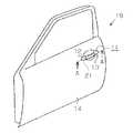
図2に示すように、車両ドア10にはアウトサイドハンドル11が設けられている。アウトサイドハンドル11は、車両ドア10の後部側に位置するように、該車両ドア10のドアアウタパネル14に取り付けられている。 As shown in FIG. 2, an
図3に示すように、前記アウトサイドハンドル11は、前記ドアアウタパネル14から車両の外側に突出するハンドル部(グリップ)12及びハンドルキャップ13を備えるとともに、車両ドア10の内部に位置するようにドアアウタパネル14に固定されるハンドルフレーム15を備えている。車両ドア10の開閉操作に際して、ハンドル部12が利用者(例えば、車両の所有者、運転者、搭乗者)によって握られて回動させられる。ハンドル部12とハンドルフレーム15との間にドアアウタパネル14を挟むようにして、ハンドル部12がハンドルフレーム15に対し所定の範囲で回動可能に連結されている。即ち、ハンドル部12の両端には、それぞれヒンジアーム12a及びストロークアーム12bが設けられている。上記ヒンジアーム12aはドアアウタパネル14を貫通するように延びて、ハンドルフレーム15に対し回動可能に連結されている。ストロークアーム12bはドアアウタパネル14を貫通するように延びて、ハンドルフレーム15に対し所定の範囲で移動可能なように係合されている。これにより、ハンドル部12は、ヒンジアーム12aを回動中心として、ストロークアーム12bによって許容される範囲でハンドルフレーム15に対し回動し得る。 As shown in FIG. 3, the
キーシリンダ16は、前記ハンドル部12に隣接するように前記ハンドルフレーム15に取り付けられている。前記ハンドルキャップ13は、このキーシリンダ16を包囲するように該キーシリンダ16に装着されている。すなわち、ハンドルキャップ13は、キーシリンダ16を介してハンドルフレーム15に固定されている。 The
前記車両ドア10に対する利用者の解錠/施錠の意志を認識して該車両ドアの解錠/施錠を制御する電子キーシステムは、車両に搭載された装置(車載機20)と利用者が携帯する携帯機(図示せず)とを備えている。 An electronic key system that recognizes the user's intention to unlock / lock the
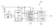
図4に示すように、前記車載機20は、送受信用アンテナ21と、送受信用駆動回路(通信用駆動回路)22と、センサ電極23と、静電容量検出装置24と、ドアロック装置25と、制御部26とを備えている。送受信用アンテナ21と、送受信用駆動回路22と、センサ電極23と、静電容量検出装置24とはアンテナ装置30を構成している。アンテナ装置30及び前記アウトサイドハンドル11は、ドアハンドル装置を構成している。送受信用駆動回路22、静電容量検出装置24、及び制御部26には、車載バッテリ27から電力が供給される。 As shown in FIG. 4, the in-
前記送受信用アンテナ21は、前記アウトサイドハンドル11内に収容されており(図3参照)、前記送受信用駆動回路22を介して前記制御部26に接続されている。送受信用アンテナ21は車室内外からの電波(レスポンス信号)を受信すると共に車室外に電気信号としての電波(リクエスト信号)を送信する。送受信用アンテナ21は車両ドア10の外側に配置されたアウトサイドハンドル11内に設けられているので、送受信用アンテナ21は電波を、金属製の車両ボディによって遮られることなく、所望の放射パターンで車両外側に向かって好適に放射し得る。 The transmission /
前記送受信用駆動回路22は前記制御部26に接続されている。送受信用駆動回路22は、制御部26によって制御され、利用者が携帯する携帯機が制御部26のメモリ26aに登録された識別情報(識別コード)を付与された携帯機であるかを認識すべく、送受信用アンテナ21を通じてリクエスト信号を送信する。携帯機は、リクエスト信号を受信すると、自身に付与された識別情報を含むレスポンス信号を送信する。送受信用駆動回路22は、携帯機からのレスポンス信号を送受信用アンテナ21を通じて受信すると、そのリクエスト信号を制御部26に伝送する。 The transmission /
前記センサ電極23は、前記静電容量検出装置24を介して前記制御部26に接続されている。センサ電極23と静電容量検出装置24とは静電容量式のセンサシステムを構成しており、利用者がアウトサイドハンドル11に接触したことを検出する。静電容量検出装置24は、制御部26によって制御され、センサ電極23とそれに対向する導体との間での静電容量の変化、即ちセンサ電極23とドアアウタパネル14との間若しくはセンサ電極23と地面との間での静電容量の変化を検出すると、利用者の手がハンドル部12に接触したことを示す信号を制御部26に伝送する。 The
前記制御部26は、送受信用駆動回路22、静電容量検出装置24、及びドアロック装置25等を制御する。制御部26は各種信号の授受に基づいてドアロック装置25を駆動して車両ドア10の解錠/施錠を行う。 The
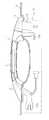
図3に示すように、前記ハンドル部12は中空状をなしており、このハンドル部12の内部に前記送受信用アンテナ21が収容されている。送受信用アンテナ21は、ハンドル部12内において機械的に固定されている。 As shown in FIG. 3, the
図1に示すように、前記送受信用アンテナ21は、コア31と該コア31に導線を巻回してなるコイル32とを備え、ループアンテナの形態をなしている。 As shown in FIG. 1, the transmission /
コア31は、アモルファス合金にて形成された複数枚のコアシート31aを、該コアシート31aの厚さ方向に間隔を有して積層することによって構成されている。複数枚のコアシート31aのうち一枚は、前記センサ電極23として利用される。例えば、本第1実施形態では、図1において最上部に位置するコアシート31aがセンサ電極23として利用される。 The
コイル32の両端部から延びる導線33,34は前記送受信用駆動回路22に接続されている。前記静電容量検出装置24から延びる導線35は、コイル32と送受信用駆動回路22との間を延びる両導線33,34のうちの一方、すなわち導線33に接続されている。よって、静電容量検出装置24は、導線35及び導線33を介してコイル32に電気的に接続されている。従って、静電容量検出装置24は、コイル32と前記センサ電極23との間に生じる寄生容量C1によって、センサ電極23と交流的に接続される。
次に、携帯機および車載機20を含む電子キーシステムの動作について説明する。 Next, the operation of the electronic key system including the portable device and the in-
例えば車両駐車時においては、車載機20の制御部26は、送受信用駆動回路22を駆動して、送受信用アンテナ21を通じて車外に電波(リクエスト信号)を送信させている。この状態で、携帯機を携帯した利用者が乗車のために車両に接近すると、携帯機は車両からのリクエスト信号を受信する。すると携帯機は、自身に付与された識別情報(識別コード)を含む電波(レスポンス信号)を送信する。 For example, when the vehicle is parked, the
車載機20においては、携帯機からのレスポンス信号が送受信用アンテナ21にて受信されて、制御部26に伝送される。制御部26は、このレスポンス信号の受信に基づき車両に携帯機が近づいてきたことを認識すると共に、レスポンス信号に含まれる識別情報をメモリ26aに予め記憶された識別情報と照合する。 In the in-
レスポンス信号に含まれる識別情報がメモリ26aに記憶された識別情報と一致する場合には、制御部26は、車両ドア10に対する利用者の解錠の意志を確認するためのドア解錠要求検出モードに移行する。ドア解錠要求検出モードでは、制御部26は、静電容量検出装置24を通じて、センサ電極23における静電容量の変化を検出する。即ち、利用者がハンドル部12に手をかけると、センサ電極23とドアアウタパネル14との間、若しくは、センサ電極23と地面との間で静電容量が変化する。静電容量検出装置24は、この静電容量の変化を検出し、利用者の手がハンドル部12に接触したことを示す信号を制御部26に伝送する。制御部26は、この信号を受信すると、ドアロック装置25を駆動して車両ドア10を解錠させる。従って、利用者は車両ドア10を開放して車両に乗車することができる。 When the identification information included in the response signal matches the identification information stored in the
上記した本第1実施形態は、以下の利点を有する。 The first embodiment described above has the following advantages.
(1)前記静電容量検出装置24から延びる導線35は、コイル32を送受信用駆動回路22に接続するよう該コイル32から延びる導線33に接続されている。即ち、静電容量検出装置24はコイル32に接続されている。そのため、静電容量検出装置24とコアシート31aとは、コアシート31aとコイル32との間に生じる寄生容量C1によって交流的に接続され、該コアシート31aはセンサ電極23として機能することができる。即ち、コア31と静電容量検出装置24から延びる導線35との間に電気接続点を設けることなく、コア31と静電容量検出装置24とが電気的に接続され、それによってコア31を構成するコアシート31aの1枚をセンサ電極23として機能させることができる。よって、ハンドル部12内に収容すべき部品の点数が減少する。従って、アウトサイドハンドル11の大型化を防止することができると共に、アウトサイドハンドル11の形状の自由度を増すことができる。更に、コア31と導線35との間に電気接続点を設ける必要がないため、そのような電気接続点に防水のための構成を設けるという必要もなく、よって製造コストの増大が抑制される。 (1) The
(2)コア31は、アモルファス合金により形成された複数枚のコアシート31aから構成されている。アモルファス合金は、導電性を有すると共に、例えば鋼板や珪素鋼板より高い透磁性、且つ優れた高周波特性を有する。従って、アモルファス合金製のコアシート31aは、静電容量式センサシステムにおける高感度なセンサ電極23として好適に利用できる。また、アモルファス合金製のコア31は、送受信用アンテナ21の高性能化及び小型化に貢献する。これは、送受信用アンテナ21を収容するハンドル部12の一層の小型化を可能とすると共に、アウトサイドハンドル11の形状の自由度を一層増す。 (2) The
(3)前記静電容量検出装置24から延びる導線35は、コイル32から送受信用駆動回路22にまで延びる導線33に接続されている。これにより、静電容量検出装置24とセンサ電極23(コアシート31a)とは、センサ電極23とコイル32との間に生じる寄生容量C1によって交流的に接続される。静電容量検出装置24から延びる導線35は、送受信用駆動回路22の近くで導線33に接続されればよく、導線35をセンサ電極23の近く、即ちハンドル部12の内部に至るまで引き回す必要がない。よって、ハンドル部12内に収容される配線の量を極力少なくすることができ、ハンドル部12の更なる小型化が可能となると共に、アウトサイドハンドル11の形状の自由度が更に増す。 (3) The
(第2実施形態)
以下、本発明を具体化した第2実施形態を図面に従って説明する。尚、上記第1実施形態と同様の構成については同一の符号を付してその説明を省略する。(Second Embodiment)
Hereinafter, a second embodiment of the present invention will be described with reference to the drawings. In addition, about the structure similar to the said 1st Embodiment, the same code | symbol is attached | subjected and the description is abbreviate | omitted.
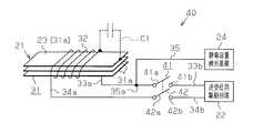
図5は本第2実施形態のアンテナ装置40を示す。図5に示すように、コイル32と送受信用駆動回路22とは、スイッチ41,42を介して接続されている。静電容量検出装置24から延びる導線35は、スイッチ41とコイル32との間を延びる導線33a上に接続点35aが位置するように、該導線33aに接続されている。これにより、静電容量検出装置24はコイル32に電気的に接続される。 FIG. 5 shows an
スイッチ41は、コイル32の一端から延びる前記導線33aに接続された可動端子41aと、送受信用駆動回路22から延びる導線33bに接続された接点41bとを含む。また、スイッチ42は、コイル32の他端から延びる導線34aに接続された可動端子42aと、送受信用駆動回路22から延びる導線34bに接続された接点42bとを含む。可動端子41a,42aの動作は制御部26によって制御される。即ち、制御部26は、送受信用駆動回路22を駆動させる際には、スイッチ41,42を閉路(オン)する。また、制御部26は、静電容量検出装置24を駆動させる際には、スイッチ41,42を開路(オフ)する。 The
図6は、前記送受信用駆動回路22に備えられる送信用駆動回路50の電気的構成を示す。送信用駆動回路50は、送受信用アンテナ21からリクエスト信号を送信する際に駆動される。図6に示すように、送信用駆動回路50は、キャリア信号(搬送波)を発振するキャリア発振回路51と、リクエスト信号のためのコード信号を生成するコード生成回路52と、AND回路53と、nチャネル形MOS(Metal Oxide Semiconductor)FET(Field Effect Transistor)54と、pチャネル形MOSFET55とを備えている。 FIG. 6 shows an electrical configuration of the
キャリア発振回路51はAND回路53の一方の入力端子に接続され、コード生成回路52はAND回路53の他方の入力端子に接続されている。AND回路53の出力端子は、nチャネル形MOSFET54のゲート及びpチャネル形MOSFET55のゲートに接続されている。 The carrier oscillation circuit 51 is connected to one input terminal of the AND
nチャネル形MOSFET54は、車載バッテリ27(図4参照)に接続されたソースと、コイル32(図5参照)に接続されたドレインとを有している。pチャネル形MOSFET55は、コイル32(図5参照)に接続されたドレインと、接地されたソースとを有している。即ち、nチャネル形MOSFET54とpチャネル形MOSFET55とは、相補形に組み合わせられてC(Complementary)−MOS(Metal Oxide Semiconductor)インバータを構成している。 The n-
制御部26(図4参照)は送信用駆動回路50を駆動して、キャリア発振回路51にキャリア信号を発振させるとともに、コード生成回路52にリクエスト信号のためのコード信号を生成させる。コード信号はキャリア信号に重畳されて送受信用アンテナ21に出力され、送受信用アンテナ21からリクエスト信号が送信される。 The control unit 26 (see FIG. 4) drives the
上記のように構成されたアンテナ装置40では、送信用駆動回路50にnチャネル形MOSFET54及びpチャネル形MOSFET55が備えられており、pチャネル形MOSFET55のソースが接地されている。nチャネル形MOSFET54におけるソースとドレインとの間には寄生容量C2が生じ、pチャネル形MOSFET55におけるソースとドレインとの間には寄生容量C3が生じる。 In the
ここで、図1に示す上記第1実施形態のアンテナ装置30の送受信用駆動回路22に、図6に示す送信用駆動回路50が備えられていると仮定する。図1のアンテナ装置30では、静電容量検出装置24から延びる導線35がコイル32から送受信用駆動回路22にまで延びる導線33に接続されているため、静電容量検出装置24はpチャネル形MOSFET55に生じる寄生容量C3を介して接地されることになる。また、一般的に、利用者がハンドル部12に接触した際に検出される静電容量の変化量は数pF程度である。これらのことから、センサ電極23にて検出される静電容量に比べてpチャネル形MOSFET55に生じる寄生容量C3が大きいと、センサ電極23においてコイル32が巻回された部分は利用者の手がハンドル部12に掛けられたことを検出することができない不感帯となる虞がある。また、pチャネル形MOSFET55の寄生容量C3は温度の変化等により変動する。この寄生容量C3の変動は、静電容量検出装置24における静電容量の検出感度のばらつきを招く原因の一つとなる。 Here, it is assumed that the transmission /
これに対し、図5に示す本第2実施形態のアンテナ装置40では、送受信用駆動回路22とコイル32とはスイッチ41,42を介して接続されている。スイッチ41,42は、静電容量検出装置24が駆動される際には、制御部26にて開路(オフ)される。即ち、静電容量検出装置24は、図6の送信用駆動回路50を備えた送受信用駆動回路22から機械的に切り離される。従って、制御部26によって静電容量検出装置24が駆動される際、pチャネル形MOSFET55に生じる寄生容量C3の大きさに関わらず、静電容量検出装置24にて検出される静電容量はpチャネル形MOSFET55に生じる寄生容量C3の影響を受けない。そのため、センサ電極23においてコイル32が巻回されている部分が不感帯となることが防止される。 In contrast, in the
上記した本第2実施形態は、第1実施形態が有する上記利点の(1)及び(2)と同様の利点に加えて、以下の利点を有する。 The second embodiment described above has the following advantages in addition to the advantages (1) and (2) of the advantages of the first embodiment.
(1)コイル32は、スイッチ41,42を開路することにより、送信用駆動回路50から切り離される。従って、送信用駆動回路50が、ソースとドレインとの間に寄生容量C3を生じ且つソースが接地されたpチャネル形MOSFET55を備えている場合であっても、寄生容量C3の大きさに関わらず、センサ電極23においてコイル32が巻回された部分が不感帯となることを防止することができる。その結果、利用者がハンドル部12に接触したことを検出できないといった不具合が発生することを防止することができる。尚、送受信用アンテナ21からリクエスト信号を受信する場合や、同送受信用アンテナ21からレスポンス信号を送信する場合には、スイッチ41,42を閉路すればよい。 (1) The
(第3実施形態)
以下、本発明を具体化した第3実施形態を図面に従って説明する。尚、上記第1及び第2実施形態と同様の構成については同一の符号を付してその説明を省略する。(Third embodiment)
Hereinafter, a third embodiment of the present invention will be described with reference to the drawings. In addition, about the structure similar to the said 1st and 2nd embodiment, the same code | symbol is attached | subjected and the description is abbreviate | omitted.
図7は本第3実施形態のアンテナ装置60を示す。本第3実施形態のアンテナ装置60は、上記第2実施形態の送受信用駆動回路22と同様に、図6に示す送信用駆動回路50を備えている。図7に示すように、コイル32と送受信用駆動回路22とは、トランス61を介して接続されている。トランス61は、コイル32と送受信用駆動回路22とを、交流的には接続するが、直流的には切り離す。静電容量検出装置24から延びる導線35は、トランス61とコイル32との間を延びる導線33a上に接続点35aが位置するように、該導線33aに接続されている。これにより、静電容量検出装置24はコイル32と電気的に接続される。 FIG. 7 shows an
このように構成されたアンテナ装置60においては、静電容量検出装置24が、送信用駆動回路50を備えた送受信用駆動回路22から直流的に切り離される。そのため、pチャネル形MOSFET55の寄生容量C3の大きさに関わらず、静電容量検出装置24にて検出される静電容量はpチャネル形MOSFET55の寄生容量C3の影響を受けない。従って、センサ電極23においてコイル32が巻回された部分が不感帯となることが防止される。 In the
上記した本第3実施形態は、第1実施形態の上記利点の(1)及び(2)と同様の利点に加えて、以下の利点を有する。 The third embodiment described above has the following advantages in addition to the advantages similar to the advantages (1) and (2) of the first embodiment.
(1)コイル32と送信用駆動回路50とはトランス61を介して接続されているため、コイル32と送受信用駆動回路22とは、交流的には接続され、直流的には切り離される。また、トランス61は、静電容量検出装置24を送信用駆動回路50から直流的に切り離す。従って、送信用駆動回路50が、ソースとドレインとの間に寄生容量C3を生じ且つソースが接地されたpチャネル形MOSFET55を備えている場合であっても、寄生容量C3の大きさに関わらず、センサ電極23においてコイル32が巻回された部分が不感帯となることを防止することができる。その結果、利用者がハンドル部12に接触したことを検出できないといった不具合が発生することを防止することができる。また、コイル32と送信用駆動回路50とはトランス61によって交流的には接続されているため、送受信用アンテナ21からリクエスト信号を受信する場合や、同送受信用アンテナ21からレスポンス信号を送信する場合に、上記第2実施形態のようにスイッチ41,42を制御するという必要がない。そのため、スイッチ41,42及びそれらを制御するための制御回路等が不要であり、アンテナ装置60の大型化が防止される。 (1) Since the
尚、本発明の実施形態は、以下のように変更してもよい。 In addition, you may change embodiment of this invention as follows.
上記各実施形態では、コア31を構成する複数枚のコアシート31aのうち、最上部に位置するコアシート31aをセンサ電極23として利用している。しかしこれに限らず、コア31を構成する複数枚のコアシート31aのうち、最上部以外に位置するいずれかのコアシート31aをセンサ電極として利用してもよい。 In each of the above-described embodiments, the
上記各実施形態では、コア31は、複数枚のコアシート31aを積層することによって形成されている。しかしこれに限らず、コア31は、例えば軟磁性金属粉体を圧縮成形してなるものであってもよい。この場合、コア31全体がセンサ電極として利用される。 In the above embodiments, the
上記各実施形態において、コア31はシール膜にて覆われていてもよい。このようにすると、コア31が腐食することが防止され、コア31の耐久性が向上する。 In each of the above embodiments, the
上記各実施形態では、コアシート31aはアモルファス合金にて形成されている。しかしこれに限らず、コアシート31aは、アモルファス合金以外の導電性合金にて形成されてもよい。 In each said embodiment, the
Claims (6)
Translated fromJapanese前記コアの少なくとも一部によって構成されるセンサ電極と、
前記コイルに電気的に接続され、前記センサ電極における静電容量の変化を検出する静電容量検出装置と
を備えたことを特徴とするアンテナ装置。An antenna comprising a core made of a conductive alloy and a coil wound around the core;
A sensor electrode constituted by at least a part of the core;
An antenna device comprising: a capacitance detection device that is electrically connected to the coil and detects a change in capacitance in the sensor electrode.
前記コイルに接続される通信用駆動回路を更に備え、
前記静電容量検出装置は、前記コイルと前記通信用駆動回路との間を延びる導線に接続されていることを特徴とするアンテナ装置。The antenna device according to claim 1,
A communication drive circuit connected to the coil;
The antenna device, wherein the capacitance detection device is connected to a conductive wire extending between the coil and the communication drive circuit.
前記コイルに接続され、前記アンテナから電気信号を送信させる送信用駆動回路と、
前記コイルと前記送信用駆動回路との間に設けられるスイッチとを更に備え、
前記静電容量検出装置は、前記コイルと前記スイッチとの間を延びる導線に接続されていることを特徴とするアンテナ装置。The antenna device according to claim 1,
A transmission drive circuit connected to the coil and transmitting an electrical signal from the antenna;
A switch provided between the coil and the transmission drive circuit;
The said capacitance detection apparatus is connected to the conducting wire extended between the said coil and the said switch, The antenna apparatus characterized by the above-mentioned.
前記コイルに接続され、前記アンテナから電気信号を送信させる送信用駆動回路と、
前記コイルと前記送信用駆動回路との間に設けられるトランスとを更に備え、
前記静電容量検出装置は、前記コイルと前記トランスとの間を延びる導線に接続されていることを特徴とするアンテナ装置。The antenna device according to claim 1,
A transmission drive circuit connected to the coil and transmitting an electrical signal from the antenna;
A transformer provided between the coil and the transmission drive circuit;
The capacitance detecting device is connected to a conductive wire extending between the coil and the transformer.
前記コアは、アモルファス合金にて形成されていることを特徴とするアンテナ装置。The antenna device according to any one of claims 1 to 4,
The antenna device, wherein the core is made of an amorphous alloy.
前記アンテナは前記ハンドル内に収容されることを特徴とするドアハンドル装置。In a door undle device provided with the antenna device according to any one of claims 1 to 5, and a handle arranged on the outside of a vehicle door,
The door handle device is characterized in that the antenna is housed in the handle.
Applications Claiming Priority (3)
| Application Number | Priority Date | Filing Date | Title |
|---|---|---|---|
| JP2004282501 | 2004-09-28 | ||
| JP2004282501 | 2004-09-28 | ||
| PCT/JP2005/017188WO2006035623A1 (en) | 2004-09-28 | 2005-09-16 | Antenna assembly and door handle unit |
Publications (2)
| Publication Number | Publication Date |
|---|---|
| JPWO2006035623A1 JPWO2006035623A1 (en) | 2008-05-15 |
| JP4428388B2true JP4428388B2 (en) | 2010-03-10 |
Family
ID=36118775
Family Applications (1)
| Application Number | Title | Priority Date | Filing Date |
|---|---|---|---|
| JP2006537682AExpired - Fee RelatedJP4428388B2 (en) | 2004-09-28 | 2005-09-16 | Antenna device and door handle device |
Country Status (4)
| Country | Link |
|---|---|
| US (1) | US7679571B2 (en) |
| EP (1) | EP1795860B1 (en) |
| JP (1) | JP4428388B2 (en) |
| WO (1) | WO2006035623A1 (en) |
Families Citing this family (25)
| Publication number | Priority date | Publication date | Assignee | Title |
|---|---|---|---|---|
| JP4428388B2 (en) | 2004-09-28 | 2010-03-10 | アイシン精機株式会社 | Antenna device and door handle device |
| WO2007092240A2 (en)* | 2006-02-02 | 2007-08-16 | Xpresense Llc | Rf-based dynamic remote control device based on generating and sensing of electrical field in vicinity of the operator |
| DE102006013027B4 (en)* | 2006-03-20 | 2008-03-20 | SCHÜCO International KG | handle element |
| JP5170087B2 (en)* | 2007-04-13 | 2013-03-27 | 株式会社村田製作所 | Portable electronic devices |
| JP4751860B2 (en)* | 2007-07-27 | 2011-08-17 | アイシン精機株式会社 | Door handle device |
| DE102008027160A1 (en)* | 2008-06-06 | 2009-12-10 | Conti Temic Microelectronic Gmbh | Electronic locking system for locking vehicle, has energy generating unit electromechanically and/or electromagnetically connected to manually operable actuating unit, and generating electrical energy during operation of actuating unit |
| DE102009034033A1 (en)* | 2009-07-21 | 2011-01-27 | Huf Hülsbeck & Fürst Gmbh & Co. Kg | Door opening and/or closing device control method for vehicle, involves transferring controller into switched on active condition after receiving signal, and transferring handle into operative position during correlation |
| JP5496335B2 (en)* | 2010-07-21 | 2014-05-21 | アルプス電気株式会社 | Electronic equipment with wireless communication function |
| JP5666289B2 (en)* | 2010-12-24 | 2015-02-12 | 京セラ株式会社 | Electronics |
| DE102011080185A1 (en)* | 2011-08-01 | 2013-02-07 | BSH Bosch und Siemens Hausgeräte GmbH | Home appliance with antenna |
| FR2998235B1 (en)* | 2012-11-19 | 2016-02-26 | Continental Automotive France | DEVICE FOR DETECTING A "HAND FREE" ACCESS BADGE AROUND A VEHICLE AND DETECTING THE PRESENCE OF A USER NEAR AN OPENING OF A VEHICLE AND DETECTION METHOD THEREOF |
| DE102013102701A1 (en)* | 2013-03-18 | 2014-09-18 | Huf Hülsbeck & Fürst Gmbh & Co. Kg | Door handle assembly for a motor vehicle with capacitive proximity sensor and NFC transmitter / receiver unit |
| TWI464318B (en)* | 2013-07-29 | 2014-12-11 | Univ Nat Taipei Technology | Sensing device installed in a handle and vehicle door handle |
| DE102015111767A1 (en)* | 2014-07-18 | 2016-01-21 | Huf Hülsbeck & Fürst Gmbh & Co. Kg | Door interior handle system for a door of a vehicle |
| DE102014218213B4 (en)* | 2014-09-11 | 2017-09-28 | Continental Automotive Gmbh | Arrangement and method for detecting the approach of an object |
| DE102014113832A1 (en) | 2014-09-24 | 2016-03-24 | Huf Hülsbeck & Fürst Gmbh & Co. Kg | Data and measuring device for a door handle and method therefor |
| WO2016062338A1 (en)* | 2014-10-22 | 2016-04-28 | Abb Technology Ltd | A control unit comprising an antenna for wireless communication with a remote unit |
| JP6700585B2 (en)* | 2016-02-29 | 2020-05-27 | アイシン精機株式会社 | Antenna module |
| TWI597624B (en)* | 2016-06-03 | 2017-09-01 | 凌通科技股份有限公司 | Integrated communication and capacitive sensing circuit and interactive system using the same |
| DE102017110144A1 (en)* | 2017-04-28 | 2018-10-31 | Huf Hülsbeck & Fürst Gmbh & Co. Kg | Authentication system of a vehicle |
| FR3083877B1 (en)* | 2018-07-12 | 2020-06-12 | Continental Automotive France | ACTIVATION MODULE SIMULTANEOUSLY DETECTING AN APPROACH AND SUPPORT OF A USER WITH A MOBILE HIGH FREQUENCY ANTENNA |
| DE102018122254B3 (en) | 2018-09-12 | 2019-12-12 | Ifm Electronic Gmbh | Capacitive door handle sensor with an antenna for near field communication |
| EP3945501B1 (en)* | 2020-07-31 | 2023-05-03 | Continental Automotive Technologies GmbH | Access system |
| FR3127007B1 (en)* | 2021-09-16 | 2024-07-12 | Vitesco Technologies | Sensor for controlling access to a motor vehicle, with an electrode surrounded by an antenna. |
| US11894885B2 (en)* | 2022-05-23 | 2024-02-06 | Qualcomm Incorporated | Near ultra low energy field transducer design |
Family Cites Families (64)
| Publication number | Priority date | Publication date | Assignee | Title |
|---|---|---|---|---|
| GB995314A (en) | 1962-09-23 | 1965-06-16 | Sato Yoshio | Improvements in or relating to aerials |
| JPS5924533A (en) | 1982-07-30 | 1984-02-08 | Hashimoto Forming Co Ltd | Manufacture of bent product of hollow material |
| JPS60233904A (en) | 1984-05-04 | 1985-11-20 | Matsushita Electric Ind Co Ltd | Antenna system |
| CA1245352A (en)* | 1984-11-26 | 1988-11-22 | Junzo Ohe | Automobile antenna system |
| JPS6231201A (en)* | 1985-08-01 | 1987-02-10 | Dx Antenna Co Ltd | Microstrip antenna system |
| JPH0642605B2 (en)* | 1985-08-09 | 1994-06-01 | トヨタ自動車株式会社 | Car antenna device |
| JPS62216409A (en)* | 1986-03-17 | 1987-09-24 | Aisin Seiki Co Ltd | Antenna unit |
| JPS6367903A (en)* | 1986-09-10 | 1988-03-26 | Aisin Seiki Co Ltd | Antenna system |
| JPS6387806A (en)* | 1986-09-30 | 1988-04-19 | Aisin Seiki Co Ltd | Circularly polarized wave microstrip antenna |
| JPS63115403A (en) | 1986-10-31 | 1988-05-20 | Matsushita Electric Ind Co Ltd | Bar antenna |
| JP2662567B2 (en)* | 1987-09-25 | 1997-10-15 | アイシン精機株式会社 | Three-resonance microstrip antenna device |
| US4990927A (en)* | 1988-03-25 | 1991-02-05 | Takashi Nakamura | Microstrip antenna |
| US5173712A (en)* | 1988-06-17 | 1992-12-22 | Aisin Seiki K.K. | Rod antenna with filter arrangement |
| JPH0254415A (en) | 1988-08-18 | 1990-02-23 | Victor Co Of Japan Ltd | Magnetic recording and reproducing device for information signal |
| JPH0269908A (en) | 1988-09-05 | 1990-03-08 | Mitsui Petrochem Ind Ltd | Capacitor and inductor |
| US4916582A (en)* | 1988-12-20 | 1990-04-10 | Murata Manufacturing Co., Ltd. | Electronic component and its production method |
| JPH03285402A (en)* | 1990-03-31 | 1991-12-16 | Aisin Seiki Co Ltd | Antenna device for automobile |
| US5497165A (en)* | 1990-12-14 | 1996-03-05 | Aisin Seiki Kabushiki Kaisha | Microstrip antenna |
| US5541615A (en)* | 1991-07-31 | 1996-07-30 | Aisin Seiki Kabushiki Kaisha | 3 band communication equipment |
| JP3282082B2 (en)* | 1992-03-26 | 2002-05-13 | アイシン精機株式会社 | Circularly polarized linear antenna |
| JPH0751788A (en) | 1993-08-11 | 1995-02-28 | Aida Eng Ltd | Plastic working method for gear or gear-like material |
| JPH10292702A (en)* | 1997-04-21 | 1998-11-04 | Aisin Seiki Co Ltd | Door proximity communication device and door lock control device |
| JPH10317747A (en) | 1997-05-20 | 1998-12-02 | Alpha Corp | Keyless entry device |
| US6768413B1 (en)* | 1997-10-14 | 2004-07-27 | Huf Hülsbeck & Fürst Gmbh & Co. Kg | Closing device, in particular for motor vehicles |
| WO1999046784A1 (en) | 1998-03-13 | 1999-09-16 | Matsushita Electric Industrial Co., Ltd. | Module and method of manufacture |
| JP4167320B2 (en) | 1998-03-31 | 2008-10-15 | 富士通テン株式会社 | Wireless control device for vehicle and portable device thereof |
| DE10107319A1 (en)* | 2000-02-18 | 2002-01-31 | Aisin Seiki | Loop antenna device |
| JP3714129B2 (en) | 2000-07-14 | 2005-11-09 | アイシン精機株式会社 | Door opener |
| JP3509790B2 (en)* | 2000-08-09 | 2004-03-22 | アイシン精機株式会社 | Vehicle door lock device |
| JP2002057564A (en)* | 2000-08-11 | 2002-02-22 | Aisin Seiki Co Ltd | Human body detector |
| JP2002106214A (en) | 2000-09-28 | 2002-04-10 | Calsonic Kansei Corp | Door opening motion detecting method and device for vehicle |
| JP2002252521A (en)* | 2001-02-23 | 2002-09-06 | Aisin Seiki Co Ltd | Loop antenna device |
| DE10163778B4 (en)* | 2001-06-27 | 2008-01-24 | Witte-Velbert Gmbh & Co. Kg | Handle with integrated antenna and sensor electrode |
| JP3566943B2 (en)* | 2001-07-02 | 2004-09-15 | アイシン精機株式会社 | Vehicle door handle |
| JP3646077B2 (en) | 2001-07-05 | 2005-05-11 | 株式会社ホンダロック | In-vehicle device remote control device |
| DE60223405T2 (en)* | 2001-10-01 | 2008-08-21 | Donnelly Corp., Holland | VEHICLE GRIP ASSEMBLY WITH ANTENNA |
| JP4064094B2 (en) | 2001-11-26 | 2008-03-19 | トヨタ自動車株式会社 | Vehicle periphery monitoring device |
| JP3882595B2 (en)* | 2001-11-28 | 2007-02-21 | アイシン精機株式会社 | Antenna device |
| JP4003453B2 (en)* | 2001-12-26 | 2007-11-07 | アイシン精機株式会社 | Human body detection device |
| JP2003214004A (en)* | 2002-01-24 | 2003-07-30 | Aisin Seiki Co Ltd | Door lock control method and door lock device |
| JP2003283231A (en)* | 2002-03-26 | 2003-10-03 | Aisin Seiki Co Ltd | Antenna and manufacturing method thereof |
| JP3901034B2 (en) | 2002-06-24 | 2007-04-04 | アイシン精機株式会社 | Vehicle door opening and closing device |
| JP2004060191A (en)* | 2002-07-25 | 2004-02-26 | Aisin Seiki Co Ltd | Vehicle door handle |
| JP3770218B2 (en)* | 2002-08-29 | 2006-04-26 | アイシン精機株式会社 | Human body detection device for vehicle door opening and method of using the same |
| JP2004232300A (en)* | 2003-01-29 | 2004-08-19 | Aisin Seiki Co Ltd | Outside handle device |
| JP2004239008A (en)* | 2003-02-07 | 2004-08-26 | Furukawa Electric Co Ltd:The | Outside handle device and connector used therefor |
| JP2004257126A (en)* | 2003-02-26 | 2004-09-16 | Aisin Seiki Co Ltd | Vehicle door opening and closing device |
| US7057124B2 (en)* | 2003-04-22 | 2006-06-06 | Aisin Seiki Kabushiki Kaisha | Push switch apparatus |
| JP2004346703A (en)* | 2003-05-26 | 2004-12-09 | Aisin Seiki Co Ltd | Antenna element with sensor, door handle device |
| JP3826897B2 (en)* | 2003-04-22 | 2006-09-27 | アイシン精機株式会社 | Antenna device with sensor, door handle device |
| EP1617509A4 (en) | 2003-04-22 | 2006-05-31 | Aisin Seiki | Electrostatic capacity type sensor-carrying antenna device |
| JP4348993B2 (en)* | 2003-04-24 | 2009-10-21 | アイシン精機株式会社 | Electrical component and manufacturing method thereof |
| US7319599B2 (en)* | 2003-10-01 | 2008-01-15 | Matsushita Electric Industrial Co., Ltd. | Module incorporating a capacitor, method for manufacturing the same, and capacitor used therefor |
| JP2005113475A (en)* | 2003-10-07 | 2005-04-28 | Aisin Seiki Co Ltd | Door handle device |
| JP4098215B2 (en)* | 2003-10-29 | 2008-06-11 | アイシン精機株式会社 | Human body detection device for vehicle |
| JP4052277B2 (en)* | 2004-04-19 | 2008-02-27 | アイシン精機株式会社 | Vehicle door handle device |
| JP4310699B2 (en)* | 2004-06-22 | 2009-08-12 | アイシン精機株式会社 | Switch device |
| JP4240307B2 (en)* | 2004-06-22 | 2009-03-18 | アイシン精機株式会社 | Vehicle door opening and closing device |
| JP4257601B2 (en)* | 2004-06-24 | 2009-04-22 | アイシン精機株式会社 | Vehicle door opening and closing device |
| JP4428388B2 (en) | 2004-09-28 | 2010-03-10 | アイシン精機株式会社 | Antenna device and door handle device |
| JP4513481B2 (en) | 2004-09-28 | 2010-07-28 | アイシン精機株式会社 | Antenna device and door handle device |
| JP4337742B2 (en)* | 2005-01-26 | 2009-09-30 | アイシン精機株式会社 | Antenna device |
| JP4947348B2 (en)* | 2006-09-13 | 2012-06-06 | アイシン精機株式会社 | Vehicle door handle device |
| JP4655230B2 (en)* | 2006-09-20 | 2011-03-23 | アイシン精機株式会社 | Bobbin for bar antenna, bar antenna and vehicle door handle |
- 2005
- 2005-09-16JPJP2006537682Apatent/JP4428388B2/ennot_activeExpired - Fee Related
- 2005-09-16USUS11/661,595patent/US7679571B2/ennot_activeExpired - Fee Related
- 2005-09-16EPEP20050783396patent/EP1795860B1/ennot_activeCeased
- 2005-09-16WOPCT/JP2005/017188patent/WO2006035623A1/enactiveApplication Filing
Also Published As
| Publication number | Publication date |
|---|---|
| EP1795860B1 (en) | 2012-11-14 |
| JPWO2006035623A1 (en) | 2008-05-15 |
| WO2006035623A1 (en) | 2006-04-06 |
| EP1795860A4 (en) | 2010-03-31 |
| US7679571B2 (en) | 2010-03-16 |
| US20080100522A1 (en) | 2008-05-01 |
| EP1795860A1 (en) | 2007-06-13 |
Similar Documents
| Publication | Publication Date | Title |
|---|---|---|
| JP4428388B2 (en) | Antenna device and door handle device | |
| JP4161664B2 (en) | Vehicle door handle device | |
| EP1006028A2 (en) | Door handle for vehicle and smart entry system for vehicle using the same | |
| JP5589870B2 (en) | Vehicle door handle device | |
| CN101529654B (en) | Antenna device | |
| JP5109172B2 (en) | Transmitting antenna device and door handle in which transmitting antenna device is accommodated | |
| JP2001520337A (en) | Closing devices, especially for motor vehicles | |
| JP3696866B2 (en) | Door opener | |
| JP5050223B2 (en) | Transmission / reception antenna device and signal transmission system | |
| CN107435471A (en) | A kind of door handle and Anneta module | |
| US20040257296A1 (en) | Door handle for a vehicle | |
| JP2006083522A (en) | Door handle device and keyless entry device provided with the same | |
| CN100536227C (en) | Vehiclar antenna device, antenna system and communication system using the same for vehicle | |
| CN1973105A (en) | Vehicle handle | |
| JP4513481B2 (en) | Antenna device and door handle device | |
| JP2010010916A (en) | Antenna device and door handle where the antenna device is to be housed | |
| JP3826881B2 (en) | Vehicle door handle device | |
| JP2009194796A (en) | Portable machine | |
| JP2004225350A (en) | Remote control unit for keyless entry system | |
| JP3639292B1 (en) | Door opener | |
| JP4638814B2 (en) | Communication device | |
| WO2016157773A1 (en) | Coil unit | |
| JP4107185B2 (en) | Vehicle antenna device and communication system using the same | |
| JP7017387B2 (en) | Proximity sensor and keyless entry device equipped with it | |
| JP2010031455A (en) | Electronic key system |
Legal Events
| Date | Code | Title | Description |
|---|---|---|---|
| A621 | Written request for application examination | Free format text:JAPANESE INTERMEDIATE CODE: A621 Effective date:20080828 | |
| TRDD | Decision of grant or rejection written | ||
| A01 | Written decision to grant a patent or to grant a registration (utility model) | Free format text:JAPANESE INTERMEDIATE CODE: A01 Effective date:20091124 | |
| A01 | Written decision to grant a patent or to grant a registration (utility model) | Free format text:JAPANESE INTERMEDIATE CODE: A01 | |
| FPAY | Renewal fee payment (event date is renewal date of database) | Free format text:PAYMENT UNTIL: 20121225 Year of fee payment:3 | |
| R151 | Written notification of patent or utility model registration | Ref document number:4428388 Country of ref document:JP Free format text:JAPANESE INTERMEDIATE CODE: R151 | |
| A61 | First payment of annual fees (during grant procedure) | Free format text:JAPANESE INTERMEDIATE CODE: A61 Effective date:20091207 | |
| FPAY | Renewal fee payment (event date is renewal date of database) | Free format text:PAYMENT UNTIL: 20121225 Year of fee payment:3 | |
| FPAY | Renewal fee payment (event date is renewal date of database) | Free format text:PAYMENT UNTIL: 20131225 Year of fee payment:4 | |
| LAPS | Cancellation because of no payment of annual fees |