JP4426632B2 - Plasma processing equipment - Google Patents
Plasma processing equipmentDownload PDFInfo
- Publication number
- JP4426632B2 JP4426632B2JP2008551375AJP2008551375AJP4426632B2JP 4426632 B2JP4426632 B2JP 4426632B2JP 2008551375 AJP2008551375 AJP 2008551375AJP 2008551375 AJP2008551375 AJP 2008551375AJP 4426632 B2JP4426632 B2JP 4426632B2
- Authority
- JP
- Japan
- Prior art keywords
- gas
- source gas
- substrate stage
- plasma
- source
- Prior art date
- Legal status (The legal status is an assumption and is not a legal conclusion. Google has not performed a legal analysis and makes no representation as to the accuracy of the status listed.)
- Expired - Fee Related
Links
Images


Classifications
- C—CHEMISTRY; METALLURGY
- C23—COATING METALLIC MATERIAL; COATING MATERIAL WITH METALLIC MATERIAL; CHEMICAL SURFACE TREATMENT; DIFFUSION TREATMENT OF METALLIC MATERIAL; COATING BY VACUUM EVAPORATION, BY SPUTTERING, BY ION IMPLANTATION OR BY CHEMICAL VAPOUR DEPOSITION, IN GENERAL; INHIBITING CORROSION OF METALLIC MATERIAL OR INCRUSTATION IN GENERAL
- C23C—COATING METALLIC MATERIAL; COATING MATERIAL WITH METALLIC MATERIAL; SURFACE TREATMENT OF METALLIC MATERIAL BY DIFFUSION INTO THE SURFACE, BY CHEMICAL CONVERSION OR SUBSTITUTION; COATING BY VACUUM EVAPORATION, BY SPUTTERING, BY ION IMPLANTATION OR BY CHEMICAL VAPOUR DEPOSITION, IN GENERAL
- C23C16/00—Chemical coating by decomposition of gaseous compounds, without leaving reaction products of surface material in the coating, i.e. chemical vapour deposition [CVD] processes
- C23C16/22—Chemical coating by decomposition of gaseous compounds, without leaving reaction products of surface material in the coating, i.e. chemical vapour deposition [CVD] processes characterised by the deposition of inorganic material, other than metallic material
- C23C16/30—Deposition of compounds, mixtures or solid solutions, e.g. borides, carbides, nitrides
- C23C16/40—Oxides
- C23C16/401—Oxides containing silicon
- C23C16/402—Silicon dioxide
- C—CHEMISTRY; METALLURGY
- C23—COATING METALLIC MATERIAL; COATING MATERIAL WITH METALLIC MATERIAL; CHEMICAL SURFACE TREATMENT; DIFFUSION TREATMENT OF METALLIC MATERIAL; COATING BY VACUUM EVAPORATION, BY SPUTTERING, BY ION IMPLANTATION OR BY CHEMICAL VAPOUR DEPOSITION, IN GENERAL; INHIBITING CORROSION OF METALLIC MATERIAL OR INCRUSTATION IN GENERAL
- C23C—COATING METALLIC MATERIAL; COATING MATERIAL WITH METALLIC MATERIAL; SURFACE TREATMENT OF METALLIC MATERIAL BY DIFFUSION INTO THE SURFACE, BY CHEMICAL CONVERSION OR SUBSTITUTION; COATING BY VACUUM EVAPORATION, BY SPUTTERING, BY ION IMPLANTATION OR BY CHEMICAL VAPOUR DEPOSITION, IN GENERAL
- C23C16/00—Chemical coating by decomposition of gaseous compounds, without leaving reaction products of surface material in the coating, i.e. chemical vapour deposition [CVD] processes
- C23C16/44—Chemical coating by decomposition of gaseous compounds, without leaving reaction products of surface material in the coating, i.e. chemical vapour deposition [CVD] processes characterised by the method of coating
- C23C16/455—Chemical coating by decomposition of gaseous compounds, without leaving reaction products of surface material in the coating, i.e. chemical vapour deposition [CVD] processes characterised by the method of coating characterised by the method used for introducing gases into reaction chamber or for modifying gas flows in reaction chamber
- C23C16/45519—Inert gas curtains
- C—CHEMISTRY; METALLURGY
- C23—COATING METALLIC MATERIAL; COATING MATERIAL WITH METALLIC MATERIAL; CHEMICAL SURFACE TREATMENT; DIFFUSION TREATMENT OF METALLIC MATERIAL; COATING BY VACUUM EVAPORATION, BY SPUTTERING, BY ION IMPLANTATION OR BY CHEMICAL VAPOUR DEPOSITION, IN GENERAL; INHIBITING CORROSION OF METALLIC MATERIAL OR INCRUSTATION IN GENERAL
- C23C—COATING METALLIC MATERIAL; COATING MATERIAL WITH METALLIC MATERIAL; SURFACE TREATMENT OF METALLIC MATERIAL BY DIFFUSION INTO THE SURFACE, BY CHEMICAL CONVERSION OR SUBSTITUTION; COATING BY VACUUM EVAPORATION, BY SPUTTERING, BY ION IMPLANTATION OR BY CHEMICAL VAPOUR DEPOSITION, IN GENERAL
- C23C16/00—Chemical coating by decomposition of gaseous compounds, without leaving reaction products of surface material in the coating, i.e. chemical vapour deposition [CVD] processes
- C23C16/44—Chemical coating by decomposition of gaseous compounds, without leaving reaction products of surface material in the coating, i.e. chemical vapour deposition [CVD] processes characterised by the method of coating
- C23C16/50—Chemical coating by decomposition of gaseous compounds, without leaving reaction products of surface material in the coating, i.e. chemical vapour deposition [CVD] processes characterised by the method of coating using electric discharges
- C23C16/505—Chemical coating by decomposition of gaseous compounds, without leaving reaction products of surface material in the coating, i.e. chemical vapour deposition [CVD] processes characterised by the method of coating using electric discharges using radio frequency discharges
- H—ELECTRICITY
- H01—ELECTRIC ELEMENTS
- H01J—ELECTRIC DISCHARGE TUBES OR DISCHARGE LAMPS
- H01J37/00—Discharge tubes with provision for introducing objects or material to be exposed to the discharge, e.g. for the purpose of examination or processing thereof
- H01J37/32—Gas-filled discharge tubes
- H01J37/32431—Constructional details of the reactor
- H01J37/3244—Gas supply means
- H—ELECTRICITY
- H01—ELECTRIC ELEMENTS
- H01J—ELECTRIC DISCHARGE TUBES OR DISCHARGE LAMPS
- H01J37/00—Discharge tubes with provision for introducing objects or material to be exposed to the discharge, e.g. for the purpose of examination or processing thereof
- H01J37/32—Gas-filled discharge tubes
- H01J37/32431—Constructional details of the reactor
- H01J37/32458—Vessel
- H01J37/32477—Vessel characterised by the means for protecting vessels or internal parts, e.g. coatings
- H01J37/32495—Means for protecting the vessel against plasma
- H—ELECTRICITY
- H05—ELECTRIC TECHNIQUES NOT OTHERWISE PROVIDED FOR
- H05H—PLASMA TECHNIQUE; PRODUCTION OF ACCELERATED ELECTRICALLY-CHARGED PARTICLES OR OF NEUTRONS; PRODUCTION OR ACCELERATION OF NEUTRAL MOLECULAR OR ATOMIC BEAMS
- H05H1/00—Generating plasma; Handling plasma
- H05H1/24—Generating plasma
- H05H1/46—Generating plasma using applied electromagnetic fields, e.g. high frequency or microwave energy
Landscapes
- Chemical & Material Sciences (AREA)
- Engineering & Computer Science (AREA)
- Physics & Mathematics (AREA)
- Plasma & Fusion (AREA)
- Materials Engineering (AREA)
- Mechanical Engineering (AREA)
- Metallurgy (AREA)
- Organic Chemistry (AREA)
- Chemical Kinetics & Catalysis (AREA)
- General Chemical & Material Sciences (AREA)
- Analytical Chemistry (AREA)
- Electromagnetism (AREA)
- Spectroscopy & Molecular Physics (AREA)
- Inorganic Chemistry (AREA)
- Chemical Vapour Deposition (AREA)
- Drying Of Semiconductors (AREA)
- Plasma Technology (AREA)
Description
Translated fromJapanese本発明は、半導体素子、フラットパネルディスプレイ、および太陽電池などの製造に用いられるプラズマ処理装置に関し、特に、成膜面積が大きい場合であっても、成膜速度を向上させるとともに、パーティクルの発生を抑制することができるプラズマ処理装置に関するものである。 The present invention relates to a plasma processing apparatus used in the manufacture of semiconductor elements, flat panel displays, solar cells, and the like, and in particular, improves film formation speed and generates particles even when the film formation area is large. The present invention relates to a plasma processing apparatus that can be suppressed.
今日、半導体素子、太陽電池、または液晶表示パネルもしくはプラズマディスプレイパネルなどのフラットパネルディスプレイの製造には、エッチング、スパッタリングまたはCVD(Chemical Vapor Deposition)等が利用されて、精度の高い加工処理が行なわれている。
半導体素子の製造において、プラズマを用いた処理(プラズマ処理)が施されるシリコンウエハ、およびフラットパネルディスプレイに用いられるガラス基板は、大型化の一途をたどっている。これに対応してプラズマ処理を施す処理装置の減圧処理室(チャンバ)も大型化し、この減圧処理室内において、半導体素子またはフラットパネルディスプレイなどの各種基板に形成される膜の成形精度に大きな影響を与える反応性プラズマ中の反応活性種(ラジカル)またはイオンを均一に生成させて、均一なプラズマ処理を行う必要性が増大している。Today, flat panel displays such as semiconductor elements, solar cells, or liquid crystal display panels or plasma display panels are manufactured using etching, sputtering, or CVD (Chemical Vapor Deposition), and high-precision processing is performed. ing.
In the manufacture of semiconductor elements, silicon wafers subjected to processing using plasma (plasma processing) and glass substrates used for flat panel displays are becoming larger and larger. Correspondingly, the decompression processing chamber (chamber) of the processing apparatus for performing plasma processing is also enlarged, and in this decompression processing chamber, the molding accuracy of films formed on various substrates such as semiconductor elements or flat panel displays is greatly affected. There is an increasing need to perform uniform plasma processing by uniformly generating reactive species (radicals) or ions in the reactive plasma to be applied.
大型の薄膜太陽電池を製造する装置として、例えば、ECR(Electron Cyclotron Resonance)プラズマCVD装置またはICP(Inductively Coupled Plasma)プラズマ装置を用いることができる。
しかしながら、1m×1m程度の大きな面積の蒸着面を得るプラズマを発生させるには、例えば、ECRプラズマCVD装置では、サイクロトロンに使用する磁場発生用のコイルと放射電波用のアンテナの配置が互いに干渉するようになり、実現は困難である。As an apparatus for manufacturing a large-sized thin film solar cell, for example, an ECR (Electron Cyclotron Resonance) plasma CVD apparatus or an ICP (Inductively Coupled Plasma) plasma apparatus can be used.
However, in order to generate plasma for obtaining a vapor deposition surface having a large area of about 1 m × 1 m, for example, in an ECR plasma CVD apparatus, the arrangement of a magnetic field generating coil used for a cyclotron and an antenna for a radiated radio wave interfere with each other. It is difficult to realize.
そこで、プラズマCVD装置において、1m×1m程度の大きな面積の蒸着面を得るプラズマを発生させるためのアンテナが提案されている(特許文献1)。
特許文献1には、表面を誘電体が覆われた柱状の導電体からなる複数のアンテナ素子を、交互に給電方向を逆にして平行的にかつ平面状に配置したアレイアンテナからなるプラズマ生成用アンテナが開示されている。この特許文献1のプラズマ生成用アンテナを用いることにより、電磁波の空間分布が一様なプラズマを発生させることができ、1m×1m程度の大きな面積の蒸着面を得ることができる。Therefore, an antenna for generating plasma that obtains a vapor deposition surface with a large area of about 1 m × 1 m in a plasma CVD apparatus has been proposed (Patent Document 1).
In Patent Document 1, a plurality of antenna elements made of columnar conductors whose surfaces are covered with a dielectric are alternately arranged in parallel and in a plane with the feeding direction reversed, for generating plasma. An antenna is disclosed. By using the antenna for generating plasma of Patent Document 1, plasma with uniform spatial distribution of electromagnetic waves can be generated, and a vapor deposition surface having a large area of about 1 m × 1 m can be obtained.
次に、特許文献1に開示されたアレイアンテナを備える従来のプラズマCVD装置について説明する。
ここで、図6は、従来のプラズマCVD装置の構成を示す図である。
図6に示す従来のプラズマCVD装置100は、制御部102、分配器104、インピーダンス整合器106および直方体状の反応容器108を有する。この制御部102は、プラズマCVD装置100の各機器を制御するものである。Next, a conventional plasma CVD apparatus including the array antenna disclosed in Patent Document 1 will be described.
Here, FIG. 6 is a diagram showing a configuration of a conventional plasma CVD apparatus.
A conventional
反応容器108には、導入口110が形成されており、この導入口110にガス供給管112を介して成膜ガス供給部114が接続されている。この成膜ガス供給部114は、例えば、SiO2膜を成膜する場合、原料ガスGとして、酸素ガスおよびTEOS(Tetra-Ethyl-Ortho-Silicate(テトラエトキシシラン))ガス(以下、TEOSガスという)を供給するものである。An
また、反応容器108の下壁108bには、排気口116が形成されている。この排気口116に排気管118を介して、反応容器108内を真空にする真空排気部120が接続されている。また、反応容器108には内部の圧力を測定する圧力センサ(図示せず)が設けられている。 An
また、反応容器108の内部には、上壁108a側から順に、ガス放射板122、複数のアンテナ素子124からなるアンテナアレイ126、および基板ステージ128が設けられている。この基板ステージ128の表面128aに基板130が載置される。 In addition, in the
また、インピーダンス整合器106は、アンテナ素子124に接続されており、プラズマ生成時におけるアンテナ素子124の負荷の変化によって生じるインピーダンスの不整合を是正する。 The impedance matching
ガス放射板122は、成膜ガス供給部114から導入された原料ガスGを広い面積に渡って拡散させるものであり、反応容器108の内部の全域に亘る大きさを有する。このガス放射板122により、反応容器108内が2つの空間に仕切られている。ガス放射板122の上壁108a側の空間がガス分散室132であり、ガス放射板122の下壁108b側の空間が反応室134である。
また、ガス放射板122は、貫通穴122aが複数形成されたものである。このガス放射板122は金属で形成されており、接地されている。
なお、基板ステージ128には、ヒータ(図示せず)が設けられており、このヒータは、制御部102により制御される。The
The
The substrate stage 128 is provided with a heater (not shown), and this heater is controlled by the
従来のプラズマCVD装置100において、ガラス基板またはシリコンウエハ等の基板130の表面130aに、例えば、SiO2膜を形成する場合、反応容器108内の圧力を真空排気部120により1Pa〜数100Pa程度の状態とし、さらに、アンテナ素子124に高周波信号を給電することにより、アンテナ素子124の周囲に電磁波が放射される。
このとき、原料ガスGを、成膜ガス供給部114からガス分散室132に供給し、この原料ガスGを貫通孔122aから反応室134に一定の流速で流入させる。そして、原料ガスGが電離して、空間密度が均一なプラズマが発生する。これにより、基板130の表面130aにSiO2膜が形成される。
このように、従来のプラズマCVD装置100においては、均一なプラズマを発生させることができるため、1m×1m程度の大きな面積であっても、基板130の表面130aにSiO2膜を形成することができる。In the conventional
At this time, the source gas G is supplied from the film forming gas supply unit 114 to the
Thus, in the conventional
上述のように、従来のプラズマCVD装置100は、大きな面積であっても、基板130の表面130aにSiO2膜を形成することができる。しかしながら、発生したプラズマが、アンテナ素子124にまでも及ぶ状態、すなわち、プラズマ中にアンテナ素子124が配置された状態となり、アンテナ素子124の表面124a近傍においては、電界分布が極度に高い。このため、アンテナ素子124の表面124a近傍では、プラズマにより原料ガスGが過剰に分解されてしまう。これにより、例えば、基板130の表面130aにSiO2膜を形成する場合、プラズマにより、SiO2等の反応生成物が過剰に生成され、成膜に寄与することなく、アンテナ素子124の表面124aに付着、さらには堆積してしまう。このように、成膜に寄与するSiO2の割合が減り、成膜速度が低下するという問題点がある。
さらには、アンテナ素子124の表面124aに堆積したSiO2(反応生成物)がパーティクルとなり、処理室134内のパーティクルの増加を招くという問題点もある。このパーティクルの増加により、形成される膜の膜質が低下する虞もある。As described above, the conventional
Further, there is a problem that SiO2 (reaction product) deposited on the
本発明の目的は、前記従来技術に基づく問題点を解消し、成膜面積が大きい場合であっても、成膜速度を向上させるとともに、パーティクルの発生を抑制することができるプラズマ処理装置を提供することにある。 An object of the present invention is to provide a plasma processing apparatus that solves the problems based on the above-described conventional technology and can improve the film forming speed and suppress the generation of particles even when the film forming area is large. There is to do.
上記目的を達成するために、本発明は、第1原料ガスおよび第2原料ガスを用いて処理対象基板に処理を施すプラズマ処理装置であって、前記処理対象基板が表面に配置される基板ステージと、前記基板ステージの上方に設けられ、誘電体で表面が覆われた棒状の導体で構成したアンテナ素子が前記基板ステージの表面と略平行な平面に対して複数所定の間隙をあけて配列されてなるアンテナアレイを用いてプラズマを生成するプラズマ生成部と、前記プラズマ生成部を覆うように設けられ、前記アンテナアレイの上方に設けられた複数のガス放射口を有するガス放射板を備えるガス放射部と、前記ガス放射板の複数のガス放射口の一部分から前記基板ステージの表面に向けて放射して前記アンテナ素子の表面を通るように、第1原料ガスを供給する第1のガス供給部と、前記ガス放射板の複数のガス放射口の他の部分から前記基板ステージの表面に向けて放射して前記アンテナ素子の間隙を通るように、第2原料ガスを供給する第2のガス供給部と、を有し、
前記プラズマ生成部は、前記プラズマ生成部に対して前記第1原料ガスおよび前記第2原料ガスが供給された状態で、前記アンテナアレイを用いてプラズマを生成し、
前記第1原料ガスは、アルゴン、酸素ガス、水素ガスおよび窒素ガスの群の中から選ばれたガスであることを特徴とするプラズマ処理装置を提供する。In order to achieve the above object, the present invention provides a plasma processing apparatus for processing a substrate to be processed using a first source gas and a second source gas, wherein the substrate to be processed is disposed on a surface. And a plurality of antenna elements, which are provided above the substrate stage and are composed of rod-shaped conductors whose surfaces are covered with a dielectric, are arranged with a predetermined gap with respect to a plane substantially parallel to the surface of the substrate stage. A gas generator comprising: a plasma generator that generates plasma using the antenna array; and a gas radiator plate that is provided so as to cover the plasma generator and has a plurality of gas radiation ports provided above the antenna array. And the first source gas so as to radiate from a part of the plurality of gas radiation ports of the gas radiation plate toward the surface of the substrate stage and pass through the surface of the antenna element. A second source gas that radiates toward the surface of the substrate stage from the first gas supply unit to be supplied and the other part of the plurality of gas radiation ports of the gas radiation plate and passes through the gap between the antenna elements. A second gas supply unit for supplying
The plasma generation unit generates plasma using the antenna array in a state where the first source gas and the second source gas are supplied to the plasma generation unit,
The first raw material gas isa gas selected from the group consisting of argon, oxygen gas, hydrogen gas, and nitrogen gas .
このとき、前記ガス放射板の複数のガス放射口は、前記プラズマ生成部に対して開口するように形成され、前記ガス放射口のうち、前記ガス放射板を前記基板ステージの前記表面に垂直な方向から見た場合、前記アンテナ素子の位置と整合する第1の領域に形成された全てのガス放射口に接続されるように、流路を形成する隔壁が設けられ、この隔壁により、前記第1の領域に形成された全てのガス放射口と、これ以外の領域に形成された他のガス放射口とが隔離され、前記第1のガス供給部からの第1原料ガスは、前記流路を通って、前記第1の領域に形成された全てのガス放射口から放射し、これによって、第1原料ガスは前記アンテナ素子の表面を通り、前記基板ステージの表面に向けて供給され、前記第2のガス供給部からの第2原料ガスは、前記他のガス放射口から放射し、これによって、第2の原料ガスは、前記アンテナ素子の間隙を通り、前記基板ステージの表面に向けて供給されることが好ましい。 At this time, the plurality of gas radiation ports of the gas radiation plate are formed to open to the plasma generation unit, and the gas radiation plate is perpendicular to the surface of the substrate stage among the gas radiation ports. When viewed from the direction, a partition that forms a flow path is provided so as to be connected to all the gas radiation ports formed in the first region that matches the position of the antenna element. All the gas radiating ports formed in one region are isolated from other gas radiating ports formed in other regions, and the first source gas from the first gas supply section is the flow path And radiates from all the gas emission ports formed in the first region, whereby the first source gas passes through the surface of the antenna element and is supplied toward the surface of the substrate stage, Second source from second gas supply Gas is emitted from the other gas emitting opening, thereby, the second raw material gas passes through the gap between the antenna elements, it is preferably fed towards the surface of the substrate stage.
あるいは、前記ガス放射板の複数のガス放射口は、前記プラズマ生成部に対して開口するように形成され、前記ガス放射口のうち、前記ガス放射板を前記基板ステージの前記表面に垂直な方向から見た場合、前記アンテナ素子の間隙の領域と整合する第2の領域に形成された全てのガス放射口に接続されるように、流路を形成する隔壁が設けられ、この隔壁により、前記第2の領域に形成された全てのガス放射口と、これ以外の領域に形成された他のガス放射口とが隔離され、前記第1のガス供給部からの第1原料ガスは、前記他のガス放射口から放射し、これによって、第1の原料ガスは、前記アンテナ素子の表面を通り、前記基板ステージの表面に向けて供給され、前記第2のガス供給部からの第2原料ガスは、前記流路を通って、前記第2の領域に形成された全てのガス放射口から放射し、これによって、第2原料ガスは前記アンテナ素子の間隙を通り、前記基板ステージの表面に向けて供給されることも同様に好ましい。 Alternatively, the plurality of gas radiation ports of the gas radiation plate are formed so as to open to the plasma generation unit, and the gas radiation plate of the gas radiation ports has a direction perpendicular to the surface of the substrate stage. When viewed from the above, a partition that forms a flow path is provided so as to be connected to all the gas radiation ports formed in the second region aligned with the region of the gap of the antenna element. All the gas radiating ports formed in the second region and other gas radiating ports formed in other regions are isolated, and the first source gas from the first gas supply unit is the other The first source gas passes through the surface of the antenna element and is supplied toward the surface of the substrate stage, and the second source gas is supplied from the second gas supply unit. Through the flow path, the Emitted from all of the gas emission opening formed in the second region, thereby, the second source gas above through the gap between the antenna elements, it is equally preferred that the supplied toward the surface of the substrate stage.
なお、前記第1原料ガスは、酸素ガスであり、前記第2原料ガスは、TEOSガスであることが好ましい。 The first source gas is preferably oxygen gas, and the second source gas is preferably TEOS gas.
さらに、本発明は、第1原料ガスおよび第2原料ガスを用いて処理対象基板に処理を施すプラズマ処理装置であって、前記処理対象基板が表面に配置される基板ステージと、前記基板ステージの上方に設けられ、誘電体で表面が覆われた棒状の導体で構成したアンテナ素子が前記基板ステージの表面と略平行な平面に対して複数所定の間隙をあけて配列されてなるアンテナアレイを備えるプラズマ生成部と、前記プラズマ生成部を覆うように設けられ、前記アンテナアレイの上方に設けられ、複数のガス放射口を有するガス放射板を備えるガス放射部と、前記アンテナアレイの配列面上の、前記プラズマ生成部の前記アンテナ素子の各間隙に設けられ、前記基板ステージに面するように開口された穴が複数形成された中空の第2ガス放出部材を複数備える第2ガス放出部と、前記第1原料ガスを前記ガス放射板から前記基板ステージの表面に向けて供給する第1のガス供給部と、前記第2原料ガスを、前記第2ガス放出部を通して、前記基板ステージの表面に向けて供給する第2のガス供給部と、を有し、
前記プラズマ生成部は、前記第1原料ガスおよび前記第2原料ガスが供給された状態で、前記アンテナアレイを用いてプラズマを生成し、
前記第1原料ガスは、不活性ガス、酸素ガス、水素ガスおよび窒素ガスの群の中から選ばれたガスであることを特徴とするプラズマ処理装置を提供する。Furthermore, the present invention is a plasma processing apparatus that performs processing on a processing target substrate using a first source gas and a second source gas, the substrate stage on which the processing target substrate is disposed, and the substrate stage Provided is an antenna array in which a plurality of antenna elements, which are provided above and are composed of rod-shaped conductors whose surfaces are covered with a dielectric, are arranged with a predetermined gap with respect to a plane substantially parallel to the surface of the substrate stage. A plasma generator, a gas radiator provided to cover the plasma generator, provided above the antenna array, and including a gas radiation plate having a plurality of gas radiation ports; andon an array surface of the antenna array the provided ineach gap between the antenna elements of the plasma generator, the second gas discharge member of the hollow apertured hole to face said substrate stage has a plurality of formed A plurality of second gas discharge portions, a first gas supply portion for supplying the first source gas from the gas radiation plate toward the surface of the substrate stage, and the second source gas for discharging the second gas. A second gas supply unit that supplies the substrate stage toward the surface of the substrate stage,
The plasma generation unit generates plasma using the antenna array in a state where the first source gas and the second source gas are supplied,
The first raw material gas isa gas selected from the group consisting of an inert gas, an oxygen gas, a hydrogen gas, and a nitrogen gas .
なお、前記第1原料ガスは、酸素ガスであり、前記第2原料ガスは、TEOSガスであることが好ましい。
さらに、前記ガス放射板を前記基板ステージの前記表面に垂直な方向から見た場合、前記アンテナ素子の位置と整合する領域に、前記ガス放射板の前記ガス放射口が位置し、前記領域に位置するガス放射口から放射される前記第1原料ガスは、前記アンテナ素子の表面を通ることが好ましい。The first source gas is preferably oxygen gas, and the second source gas is preferably TEOS gas.
Further, when the gas radiation plate is viewed from a direction perpendicular to the surface of the substrate stage, the gas radiation port of the gas radiation plate is located in a region aligned with the position of the antenna element, and is located in the region. It is preferable that the first source gas radiated from the gas radiation port that passes through the surface of the antenna element.
さらに、本発明は、原料ガスを用いて処理対象基板に処理を施すプラズマ処理装置であって、前記処理対象基板が表面に配置される基板ステージと、前記基板ステージの上方に設けられ、誘電体で表面が覆われた棒状の導体で構成したアンテナ素子が前記基板ステージの表面と略平行な平面に対して複数所定の間隙をあけて配列されてなるアンテナアレイを用いてプラズマを生成するプラズマ生成部と、前記プラズマ生成部を覆うように設けられ、前記アンテナアレイの上方に設けられたガス放射板を備えるガス放射部と、前記ガス放射部から前記基板ステージの表面に向けて第1原料ガス及び第2原料ガスを放射するように、前記第1原料ガス及び前記第2原料ガスを供給する第1のガス供給部と、前記ガス放射部から前記基板ステージの表面に向けて第3のガスを放射するように、前記第3のガスを供給する第3のガス供給部と、を有し、
前記ガス放射板には、前記プラズマ生成部に対して開口したガス放出口が複数形成され、前記ガス放射板の前記ガス放射口のうち、前記ガス放射板を前記基板ステージの前記表面に垂直な方向から見た場合、前記アンテナ素子の位置と整合する第1の領域に形成された全てのガス放射口に接続されるように、流路を形成する隔壁が設けられ、この隔壁により、前記第1の領域に形成された全てのガス放射口と、これ以外の領域に形成された他のガス放射口とが隔離され、前記第3のガス供給部からの前記第3のガスは、前記流路を通り、前記第1の領域に形成された全てのガス放射口から放射し、これによって、第3のガスは前記アンテナ素子の表面を通り、前記基板ステージの表面に向けて供給され、前記第1のガス供給部からの前記第1原料ガス及び前記第2原料ガスは、前記他のガス放射口から放射し、これによって、前記第1の原料ガス及び前記第2の原料ガスは、前記アンテナ素子の間隙を通り、前記基板ステージの表面に向けて供給され、前記プラズマ生成部は、前記第1原料ガス、前記第2原料ガスおよび前記第3のガスが供給された状態で、前記アンテナアレイを用いてプラズマを生成するものであることを特徴とするプラズマ処理装置を提供する。Furthermore, the present invention is a plasma processing apparatus for processing a substrate to be processed using a raw material gas, the substrate stage on which the substrate to be processed is disposed, a dielectric stage provided above the substrate stage, Generation of plasma using an antenna array in which antenna elements composed of rod-shaped conductors whose surfaces are covered with a plurality of predetermined gaps are arranged with respect to a plane substantially parallel to the surface of the substrate stage And a gas radiating portion provided to cover the plasma generating portion and provided above the antenna array, and a first source gas from the gas radiating portion toward the surface of the substrate stage And a first gas supply unit for supplying the first source gas and the second source gas so as to radiate the second source gas, and the substrate stage from the gas emission unit To emit a third gas toward the surface, anda third gas supply unit for supplying the third gas,
The gas radiation plate includes a plurality of gas discharge ports that open to the plasma generation unit, and the gas radiation plate of the gas radiation plate is perpendicular to the surface of the substrate stage. When viewed from the direction, a partition that forms a flow path is provided so as to be connected to all the gas radiation ports formed in the first region that matches the position of the antenna element. All the gas radiating ports formed in one region and other gas radiating ports formed in other regions are isolated, and the third gas from the third gas supply unit Radiating from all gas emission ports formed in the first region through the path, whereby the third gas passes through the surface of the antenna element and is supplied toward the surface of the substrate stage, The first from the first gas supply unit The source gas and the second source gas are radiated from the other gas radiation port, whereby the first source gas and the second source gas pass through the gap between the antenna elements and the substrate stage. The plasma generating unit is configured to generate plasma using the antenna array in a state where the first source gas, the second source gas, and the third gas are supplied. A plasma processing apparatus is provided.
なお、前記原料ガスは、酸素ガスおよびTEOSガスの混合ガスであり、前記第3のガスは、不活性ガスであることが好ましい。 The source gas is preferably a mixed gas of oxygen gas and TEOS gas, and the third gas is preferably an inert gas.
本発明のプラズマ処理装置によれば、アンテナ素子の表面を通り、基板ステージの表面に向けて第1原料ガスを供給し、アンテナ素子の間隙を通り、基板ステージの表面に向けて第2原料ガスを供給している状態で、アンテナアレイを用いてプラズマを生成することにより、第1原料ガスと第2原料ガスとにより反応生成物が生成されても、アンテナ素子の周囲には、第1原料ガスが供給されているため、アンテナ素子には反応生成物が付着または堆積することが抑制される。また、第2原料ガスが、アンテナ素子に対して付着しやすい成分を含むようなものであっても、アンテナ素子の周囲に第1原料ガスが供給されているため、付着することが抑制される。このため、パーティクルの発生が抑制される。
さらには、アンテナ素子には反応生成物が付着または堆積することが抑制されるため、第1原料ガスおよび第2原料ガスの利用効率が高くなり、成膜速度が向上する。これらのことから、成膜面積が大きい場合であっても、成膜速度を向上させるとともに、パーティクルの発生を抑制することができる。According to the plasma processing apparatus of the present invention, the first source gas is supplied to the surface of the substrate stage through the surface of the antenna element, and the second source gas is supplied to the surface of the substrate stage through the gap of the antenna element. Even if a reaction product is generated by the first source gas and the second source gas by generating plasma using the antenna array in a state where the first source gas is supplied, the first source material is provided around the antenna element. Since the gas is supplied, reaction products are prevented from adhering or depositing on the antenna element. In addition, even if the second source gas contains a component that easily adheres to the antenna element, the first source gas is supplied around the antenna element, so that the adhesion is suppressed. . For this reason, generation of particles is suppressed.
Furthermore, since the reaction product is prevented from adhering or depositing on the antenna element, the utilization efficiency of the first source gas and the second source gas is increased, and the film formation rate is improved. For these reasons, even when the deposition area is large, the deposition rate can be improved and the generation of particles can be suppressed.
また、本発明のプラズマ処理装置よれば、アンテナ素子の表面を通り、基板ステージの表面に向けて原料ガスとは異なる第3のガスを供給し、アンテナ素子の間隙を通り、基板ステージの表面に向けて原料ガスを供給している状態で、アンテナアレイを用いてプラズマを生成することにより、アンテナ素子の周囲には、第3のガスが供給されているため、アンテナ素子には反応生成物が付着または堆積することが抑制される。このため、パーティクルの発生が抑制される。さらには、アンテナ素子には反応生成物が付着または堆積することが抑制されるため、原料ガスの利用効率が高くなり、成膜速度が向上する。これらのことから、成膜面積が大きい場合であっても、成膜速度を向上させるとともに、パーティクルの発生を抑制することができる。 In addition, according to the plasma processing apparatus of the present invention, the third gas different from the source gas is supplied to the surface of the substrate stage through the surface of the antenna element, passes through the gap of the antenna element, and enters the surface of the substrate stage. Since the third gas is supplied around the antenna element by generating plasma using the antenna array while the source gas is being supplied toward the antenna element, a reaction product is generated in the antenna element. Adhesion or deposition is suppressed. For this reason, generation of particles is suppressed. Furthermore, since the reaction product is prevented from adhering or depositing on the antenna element, the utilization efficiency of the source gas is increased and the film formation rate is improved. For these reasons, even when the deposition area is large, the deposition rate can be improved and the generation of particles can be suppressed.
10、50、60、100 プラズマCVD装置(CVD装置)
12 制御部
14 分配器
16 インピーダンス整合器
18 反応容器
22 導入口
23 ガス供給管
24 排気口
25 排気管
26 第1のガス供給部
27 真空排気部
28 第2のガス供給部
40、52、62 ガス放射部
30 アンテナアレイ
32 アンテナ素子
33 間隙
34 基板ステージ
36 基板
38 ガス分散室
39 反応室
70 第2原料ガス放出部10, 50, 60, 100 Plasma CVD apparatus (CVD apparatus)
DESCRIPTION OF
以下に、添付の図面に示す好適実施形態に基づいて、本発明のプラズマ処理装置を詳細に説明する。
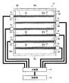
図1は、本発明のプラズマ処理装置の第1の実施形態に係るプラズマCVD装置の構成を示す図である。Hereinafter, a plasma processing apparatus of the present invention will be described in detail based on preferred embodiments shown in the accompanying drawings.
FIG. 1 is a diagram showing a configuration of a plasma CVD apparatus according to the first embodiment of the plasma processing apparatus of the present invention.
本実施形態の図1に示すプラズマCVD装置10(以下、CVD装置10という)は、第1原料ガス(活性種ガス)として、酸素ガスGfを用い、第2原料ガスとして、TEOSガスGsを用いて、ガラス基板またはシリコンウエハ等の基板(処理対象基板)36の表面36aに対してSiO2膜を形成することを例にして説明する。なお、本発明のプラズマ処理装置においては、基板36に形成する膜はSiO2膜に限定されるものではない。The plasma CVD apparatus 10 (hereinafter referred to as a CVD apparatus 10) shown in FIG. 1 of the present embodiment uses an oxygen gas Gf as a first source gas (active species gas) and uses a TEOS gas Gs as a second source gas. An example in which a SiO2 film is formed on the
図1に示すCVD装置10は、制御部12、分配器14、インピーダンス整合器16、および直方体状の反応容器18を有するものである。この制御部12は、後述するようにCVD装置10の各機器を制御するものである。また、反応容器18は、金属製または合金製であり、接地されている。 A
反応容器18の上壁18aには導入口22が形成されている。この導入口22にガス供給管23が接続されている。さらに、ガス供給管23には、第2のガス供給部28が接続されている。
この第2のガス供給部28は、反応容器18内に、例えば、TEOSガスGs(第2原料ガス)を供給するものである。第2のガス供給部28は、例えば、液体のTEOSが充填されるタンク(図示せず)、液体のTEOSを気化する気化部(図示せず)、および気化されたTEOSの流量を調整する流量調整部(図示せず)を備えるものである。この第2のガス供給部28においては、液体のTEOSを気化部により気化してTEOSガスGs(第2原料ガス)を得、流量調整部によりTEOSガスGsの流量が調整されてTEOSガスGsを反応容器18内に供給する。An
The second
また、反応容器18の下壁18bには、排気口24が形成されている。この排気口24に排気管25が接続されている。さらに、排気管25には、真空排気部27が接続されている。この真空排気部27は、ドライポンプおよびターボ分子ポンプなどの真空ポンプを有するものである。また、反応容器18には内部の圧力を測定する圧力センサ(図示せず)が設けられている。 An
また、反応容器18の内部には、下壁18b側から順に、表面34aに載置される基板ステージ34、基板36が設けられ、この基板ステージ34の上方に複数のアンテナ素子32からなるアンテナアレイ(プラズマ生成部)30が設けられ、さらには、アンテナアレイ30の上方に、アンテナアレイ30を覆うようにしてガス放射部40(ガス放射板42)が設けられている。 In addition, a
ここで、図2は、本実施形態のプラズマCVD装置のアンテナアレイを示す模式的平面図である。
図2に示すように、アンテナアレイ30は、複数のアンテナ素子32が、基板ステージ34の表面34aと略平行な平面(図示せず)に対して互いに平行に、複数所定の間隙(間)33を設けて配列されて構成されるものである。このアンテナアレイ30は、ガス放射部40下側(下壁18b側)に設けられている。また、アンテナ素子32は、各側壁18c、18dに対しても所定の間隙33が設けられている。本発明においては、アンテナ素子32と各側壁18c、18dとの間隙33も、各アンテナ素子32の間隙33と同様に扱う。Here, FIG. 2 is a schematic plan view showing an antenna array of the plasma CVD apparatus of the present embodiment.
As shown in FIG. 2, the
また、アンテナアレイ30においては、各アンテナ素子32が、反応容器18の対向する2つの側壁18cおよび側壁18dに亘り配置されている。このアンテナアレイ30(各アンテナ素子32)が、ガス放射部40(図1参照)のガス放射板42(図1参照)及び基板ステージ34の表面34a(図1参照)に対して平行に設けられている。 Further, in the
アンテナ素子32はモノポールアンテナであり、反応容器18の側壁18e、18fに形成した開口部(図示せず)に電気的に絶縁して取り付けられている。
アンテナアレイ30においては、図2に示すように隣接するアンテナ素子32と互いに逆方向に反応容器18内の側壁18e、18fから突出しており、給電方向が逆向きとなっている。これらのアンテナ素子32は、高周波電流供給端の側がインピーダンス整合器16に接続されている。このインピーダンス整合器16はマッチングボックスである。The
As shown in FIG. 2, the
インピーダンス整合器16は、制御部12の高周波電源が発生する高周波信号の周波数の調整とともに用いて、プラズマの生成中にアンテナ素子32の負荷の変化によって生じるインピーダンスの不整合を是正するために用いられるものである。 The
各アンテナ素子32は、電気伝導率の高い導体からなる棒状(パイプであってもよい)を成し、使用する高周波の波長の(2n+1)/4倍(nは0または正の整数である)の長さをモノポールアンテナであるアンテナ素子の放射長さとする。
各アンテナ素子32は、石英等の誘電体からなる円筒部材37に収納されており、各アンテナ素子32の表面は石英等の誘電体で覆われている。このように、棒状の導体を誘電体で覆うことにより、アンテナ素子32としての容量とインダクタンスが調整される。これにより、アンテナ素子32の長手方向に沿って高周波電流を効率よく伝播させることができ、電磁波を効率よく放射させることができる。なお、以下、アンテナ素子32の表面とは、棒状の導体の表面ではなく、円筒部材37の表面37aのことをいう。Each
Each
本実施形態においては、インピーダンス整合器16を設け、さらに後述するように、ガス放射部40(ガス放射板42)に形成された金属膜が接地されていることにより、鏡像関係に形成される電磁波と作用して、アンテナ素子32毎に所定の電磁波を形成する。さらに、アンテナアレイ30を構成するアンテナ素子32は、隣接するアンテナ素子32と給電方向が逆向きとなっているので、反応室39において電磁波は均一に形成される。 In the present embodiment, the
ここで、図1に示すように、基板ステージ34は、上述のように、表面34aに基板36が載置されるものである。この基板ステージ34においては、基板ステージ34の中心と基板36の中心とを一致させて基板36が載置される。
また、基板ステージ34の内部には基板36を加熱する発熱体(図示せず)が設けられており、さらに接地された電極板(図示せず)が設けられている。この発熱体は、制御部12に接続されており、発熱体による加熱は、制御部12に制御される。
なお、電極板がバイアス電源(図示せず)に接続され、このバイアス電源により電極板に所定のバイアス電圧が印加される構成でもよい。Here, as shown in FIG. 1, in the
In addition, a heating element (not shown) for heating the
The electrode plate may be connected to a bias power source (not shown), and a predetermined bias voltage may be applied to the electrode plate by the bias power source.
また、図1に示すように、ガス放射部40は、例えば、SiCからなるガス放射板42に、直径が0.3〜1.0mm程度の貫通穴が複数形成されたものである。これらの貫通穴がガス放出口44となる。また、ガス放射部40においては、ガス放射板42の表面に金属膜が形成されており、接地されている。
本実施形態において、ガス放射部40のガス放射板42は、反応容器18の内部の全域に亘る大きさを有するものであり、アンテナアレイ30を覆うように設けられている。このガス放射部40により、反応容器18内が2つの空間に仕切られており、ガス放射部40の上壁18a側の空間がガス分散室38であり、ガス放射部40の下壁18b側の空間が反応室39である。
このガス放射部40は、ガス分散室38に供給されたガスを広い面積に渡って反応室39内に拡散させるものである。本実施形態においては、ガス放射部40は、第2のガス供給部28から導入されたTEOSガスGsを広い面積に渡って、反応室39内に拡散させるものである。Moreover, as shown in FIG. 1, the gas radiation | emission part 40 is the gas radiation |
In the present embodiment, the
The gas radiating unit 40 diffuses the gas supplied to the
さらには、ガス放射部40においては、ガス放射板42を基板ステージ34の表面34aに垂直な方向から見た場合、下方に設けられたアンテナアレイ30のアンテナ素子32の位置と整合する第1の領域42aに形成された各ガス放射口44と、アンテナ素子32の位置と整合しない領域、すなわち、アンテナ素子32とアンテナ素子32との間(間隙33)の領域に整合する第2の領域42b、およびアンテナ素子32と反応容器18の壁面との間(間隙33)に整合する第2の領域42bの各ガス放射口44とを隔離するための隔壁によって流路46が形成されている。
流路46は、アンテナ素子32と整合する第1の領域42aに形成された全てのガス放射口44に接続(連通)されており、流路46を介して、全てのガス放射口44に、例えば、酸素ガスGf(第1原料ガス)を供給することができる。
この流路46は、断面形状がコ字形状の隔壁部材が、ガス放射板42の表面に、アンテナ素子32が伸びる方向に沿って設けられて形成されたものである。流路46には、第1のガス供給部26が接続されている。Further, in the gas radiating unit 40, when the
The
The
第1のガス供給部26は、例えば、ガスボンベ(図示せず)および流量調整部(図示せず)を備えるものであり、このガスボンベには酸素ガスGfが充填されている。この第1のガス供給部26により、流路46を介して、ガス放射口44から酸素ガスGfがアンテナ素子32の長さ方向の全域に亘って、アンテナ素子32の表面37aの周囲に供給され、さらには、反応室39内に供給される。
また、アンテナ素子32の位置と整合しない第2の領域42bのガス放射口44は、ガス分離室38および反応室39と連通しており、ガス分離室38に供給されたTEOSガスGsを反応室39内に供給するものである。The first
In addition, the
このように、ガス放射部40においては、流路46により、複数のガス放射口44のうち、第1の領域42aに形成されたものについては、第2の領域42bに形成された他のガス放射口44とは隔離されている。このため、第1の領域42aに形成されたガス放射口44からは、第2のガス供給部28から供給されたTEOSガスGsが放出されない。このため、アンテナ素子32の表面37aの周囲には、流路46を介して供給された酸素ガスGfが供給される。よって、ガス放射部40により、アンテナ素子32の表面37aの周囲には、TEOSガスGsが供給されることなく、酸素ガスGfが供給される。
なお、流路46を介して第1のガス供給部26から供給されるガスは、酸素ガスに限定されるものではなく、成膜のために供給されるガスのうち、アンテナ素子32の表面37aに、付着もしくは堆積することがないもの、または付着もしくは堆積する程度が小さいものであればよい。
上述のように、本実施形態のガス放射部40は、酸素ガスGfの供給路を隔離し、TEOSガスGsの供給路を隔離しないものである。As described above, in the gas radiating portion 40, the gas formed in the
Note that the gas supplied from the first
As described above, the gas radiation unit 40 of the present embodiment isolates the supply path of the oxygen gas Gf and does not isolate the supply path of the TEOS gas Gs.
制御部12は、高周波発振回路、増幅器からなる高周波電源(図示せず)および電流・電圧センサ(図示せず)を有し、電流・電圧センサの検知信号に応じて、この高周波電源の発振周波数の変更及びインピーダンス整合器16の調整を行うものである。この制御部12は、アンテナ素子32に共通の高周波信号の周波数を制御して、すべてのアンテナ素子32をインピーダンスが整合した状態に近づけ、この後、各アンテナ素子32に接続されたインピーダンス整合器16によって、各アンテナ素子32のインピーダンスを個別に調整する。制御部12と、複数のインピーダンス整合器16とは、分配器14を介して接続されている。また、制御部12は、アンテナ素子32に高周波信号の給電も制御するものである。 The
なお、制御部12によって、第1のガス供給部26、第2のガス供給部28および真空排気部27も制御されるものである。
この制御部12により、第1のガス供給部26における酸素ガスGf(第1原料ガス)の供給タイミング、および流量などが制御される。また、制御部12により、第2のガス供給部28におけるTEOSガスGsの供給タイミング、および流量などが制御される。さらには、制御部12により、反応容器18内の原料ガス等を排気することができ、さらには反応容器18内の圧力を所望の圧力に調整することができる。The first
The
本実施形態においては、例えば、SiO2膜の成膜時、第1のガス供給部26から導入されたTEOSガスGsが、反応容器18内を上壁18a側から下壁18b側(以下、上壁18a側から下壁18b側に向かう方向を「垂直方向」という)に流れ、排気口24から排出される。なお、後述するように、このTEOSガスGsは、排出までの過程に、反応容器18内において、活性化され、更には励起されて反応活性種とされた酸素ガスGfと混合され、混合ガスとなる。In the present embodiment, for example, when the SiO2 film is formed, the TEOS gas Gs introduced from the first
本実施形態においては、制御部12により、反応容器18内の圧力を真空排気部27により1Pa〜数100Pa程度の状態とし、流路46を介して酸素ガスGf(第1原料ガス)をアンテナ素子32の表面37aの周囲を経て供給し、TEOSガスGsをガス放射板42のガス放射口44から供給する。さらに、アンテナ素子32に高周波信号を給電することにより、アンテナ素子32の周囲に電磁波を放射させる。これにより、反応容器18内のアンテナ素子32の近傍でプラズマ(図示せず)が生成されるとともに、ガス放射部40から放射された酸素ガスGf(活性種ガス)が励起されて酸素ラジカル(反応活性種)が得られる。その際、発生したプラズマは導電性を有するので、アンテナ素子32から放射された電磁波はプラズマで反射され易い。このため、電磁波はアンテナ素子32周辺の局部領域に局在化する。このように、モノポールアンテナからなるアンテナ素子32を複数有するアンテナアレイ30では、プラズマがアンテナ素子32の表面37aの近傍に局在化して形成され、アンテナ素子32の表面37aの周囲では、電界分布が極度に高くなる。 In the present embodiment, the
なお、このようなアンテナアレイを用いたプラズマ生成の原理についての詳細な説明が、本願出願人による先の出願である、特開2003−86581号公報に記載されている。また、アンテナアレイを用いたプラズマ生成装置における、各アンテナ毎の詳細なインピーダンス整合方法が、同じく本願出願人による先の出願である、特願2005−014256号明細書に記載されている。本発明におけるアンテナアレイおよび各アンテナ毎の詳細なインピーダンス整合方法として、例えば、上記各明細書に記載の方法を利用すればよい。 A detailed description of the principle of plasma generation using such an antenna array is described in Japanese Patent Application Laid-Open No. 2003-86581, which is an earlier application by the present applicant. A detailed impedance matching method for each antenna in a plasma generation apparatus using an antenna array is described in Japanese Patent Application No. 2005-014256, which is an earlier application filed by the present applicant. As the antenna array and the detailed impedance matching method for each antenna in the present invention, for example, the methods described in the above specifications may be used.
次に、本実施形態のCVD装置10の成膜方法について、SiO2膜を例にして説明する。
先ず、第1のガス供給部26から酸素ガスGf(活性種ガス)を流路46に一定流量で流入させ、アンテナ素子32の配置位置に整合する第1の領域42aに形成されたガス放射口44から酸素ガスGfを、アンテナ素子32の表面37aの周囲に供給し、酸素ガスGfを反応室39に一定の流速で流入させる。このとき、第2のガス供給部28からガス供給管23を介して、TEOSガスGsをガス分散室38に一定流量で放出し、放射部40の流路46が設けられておらず、ガス分散室38と連通する第2の領域42bに形成されたガス放射口44から反応室39内に一定の流速で流入させる。
なお、酸素ガスGfおよびTEOSガスGsを供給する場合、反応容器18(反応室39)は真空排気部27により排気されており、制御部12により、反応容器18(反応室39)内が、例えば、1Pa〜数100Pa程度の圧力に保持されている。これにより、反応容器18(反応室39)の垂直方向に酸素ガスGfおよびTEOSガスGsが流れる。Next, a film forming method of the
First, an oxygen gas Gf (active species gas) is flowed from the first
When supplying the oxygen gas Gf and the TEOS gas Gs, the reaction vessel 18 (reaction chamber 39) is evacuated by the
次に、アンテナ素子32に高周波信号を給電して、アンテナ素子32の周囲に電磁波を放射させる。これにより、反応室39内で、アンテナ素子32の近傍に局在化したプラズマが生成され、ガス放出口44から放射された酸素ガスGf(活性種ガス)が解離された酸素ラジカル(反応活性種)が得られる。また、TEOSガスが解離されたTEOSラジカル(活性化されたTEOSガス)が得られる。
アンテナアレイ30のアンテナ素子32の周囲近傍で、酸素ラジカル(反応活性種)と、TEOSラジカルとが混合されて混合ガスとなる。活性状態である酸素ラジカル(反応活性種)とTEOSラジカルとが混合されると、活性状態の活性エネルギによって、基板36の表面36aにSiO2膜が形成される。Next, a high frequency signal is fed to the
In the vicinity of the periphery of the
本実施形態においては、放射部40に流路46を形成し、アンテナ素子32の表面37aに酸素ガスGf(第1原料ガス)だけを供給し、TEOSガスGsは、アンテナ素子32の間隙33(間)を通過させて、処理室39に供給する。このようにアンテナ素子32の表面37aには酸素ガスGfしか供給されないため、アンテナアレイ30を用いて、プラズマを生成した場合でも、アンテナ素子32の表面37aには酸素ガスGfだけが存在する。これにより、アンテナ素子32の表面37aに、SiO2などの反応生成物の付着または堆積が抑制される。このように、アンテナ素子32の表面37aにSiO2などの反応生成物が付着または堆積することが抑制されるため、パーティクルの発生が抑制される。さらには、パーティクルの発生が抑制されるため、形成する膜(SiO2膜)の膜質についても優れたものが得られる。
さらには、本実施形態においては、アンテナ素子32の表面37aへのSiO2などの反応生成物の付着が抑制されるため、SiO2膜の成膜に利用される酸素ガスGfおよびTEOSガスGsの割合(利用効率)が増えるため、成膜速度も向上する。
なお、基板36が、例えば、1m×1m程度の大きなものである場合であっても、アンテナアレイ30は、均一なプラズマを生成することができ、上述のようにパーティクルの発生が抑制され、さらには、成膜速度が速いことから、膜質が優れたSiO2膜を従来よりも早く形成することができる。In the present embodiment, the
Furthermore, in this embodiment, since the adhesion of reaction products such as SiO2 to the
Even if the
なお、本実施形態においては、第2のガス供給部28に代えて、原料ガス供給部(図示せず)を設け、第1のガス供給部26に代えて、第3のガス供給部(図示せず)も設ける構成としてもよい。
この場合、原料ガス供給部は、反応容器18内に、基板36の表面36aに形成する膜を得るために必要な原料ガスを供給するためのものである。例えば、基板36の表面36aにSiO2膜を形成する場合には、原料ガスとしては、酸素ガス(第1原料ガス)およびTEOSガス(第2原料ガス)の混合ガスを供給するものである。In the present embodiment, a source gas supply unit (not shown) is provided instead of the second
In this case, the source gas supply unit is for supplying source gas necessary for obtaining a film to be formed on the
原料ガス供給部は、形成する膜に応じたガスの種類および数に応じた分のガスボンベ(図示せず)を備え、このガスボンベからのガスの流量を調整する流量調整部(図示せず)を備えるものである。本実施形態においては、ガスボンベに酸素ガス(第1原料ガス)が充填されている。
また、原料ガス供給部は、TEOSガスGsを供給するために、液体が充填されるタンク(図示せず)、液体を気化する気化部(図示せず)、および気化部により気化された気体の流量を調節する流量調整部(図示せず)を備える。本実施形態においては、タンクに液体のTEOSが充填されており、気化部により気化してTEOSガスGs(第2原料ガス)が得られ、流量調整部によりTEOSガスGsの流量が調整される。
本実施形態においては、原料ガス供給部からガス分離室38に、酸素ガス(第1原料ガス)およびTEOSガス(第2原料ガス)が混合されている原料ガスが供給される。
また、第3のガス供給部は、原料ガス以外、例えば、酸素ガスGfおよびTEOSガスGs以外の成膜に利用されない気体(第3のガス)を供給するためのものである。この第3のガス供給部は、例えば、ガスボンベ(図示せず)および流量調整部(図示せず)を備えるものであり、このガスボンベには、成膜に利用されない気体が充填されている。本実施形態においては、例えば、充填される気体としては、アルゴンガス、窒素ガスなどの不活性ガスである。The raw material gas supply unit includes a gas cylinder (not shown) corresponding to the type and number of gases according to the film to be formed, and a flow rate adjusting unit (not shown) that adjusts the flow rate of the gas from the gas cylinder. It is to be prepared. In this embodiment, the gas cylinder is filled with oxygen gas (first source gas).
The source gas supply unit supplies a TEOS gas Gs with a tank (not shown) filled with a liquid, a vaporization unit (not shown) for vaporizing the liquid, and a gas vaporized by the vaporization unit. A flow rate adjusting unit (not shown) for adjusting the flow rate is provided. In the present embodiment, the tank is filled with liquid TEOS, and is vaporized by the vaporization unit to obtain TEOS gas Gs (second raw material gas). The flow rate adjustment unit adjusts the flow rate of the TEOS gas Gs.
In the present embodiment, a source gas in which oxygen gas (first source gas) and TEOS gas (second source gas) are mixed is supplied from the source gas supply unit to the
The third gas supply unit is for supplying a gas (third gas) that is not used for film formation other than the source gas, for example, oxygen gas Gf and TEOS gas Gs. The third gas supply unit includes, for example, a gas cylinder (not shown) and a flow rate adjustment unit (not shown), and the gas cylinder is filled with a gas that is not used for film formation. In the present embodiment, for example, the gas to be filled is an inert gas such as argon gas or nitrogen gas.
このような構成においては、原料ガス供給部から供給された原料ガスを、アンテナ素子32間の間隙33、およびアンテナ素子32と反応容器18の壁面との間隙33から反応室39内に一定の流速で流入させる。また、第3のガス供給部から、アンテナ素子32の配置位置に整合する第1の領域42aに形成されたガス放射口44から成膜に利用されない気体(第3のガス)を、アンテナ素子32の表面37aの周囲に供給して反応室39内に拡散させる。このように、原料ガス(酸素ガス(第1原料ガス)、およびTEOSガス(第2原料ガス)の混合ガス)および気体(第3のガス)が反応室39内に供給された状態で、アンテナアレイ30を用いてプラズマを生成する。これにより、酸素ラジカルが得られ、TEOSガスが活性化されて、基板36の表面36aにSiO2膜が形成される。In such a configuration, the source gas supplied from the source gas supply unit is supplied at a constant flow rate into the
この場合においては、アンテナ素子32の表面37aの周囲に気体を供給して、アンテナ素子32の表面37aの周囲を原料ガスから隔離しており、アンテナ素子32の表面37aの周囲には、原料ガスが供給されることがない。このため、アンテナ素子32の表面37aに、原料ガスが付着または付着することが抑制される。これにより、パーティクルの発生が抑制され、さらには、成膜速度も向上させることができる。
このように、第2のガス供給部28に代えて、原料ガス供給部(図示せず)を設け、第1のガス供給部26に代えて、第3のガス供給部(図示せず)も設ける構成とした場合においても、膜質が優れた膜を、速い成膜速度で形成することができるという第1の実施形態と同様の効果を得ることができる。In this case, gas is supplied around the
Thus, instead of the second
次に、本発明の第2の実施形態について説明する。
図3は、本発明のプラズマ処理装置の第2の実施形態に係るプラズマCVD装置の構成を示す図である。
なお、本実施形態においては、図1および図2に示す第1の実施形態のプラズマCVD装置と同一構成物には、同一符号を付して、その詳細な説明は省略する。Next, a second embodiment of the present invention will be described.
FIG. 3 is a diagram showing a configuration of a plasma CVD apparatus according to the second embodiment of the plasma processing apparatus of the present invention.
In the present embodiment, the same components as those in the plasma CVD apparatus according to the first embodiment shown in FIGS. 1 and 2 are denoted by the same reference numerals, and detailed description thereof is omitted.
図3に示すように、本実施形態のプラズマCVD装置50は、第1の実施形態のプラズマCVD装置10(図1参照)に比して、第1のガス供給部26および第2のガス供給部28の配置位置、ならびにガス放射部52の構成が異なり、それ以外の構成は、第1の実施例の熱処理装置10と同様の構成であり、その詳細な説明は省略する。 As shown in FIG. 3, the
本実施形態のプラズマCVD装置50においては、第1のガス供給部26がガス供給管23を介して、反応容器18に接続されている。第1のガス供給部26からガス分離室38に酸素ガスGfが供給される。
また、本実施形態のガス放射部52は、第1の実施形態のガス放射部40(図1参照)とは、逆に、酸素ガスGfの供給路を隔離せずに、TEOSガスGsの供給路を隔離するものである。In the
Further, the
本実施形態のガス放射部52は、基本的には、第1の実施形態のガス放射部40(図1参照)と同様の構成であり、例えば、SiCからなるガス放射板54に、直径が0.5mm程度の貫通穴が複数形成されたものである。これらの貫通穴がガス放出口56となる。また、ガス放射部52も、ガス放射板54の表面に金属膜が形成されており、接地されている。
ガス放射部52は、第1のガス供給部26から導入された酸素ガスGfを広い面積に渡って拡散させるものである。
また、本実施形態において、ガス放射部52のガス放射板54も、反応容器18の内部の全域に亘る大きさを有し、アンテナアレイ30を覆うように設けられている。このガス放射部52により、反応容器18内が2つの空間に仕切られている。反応容器18の内において、ガス放射部52の上壁18a側の空間がガス分散室38であり、ガス放射部52の下壁18b側の空間が反応室39である。The
The
In the present embodiment, the
さらには、ガス放射部52においては、ガス放射板54を、基板ステージ34の表面34aに垂直な方向から見た場合、下方に設けられたアンテナ素子32とアンテナ素子32との間(間隙33)と整合する第2の領域54b、およびアンテナ素子32と反応容器18の壁面との間(間隙33)と整合する第2の領域54bに形成された各ガス放射口56を、アンテナ素子32の位置に整合する第1の領域54aに形成されたガス放射口56と隔離するように、アンテナ素子32の伸びる方向に沿ってガス放射板54の表面に、隔壁によって流路58が形成されている。 Further, in the
流路58は、アンテナ素子32とアンテナ素子32との間(間隙33)と整合する第2の領域54b、およびアンテナ素子32と反応容器18の各側壁18c、18dとの間(間隙33)と整合する第2の領域54bに形成された全てのガス放射口56と接続(連通)しており、流路58を介して、全てのガス放射口56に、例えば、TEOSガスGsを供給することができる。
この流路58は、断面形状がコ字形状の隔壁部材が、ガス放射板54の表面に、アンテナ素子32が伸びる方向に沿って設けられて形成されたものである。流路58には、第2のガス供給部28が接続されている。
この第2のガス供給部28により、流路58を介して、ガス放射口56からTEOSガスGsがアンテナ素子32の長さ方向の全域に亘って、アンテナ素子32間の間隙33、およびアンテナ素子32と反応容器18の各側壁18c、18dとの間隙33から、反応室39内に供給される。The
The
The second
ガス放射部52においては、流路58により、複数のガス放射口56のうち、第2の領域54bに形成されたものについては、アンテナ素子32の配置位置と整合する第1の領域54aに形成された他のガス放射口56とは隔離されている。このため、流路58を介して、第2の領域54bに形成されたガス放射口56からは、第2のガス供給部28から供給されたTEOSガスGsが放射される。すなわち、アンテナ素子32の間隙33から、TEOSガスGsが反応室39内に一定の流速で流入する。 In the
一方、ガス放射板52のアンテナ素子32の表面37aの周囲には、第1のガス供給部26からガス分散室38を経て、第1の領域54aに形成されたガス放射口56から、酸素ガスGfが反応室39内に一定の流速で流入する。
このように、ガス放射部50により、アンテナ素子32の表面37aの周囲には、TEOSガスGsが供給されることなく、酸素ガスGfが供給される。
このように、酸素ガスGfおよびTEOSガスが反応室39内に供給された状態で、アンテナアレイ30を用いてプラズマを生成する。これにより、酸素ラジカルが得られ、TEOSガスが活性化されて、基板36の表面36aにSiO2膜が形成される。On the other hand, around the
As described above, the
As described above, plasma is generated using the
本実施形態のプラズマCVD装置50においては、流路58を介して、アンテナ素子32間の間隙33、およびアンテナ素子32と反応容器18の壁面との間隙33からTEOSガスGsを供給している。一方、アンテナ素子32の表面37aの周囲には、ガス放射板52から酸素ガスGfを供給して、アンテナ素子32の表面37aの周囲をTEOSガスGsから隔離している。このため、アンテナ素子32の表面37aに付着または付着することが抑制される。これにより、パーティクルの発生が抑制され、さらには、成膜速度も向上させることができる。このため、膜質が優れた膜を、速い成膜速度で形成することができる。
また、アンテナアレイ30により、均一なプラズマを生成することができるため、基板が、例えば、1m×1m程度の大きなものである場合であっても、例えば、SiO2膜などを、優れた膜質で、かつ速い成膜速度で形成することができる。In the
In addition, since uniform plasma can be generated by the
また、本実施形態のプラズマCVD装置50においては、酸素ガスGfをガス放射部52に供給するため、ガス放射口56にガスの成分の一部が堆積することもない。このため、パーティクルの発生が抑制されるとともに、ガス放射部52のメンテナンスも簡素化できる。 Further, in the
さらに、本実施形態のプラズマCVD装置50による成膜方法においても、TEOSガスGsを、アンテナ素子32の表面37aの周囲から隔離して、TEOSガスGsを供給しているため、アンテナ素子32の表面37aに付着することが抑制され、第1の実施形態と同様の効果を得ることができる。 Furthermore, in the film forming method using the
なお、本実施形態においても、第1の実施形態の如く、第1のガス供給部26に代えて、第3のガス供給部(図示せず)を設け、第2のガス供給部28に代えて、原料ガス供給部(図示せず)を設ける構成としてもよい。この場合、原料ガス供給部および第3のガス供給部の構成は、第1の実施形態と同様である。 In the present embodiment, a third gas supply unit (not shown) is provided instead of the first
このような構成においては、原料ガス供給部から流路58を介してアンテナ素子32間の間隙33、およびアンテナ素子32と反応容器18の壁面との間隙33に位置するガス放射口56から原料ガスを反応室39内に一定の流速で流入させる。また、第3のガス供給部から、アンテナ素子32の配置位置と整合するガス放射口54から成膜に利用されない気体(第3のガス)を、アンテナ素子32の長さ方向の全域に亘って、アンテナ素子32の表面37aに供給し、反応室39内に拡散させる。このように、原料ガス(酸素ガス(第1原料ガス)、およびTEOSガス(第2原料ガス)の混合ガス)および気体(第3のガス)が反応室39内に供給された状態で、アンテナアレイ30を用いてプラズマを生成する。これにより、酸素ラジカルが得られ、TEOSガスが活性化されて、基板36の表面36aにSiO2膜が形成される。In such a configuration, the raw material gas is supplied from the
この場合においては、アンテナ素子32の表面37aの周囲に気体を供給して、アンテナ素子32の表面37aの周囲を原料ガスから隔離しており、アンテナ素子32の表面37aの周囲には、原料ガスが供給されることがない。このため、アンテナ素子32の表面37aに、原料ガスが付着または付着することが抑制される。これにより、パーティクルの発生が抑制され、さらには、成膜速度も向上させることができる。
このように、第2のガス供給部28に代えて、原料ガス供給部(図示せず)を設け、第1のガス供給部26に代えて、第3のガス供給部(図示せず)を設ける構成とした場合においても、膜質が優れた膜を、速い成膜速度で形成することができるという第1の実施形態と同様の効果を得ることができる。In this case, gas is supplied around the
Thus, instead of the second
次に、本発明の第3の実施形態について説明する。
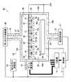
図4は、本発明のプラズマ処理装置の第3の実施形態に係るプラズマCVD装置の構成を示す図である。図5(a)は、本発明のプラズマ処理装置の第3の実施形態に係るプラズマCVD装置の第2原料ガス放出部の一例を示す模式的斜視図であり、(b)は、図5(a)に示す第2原料ガス放出部の第2原料ガス放出部材の模式的断面図であり、(c)は、図5(a)に示す第2原料ガス放出部の第2原料ガス放出部材の他の例を示す模式的断面図である。
なお、本実施形態においては、図1および図2に示す第1の実施形態のプラズマCVD装置と同一構成物には、同一符号を付して、その詳細な説明は省略する。Next, a third embodiment of the present invention will be described.
FIG. 4 is a diagram showing a configuration of a plasma CVD apparatus according to the third embodiment of the plasma processing apparatus of the present invention. FIG. 5A is a schematic perspective view showing an example of the second source gas discharge part of the plasma CVD apparatus according to the third embodiment of the plasma processing apparatus of the present invention, and FIG. It is a typical sectional view of the 2nd source gas discharge member of the 2nd source gas discharge part shown in a), and (c) is the 2nd source gas discharge member of the 2nd source gas discharge part shown in Drawing 5 (a). It is a typical sectional view showing other examples.
In the present embodiment, the same components as those in the plasma CVD apparatus according to the first embodiment shown in FIGS. 1 and 2 are denoted by the same reference numerals, and detailed description thereof is omitted.
図4に示すように、本実施形態のプラズマCVD装置60は、第1の実施形態のプラズマCVD装置10(図1参照)に比して、第1のガス供給部26および第2のガス供給部28の配置位置、ならびにガス放射部62の構成が異なり、更には第2原料ガス放出部70が設けられている点が異なり、それ以外の構成は、第1の実施例の熱処理装置10と同様の構成であり、その詳細な説明は省略する。 As shown in FIG. 4, the
本実施形態のプラズマCVD装置60においては、第1のガス供給部26がガス供給管23を介して、反応容器18に接続されている。第1のガス供給部26からガス分離室38に酸素ガスGfが供給される。
また、本実施形態のガス放射部62は、第1の実施形態のガス放射部40(図1参照)に比して、流路46が形成されていない点が異なり、それ以外の構成は、第1の実施形態のガス放射部40(図1参照)と同様の構成である。
本実施形態においても、ガス放射部62により、反応容器18内が2つの空間に仕切られており、ガス放射部62の上壁18a側の空間がガス分散室38であり、ガス放射部52の下壁18b側の空間が反応室39である。また、本実施形態のガス放射部62も、第1のガス供給部26からガス分離室38に導入された酸素ガスGf(第1原料ガス)を広い面積に渡って反応室39内に拡散させる。In the
Further, the
Also in this embodiment, the inside of the
本実施形態の第2原料ガス放出部70は、酸素ガスGf(第1原料ガス)の流れの途中で、アンテナアレイ30の間隙33に位置するガス放射口から、TEOSガスGs(第2原料ガス)を反応室39内に放出する機能を有するものである。
図5(a)に示すように、この第2原料ガス放出部70は、第2原料ガス放出部材72と、接続管74a、74bと、連結管76とを有し、ガス放射部62の下方に設けられている。The second source
As shown in FIG. 5A, the second source
第2原料ガス放出部材72は、その両端部が折り曲げられた管状の部材からなるものであり、内側に折り曲げられた側とは反対側の周面には、第2原料ガス放出部材72の長手方向に沿って、基板ステージ34の表面34aに対して開口され、所定の大きさを有する穴78(図5(b)参照)が複数形成されている。この穴78が、第2原料ガス放出口である。 The second source
第2原料ガス放出部70においては、第2原料ガス放出部材72が、所定の間隔の間隙73を設けて、例えば、7本並べて配置されている。各隙間73の位置に、アンテナ素子32が配置される。各第2原料ガス放出部材72においては、内側に折り曲げられた部分が、それぞれガス放出板42に形成された穴64に挿通されて、ガス放出板42から上方側に突出している。また、各第2原料ガス放出部材72の端部は、それぞれ接続管74a、74bで接続されている。また、接続管74bには、連結管76が接続されている。一方の連結管76に、第2原料ガスを供給する第2のガス供給部28(図4参照)が接続されている。
また、第2原料ガス放出部70においては、第2原料ガス放出部材72、接続管74a、74bおよび連結管76は、全て連通している。これにより、第2原料ガス放出部70は、第2のガス供給部28からTEOSガスGsが供給されると、各第2原料ガス放出部材72の各穴78からTEOSガスGsが基板ステージ34に向けて噴出される。In the second source
Further, in the second source
また、図5(a)に示すように、第2原料ガス放出部70は、各第2原料ガス放出部材72を穴78が基板ステージ34に向くようにして、アンテナアレイ30の間隙33の位置に来るように反応容器18内に配置されている。この構成により、本実施形態においては、アンテナアレイ30の間隙33、かつガス放射部62によりも基板ステージ34の表面34a(基板36の表面36a)に近い位置から、TEOSガスGsを反応室39に供給することができる。
本実施形態においても、酸素ガスGfおよびTEOSガスが反応室39内に供給された状態で、アンテナアレイ30を用いてプラズマを生成する。これにより、酸素ラジカルが得られ、TEOSガスが活性化されて、基板36の表面36aにSiO2膜が形成される。Further, as shown in FIG. 5A, the second source
Also in the present embodiment, plasma is generated using the
なお、第2原料ガス放出部70において、第2原料ガス放出部材72の穴78は、基板ステージ34の表面34a(基板36の表面36a)に対して、TEOSガスGsが均一に放出されるように形成されていれば、形状および配置パターンについては、特に限定されるものではない。例えば、図5(c)に示すように、第2原料ガス放出部材72aの下方側の周面に、長手方向と直交する管の断面において、穴78a、78bを互いに対向する位置に形成してもよい。 In the second source
本実施形態のプラズマCVD装置60においては、アンテナアレイ30の間隙33に設けた各第2原料ガス放出部72の各穴78からTEOSガスGsを放出するため、アンテナ素子32の表面37aの周囲には、TEOSガスGsが流入しない。また、アンテナ素子32の表面37aの周囲には、ガス放出口から酸素ガスGfが供給される。
このため、酸素ガスGfとTEOSガスGsとが反応して生成されるSiO2がアンテナ素子32の表面37aに付着または堆積することがより一層抑制される。これにより、パーティクルの発生がより一層抑制され、さらには、酸素ガスGfとTEOSガスGsの利用効率も上がるため、成膜速度も向上させることができる。よって、膜質が優れた膜を、速い成膜速度で形成することができる。このように、本実施形態においても、第1の実施形態と同様の効果を得ることができる。In the
For this reason, it is further suppressed that SiO2 produced by the reaction of the oxygen gas Gf and the TEOS gas Gs adheres to or accumulates on the
また、本実施形態のプラズマCVD装置60においては、第2原料ガス放出部70を設け、TEOSガスGsを別供給とし、ガス放射部62よりも基板ステージ34(基板36)に近い位置からTEOSガスGsを供給することにより、基板ステージ34の表面34a全面に向けて均一にTEOSガスGsを放出することができる。これにより、成膜速度の均一性を高めることもできる。
さらに、本実施形態のプラズマCVD装置60においては、酸素ガスGfをガス放射部62に供給するため、ガス放射部62のガスガス放射口66に供給されたガスの成分の一部が堆積することもない。このため、パーティクルの発生が抑制されるとともに、ガス放射部62のメンテナンスも簡素化できる。Further, in the
Furthermore, in the
また、本実施形態のプラズマCVD装置60による成膜方法においても、アンテナ素子32の間隙33に設けられた各第2原料ガス放出部材72の各穴78から、ガス放射部62よりも基板ステージ34に近い位置からTEOSガスGsを放出しているため、アンテナ素子32の表面37aの周囲がTEOSガスGsから隔離されて、酸素ガスGfおよびTEOSガスGsが供給されることになる。また、SiO2(反応生成物)も、アンテナアレイ30よりも基板36側で生成されるため、SiO2がアンテナ素子32の表面37aに付着することがより一層抑制される。これにより、パーティクルの発生がより一層抑制され、さらには、酸素ガスGfおよびTEOSガスGsの利用効率も上がるため、成膜速度も向上させることができる。このように、第1の実施形態と同様に、アンテナ素子32の表面37aに付着することが抑制され、第1の実施形態と同様の効果を得ることができる。Also in the film forming method using the
また、本実施形態においては、基板36の表面36a近傍で、酸素ガスGf(反応活性種ガス)とTEOSガスGsとの均一な混合ガスが生成される。このことから、基板36の表面に、例えば、SiO2膜を均一に形成することができる。すなわち、膜厚均一性に優れたSiO2膜を形成することができる。
また、アンテナアレイ30により、均一なプラズマを生成することができるため、基板が、例えば、1m×1m程度の大きなものである場合であっても、膜厚均一性が優れたSiO2膜を形成することができる。In the present embodiment, a uniform mixed gas of oxygen gas Gf (reactive activated species gas) and TEOS gas Gs is generated near the
Further, since the
なお、本実施形態においても、第1の実施形態の如く、第1のガス供給部26に代えて、原料ガス供給部(図示せず)を設け、第2のガス供給部28に代えて、第3のガス供給部(図示せず)を設ける構成としてもよい。この場合、原料ガス供給部および第3のガス供給部の構成は、第1の実施形態と同様である。 In the present embodiment, as in the first embodiment, instead of the first
このような構成においては、第3のガス供給部により、ガス放射部62のガス放射口44から成膜に利用されない気体(第3のガス)を、アンテナ素子32の長さ方向の全域に亘って、アンテナ素子32の表面37aに供給し、反応室39内に拡散させる。また、原料ガス供給部から、第2原料ガス放出部70を介して供給された原料ガスを反応室39内に一定の流速で流入させる。このように、原料ガス(酸素ガス(第1原料ガス)、およびTEOSガス(第2原料ガス)の混合ガス)および気体(第3のガス)が反応室39内に供給された状態で、アンテナアレイ30を用いてプラズマを生成する。これにより、酸素ラジカルが得られ、TEOSガスが活性化されて、基板36の表面36aにSiO2膜が形成される。In such a configuration, the third gas supply unit causes the gas (third gas) that is not used for film formation to flow from the
この場合においては、アンテナアレイ30の間隙33に設けた各第2原料ガス放出部72の各穴78から、アンテナ素子32間の間隙33から原料ガスを、気体(第3のガス)とは別に供給している。さらに、アンテナ素子32の表面37aの周囲には気体を供給して、アンテナ素子32の表面37aの周囲を原料ガスから隔離しており、アンテナ素子32の表面37aの周囲には、原料ガスが供給されることがない。このため、アンテナ素子32の表面37aに、原料ガスが付着または付着することが抑制される。これにより、パーティクルの発生が抑制され、さらには、成膜速度も向上させることができる。
このように、第2のガス供給部28に代えて、原料ガス供給部(図示せず)を設け、第2原料ガス放出部70から原料ガスを供給する構成とし、第1のガス供給部26に代えて、第3のガス供給部(図示せず)も設ける構成とした場合においても、膜質が優れた膜を、速い成膜速度で形成することができるという第1の実施形態と同様の効果を得ることができる。In this case, the source gas is separated from the
Thus, instead of the second
上述のいずれの実施形態のCVD装置においても、基板36の表面36aにSiO2膜を成膜する装置を例に説明したが、本発明のプラズマ処理装置はこれに限定されるものではない。本発明のプラズマ処理装置は、半導体素子、液晶表示パネルもしくはプラズマディスプレイパネルなどのフラットディスプレイパネル、および太陽電池などにおける各種の膜の成膜に用いることができる。さらに、本発明のプラズマ処理装置は、エッチング装置として用いることもでき、さらにまた、基板ステージのクリーニング処理に用いることもできる。In any of the above-described CVD apparatuses, the apparatus for forming the SiO2 film on the
また、上述のいずれの実施形態のCVD装置においても、プラズマ生成部として、モノポールアンテナが複数配置されたアンテナアレイ30を用いることより、アンテナアレイ30近傍に局在化させてプラズマを生成するものである。この構成により、基板ステージ34に載置された基板36にプラズマが直接曝されない状態で、基板36とアンテナアレイ30との距離を比較的近づけて配置することを可能にしている。これにより、アンテナアレイ30近傍で励起された酸素ラジカル(反応活性種)の励起寿命に対して、アンテナアレイ30と基板36との距離を十分に近づけることを可能としている。すなわち、酸素ラジカル(反応活性種)が十分に励起した状態で基板の表面に到達することを可能としている。 In any of the above-described CVD apparatuses, the plasma generation unit uses the
さらに、上述のいずれのCVD装置においても、基板36の表面36aにSiO2膜を成膜するために、酸素ガスGf(第1原料ガス)およびTEOSガスGs(第2原料ガス)の2種類のガスを用いて説明したが、本発明はこれに限定されるものではない。第1原料ガスおよび第2原料ガスは、形成する膜の種類に応じて、用いられるガスの種類および数は、適宜選択されるものである。なお、第1原料ガスとしては、アンテナ素子32の表面37aに曝した場合、その表面37aに付着物が生じないものであるか、または表面37aの付着量が第2原料ガスによりも少ないものであればよい。Further, in any of the above-described CVD apparatuses, in order to form a SiO2 film on the
さらに、第1原料ガスとしては、酸素ガス以外に、例えば、窒素ガス、水素ガスおよびアルゴンガスを用いることができる。さらに、第2原料ガスとしては、第1原料ガス以外の膜を形成するためのガスが用いられ、例えば、金属化合物を含むガスが用いられる。
なお、例えば、シリコン膜を形成する場合、第1原料ガスとして、水素ガスを用い、第2原料ガスとしては、シランガスを用いる。この場合でも本発明の効果を得ることができる。
さらには、例えば、成膜またはエッチングなどに、2種類のガスを混合して使用する場合、アンテナ素子の表面の周囲には、このアンテナ素子の表面に付着、さらには堆積する成分を含む気体を供給せずに、このような気体をアンテナ素子の間隙から供給すれば、使用されるガスの種類は、特に限定されるものではない。Furthermore, as the first source gas, for example, nitrogen gas, hydrogen gas, and argon gas can be used in addition to oxygen gas. Furthermore, as the second source gas, a gas for forming a film other than the first source gas is used, and for example, a gas containing a metal compound is used.
For example, when forming a silicon film, hydrogen gas is used as the first source gas, and silane gas is used as the second source gas. Even in this case, the effect of the present invention can be obtained.
Furthermore, for example, when two types of gases are mixed and used for film formation or etching, a gas containing a component that adheres to and deposits on the surface of the antenna element is formed around the surface of the antenna element. If such a gas is supplied from the gap between the antenna elements without being supplied, the type of gas used is not particularly limited.
以上、本発明のプラズマ処理装置について詳細に説明したが、本発明は上記実施形態に限定されず、本発明の主旨を逸脱しない範囲において、種々の改良および変更をしてもよいのはもちろんである。 Although the plasma processing apparatus of the present invention has been described in detail above, the present invention is not limited to the above-described embodiment, and various modifications and changes may be made without departing from the spirit of the present invention. is there.
Claims (9)
Translated fromJapanese前記処理対象基板が表面に配置される基板ステージと、
前記基板ステージの上方に設けられ、誘電体で表面が覆われた棒状の導体で構成したアンテナ素子が前記基板ステージの表面と略平行な平面に対して複数所定の間隙をあけて配列されてなるアンテナアレイを用いてプラズマを生成するプラズマ生成部と、
前記プラズマ生成部を覆うように設けられ、前記アンテナアレイの上方に設けられた複数のガス放射口を有するガス放射板を備えるガス放射部と、
前記ガス放射板の複数のガス放射口の一部分から前記基板ステージの表面に向けて放射して前記アンテナ素子の表面を通るように、第1原料ガスを供給する第1のガス供給部と、
前記ガス放射板の複数のガス放射口の他の部分から前記基板ステージの表面に向けて放射して前記アンテナ素子の間隙を通るように、第2原料ガスを供給する第2のガス供給部と、を有し、
前記プラズマ生成部は、前記プラズマ生成部に対して前記第1原料ガスおよび前記第2原料ガスが供給された状態で、前記アンテナアレイを用いてプラズマを生成し、
前記第1原料ガスは、アルゴン、酸素ガス、水素ガスおよび窒素ガスの群の中から選ばれたガスであることを特徴とするプラズマ処理装置。A plasma processing apparatus for processing a substrate to be processed using a first source gas and a second source gas,
A substrate stage on which the substrate to be treated is disposed;
An antenna element, which is provided above the substrate stage and is composed of a rod-shaped conductor whose surface is covered with a dielectric, is arranged with a plurality of predetermined gaps with respect to a plane substantially parallel to the surface of the substrate stage. A plasma generation unit for generating plasma using an antenna array;
A gas radiating unit including a gas radiating plate provided to cover the plasma generating unit and having a plurality of gas radiating ports provided above the antenna array;
A first gas supply unit for supplying a first source gas so as to radiate from a part of a plurality of gas radiation ports of the gas radiation plate toward the surface of the substrate stage and pass through the surface of the antenna element;
A second gas supply unit configured to supply a second source gas so as to radiate toward the surface of the substrate stage from other portions of the gas radiation ports of the gas radiation plate and pass through the gap between the antenna elements; Have
The plasma generation unit generates plasma using the antenna array in a state where the first source gas and the second source gas are supplied to the plasma generation unit,
The plasma processing apparatus, wherein the first source gas isa gas selected from the group consisting of argon, oxygen gas, hydrogen gas and nitrogen gas .
前記第1のガス供給部からの第1原料ガスは、前記流路を通って、前記第1の領域に形成された全てのガス放射口から放射し、これによって、第1原料ガスは前記アンテナ素子の表面を通り、前記基板ステージの表面に向けて供給され、
前記第2のガス供給部からの第2原料ガスは、前記他のガス放射口から放射し、これによって、第2の原料ガスは、前記アンテナ素子の間隙を通り、前記基板ステージの表面に向けて供給される請求項1に記載のプラズマ処理装置。The plurality of gas radiation ports of the gas radiation plate are formed so as to open to the plasma generation unit, and the gas radiation plate of the gas radiation ports is viewed from a direction perpendicular to the surface of the substrate stage. In this case, a partition that forms a flow path is provided so as to be connected to all the gas emission ports formed in the first region that is aligned with the position of the antenna element. All the gas radiating ports formed in the above and other gas radiating ports formed in other areas are isolated,
The first source gas from the first gas supply unit is radiated from all the gas emission ports formed in the first region through the flow path, whereby the first source gas is radiated from the antenna. Supplied through the surface of the element toward the surface of the substrate stage,
The second source gas from the second gas supply unit radiates from the other gas radiating port, whereby the second source gas passes through the gap between the antenna elements and faces the surface of the substrate stage. The plasma processing apparatus according to claim 1 supplied.
前記第1のガス供給部からの第1原料ガスは、前記他のガス放射口から放射し、これによって、第1の原料ガスは、前記アンテナ素子の表面を通り、前記基板ステージの表面に向けて供給され、
前記第2のガス供給部からの第2原料ガスは、前記流路を通って、前記第2の領域に形成された全てのガス放射口から放射し、これによって、第2原料ガスは前記アンテナ素子の間隙を通り、前記基板ステージの表面に向けて供給される請求項1に記載のプラズマ処理装置。The plurality of gas radiation ports of the gas radiation plate are formed so as to open to the plasma generation unit, and the gas radiation plate of the gas radiation ports is viewed from a direction perpendicular to the surface of the substrate stage. In this case, a partition that forms a flow path is provided so as to be connected to all the gas radiation ports formed in the second region that is aligned with the region of the gap between the antenna elements. All gas emission ports formed in this area and other gas emission openings formed in other areas are isolated,
The first source gas from the first gas supply unit radiates from the other gas emission port, whereby the first source gas passes through the surface of the antenna element and faces the surface of the substrate stage. Supplied,
The second source gas from the second gas supply unit radiates from all the gas emission ports formed in the second region through the flow path, whereby the second source gas is supplied to the antenna. The plasma processing apparatus according to claim 1, wherein the plasma processing apparatus is supplied toward a surface of the substrate stage through an element gap.
前記処理対象基板が表面に配置される基板ステージと、
前記基板ステージの上方に設けられ、誘電体で表面が覆われた棒状の導体で構成したアンテナ素子が前記基板ステージの表面と略平行な平面に対して複数所定の間隙をあけて配列されてなるアンテナアレイを備えるプラズマ生成部と、
前記プラズマ生成部を覆うように設けられ、前記アンテナアレイの上方に設けられ、複数のガス放射口を有するガス放射板を備えるガス放射部と、
前記アンテナアレイの配列面上の、前記プラズマ生成部の前記アンテナ素子の各間隙に設けられ、前記基板ステージに面するように開口された穴が複数形成された中空の第2ガス放出部材を複数備える第2ガス放出部と、
前記第1原料ガスを前記ガス放射板から前記基板ステージの表面に向けて供給する第1のガス供給部と、
前記第2原料ガスを、前記第2ガス放出部を通して、前記基板ステージの表面に向けて供給する第2のガス供給部と、を有し、
前記プラズマ生成部は、前記第1原料ガスおよび前記第2原料ガスが供給された状態で、前記アンテナアレイを用いてプラズマを生成し、
前記第1原料ガスは、アルゴン、酸素ガス、水素ガスおよび窒素ガスの群の中から選ばれたガスであることを特徴とするプラズマ処理装置。A plasma processing apparatus for processing a substrate to be processed using a first source gas and a second source gas,
A substrate stage on which the substrate to be treated is disposed;
An antenna element, which is provided above the substrate stage and is composed of a rod-shaped conductor whose surface is covered with a dielectric, is arranged with a plurality of predetermined gaps with respect to a plane substantially parallel to the surface of the substrate stage. A plasma generator comprising an antenna array;
A gas radiating unit including a gas radiating plate provided to cover the plasma generating unit, provided above the antenna array, and having a plurality of gas radiating ports;
A plurality of hollow second gas discharge members provided in therespective gaps of the antenna elements of the plasma generation uniton the array surface of the antenna array and having a plurality of holes opened so as to face the substrate stage A second gas discharge part comprising:
A first gas supply unit for supplying the first source gas from the gas radiation plate toward the surface of the substrate stage;
A second gas supply unit configured to supply the second source gas through the second gas discharge unit toward the surface of the substrate stage;
The plasma generation unit generates plasma using the antenna array in a state where the first source gas and the second source gas are supplied,
The plasma processing apparatus, wherein the first source gas isa gas selected from the group consisting of argon, oxygen gas, hydrogen gas and nitrogen gas .
前記処理対象基板が表面に配置される基板ステージと、
前記基板ステージの上方に設けられ、誘電体で表面が覆われた棒状の導体で構成したアンテナ素子が前記基板ステージの表面と略平行な平面に対して複数所定の間隙をあけて配列されてなるアンテナアレイを用いてプラズマを生成するプラズマ生成部と、
前記プラズマ生成部を覆うように設けられ、前記アンテナアレイの上方に設けられたガス放射板を備えるガス放射部と、
前記ガス放射部から前記基板ステージの表面に向けて第1原料ガス及び第2原料ガスを放射するように、前記第1原料ガス及び前記第2原料ガスを供給する第1のガス供給部と、
前記ガス放射部から前記基板ステージの表面に向けて第3のガスを放射するように、前記第3のガスを供給する第3のガス供給部と、を有し、
前記ガス放射板には、前記プラズマ生成部に対して開口したガス放出口が複数形成され、前記ガス放射板の前記ガス放射口のうち、前記ガス放射板を前記基板ステージの前記表面に垂直な方向から見た場合、前記アンテナ素子の位置と整合する第1の領域に形成された全てのガス放射口に接続されるように、流路を形成する隔壁が設けられ、この隔壁により、前記第1の領域に形成された全てのガス放射口と、これ以外の領域に形成された他のガス放射口とが隔離され、
前記第3のガス供給部からの前記第3のガスは、前記流路を通り、前記第1の領域に形成された全てのガス放射口から放射し、これによって、前記第3のガスは前記アンテナ素子の表面を通り、前記基板ステージの表面に向けて供給され、
前記第1のガス供給部からの前記第1原料ガス及び前記第2原料ガスは、前記他のガス放射口から放射し、これによって、前記第1原料ガス及び前記第2の原料ガスは、前記アンテナ素子の間隙を通り、前記基板ステージの表面に向けて供給され、
前記プラズマ生成部は、前記第1原料ガス、前記第2原料ガスおよび前記第3のガスが供給された状態で、前記アンテナアレイを用いてプラズマを生成するものであることを特徴とするプラズマ処理装置。A plasma processing apparatus for processing a target substrate using a source gas,
A substrate stage on which the substrate to be treated is disposed;
An antenna element, which is provided above the substrate stage and is composed of a rod-shaped conductor whose surface is covered with a dielectric, is arranged with a plurality of predetermined gaps with respect to a plane substantially parallel to the surface of the substrate stage. A plasma generation unit for generating plasma using an antenna array;
A gas radiating unit provided to cover the plasma generating unit and including a gas radiating plate provided above the antenna array;
A first gas supply unit that supplies the first source gas and the second source gas so as to radiate the first source gas and the second source gas from the gas emission unit toward the surface of the substrate stage;
A third gas supply part for supplying the third gas so as to radiate a third gas from the gas emission part toward the surface of the substrate stage;
The gas radiation plate includes a plurality of gas discharge ports that open to the plasma generation unit, and the gas radiation plate of the gas radiation plate is perpendicular to the surface of the substrate stage. When viewed from the direction, a partition that forms a flow path is provided so as to be connected to all the gas radiation ports formed in the first region that matches the position of the antenna element. All the gas emission ports formed in one region and other gas emission ports formed in other regions are isolated,
The third gas from the third gas supply unit passes through the flow path and radiates from all gas emission ports formed in the first region, whereby the third gas is Supplied through the surface of the antenna element toward the surface of the substrate stage,
The first source gas and the second source gas from the first gas supply unit radiate from the other gas emission port, whereby the first source gas and the second source gas are Supplied through the gap between the antenna elements toward the surface of the substrate stage,
The plasma generation unit is configured to generate plasma using the antenna array in a state where the first source gas, the second source gas, and the third gas are supplied. apparatus.
Applications Claiming Priority (3)
| Application Number | Priority Date | Filing Date | Title |
|---|---|---|---|
| JP2007091869 | 2007-03-30 | ||
| JP2007091869 | 2007-03-30 | ||
| PCT/JP2008/055690WO2008123295A1 (en) | 2007-03-30 | 2008-03-26 | Plasma processing apparatus |
Publications (2)
| Publication Number | Publication Date |
|---|---|
| JP4426632B2true JP4426632B2 (en) | 2010-03-03 |
| JPWO2008123295A1 JPWO2008123295A1 (en) | 2010-07-15 |
Family
ID=39830783
Family Applications (1)
| Application Number | Title | Priority Date | Filing Date |
|---|---|---|---|
| JP2008551375AExpired - Fee RelatedJP4426632B2 (en) | 2007-03-30 | 2008-03-26 | Plasma processing equipment |
Country Status (4)
| Country | Link |
|---|---|
| JP (1) | JP4426632B2 (en) |
| KR (1) | KR101076674B1 (en) |
| TW (1) | TW200917910A (en) |
| WO (1) | WO2008123295A1 (en) |
Families Citing this family (6)
| Publication number | Priority date | Publication date | Assignee | Title |
|---|---|---|---|---|
| EP2360716A1 (en)* | 2008-11-20 | 2011-08-24 | Evatech Co., Ltd. | Plasma processing apparatus |
| JP2014096553A (en)* | 2012-10-09 | 2014-05-22 | Tokyo Electron Ltd | Plasma processing method and plasma processing device |
| KR101619899B1 (en) | 2014-07-25 | 2016-05-12 | 인베니아 주식회사 | A plasma generating module and plasma process apparatus comprising the same |
| KR101640092B1 (en) | 2014-07-25 | 2016-07-18 | 인베니아 주식회사 | A plasma generating module and plasma process apparatus comprising the same |
| KR101640094B1 (en) | 2014-08-08 | 2016-07-18 | 인베니아 주식회사 | A plasma generating module for a plasma process apparatus |
| US20210098230A1 (en)* | 2019-09-27 | 2021-04-01 | Applied Materials, Inc. | Monolithic modular high-frequency plasma source |
Family Cites Families (3)
| Publication number | Priority date | Publication date | Assignee | Title |
|---|---|---|---|---|
| JP2969596B2 (en)* | 1989-10-06 | 1999-11-02 | アネルバ株式会社 | CVD equipment |
| JP2000331993A (en)* | 1999-05-19 | 2000-11-30 | Mitsubishi Electric Corp | Plasma processing equipment |
| JP3327391B2 (en) | 1999-09-09 | 2002-09-24 | 日本電気株式会社 | Thin film manufacturing apparatus and manufacturing method |
- 2008
- 2008-03-26WOPCT/JP2008/055690patent/WO2008123295A1/enactiveApplication Filing
- 2008-03-26KRKR1020097018413Apatent/KR101076674B1/ennot_activeExpired - Fee Related
- 2008-03-26JPJP2008551375Apatent/JP4426632B2/ennot_activeExpired - Fee Related
- 2008-03-28TWTW097111418Apatent/TW200917910A/enunknown
Also Published As
| Publication number | Publication date |
|---|---|
| WO2008123295A1 (en) | 2008-10-16 |
| KR101076674B1 (en) | 2011-10-26 |
| TW200917910A (en) | 2009-04-16 |
| JPWO2008123295A1 (en) | 2010-07-15 |
| KR20090117777A (en) | 2009-11-12 |
Similar Documents
| Publication | Publication Date | Title |
|---|---|---|
| CN104060238B (en) | Liner Assembly And Substrate Processing Apparatus Having Same | |
| KR101831576B1 (en) | Plasma processing device | |
| JP6410622B2 (en) | Plasma processing apparatus and film forming method | |
| KR100241171B1 (en) | A plasma enhanced chemical processing reactor and method | |
| JP4273932B2 (en) | Surface wave excitation plasma CVD equipment | |
| US20120247390A1 (en) | Film formation apparatus | |
| US20100024729A1 (en) | Methods and apparatuses for uniform plasma generation and uniform thin film deposition | |
| US20110008550A1 (en) | Atomic layer growing apparatus and thin film forming method | |
| US8607733B2 (en) | Atomic layer deposition apparatus and atomic layer deposition method | |
| JP4426632B2 (en) | Plasma processing equipment | |
| US20090152243A1 (en) | Plasma processing apparatus and method thereof | |
| US12018375B2 (en) | Flim forming method of carbon-containing film by microwave plasma | |
| US7927455B2 (en) | Plasma processing apparatus | |
| JP2007273752A (en) | Plasma processing apparatus and plasma generation apparatus | |
| JP5551635B2 (en) | Thin film forming equipment | |
| JP4554694B2 (en) | Plasma processing equipment | |
| JP2007273773A (en) | Plasma processing apparatus and plasma processing apparatus cleaning method | |
| US20230282459A1 (en) | Batch type substrate processing apparatus | |
| US8931433B2 (en) | Plasma processing apparatus | |
| JP4554712B2 (en) | Plasma processing equipment | |
| JP2007258570A (en) | Plasma processing equipment | |
| JP2008251838A (en) | Plasma processing equipment | |
| JP2012177174A (en) | Thin film deposition apparatus | |
| JPH06295866A (en) | Plasma reactor | |
| JP2007273818A (en) | Plasma processing equipment |
Legal Events
| Date | Code | Title | Description |
|---|---|---|---|
| TRDD | Decision of grant or rejection written | ||
| A01 | Written decision to grant a patent or to grant a registration (utility model) | Free format text:JAPANESE INTERMEDIATE CODE: A01 Effective date:20091208 | |
| A01 | Written decision to grant a patent or to grant a registration (utility model) | Free format text:JAPANESE INTERMEDIATE CODE: A01 | |
| A61 | First payment of annual fees (during grant procedure) | Free format text:JAPANESE INTERMEDIATE CODE: A61 Effective date:20091210 | |
| R150 | Certificate of patent or registration of utility model | Free format text:JAPANESE INTERMEDIATE CODE: R150 | |
| FPAY | Renewal fee payment (event date is renewal date of database) | Free format text:PAYMENT UNTIL: 20121218 Year of fee payment:3 | |
| FPAY | Renewal fee payment (event date is renewal date of database) | Free format text:PAYMENT UNTIL: 20131218 Year of fee payment:4 | |
| FPAY | Renewal fee payment (event date is renewal date of database) | Free format text:PAYMENT UNTIL: 20141218 Year of fee payment:5 | |
| LAPS | Cancellation because of no payment of annual fees |