JP4422464B2 - Connector chip and manufacturing method thereof - Google Patents
Connector chip and manufacturing method thereofDownload PDFInfo
- Publication number
- JP4422464B2 JP4422464B2JP2003383002AJP2003383002AJP4422464B2JP 4422464 B2JP4422464 B2JP 4422464B2JP 2003383002 AJP2003383002 AJP 2003383002AJP 2003383002 AJP2003383002 AJP 2003383002AJP 4422464 B2JP4422464 B2JP 4422464B2
- Authority
- JP
- Japan
- Prior art keywords
- underlayers
- electrodes
- connector chip
- insulating substrate
- connector
- Prior art date
- Legal status (The legal status is an assumption and is not a legal conclusion. Google has not performed a legal analysis and makes no representation as to the accuracy of the status listed.)
- Expired - Fee Related
Links
Images


Classifications
- H—ELECTRICITY
- H05—ELECTRIC TECHNIQUES NOT OTHERWISE PROVIDED FOR
- H05K—PRINTED CIRCUITS; CASINGS OR CONSTRUCTIONAL DETAILS OF ELECTRIC APPARATUS; MANUFACTURE OF ASSEMBLAGES OF ELECTRICAL COMPONENTS
- H05K3/00—Apparatus or processes for manufacturing printed circuits
- H05K3/36—Assembling printed circuits with other printed circuits
- H05K3/368—Assembling printed circuits with other printed circuits parallel to each other
- H—ELECTRICITY
- H01—ELECTRIC ELEMENTS
- H01R—ELECTRICALLY-CONDUCTIVE CONNECTIONS; STRUCTURAL ASSOCIATIONS OF A PLURALITY OF MUTUALLY-INSULATED ELECTRICAL CONNECTING ELEMENTS; COUPLING DEVICES; CURRENT COLLECTORS
- H01R12/00—Structural associations of a plurality of mutually-insulated electrical connecting elements, specially adapted for printed circuits, e.g. printed circuit boards [PCB], flat or ribbon cables, or like generally planar structures, e.g. terminal strips, terminal blocks; Coupling devices specially adapted for printed circuits, flat or ribbon cables, or like generally planar structures; Terminals specially adapted for contact with, or insertion into, printed circuits, flat or ribbon cables, or like generally planar structures
- H01R12/50—Fixed connections
- H01R12/51—Fixed connections for rigid printed circuits or like structures
- H01R12/52—Fixed connections for rigid printed circuits or like structures connecting to other rigid printed circuits or like structures
- H—ELECTRICITY
- H05—ELECTRIC TECHNIQUES NOT OTHERWISE PROVIDED FOR
- H05K—PRINTED CIRCUITS; CASINGS OR CONSTRUCTIONAL DETAILS OF ELECTRIC APPARATUS; MANUFACTURE OF ASSEMBLAGES OF ELECTRICAL COMPONENTS
- H05K2201/00—Indexing scheme relating to printed circuits covered by H05K1/00
- H05K2201/10—Details of components or other objects attached to or integrated in a printed circuit board
- H05K2201/10227—Other objects, e.g. metallic pieces
- H05K2201/10378—Interposers
- H—ELECTRICITY
- H05—ELECTRIC TECHNIQUES NOT OTHERWISE PROVIDED FOR
- H05K—PRINTED CIRCUITS; CASINGS OR CONSTRUCTIONAL DETAILS OF ELECTRIC APPARATUS; MANUFACTURE OF ASSEMBLAGES OF ELECTRICAL COMPONENTS
- H05K3/00—Apparatus or processes for manufacturing printed circuits
- H05K3/30—Assembling printed circuits with electric components, e.g. with resistor
- H05K3/32—Assembling printed circuits with electric components, e.g. with resistor electrically connecting electric components or wires to printed circuits
- H05K3/34—Assembling printed circuits with electric components, e.g. with resistor electrically connecting electric components or wires to printed circuits by soldering
- H05K3/341—Surface mounted components
- H05K3/3431—Leadless components
- H05K3/3442—Leadless components having edge contacts, e.g. leadless chip capacitors, chip carriers
- Y—GENERAL TAGGING OF NEW TECHNOLOGICAL DEVELOPMENTS; GENERAL TAGGING OF CROSS-SECTIONAL TECHNOLOGIES SPANNING OVER SEVERAL SECTIONS OF THE IPC; TECHNICAL SUBJECTS COVERED BY FORMER USPC CROSS-REFERENCE ART COLLECTIONS [XRACs] AND DIGESTS
- Y10—TECHNICAL SUBJECTS COVERED BY FORMER USPC
- Y10T—TECHNICAL SUBJECTS COVERED BY FORMER US CLASSIFICATION
- Y10T29/00—Metal working
- Y10T29/49—Method of mechanical manufacture
- Y10T29/49002—Electrical device making
- Y10T29/49117—Conductor or circuit manufacturing
- Y10T29/49124—On flat or curved insulated base, e.g., printed circuit, etc.
- Y10T29/49126—Assembling bases
Landscapes
- Engineering & Computer Science (AREA)
- Manufacturing & Machinery (AREA)
- Microelectronics & Electronic Packaging (AREA)
- Coupling Device And Connection With Printed Circuit (AREA)
- Manufacturing Of Electrical Connectors (AREA)
- Multi-Conductor Connections (AREA)
- Road Signs Or Road Markings (AREA)
- Road Paving Structures (AREA)
Description
Translated fromJapanese本発明は、2つの回路基板の各複数の電極の対応する電極をそれぞれ電気的に接続するコネクタチップ及びその製造方法に関するものである。 The present invention relates to a connector chip that electrically connects corresponding electrodes of a plurality of electrodes of two circuit boards, respectively, and a manufacturing method thereof.
特開2000−77556号公報等には、第1の回路基板の表面上に形成された複数の電極と、半導体装置に備えられた第2の回路基板の複数の電極とを複数の球形のボール(BGAボール)からなるコネクタチップを用いて接続する態様が示されている。BGAボールは、少なくとも表面が導電性を有しており、半導体装置に備えられた第2の回路基板の複数の電極にそれぞれ固定されている。そして、複数のBGAボールを備えた半導体装置を第1の回路基板上の所定位置に配置して、複数のBGAボールを第1の回路基板の対応する複数の電極にそれぞれ半田付けする。BGAボールは、球形を有しているので、半田付けする際に、BGAボールの球面と電極の平坦面との間隙に半田が十分に入り込む。そのため、該間隙から半田がはみ出して、フィレットができるのを防ぐことができる。その結果、複数の電極の隣接する電極間の半田による短絡を防止できる。
しかしながら、BGAボールは、球形を有しているため転動しやすく、取り扱いが困難であった。また、BGAボールを半導体装置等に取り付けるには、専用の実装機が必要であった。 However, since the BGA ball has a spherical shape, it is easy to roll and difficult to handle. In addition, a dedicated mounting machine is required to attach the BGA ball to a semiconductor device or the like.
本発明の目的は、 隣接する電極間の短絡防止を図ることができ、しかも専用の実装機等を用いることなく容易に第1の回路基板の複数の電極と第2の回路基板の複数の電極とを接続できるコネクタチップ及びその製造方法を提供することにある。 An object of the present invention is to prevent a short circuit between adjacent electrodes, and easily use a plurality of electrodes on a first circuit board and a plurality of electrodes on a second circuit board without using a dedicated mounting machine or the like. It is to provide a connector chip and a method for manufacturing the same.
本発明の他の目的は、一つのコネクタチップまたは少ない数のコネクタチップで第1の回路基板の複数の電極と第2の回路基板の複数の電極との接続が行えるコネクタチップ及びその製造方法を提供することにある。 Another object of the present invention is to provide a connector chip capable of connecting a plurality of electrodes of a first circuit board and a plurality of electrodes of a second circuit board with a single connector chip or a small number of connector chips, and a method for manufacturing the same. It is to provide.
本発明のコネクタチップは、直方体状の絶縁性基体の6面のうち連続する4つの面上に連続する導電路が形成されており、残りの対向する2つの面上には導電路が形成されていない。本発明のコネクタチップは、導電路が形成されていない2つの面を隣接するコネクタチップと対向させた状態で、導電路が形成された一対の対向面を第1の回路基板の電極と第2の回路基板の電極とにそれぞれ半田付けして、第1の回路基板の電極と第2の回路基板の電極とを接続する。本発明のコネクタチップは、直方体状の形状を有しているので、従来のように転動することがない。そのため、専用の実装機等を用いることなく、容易に第1の回路基板の複数の電極と第2の回路基板の複数の電極とを接続できる。また、コネクタチップの導電路が形成されていない2つの面は、半田が付着し難いので、隣接するコネクタチップの相互の対向面に沿って半田が延びるのを防ぐことができる。そのため、複数の電極の隣接する電極間の半田による短絡を防止できる。 In the connector chip of the present invention, continuous conductive paths are formed on four continuous surfaces of the six surfaces of the rectangular parallelepiped insulating substrate, and conductive paths are formed on the remaining two opposing surfaces. Not. The connector chip of the present invention has a pair of opposing surfaces on which the conductive paths are formed and the electrodes of the first circuit board and the second in a state where the two surfaces on which the conductive paths are not formed are opposed to the adjacent connector chip. The first circuit board electrode and the second circuit board electrode are connected by soldering to the respective circuit board electrodes. Since the connector chip of the present invention has a rectangular parallelepiped shape, it does not roll as in the prior art. Therefore, a plurality of electrodes on the first circuit board and a plurality of electrodes on the second circuit board can be easily connected without using a dedicated mounting machine or the like. In addition, since the two surfaces of the connector chip where the conductive paths are not formed are difficult to be soldered, it is possible to prevent the solder from extending along the mutually facing surfaces of the adjacent connector chips. Therefore, it is possible to prevent a short circuit due to soldering between adjacent electrodes of the plurality of electrodes.
本発明のコネクタチップを用いた回路装置は、第1の回路基板の表面上に形成された複数の電極と、第1の回路基板の上に所定の間隔を開けて配置される第2の回路基板の裏面上に形成された複数の電極とが、導電路を備えた複数のコネクタチップを介して電気的に接続され、導電路と電極とが半田付けにより接続され、複数のコネクタチップにより間隔が維持されている。そして、コネクタチップは、直方体状の絶縁性基体の6面のうち連続する4つの面上に連続する導電路が形成されており、残りの対向する2つの面上には導電路が形成されていない。なお、ここでいう第1及び第2の回路基板は、単体の回路基板でもよいし、電子部品等に備えられた回路基板であってもよい。前述したように本発明のコネクタチップは、専用の実装機等を用いることなく、容易に実装することができるので、本発明のコネクタチップを用いた回路装置は、容易且つ安価に製造することができる。 The circuit device using the connector chip of the present invention includes a plurality of electrodes formed on the surface of the first circuit board, and a second circuit arranged on the first circuit board with a predetermined interval. A plurality of electrodes formed on the back surface of the substrate are electrically connected via a plurality of connector chips provided with conductive paths, and the conductive paths and the electrodes are connected by soldering, and are separated by a plurality of connector chips. Is maintained. In the connector chip, conductive paths are formed on four consecutive surfaces of the six surfaces of the rectangular parallelepiped insulating base, and conductive paths are formed on the remaining two opposing surfaces. Absent. The first and second circuit boards referred to here may be a single circuit board or a circuit board provided in an electronic component or the like. As described above, since the connector chip of the present invention can be easily mounted without using a dedicated mounting machine or the like, the circuit device using the connector chip of the present invention can be easily and inexpensively manufactured. it can.
しかしながら、このようなコネクタチップは、第1の回路基板の複数の電極の内の一つの電極と第2の回路基板の複数の電極の内の一つの電極とを接続するものであるため、接続には多数のコネクタチップを使用しなけらばならない。そこで、本発明の他のコネクタチップは、直方体状の絶縁性基体の6面のうち連続する4つの面から構成される外周面上に、残りの2面が対向する方向に所定の間隔を開けて外周面上を一周する複数の導電路を形成する。このようにいわゆる多連化したコネクタチップでは、一つのコネクタチップに複数の導電路が形成されているため、一つのコネクタチップまたは少ない数のコネクタチップで第1の回路基板の複数の電極と第2の回路基板の複数の電極との接続が行える。そのため、低コストで接続が行える。 However, such a connector chip connects one electrode of the plurality of electrodes of the first circuit board and one electrode of the plurality of electrodes of the second circuit board. A large number of connector chips must be used. Therefore, another connector chip of the present invention has a predetermined interval on the outer peripheral surface constituted by four continuous surfaces of the six surfaces of the rectangular parallelepiped insulating base in the direction in which the remaining two surfaces face each other. Thus, a plurality of conductive paths that make a round on the outer peripheral surface are formed. In such a so-called multiple connector chip, since a plurality of conductive paths are formed in one connector chip, a plurality of electrodes and first electrodes of the first circuit board can be formed with one connector chip or a small number of connector chips. Connection with a plurality of electrodes of the second circuit board can be performed. Therefore, connection can be performed at low cost.
4つの面のうち対向する少なくとも一対の面上には、一対の面上にそれぞれ位置する複数の導電路の部分のうち隣接する2つの導電路の部分間に溶融半田をはじく性質を有する絶縁層をそれぞれ形成するのが好ましい。このようにすれば、複数の導電路を複数の電極にそれぞれ半田付けする際に、複数の導電路と複数の電極との間からはみ出た半田が、絶縁層によって、絶縁基体の隣接する2つの導電路の部分間の表面を伝って延びるのを防ぐことができる。そのため、隣接する2つの電極間で短絡が発生するのを防ぐことができる。 An insulating layer having a property of repelling molten solder between two adjacent conductive path portions among a plurality of conductive path portions respectively positioned on the pair of surfaces on at least a pair of opposing surfaces of the four surfaces Are preferably formed. In this way, when the plurality of conductive paths are soldered to the plurality of electrodes, the solder protruding from between the plurality of conductive paths and the plurality of electrodes is separated by the insulating layer between the two adjacent insulating bases. It can prevent extending along the surface between the portions of the conductive path. Therefore, it is possible to prevent a short circuit from occurring between two adjacent electrodes.
一対の面の一方の面上に形成された絶縁層と他方の面上に形成された絶縁層とは、異なる色を付けるのが好ましい。このようにすれば、コネクタチップを回路基板上に配置する際に、必要に応じてコネクタチップの配置の表裏を判別することができる。 The insulating layer formed on one surface of the pair of surfaces and the insulating layer formed on the other surface are preferably colored differently. In this way, when the connector chip is arranged on the circuit board, the front and back of the arrangement of the connector chip can be discriminated as necessary.
絶縁性基体は、導電路が形成されている複数の導電路形成部分と、導電路が形成されていない複数の非導電路形成部分とが中心線を共有するように中心線に沿って交互に並ぶように形成し、導電路形成部分の中心線と直交する幅寸法を非導電路形成部分の幅寸法よりも小さくするのが好ましい。このようにすれば、導電路は、連続する絶縁基体の4つの面の一方の対向する2つの面上の部分が絶縁性基体の表面に露出し、他方の対向する2つの面上の部分が非導電路形成部分に囲まれた凹部内に形成されることになる。そのため、導電路の一方の対向する2つの面上の部分を第1及び第2の回路基板の電極にそれぞれ接続すれば、半田付けの際に、複数の導電路と第1及び第2の回路基板の複数の電極との間からはみ出た半田が、非導電路形成部分に囲まれた凹部内に入り込む。そのため、このようにはみ出た半田により短絡が発生するのを防ぐことができる。 The insulating substrate is alternately arranged along the center line so that the plurality of conductive path forming portions where the conductive paths are formed and the plurality of non-conductive path forming portions where the conductive paths are not formed share the center line. It is preferable that the width dimension perpendicular to the center line of the conductive path forming portion is smaller than the width dimension of the non-conductive path forming portion. In this way, the conductive path is such that a portion on one of the two opposing surfaces of the four surfaces of the continuous insulating base is exposed on the surface of the insulating base and a portion on the other two opposing surfaces is exposed. It is formed in a recess surrounded by a non-conductive path forming portion. Therefore, if the portions on the two opposing surfaces of the conductive path are respectively connected to the electrodes of the first and second circuit boards, the plurality of conductive paths and the first and second circuits are connected during soldering. Solder that protrudes from between the plurality of electrodes of the substrate enters the recess surrounded by the non-conductive path forming portion. Therefore, it is possible to prevent a short circuit from occurring due to the solder that protrudes in this way.
また、導電路形成部分の中心線と直交する幅寸法を非導電路形成部分の幅寸法よりも大きくすることもできる。このようにすれば、隣接する導電路の間に凹部が形成されることになる。そのため、第1及び第2の回路基板にそれぞれ凹部の開口部が対向するように、コネクタチップを配置して、導電路を第1及び第2の回路基板の電極にそれぞれ接続すれば、半田付けの際に、複数の導電路と第1及び第2の回路基板の複数の電極との間からはみ出た半田が凹部内に入り込む。そのため、このようにはみ出た半田により短絡が発生するのを抑制できる。 Further, the width dimension orthogonal to the center line of the conductive path forming portion can be made larger than the width dimension of the non-conductive path forming portion. In this way, a recess is formed between adjacent conductive paths. Therefore, if the connector chip is arranged so that the opening portions of the recesses face the first and second circuit boards and the conductive paths are connected to the electrodes of the first and second circuit boards, respectively, soldering is performed. At this time, the solder protruding from between the plurality of conductive paths and the plurality of electrodes of the first and second circuit boards enters the recess. Therefore, it is possible to suppress the occurrence of a short circuit due to the solder protruding in this way.
導電路は、一層から構成することもできるが、金属厚膜または金属薄膜からなる下地層の上に1以上のめっき層が形成して構成することもできる。このようにすれば、めっき層の材質を適宜に選択することにより、導電路の耐食性や半田付け性を向上させることができる。 The conductive path can be formed from a single layer, but can also be formed by forming one or more plating layers on a base layer made of a thick metal film or a thin metal film. If it does in this way, the corrosion resistance of a conductive path and solderability can be improved by selecting the material of a plating layer suitably.
下地層は、Ag若しくはCuの金属厚膜またはNi−Cr合金若しくはCuの金属薄膜から構成し、1以上のめっき層は、CuまたはNiからなる第1のめっき層と、第1のめっき層上に形成されてSn合金またはSnからなる第2のめっき層とから構成することができる。このようにすれば、第1のめっき層により耐食性を向上させ、第2のめっき層により半田付け性を向上させることができる。特にSn合金またはSnから第2のめっき層を形成するので、鉛フリーの半田を用いることができ、鉛による環境汚染を防止できる。 The underlayer is composed of a thick Ag or Cu metal film or a Ni-Cr alloy or Cu metal thin film, and the one or more plating layers are a first plating layer made of Cu or Ni, and a first plating layer. And a second plating layer made of Sn alloy or Sn. If it does in this way, corrosion resistance can be improved by the 1st plating layer, and solderability can be improved by the 2nd plating layer. In particular, since the second plating layer is formed from Sn alloy or Sn, lead-free solder can be used, and environmental contamination due to lead can be prevented.
前述した導電路形成部分の中心線と直交する幅寸法が非導電路形成部分の幅寸法よりも小さいコネクタチップは、次のようにして製造することができる。まず、一定の間隔をあけて貫通孔が並んで形成された貫通孔列が複数列並んで設けられた板状の絶縁基板材料を用意する。次に、隣接する2つの貫通孔列の間に位置する2つの貫通孔間に金属厚膜または金属薄膜からなる複数の第1の下地層及び複数の第2の下地層を絶縁基板材料の両面にそれぞれ形成し、複数の第1の下地層の隣接する2つの第1の下地層の間及び複数の第2の下地層の隣接する2つの第2の下地層の間に絶縁層をそれぞれ形成する。そして、複数の第1の下地層の一方の縁部と貫通孔の内面上と複数の第2の下地層の一方の縁部とにそれぞれ亘って金属蒸着により第3の下地層を形成し、複数の第1の下地層の他方の縁部と貫通孔の内面上と複数の第2の下地層の他方の縁部とにそれぞれ亘って金属蒸着により第4の下地層を形成する。次に、貫通孔列のほぼ中央に沿って絶縁基板材料を切断してから、第1〜第4の下地層上に1以上のめっき層を形成する。このようにしてコネクタチップを製造すれば、貫通孔列のほぼ中央に沿って絶縁基板材料を切断することにより、複数の貫通孔が分割されて複数の凹部が形成される。そのため、複数の凹部が形成されたコネクタチップを容易に量産することができる。このような切断は、例えば、貫通孔列のほぼ中央に沿ってブレイク用スリットからなる溝を形成して、このスリットブレイク用スリットに沿って切断することができる。 The connector chip in which the width dimension orthogonal to the center line of the conductive path forming portion is smaller than the width dimension of the non-conductive path forming portion can be manufactured as follows. First, a plate-shaped insulating substrate material is prepared in which a plurality of through-hole rows each having a plurality of through-hole rows arranged with a predetermined interval are arranged. Next, a plurality of first underlayers and a plurality of second underlayers made of a metal thick film or a metal thin film are provided on both sides of the insulating substrate material between two through holes located between two adjacent through hole rows. And forming an insulating layer between two adjacent first underlayers of the plurality of first underlayers and between two adjacent second underlayers of the plurality of second underlayers. To do. Then, a third underlayer is formed by metal deposition over one edge of the plurality of first underlayers, on the inner surface of the through-hole, and one edge of the plurality of second underlayers, A fourth underlayer is formed by metal vapor deposition over the other edge of the plurality of first underlayers, the inner surface of the through hole, and the other edge of the plurality of second underlayers. Next, after cutting the insulating substrate material along substantially the center of the through hole row, one or more plating layers are formed on the first to fourth underlayers. When the connector chip is manufactured in this manner, the plurality of through holes are divided to form a plurality of recesses by cutting the insulating substrate material along substantially the center of the through hole row. Therefore, it is possible to easily mass-produce connector chips in which a plurality of recesses are formed. Such cutting can be performed, for example, by forming a groove composed of a slit for break along substantially the center of the through hole row and cutting along the slit for slit.
絶縁基板材料の片面だけにブレイク用スリットを形成する場合には、絶縁基板材料の両面のそれぞれには、異なる色の絶縁層を形成するのが好ましい。このようにすれば、絶縁層の色によってブレイク用スリットが形成された面を容易に判別することができる。 When the break slits are formed only on one side of the insulating substrate material, it is preferable to form insulating layers of different colors on both sides of the insulating substrate material. In this way, the surface on which the break slit is formed can be easily identified by the color of the insulating layer.
本発明のコネクタチップは、直方体状の形状を有しているので、従来のように転動することがない。そのため、専用の実装機等を用いることなく、容易に第1の回路基板の複数の電極と第2の回路基板の複数の電極とを接続できる。また、コネクタチップの導電路が形成されていない2つの面は、半田が付着し難いので、隣接するコネクタチップの相互の対向面に沿って半田が延びるのを防ぐことができる。そのため、複数の電極の隣接する電極間の半田による短絡を防止できる。 Since the connector chip of the present invention has a rectangular parallelepiped shape, it does not roll as in the prior art. Therefore, a plurality of electrodes on the first circuit board and a plurality of electrodes on the second circuit board can be easily connected without using a dedicated mounting machine or the like. In addition, since the two surfaces of the connector chip where the conductive paths are not formed are difficult to be soldered, it is possible to prevent the solder from extending along the mutually facing surfaces of the adjacent connector chips. Therefore, it is possible to prevent a short circuit due to soldering between adjacent electrodes of the plurality of electrodes.
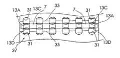
以下、図面を参照して本発明を実施するための最良の形態を詳細に説明する。図1は、本発明の第1の実施の形態のコネクタチップの斜視図であり、図2は、図1のII−II線断面を概略的に表した図である。両図に示すように、本例のコネクタチップ1は、絶縁基体3の表面に6つの導電路5及び14個の絶縁層7が形成されて構成されている。絶縁基体3は、アルミナを96重量%含有するセラミックスにより形成されており、中心線Cを中心に延びる横断面が矩形の細長い形状を呈している。これにより、絶縁基体3は、大まかに言って第1〜第6の面9A〜9Fを有している。絶縁基体3の対向する第3の面9C及び第4の面9Dには、所定の間隔を隔てて横断面がコの字型の溝状の凹部11が6個ずつ並んで形成されている。絶縁基体3の両側にそれぞれ形成された6個の凹部11は、互いに対向する位置に形成されている。このため、本例においては、第3の面9C及び第4の面9Dは、凹凸面となっている。 The best mode for carrying out the present invention will be described below in detail with reference to the drawings. FIG. 1 is a perspective view of a connector chip according to a first embodiment of the present invention, and FIG. 2 is a diagram schematically showing a cross section taken along line II-II in FIG. As shown in both drawings, the
6つの導電路5は、連続する4つの第1〜第4の面9A〜9Dから構成される外周面上に、残りの2面となる第5及び第6の面9E,9Fが対向する方向に所定の間隔を開けて凹部11が形成された位置において外周面上を一周するようにそれぞれ形成されている。言い換えるならば、絶縁性基体3は、導電路5が形成されている複数の導電路形成部分3Aと、導電路5が形成されていない複数の非導電路形成部分3Bとが中心線Cを共有するように中心線Cに沿って交互に並ぶように形成されており、導電路形成部分3Aの中心線Cと直交する幅寸法(矢印Aの方向の寸法)が非導電路形成部分3Bの幅寸法よりも小さく形成されている。図2に示すように、導電路5は、下地層13と、下地層13上に形成された第1のめっき層15Aと、第1のめっき層15A上に形成された第2のめっき層15Bとから構成されている。下地層13は、第1の面9A上に形成された第1の下地層13Aと、第2の面9B上に形成された第2の下地層13Bと、第3の面9C上に形成されて第1の下地層13A及び第2の下地層13Bのそれぞれの一方の縁部を覆う第3の下地層13Cと、第4の面9D上に形成されて第1の下地層13A及び第2の下地層13Bのそれぞれの他方の縁部を覆う第4の下地層13Dとを含んでいる。本例では、第1の下地層13A及び第2の下地層13Bをガラス−Agペーストを用いた金属厚膜により形成し、第3の下地層13C及び第4の下地層13DをNi−Cr合金若しくはCuの金属薄膜により形成している。そして、第1のめっき層15AをCuまたはNiにより形成し、第2のめっき層15BをSn合金またはSnにより形成している。また、このような構成により、導電路5は、第1の面9A上に形成された第1の導電部分5Aと、第2の面9B上に形成された第2の導電部分5Bと、第3の面9C上に形成された第3の導電部分5Cと、第4の面9D上に形成された第4の導電部分5Dとを有することになる。 The six
絶縁層7は、溶融半田をはじく性質を有する材質により形成されており、本例では、エポキシ樹脂またはガラスにより形成されている。この絶縁層7は、絶縁基体3の非導電路形成部分3Bの第1の面9A上及び第2の面9B上にそれぞれ7つずつ形成されている。なお、図1においては、第1の面9A上の絶縁層7しか図示されていないが、第1の面9Aの裏面の第2の面9B上にも絶縁層7は形成されている。絶縁層7は、矩形状を有しており、中心線Cと直交する幅寸法(矢印Aの方向の寸法)が導電路5の第1の導電部分5Aの幅寸法よりわずかに小さくなっている。本例では、第1の面9A上に形成された絶縁層7と第2の面9B上に形成された絶縁層7とは、それぞれ黒色と白色の異なる色を有している。このような色付けは、絶縁層7を形成するエポキシ樹脂またはガラス中に色素を添加することにより行うことができる。 The insulating
図3は、本例のコネクタチップ1を用いた回路装置を正面から見た部分図である。本回路装置は、第1の回路基板21と第2の回路基板23とコネクタチップ1とから構成されている。第1の回路基板21は、絶縁基板22の表面上に複数の電極25が形成されて構成されている。第2の回路基板23は、絶縁基板27の裏面上に複数の電極29が形成されて構成されている。なお、第1及び第2の回路基板21,23は単体の回路基板であってもよいし、電子部品等に備えられた回路基板であっても構わない。第1の回路基板21の複数の電極25と第2の回路基板23の複数の電極29とは、コネクタチップ1の導電路5の第2の導電部分5B及び第1の導電部分5Aにそれぞれ半田付けにより接続されている。これにより、複数の電極25と複数の電極29とは、コネクタチップ1を介して電気的に接続され、第2の回路基板23の複数の電極29は、コネクタチップ1により第1の回路基板21の上に所定の間隔を開けて配置される。 FIG. 3 is a partial view of a circuit device using the
本例のコネクタチップ1を用いれば、複数の導電路5を複数の電極25,29にそれぞれ半田付けする際に、複数の導電路5と複数の電極25,29との間からはみ出た半田が、絶縁層7によって、絶縁基体3の隣接する2つの導電路5,5の部分間の表面(絶縁層7の表面)を伝って延びるのを防ぐことができる。そのため、隣接する2つの電極間(25,25または29,29)で短絡が発生するのを防ぐことができる。また、複数の導電路5と複数の電極25,29との間からはみ出た半田の一部は、凹部11内に入り込む。これによっても半田による短絡を防ぐことができる。 When the
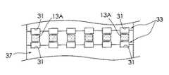
次に、図4A〜図4Eを参照して本例のコネクタチップ1の製造方法について説明する。なお、理解を容易にするため、図4A〜図4Eでは、各工程において形成された部分を点々で表示している。まず、図4Aに示すように、一定の間隔をあけて6つの貫通孔31が並んで形成された複数列の貫通孔列33と、複数列の貫通孔列33のほぼ中央に沿って両面にそれぞれ位置する複数の切断用溝(ブレイク用スリット)35とが形成された板状の絶縁基板材料37を用意する。次に、図4Bに示すように、隣接する2つの貫通孔列33,33の間に位置する2つの貫通孔31,31間にガラス−銀ペーストを用いて金属厚膜からなる複数の第1の下地層13A及び複数の第2の下地層13Bを絶縁基板材料37の両面にそれぞれ形成する。なお、図4A〜図4Eは、いずれも表面側から見た平面図であるため、第1の下地層13Aしか描かれていないが、裏面側には第2の下地層13Bが形成されている。次に、図4Cに示すように、複数の第1の下地層13Aの隣接する2つの第1の下地層13A,13Aの間及び複数の第2の下地層13Bの隣接する2つの第2の下地層13B,13Bの間にエポキシ樹脂またはガラスを塗布して絶縁層7をそれぞれ形成する。次に、図4Dに示すように、複数の第1の下地層13Aの一方の縁部と貫通孔33の内面上と複数の第2の下地層13Bの一方の縁部とに亘ってNi−Cr合金若しくはCuからなる金属蒸着を施して第3の下地層13Cをそれぞれ形成し、複数の第1の下地層13Aの他方の縁部と貫通孔33の内面上と複数の第2の下地層13Bの他方の縁部とに亘ってNi−Cr合金若しくはCuからなる金属蒸着を施して第4の下地層13Dを金属蒸着によりそれぞれ形成する。そして、複数のブレイク用スリット35に沿って絶縁基板材料27を切断する。これにより貫通孔31が分割されて凹部11が形成される。次に、図4Eに示すように、第1〜第4の下地層13A〜13D上にCuまたはNiからなる第1のめっき層15Aを形成してから第1のめっき層15A上にSn合金またはSnからなる第2のめっき層15Bを形成してコネクタチップ1を完成した。 Next, a method for manufacturing the
なお、上記製造例では、絶縁基板材料37を形成する際に複数列の貫通孔列33を絶縁基板材料の成形と一緒に形成したが、絶縁基板材料をガラス−エポキシ樹脂により形成する場合には、板状の絶縁基板材料を形成した後に、パンチングにより、複数列の貫通孔列を形成し、絶縁基板材料の片面にブレイク用スリットを形成することになる。この場合、前述のように第1の面9A上に形成された絶縁層7と第2の面9B上に形成された絶縁層7とが異なる色を有していると、絶縁層の色によって、コネクタチップ製造中にブレイク用スリットが形成された面を容易に判別することができる。 In the above manufacturing example, when the insulating
図5は、本発明の第2の実施の形態のコネクタチップの斜視図である。本例のコネクタチップは、絶縁基体に凹部が形成されていない点で図1〜図4に示す第1の実施の形態のコネクタチップと基本的な構造が異なり、その他は第1の実施の形態のコネクタチップとほぼ同じ構造を有している。そのため、第1の実施の形態のコネクタチップと重複する部材には、図1〜図4に付した部材の符号に100を加えた符号を付して説明を省略する。本例のコネクタチップ101は、絶縁基体103の表面に6つの導電路105及び14個の絶縁層107が形成されて構成されている。絶縁基体103は、中心線C1を中心に延びる直方体形状を呈している。これにより、絶縁基体103は、第1〜第6の面109A〜109Fを有している。 FIG. 5 is a perspective view of the connector chip according to the second embodiment of the present invention. The connector chip of this example is different in basic structure from the connector chip of the first embodiment shown in FIGS. 1 to 4 in that no recess is formed in the insulating substrate, and the others are the first embodiment. The connector chip has almost the same structure. Therefore, members overlapping with the connector chip of the first embodiment are denoted by reference numerals obtained by adding 100 to the reference numerals of the members given in FIGS. The
6つの導電路105は、連続する4つの第1〜第4の面109A〜109Dから構成される外周面上に、残りの2面となる第5及び第6の面109E,109Fが対向する方向に所定の間隔を開けて外周面上を一周するようにそれぞれ形成されている。言い換えるならば、絶縁性基体103は、導電路105が形成されている複数の導電路形成部分103Aと、導電路105が形成されていない複数の非導電路形成部分103Bとが中心線C1を共有するように中心線C1に沿って交互に並ぶように形成されている。導電路105は、第1の面109A上に形成された第1の導電部分105Aと、第2の面109B上に形成された第2の導電部分105Bと、第3の面109C上に形成された第3の導電部分105Cと、第4の面109D上に形成された第4の導電部分105Dとを有している。 The six
絶縁層107は、絶縁基体103の非導電路形成部分103Bの第1の面109A上及び第2の面109B上にそれぞれ7つずつ形成されている。絶縁層107は、矩形状を有しており、中心線C1と直交する幅寸法(矢印A1の方向の寸法)が導電路105の第1の導電部分105Aの幅寸法よりわずかに小さくなっている。 Seven insulating
本例のコネクタチップ101も、第1の実施の形態のコネクタチップ1と同様に、第1の回路基板の複数の電極と第2の回路基板の複数の電極とに導電路105の第2の導電部分105B及び第1の導電部分105Aがそれぞれ半田付けにより接続される。 Similarly to the
図6は、本発明の第3の実施の形態のコネクタチップの斜視図である。本例のコネクタチップは、絶縁基体の凹部が形成されていない部分に導電路が形成され、絶縁層を備えていない点で図1〜図4に示す第1の実施の形態のコネクタチップと基本的な構造が異なり、その他は第1の実施の形態のコネクタチップとほぼ同じ構造を有している。そのため、図1〜図4に示す第1の実施の形態のコネクタチップと重複する部材には、図1〜図4に付した部材の符号に200を加えた符号を付して説明を省略する。図6に示すように、本例のコネクタチップ201は、絶縁基体203の表面に7つの導電路205が形成されて構成されている。絶縁基体203は、中心線C2を中心に延びる横断面が矩形の細長い形状を呈している。これにより、絶縁基体203は、大まかに言って第1〜第6の面209A〜209Fを有している。絶縁基体203の対向する第1の面209A及び第2の面209Bには、所定の間隔を隔てて横断面がコの字型の溝状の凹部211が6個ずつ並んで形成されている。絶縁基体203の両側にそれぞれ形成された6個の凹部211は、互いに対向する位置に形成されている。このため、本例においては、第1の面209A及び第2の面209Bは、凹凸面となっている。 FIG. 6 is a perspective view of a connector chip according to the third embodiment of the present invention. The connector chip of this example is basically the same as the connector chip of the first embodiment shown in FIGS. 1 to 4 in that a conductive path is formed in a portion of the insulating base where no recess is formed and no insulating layer is provided. The other structures are different, and the other structures are almost the same as those of the connector chip of the first embodiment. Therefore, members overlapping with the connector chip of the first embodiment shown in FIGS. 1 to 4 are denoted by reference numerals obtained by adding 200 to the reference numerals of members attached to FIGS. . As shown in FIG. 6, the connector chip 201 of this example is configured by forming seven
7つの導電路205は、連続する4つの第1〜第4の面209A〜209Dから構成される外周面上に、残りの2面となる第5及び第6の面209E,209Fが対向する方向に所定の間隔を開けて凹部211が形成されていない位置において外周面上を一周するようにそれぞれ形成されている。言い換えるならば、絶縁性基体203は、導電路205が形成されている複数の導電路形成部分203Aと、導電路205が形成されていない複数の非導電路形成部分203Bとが中心線C2を共有するように中心線C2に沿って交互に並ぶように形成されており、導電路形成部分203Aの中心線C2と直交する幅寸法(矢印A2の方向の寸法)が非導電路形成部分203Bの幅寸法よりも大きく形成されている。また、導電路205は、第1の面209A上に形成された第1の導電部分205Aと、第2の面209B上に形成された第2の導電部分205Bと、第3の面209C上に形成された第3の導電部分205Cと、第4の面209D上に形成された第4の導電部分205Dとを有することになる。 The seven
本例のコネクタチップ201では、第1及び第2の回路基板に第1の面209Aに形成された凹部211及び第2の面209Bに形成された凹部211の開口部がそれぞれ対向するように、コネクタチップが配置される。そして、第1の回路基板の複数の電極と第2の回路基板の複数の電極とは、コネクタチップ201の導電路205の第2の導電部分205B及び第1の導電部分205Aにそれぞれ半田付けにより接続される。本例のコネクタチップ201を用いて、導電路205を第1及び第2の回路基板の電極にそれぞれ接続すれば、半田付けの際に、複数の導電路205と第1及び第2の回路基板の複数の電極との間からはみ出た半田が、凹部211内に入り込む。そのため、このようにはみ出た半田により隣接する電極間で短絡が発生するのを抑制できる。 In the connector chip 201 of this example, the openings of the
図7は、本発明の第4の実施の形態のコネクタチップの斜視図である。図7に示すように、本例のコネクタチップ301は、絶縁基体303の表面に導電路305が形成されて構成されている。絶縁基体303は、ほぼ立方体形状を呈している。これにより、絶縁基体303は、第1〜第6の面309A〜309Fを有している。 FIG. 7 is a perspective view of a connector chip according to the fourth embodiment of the present invention. As shown in FIG. 7, the
導電路305は、4つの第1〜第4の面309A〜309Dから構成される外周面上に連続して形成されている。この導電路305は、第1の実施の形態のコネクタチップと同様に、下地層と、下地層上に形成された第1のめっき層と、第1のめっき層上に形成された第2のめっき層とから構成されている。また、導電路305は、第1の面309A上に形成された第1の導電部分305Aと、第2の面309B上に形成された第2の導電部分305Bと、第3の面309C上に形成された第3の導電部分305Cと、第4の面309D上に形成された第4の導電部分305Dとを有することになる。このような導電路305の形成により、残りの対向する2つの面309E,309F上には導電路305は、形成されていない。 The
図8は、本例のコネクタチップ301を用いた回路装置を正面から見た部分図である。本回路装置は、第1の回路基板321と第2の回路基板323と複数のコネクタチップ301とから構成されている。本例のコネクタチップ301を用いる場合は、第1〜第3の実施の形態のコネクタチップを用いる場合と異なり、コネクタチップ301を多数個用いて電極の接続を行う。第1の回路基板321は、絶縁基板322の表面上に複数の電極325が形成されて構成されている。第2の回路基板323は、絶縁基板327の裏面上に複数の電極329が形成されて構成されている。第1の回路基板321の複数の電極325と第2の回路基板323の複数の電極329とは、複数のコネクタチップ301の導電路305の第2の導電部分305B及び第1の導電部分305Aにそれぞれ半田付けにより接続されている。また、コネクタチップ301は、導電路305が形成されていない2つの面309E,309Fが隣接するコネクタチップ301と対向するように配置されている。 FIG. 8 is a partial view of a circuit device using the
本例のコネクタチップ1では、導電路が形成されていない2つの面309E,309Fには、半田が付着し難いので、隣接するコネクタチップ301,301の相互の対向面に沿って半田が延びるのを防ぐことができる。そのため、複数の電極の隣接する電極325,329間の半田による短絡を防止できる。 In the
1 コネクタチップ
3 絶縁基体
5 導電路
7 絶縁層
9A〜9F 第1〜第6の面
11 凹部
13 下地層
15A 第1のめっき層
15B 第2のめっき層
21 第1の回路基板
23 第2の回路基板
25,29 電極
C 中心線DESCRIPTION OF
Claims (2)
Translated fromJapanese隣接する2つの前記貫通孔列の間に位置する2つの貫通孔間に金属厚膜または金属薄膜からなる複数の第1の下地層及び複数の第2の下地層を前記絶縁基板材料の両面にそれぞれ形成し、
前記複数の第1の下地層の隣接する2つの第1の下地層の間及び前記複数の第2の下地層の隣接する2つの第2の下地層の間に溶融半田をはじく性質を有する絶縁層をそれぞれ形成し、
前記複数の第1の下地層の一方の縁部と前記貫通孔の内面上と前記複数の第2の下地層の一方の縁部とに亘る第3の下地層を金属蒸着によりそれぞれ形成し、
前記複数の第1の下地層の他方の縁部と前記貫通孔の内面上と前記複数の第2の下地層の他方の縁部とに亘る第4の下地層を金属蒸着によりそれぞれ形成し、
前記貫通孔列のほぼ中央に沿って前記絶縁基板材料を切断し、
前記第1〜第4の下地層上に1以上のめっき層を形成するコネクタチップの製造方法。Prepare a plate-shaped insulating substrate material provided with a plurality of rows of through-hole rows formed by arranging through-holes at regular intervals,
A plurality of first underlayers and a plurality of second underlayers made of a metal thick film or a metal thin film are disposed on both sides of the insulating substrate material between two through holes located between two adjacent through hole rows. Each formed,
Insulation having properties of repelling molten solder between two adjacent first underlayers of the plurality of first underlayers and between two adjacent second underlayers of the plurality of second underlayers Forming each layer,
Forming a third underlayer over one edge of the plurality of first underlayers, an inner surface of the through hole, and one edge of the plurality of second underlayers by metal vapor deposition;
Forming a fourth underlayer extending over the other edge of the plurality of first underlayers, the inner surface of the through-hole, and the other edge of the plurality of second underlayers by metal deposition,
Cutting the insulating substrate material along substantially the center of the through-hole row;
A method for manufacturing a connector chip, wherein one or more plating layers are formed on the first to fourth base layers.
前記絶縁基板材料の片面に前記貫通孔列のほぼ中央に沿うブレイク用スリットを形成し、前記ブレイク用スリットに沿って前記絶縁基板材料を切断することを特徴とする請求項1に記載のコネクタチップの製造方法。The insulating layers of different colors are respectively formed on both sides of the insulating substrate material,
Almost a break slits along the center to form, connector chip according to claim1, characterized in that cutting the insulating substrate material along the break slits of the through hole rows on one surface of the insulating substrate material Manufacturing method.
Priority Applications (6)
| Application Number | Priority Date | Filing Date | Title |
|---|---|---|---|
| JP2003383002AJP4422464B2 (en) | 2003-11-12 | 2003-11-12 | Connector chip and manufacturing method thereof |
| US10/595,809US20070072454A1 (en) | 2003-11-12 | 2004-11-12 | Connector chip and manufacturing method thereof |
| CNA2008101781046ACN101478089A (en) | 2003-11-12 | 2004-11-12 | Connector chip and its manufacturing method |
| CNB200480033444XACN100505426C (en) | 2003-11-12 | 2004-11-12 | Method for manufacturing connecting sheet |
| PCT/JP2004/016847WO2005048408A1 (en) | 2003-11-12 | 2004-11-12 | Connector chip and manufacturing method thereof |
| US12/827,755US8607443B2 (en) | 2003-11-12 | 2010-06-30 | Method of manufacturing a connector chip |
Applications Claiming Priority (1)
| Application Number | Priority Date | Filing Date | Title |
|---|---|---|---|
| JP2003383002AJP4422464B2 (en) | 2003-11-12 | 2003-11-12 | Connector chip and manufacturing method thereof |
Related Child Applications (1)
| Application Number | Title | Priority Date | Filing Date |
|---|---|---|---|
| JP2009236472ADivisionJP2010010149A (en) | 2009-10-13 | 2009-10-13 | Connector chip and manufacturing method therefor |
Publications (2)
| Publication Number | Publication Date |
|---|---|
| JP2005149812A JP2005149812A (en) | 2005-06-09 |
| JP4422464B2true JP4422464B2 (en) | 2010-02-24 |
Family
ID=34587276
Family Applications (1)
| Application Number | Title | Priority Date | Filing Date |
|---|---|---|---|
| JP2003383002AExpired - Fee RelatedJP4422464B2 (en) | 2003-11-12 | 2003-11-12 | Connector chip and manufacturing method thereof |
Country Status (4)
| Country | Link |
|---|---|
| US (2) | US20070072454A1 (en) |
| JP (1) | JP4422464B2 (en) |
| CN (2) | CN100505426C (en) |
| WO (1) | WO2005048408A1 (en) |
Families Citing this family (7)
| Publication number | Priority date | Publication date | Assignee | Title |
|---|---|---|---|---|
| JP4631572B2 (en)* | 2005-07-14 | 2011-02-16 | セイコーエプソン株式会社 | Droplet discharge head |
| TWM292164U (en)* | 2005-12-23 | 2006-06-11 | Inpaq Technology Co Ltd | Miniature electronic circuit protection element |
| JP2007189098A (en)* | 2006-01-13 | 2007-07-26 | Matsushita Electric Ind Co Ltd | Chip component for connecting between boards, manufacturing method thereof, and connecting method of wiring board using the same |
| US8169955B2 (en)* | 2006-06-19 | 2012-05-01 | Atc Technologies, Llc | Systems and methods for orthogonal frequency division multiple access (OFDMA) communications over satellite links |
| JP4913523B2 (en)* | 2006-09-29 | 2012-04-11 | 北陸電気工業株式会社 | Circuit board interconnection connector device |
| JP4913522B2 (en)* | 2006-09-29 | 2012-04-11 | 北陸電気工業株式会社 | Circuit board interconnection connector device |
| JP7089534B2 (en)* | 2017-10-19 | 2022-06-22 | 信越ポリマー株式会社 | Electrical connector and its manufacturing method |
Family Cites Families (23)
| Publication number | Priority date | Publication date | Assignee | Title |
|---|---|---|---|---|
| US3985413A (en)* | 1973-11-26 | 1976-10-12 | Amp Incorporated | Miniature electrical connector |
| JPS6130978A (en) | 1984-07-20 | 1986-02-13 | Canon Inc | Motor driven rotary machine having brake means |
| JPS63225484A (en) | 1987-03-13 | 1988-09-20 | 松下電器産業株式会社 | Manufacturing method of chip jumper |
| JPS6449803A (en) | 1987-08-21 | 1989-02-27 | Ishikawajima Harima Heavy Ind | Manufacture of skin casing |
| US5096426A (en)* | 1989-12-19 | 1992-03-17 | Rogers Corporation | Connector arrangement system and interconnect element |
| JPH0463678A (en) | 1990-06-29 | 1992-02-28 | Okuma Mach Works Ltd | Automatic size measuring device for grindstone |
| JPH0466780A (en) | 1990-07-09 | 1992-03-03 | Kawasaki Heavy Ind Ltd | Swash plate type piston pump motor |
| JPH04111781A (en) | 1990-09-01 | 1992-04-13 | Santomi Shoji Kk | Screw driving device |
| JPH0593069A (en) | 1991-04-05 | 1993-04-16 | Showa Highpolymer Co Ltd | Curable composition capable of providing molding having excellent appearance |
| JPH06111869A (en)* | 1992-09-29 | 1994-04-22 | Fujitsu Ltd | Surface mount terminal |
| JPH07230837A (en)* | 1994-02-18 | 1995-08-29 | Fuji Xerox Co Ltd | Terminal for hybrid integrated circuit board |
| JPH0837380A (en) | 1994-07-21 | 1996-02-06 | Hitachi Chem Co Ltd | Multilayred wiring board with terminal |
| EP0723387A1 (en) | 1995-01-19 | 1996-07-24 | Digital Equipment Corporation | Soldermask gasketing of printed wiring board surface mount pads |
| JPH10199597A (en)* | 1997-01-06 | 1998-07-31 | Sumitomo Metal Ind Ltd | Circuit board connecting member, circuit board assembly connected using the same, and method of manufacturing circuit board connecting member |
| JP3050192B2 (en)* | 1997-11-12 | 2000-06-12 | 日本電気株式会社 | Card edge connector, electronic equipment |
| JP3919353B2 (en) | 1998-09-03 | 2007-05-23 | 株式会社東芝 | Ball grid array type semiconductor device and manufacturing method thereof |
| US6319829B1 (en)* | 1999-08-18 | 2001-11-20 | International Business Machines Corporation | Enhanced interconnection to ceramic substrates |
| JP3475910B2 (en)* | 2000-05-24 | 2003-12-10 | 株式会社村田製作所 | Electronic component, method of manufacturing electronic component, and circuit board |
| JP2003142183A (en)* | 2001-11-01 | 2003-05-16 | Fujitsu Component Ltd | Contact module, connector and method of manufacturing contact module |
| JP2003282033A (en) | 2002-03-26 | 2003-10-03 | Japan Storage Battery Co Ltd | Battery |
| JP4111781B2 (en) | 2002-09-02 | 2008-07-02 | 新生化学工業株式会社 | Powder separation device and filter mechanism used therefor |
| DE10326087B4 (en)* | 2003-06-10 | 2008-03-20 | Infineon Technologies Ag | Component with a utility structure and an auxiliary structure |
| JP5093069B2 (en) | 2008-11-19 | 2012-12-05 | 株式会社デンソー | Fuel filter |
- 2003
- 2003-11-12JPJP2003383002Apatent/JP4422464B2/ennot_activeExpired - Fee Related
- 2004
- 2004-11-12CNCNB200480033444XApatent/CN100505426C/ennot_activeExpired - Fee Related
- 2004-11-12USUS10/595,809patent/US20070072454A1/ennot_activeAbandoned
- 2004-11-12CNCNA2008101781046Apatent/CN101478089A/enactivePending
- 2004-11-12WOPCT/JP2004/016847patent/WO2005048408A1/enactiveApplication Filing
- 2010
- 2010-06-30USUS12/827,755patent/US8607443B2/ennot_activeExpired - Fee Related
Also Published As
| Publication number | Publication date |
|---|---|
| CN100505426C (en) | 2009-06-24 |
| WO2005048408A1 (en) | 2005-05-26 |
| US8607443B2 (en) | 2013-12-17 |
| US20100266753A1 (en) | 2010-10-21 |
| US20070072454A1 (en) | 2007-03-29 |
| CN1879259A (en) | 2006-12-13 |
| CN101478089A (en) | 2009-07-08 |
| JP2005149812A (en) | 2005-06-09 |
Similar Documents
| Publication | Publication Date | Title |
|---|---|---|
| JPH07109932B2 (en) | Circuit assembly | |
| US8607443B2 (en) | Method of manufacturing a connector chip | |
| KR101031620B1 (en) | Wiring board | |
| JP2575109B2 (en) | Printed wiring board | |
| JPH10150138A (en) | Side-use electronic component provided with lower electrode | |
| EP0513743B1 (en) | Semiconductor package for surface mounting | |
| JPH10233564A (en) | Flexible board | |
| JP2009010103A (en) | Multiple patterning ceramic substrate | |
| JP2010010149A (en) | Connector chip and manufacturing method therefor | |
| JP2006100301A (en) | Wiring circuit board device and connection structure | |
| JPH10340747A (en) | Surface-mounted jumper | |
| US8105644B2 (en) | Manufacturing method of printed circuit board | |
| JP3627719B2 (en) | Thermoelectric module | |
| JP2007194240A (en) | Printed circuit boards and electronic devices | |
| JPH05102621A (en) | Conductive pattern | |
| JP3623477B2 (en) | Chip parts | |
| JP2594365B2 (en) | Wiring board and method of connecting wiring board | |
| JPH0726803Y2 (en) | Network resistor | |
| JP3353037B2 (en) | Chip resistor | |
| JPH07307545A (en) | Surface-mount electronic component mounting board and clip lead frame | |
| JP3469227B2 (en) | Manufacturing method of multiple chip electronic components | |
| JPH04213801A (en) | Module resistor and manufacture thereof | |
| JPS6228783Y2 (en) | ||
| JPH11288755A (en) | Jumper element and its manufacture | |
| JPS6114790A (en) | Pc board device and method of producing same |
Legal Events
| Date | Code | Title | Description |
|---|---|---|---|
| A621 | Written request for application examination | Free format text:JAPANESE INTERMEDIATE CODE: A621 Effective date:20061107 | |
| A977 | Report on retrieval | Free format text:JAPANESE INTERMEDIATE CODE: A971007 Effective date:20090316 | |
| A131 | Notification of reasons for refusal | Free format text:JAPANESE INTERMEDIATE CODE: A131 Effective date:20090324 | |
| A521 | Written amendment | Free format text:JAPANESE INTERMEDIATE CODE: A523 Effective date:20090519 | |
| A02 | Decision of refusal | Free format text:JAPANESE INTERMEDIATE CODE: A02 Effective date:20090714 | |
| A521 | Written amendment | Free format text:JAPANESE INTERMEDIATE CODE: A523 Effective date:20091013 | |
| A911 | Transfer to examiner for re-examination before appeal (zenchi) | Free format text:JAPANESE INTERMEDIATE CODE: A911 Effective date:20091022 | |
| TRDD | Decision of grant or rejection written | ||
| A01 | Written decision to grant a patent or to grant a registration (utility model) | Free format text:JAPANESE INTERMEDIATE CODE: A01 Effective date:20091117 | |
| A01 | Written decision to grant a patent or to grant a registration (utility model) | Free format text:JAPANESE INTERMEDIATE CODE: A01 | |
| A61 | First payment of annual fees (during grant procedure) | Free format text:JAPANESE INTERMEDIATE CODE: A61 Effective date:20091204 | |
| FPAY | Renewal fee payment (event date is renewal date of database) | Free format text:PAYMENT UNTIL: 20121211 Year of fee payment:3 | |
| R150 | Certificate of patent or registration of utility model | Ref document number:4422464 Country of ref document:JP Free format text:JAPANESE INTERMEDIATE CODE: R150 Free format text:JAPANESE INTERMEDIATE CODE: R150 | |
| FPAY | Renewal fee payment (event date is renewal date of database) | Free format text:PAYMENT UNTIL: 20121211 Year of fee payment:3 | |
| FPAY | Renewal fee payment (event date is renewal date of database) | Free format text:PAYMENT UNTIL: 20131211 Year of fee payment:4 | |
| R250 | Receipt of annual fees | Free format text:JAPANESE INTERMEDIATE CODE: R250 | |
| R250 | Receipt of annual fees | Free format text:JAPANESE INTERMEDIATE CODE: R250 | |
| R250 | Receipt of annual fees | Free format text:JAPANESE INTERMEDIATE CODE: R250 | |
| R250 | Receipt of annual fees | Free format text:JAPANESE INTERMEDIATE CODE: R250 | |
| R250 | Receipt of annual fees | Free format text:JAPANESE INTERMEDIATE CODE: R250 | |
| R250 | Receipt of annual fees | Free format text:JAPANESE INTERMEDIATE CODE: R250 | |
| R250 | Receipt of annual fees | Free format text:JAPANESE INTERMEDIATE CODE: R250 | |
| R250 | Receipt of annual fees | Free format text:JAPANESE INTERMEDIATE CODE: R250 | |
| LAPS | Cancellation because of no payment of annual fees |