JP4418483B2 - LCD anti-glare mirror - Google Patents
LCD anti-glare mirrorDownload PDFInfo
- Publication number
- JP4418483B2 JP4418483B2JP2007170101AJP2007170101AJP4418483B2JP 4418483 B2JP4418483 B2JP 4418483B2JP 2007170101 AJP2007170101 AJP 2007170101AJP 2007170101 AJP2007170101 AJP 2007170101AJP 4418483 B2JP4418483 B2JP 4418483B2
- Authority
- JP
- Japan
- Prior art keywords
- light
- liquid crystal
- glare
- polarizing plate
- circuit
- Prior art date
- Legal status (The legal status is an assumption and is not a legal conclusion. Google has not performed a legal analysis and makes no representation as to the accuracy of the status listed.)
- Active
Links
- 239000004973liquid crystal related substanceSubstances0.000claimsdescription194
- 210000002858crystal cellAnatomy0.000claimsdescription88
- 230000010287polarizationEffects0.000claimsdescription62
- 230000004313glareEffects0.000claimsdescription36
- 230000031700light absorptionEffects0.000claimsdescription4
- 230000001360synchronised effectEffects0.000claims1
- 230000003287optical effectEffects0.000description22
- 238000010586diagramMethods0.000description16
- 230000005540biological transmissionEffects0.000description13
- 239000003990capacitorSubstances0.000description13
- 239000011521glassSubstances0.000description11
- 239000000758substrateSubstances0.000description10
- 239000011159matrix materialSubstances0.000description6
- 230000010355oscillationEffects0.000description6
- 239000011347resinSubstances0.000description4
- 229920005989resinPolymers0.000description4
- 238000010079rubber tappingMethods0.000description4
- 230000008859changeEffects0.000description3
- 239000010408filmSubstances0.000description3
- 229910052740iodineInorganic materials0.000description3
- 239000011630iodineSubstances0.000description3
- 230000004048modificationEffects0.000description3
- 238000012986modificationMethods0.000description3
- 230000001902propagating effectEffects0.000description3
- 238000002834transmittanceMethods0.000description3
- ZCYVEMRRCGMTRW-UHFFFAOYSA-N7553-56-2Chemical compound[I]ZCYVEMRRCGMTRW-UHFFFAOYSA-N0.000description2
- 239000004372Polyvinyl alcoholSubstances0.000description2
- 230000001934delayEffects0.000description2
- 238000001514detection methodMethods0.000description2
- 229920002451polyvinyl alcoholPolymers0.000description2
- 230000002265preventionEffects0.000description2
- 239000003566sealing materialSubstances0.000description2
- 125000006850spacer groupChemical group0.000description2
- 230000001960triggered effectEffects0.000description2
- 239000000853adhesiveSubstances0.000description1
- 230000001070adhesive effectEffects0.000description1
- 230000002238attenuated effectEffects0.000description1
- 210000004027cellAnatomy0.000description1
- 239000011248coating agentSubstances0.000description1
- 238000000576coating methodMethods0.000description1
- 230000000694effectsEffects0.000description1
- 238000003384imaging methodMethods0.000description1
- 239000000463materialSubstances0.000description1
- 230000007246mechanismEffects0.000description1
- 238000000034methodMethods0.000description1
- 239000012788optical filmSubstances0.000description1
- 239000002985plastic filmSubstances0.000description1
- 229920006255plastic filmPolymers0.000description1
- 230000001681protective effectEffects0.000description1
- 210000001747pupilAnatomy0.000description1
- 210000001525retinaAnatomy0.000description1
- 229920006395saturated elastomerPolymers0.000description1
- 230000008719thickeningEffects0.000description1
- 239000012780transparent materialSubstances0.000description1
- 229920002554vinyl polymerPolymers0.000description1
Images


Classifications
- B—PERFORMING OPERATIONS; TRANSPORTING
- B60—VEHICLES IN GENERAL
- B60R—VEHICLES, VEHICLE FITTINGS, OR VEHICLE PARTS, NOT OTHERWISE PROVIDED FOR
- B60R1/00—Optical viewing arrangements; Real-time viewing arrangements for drivers or passengers using optical image capturing systems, e.g. cameras or video systems specially adapted for use in or on vehicles
- B60R1/02—Rear-view mirror arrangements
- B60R1/08—Rear-view mirror arrangements involving special optical features, e.g. avoiding blind spots, e.g. convex mirrors; Side-by-side associations of rear-view and other mirrors
- B60R1/083—Anti-glare mirrors, e.g. "day-night" mirrors
- B60R1/088—Anti-glare mirrors, e.g. "day-night" mirrors using a cell of electrically changeable optical characteristic, e.g. liquid-crystal or electrochromic mirrors
- B—PERFORMING OPERATIONS; TRANSPORTING
- B60—VEHICLES IN GENERAL
- B60R—VEHICLES, VEHICLE FITTINGS, OR VEHICLE PARTS, NOT OTHERWISE PROVIDED FOR
- B60R1/00—Optical viewing arrangements; Real-time viewing arrangements for drivers or passengers using optical image capturing systems, e.g. cameras or video systems specially adapted for use in or on vehicles
- B60R1/02—Rear-view mirror arrangements
- B60R1/04—Rear-view mirror arrangements mounted inside vehicle
- G—PHYSICS
- G02—OPTICS
- G02F—OPTICAL DEVICES OR ARRANGEMENTS FOR THE CONTROL OF LIGHT BY MODIFICATION OF THE OPTICAL PROPERTIES OF THE MEDIA OF THE ELEMENTS INVOLVED THEREIN; NON-LINEAR OPTICS; FREQUENCY-CHANGING OF LIGHT; OPTICAL LOGIC ELEMENTS; OPTICAL ANALOGUE/DIGITAL CONVERTERS
- G02F1/00—Devices or arrangements for the control of the intensity, colour, phase, polarisation or direction of light arriving from an independent light source, e.g. switching, gating or modulating; Non-linear optics
- G02F1/01—Devices or arrangements for the control of the intensity, colour, phase, polarisation or direction of light arriving from an independent light source, e.g. switching, gating or modulating; Non-linear optics for the control of the intensity, phase, polarisation or colour
- G02F1/13—Devices or arrangements for the control of the intensity, colour, phase, polarisation or direction of light arriving from an independent light source, e.g. switching, gating or modulating; Non-linear optics for the control of the intensity, phase, polarisation or colour based on liquid crystals, e.g. single liquid crystal display cells
- G02F1/133—Constructional arrangements; Operation of liquid crystal cells; Circuit arrangements
- G02F1/13306—Circuit arrangements or driving methods for the control of single liquid crystal cells
- G02F1/13318—Circuits comprising a photodetector
- G—PHYSICS
- G02—OPTICS
- G02F—OPTICAL DEVICES OR ARRANGEMENTS FOR THE CONTROL OF LIGHT BY MODIFICATION OF THE OPTICAL PROPERTIES OF THE MEDIA OF THE ELEMENTS INVOLVED THEREIN; NON-LINEAR OPTICS; FREQUENCY-CHANGING OF LIGHT; OPTICAL LOGIC ELEMENTS; OPTICAL ANALOGUE/DIGITAL CONVERTERS
- G02F1/00—Devices or arrangements for the control of the intensity, colour, phase, polarisation or direction of light arriving from an independent light source, e.g. switching, gating or modulating; Non-linear optics
- G02F1/01—Devices or arrangements for the control of the intensity, colour, phase, polarisation or direction of light arriving from an independent light source, e.g. switching, gating or modulating; Non-linear optics for the control of the intensity, phase, polarisation or colour
- G02F1/13—Devices or arrangements for the control of the intensity, colour, phase, polarisation or direction of light arriving from an independent light source, e.g. switching, gating or modulating; Non-linear optics for the control of the intensity, phase, polarisation or colour based on liquid crystals, e.g. single liquid crystal display cells
- G02F1/133—Constructional arrangements; Operation of liquid crystal cells; Circuit arrangements
- G02F1/1333—Constructional arrangements; Manufacturing methods
- G02F1/1347—Arrangement of liquid crystal layers or cells in which the final condition of one light beam is achieved by the addition of the effects of two or more layers or cells
- G02F1/13471—Arrangement of liquid crystal layers or cells in which the final condition of one light beam is achieved by the addition of the effects of two or more layers or cells in which all the liquid crystal cells or layers remain transparent, e.g. FLC, ECB, DAP, HAN, TN, STN, SBE-LC cells
- B—PERFORMING OPERATIONS; TRANSPORTING
- B60—VEHICLES IN GENERAL
- B60R—VEHICLES, VEHICLE FITTINGS, OR VEHICLE PARTS, NOT OTHERWISE PROVIDED FOR
- B60R1/00—Optical viewing arrangements; Real-time viewing arrangements for drivers or passengers using optical image capturing systems, e.g. cameras or video systems specially adapted for use in or on vehicles
- B60R1/12—Mirror assemblies combined with other articles, e.g. clocks
- B60R2001/1215—Mirror assemblies combined with other articles, e.g. clocks with information displays
- B—PERFORMING OPERATIONS; TRANSPORTING
- B60—VEHICLES IN GENERAL
- B60R—VEHICLES, VEHICLE FITTINGS, OR VEHICLE PARTS, NOT OTHERWISE PROVIDED FOR
- B60R1/00—Optical viewing arrangements; Real-time viewing arrangements for drivers or passengers using optical image capturing systems, e.g. cameras or video systems specially adapted for use in or on vehicles
- B60R1/12—Mirror assemblies combined with other articles, e.g. clocks
- B60R2001/1253—Mirror assemblies combined with other articles, e.g. clocks with cameras, video cameras or video screens
- G—PHYSICS
- G02—OPTICS
- G02F—OPTICAL DEVICES OR ARRANGEMENTS FOR THE CONTROL OF LIGHT BY MODIFICATION OF THE OPTICAL PROPERTIES OF THE MEDIA OF THE ELEMENTS INVOLVED THEREIN; NON-LINEAR OPTICS; FREQUENCY-CHANGING OF LIGHT; OPTICAL LOGIC ELEMENTS; OPTICAL ANALOGUE/DIGITAL CONVERTERS
- G02F1/00—Devices or arrangements for the control of the intensity, colour, phase, polarisation or direction of light arriving from an independent light source, e.g. switching, gating or modulating; Non-linear optics
- G02F1/01—Devices or arrangements for the control of the intensity, colour, phase, polarisation or direction of light arriving from an independent light source, e.g. switching, gating or modulating; Non-linear optics for the control of the intensity, phase, polarisation or colour
- G02F1/13—Devices or arrangements for the control of the intensity, colour, phase, polarisation or direction of light arriving from an independent light source, e.g. switching, gating or modulating; Non-linear optics for the control of the intensity, phase, polarisation or colour based on liquid crystals, e.g. single liquid crystal display cells
- G02F1/133—Constructional arrangements; Operation of liquid crystal cells; Circuit arrangements
- G02F1/1333—Constructional arrangements; Manufacturing methods
- G02F1/1335—Structural association of cells with optical devices, e.g. polarisers or reflectors
- G02F1/133528—Polarisers
- G02F1/133536—Reflective polarizers
- G—PHYSICS
- G02—OPTICS
- G02F—OPTICAL DEVICES OR ARRANGEMENTS FOR THE CONTROL OF LIGHT BY MODIFICATION OF THE OPTICAL PROPERTIES OF THE MEDIA OF THE ELEMENTS INVOLVED THEREIN; NON-LINEAR OPTICS; FREQUENCY-CHANGING OF LIGHT; OPTICAL LOGIC ELEMENTS; OPTICAL ANALOGUE/DIGITAL CONVERTERS
- G02F1/00—Devices or arrangements for the control of the intensity, colour, phase, polarisation or direction of light arriving from an independent light source, e.g. switching, gating or modulating; Non-linear optics
- G02F1/01—Devices or arrangements for the control of the intensity, colour, phase, polarisation or direction of light arriving from an independent light source, e.g. switching, gating or modulating; Non-linear optics for the control of the intensity, phase, polarisation or colour
- G02F1/13—Devices or arrangements for the control of the intensity, colour, phase, polarisation or direction of light arriving from an independent light source, e.g. switching, gating or modulating; Non-linear optics for the control of the intensity, phase, polarisation or colour based on liquid crystals, e.g. single liquid crystal display cells
- G02F1/133—Constructional arrangements; Operation of liquid crystal cells; Circuit arrangements
- G02F1/1333—Constructional arrangements; Manufacturing methods
- G02F1/1335—Structural association of cells with optical devices, e.g. polarisers or reflectors
- G02F1/133553—Reflecting elements
- G02F1/133555—Transflectors
- G02F1/133557—Half-mirrors
Landscapes
- Physics & Mathematics (AREA)
- Engineering & Computer Science (AREA)
- Nonlinear Science (AREA)
- Chemical & Material Sciences (AREA)
- Crystallography & Structural Chemistry (AREA)
- Multimedia (AREA)
- Mechanical Engineering (AREA)
- Mathematical Physics (AREA)
- General Physics & Mathematics (AREA)
- Optics & Photonics (AREA)
- Liquid Crystal (AREA)
Description
Translated fromJapanese本発明は、例えば車両のインナーミラーやアウターミラーに用いられる液晶防眩ミラーに関する。 The present invention relates to a liquid crystal antiglare mirror used for, for example, an inner mirror and an outer mirror of a vehicle.
従来の液晶防眩ミラーとしては、例えば、画素を形成する電極を設けた液晶セルと、この液晶セルの裏側に配置されたハーフミラーと、このハーフミラーの裏側に配置されたバックライトと、液晶セルの電極駆動手段とを備えたものが知られている(例えば、特許文献1参照)。
前記特許文献1に記載の技術では、ハーフミラーを用いているため、透過および反射のいずれであっても、光量が約二分の一になってしまい、画像を表示すると画面が暗くなってしまうという問題があった。 In the technique described in
そこで、本発明は、透過損失の少ない光学系によって画像光を伝搬させて明るい画面を表示することが可能な液晶防眩ミラーを提供することを目的とする。 Accordingly, an object of the present invention is to provide a liquid crystal antiglare mirror capable of displaying a bright screen by propagating image light using an optical system with little transmission loss.
本発明の請求項1に記載の液晶防眩ミラーは、防眩・非防眩を切り替えるとともに画像を表示可能な液晶防眩ミラーであって、透過する偏光成分を選択する第一偏光板と、前記第一偏光板の背面に配置され、かつ、独立に制御可能な二つの制御領域を形成した液晶セルと、前記液晶セルの背面に配置され、かつ、直交する偏光成分の光のいずれか一方を透過させるとともに他方を反射する第二偏光板と、前記いずれか一方の制御領域に対応する位置の前記第二偏光板の背面に配置され、かつ、前記第二偏光板が透過可能な偏光成分の画像光を射出する画像形成装置と、前記画像形成装置を配置しない前記いずれか他方の制御領域に対応する位置の前記第二偏光板の背面に配置された光を吸収する光吸収部材と、を備え、前記画像形成装置から前記画像光が射出されていない場合には、両方の前記制御領域を同期させて、防眩・非防眩の切替制御を行う。The liquid crystal antiglare mirror according to
この請求項1に記載の液晶防眩ミラーは、画像形成装置が一方の制御領域に対応する位置の第二偏光板の背面に配置され、画像形成装置からの画像光は一方の制御領域を通して外部に射出されるので、他方の制御領域が防眩・非防眩のいずれに制御されていても、一方の制御領域から射出される画像光の光量は変わらない。つまり、この液晶防眩ミラーは、防眩・非防眩にかかわらず、光量の一定した明るい画像を表示させることが可能である。
また、画像の非表示の場合に、液晶セルの広い領域で非防眩状態または防眩状態に切り替えることができるため、防眩・非防眩のいずれでも広い視野のミラーとして機能することが可能である。
また、光吸収部材によって、画像形成装置を配置していない他方の制御領域の背面の第二偏光板を透過する光を吸収するため、高い防眩性が期待できる。In the liquid crystal antiglare mirror according to
In addition, when the image is not displayed, it can be switched to the non-glare state or the anti-glare state in a wide area of the liquid crystal cell, so that it can function as a mirror with a wide field of view, whether it is anti-glare or non-glare. It is.
Further, since the light absorbing member absorbs light transmitted through the second polarizing plate on the back surface of the other control region where the image forming apparatus is not disposed, high antiglare property can be expected.
本発明の請求項2に記載の液晶防眩ミラーは、請求項1において、前記画像形成装置は、前記第二偏光板を透過する光を吸収する光吸収機能を備えているようにした。Liquid crystal glare-proof mirror according to
この請求項2に記載の液晶防眩ミラーは、画像形成装置の光吸収機能によって、画像形成装置を配置した一方の制御領域の背面の第二偏光板を透過する光を吸収するため、高い防眩性が期待できる。The liquid crystal antiglare mirror according to claim2 absorbs light transmitted through the second polarizing plate on the back surface of one control region in which the image forming apparatus is disposed by the light absorbing function of the image forming apparatus, and thus has a high anti-glare property. Dazzle can be expected.
したがって、本発明によれば、透過損失の少ない光学系によって画像光を伝搬させて明るい画面を表示する液晶防眩ミラーを提供することが可能になる。 Therefore, according to the present invention, it is possible to provide a liquid crystal antiglare mirror that displays a bright screen by propagating image light using an optical system with little transmission loss.
まず、図1に基づいて、液晶防眩ミラー100の外観について説明する。図1は、本発明の実施形態の液晶防眩ミラーの外観を説明する図であり、図1の(a)は液晶防眩ミラーの分解斜視図、図1の(b)は液晶防眩ミラーの組み立てた状態を示す斜視図である。なお、この明細書において、「前面」とは、ボディー1の内面側に位置する側であって、図1の(a)に示す液晶防眩ミラー100における手前側をいい、「背面」とは、ボディー1の開口部1Aから外に覗く側であって、図1の(a)に示す液晶防眩ミラー100の奥側をいうものとする。 First, the external appearance of the liquid
液晶防眩ミラー100は、図1の(a)に示すように、ボディー1、サポート2、ブッシュ3、プレート4、スクリュー5、センサカバー6A、センサカバー6B、プレートサーキット7、ボタン8A,8B、スクリュータッピング9、ミラー本体10、リング11、バッテリーカバー12、シール13、バッテリー14、ステー15、液晶モニタ16、液晶モニタ制御回路基板17の各部品を主に備えて組み立てられている。 As shown in FIG. 1A, the liquid
ボディー1は、ミラー本体10の外形に合わせた開口部1Aを形成した容器である。このボディー1には、サポート2を固定するねじ穴1a,1b,1c,1dと、プレートサーキット7を固定するねじ穴1e,1fと、液晶モニタ16および液晶モニタ制御回路基板17を固定するねじ穴1g,1h,1i,1jとが形成されている。また、ボディー1には、開口部1Aに相対する底面側に、ステー15を挿通する取付穴1Bと、センサカバー6Aを介して後記周囲光センサ7Cをボディー1から覗かせる穴1cが形成されている。また、ボディー1には、バッテリー14を収納する収納部1Dが形成されている。 The
サポート2と、ブッシュ3と、プレート4とは、ステー15を取り付ける機構である。サポート2には、ねじ穴1a,1b,1c,1dに対応するねじ穴2a,2b,2c,2dが形成されている。4本のスクリュータッピング9を、ねじ穴2a,2b,2c,2dに挿入し、さらに、ねじ穴1a,1b,1c,1dに螺合することで、サポート2がボディー1に固定される。サポート2には、取付穴1Bに対応する取付穴2Aが形成されている。また、サポート2には、プレート4を固定するためのねじ穴2eが形成されている。 The
ブッシュ3は、図1中奥側に開口(不図示)を形成した略半球殻状体に形成されている。このブッシュ3の開口側には、切り欠き3aが形成されている。このブッシュ3は、その開口側が取付穴2Aの周縁に押し当てられた状態で、サポート2とプレート4との間に固定される。 The
プレート4には、突起4a,4bが形成され、サポート2に形成された図示しない切り欠きに嵌め込まれるようになっている。また、プレート4には、ねじ穴2eに対応する穴4cが形成されている。スクリュー5を穴4cに挿入し、さらに、ねじ穴2eに螺合することで、プレート4がブッシュ3を間に挟んだ状態でサポート2に固定される。このプレート4には、略半球殻状に盛り上がったブッシュ軸受け部4dが形成されている。
プレートサーキット7は、プリント基板上に各種電子部品を搭載して、液晶セル10b(図2参照)を制御する回路を形成している。このプレートサーキット7には、ねじ穴1e,1fに対応する穴7a,7bが形成されている。スクリュータッピング9を穴7a,7bに挿入し、さらに、ねじ穴1e,1fに螺合することで、プレートサーキット7がボディー1に固定される。このプレートサーキット7には、特に、図1中裏面側に設置される周囲光センサ(不図示)と、後方光センサ(後方光量検出手段)7Aと、ボタン8A,8Bによって覆われる電源スイッチ7B1,7B2とが搭載されている。なお、この実施形態では、電源スイッチ7B1が周囲光センサのオン・オフを行い、電源スイッチ7B2が後方光センサ7Aのオン・オフを行うものとする。The plate circuit 7 mounts various electronic components on a printed circuit board and forms a circuit for controlling the
ミラー本体10は、外光を取り入れて、周囲光と後方光との光量に応じて、非防眩・防眩を切り替えて、反射光量を調節可能にしたものであり、特に、入射光の特定の第一偏光成分を透過光として射出する第一偏光板(図1中不図示)と、入射光の特定の第二偏光成分を透過光として射出する第二偏光板(図1中不図示)等とを液晶セル(図1中不図示)を挟んで重ねて形成したものである。このミラー本体1には、後記するように、破線で示す領域に画像が表示されるものとする。また、このミラー本体10には、その液晶セルに電力を供給するケーブル10Aが接続され、そのケーブル10Aの先端にソケット10Bが取り付けられている。なお、このミラー本体10の内部構造については、後に詳しく説明することとし、ここでは、図1の説明を続ける。 The
リング11は、ミラー本体10をボディー1に取り付けるための弾性体である。リング11の内周が、ミラー本体10の外周を嵌め込み、リング11の外周が、ボディー1の開口部1Aの内周面に嵌るようになっている。また、このリング11には、ボタン8A,8Bを外に突出させる穴11A1,11A2と、センサカバー6Bを介して後方光センサ7Aを覗かせる穴11Bが形成されている。The
バッテリーカバー12は、収納部1Dの開口側(不図示)を覆うものである。シール13は、バッテリー14を収納部1Dの空間内で動かないように補助するものである。バッテリー14には、端子に接続したケーブル14Aと、そのケーブル14Aの先端のソケット14Bとが取り付けられている。なお、ここでは、ソケット14Bとソケット10Bとは、プレートサーキット7に搭載された接続端子(不図示)にそれぞれを接続するものとするが、電気的に接続できるのであれば、配線についてはこれに限らない。 The
ステー15は、車両(不図示)の天井面等に液晶防眩ミラー100を取り付けるためのものである。ステー15には、その先端側に球状体の軸心部15aが形成されている。この軸心部15aは、取付穴1B、取付穴2Aに挿入され、ブッシュ3によって挟み込まれる。なお、ボディー1は、ブッシュ3の機能によって、ステー15に対して設定角度回転可能に取り付けられる。そして、このステー15の上面部15bが天井面やフロントウィンドウ等に密着させられて、接着剤等によって車両内に取り付けられる。 The
液晶モニタ(画像形成装置)16は、画像を形成するものである。この液晶モニタ16は、詳細を図示しないが、アクティブマトリックス駆動方式の透明電極を配線した2枚のガラス基板の間の空間に液晶を封入し、アクティブマトリックスに応じた画素を形成するブラックマトリックスやカラーフィルターを重ねて構成されている。この液晶モニタ16には、ねじ穴1g,1h,1i,1jに対応したねじ穴16a,16b,16c,16dが形成されている。 The liquid crystal monitor (image forming apparatus) 16 forms an image. Although not shown in detail, the liquid crystal monitor 16 encloses a liquid crystal in a space between two glass substrates wired with an active matrix drive type transparent electrode, and forms a pixel corresponding to the active matrix. It is composed of overlapping filters. The liquid crystal monitor 16 has
液晶モニタ制御回路基板17は、液晶モニタ16に表示する画像データを入力し、液晶モニタ16に画像を形成させる制御を司る回路や各種電子部品を搭載したものである。この液晶モニタ制御回路基板17は、プレートサーキット7に電気的に接続され、また、図示しないケーブルをボディー1の外部に突出させて、外部から画像データを入力できるようになっている。なお、画像データは、どのような機器から取得するようにしてもよい。例えば、車両の後方や前方等の死角の画像を撮影するカメラ(不図示)から画像データを取得してもよい。また、DVD等の各種機器から映像信号を入力するようにしてもよい。また、いわゆるワンセグ放送データを受信して表示するようにしてもよい。 The liquid crystal monitor
また、この液晶モニタ制御回路基板17には、ねじ穴1g,1h,1i,1jやねじ穴16a,16b,16c,16dに対応したねじ穴17a,17b,17c,17dが形成されている。なお、スクリュータッピング9が、ねじ穴16a,16b,16c,16d、ねじ穴17a,17b,17c,17dおよびねじ穴1g,1h,1i,1jに順に挿入して螺合することで、液晶モニタ17と液晶モニタ制御回路基板17とがボディー1に固定される。 The liquid crystal monitor
したがって、図1の(b)に示すように、液晶防眩ミラー100は、ミラー本体10をリング11によって取り付けたボディー1が、ステー15によって車両(不図示)に取り付けられる構造になっている。なお、運転者は、後記するように、防眩機能を活用する場合には、ボタン8Aを押下し、画像を表示する場合にはボタン8Bを押下して使用する。 Therefore, as shown in FIG. 1B, the liquid
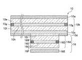
続いて、ミラー本体10および液晶モニタ16の内部構造について説明する。図2は、図1に示すミラー本体および液晶モニタの内部構造を示す断面図である。なお、図2では、ボディー1の内面側に位置する側を下側(背面側)、ボディー1の開口部1Aから外に覗く側を上側(前面側)に描いている。ミラー本体10は、図2中、上側から、偏光板10a、液晶セル10b、反射型偏光板(第二偏光板)10c、光吸収部材10dを重ねて貼付した構造になっている。また、液晶モニタ16が、ミラー本体10の反射型偏光板10cの背面側に配置される。なお、液晶モニタ16は、反射型偏光板10cに密着させてもよい。 Next, the internal structures of the
偏光板(第一偏光板)10aは、透過する偏光成分を選択するものであり、図2中上側から入射した入射光の特定の第一偏光成分を透過光として液晶セル10bに射出する。本実施形態では、第一偏光成分を、垂直偏光成分として説明する。また、偏光板10aは、液晶セル10bから入射する第一偏光成分の入射光をそのまま透過して透過光として、図2中上側に射出する。なお、運転者は、射出される透過光を網膜に結像することで、後方を確認できる。 The polarizing plate (first polarizing plate) 10a selects a polarized component to be transmitted, and emits a specific first polarized component of incident light incident from the upper side in FIG. 2 to the
液晶セル10bは、偏光板10aの背面に配置され、かつ、独立に制御可能な二つの制御領域を形成したものであり、制御領域ごとに光の透過のシャッターとして機能する。この液晶セル10bは、制御領域ごとに独立した図示しない透明電極が配線されている。透明電極はガラス基板10e,10fに形成され、ガラス基板10e,10f同士の間に形成された空間に液晶10hが封入されている。なお、液晶10hは、TN(Twisted Nematic)液晶とする。つまり、各制御領域は、ガラス基板10e,10fの図示しない透明電極間に電圧を印加しない(非印加)ときに、入射光に対して旋光性を発現し、その透明電極間に電圧を印加した(印加)ときに、発現していた旋光性が解消する液晶配列になっている。ガラス基板10e,10fの間には、シール材(スペーサ)10gが配置されている。 The
反射型偏光板(第二偏光板)10cは、液晶セル10bの背面に配置され、かつ、直交する偏光成分の光のいずれか一方を透過させるとともに他方を反射するものである。なお、ここでは、反射型偏光板10cが、透過させる偏光成分を垂直偏光成分(第二偏光成分)とし、反射させる偏光成分を水平偏光成分(第三偏光成分)とする。つまり、第一偏光成分(垂直偏光成分)と第三偏光成分(水平偏光成分)とが直交し、かつ、第一偏光成分(垂直偏光成分)と第二偏光成分(垂直偏光成分)とが平行になっている。 The reflective polarizing plate (second polarizing plate) 10c is disposed on the back surface of the
ここで、反射型偏光板10cの構造について説明する。図3は、図2に示す反射型偏光板の構造を示す斜視図である。この反射型偏光板10cは、樹脂層10c1,10c2,10c3,…,10cn−3,10cn−2,10cn−1,10cnの多層光学フィルム構造体によって形成されている。この反射型偏光板10cは、反射面に対し角度を持って反射した光が部分的に偏光することを利用し、多段階(各樹脂層10cn)の反射を用いて直線偏光を作り出す。Here, the structure of the reflective
また、この実施形態では、偏光板10aおよび反射型偏光板10cは、屈折率異方性を有する樹脂層によって形成されている。この屈折率異方性を有する樹脂層は、例えば、ポリビニルアルコール−ヨウ素系の材料を用いて形成される。例えば、ポリビニルアルコールを屈折率異方性が生じるように種々の方向に引き延ばして、そのポリビニルアルコールの分子のらせんが種々の方向に向くように並べた後、ヨウ素溶液に浸すことによって、そのらせん中にヨウ素を取り込ませて屈折率異方性と偏光性とを持たせて形成される。なお、さらに、セルロース系のプラスチックフィルムで挟んで耐久性と機械的強度を持たせることが望ましい。 In this embodiment, the
また、偏光板10aおよび反射型偏光板10cは、屈折率異方性によって、液晶セル10bから射出される透過光に含まれる常光線およびこの常光線と異なる進行方向の異常光線を分離して、常光線のみを反射光として運転者の瞳に導くように射出することが可能になる。つまり、液晶セル10bによって射出された透過光が、液晶分子の挙動の乱れ等に基づくゆらぎやムラによる異常光線を含んでいたとしても、異常光線を取り除いて常光線のみを反射光として射出する。 Further, the
図2に戻って、光吸収部材10dについて説明する。この光吸収部材10dは、第二偏光板10cの背面に配置され、黒色塗装を施した膜やフィルムとして形成される。なお、反射型偏光板10cが射出する透過光は、垂直偏光成分(第二偏光成分)なので、この垂直偏光成分を吸収する偏光子を光吸収部材として用いてもよい。 Returning to FIG. 2, the
また、光吸収部材10dを形成した層の一部には、光透過部材10iが形成されている。この光透過部材10iは、ガラス等の透明物質によって形成される。また、空気層であってもよい。また、この光透過部材10iは、偏光板10aと同じ光透過特性を備え、或いは、反射型偏光板10cと同じ偏光成分の光透過特性を備えるものであってもよい。そのため、光透過部材10iは、反射型偏光板10cを厚く形成したものでもよい。この実施形態では、光透過部材10iは、垂直偏光成分を透過する。なお、光透過部材10iを備えずに、直接、液晶モニタ16を反射型偏光板10cに密着させるようにしてもよい。 Further, a
光透過部材10iの背面には、画像を形成する液晶モニタ(画像形成装置)16(図1参照)が配置されている。この液晶モニタ16は、光透過部材10iと反射型偏光板10dとを透過可能な偏光成分の画像光を少なくとも射出するものである。また、液晶モニタ16Aの背面には、バックライト16Eが配置されている。液晶モニタ16では、表示する画像データに従って、アクティブマトリックスの画素に対応する各透明電極をオン・オフして、画素ごとの透過率を設定し、バックライト16Eからの光を液晶セル16Aに透過させることによって画像を形成する。 A liquid crystal monitor (image forming apparatus) 16 (see FIG. 1) for forming an image is disposed on the back surface of the
液晶セル16Aには、前記したように、アクティブマトリックス透明電極が配線されている。透明電極はガラス基板16B,16Cに形成され、ガラス基板16B,16C同士の間に形成された空間に液晶16Fが封入されている。ガラス基板16B,16Cの間には、シール材(スペーサ)16Dが配置されている。なお、前記したように、液晶セル16Aには、アクティブマトリックスに応じた画素を形成するブラックマトリックス(不図示)やカラーフィルター(不図示)が備えられている。 As described above, the active matrix transparent electrode is wired in the
次に、前記構成の液晶防眩ミラー100の非防眩時の動作および防眩時の画像の表示・非表示時動作について説明する。なお、以下、垂直偏光成分に記号「⊥」の下添字を付し、水平偏光成分に記号「=」の下添字を付して説明する。また、図4〜図7に示す領域AR1,領域AR2は、偏光板10aの表面の仮想的な領域を示すものとする。そして、領域AR2は、液晶モニタ16の前面、および、液晶セル10bの一方の制御領域の前面に位置している。また、領域AR1は、光吸収部材10dの前面に位置し、液晶セル10bの他方の制御領域に位置している。Next, the non-glare operation and the non-glare image display / non-display operation of the liquid crystal
まず、非防眩・非表示時について説明する。図4は、実施形態の液晶防眩ミラーの非防眩・非表示時の動作を説明する図であり、図4の(a)は非防眩・非表示時の液晶防眩ミラーの正面図、図4の(b)は非防眩・非表示時のミラー本体内の光の伝播の様子を示す模式図である。 First, the case of non-glare and non-display will be described. FIG. 4 is a diagram for explaining the operation of the liquid crystal anti-glare mirror according to the embodiment during non-glare / non-display, and FIG. 4A is a front view of the liquid crystal anti-glare mirror during non-glare / non-display. FIG. 4B is a schematic diagram showing a state of light propagation in the mirror body when non-glare is not displayed.
図4の(a)に示すように、液晶防眩ミラー100では、リング11によって囲われたミラー本体10の表面に、入射光の垂直偏光成分の略すべてが反射されている様子を示している。このとき、図4の(b)に示すように、領域AR1および領域AR2ともにスイッチSA,SBがオフされているため、電源Eからの交流電圧は、液晶セル10bに印加されていない。なお、スイッチSAは、液晶セル16Aに交流電圧が供給されている場合を「オン」、それが供給されていない場合を「オフ」とする。そのため、スイッチSAがオフとは、スイッチ8A(図1参照)がオフの場合に限らず、スイッチ8Aがオンの場合であっても、前記した周囲光センサの出力が後方光センサ7Bの出力よりも高いときも該当する。また、スイッチSBは、画像の表示・非表示なので、スイッチ8Bのオン・オフに対応する。そのため、画像が非表示なら、スイッチSBはオフである。As shown in FIG. 4A, the liquid
したがって、TN液晶としての液晶セル10bは、スイッチSA,SBともにオフで、液晶分子xが、図4中、垂直方向(電極方向に対して水平方向)に向き、かつ、水平方向(電極方向に対して垂直方向)にらせん状に配置されて、旋光性を有している。なお、電極方向は、図示しない透明電極を配線したガラス基板10e,10f(図2参照)の方向である(以下、明細書中において同じ)。 Accordingly, in the
図4の(b)に示すように、領域AR1および領域AR2ともに、光H1(自然光(特に後方光))が偏光板10aに入射すると、偏光板10aは垂直偏光成分(第一偏光成分)を透過し、光H2⊥を射出する。その光H2⊥は、液晶セル10bに入射し、その旋光性によって、略90度回転させられて、水平偏光成分(第三偏光成分)として光(常光線)H3=を射出する。このとき、液晶セル10b内の液晶分子の挙動が乱れている場合には、ゆらぎやムラによる光(異常光線)H4が光H3=に混ざって射出される。なお、光H4は、ゆらぎ等で光H3=の進行方向が異なったものなので、光H3=と同じ水平偏光成分であると考えられる、ここでは旋光されない垂直偏光成分も含めて考える。As shown in FIG. 4B, when light H1 (natural light (especially backward light)) is incident on the
液晶セル10bから射出された光H3=は、反射型偏光板10cに入射するが、水平偏光成分(第三偏光成分)なので、光H5=として反射される。すると、その光H5=は、液晶セル10bに入射して旋光されて、再び垂直偏光成分の光H6⊥として液晶セル10bから射出され、さらに、偏光板10aから光H8⊥として射出される。なお、液晶セル10b内の液晶分子の挙動が乱れている場合には、ゆらぎやムラによる光(異常光線)H7が光H6⊥に混ざって射出される。また、光H7は、ゆらぎ等で光H6⊥の進行方向が異なったものなので、光H6⊥と同じ垂直偏光成分であると考えられるが、ここでは旋光されない水平偏光成分も含めて考える。The light H3 = emitted from the
このとき、反射型偏光板10cでは、光H4の水平偏光成分の光H4=は、大きく曲げられて、光H5=の進行方向から外れ分離される。また、光H4の水平偏光成分の光H4⊥は、反射型偏光板10cを透過して、光吸収部材10dに吸収される。偏光板10aでは、光H7の水平偏光成分の光H7=は、大きく曲げられて、光H6⊥の進行方向から外れ分離される。また、光H7の水平偏光成分の光H7=は、偏光板10aに吸収され熱として放射される。At this time, the
したがって、この液晶防眩ミラー100は、非防眩・非表示時に、液晶セル10bでゆらぎ等によって異常光線が生じたとしても、偏光板10aや反射型偏光板10cによって異常光線を取り除いて常光線のみを反射光として射出するため、液晶セル10bで生じたゆらぎやムラの影響を受け難くなる。 Therefore, the liquid
続いて、防眩・非表示時について説明する。図5は、実施形態の液晶防眩ミラーの防眩・非表示時の動作を説明する図であり、図5の(a)は防眩・非表示時の液晶防眩ミラーの正面図、図5の(b)は防眩・非表示時のミラー本体内の光の伝播の様子を示す模式図である。なお、この防眩、つまり入射する光を吸収する場合、スイッチSA,SBともにオンになるため、防眩・非表示時には、液晶セル10bの領域AR1,AR2には電圧が印加される。そのため、ゆらぎが生じても直ぐに減衰すると考えられるが、ここではゆらぎが生じている場合について説明する。Next, the case of anti-glare / non-display will be described. FIG. 5 is a diagram for explaining the operation of the liquid crystal anti-glare mirror according to the embodiment during anti-glare / non-display. FIG. 5A is a front view of the liquid crystal anti-glare mirror during anti-glare / non-display. FIG. 5B is a schematic diagram showing a state of light propagation in the mirror body during anti-glare / non-display. Note that when anti-glare, that is, when absorbing incident light, both the switches SA and SB are turned on, a voltage is applied to the areas AR1 and AR2 of the
防眩・非表示時、領域AR1,AR2では、液晶分子xが、図5中、水平(平行)方向に向き、かつ、周囲光と後方光との光量の関係に基づいて、液晶セル10bに電圧が印加されて、電圧値に基づいて旋光性が一部解消される。つまり、液晶セル10bは、垂直偏光成分および水平偏光成分の両方を射出する。したがって、周囲光と後方光との比較によって偏光量が調節されるため、第二偏光板10cを反射して、再び、液晶セル10bを透過して偏光板10aが射出される光量を調節することができる。In anti-glare / non-display, in the areas AR1 and AR2 , the liquid crystal molecules x are oriented in the horizontal (parallel) direction in FIG. 5 and are based on the relationship between the amount of ambient light and back light. A voltage is applied to 10b, and the optical rotation is partially canceled based on the voltage value. That is, the
このように、この実施形態では、液晶セル10bに印加する電圧値を、周囲光と後方光との光量に応じた大きさに制御するものとするが、防眩時には、すべての液晶分子xが電極に対して略垂直に並ぶ程の大きさの電圧値を常に液晶セル10bに印加するようにしてもよい。液晶防眩ミラー100では、実際には、偏光板10aの表面が反射したり、偏光板10aの表面に重ねた保護膜(不図示)が反射したりするので、すべての入射光を光吸収部材10dで吸収させるように制御しても、運転者が後方光を目視することができるからである。なお、後方光の光量に応じて段階的に又は徐々に変化させて、眩しさを低減させるようにしてもよい。 As described above, in this embodiment, the voltage value applied to the
図5の(a)に示すように、液晶防眩ミラー100では、リング11によって囲われたミラー本体10の表面に、入射光の垂直偏光成分の略すべてが反射されている様子を示している。このとき、図5の(b)に示すように、スイッチSがオンされているため、電源Eからの交流電圧は、液晶セル10bに印加されていない。したがって、液晶セル10bは、TN液晶なので、液晶分子xが、図5中、垂直方向に向き、かつ、水平方向にらせん状に配置されて、旋光性を有している。 As shown in FIG. 5A, the liquid
図5の(b)に示すように、領域AR1および領域AR2ともに、光H1(自然光(特に後方光))が偏光板10aに入射すると、偏光板10aは垂直偏光成分(第一偏光成分)を透過し、光H2⊥を射出する。その光H2⊥は、液晶セル10bに入射し、その旋光性によって、その一部が、略90度回転させられて、水平偏光成分(第三偏光成分)として光(常光線)H9=を射出するとともに、残りの一部が、垂直偏光成分(第二偏光成分)として光(常光線)H10⊥を射出する。このとき、液晶セル10b内の液晶分子の挙動が乱れている場合には、ゆらぎやムラによる光(異常光線)H11が光H9=と光H10⊥とに混ざって射出される。なお、光H11は、ゆらぎ等で光H9=の進行方向が異なったものなので、光H9=と同じ水平偏光成分であると考えられるが、ここでは旋光されない垂直偏光成分も含めて考える。As shown in FIG. 5B, when light H1 (natural light (especially backward light)) is incident on the
液晶セル10bから射出された光H9=は、反射型偏光板10cに入射するが、水平偏光成分(第三偏光成分)なので、光H12=として反射される。すると、その光H12=は、液晶セル10bに入射して旋光されて、再び垂直偏光成分の光H13⊥として液晶セル10bから射出され偏光板10aに入射され、また、そのまま水平偏光成分の光H13=として射出され偏光板10aに入射される。偏光板10aでは、光H13⊥のみを透過して、光H15⊥として射出される。なお、液晶セル10b内の液晶分子の挙動が乱れている場合には、ゆらぎやムラによる光(異常光線)H14が光H13⊥と光H13=に混ざって射出される。光H14は、ゆらぎ等で光H13⊥の進行方向が異なったものなので、光H13⊥と同じ垂直偏光成分と考えられるが、ここでは旋光されない水平偏光成分も含めて考える。The light H9 = emitted from the
このとき、反射型偏光板10cでは、光H11の水平偏光成分の光H11=は、大きく曲げられて、光H12=の進行方向から外れ分離される。また、光H11の水平偏光成分の光H11⊥は光H9⊥とともに、反射型偏光板10cを透過する。光H11⊥と光H9⊥とは、領域AR1では光吸収部材10dに吸収され、領域AR2では液晶セル16Aに吸収および反射される。なお、光吸収部材10dと液晶セル16Aとでは、通常光吸収率が異なり、図5の(a)に示すように、領域AR2と領域AR1とのコントラストが異なり若干明るくなるため、できる限りコントラストが同じになるように液晶セル16Aの光吸収率を設定することが望ましい。At this time, the
一方、偏光板10aでは、光H14の水平偏光成分の光H14=は、大きく曲げられて、光H13⊥の進行方向から外れ分離される。また、光H14の水平偏光成分の光H14=は、光H13=とともに偏光板10aに吸収され熱として放射される。On the other hand, the
したがって、この液晶防眩ミラー100は、防眩時に、液晶セル10bでゆらぎ等によって異常光線が生じたとしても、偏光板10aや反射型偏光板10cによって異常光線を取り除いて常光線のみを反射光として射出するため、液晶セル10bで生じたゆらぎやムラの影響を受け難くなる。 Therefore, even if an extraordinary ray is generated due to fluctuation or the like in the
次に、非防眩・表示時について説明する。図6は、実施形態の液晶防眩ミラーの非防眩・表示時の動作を説明する図であり、図6の(a)は非防眩・表示時の液晶防眩ミラーの正面図、図6の(b)は非防眩・表示時のミラー本体内の光の伝搬の様子を示す模式図である。なお、スイッチSAは、非防眩時なので、オフである。つまり、領域AR1の様子は、図4に示した非防眩の場合と同じであるので、説明を省略する。一方、スイッチSBは、表示時なので、オンになる。つまり、領域AR2の光H1が入射したときの様子は、図5に示した防眩・非表示時の場合と同じである。そのため、以下では、液晶モニタ16が射出する画像光(I1⊥,I2⊥,I3⊥,I4⊥)の伝搬の様子について説明する。なお、スイッチSBのオンの信号は、図示しない配線を通して、液晶モニタ16にタイミング信号として出力され、液晶モニタ16がオンになる。Next, non-glare / display will be described. FIG. 6 is a diagram for explaining the operation of the liquid crystal anti-glare mirror according to the embodiment during non-glare / display, and FIG. 6A is a front view of the liquid crystal anti-glare mirror during non-glare / display, FIG. 6 (b) is a schematic diagram showing a state of light propagation in the mirror body during non-glare display and display. Note that the switch SA is off because it is not anti-glare. In other words, state of the region AR1 is the same as for a non-antiglare shown in FIG. 4, the description thereof is omitted. On the other hand, the switch SB is turned on because it is displaying. In other words, state where light H1 region AR2 is incident is the same as that of the antiglare-hidden when shown in Fig. Therefore, in the following, the state of propagation of image light (I 1,, I 2,, I 3⊥ , I 4⊥ ) emitted from the liquid crystal monitor 16 will be described. Note that the ON signal of the switch SB is output as a timing signal to the liquid crystal monitor 16 through a wiring (not shown), and the liquid crystal monitor 16 is turned on.
液晶モニタ16では、液晶セル16Aに画像データが伝送されると、画像データに基づいて画素ごとの透明電極がオン・オフされ、バックライト16Eの点灯によって、画像光I1⊥が射出される。画像光I1⊥は、反射型偏光板10cに入射して、その偏光状態のまま画像光I2⊥として射出される。その画像光I2⊥は、液晶セル10bに入射すると、その偏光状態のまま画像光I3⊥として射出される。その画像光I3⊥は、偏光板10aを透過できるため、その偏光状態のまま偏光板10aから画像光I4⊥として射出される。したがって、液晶セル16Aから射出された画像光I1⊥は、透過損失の少ない光学系を伝搬していくため、略同じ光量の画像光I4⊥として射出される。そのため、図6の(a)に示すように、領域AR1が非防眩時に、領域AR2内には、明るい画像が表示される。In the
次に、防眩・表示時について説明する。図7は、実施形態の液晶防眩ミラーの防眩・表示時の動作を説明する図であり、図7の(a)は防眩・表示時の液晶防眩ミラーの正面図、図7の(b)は防眩・表示時のミラー本体内の光の伝搬の様子を示す模式図である。なお、スイッチSAは、防眩時なので、オンである。つまり、領域AR1の様子は、図5に示した防眩の場合と同じであるので、説明を省略する。一方、スイッチSBは、表示時なので、オンになる。つまり、領域AR2の光H1が入射したときの様子は、図5に示した防眩・非表示時の場合と同じである。また、領域AR2での画像光(I1⊥,I2⊥,I3⊥,I4⊥)の伝搬の様子は、図6に示した表示の場合と同じであるので、詳細な説明を省略するが、液晶セル16Aから射出された画像光I1⊥は、透過損失の少ない光学系を伝搬していくため、略同じ光量の画像光I4⊥として射出される。そのため、図7の(a)に示すように、領域AR1が防眩時に、領域AR2内には、明るい画像が表示される。したがって、防眩・表示と非防眩・表示とを比較すると、領域AR1が防眩か非防眩かに係わらず、領域AR2からは画像光I4⊥が射出される。Next, the anti-glare / display time will be described. FIG. 7 is a diagram for explaining the operation of the liquid crystal antiglare mirror according to the embodiment at the time of antiglare / display. FIG. 7A is a front view of the liquid crystal antiglare mirror at the time of antiglare / display, and FIG. (B) is a schematic diagram which shows the mode of propagation of the light in the mirror main body at the time of glare-proof and display. The switch SA is on because it is anti-glare. In other words, state of the region AR1 is the same as that of the antiglare shown in FIG. 5, the description thereof is omitted. On the other hand, the switch SB is turned on because it is displaying. In other words, state where light H1 region AR2 is incident is the same as that of the antiglare-hidden when shown in Fig.Further , the state of propagation of the image light (I 1⊥ , I 2,, I 3⊥ , I 4⊥ ) in the area AR2 is the same as the display shown in FIG. omitted, the image light I1⊥ emitted from the
最後に、液晶セル10bを制御する液晶セル制御回路(手段)の例1,2について説明する。図8は、液晶セル制御回路の例1を説明する回路図である。図9は、液晶セル制御回路の例2を説明する回路図である。なお、液晶セル制御回路は、図1に示したプレートサーキット7に形成される。 Finally, examples 1 and 2 of the liquid crystal cell control circuit (means) for controlling the
[例1]
図8に示すように、一端をアースされた直流の電源Eの正極が分岐点J1でスイッチS1とスイッチS2とに接続されている。スイッチS1には、分岐点J2を介して、分岐点J53と抵抗R1とが接続されている。一方、スイッチS2には、分岐点J52を介して、回路OR1の入力端子と、LSIのA入力端子とが接続されている。LSIは、液晶セル16Aおよびバックライト16Eの制御を行うものである。このLSIのB出力端子およびC出力端子には液晶セル16Aの端子が接続されている。また、LSIのD出力端子には、バックライト16Eが接続されている。このLSIは、スイッチS2がオンのときに、A入力端子の入力を契機として、B出力端子とC出力端子とに交流電圧を印加し、E入力端子から入力される画像データに基づいて液晶セル16Aの画素ごとの透過率を設定し、バックライト16Eを点灯させて、液晶セル16Aから画像光を射出させる。[Example 1]
As shown in FIG. 8, the positive electrode of the DC power source E, which is grounded at one end is connected to a switch S1 and switch S2 at a branch point J1. The switchS 1, via a branch pointJ 2, a branch pointJ 53 and resistorR 1 is connected. On the other hand, the switchS 2, via a branch pointJ 52, an input terminal of the circuit OR1, and the A input terminal of the LSI are connected. The LSI controls the
ところで、抵抗R1には、周囲光センサ7Cと後方光センサ7Aとが直列に接続されている。なお、後方光センサ7Aの他端はアースされている。また、周囲光センサ7Cと後方光センサ7Aとの間の分岐点J3には、シュミットホールドインバータ回路(以下「回路SHI」と称する)SHI1が接続されている。なお、周囲光センサ7Cと後方光センサ7Aとは、受光量が増加すれば、出力電圧値が上昇するフォトダイオードとする。Incidentally, the resistor R1, and the ambient light sensor 7C and the backward
分岐点J3と回路SHI1の入力端子との間の配線には、分岐点J4から一端をアースされた抵抗R2が接続され、分岐点J5から一端をアースされたコンデンサC1が接続されている。この抵抗R2およびコンデンサC1は、分岐点J3の電圧変化による信号が、回路SHI1の入力端子に入力するのを遅延させる遅延回路(手段)として機能する。回路SHI1の出力端子側には、回路SHI2の入力端子が接続されている。A resistor R2 having one end grounded from the branch point J4 is connected to the wiring between the branch point J3 and the input terminal of the circuit SHI1 , and a capacitor C1 having one end grounded from the branch point J5 is connected to the wiring. It is connected. The resistor R2 and the capacitor C1 function as a delay circuit (means) that delays the signal due to the voltage change at the branch point J3 from being input to the input terminal of the circuit SHI1 . The input terminal of the circuit SHI2 is connected to the output terminal side of the circuit SHI1 .
なお、回路SHI1等は、ヒステリシス特性を有しているため、設定されている範囲の多少の電圧変動によっては動作状態を変更しない。回路SHI1の負論理が、回路SHI2で正論理に戻され、上下の電圧の変動分が、回路SHI1,SHI2のヒステリシス特性によって吸収されるようになっている。Since the circuit SHI1 and the like have hysteresis characteristics, the operation state is not changed by a slight voltage fluctuation within the set range. The negative logic of the circuit SHI1 is returned to the positive logic by the circuit SHI2 , and fluctuations in the upper and lower voltages are absorbed by the hysteresis characteristics of the circuits SHI1 and SHI2 .
また、回路SHI2の出力端子は、分岐点J51で二つに分岐し、一方は領域AR1の制御回路α1内の分岐点J6に接続され、他方は回路OR1の入力端子に接続されている。そして、回路OR1の出力端子が、領域AR2の制御回路α2内の分岐点J6に接続されている。なお、二つの制御回路α1,α2は、同じ電子部品および配線からなる。ただし、後記する論理回路NAND2と論理回路NAND4との接続先が異なる。つまり、制御回路α1の論理回路NAND2と論理回路NAND4とが領域AR1の透明電極に接続され、制御回路α2の論理回路NAND2と論理回路NAND4とが領域AR1の透明電極に接続される。そこで、本実施形態に特徴的な、液晶モニタ16(図1等参照)を制御する制御回路α2の構成・機能について説明し、制御回路α1については説明を省略する。なお、各制御回路α1,α2の分岐点J30は、分岐点J53を介して分岐点J2に接続されている。また、制御回路α1,α2内の同じ電子部品や分岐点には、同一符号を付して説明する。Further, the output terminal of the circuit SHI2 branches into two at the branch point J51 , one is connected to the branch point J6 in the control circuit α1 in the area AR1 , and the other is connected to the input terminal of the circuit OR1. It is connected. The output terminal of the circuit OR1 is connected to the branch point J6 in the control circuit α2 in the area AR2 . The two control circuits α1 and α2 are composed of the same electronic components and wiring. However, the connection destination of the logic circuit NAND2 and the logic circuit NAND4 which will be described later is different. That is, the logic circuit NAND2 and the logical circuit NAND4 of the control circuit alpha1 is connected to the transparent electrodes in the area AR1, the control circuit alpha2 logic circuit NAND2 and the transparent electrode of the logic circuit NAND4 and the area AR1 Connected to. Therefore, the present embodiment characteristic of the
分岐点J6には、ディジタルIC1のB入力端子に入力されている。このディジタルIC1は、ディジタルIC2とともに発振回路(手段)として機能する。ディジタルIC1,IC2は、A入力端子(負論理)(図1中、符号Aの上部には、記号「−」を付して表しているが、明細書中では、表記上省略する。)、B入力端子、Q出力端子(正論理)、Q出力端子(負論理)(同様に、記号「−」を、表記上省略する。)、CLR端子、Cx端子、Rx/Cx端子が備えられている。The branch point J6 is inputted to the B input terminal of the digital IC1 . This digital IC1 functions as an oscillation circuit (means) together with the digital IC2 . The digital IC1 and IC2 are represented by an A input terminal (negative logic) (in FIG. 1, the symbol “-” is attached to the upper part of the symbol A, but is omitted in the specification for the sake of description. ), B input terminal, Q output terminal (positive logic), Q output terminal (negative logic) (similarly, the symbol “-” is omitted in the notation), CLR terminal, Cx terminal, Rx / Cx Terminals are provided.
また、分岐点J6には、抵抗R3が接続され、抵抗R3の他端側の分岐点J7には、一端をアースされたコンデンサC2が接続されている。また、その分岐点J7には、分岐点J8へと続く配線が接続され、その分岐点J8が、ディジタルIC1,IC2のCLR端子のそれぞれに接続されている。そのため、抵抗R3およびコンデンサC2は、CLR端子へ入力する信号を遅延させる。Also, the branch point J6, the resistor R3 is connected to the other end side of the branch point J7 of the resistor R3, a capacitor C2, which is grounded at one end is connected. Further, the branch point J7 is connected to the wiring that continues to the branch point J8 , and the branch point J8 is connected to each of the CLR terminals of the digital IC1 and IC2 . Therefore, the resistanceR 3 and capacitorC 2 delays the signal input to the CLR terminal.
また、回路SHI2の出力端子と、ディジタルIC1のB入力端子との間の配線の分岐点J9には、ディジタルIC2のB入力端子が分岐点J10を介して接続されている。そのため、ディジタルIC1,IC2の各B入力端子には、回路SHI2からの同じ出力が入力される。Further, an output terminal of the circuit SHI2, the branch pointJ 9 of the wiring between the B input terminal of the digital IC1, B input terminal of the digital IC2 is connected via a branch pointJ 10. Therefore, the same output from the circuit SHI2 is input to each B input terminal of the digital IC1 and IC2 .
ディジタルIC1のQ出力端子(正論理)は、ディジタルIC2のA入力端子(負論理)とに接続されている。また、ディジタルIC1のQ出力端子(負論理)は開放している。ディジタルIC2のQ出力端子(正論理)は、分岐点J11を介して、ディジタルIC1のA入力端子(負論理)に入力している。したがって、ディジタルIC1,IC2のB入力端子がH(high)のとき、ディジタルIC2のQ出力端子(正論理)がL(Low)であれば、ディジタルIC2のQ出力端子(負論理)がLになり、結局、ディジタルIC1はQ出力端子(正論理)をHとし、開放されたQ出力端子(負論理)をLとする。そして、Rx/Cx端子で設定された時定数に基づいたデューティー比に従って、ディジタルIC1のQ出力端子(正論理)がLになると、ディジタルIC2のA入力端子(負論理)がLになる。すると、ディジタルIC2のQ出力端子(正論理)がHになるとともに、Q出力端子(負論理)がLになる。以上を繰り返すことによって、B端子がHのとき、ディジタルIC1,IC2は、発振回路(手段)として機能する。Digital IC1 of output terminal Q (positive logic) is connected to the digital IC2 A input terminal (negative logic). The Q output terminal (negative logic) of the digital IC1 is open. Digital IC2 Q output terminal (positive logic), via a branch pointJ 11, are input to the input terminal A digital IC1 (negative logic). Accordingly, when the B input terminal of the digitalIC 1, IC2 is H of (high), if the digital IC2 Q output terminal (positive logic) is a L (Low), the digital IC2 Q output terminal (negative logic ) is L, and eventually, the digital IC1 'Q output terminal (positive logic) and H, is opened Q output terminal (negative logic) and L. When the Q output terminal (positive logic) of the digital IC1 becomes L in accordance with the duty ratio based on the time constant set at the Rx / Cx terminal, the A input terminal (negative logic) of the digital IC2 becomes L become. Then, the Q output terminal (positive logic) of the digital IC2 becomes H, and the Q output terminal (negative logic) becomes L. By repeating the above, when the B terminal is H, the digital IC1 and IC2 function as an oscillation circuit (means).
ところで、ディジタルIC1のCx端子は、一端をアースとコンデンサCxとの間の分岐点J12に接続されている。コンデンサCxは、他端側に分岐点J13を介して、Rx/Cx端子に接続されている。分岐点J13には、分岐点J14,J15を介して、ディジタルIC2のRx/Cx端子に接続されている。なお、ディジタルIC2のCx端子は、アースされている。また、分岐点J14には、分岐点J14側を負極端子としたダイオードD1が接続されている。分岐点J15には、抵抗Rxが接続されている。Meanwhile,C x terminal of the digital IC1 'is connected to a branch pointJ 12 between the ground and the capacitorC x one end. The capacitor Cx is connected to the Rx / Cx terminal via the branch point J13 on the other end side. The branch pointJ 13, via a branch pointJ 14,J15, are connected to theR x /C x terminal of the digital IC2. TheCx terminal of the digital IC2 is grounded. Also, the branch point J14, diode D1 is connected with a branch point J14 side and the negative terminal. The branch pointJ 15, resistorR x is connected.
また、ダイオードD1の正極側端子および抵抗Rxの他端側は、分岐点J31に接続され、分岐点J2を介して電源Eの正極側に接続されている。そのため、コンデンサCxは、スイッチSがオンされたときに、抵抗Rxを介して充電されている。スイッチSがオフされたときに、放電が開始され、ディジタルIC1の端子Cxの電位を上昇させる。これによって、ディジタルIC1が、急激に、オフしないように、遅延回路(手段)として機能する。なお、スイッチSがオンのときには、ディジタルIC1,IC2は、それぞれRx/Cx端子から駆動電力を供給される。The positive electrode side other end side of the terminal and the resistor Rx of the diode D1 is connected to a branch point J31, it is connected to a positive electrode side of the power supply E via the branch point J2. Therefore, the capacitorCx is charged via the resistorRx when the switch S is turned on. When the switch S is turned off, the discharge is started, raising the potential of the terminal Cx of the digital IC1. Thus, the digital IC1 functions as a delay circuit (means) so as not to be turned off suddenly. When the switch S is on, the digital IC1 and IC2 are respectively supplied with driving power from the Rx / Cx terminals.
また、分岐点J11は、論理回路NAND1のA入力端子に接続されている。論理回路NAND1のC出力端子は、論理回路NAND2のA,B入力端子に接続されている。論理回路NAND2のC出力端子は、液晶セル10bの領域AR2の一端側の端子に接続される。また、分岐点J16が、論理回路NAND1のB入力端子と、論理回路NAND3のB入力端子に接続されている。The branch point J11 is connected to the A input terminal of the logic circuit NAND1. The C output terminal of the logic circuit NAND1 is connected to the A and B input terminals of the logic circuit NAND2 . The C output terminal of the logic circuit NAND2 is connected to a terminal on one end side of the area AR2 of the
論理回路NAND3のA入力端子は、ディジタルIC2のQ出力端子(負論理)に接続されている。また、論理回路NAND3のC出力端子は、論理回路NAND4のA,B入力端子に接続されている。論理回路NAND4のC出力端子は、液晶セル10bの領域AR2の他端側の端子に接続される。The A input terminal of the logic circuit NAND3 is connected to the Q output terminal (negative logic) of the digital IC2 . Also, C output terminal of the logic circuit NAND3 are connected A logic circuit NAND4, the B input terminal. An output terminal C of the logical circuit NAND4 is connected to the other end of the terminal area AR2 of the
そのため、液晶セル10bの領域AR2(領域AR1)が非印加となるためには、論理回路NAND2,論理回路NAND4のC出力端子が、両方共にLである。一方、液晶セル10bが印加となるためには、論理回路NAND2,論理回路NAND4のいずれか一方のC出力端子がHで、他方のC出力端子がLとなる。Therefore, in order for the area AR2 (area AR1 ) of the
以上の例1の回路では、周囲光センサ7Cと後方光センサ7Aとの間の分岐点J3の電圧値に基づいて、液晶セル10bのオン・オフが行われる。以下、非防眩時と防眩時とに分けて、作動状態について説明する。ところで、回路OR1は、後方光センサ7Aの出力電圧が大きくなったとき、つまり、分岐点J3の電圧が高くなっとき、または、スイッチS2がオンで液晶モニタ16を表示制御のときに、Hが出力され、前記したようにして、領域AR2に交流電圧を印加し、画像を表示させる。In the circuit example 1 above, based on the voltage value of the branch point J3 between the surrounding light sensor 7C and the backward
まず、周囲が明るいときに、後方光が照射された場合を説明する。この場合、後方光が周囲光に紛れてしまって、運転者は眩しく感じないので、領域AR2が表示か否かにかかわらず、領域AR1は非防眩状態に制御する。つまり、この場合、周囲光センサ7Cの受光量が大きくて、その出力電圧が高く、後方光センサ7Aの受光量が大きくなっても、分岐点J3の電圧値が高くならないので、回路SHI1の入力端子はL(Low)になる。このとき、回路SHI1の出力がH(High)であり、結局、回路SHI2の出力はLになる。そのため、制御回路α1では、ディジタルIC1,IC2の各B入力端子および各CLR端子はLである。また、論理回路NAND1,論理回路NAND3の各B入力端子がLなので、論理回路NAND1,論理回路NAND3の各C出力端子はHになり、論理回路NAND2,論理回路NAND4の各C出力端子はLになっている。つまり、領域AR1は非印加であって、液晶防眩ミラー100の領域AR1としては非防眩状態になっている。First, the case where the back light is irradiated when the surroundings are bright will be described. In this case, the back light is mixed with the ambient light and the driver does not feel dazzling. Therefore, the area AR1 is controlled to be in the non-glare state regardless of whether the area AR2 is displayed. That is, in this case, large amount of light received ambient light sensor 7C, high output voltage, even if the received light volume of the backward
なお、前記非防眩の場合に非表示のときには、分岐点J51がLで、かつ、スイッチS2がオフで、回路OR1の出力がLで、制御回路AR2が作動しないため、前記したように、領域AR2は旋光性を呈し、領域AR1と同じ非防眩になっている。一方、表示のときには、分岐点J51がLで、かつ、スイッチS2がオンであって、制御回路AR1は作動しないが、制御回路AR2が作動するため、領域AR1は非印加で、かつ、領域AR2は交流電圧の印加で、非防眩かつ表示状態となる。In the case of non-display in the case of non-glare, the branch point J51 is L, the switch S2 is OFF, the output of the circuit OR1 is L, and the control circuit AR2 does not operate. as was the region AR2 exhibits optical activity, it has the same non-antiglare an area AR1. On the other hand, when the display is a branch pointJ 51 L, and the switchS 2 is an on, the control circuit AR1 does not operate, because the control circuit AR2 is operated, the area AR1 in the non-application and area AR2 in the application of the AC voltage, the non-glare and display state.
また、周囲が暗いときに、後方光が照射された場合には、後方光が強調されて、運転者は眩しく感じるので、防眩状態に制御する。つまり、この場合、周囲光センサ7Cの受光量が小さくて出力電圧が小さく、かつ、後方光センサ7Aの受光量が大きくて出力電圧が大きくなるので、分岐点J3の電圧値が高くなる。そのため、回路SHI1の入力端子がHになり、結局、回路SHI2の出力電圧がHになる。すると、制御回路α1では、論理回路NAND1,論理回路NAND2の各B入力端子がHになる。また、ディジタルIC1,IC2の各B入力端子がHになるので、発振回路として作動を開始する。そのため、論理回路NAND1,論理回路NAND2がディジタルIC2の出力に基づいてオン・オフを繰り返し、論理回路NAND2,論理回路NAND4のオン・オフを介して、液晶セル10bに交流電圧が印加されるので印加状態になり、液晶防眩ミラー100の領域AR1としては防眩状態になる。Further, when the back light is irradiated when the surroundings are dark, the back light is emphasized and the driver feels dazzling, so the anti-glare state is controlled. That is, in this case, lower output voltage a small amount of light received by the ambient light sensor 7C, and the output voltage increase amount of light received backward
また、防眩の場合には、非表示および表示のいずれのときにも、領域AR2に交流電圧を印加する。つまり、領域AR2が防眩の場合には、スイッチS2がオンであろうが、オフであろうが回路OR1には、Hが入力しているため、制御回路α2が作動状態になる。表示の場合には、スイッチS2がオンになって、LSIが作動し、液晶セル16Aから画像光が出力されるが、制御回路α2の作動状態は変わらない。In the case of antiglare, even if any hidden and display, an AC voltage is applied to the area AR2. That is, when the area AR2 is anti-glare, whether the switch S2 is on or off, H is input to the circuit OR1 , so that the control circuit α2 is in the operating state. Become. In the case of the display, the switch S2 is turned on, LSI is activated, the image light from the
[例2]
図9に示すように、例2の場合も例1の場合と同様に、一端をアースされた直流の電源Eの正極が分岐点J1でスイッチS1とスイッチS2とに接続されている。スイッチS1には、分岐点J2を介して、分岐点J53と、電源Eの正極が抵抗R1とに接続されている。一方、スイッチS2には、分岐点J52を介して、回路OR1の入力端子と、LSIのA入力端子とが接続されている。LSIは、液晶セル16Aおよびバックライト16Eの制御を行うものである。このLSIのB出力端子およびC出力端子には液晶セル16Aの端子が接続されている。また、LSIのD出力端子には、バックライト16Eが接続されている。このLSIは、スイッチS2がオンのときに、A入力端子の入力を契機として、B出力端子とC出力端子とに交流電圧を印加し、E入力端子から入力される画像データに基づいて液晶セル16Aの画素ごとの透過率を設定し、バックライト16Eを点灯させて、液晶セル16Aから画像光を射出させる。なお、例1と同じ部品には、同一符号を付してある。[Example 2]
As shown in FIG. 9, as in the case of Example 1 in the example 2, the positive electrode of the DC power source E, which is grounded at one end is connected to a switch S1 and switch S2 at a branch point J1 . The switchS 1, via a branch pointJ 2, a branch pointJ 53, the positive electrode of the power supply E is connected to the resistorR 1. On the other hand, the switchS 2, via a branch pointJ 52, an input terminal of the circuit OR1, and the A input terminal of the LSI are connected. The LSI controls the
ところで、抵抗R1には、周囲光センサ7Cと後方光センサ7Aとが直列に接続されている。なお、後方光センサ7Aの他端はアースされている。また、周囲光センサ7Cと後方光センサ7Aとの間の分岐点J3には、シュミットホールドインバータ回路(以下「回路SHI」と称する)SHI1が接続されている。なお、回路SHI1は、ヒステリシス特性を有しているため、設定されている範囲の多少の電圧変動によっては動作状態を変更しない。Incidentally, the resistor R1, and the ambient light sensor 7C and the backward
回路SHI1の負論理が、分岐点J51に接続されている。この分岐点J51には、領域AR1を制御する制御回路β1内の分岐点J17が接続されている。また、この分岐点J51には、回路OR2の負論理の入力端子が接続されている。また、この回路OR2の正論理の入力端子には、スイッチS2に至る分岐点J52が接続されている。そして、この回路OR2の出力端子は、負論理に設定されている。つまり、この回路OR2は、負論理の入力端子がLのとき、または、正論理の入力端子がHのときに、出力端子がLになるように設定されている。なお、回路OR2の出力端子は、領域AR2を制御する制御回路β2内の分岐点J17に接続されている。Negative logic circuit SHI1 is connected to a branch pointJ 51. The branch pointJ 51, branch pointJ 17 of the control circuit β1 for controlling the area AR1 is connected. Further, the negative logic input terminal of the circuit OR2 is connected to the branch point J51 . In addition, the positive logic input terminal of the circuit OR2, branch point J52 leading to the switch S2 is connected. The output terminal of the circuit OR2 is set to negative logic. That is, the circuit OR2 is set so that the output terminal becomes L when the negative logic input terminal is L or when the positive logic input terminal is H. Note that the output terminal of the circuit OR2 is connected to the branch point J17 in the control circuit β2 that controls the area AR2 .
この例2でも、本実施形態に特徴的な、液晶モニタ16(図1等参照)を制御する制御回路β2の構成・機能について説明し、制御回路β1については説明を省略する。分岐点J17には、ダイオードD4のアノードとダイオードD2のアノードとが接続されている。ダイオードD4のカソードには、分岐点J18を介して、一端をアースした抵抗R3が接続されている。この分岐点J18は、分岐点J19を介して、回路SHI8の入力端子に接続されている。回路SHI8の出力端子は、液晶セル10bの一方の端子に接続されている。In this example 2, the present embodiment characteristic of the
一方、ダイオードD2のカソードには、分岐点J20を介して、一端をアースした抵抗R4が接続されている。分岐点J20には、また、分岐点J21を介して、回路SHI7の入力端子が接続されている。回路SHI7の出力端子は、液晶セル10bの他方の端子に接続されている。したがって、液晶セル10bが非印加のときは、回路SHI7,回路SHI8の両方の出力端子がLであり、印加のときは、回路SHI7,回路SHI8の各出力端子が交互にHとLとを繰り返すことになる。On the other hand, the cathode of the diode D2, via a branch point J20, resistors R4 that grounding the one end is connected. The branch pointJ 20, also via a branch pointJ 21, is connected to the input terminal of the circuit SHI7. The output terminal of the circuit SHI7 is connected to the other terminal of the
また、分岐点J21と回路SHI7との間の分岐点J22には、回路SHI4の入力端子が接続され、その出力端子がダイオードD5を介して分岐点J19に接続されている。また、分岐点J21には、ダイオードD3のカソードが接続され、そのアノードには回路SHI6の出力端子が接続されている。そして、回路SHI6の入力端子には、分岐点J23を介して、回路SHI5の出力端子と、抵抗R5とが接続されている。また、回路SHI5の入力端子と抵抗R5とが分岐点J24で接続され、この分岐点J24を介して、一端をアースされたコンデンサC2に接続されている。Further, an input terminal of the circuit SHI4 is connected to the branch point J22 between the branch point J21 and the circuit SHI7, and an output terminal thereof is connected to the branch point J19 via the diode D5 . . Also, the branch point J21, is connected to the cathode of the diode D3, which is connected to the output terminal of the circuit SHI6 in the anode. The output terminal of the circuit SHI5 and the resistor R5 are connected to the input terminal of the circuit SHI6 via the branch point J23 . Further, an input terminal of the circuit SHI5 and resistor R5 is connected at a branch point J24, via the branch point J24, is connected to the capacitor C2, which is grounded at one end.
そのため、以上の回路では、非防眩時、つまり、分岐点J3がLのときには、回路SHI1の出力端子がHになるので、ダイオードD2が導通して、分岐点J21側がHになる。そのため、ダイオードD3には逆電圧が印加され、回路SHI6の出力端子がLとなり、その入力端子側の分岐点J23の電位がHになる。ところで、コンデンサC2と回路SHI5と抵抗R5とは無安定マルチバイブレータ(発振回路(手段))を構成しているので、分岐点J23がHになると、抵抗R5を通して、コンデンサC2が充電される。しかし、ダイオードD3に逆電圧が印加されているときには、回路SHI5のトリガ電圧を超えることはないので、分岐点J23はHのままで、コンデンサC2は飽和された状態を維持する。Therefore, in the circuit described above, when Hibomabayu, that is, when the branch point J3 of L, the output terminal of the circuit SHI1 is H, the diode D2 is conducting, the branch point J21 side is H Become. Therefore, the diode D3 reverse voltage is applied, the output terminal becomes L of the circuit SHI6, the potential of the branch point J23 of the input terminal side becomes H. Incidentally, the capacitor C2 , the circuit SHI5, and the resistor R5 constitute an astable multivibrator (oscillation circuit (means)). Therefore, when the branch point J23 becomes H, the capacitor C2 passes through the resistor R5. Is charged. However, when a reverse voltage to the diode D3 is applied, so does not exceed the trigger voltage of the circuit SHI5, the branch point J23 remains H, the capacitor C2 maintains a state of being saturated.
このとき、ダイオードD4は順方向に導通しているので、回路SHI8の入力端子がHとなり、その出力端子がLとなっている。また、ダイオードD2が導通しているので、回路SHI7の入力端子がHとなり、その出力端子がLとなっている。そのため、液晶セル10bは非印加であって、液晶防眩ミラー100としては非防眩状態になっている。なお、回路SHI4の入力端子もHであって、その出力端子はLであり、かつ、分岐点J19がHなので、ダイオードD5には順方向の電圧が印加されている。At this time, the diode D4 is because the conduct in the forward direction, the input terminal becomes H circuit SHI8, has its output terminal and L. Further, the diode D2 is conducting, the input terminal becomes H circuit SHI7, has its output terminal and L. Therefore, the
なお、前記非防眩の場合に非表示のときには、分岐点J51がHで、かつ、スイッチS2がオフで、回路OR2の出力がHであって、制御回路AR2が作動しないため、前記したように、領域AR2は旋光性を呈し、領域AR1と同じ非防眩になっている。一方、表示のときには、分岐点J51がLで、かつ、スイッチS2がオンであって、制御回路AR2が作動するため、領域AR2には交流電圧が印加され、表示状態となる。Note that the when hidden in the case of non-anti-glare is is H branch point J51, and the switch S2 is off, the output of the circuit OR2 is an H, the control circuit AR2 is not operated As described above, the area AR2 exhibits optical rotation and has the same non-glare resistance as the area AR1 . On the other hand, when the display is a branch point J51 L, and the switch S2 is a one, because the control circuit AR2 is operated, the area AR2 is applied an AC voltage, a display state.
この状態で、防眩時、つまり、分岐点J3がHになると、回路SHI1の出力端子(分岐点J51)がLになるので、制御回路β1では、ダイオードD2には逆電圧が掛かり、分岐点J21側は抵抗R4を通してLになっていく。一方、ダイオードD3の逆電圧によって回路SHI6の出力端子に掛かっていたLの電圧が低下するので、回路SHI6のトリガ電圧と回路SHI5のトリガ電圧のバランスによって、コンデンサC2の放電が始まり、コンデンサC2と回路SHI5と抵抗R5とによって発振が開始される。この発振はダイオードD3を通して分岐点J22側に伝わるので、回路SHI7の出力端子がHとLとの反転を繰り返し、かつ、回路SHI4と回路SHI8とによって回路SHI7の反転同期してその反転とは逆のLとHとの反転を繰り返すことになる。そのため、液晶セル10bの領域AR1が印加状態になり、液晶防眩ミラー100の領域AR1としては防眩状態になる。In this state, when an anti-glare, that is, when the branch pointJ 3 becomes H, the output terminal of the circuit SHI1 (branch pointJ 51) is L, and the control circuit beta1, the diodeD 2 inverse voltage consuming, it is the branch pointJ 21 side gradually becomes L through the resistorR 4. On the other hand, since the voltage of L applied to the output terminal of the circuit SHI6 is reduced by the reverse voltage of the diode D3 , the discharge of the capacitor C2 is caused by the balance between the trigger voltage of the circuit SHI6 and the trigger voltage of the circuit SHI5. beginning, oscillation is started by the capacitorC 2 and the circuit SHI5 and the resistorR 5. Since this oscillation is transmitted to the branch point J22 side through the diode D3, the output terminal of the circuit SHI7 repeats inversion of H and L, and the circuit SHI4 and the circuit SHI8 synchronize with the inversion of the circuit SHI7. Thus, the inversion of L and H opposite to the inversion is repeated. Therefore, the region AR1 of the
なお、前記防眩の場合に非表示のときには、分岐点J51がLで、かつ、スイッチS2がオフで、回路OR2の出力はLとなる。つまり、領域AR2は、領域AR1と同様に、印加状態となって、領域AR2としても防眩状態となる。一方、防眩の場合に表示のときには、非表示のときの同様に、分岐点J51がLであるので、領域AR1,AR2は印加状態になっている。また、スイッチS2がオンになるので、LSIが作動する。したがって、液晶防眩ミラー100では、液晶セル16Aとバックライト16Eとによって形成された画像光が、領域AR2から射出される。Note that when the non-display in the case of the anti-glare is a branch point J51 L, and the switch S2 is off, the output of circuit OR2 becomes L. In other words, the area AR2, like the area AR1, becomes applied state, it is anti-glare state as an area AR2. On the other hand, when displaying in the case of anti-glare, since the branch pointJ51 is L as in the case of non-display, the areas AR1 and AR2 are in an applied state. Further, the switchS 2 is turned on, LSI is operated. Therefore, in the liquid crystal glare-
したがって、この実施形態の液晶防眩ミラー100によれば、透過損失の少ない光学系によって画像光を伝搬させて明るい画面を表示することが可能になる。また、この液晶防眩ミラー100は、偏光板10a、液晶セル10bおよび反射型偏光板10c等のような光学系で構成しているため、たとえ入射面で画像光の一部を反射していたとしても、反射と透過とを略同等に扱うハーフミラーのように、透過光の光量が落ちる訳ではない。 Therefore, according to the liquid
[変形例1]
この実施形態では、周囲光センサ7Cおよび後方光センサ7Aの両方を設けた場合を説明したが、その一方を備えているようにしてもよい。[Modification 1]
In this embodiment, the case where both the ambient light sensor 7C and the
[変形例2]
この実施形態では、光の透過シャッターとして、TN液晶の場合を説明したが、シャッター機能を備えるものであれば、TN液晶に限らない。[Modification 2]
In this embodiment, the case of the TN liquid crystal is described as the light transmission shutter. However, the light transmission shutter is not limited to the TN liquid crystal as long as it has a shutter function.
[変形例3]
この実施形態では、光透過シャッターとして、液晶を示したが、シャッター機能素子としては、磁界を付与することで旋光性を発現する、いわゆるファラデー効果を利用したファラデー回転子を用いてもよい。[Modification 3]
In this embodiment, a liquid crystal is shown as the light-transmitting shutter, but a Faraday rotator using a so-called Faraday effect that exhibits optical rotation by applying a magnetic field may be used as the shutter functional element.
なお、非防眩モードと防眩モードとの切り替えを緩やかに(徐々に、段階的に)行い、かつ、表示モードと非表示モードとの切り替えを速やかに行うのが好ましい。 Note that it is preferable that the switching between the non-glare mode and the anti-glare mode is performed gradually (gradually and stepwise), and the switching between the display mode and the non-display mode is performed quickly.
7 プレートサーキット(液晶セル制御手段)
7A 後方光センサ(後方光量検出手段)
7C 周囲光センサ(周囲光量検出手段)
10 ミラー本体
10a 偏光板(第一偏光板)
10b 液晶セル
10c 反射型偏光板(第二偏光板)
10d 光吸収部材
10e,10fガラス基板
10h 液晶
16 液晶モニタ(画像形成装置)
16A 液晶セル
10E バックライト
100 液晶防眩ミラー7 Plate circuit (liquid crystal cell control means)
7A Rear light sensor (rear light quantity detection means)
7C Ambient light sensor (Ambient light quantity detection means)
10
10b
10d
16A liquid crystal
Claims (2)
Translated fromJapanese透過する偏光成分を選択する第一偏光板と、
前記第一偏光板の背面に配置され、かつ、独立に制御可能な二つの制御領域を形成した液晶セルと、
前記液晶セルの背面に配置され、かつ、直交する偏光成分の光のいずれか一方を透過させるとともに他方を反射する第二偏光板と、
前記いずれか一方の制御領域に対応する位置の前記第二偏光板の背面に配置され、かつ、前記第二偏光板が透過可能な偏光成分の画像光を射出する画像形成装置と、
前記画像形成装置を配置しない前記いずれか他方の制御領域に対応する位置の前記第二偏光板の背面に配置された光を吸収する光吸収部材と、を備え、
前記画像形成装置から前記画像光が射出されていない場合には、両方の前記制御領域を同期させて、防眩・非防眩の切替制御を行うことを特徴とする液晶防眩ミラー。A liquid crystal anti-glare mirror that can switch between anti-glare and non-glare and display images,
A first polarizing plate for selecting a polarizing component to be transmitted;
A liquid crystal cell disposed on the back surface of the first polarizing plate and having two control regions that can be controlled independently;
A second polarizing plate disposed on the back surface of the liquid crystal cell and transmitting one of the orthogonally polarized light components and reflecting the other;
An image forming apparatus that is disposed on the back surface of the second polarizing plate at a position corresponding to any one of the control regions and emits image light of a polarization component that can be transmitted by the second polarizing plate;
A light absorbing member that absorbs light disposed on the back surface of the second polarizing plate at a position corresponding to any one of the other control regions in which the image forming apparatus is not disposed,
A liquid crystal antiglare mirror,wherein when the image light is not emitted from the image forming apparatus, both the control areas are synchronized to perform switching control between antiglare and non- glare.
Priority Applications (4)
| Application Number | Priority Date | Filing Date | Title |
|---|---|---|---|
| JP2007170101AJP4418483B2 (en) | 2007-06-28 | 2007-06-28 | LCD anti-glare mirror |
| US12/112,123US7633567B2 (en) | 2007-06-28 | 2008-04-30 | Liquid crystal glare-proof mirror |
| DE602008000437TDE602008000437D1 (en) | 2007-06-28 | 2008-04-30 | Glare-free liquid crystal mirror |
| EP08155515AEP2008869B1 (en) | 2007-06-28 | 2008-04-30 | Liquid crystal glare-proof mirror |
Applications Claiming Priority (1)
| Application Number | Priority Date | Filing Date | Title |
|---|---|---|---|
| JP2007170101AJP4418483B2 (en) | 2007-06-28 | 2007-06-28 | LCD anti-glare mirror |
Publications (2)
| Publication Number | Publication Date |
|---|---|
| JP2009008881A JP2009008881A (en) | 2009-01-15 |
| JP4418483B2true JP4418483B2 (en) | 2010-02-17 |
Family
ID=39737571
Family Applications (1)
| Application Number | Title | Priority Date | Filing Date |
|---|---|---|---|
| JP2007170101AActiveJP4418483B2 (en) | 2007-06-28 | 2007-06-28 | LCD anti-glare mirror |
Country Status (4)
| Country | Link |
|---|---|
| US (1) | US7633567B2 (en) |
| EP (1) | EP2008869B1 (en) |
| JP (1) | JP4418483B2 (en) |
| DE (1) | DE602008000437D1 (en) |
Cited By (2)
| Publication number | Priority date | Publication date | Assignee | Title |
|---|---|---|---|---|
| DE112017004888T5 (en) | 2016-09-29 | 2019-06-13 | Murakami Corporation | Monitor interior mirror for a vehicle |
| US12422711B2 (en) | 2024-02-22 | 2025-09-23 | Panasonic Automotive Systems Co., Ltd. | Display apparatus |
Families Citing this family (61)
| Publication number | Priority date | Publication date | Assignee | Title |
|---|---|---|---|---|
| US5910854A (en) | 1993-02-26 | 1999-06-08 | Donnelly Corporation | Electrochromic polymeric solid films, manufacturing electrochromic devices using such solid films, and processes for making such solid films and devices |
| US5668663A (en) | 1994-05-05 | 1997-09-16 | Donnelly Corporation | Electrochromic mirrors and devices |
| US6891563B2 (en) | 1996-05-22 | 2005-05-10 | Donnelly Corporation | Vehicular vision system |
| US6172613B1 (en) | 1998-02-18 | 2001-01-09 | Donnelly Corporation | Rearview mirror assembly incorporating vehicle information display |
| US6326613B1 (en) | 1998-01-07 | 2001-12-04 | Donnelly Corporation | Vehicle interior mirror assembly adapted for containing a rain sensor |
| US8294975B2 (en) | 1997-08-25 | 2012-10-23 | Donnelly Corporation | Automotive rearview mirror assembly |
| US6124886A (en) | 1997-08-25 | 2000-09-26 | Donnelly Corporation | Modular rearview mirror assembly |
| US8288711B2 (en) | 1998-01-07 | 2012-10-16 | Donnelly Corporation | Interior rearview mirror system with forwardly-viewing camera and a control |
| US6445287B1 (en) | 2000-02-28 | 2002-09-03 | Donnelly Corporation | Tire inflation assistance monitoring system |
| US6693517B2 (en) | 2000-04-21 | 2004-02-17 | Donnelly Corporation | Vehicle mirror assembly communicating wirelessly with vehicle accessories and occupants |
| US6477464B2 (en) | 2000-03-09 | 2002-11-05 | Donnelly Corporation | Complete mirror-based global-positioning system (GPS) navigation solution |
| US6329925B1 (en) | 1999-11-24 | 2001-12-11 | Donnelly Corporation | Rearview mirror assembly with added feature modular display |
| AU2001243285A1 (en) | 2000-03-02 | 2001-09-12 | Donnelly Corporation | Video mirror systems incorporating an accessory module |
| US7167796B2 (en) | 2000-03-09 | 2007-01-23 | Donnelly Corporation | Vehicle navigation system for use with a telematics system |
| US7370983B2 (en) | 2000-03-02 | 2008-05-13 | Donnelly Corporation | Interior mirror assembly with display |
| US7581859B2 (en) | 2005-09-14 | 2009-09-01 | Donnelly Corp. | Display device for exterior rearview mirror |
| US7255451B2 (en) | 2002-09-20 | 2007-08-14 | Donnelly Corporation | Electro-optic mirror cell |
| AU2002251807A1 (en) | 2001-01-23 | 2002-08-19 | Donnelly Corporation | Improved vehicular lighting system for a mirror assembly |
| US6918674B2 (en) | 2002-05-03 | 2005-07-19 | Donnelly Corporation | Vehicle rearview mirror system |
| AU2003237424A1 (en) | 2002-06-06 | 2003-12-22 | Donnelly Corporation | Interior rearview mirror system with compass |
| US7329013B2 (en) | 2002-06-06 | 2008-02-12 | Donnelly Corporation | Interior rearview mirror system with compass |
| WO2004026633A2 (en) | 2002-09-20 | 2004-04-01 | Donnelly Corporation | Mirror reflective element assembly |
| US7310177B2 (en) | 2002-09-20 | 2007-12-18 | Donnelly Corporation | Electro-optic reflective element assembly |
| US7446924B2 (en) | 2003-10-02 | 2008-11-04 | Donnelly Corporation | Mirror reflective element assembly including electronic component |
| US7308341B2 (en) | 2003-10-14 | 2007-12-11 | Donnelly Corporation | Vehicle communication system |
| US7502156B2 (en)* | 2004-07-12 | 2009-03-10 | Gentex Corporation | Variable reflectance mirrors and windows |
| US8282224B2 (en) | 2004-07-12 | 2012-10-09 | Gentex Corporation | Rearview mirror assemblies with anisotropic polymer laminates |
| EP1883855B1 (en) | 2005-05-16 | 2011-07-20 | Donnelly Corporation | Vehicle mirror assembly with indicia at reflective element |
| EP1949666B1 (en) | 2005-11-01 | 2013-07-17 | Magna Mirrors of America, Inc. | Interior rearview mirror with display |
| US8154418B2 (en) | 2008-03-31 | 2012-04-10 | Magna Mirrors Of America, Inc. | Interior rearview mirror system |
| US9254789B2 (en) | 2008-07-10 | 2016-02-09 | Gentex Corporation | Rearview mirror assemblies with anisotropic polymer laminates |
| US9487144B2 (en) | 2008-10-16 | 2016-11-08 | Magna Mirrors Of America, Inc. | Interior mirror assembly with display |
| HK1201331A1 (en)* | 2012-01-31 | 2015-08-28 | Alphamicron Incorporated | Electronically dimmable optical device |
| JP6068052B2 (en)* | 2012-08-23 | 2017-01-25 | 京セラディスプレイ株式会社 | Liquid crystal display element |
| CN102897093B (en)* | 2012-10-13 | 2015-09-23 | 江苏和成显示科技股份有限公司 | Adjustable dye liquid crystal automobile rearview mirror |
| EP2947506A4 (en) | 2013-01-16 | 2016-07-13 | Sharp Kk | Mirror display, half mirror plate, and electronic device |
| JP6571935B2 (en)* | 2015-01-14 | 2019-09-04 | 日東電工株式会社 | Video display mirror for vehicles |
| US9827911B2 (en)* | 2015-05-15 | 2017-11-28 | Peteris Alberts Cers | Instantly switchable see-through vehicular rear-view mirror |
| US10279744B2 (en)* | 2015-10-27 | 2019-05-07 | Kyocera Corporation | Mirror-attached imaging apparatus |
| JP2017111267A (en) | 2015-12-16 | 2017-06-22 | 富士フイルム株式会社 | Mirror with vehicle-purposed image display function, and manufacturing method of the same |
| CN109073947B (en)* | 2016-05-03 | 2021-11-02 | 金泰克斯公司 | Polarized electro-optical element |
| CN106353914A (en)* | 2016-10-18 | 2017-01-25 | 宜昌南玻显示器件有限公司 | Semi-reflective and semitransparent display panel and display device |
| CN108303812B (en)* | 2017-01-12 | 2019-11-05 | 江苏集萃智能液晶科技有限公司 | A kind of rearview mirror with dimming function |
| CN108303816A (en)* | 2017-01-12 | 2018-07-20 | 江苏集萃智能液晶科技有限公司 | A kind of rearview mirror with display function |
| CN206472221U (en)* | 2017-02-15 | 2017-09-05 | 合肥鑫晟光电科技有限公司 | The glass panel and display screen of a kind of display screen |
| JP3225094U (en)* | 2017-03-27 | 2020-02-13 | 株式会社村上開明堂 | Reflective liquid crystal cell |
| EP3617787B1 (en) | 2017-04-28 | 2022-06-29 | FUJIFILM Corporation | Image display function-equipped anti-glare mirror |
| JP7021867B2 (en) | 2017-05-30 | 2022-02-17 | 株式会社村上開明堂 | Mirror display device |
| JP2019095477A (en)* | 2017-11-17 | 2019-06-20 | 株式会社東海理化電機製作所 | Vehicle-purpose inner mirror |
| EP3692413B1 (en)* | 2017-11-27 | 2021-09-15 | Gentex Corporation | Switchable polarized displays |
| US11624861B2 (en) | 2017-11-27 | 2023-04-11 | Gentex Corporation | Vehicular rearview assemblies having polarized displays using electro-optic element |
| JP7339728B2 (en)* | 2018-04-20 | 2023-09-06 | 美里工業株式会社 | vehicle mirror |
| JP7113685B2 (en) | 2018-07-10 | 2022-08-05 | 株式会社村上開明堂 | Mirror display device and its control method |
| JP7270953B2 (en)* | 2018-12-27 | 2023-05-11 | 美里工業株式会社 | vehicle mirror |
| JP7405520B2 (en)* | 2019-05-24 | 2023-12-26 | スタンレー電気株式会社 | Function selection compound optical device |
| US12384296B2 (en)* | 2019-07-29 | 2025-08-12 | Motherson Innovations Company Limited | Rearview device for vehicles with circuit board |
| JP7343403B2 (en)* | 2020-01-09 | 2023-09-12 | 株式会社村上開明堂 | mirror display device |
| JP7411889B2 (en)* | 2020-03-27 | 2024-01-12 | パナソニックIpマネジメント株式会社 | Display device and control circuit |
| CN111812876B (en)* | 2020-08-11 | 2025-05-06 | 苏州萃为智能科技有限公司 | A frameless anti-glare rearview mirror and a manufacturing method thereof |
| JP7575368B2 (en)* | 2021-11-08 | 2024-10-29 | アルプスアルパイン株式会社 | Display System |
| DE102022203900B3 (en) | 2022-04-21 | 2023-02-09 | Magna Mirrors Holding Gmbh | Glass assembly incorporating an auto-dimming mirror assembly incorporating a liquid crystal optical cell for an automotive rearview mirror assembly |
Family Cites Families (10)
| Publication number | Priority date | Publication date | Assignee | Title |
|---|---|---|---|---|
| US4603946A (en)* | 1982-09-29 | 1986-08-05 | Kabushiki Kaisha Tokai Rika Denki Seisakusho | Reflection controllable view mirror device for motor vehicle or the like |
| JPS60212730A (en) | 1984-04-06 | 1985-10-25 | Ichikoh Ind Ltd | Anti-glare mirror for vehicles |
| JPS61260217A (en) | 1985-05-15 | 1986-11-18 | Honda Motor Co Ltd | Anti-glare mirror for automobiles |
| JP2815214B2 (en) | 1990-02-22 | 1998-10-27 | 富士通テン株式会社 | Image forming anti-glare mirror |
| US5253109A (en)* | 1992-04-27 | 1993-10-12 | Donnelly Corporation | Electro-optic device with constant light transmitting area |
| US5285060A (en)* | 1992-12-15 | 1994-02-08 | Donnelly Corporation | Display for automatic rearview mirror |
| CN1143164C (en)* | 1997-04-23 | 2004-03-24 | 夏普公司 | Reflection type liquid crystal display device and touch panel integrated reflection type liquid crystal display device comprising the same |
| JP2003330022A (en)* | 2002-05-10 | 2003-11-19 | Advanced Display Inc | Liquid crystal display |
| JP3937945B2 (en)* | 2002-07-04 | 2007-06-27 | セイコーエプソン株式会社 | Display device and electronic apparatus equipped with the same |
| JP2007170101A (en) | 2005-12-26 | 2007-07-05 | Daiwa Tekkosho:Kk | Shutter device |
- 2007
- 2007-06-28JPJP2007170101Apatent/JP4418483B2/enactiveActive
- 2008
- 2008-04-30EPEP08155515Apatent/EP2008869B1/enactiveActive
- 2008-04-30USUS12/112,123patent/US7633567B2/enactiveActive
- 2008-04-30DEDE602008000437Tpatent/DE602008000437D1/enactiveActive
Cited By (2)
| Publication number | Priority date | Publication date | Assignee | Title |
|---|---|---|---|---|
| DE112017004888T5 (en) | 2016-09-29 | 2019-06-13 | Murakami Corporation | Monitor interior mirror for a vehicle |
| US12422711B2 (en) | 2024-02-22 | 2025-09-23 | Panasonic Automotive Systems Co., Ltd. | Display apparatus |
Also Published As
| Publication number | Publication date |
|---|---|
| DE602008000437D1 (en) | 2010-02-04 |
| EP2008869A1 (en) | 2008-12-31 |
| US20090002575A1 (en) | 2009-01-01 |
| US7633567B2 (en) | 2009-12-15 |
| JP2009008881A (en) | 2009-01-15 |
| EP2008869B1 (en) | 2009-12-23 |
Similar Documents
| Publication | Publication Date | Title |
|---|---|---|
| JP4418483B2 (en) | LCD anti-glare mirror | |
| WO2011080958A1 (en) | Display device | |
| JP7142318B2 (en) | Display device | |
| US9785029B2 (en) | Display device | |
| JP7339728B2 (en) | vehicle mirror | |
| WO2021000824A1 (en) | Anti-dazzling rear view mirror and automobile | |
| US10259393B2 (en) | Mirror display device | |
| WO2019097935A1 (en) | Vehicle inner mirror | |
| CN110706663B (en) | Mirror display device and control method thereof | |
| JP2009008882A (en) | Liquid crystal glare-proof mirror | |
| US11945370B2 (en) | Rearview assembly with piezo vibration dampening | |
| EP3460536A1 (en) | Electronic mirror with an enhanced switchable lens system | |
| JP2023109630A (en) | Display device and in-vehicle display device | |
| WO2019049520A1 (en) | Optical device, display device, and electronic device | |
| CN109375438B (en) | Display module and electronic device | |
| JPH11264964A (en) | Liquid crystal display | |
| JP2021110814A (en) | Mirror display device | |
| JP7619926B2 (en) | Display device and display system | |
| JP2009230035A (en) | Liquid crystal display device | |
| JP2023086191A (en) | Display device | |
| KR200269096Y1 (en) | displayer | |
| JPWO2020145332A1 (en) | Electronic mirror device | |
| JP2009128788A (en) | Liquid crystal display device |
Legal Events
| Date | Code | Title | Description |
|---|---|---|---|
| A621 | Written request for application examination | Free format text:JAPANESE INTERMEDIATE CODE: A621 Effective date:20090618 | |
| A977 | Report on retrieval | Free format text:JAPANESE INTERMEDIATE CODE: A971007 Effective date:20090821 | |
| A131 | Notification of reasons for refusal | Free format text:JAPANESE INTERMEDIATE CODE: A131 Effective date:20090825 | |
| A521 | Request for written amendment filed | Free format text:JAPANESE INTERMEDIATE CODE: A523 Effective date:20091020 | |
| TRDD | Decision of grant or rejection written | ||
| A01 | Written decision to grant a patent or to grant a registration (utility model) | Free format text:JAPANESE INTERMEDIATE CODE: A01 Effective date:20091117 | |
| A01 | Written decision to grant a patent or to grant a registration (utility model) | Free format text:JAPANESE INTERMEDIATE CODE: A01 | |
| A61 | First payment of annual fees (during grant procedure) | Free format text:JAPANESE INTERMEDIATE CODE: A61 Effective date:20091127 | |
| R150 | Certificate of patent or registration of utility model | Free format text:JAPANESE INTERMEDIATE CODE: R150 Ref document number:4418483 Country of ref document:JP Free format text:JAPANESE INTERMEDIATE CODE: R150 | |
| FPAY | Renewal fee payment (event date is renewal date of database) | Free format text:PAYMENT UNTIL: 20121204 Year of fee payment:3 | |
| FPAY | Renewal fee payment (event date is renewal date of database) | Free format text:PAYMENT UNTIL: 20121204 Year of fee payment:3 | |
| S531 | Written request for registration of change of domicile | Free format text:JAPANESE INTERMEDIATE CODE: R313531 | |
| FPAY | Renewal fee payment (event date is renewal date of database) | Free format text:PAYMENT UNTIL: 20121204 Year of fee payment:3 | |
| R350 | Written notification of registration of transfer | Free format text:JAPANESE INTERMEDIATE CODE: R350 | |
| FPAY | Renewal fee payment (event date is renewal date of database) | Free format text:PAYMENT UNTIL: 20121204 Year of fee payment:3 | |
| FPAY | Renewal fee payment (event date is renewal date of database) | Free format text:PAYMENT UNTIL: 20121204 Year of fee payment:3 | |
| FPAY | Renewal fee payment (event date is renewal date of database) | Free format text:PAYMENT UNTIL: 20131204 Year of fee payment:4 | |
| R250 | Receipt of annual fees | Free format text:JAPANESE INTERMEDIATE CODE: R250 | |
| R250 | Receipt of annual fees | Free format text:JAPANESE INTERMEDIATE CODE: R250 | |
| R250 | Receipt of annual fees | Free format text:JAPANESE INTERMEDIATE CODE: R250 | |
| R250 | Receipt of annual fees | Free format text:JAPANESE INTERMEDIATE CODE: R250 | |
| R250 | Receipt of annual fees | Free format text:JAPANESE INTERMEDIATE CODE: R250 | |
| R250 | Receipt of annual fees | Free format text:JAPANESE INTERMEDIATE CODE: R250 | |
| R250 | Receipt of annual fees | Free format text:JAPANESE INTERMEDIATE CODE: R250 | |
| R250 | Receipt of annual fees | Free format text:JAPANESE INTERMEDIATE CODE: R250 | |
| R250 | Receipt of annual fees | Free format text:JAPANESE INTERMEDIATE CODE: R250 | |
| R250 | Receipt of annual fees | Free format text:JAPANESE INTERMEDIATE CODE: R250 | |
| R250 | Receipt of annual fees | Free format text:JAPANESE INTERMEDIATE CODE: R250 | |
| R250 | Receipt of annual fees | Free format text:JAPANESE INTERMEDIATE CODE: R250 | |
| R250 | Receipt of annual fees | Free format text:JAPANESE INTERMEDIATE CODE: R250 |