JP4417439B2 - Semiconductor device structure and method using etching stop layer - Google Patents
Semiconductor device structure and method using etching stop layerDownload PDFInfo
- Publication number
- JP4417439B2 JP4417439B2JP17389795AJP17389795AJP4417439B2JP 4417439 B2JP4417439 B2JP 4417439B2JP 17389795 AJP17389795 AJP 17389795AJP 17389795 AJP17389795 AJP 17389795AJP 4417439 B2JP4417439 B2JP 4417439B2
- Authority
- JP
- Japan
- Prior art keywords
- layer
- dielectric layer
- forming
- aluminum nitride
- titanium
- Prior art date
- Legal status (The legal status is an assumption and is not a legal conclusion. Google has not performed a legal analysis and makes no representation as to the accuracy of the status listed.)
- Expired - Fee Related
Links
Images


Classifications
- H—ELECTRICITY
- H10—SEMICONDUCTOR DEVICES; ELECTRIC SOLID-STATE DEVICES NOT OTHERWISE PROVIDED FOR
- H10D—INORGANIC ELECTRIC SEMICONDUCTOR DEVICES
- H10D30/00—Field-effect transistors [FET]
- H10D30/01—Manufacture or treatment
- H10D30/021—Manufacture or treatment of FETs having insulated gates [IGFET]
- H10D30/0223—Manufacture or treatment of FETs having insulated gates [IGFET] having source and drain regions or source and drain extensions self-aligned to sides of the gate
- H—ELECTRICITY
- H01—ELECTRIC ELEMENTS
- H01L—SEMICONDUCTOR DEVICES NOT COVERED BY CLASS H10
- H01L21/00—Processes or apparatus adapted for the manufacture or treatment of semiconductor or solid state devices or of parts thereof
- H01L21/02—Manufacture or treatment of semiconductor devices or of parts thereof
- H01L21/04—Manufacture or treatment of semiconductor devices or of parts thereof the devices having potential barriers, e.g. a PN junction, depletion layer or carrier concentration layer
- H01L21/18—Manufacture or treatment of semiconductor devices or of parts thereof the devices having potential barriers, e.g. a PN junction, depletion layer or carrier concentration layer the devices having semiconductor bodies comprising elements of Group IV of the Periodic Table or AIIIBV compounds with or without impurities, e.g. doping materials
- H01L21/30—Treatment of semiconductor bodies using processes or apparatus not provided for in groups H01L21/20 - H01L21/26
- H01L21/31—Treatment of semiconductor bodies using processes or apparatus not provided for in groups H01L21/20 - H01L21/26 to form insulating layers thereon, e.g. for masking or by using photolithographic techniques; After treatment of these layers; Selection of materials for these layers
- H01L21/3105—After-treatment
- H01L21/311—Etching the insulating layers by chemical or physical means
- H01L21/31105—Etching inorganic layers
- H01L21/31111—Etching inorganic layers by chemical means
- H01L21/31116—Etching inorganic layers by chemical means by dry-etching
- H—ELECTRICITY
- H10—SEMICONDUCTOR DEVICES; ELECTRIC SOLID-STATE DEVICES NOT OTHERWISE PROVIDED FOR
- H10D—INORGANIC ELECTRIC SEMICONDUCTOR DEVICES
- H10D64/00—Electrodes of devices having potential barriers
- H10D64/01—Manufacture or treatment
- H10D64/021—Manufacture or treatment using multiple gate spacer layers, e.g. bilayered sidewall spacers
- Y—GENERAL TAGGING OF NEW TECHNOLOGICAL DEVELOPMENTS; GENERAL TAGGING OF CROSS-SECTIONAL TECHNOLOGIES SPANNING OVER SEVERAL SECTIONS OF THE IPC; TECHNICAL SUBJECTS COVERED BY FORMER USPC CROSS-REFERENCE ART COLLECTIONS [XRACs] AND DIGESTS
- Y10—TECHNICAL SUBJECTS COVERED BY FORMER USPC
- Y10S—TECHNICAL SUBJECTS COVERED BY FORMER USPC CROSS-REFERENCE ART COLLECTIONS [XRACs] AND DIGESTS
- Y10S438/00—Semiconductor device manufacturing: process
- Y10S438/97—Specified etch stop material
Landscapes
- Engineering & Computer Science (AREA)
- Chemical & Material Sciences (AREA)
- Manufacturing & Machinery (AREA)
- Computer Hardware Design (AREA)
- Physics & Mathematics (AREA)
- General Chemical & Material Sciences (AREA)
- Condensed Matter Physics & Semiconductors (AREA)
- General Physics & Mathematics (AREA)
- Chemical Kinetics & Catalysis (AREA)
- Inorganic Chemistry (AREA)
- Microelectronics & Electronic Packaging (AREA)
- Power Engineering (AREA)
- Electrodes Of Semiconductors (AREA)
- Internal Circuitry In Semiconductor Integrated Circuit Devices (AREA)
- Formation Of Insulating Films (AREA)
- Insulated Gate Type Field-Effect Transistor (AREA)
Description
Translated fromJapanese【0001】
【産業上の利用分野】
本発明は、一般に半導体装置に関し、さらに詳しくは、アルミニウムによって構成される絶縁層を用いる半導体装置とその製造方法などに関する。
【0002】
【従来の技術および発明が解決しようとする課題】
二酸化シリコンは、通常、半導体材料の上方に用いられる。小型の幾何学形状を形成する際には、反応性イオン・エッチングを用いて二酸化シリコン層の部分を除去する。装置の形状が小さくなるにつれ、下にある半導体材料をエッチングせずに、ウェーハを挟んで二酸化シリコン層に均一なエッチングを維持することが困難になる。このために、半導体材料の表面に反応性イオン・エッチングに誘導された損傷が起こる。半導体材料表面に対するこの損傷によって、装置の歩どまりが悪くなり、半導体装置の電気特性と性能が悪くなる。
【0003】
高出力RIEを用いて二酸化シリコンをエッチングする際の別の問題点は、金属被覆層を形成する際に起こる。通常、信頼性を高めるために、キャッピング層が金属被膜層の上に形成される。しかし、キャッピング層の上にある二酸化シリコン層内にビアを形成する間に、キャッピング層も高出力RIEによりエッチングを受けた。そのため、キャッピング層が半導体装置の所望の位置から除去されて、信頼性に劣る装置が作成されることになった。
【0004】
それゆえ、所望の層をエッチングせずに、反応性イオン・エッチングにより誘導される損傷を受けないで、信頼性を改善する半導体装置を作成することのできる製造工程を有することが望ましい。
【0005】
【実施例】
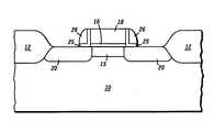
図1は、本発明の実施例の作成の初期段階の拡大断面図である。好ましくはシリコンによって構成される半導体材料10が設けられる。半導体材料10内のMOS装置の形成が説明されるが、以下の発明の処理段階をいくつか利用してバイポーラ装置を作成することもできる。一般に、MOS装置の形成は当技術では周知であるので簡単に説明する。
【0006】
まず、電界酸化層12が半導体材料10上に形成される。次に、チャネル領域15が、電界酸化層12をマスクとして用いて能動領域内に形成される。ゲート誘電層16が、半導体材料10の一部の上に形成される。次に、通常は多結晶シリコンにより構成されるゲート層18が、ゲート誘電層16上に形成され、パターニングされる。ソースおよびドレイン領域20が、ゲート層18と電界酸化層12とをマスクとして利用して形成される。
【0007】
図2は、さらに処理が進んだ図1の構造を示す。まず、ゲート誘電層16の被露出部分が除去される。次に、アルミニウムで構成される誘電層25が図2の構造上に形成される。本発明では、アルミニウムにより構成される誘電層(上記および以下に言及される)は、窒化アルミニウムまたは酸化アルミニウムにより構成される。アルミニウムからなる誘電層25は、好ましくは、アルゴンおよび窒素ガスまたは酸素ガスを用いるアルミニウムの反応性スパタリングにより形成される。金属有機化学蒸着などのその他の工程を用いてもよい。好適な実施例においては、アルミニウムからなる誘電層25は、100ないし1000オングストロームの厚みをもつ。この下限は、層をもっと薄くした場合に起こるピンホールの形成を避けようとするために設定される。ピンホールが起こると、誘電層25がそのエッチング・ストップ性を失ってしまう。また、上限は、スペーサ26(下記に説明)を形成中のアンダーカットにより寸法の制御を失わないように設定される。誘電層25の厚みは、約300ないし500オングストロームの範囲とし、エッチング・ストップ性とエッチングの容易性を両方とも最適にすることが最も好ましい。誘電層25は、犠牲エッチング・ストップ層として動作する。これについては、下記にさらに詳しく説明する。
【0008】
次に、シリコンからなる誘電層が、アルミニウムからなる誘電層25の上に形成され、過フッ化炭化水素プラズマを用いて異方性エッチングが行われ、誘電層をエッチングしてゲート層18に隣接してスペーサ26が形成される。スペーサ26は、二酸化シリコンまたは窒化シリコンによって構成される。アルミニウムからなる誘電層25は、エッチング・ストップとして機能して、ソースおよびドレイン領域20を過フッ化炭化水素プラズマへの被爆から保護する。誘電層の厚みは、スペーサ26の所望の幅により決まる。
【0009】
ソースおよびドレイン領域20に対する損傷は、アルミニウムからなる誘電層25をエッチング・ストップ層として利用することにより防止される。アルミニウムからなる誘電層25は、過フッ化炭化水素をベースにしたプラズマ・エッチングにより実質的なエッチングを受けない。窒化アルミニウム層25がないと、スペーサ26を形成するために行われるオーバーエッチングにより、ソースおよびドレイン領域20内の半導体材料10の表面が損傷を受けた。この損傷により、MOS装置の電気特性が悪くなった。
【0010】
図3は、さらに処理が進んだ図2の構造を示す。アルミニウムからなる誘電層25の被露出部分を除去するために、水酸化アンモニウム溶液が用いられる。これにより、アルミニウムからなる誘電層25とスペーサ26の誘電層とからなる複合スペーサが、ゲート層18に隣接して形成される。窒化アルミニウム層25の被露出部分が除去されると、スペーサ26がマスクとして機能する。水酸化アンモニウム溶液は、ソースおよびドレイン領域20内の半導体材料の表面を損傷しないので、電気特性の優れた装置が形成される。
【0011】
図4は、さらに処理が進んだ図3の構造を示す。まず、ケイ化物過程を用いて、ゲート層18上にケイ化物領域30が、ソースおよびドレイン領域20内にケイ化物領域31が形成される。ケイ化物過程は、当技術では周知のものである。アルミニウムからなる誘電層34が、図4の構造の表面上に形成される。アルミニウムからなる誘電層34は、好ましくは、アルミニウムからなる誘電層25に関して開示されたのと同様に形成される。次に、誘電層35がアルミニウムからなる誘電層34の表面上に形成される。誘電層35は、好ましくは、ドーピングされた二酸化シリコンからなる。アルミニウムからなる誘電層25をエッチングしてスペーサ26を形成するために上記に開示されたのと同じエッチング過程を用いて、ビア36が誘電層35およびアルミニウムからなる誘電層34内に形成される。アルミニウムからなる誘電層34もまた、本発明のこの部分内でエッチング・ストップとして機能し、下部の半導体材料10に対する損傷を防ぐ。
【0012】
図5は、さらに処理が進んだ図4の構造を示す。誘電層35上およびビア36内に金属相互接続層または金属被覆層37が形成されて、ソースおよびドレイン領域20と接触する。金属被覆層37は、通常は、半導体材料10とその上に形成されたアルミニウムからなる金属とに接触する境界金属層(別に図示せず)によって構成される。金属からなるキャッピング層38が、金属被覆層37上に形成されて、金属被覆層37の信頼性を高める。キャッピング層38は、電気泳動抵抗を高め、金属相互接続層の応力誘導による空隙形成を防ぐために用いられる。本実施例においては、キャッピング層38は、チタン・タングステンまたは窒化チタンから構成され、約125オングストロームの厚みを有する。
【0013】
多層金属被覆が形成される場合には、金属被覆層37とキャッピング層38の一部を従来のエッチングを用いて除去し、金属被覆層37とキャッピング層38の一部分だけが誘電層35上とビア36内とに残って、ソースおよびドレイン領域20に対する電気接触部を形成するようにしてもよい。
【0014】
次に、アルミニウムからなる誘電層39がキャッピング層38および誘電層35の表面上に形成される。アルミニウムからなる誘電層39は、好ましくは、アルミニウムからなる誘電層25に関して上記に開示されたのと同様に形成される。次に、誘電層40が形成およびパターニングされて、アルミニウムからなる誘電層39を露出させ、ビア42を形成する。誘電層40は、好ましくは、二酸化シリコンまたはスピン・オン・ガラスで構成される。アルミニウムからなる誘電層39は、誘電層40のエッチング中は、エッチング・ストップとして機能する。
【0015】
その後、アルミニウムからなる誘電層39は、上記に開示されたように水酸化アンモニウム・エッチングを用いて除去される。水酸化アンモニウム・エッチングは、アルミニウムからなる誘電層39に対して選択的に機能し、キャッピング層38をエッチングすることはない。
【0016】
従来は、アルミニウムからなる誘電層39を用いないと、誘電層40のパターニング中にキャッピング層38がエッチングされて、ビア42が形成された。これは、キャッピング層38が薄くて、誘電層40とほぼ同じ速度でエッチングされたためである。誘電層40のオーバーエッチングが必要とされるので、キャッピング層38が全体的に同時にエッチングされることが多かった。
【0017】
そのため、信頼性を改善するためにキャッピング層38が形成されても、従来はこの目的が達成されなかった。アルミニウムからなる誘電層39を用いることで、このように、キャッピング層38の除去を防ぐことができ、高い信頼性をもって製造される装置が得られる。第2金属被覆層45が、誘電層40の表面上に形成され、ビア42を通じてキャッピング層38と接触する。
【0018】
容易に理解されるように、種々の処理段階の間に窒化アルミニウムを利用する装置により、ソースおよびドレイン領域に対する損傷を起こさず、信頼性強化層を除去せずに装置を製造することができる。特に、上部の誘電層のエッチング中に、金属相互接続層を覆うチタン・タングステンまたは窒化チタン層を除去することが、窒化アルミニウム層をエッチング・ストップとして用いることにより阻止される。工程全体を通じて、アルミニウムからなる誘電層が犠牲エッチング・ストップ層として用いられること、またアルミニウムからなる誘電層の除去しなければならない部分が高温段階に構造をさらす前に除去されることに注目することも重要である。アルミニウムからなる誘電層が過フッ化炭化水素をベースにしたエッチング剤にさらされた後であって除去される前に高温段階が実行されると、既知の従来のエッチング剤を用いては除去することが不可能になることがわかっている。
【図面の簡単な説明】
【図1】本発明の実施例の作成の初期段階の拡大断面図である。
【図2】本発明の実施例の作成の中間段階の拡大断面図である。
【図3】本発明の実施例の作成の中間段階の拡大断面図である。
【図4】本発明の実施例の作成の中間段階の拡大断面図である。
【図5】本発明の実施例の作成の最終段階の拡大断面図である。
【符号の説明】
10 半導体材料
12 電界酸化層
15 チャネル領域
16 ゲート誘電層
18 ゲート層
20 ソースおよびドレイン領域
25,34,39 アルミニウム誘電層
26 スペーサ
30,31 ケイ化物領域
35,40 誘電層
37,45 金属被覆層
38 キャッピング層[0001]
[Industrial application fields]
The present invention generally relates to semiconductor devices, and more particularly, to a semiconductor device using an insulating layer made of aluminum, a manufacturing method thereof, and the like.
[0002]
[Background Art and Problems to be Solved by the Invention]
Silicon dioxide is usually used above the semiconductor material. In forming a small geometry, reactive ion etching is used to remove portions of the silicon dioxide layer. As the device becomes smaller, it becomes more difficult to maintain uniform etching of the silicon dioxide layer across the wafer without etching the underlying semiconductor material. This causes reactive ion etching induced damage to the surface of the semiconductor material. This damage to the surface of the semiconductor material degrades the device yield and degrades the electrical characteristics and performance of the semiconductor device.
[0003]
Another problem in etching silicon dioxide using high power RIE occurs when forming a metallization layer. Usually, a capping layer is formed on the metal coating layer in order to increase reliability. However, during the formation of vias in the silicon dioxide layer overlying the capping layer, the capping layer was also etched by high power RIE. Therefore, the capping layer is removed from the desired position of the semiconductor device, and a device with poor reliability is produced.
[0004]
Therefore, it is desirable to have a manufacturing process that can create a semiconductor device that improves reliability without etching the desired layer and without being damaged by reactive ion etching.
[0005]
【Example】
FIG. 1 is an enlarged cross-sectional view of an initial stage of creation of an embodiment of the present invention. A
[0006]
First, the
[0007]
FIG. 2 shows the structure of FIG. 1 with further processing. First, the exposed portion of the gate
[0008]
Next, a dielectric layer made of silicon is formed on the
[0009]
Damage to the source and
[0010]
FIG. 3 shows the structure of FIG. 2 with further processing. In order to remove the exposed portion of the
[0011]
FIG. 4 shows the structure of FIG. 3 with further processing. First, a
[0012]
FIG. 5 shows the structure of FIG. 4 with further processing. A metal interconnect or
[0013]
If a multi-layer metallization is formed, the
[0014]
Next, a
[0015]
Thereafter, the
[0016]
Conventionally, if the
[0017]
Therefore, even if the
[0018]
As will be readily appreciated, devices utilizing aluminum nitride during various processing steps can be fabricated without causing damage to the source and drain regions and without removing the reliability enhancement layer. In particular, removal of the titanium tungsten or titanium nitride layer covering the metal interconnect layer during etching of the upper dielectric layer is prevented by using the aluminum nitride layer as an etch stop. Note that throughout the process, an aluminum dielectric layer is used as a sacrificial etch stop layer and that the portion of the aluminum dielectric layer that must be removed is removed before exposing the structure to the high temperature stage. It is also important. If the high temperature step is performed after the aluminum dielectric layer has been exposed to the fluorocarbon based etchant and before it is removed, it is removed using known conventional etchants. I know it will be impossible.
[Brief description of the drawings]
FIG. 1 is an enlarged cross-sectional view of an initial stage of creation of an embodiment of the present invention.
FIG. 2 is an enlarged cross-sectional view of an intermediate stage of creation of an embodiment of the present invention.
FIG. 3 is an enlarged cross-sectional view of an intermediate stage of creation of an embodiment of the present invention.
FIG. 4 is an enlarged cross-sectional view of an intermediate stage of creation of an embodiment of the present invention.
FIG. 5 is an enlarged cross-sectional view of the final stage of creation of an embodiment of the present invention.
[Explanation of symbols]
10
Claims (2)
Translated fromJapanese半導体材料(10)を設ける段階;
前記半導体材料上に第1金属被覆層(37)を形成する段階;
前記第1金属被覆層上に窒化チタンまたはチタンタングステンからなる層(38)を形成する段階;
前記窒化チタンまたはチタンタングステンからなる層(38)上に窒化アルミニウムからなる誘電層(39)を形成する段階;
窒化アルミニウムからなる前記誘電層(39)上に二酸化シリコンからなる誘電層(40)を形成する段階;
窒化アルミニウムからなる前記誘電層(39)上の二酸化シリコンからなる前記誘電層(40)の一部を、窒化アルミニウムからなる前記誘電層(39)の表面が露出するまで、過フッ化炭化水素プラズマを用いた異方性エッチングにより除去し、ビア(42)を形成する段階;
前記窒化チタンまたはチタンタングステンからなる層(38)上の露出された窒化アルミニウムからなる前記誘電層(39)の一部を、前記窒化チタンまたはチタンタングステンからなる層(38)の表面が露出するまで、水酸化アンモニウム溶液により除去する段階;および
二酸化シリコンからなる前記誘電層(40)上、および前記窒化チタンまたはチタンタングステンからなる層(38)上、および前記ビア(42)内に第2金属被覆層(45)を形成する段階;
によって構成されることを特徴とする方法。A method of forming a semiconductor structure comprising:
Providing a semiconductor material (10);
Forming a first metal coating layer (37) on the semiconductor material;
Forming alayer (38) oftitanium nitride or titanium tungsten on the first metal coating layer;
Forming a dielectric layer (39) made of aluminum nitride on thelayer (38) made of titanium nitride or titanium tungsten ;
Forming a dielectric layer (40) made of silicondioxide on the dielectric layer (39) made of aluminum nitride;
The dielectric layer made of aluminum nitride (39) said dielectric layer of silicondioxide on the part of(40), to the surface of the dielectric layer made of aluminum nitride (39) is exposed, fluorocarbon plasma Removingbyanisotropic etching using ato form avia (42) ;
Part of theexposed dielectric layer (39) made of aluminum nitride on thelayer (38) made oftitanium nitride or titanium tungsten is exposed until the surface of the layer (38) made of titanium nitride or titanium tungsten is exposed. , step is removedby ammonium hydroxidesolution;Contact and
Forming a second metallization layer (45)on the dielectric layer (40) comprising silicon dioxide and on the layer (38) comprising titanium nitride or titanium tungstenand in the via (42) ;
A method characterized by comprising.
半導体材料(10)を設ける段階;
前記半導体材料(10)の部分の上にゲート層(18)を形成する段階;
前記ゲート層(18)の下の前記半導体材料(10)の部分内にチャネル領域(15)を形成する段階;
前記チャネル領域(15)に隣接する前記半導体材料(10)の部分内にソース領域(20)およびドレイン領域(20)を形成する段階;
前記半導体材料(10)上の前記ゲート層(18)に隣接してスペーサ(25,26)を形成する段階であって、
前記半導体材料(10)と前記ゲート層(18)との上に窒化アルミニウムからなる第1誘電層(25)を形成し、
窒化アルミニウムからなる前記第1誘電層(25)上に第1二酸化シリコン層(26)を形成し、そして、
前記第1二酸化シリコン層(26)の一部を、過フッ化炭化水素プラズマを用いた異方性エッチングにより除去し、窒化アルミニウムからなる前記第1誘電層(25)の一部を、水酸化アンモニウム溶液により除去して、窒化アルミニウムからなる前記第1誘電層(25)と前記第1二酸化シリコン層(26)とから構成される前記スペーサ(25,26)を形成する段階;
前記ソース領域(20)および前記ドレイン領域(20)上と、前記スペーサ(25,26)および前記ゲート層(18)上との前記半導体材料(10)の部分上に、窒化アルミニウムからなる第2誘電層(34)を形成する段階;
窒化アルミニウムからなる前記第2誘電層(34)上に第2二酸化シリコン層(35)を形成する段階;
前記ソース領域(20)の一部と前記ドレイン領域(20)の一部との上の前記第2二酸化シリコン層(35)の部分を、過フッ化炭化水素プラズマを用いた異方性エッチングにより除去する段階;
前記ソース領域(20)の一部と前記ドレイン領域(20)の一部との上の窒化アルミニウムからなる前記第2誘電層(34)の部分を、水酸化アンモニウム溶液により除去し、第1のビア(36)を形成する段階;
前記第1のビア(36)内に第1金属被覆層(37)を形成して、前記ソース領域(20)および前記ドレイン領域(20)との電気接触を行う段階;
前記第1金属被覆層上に窒化チタンまたはチタンタングステンからなる層(38)を形成する段階;
前記窒化チタンまたはチタンタングステンからなる層(38)上に窒化アルミニウムからなる第3誘電層(39)を形成する段階;
窒化アルミニウムからなる前記第3誘電層(39)上に、第3二酸化シリコン層(40)を形成する段階;
窒化アルミニウムからなる前記第3誘電層(39)をエッチング・ストップとして用いて、前記窒化チタンまたはチタンタングステンからなる層(38)上の前記第3二酸化シリコン層(40)の部分を、過フッ化炭化水素プラズマを用いた異方性エッチングにより除去する段階;
前記窒化チタンまたはチタンタングステンからなる層(38)上の、窒化アルミニウムからなる前記第3誘電層(39)の部分を、水酸化アンモニウム溶液により除去する段階であって、窒化アルミニウムからなる前記第3誘電層(39)の部分が除去され、第2のビア(42)が形成される段階;および
前記窒化チタンまたはチタンタングステンからなる層(38)上の前記第2のビア(42)内に第2金属被覆層(45)を形成する段階;
によって構成されることを特徴とする方法。A method of forming a semiconductor structure comprising:
Providing a semiconductor material (10);
Forming a gate layer (18) over the portion of the semiconductor material (10);
Forming a channel region (15) in a portion of the semiconductor material (10) under the gate layer (18);
Forming a source region (20) and a drain region (20) in a portion of the semiconductor material (10) adjacent to the channel region (15);
Forming spacers (25, 26 ) adjacent to the gate layer (18) on the semiconductor material (10),
Forming a first dielectric layer (25) made of aluminum nitride on the semiconductor material (10) and the gate layer (18);
Forming a first silicon dioxide layer (26) on said first dielectric layer (25) of aluminum nitride; and
A part of the first silicon dioxide layer (26) is removed by anisotropic etching using a fluorocarbon plasma, and a part of the first dielectric layer (25) made of aluminum nitride is hydroxylated. Removing the aluminum solution to form the spacers (25, 26) composed of the first dielectric layer (25) made of aluminum nitride and the first silicon dioxide layer (26);
A second layer of aluminumnitride is formed on the semiconductor material (10) on the source region (20) and the drain region (20) and on the spacers (25, 26) and the gate layer (18). Forming a dielectric layer (34);
Forming a second silicon dioxide layer (35) on the second dielectric layer (34) of aluminumnitride ;
A portion of the second silicon dioxide layer (35) over a portion ofthe source region (20) and a portion of the drain region (20) issubjected to anisotropic etching using a fluorocarbon plasma. Removing;
A portion of the second dielectric layer (34) made of aluminumnitride on a portion of the source region (20) and a portion of the drain region (20) is removedwith anammonium hydroxide solution, Forming avia (36) ;
Forming a first metal cover layer (37)in the firstvia (36) and making electrical contact with the source region (20) and the drain region (20);
Forming alayer (38) oftitanium nitride or titanium tungsten on the first metal coating layer;
Forming a third dielectric layer (39) made of aluminumnitride on thelayer (38) made oftitanium nitride or titanium tungsten ;
Forming a third silicon dioxide layer (40) on the third dielectric layer (39) of aluminumnitride ;
Using the third dielectric layer (39) made of aluminum nitride as an etching stop, the portion of the third silicon dioxide layer (40) on thelayer (38) made oftitanium nitride or titanium tungsten isperfluorinated. Removing byanisotropic etching using hydrocarbon plasma ;
The third dielectric layer (39) made of aluminum nitride on thelayer (38) made oftitanium nitride or titanium tungsten is removed withan ammonium hydroxide solution, and the third dielectric layer (39) is made of aluminum nitride. portions of the dielectric layer (39)isdivided,the second stagevia (42) Ruisformed;Contact and
Forming a second metal coating layer (45) in the secondvia (42) onthetitanium nitride or titanium tungsten layer (38);
A method characterized by comprising.
Applications Claiming Priority (2)
| Application Number | Priority Date | Filing Date | Title |
|---|---|---|---|
| US26834594A | 1994-06-29 | 1994-06-29 | |
| US268345 | 1994-06-29 |
Publications (2)
| Publication Number | Publication Date |
|---|---|
| JPH0817930A JPH0817930A (en) | 1996-01-19 |
| JP4417439B2true JP4417439B2 (en) | 2010-02-17 |
Family
ID=23022559
Family Applications (1)
| Application Number | Title | Priority Date | Filing Date |
|---|---|---|---|
| JP17389795AExpired - Fee RelatedJP4417439B2 (en) | 1994-06-29 | 1995-06-19 | Semiconductor device structure and method using etching stop layer |
Country Status (2)
| Country | Link |
|---|---|
| US (1) | US5707901A (en) |
| JP (1) | JP4417439B2 (en) |
Cited By (2)
| Publication number | Priority date | Publication date | Assignee | Title |
|---|---|---|---|---|
| CN109300790A (en)* | 2017-07-24 | 2019-02-01 | 格芯公司 | Contact etch stop layer with sacrificial polysilicon layer |
| TWI707396B (en)* | 2016-05-10 | 2020-10-11 | 日商東京威力科創股份有限公司 | Etching method |
Families Citing this family (22)
| Publication number | Priority date | Publication date | Assignee | Title |
|---|---|---|---|---|
| US6077763A (en)* | 1996-11-19 | 2000-06-20 | United Microelectronics Corp. | Process for fabricating a self-aligned contact |
| US5817562A (en)* | 1997-01-24 | 1998-10-06 | Taiwan Semiconductor Manufacturing Company, Ltd | Method for making improved polysilicon FET gate electrode structures and sidewall spacers for more reliable self-aligned contacts (SAC) |
| TW399266B (en)* | 1997-02-04 | 2000-07-21 | Winbond Electronics Corp | Method for etching contact windows |
| US6063698A (en)* | 1997-06-30 | 2000-05-16 | Motorola, Inc. | Method for manufacturing a high dielectric constant gate oxide for use in semiconductor integrated circuits |
| US5955380A (en)* | 1997-09-30 | 1999-09-21 | Siemens Aktiengesellschaft | Endpoint detection method and apparatus |
| US6133139A (en) | 1997-10-08 | 2000-10-17 | International Business Machines Corporation | Self-aligned composite insulator with sub-half-micron multilevel high density electrical interconnections and process thereof |
| US6846739B1 (en)* | 1998-02-27 | 2005-01-25 | Micron Technology, Inc. | MOCVD process using ozone as a reactant to deposit a metal oxide barrier layer |
| US6162722A (en)* | 1999-05-17 | 2000-12-19 | United Microelectronics Corp. | Unlanded via process |
| KR100540246B1 (en)* | 1999-12-22 | 2006-01-12 | 주식회사 하이닉스반도체 | Manufacturing Method of Semiconductor Device |
| US6537902B1 (en)* | 2000-01-24 | 2003-03-25 | Oki Electric Industry Co, Ltd. | Method of forming a via hole in a semiconductor device |
| US6306313B1 (en) | 2000-02-04 | 2001-10-23 | Agere Systems Guardian Corp. | Selective etching of thin films |
| US6251796B1 (en)* | 2000-02-24 | 2001-06-26 | Conexant Systems, Inc. | Method for fabrication of ceramic tantalum nitride and improved structures based thereon |
| US6734071B1 (en)* | 2000-08-30 | 2004-05-11 | Micron Technology, Inc. | Methods of forming insulative material against conductive structures |
| KR100400035B1 (en)* | 2001-02-21 | 2003-09-29 | 삼성전자주식회사 | Semiconductor device with contacts having uniform contact resistance and method for manufacturing the same |
| US6949481B1 (en) | 2003-12-09 | 2005-09-27 | Fasl, Llc | Process for fabrication of spacer layer with reduced hydrogen content in semiconductor device |
| US6955965B1 (en) | 2003-12-09 | 2005-10-18 | Fasl, Llc | Process for fabrication of nitride layer with reduced hydrogen content in ONO structure in semiconductor device |
| KR100540341B1 (en)* | 2003-12-31 | 2006-01-11 | 동부아남반도체 주식회사 | Semiconductor device manufacturing method |
| US7196008B1 (en)* | 2005-03-23 | 2007-03-27 | Spansion Llc | Aluminum oxide as liner or cover layer to spacers in memory device |
| JP2009016754A (en)* | 2007-07-09 | 2009-01-22 | Toshiba Corp | Semiconductor device and manufacturing method thereof |
| JP5816570B2 (en)* | 2011-05-27 | 2015-11-18 | ルネサスエレクトロニクス株式会社 | Semiconductor device manufacturing method and semiconductor device |
| US10355131B2 (en)* | 2016-05-17 | 2019-07-16 | Taiwan Semiconductor Manufacturing Company Ltd. | Semiconductor structure and manufacturing method thereof |
| US10755972B2 (en)* | 2016-11-29 | 2020-08-25 | Taiwan Semiconductor Manufacturing Company, Ltd. | Semiconductor device and method |
Family Cites Families (17)
| Publication number | Priority date | Publication date | Assignee | Title |
|---|---|---|---|---|
| JPS60136267A (en)* | 1983-12-23 | 1985-07-19 | Fujitsu Ltd | Manufacture of semiconductor device |
| US4944836A (en)* | 1985-10-28 | 1990-07-31 | International Business Machines Corporation | Chem-mech polishing method for producing coplanar metal/insulator films on a substrate |
| US4789648A (en)* | 1985-10-28 | 1988-12-06 | International Business Machines Corporation | Method for producing coplanar multi-level metal/insulator films on a substrate and for forming patterned conductive lines simultaneously with stud vias |
| JPS62272571A (en)* | 1986-05-21 | 1987-11-26 | Hitachi Ltd | Semiconductor device |
| JPS62276832A (en)* | 1986-05-26 | 1987-12-01 | Hitachi Ltd | Method of forming film and manufacture of semiconductor device employing the same |
| US4824803A (en)* | 1987-06-22 | 1989-04-25 | Standard Microsystems Corporation | Multilayer metallization method for integrated circuits |
| JPH0626201B2 (en)* | 1987-10-15 | 1994-04-06 | 富士通株式会社 | Method for manufacturing semiconductor device |
| US5001076A (en)* | 1987-10-23 | 1991-03-19 | Vitesse Semiconductor Corporation | Process for fabricating III-V devices using a composite dielectric layer |
| US4855247A (en)* | 1988-01-19 | 1989-08-08 | Standard Microsystems Corporation | Process for fabricating self-aligned silicide lightly doped drain MOS devices |
| JPH01244666A (en)* | 1988-03-25 | 1989-09-29 | Nec Corp | Manufacture of semiconductor device |
| JPH0475351A (en)* | 1990-07-17 | 1992-03-10 | Mitsubishi Electric Corp | Method for manufacturing compound semiconductor device |
| EP0469214A1 (en)* | 1990-07-31 | 1992-02-05 | International Business Machines Corporation | Method of forming stacked conductive and/or resistive polysilicon lands in multilevel semiconductor chips and structures resulting therefrom |
| US5118382A (en)* | 1990-08-10 | 1992-06-02 | Ibm Corporation | Elimination of etch stop undercut |
| US5240871A (en)* | 1991-09-06 | 1993-08-31 | Micron Technology, Inc. | Corrugated storage contact capacitor and method for forming a corrugated storage contact capacitor |
| US5270263A (en)* | 1991-12-20 | 1993-12-14 | Micron Technology, Inc. | Process for depositing aluminum nitride (AlN) using nitrogen plasma sputtering |
| US5284549A (en)* | 1992-01-02 | 1994-02-08 | International Business Machines Corporation | Selective fluorocarbon-based RIE process utilizing a nitrogen additive |
| US5451543A (en)* | 1994-04-25 | 1995-09-19 | Motorola, Inc. | Straight sidewall profile contact opening to underlying interconnect and method for making the same |
- 1995
- 1995-06-19JPJP17389795Apatent/JP4417439B2/ennot_activeExpired - Fee Related
- 1996
- 1996-07-29USUS08/688,081patent/US5707901A/ennot_activeExpired - Fee Related
Cited By (3)
| Publication number | Priority date | Publication date | Assignee | Title |
|---|---|---|---|---|
| TWI707396B (en)* | 2016-05-10 | 2020-10-11 | 日商東京威力科創股份有限公司 | Etching method |
| CN109300790A (en)* | 2017-07-24 | 2019-02-01 | 格芯公司 | Contact etch stop layer with sacrificial polysilicon layer |
| CN109300790B (en)* | 2017-07-24 | 2021-11-02 | 格芯(美国)集成电路科技有限公司 | Contact etch stop layer with sacrificial polysilicon layer |
Also Published As
| Publication number | Publication date |
|---|---|
| US5707901A (en) | 1998-01-13 |
| JPH0817930A (en) | 1996-01-19 |
Similar Documents
| Publication | Publication Date | Title |
|---|---|---|
| JP4417439B2 (en) | Semiconductor device structure and method using etching stop layer | |
| KR100376628B1 (en) | Conductive Interconnect Structure in Integrated Circuit and Method of Forming Conductive Interconnect | |
| US5872063A (en) | Self-aligned contact structures using high selectivity etching | |
| GB2214709A (en) | A method of enabling connection to a substructure forming part of an electronic device | |
| JPH03138934A (en) | Etching of window having different depth | |
| JP3312604B2 (en) | Method for manufacturing semiconductor device | |
| US6211557B1 (en) | Contact structure using taper contact etching and polycide step | |
| US6093627A (en) | Self-aligned contact process using silicon spacers | |
| JP3959790B2 (en) | Manufacturing method of semiconductor device | |
| US6528372B2 (en) | Sidewall spacer definition of gates | |
| KR100243280B1 (en) | Gate pattern of semiconductor device &fabrication method thereof | |
| JP3449137B2 (en) | Method for manufacturing semiconductor device | |
| US20010051386A1 (en) | Method of manufacturing a semiconductor device | |
| JPH11204636A (en) | Method for manufacturing semiconductor device | |
| JPH02117153A (en) | Method of forming semiconductor element | |
| KR100191710B1 (en) | Metal wiring method of semiconductor device | |
| US6281092B1 (en) | Method for manufacturing a metal-to-metal capacitor utilizing only one masking step | |
| KR100518527B1 (en) | Manufacturing method of semiconductor device having low resistance gate electrode | |
| JPH05226333A (en) | Manufacture of semiconductor device | |
| KR100356475B1 (en) | Method of manufacturing a transistor | |
| KR100447989B1 (en) | Gate electrode formation method of semiconductor device | |
| KR100305642B1 (en) | Contact hole formation method of semiconductor device | |
| TW396455B (en) | Semiconductor process for improving non-uniform etching thickness by providing etch stop layer | |
| JPH0734440B2 (en) | Wiring forming method in semiconductor device | |
| JPH09270463A (en) | Method of forming contact holes |
Legal Events
| Date | Code | Title | Description |
|---|---|---|---|
| A711 | Notification of change in applicant | Free format text:JAPANESE INTERMEDIATE CODE: A711 Effective date:20041217 | |
| RD03 | Notification of appointment of power of attorney | Free format text:JAPANESE INTERMEDIATE CODE: A7423 Effective date:20050304 | |
| RD04 | Notification of resignation of power of attorney | Free format text:JAPANESE INTERMEDIATE CODE: A7424 Effective date:20050310 | |
| A977 | Report on retrieval | Free format text:JAPANESE INTERMEDIATE CODE: A971007 Effective date:20050427 | |
| A131 | Notification of reasons for refusal | Free format text:JAPANESE INTERMEDIATE CODE: A131 Effective date:20050506 | |
| A521 | Request for written amendment filed | Free format text:JAPANESE INTERMEDIATE CODE: A523 Effective date:20050804 | |
| A131 | Notification of reasons for refusal | Free format text:JAPANESE INTERMEDIATE CODE: A131 Effective date:20070111 | |
| A601 | Written request for extension of time | Free format text:JAPANESE INTERMEDIATE CODE: A601 Effective date:20070112 | |
| A602 | Written permission of extension of time | Free format text:JAPANESE INTERMEDIATE CODE: A602 Effective date:20070117 | |
| A521 | Request for written amendment filed | Free format text:JAPANESE INTERMEDIATE CODE: A523 Effective date:20070711 | |
| A02 | Decision of refusal | Free format text:JAPANESE INTERMEDIATE CODE: A02 Effective date:20070813 | |
| A521 | Request for written amendment filed | Free format text:JAPANESE INTERMEDIATE CODE: A523 Effective date:20071212 | |
| A911 | Transfer to examiner for re-examination before appeal (zenchi) | Free format text:JAPANESE INTERMEDIATE CODE: A911 Effective date:20071220 | |
| A912 | Re-examination (zenchi) completed and case transferred to appeal board | Free format text:JAPANESE INTERMEDIATE CODE: A912 Effective date:20080307 | |
| RD13 | Notification of appointment of power of sub attorney | Free format text:JAPANESE INTERMEDIATE CODE: A7433 Effective date:20090422 | |
| A521 | Request for written amendment filed | Free format text:JAPANESE INTERMEDIATE CODE: A821 Effective date:20090422 | |
| A601 | Written request for extension of time | Free format text:JAPANESE INTERMEDIATE CODE: A601 Effective date:20090904 | |
| A602 | Written permission of extension of time | Free format text:JAPANESE INTERMEDIATE CODE: A602 Effective date:20090909 | |
| A521 | Request for written amendment filed | Free format text:JAPANESE INTERMEDIATE CODE: A523 Effective date:20091001 | |
| A01 | Written decision to grant a patent or to grant a registration (utility model) | Free format text:JAPANESE INTERMEDIATE CODE: A01 | |
| A61 | First payment of annual fees (during grant procedure) | Free format text:JAPANESE INTERMEDIATE CODE: A61 Effective date:20091126 | |
| R150 | Certificate of patent or registration of utility model | Free format text:JAPANESE INTERMEDIATE CODE: R150 | |
| FPAY | Renewal fee payment (event date is renewal date of database) | Free format text:PAYMENT UNTIL: 20121204 Year of fee payment:3 | |
| FPAY | Renewal fee payment (event date is renewal date of database) | Free format text:PAYMENT UNTIL: 20131204 Year of fee payment:4 | |
| R250 | Receipt of annual fees | Free format text:JAPANESE INTERMEDIATE CODE: R250 | |
| LAPS | Cancellation because of no payment of annual fees |