JP4416372B2 - Semiconductor memory device - Google Patents
Semiconductor memory deviceDownload PDFInfo
- Publication number
- JP4416372B2 JP4416372B2JP2002047464AJP2002047464AJP4416372B2JP 4416372 B2JP4416372 B2JP 4416372B2JP 2002047464 AJP2002047464 AJP 2002047464AJP 2002047464 AJP2002047464 AJP 2002047464AJP 4416372 B2JP4416372 B2JP 4416372B2
- Authority
- JP
- Japan
- Prior art keywords
- refresh
- address
- thinning
- unit
- signal
- Prior art date
- Legal status (The legal status is an assumption and is not a legal conclusion. Google has not performed a legal analysis and makes no representation as to the accuracy of the status listed.)
- Expired - Fee Related
Links
Images


Classifications
- G—PHYSICS
- G11—INFORMATION STORAGE
- G11C—STATIC STORES
- G11C29/00—Checking stores for correct operation ; Subsequent repair; Testing stores during standby or offline operation
- G11C29/04—Detection or location of defective memory elements, e.g. cell constructio details, timing of test signals
- G11C29/50—Marginal testing, e.g. race, voltage or current testing
- G11C29/50016—Marginal testing, e.g. race, voltage or current testing of retention
- G—PHYSICS
- G11—INFORMATION STORAGE
- G11C—STATIC STORES
- G11C11/00—Digital stores characterised by the use of particular electric or magnetic storage elements; Storage elements therefor
- G11C11/21—Digital stores characterised by the use of particular electric or magnetic storage elements; Storage elements therefor using electric elements
- G11C11/34—Digital stores characterised by the use of particular electric or magnetic storage elements; Storage elements therefor using electric elements using semiconductor devices
- G11C11/40—Digital stores characterised by the use of particular electric or magnetic storage elements; Storage elements therefor using electric elements using semiconductor devices using transistors
- G11C11/401—Digital stores characterised by the use of particular electric or magnetic storage elements; Storage elements therefor using electric elements using semiconductor devices using transistors forming cells needing refreshing or charge regeneration, i.e. dynamic cells
- G11C11/406—Management or control of the refreshing or charge-regeneration cycles
- G11C11/40603—Arbitration, priority and concurrent access to memory cells for read/write or refresh operations
- G—PHYSICS
- G11—INFORMATION STORAGE
- G11C—STATIC STORES
- G11C29/00—Checking stores for correct operation ; Subsequent repair; Testing stores during standby or offline operation
- G11C29/02—Detection or location of defective auxiliary circuits, e.g. defective refresh counters
- G11C29/028—Detection or location of defective auxiliary circuits, e.g. defective refresh counters with adaption or trimming of parameters
- G—PHYSICS
- G11—INFORMATION STORAGE
- G11C—STATIC STORES
- G11C29/00—Checking stores for correct operation ; Subsequent repair; Testing stores during standby or offline operation
- G11C29/04—Detection or location of defective memory elements, e.g. cell constructio details, timing of test signals
- G11C29/50—Marginal testing, e.g. race, voltage or current testing
- G—PHYSICS
- G11—INFORMATION STORAGE
- G11C—STATIC STORES
- G11C29/00—Checking stores for correct operation ; Subsequent repair; Testing stores during standby or offline operation
- G11C29/70—Masking faults in memories by using spares or by reconfiguring
- G11C29/78—Masking faults in memories by using spares or by reconfiguring using programmable devices
- G11C29/783—Masking faults in memories by using spares or by reconfiguring using programmable devices with refresh of replacement cells, e.g. in DRAMs
- G—PHYSICS
- G11—INFORMATION STORAGE
- G11C—STATIC STORES
- G11C8/00—Arrangements for selecting an address in a digital store
- G11C8/18—Address timing or clocking circuits; Address control signal generation or management, e.g. for row address strobe [RAS] or column address strobe [CAS] signals
- G—PHYSICS
- G11—INFORMATION STORAGE
- G11C—STATIC STORES
- G11C11/00—Digital stores characterised by the use of particular electric or magnetic storage elements; Storage elements therefor
- G11C11/21—Digital stores characterised by the use of particular electric or magnetic storage elements; Storage elements therefor using electric elements
- G11C11/34—Digital stores characterised by the use of particular electric or magnetic storage elements; Storage elements therefor using electric elements using semiconductor devices
- G11C11/40—Digital stores characterised by the use of particular electric or magnetic storage elements; Storage elements therefor using electric elements using semiconductor devices using transistors
- G11C11/401—Digital stores characterised by the use of particular electric or magnetic storage elements; Storage elements therefor using electric elements using semiconductor devices using transistors forming cells needing refreshing or charge regeneration, i.e. dynamic cells
- G—PHYSICS
- G11—INFORMATION STORAGE
- G11C—STATIC STORES
- G11C2207/00—Indexing scheme relating to arrangements for writing information into, or reading information out from, a digital store
- G11C2207/22—Control and timing of internal memory operations
- G11C2207/2227—Standby or low power modes
- G—PHYSICS
- G11—INFORMATION STORAGE
- G11C—STATIC STORES
- G11C2211/00—Indexing scheme relating to digital stores characterized by the use of particular electric or magnetic storage elements; Storage elements therefor
- G11C2211/401—Indexing scheme relating to cells needing refreshing or charge regeneration, i.e. dynamic cells
- G11C2211/406—Refreshing of dynamic cells
- G11C2211/4061—Calibration or ate or cycle tuning
- G—PHYSICS
- G11—INFORMATION STORAGE
- G11C—STATIC STORES
- G11C2211/00—Indexing scheme relating to digital stores characterized by the use of particular electric or magnetic storage elements; Storage elements therefor
- G11C2211/401—Indexing scheme relating to cells needing refreshing or charge regeneration, i.e. dynamic cells
- G11C2211/406—Refreshing of dynamic cells
- G11C2211/4067—Refresh in standby or low power modes
Landscapes
- Engineering & Computer Science (AREA)
- Microelectronics & Electronic Packaging (AREA)
- Computer Hardware Design (AREA)
- Dram (AREA)
Description
Translated fromJapanese【0001】
【発明の属する技術分野】
本発明は、半導体記憶装置に関するものであり、特に、スタンバイ状態における消費電流の低減に関するものである。
【0002】
【従来の技術】
リフレッシュ動作が必要な半導体記憶装置では、低消費電流動作が求められるスタンバイ時においても定期的にリフレッシュ動作を行なわなければならず、リフレッシュ動作における消費電流の低減が必須となっている。
【0003】
一般的に、半導体記憶装置に搭載されている記憶セルは、記憶されているデータの保持特性に一定の幅を有している。そのため、同一記憶セルがリフレッシュされる時間間隔であるリフレッシュ周期tREFは、データ保持特性の最悪値に対して設定されなければならないところ、より良好なデータ保持特性を有する記憶セルについては、設定されたリフレッシュ周期tREFよりも長い周期でリフレッシュ動作をしてやれば充分である。そこで、良好なデータ保持特性を有する記憶セルに対してはリフレッシュ周期tREFの2周期以上ごとに1回のリフレッシュ動作を行なう、いわゆる間引きリフレッシュ動作が提案されている。これにより、所定時間あたりのリフレッシュ動作回数が減少し、リフレッシュ動作時における消費電流を低減することができる。
【0004】
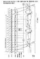
特開平9−102193号公報には、間引きリフレッシュ機能を有する半導体記憶装置が開示されている。図24には、主にロウアドレス系の回路構成を示す。/CASビフォア/RAS(以下、CBRと略記する)リフレッシュ動作に間引きリフレッシュ機能を備える場合を例示している。
【0005】
タイミング回路131は、制御端子101に与えられる制御信号に従って、ロウアドレスデコーダ137を活性化させるための活性化信号φRのトリガ信号を所定のタイミングで出力する。このトリガ信号は、アンド論理ゲート400bに入力される。また、後述の間引きリフレッシュ制御回路105を活性化する活性化信号φ1を出力する。
【0006】
ロウアドレスバッファ132は、アドレス端子101に与えられるアドレス信号を制御信号/RASの立下がり時刻でラッチし、ラッチしたアドレス信号をロウアドレスAdd(O)としてアドレスセレクタ135に与える。
【0007】
CBR判定回路133は、CBRリフレッシュモードの設定が行なわれたことに応じて、リフレッシュ指示信号φCBRを出力する。
【0008】
CBRカウンタ134は、リフレッシュ指示信号φCBRの立下がりをカウントしてリフレッシュアドレスAdd(C)をアドレスセレクタ135に出力する。
【0009】
アドレスセレクタ135は、リフレッシュ指示信号φCBRによって制御され、読出および書込動作時はロウアドレスバッファ132とロウアドレスデコーダ137とを結合し、リフレッシュ動作時はCBRカウンタ134とロウアドレスデコーダ137とを結合する。
【0010】
活性化信号φ1で活性化された間引きリフレッシュ制御回路105には、CBRカウンタ134から出力されるリフレッシュアドレスAdd(C)が入力されており、このアドレスAdd(C)が登録されたアドレスであるか否かの判定が行なわれる。判定結果に応じてリフレッシュ許可信号φ2をアンド論理ゲート400bの他方の入力端子に出力し、活性化信号φRの出力を制御する。
【0011】
ロウアドレスデコーダ137は、活性化信号φRによって活性化され、アドレスセレクタ135を介して入力されるロウアドレスAdd(O)またはリフレッシュアドレスAdd(C)に従って、メモリセルアレイ140の複数のワード線(WL0〜WLn)のうちの何れか1本をワードドライバ104により活性化する。
【0012】
すなわち、通常の書込/読出サイクルにおいては、制御信号/RASは制御信号/CASよりも先に立下がるので、CBR判定回路133の出力信号φCBRは非活性化レベルに保持される。そのため、アドレスセレクタ135は、ロウアドレスバッファ132から出力されたロウアドレスAdd(O)をロウアドレスデコーダ137に出力する。その後、タイミング回路131で生成された活性化信号φRによってロウアドレスデコーダ137が活性化され、書込/読出サイクルに応じたワード線が活性化される。
【0013】
CBRリフレッシュサイクルにおいては、制御信号/CASは制御信号/RASよりも先に立下がるので、CBR判定回路133の出力信号φCBRは活性化レベルとなる。そのため、アドレスセレクタ135は、CBRカウンタ134から出力されるリフレッシュアドレスAdd(C)をロウアドレスデコーダ137に出力する。このとき、リフレッシュアドレスAdd(C)と登録アドレスとが一致した場合には、許可信号φ2が活性化され、活性化信号φRがロウアドレスデコーダ137に与えられ、リフレッシュアドレスAdd(C)に応じたワード線が活性化される。一致しない場合には、活性化信号φRはマスクされワード線は活性化されない。
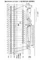
【0014】
図25には、間引きリフレッシュ制御回路105を中心に回路図を示している。CBRカウンタ134から出力されるリフレッシュアドレスAdd(C)を構成するn+1ビット内部アドレス信号A0'〜An'およびその反転信号/A0'〜/An'は、アドレス登録回路1.1〜1.rに入力される。
【0015】
各アドレス登録回路1.1〜1.rは、NMOSトランジスタ600と、アドレス信号A0'〜An'およびその反転信号/A0'〜/An'の各々に対応して設けられた、ヒューズ7.0〜7.nおよびNMOSトランジスタ8.0〜8.nと、ヒューズ7.0'〜7.n'およびNMOSトランジスタ8.0'〜8.n'とが備えられている。
【0016】
リフレッシュアドレスAdd(C)が、アドレス登録回路1.1〜1.rに登録されたアドレスのうち何れかに一致する場合には、アドレス登録回路1.1〜1.rの出力φH1〜φHrのうちの何れかの信号がハイレベルとなり、リフレッシュ許可信号φ2がハイレベルとなる。
【0017】
また、近年、携帯機器の普及に伴い機器に要求される機能が増大してきた結果、従来から搭載されていたスタティックランダムアクセスメモリ(以下、SRAM)に代えて、更に大容量のメモリが要求されるに至っている。これを限られたスペースに現実的な価格で実装する必要から、SRAMの記憶セルに代えて高集積でビット単価の安いダイナミックランダムアクセスメモリ(以下、DRAM)の記憶セルを使用しながら、DRAM等の記憶セルに特有なリフレッシュ動作に関する制御を内蔵する、いわゆる擬似SRAMといわれるリフレッシュ機能内蔵のDRAMが使用されてきている。これにより、外部のコントローラは、外部アクセスがない期間にセルフリフレッシュコマンドやセルフリフレッシュ動作を行なわせるための制御信号を出力してやれば、リフレッシュアドレスの制御等は擬似SRAM自身が行なう、いわゆるセルフリフレッシュモードを搭載してきている。また、今後の高速化要求に対して、同期型のSRAM(以下、SSRAM)の外部仕様に適合した、いわゆる擬似SSRAMなる仕様も現実的なものになりつつある。
【0018】
【発明が解決しようとする課題】
しかしながら、特開平9−102193号公報に例示される間引きリフレッシュ機能を有する半導体記憶装置では、アドレス登録回路1.1〜1.rにより、リフレッシュ周期tREFごとにリフレッシュを行なう必要のあるロウアドレスを登録する必要があり、ロウアドレスごとにアドレス登録回路1.1〜1.rが必要となる。更に、各アドレス登録回路1.1〜1.rには、ロウアドレスのビット幅分のヒューズが必要である。すなわち、半導体記憶装置に搭載しなければならないヒューズの総数は、(ロウアドレスのビット幅)×(毎周期リフレッシュを行なうべきロウアドレス数)が必要となる。半導体記憶装置におけるデータ保持特性の分布に対してリフレッシュ動作による消費電流の有効な低減効果を得るためには、多数のヒューズを備えねばならず、半導体記憶装置のダイサイズの増大を招くおそれがあり問題である。
【0019】
また、アドレス登録回路1.1〜1.rにアドレスを登録する際、多数のヒューズをカットするため、多大な試験時間が必要となる。更に、リフレッシュアドレスAdd(C)が内蔵のカウンタにより生成され外部からの制御には制約があること、また、特性不良セルを置き換えるための冗長領域に対する間引きリフレッシュ制御の設定等においても、機能試験を実施するにあたり多大な試験時間を必要とする場合も想定され、問題である。
【0020】
また、リフレッシュアドレスAdd(C)は、ロウアドレスバッファ137に加え間引きリフレッシュ制御回路105にも接続されるため、CBRカウンタ134は、これらの負荷を駆動しなければならず駆動電流の増大を招くおそれがある。また、間引きリフレッシュ制御回路105は、リフレッシュ動作の実行判定の如何に関わらずリフレッシュアドレスAdd(C)と登録されたアドレスとの比較を常時行なう構成であるため、判定動作が必要とされない期間においても不要な消費電流が流れてしまう。これらの消費電流により低消費電流の要請に応えることができないおそれがあり問題である。特に、スタンバイ時においては、元々の消費電流値自体が小さいため、総消費電流に占める間引きリフレッシュ制御回路105の動作電流の割合は大きなものとなり、低消費電流化にとって問題である。
【0021】
また、従来、擬似SRAMあるいは擬似SSRAMと称せられている半導体記憶装置では、リフレッシュ動作のための外部コントローラの負荷が大幅に軽減されてはいるものの、外部コントローラによる制御は依然として必要である。また制御にあたって、専用の制御端子を備える必要のある場合もある。そのため、従来の擬似SRAM等では、本来このような制御または制御端子が不要なSRAMあるいはSSRAMとは完全な互換性を有しているとは言い難い。そこで、この互換性をより完全なものに近づけるため、リフレッシュ動作を内部アクセス動作として内蔵しながら、リフレッシュ動作と、外部アクセス動作である通常のデータ読み出し・書き込み動作とが互いに随時のタイミングで独立して動作する仕様を有する半導体記憶装置が提案されている。しかしながら、この半導体記憶装置に間引きリフレッシュ機能を付加した場合、間引きリフレッシュ制御回路によるリフレッシュアドレスの判定時間のため、更に、前述したリフレッシュアドレスの信号経路上の負荷による伝播遅延のため、リフレッシュの動作時間が長くなってしまう場合があり、動作上のサイクルタイムが長くなってしまうおそれがあり問題である。
【0022】
本発明は前記従来技術の問題点を解消するためになされたものであり、従来の半導体記憶装置では不十分であった消費電流の更なる低減を図ると共に、互換性を高めた擬似SRAM等に適用しても動作上の遅延増大を招くことのない、好適な間引きリフレッシュ機能を実現することにより、スタンバイ状態での消費電流の低減を図ることが可能な半導体記憶装置を提供することを主たる目的とする。
【0023】
【課題を解決するための手段】
前記目的を達成するために、請求項1に係る半導体記憶装置は、リフレッシュ要求信号に応じて対象となるワード線を順次選択してリフレッシュ動作を行なう際、リフレッシュ動作の間引きを行なう間引きリフレッシュ制御部と、複数のリフレッシュ要求信号に基づいて対象とされるワード線群についての対応アドレスを指定する指定部とを備え、間引きリフレッシュ制御部は、リフレッシュ周期でのリフレッシュ動作が必要な第1のデータ保持特性を有する記憶セル、または、リフレッシュ周期でのリフレッシュ動作が必要でない第2のデータ保持特性を有する記憶セル、が接続されているワード線を含む所定ワード線群についての所定アドレスを予め格納する格納部と、指定部により指定される対応アドレスと、格納部に格納されている所定アドレスとを比較する比較部と、比較結果に応じて、指定部により指定される対応アドレスがリフレッシュ動作における間引き制御の対象であるか否かを判定する判定部と、記憶セルが有するデータ保持特性の分布において、第1のデータ保持特性を有する記憶セルに比して第2のデータ保持特性を有する記憶セルが多い場合には、格納部に格納すべき所定アドレスを第1のデータ保持特性を有する記憶セルを含むアドレスに、第2のデータ保持特性を有する記憶セルに比して第1のデータ保持特性を有する記憶セルが多い場合には、格納部に格納すべき所定アドレスを第2のデータ保持特性を有する記憶セルを含むアドレスに、切り替える格納切り替え部とを備え、判定部は、第1のデータ保持特性を有する記憶セルを含むアドレスが格納されている場合には、比較部による比較結果が不一致である場合に、第2のデータ保持特性を有する記憶セルを含むアドレスが格納されている場合には、比較部による比較結果が一致である場合に、対応アドレスがリフレッシュ動作における間引き制御の対象であると判定することを特徴とする。
【0024】
請求項1の半導体記憶装置では、リフレッシュ動作の間引きを行なう間引きリフレッシュ制御部が、格納部と比較部と判定部とを備えており、指定部により指定される、複数のリフレッシュ要求信号で対象とされるワード線群についての対応アドレスと、格納部に格納されている、リフレッシュ周期でのリフレッシュ動作が必要な第1のデータ保持特性を有する記憶セル、または、リフレッシュ周期でのリフレッシュ動作が必要でない第2のデータ保持特性を有する記憶セル、が接続されているワード線を含む所定ワード線群についての所定アドレスとが比較部で比較され、この比較結果に応じて、指定部により指定される対応アドレスがリフレッシュ動作における間引き制御の対象であるか否かを判定部により判定する。
また、格納切り替え部により、半導体記憶装置内の記憶セルのデータ保持特性の分布に応じて、格納部に格納すべき所定アドレスを、第1と第2のデータ保持特性との各々のデータ保持特性を有する記憶セルを含むアドレス間で切り替えるとともに、判定部により、第1のデータ保持特性を有する記憶セルを含むアドレスが格納されている場合には、比較部による比較結果が不一致である場合に、また、第2のデータ保持特性を有する記憶セルを含むアドレスが格納されている場合には、比較部による比較結果が一致である場合に、対応アドレスがリフレッシュ動作における間引き制御の対象であると判定する。
【0025】
これにより、格納部に格納するために備えられるヒューズ、ROM、RAM等は、対応アドレス群ごとに備えればよく、リフレッシュ要求信号に応じて対象となるワード線についてのアドレスごとに備える場合に比して、半導体記憶装置のダイサイズにおける格納部の占有面積を縮小することができる。
また、半導体記憶装置内の記憶セルが有するデータ保持特性の分布に応じて、格納部に格納すべき所定アドレスを切り替え、リフレッシュ動作の実行可否の判定結果を切り替えることができるので、データ保持特性の分布に合わせて、格納部に格納すべき所定アドレスの数が少なくなるように切り替えることができる。格納部に備えるべきヒューズ、ROM、RAM等の配置数を圧縮して半導体記憶装置のダイサイズの増大を抑制することができる。
また、格納すべき所定アドレスの数が圧縮されるため、格納部への所定アドレスの格納処理手続きを軽減することができる。処理時間の短縮、それに伴う処理費用の削減を図ることができる。
【0026】
ここで、リフレッシュ動作の実行可否の判定単位を対応アドレスごとにまとめるので、リフレッシュ動作の実行の必要がないワード線を含んでリフレッシュ動作の実行判定がなされる場合がある。また、逆に、個々のワード線について実行可否の判定をする設定では、ワード線についてのアドレスごとに格納部を設ける必要があり、格納部の占有面積が多大となってしまう。すなわち、格納部の占有面積と間引きリフレッシュによる消費電流の低減とは相反する関係にある。対応アドレスでまとめられるリフレッシュ要求信号の発生回数を調整することにより、間引きリフレッシュ動作による消費電流の低減を、格納部による占有面積の増大を抑制しながら実現することができる。
また、記憶セルのデータ保持特性の実力に応じて、リフレッシュ周期tREFが決定される。すなわち、データ保持特性が相対的に悪い記憶セルに対しては、より短い周期でリフレッシュ動作を行なうことが必要である。リフレッシュ周期tREFは、データ保持特性が悪い記憶セルに律速して設定されるため、データ保持特性が相対的に良好な記憶セルに対しては、リフレッシュ要求信号に応じてリフレッシュ動作の実行可否を判定して、必要に応じてリフレッシュ動作を実行してやればよい。これに対して、データ保持特性が相対的に悪い記憶セルに対しては、リフレッシュ要求信号ごとにリフレッシュ動作を実行する必要がある。
【0027】
また、請求項2の半導体記憶装置では、リフレッシュアドレスの一部に基づいて、リフレッシュ動作の対象とされるワード線群についての対応アドレスが指定されることが好ましい。
また、請求項3に係る半導体記憶装置は、請求項1または2に記載の半導体記憶装置において、指定部は、リフレッシュ動作の対象とされるワード線についての対応アドレスをデコードするロウアドレスデコーダとは別の専用デコーダを備えることを特徴とする。
【0028】
請求項3の半導体記憶装置では、指定部は、ロウアドレスデコーダとは別途に設けられた専用のデコーダにより、複数のリフレッシュ要求信号で対象とされるワード線群についての個々の対応アドレスがデコードされて対応アドレス群が指定される。
【0029】
これにより、リフレッシュ動作の実行可否の判定に必要となる対応アドレス群の指定を、専用のデコーダを備えてリフレッシュ動作の対象とされるワード線についての対応アドレスのデコードにより行なうので、リフレッシュ動作の実行可否の判定に際して、ロウアドレスデコーダの負荷が増大することはない。リフレッシュ動作の可否判定を行なわない設定の場合、または外部アクセス動作の場合に、ロウアドレスデコーダの負荷が増大することはない。リフレッシュ動作の実行可否の判定機能を導入しても、アクセス動作の負担の増大を招くことはなく、消費電流の増大やアクセス動作の遅延等が招来されることはない。
【0030】
また、対応アドレス群を、ロウアドレスデコーダとは別途に設けられた専用デコーダにより独立に指定できるので、ロウアドレスデコーダのデコード処理に制約されることはない。判定の単位としてまとめられるリフレッシュ要求信号の発生回数を自由に設定して対応アドレス群を指定することができる。リフレッシュ要求信号の発生回数の調整を的確に行なうことができ、間引きリフレッシュ動作による消費電流の低減と格納部による占有面積の増大とのバランスを図ることができる。
【0031】
また、請求項4に係る半導体記憶装置は、請求項1または2に記載の半導体記憶装置において、指定部は、リフレッシュ動作の対象とされるワード線についての対応アドレスをデコードするロウアドレスデコーダを含むことを特徴とする。
【0032】
請求項4の半導体記憶装置では、指定部は、ロウアドレスデコーダにより、複数のリフレッシュ要求信号で対象とされるワード線群についての個々の対応アドレスがデコードされて対応アドレス群が指定される。
【0033】
これにより、対応アドレス群の指定を、ロウアドレスデコーダで共用することができ、リフレッシュ動作の実行可否の判定機能を導入しても半導体記憶装置のダイサイズの増大を抑制することができる。
【0034】
【0035】
【0036】
【0037】
【0038】
【0039】
また、請求項5に係る半導体記憶装置は、請求項1乃至4の何れか一に記載の半導体記憶装置において、試験時に活性化され、判定部からの判定結果を外部に出力する出力部を備えることを特徴とする。
【0040】
請求項5の半導体記憶装置では、出力部は試験時に活性化され、間引きリフレッシュ制御部からの判定結果を外部に出力する。
【0041】
これにより、必要に応じて、間引きリフレッシュ制御部におけるリフレッシュ動作の実行可否の判定結果を外部から観測することができ、半導体記憶装置の不良解析や特性調査等に利用することができるとともに、特性試験を効率的に実施することができる。
【0042】
また、請求項6に係る半導体記憶装置は、請求項1乃至5の何れか一に記載の半導体記憶装置において、不良記憶セルを救済するための冗長記憶セルを備え、対応アドレスのうち冗長設定が行なわれている冗長アドレスについては、間引きリフレッシュ制御部による判定は行なわれないことを特徴とする。
【0043】
請求項6の半導体記憶装置では、対応アドレスが、冗長記憶セルにより不良記憶セルを救済するために冗長アドレスに冗長設定されている場合、冗長アドレスについては間引きリフレッシュ制御部による判定は行なわれない。
【0044】
これにより、冗長設定されている冗長記憶セルについてはリフレッシュ動作の実行可否の判定がされないため、この冗長記憶セルについてのデータ保持特性を測定し、必要に応じて冗長アドレスの中から間引きリフレッシュ制御を行なう所定アドレスを選別するという試験が不要となる。試験時間の増大を抑制することができる。
【0045】
【0046】
【0047】
【0048】
【0049】
【0050】
【0051】
【0052】
【0053】
【0054】
【0055】
【0056】
【発明の実施の形態】
以下、本発明の半導体記憶装置について具体化した第1乃至第5実施形態を図1乃至図23に基づき図面を参照しつつ詳細に説明する。
【0057】
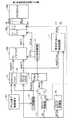
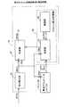
図1に示す第1実施形態は、内蔵されたリフレッシュ動作と外部アクセス動作とを互いに随時のタイミングで独立して動作させる動作仕様に、間引きリフレッシュ機能を付加した半導体記憶装置を示す。リフレッシュ動作と外部アクセス動作とを互いに独立して動作させることができるため、リフレッシュ動作のための外部コントローラが不要となり、擬似SRAMあるいは擬似SSRAMのSRAMあるいはSSRAMへの互換性をより完全なものとした上で、間引きリフレッシュ機能を備えることにより、スタンバイ時の消費電流の低減をも図った半導体記憶装置である。尚、図1では、ロウアドレス系に関する部分のみを示す。
【0058】
所定の制御端子101はI/O制御部13に接続され、制御端子101から入力される制御信号に応じて外部アクセス要求信号REQ(O)を出力する。外部アクセス要求信号REQ(O)は、所定ビット数のアドレス端子101から入力されるアドレス信号と共に、ロウアドレスバッファ11に接続され、ロウアドレスAdd(O)をロウプリデコーダ102に出力する。
【0059】
また、内蔵されているリフレッシュタイミング計時部14から所定時間ごとに出力されるリフレッシュトリガ信号RFTGは、リフレッシュアドレスカウンタ12とリフレッシュ制御部15に入力され、リフレッシュ制御部15からはリフレッシュ要求信号REQ(I)が出力される(後述の制御方法(2)の場合)。また、後述の制御方法(1)の場合には、リフレッシュトリガ信号RFTGがリフレッシュ要求信号REQ(I)として働く。リフレッシュアドレスカウンタ12からは、リフレッシュアドレスAdd(C)がロウプリデコーダ102に入力されると共に、リフレッシュアドレスAdd(C)のうちの所定の上位ビットが上位リフレッシュアドレスAdd(C)(m)として間引きリフレッシュ制御回路1に入力される。
【0060】
I/O制御部13から出力される外部アクセス要求信号REQ(O)と、リフレッシュトリガ信号RFTG(後述の制御方法(1)の場合)またはリフレッシュ要求信号REQ(I)(制御方法(2)の場合)とがアクセスアービタ16に入力される。アクセスアービタ16は、レベル信号またはパルス信号として入力される要求信号のレベル遷移を検出することにより、要求信号間の信号の先後を検出することができる。パルス信号が必要とされる場合には、リフレッシュトリガ信号RFTGの信号遷移をエッジとしてパルス信号を生成する回路を備えることで対応することができる(制御方法(1)の場合)。この場合、リフレッシュ制御部15はパルス信号を出力する構成とする。アクセスアービタ16からの出力信号は、ロウ系制御部17に入力され、ロウプリデコーダ102、メインロウデコーダ103、およびワードドライバ18に制御信号CTL1、CTL2を出力する。ここで、メインロウデコーダ103は、ロウプリデコーダ102から出力されるプリデコード信号AD(1)が入力され、メモリセルアレイ140に配置されているワード線WL0乃至WLnのうちワードドライバ18で駆動すべきワード線を選択する。
【0061】
間引きリフレッシュ制御回路1には、上位リフレッシュアドレスAdd(C)(m)のほか、リフレッシュトリガ信号RFTGが入力される。出力信号であるリフレッシュ実行許可信号RFENは、ワードドライバ18に入力されるか(制御方法(1))、リフレッシュ制御部15に入力される(制御方法(2))。
【0062】
第1実施形態の半導体記憶装置では、制御端子101からの制御信号の入力により要求される外部アクセス動作と、内蔵のリフレッシュタイミング計時部14から所定時間ごとに要求されるリフレッシュ動作とは、互いに独立に動作が要求される。そこで、アクセスアービタ16により、要求信号REQ(O)、REQ(I)間の調整を行なった上で、実行すべき動作を決定する。具体的には、制御端子101から入力される制御信号は、I/O制御部13に入力されて、外部アクセス要求信号REQ(O)としてアクセスアービタ16に外部アクセスの要求が出力される。リフレッシュタイミング計時部14から出力されるリフレッシュトリガ信号RFTGは、制御方法(1)の場合には直接、制御方法(2)の場合にはリフレッシュ制御部15を介して、リフレッシュ要求信号REQ(I)としてアクセスアービタ16にリフレッシュ動作の要求が出力される。
【0063】
アクセスアービタ16では、外部アクセス要求信号REQ(O)とリフレッシュ要求信号REQ(I)との何れか一方の要求信号が出力される場合には、要求されている動作を実行すべくロウ系制御部17が制御される。動作要求が競合する場合には、外部アクセス要求信号REQ(O)とリフレッシュ要求信号REQ(I)との調整が行なわれ、ロウ系制御部17が制御されて、外部アクセス動作とリフレッシュ動作とが引き続いて連続して行なわれる。
【0064】
ロウ系制御部17は、アクセスアービタ16による調整結果に応じて制御信号CTL1を出力し、ロウプリデコーダ102に入力すべきアドレス信号(Add(O)またはAdd(C))を選択する。また、制御信号CTL2を出力し、ロウプリデコーダ102でプリデコードされたプリデコード信号AD(1)をメインロウデコーダ103で更にデコードし、適当なタイミングでワードドライバ18を活性化して、デコードされて選択されたワード線(WL0乃至WLnのうちの何れかのワード線)を活性化する。すなわち、ロウ系制御部17は、アクセスアービタ16からの起動信号に基づき、適宜なタイミング差を有する一連の制御信号CTL1、CTL2を順次出力する。
【0065】
外部アクセス要求信号REQ(O)とリフレッシュ要求信号REQ(I)とが同時に入力される場合等には、アクセスアービタ16では、動作シーケンスの先後を決定する必要がある。データの消失回避を優先してリフレッシュ動作を先行させる制御、または外部アクセスの応答を優先して外部アクセス動作を先行させる制御の何れの制御を先行して選択することもできる。動作シーケンスの順序に関わらず、連続する両動作でサイクルタイムtCEが規定される。
【0066】
次に、間引きリフレッシュ機能について説明する。リフレッシュ動作ごとに、リフレッシュ動作の実行可否を間引きリフレッシュ制御回路1により判定してリフレッシュ実行許可信号RFENを出力する。第1実施形態では、リフレッシュ実行許可信号RFENにより間引きリフレッシュ動作を制御する2つの方法を示している(図1中、(1)および(2))。
【0067】
先ず、制御方法(1)について説明する。制御方法(1)では、リフレッシュタイミング計時部14によりリフレッシュトリガ信号RFTGが出力されると、リフレッシュアドレスカウンタ12がカウントアップされ、新たなリフレッシュアドレスAdd(C)が出力される。そして、このうちの所定の上位ビットについては、上位リフレッシュアドレスAdd(C)(m)として間引きリフレッシュ制御回路1に入力されて、新たに設定されたリフレッシュアドレスAdd(C)に対するリフレッシュ動作の実行可否の判定が行なわれる。
【0068】
ここで、間引きリフレッシュ制御回路1に入力されるのは、所定上位ビットの上位リフレッシュアドレスAdd(C)(m)としたが、例えば、最下位ビット以外のリフレッシュアドレスAdd(C)を入力すれば、判定の単位は2本のワード線を1単位として行なわれることとなり、下位2ビット以外のリフレッシュアドレスAdd(C)を入力すれば、判定の単位は4本のワード線を1単位として行なわれることとなる。上位ビットの設定に応じて判定の単位を自由に設定することができる。また、下位ビットを除外せず、リフレッシュアドレスAdd(C)の全ビットを入力して、ワード線ごとに判定を行なう構成とすることも可能である。
【0069】
判定結果であるリフレッシュ実行許可信号RFENは、ワードドライバ18に入力され、ワードドライバ18の活性化制御が行なわれる。リフレッシュ実行許可信号RFENによりリフレッシュ動作の実行が許可される場合には、ワードドライバ18は活性化される。リフレッシュ動作の実行が禁止される場合には、ワードドライバ18は非活性化状態に維持される。
【0070】
一方、リフレッシュタイミング計時部14から出力されるリフレッシュトリガ信号RFTGは、リフレッシュ要求信号REQ(C)としてアクセスアービタ16にも入力される。間引きリフレッシュ制御回路1における判定処理に並行して、外部アクセス要求信号REQ(O)との間でアクセス動作の調整が行なわれた上で、アドレス信号(Add(O)またはAdd(C))をデコードしてワード線を選択するロウ系の制御が行なわれる。すなわち、アクセスアービタ16によりリフレッシュ動作に調整されると、ロウ系制御部17が起動され制御信号CTL1が出力されて、ロウプリデコーダ102はリフレッシュアドレスAdd(C)をプリデコードすると共に、所定制御タイミングの後に出力される制御信号CTL2に応じて、メインロウデコーダ103により、プリデコード信号AD(1)がデコードされてリフレッシュ動作の対称であるワード線が選択される。
【0071】
間引きリフレッシュ制御回路1によるリフレッシュ動作の実行可否の判定は、リフレッシュ動作の対象となっている上位リフレッシュアドレスAdd(C)(m)が、リフレッシュ動作の実行可否が決定される記憶セルのデータ保持特性に基づき、予め格納されている所定アドレスに該当するか否かで判定される。すなわち、基本的にアドレスの一致比較で判定が行なわれる。これに対して、ワード線が駆動されるまでの処理は、アクセスアービタ16による要求信号REQ(O)、REQ(I)間の先着判断の処理、プリ/メインデコーダ102、103による多段の論理ゲートを介するデコード処理、更にはワードドライバ18によるワード線の駆動のための昇圧処理等、多数の処理をシーケンシャルに行なう必要がある。
【0072】
従って、一般的に、リフレッシュトリガ信号RFTGからリフレッシュ実行許可信号RFENに至るまでの判定時間に比して、リフレッシュトリガ信号RFTGからメインロウデコーダ103によるワード線の選択までの処理時間のほうが長くなる。そのため、間引きリフレッシュ制御回路1によるリフレッシュ動作の実行可否の判定処理を、ロウ系の処理時間の中に完全に埋め込ませることができる。
【0073】
間引きリフレッシュ制御回路1によりリフレッシュ動作の実行が許可される場合には、ワードドライバ18が活性化状態に設定された後にメインロウデコーダ103によりデコードされてワード線が選択されるため、ロウ系の処理時間を増大させることなくリフレッシュ動作が行なわれる。リフレッシュ動作の実行が禁止される場合には、ワードドライバ18の非活性化状態への設定に遅れてメインロウデコーダ103でのデコードが行なわれるため、デコードにより選択されるワード線が駆動されることはなくリフレッシュ動作は行なわれない。
【0074】
尚、第1実施形態では、リフレッシュ実行許可信号RFENをワードドライバ18の活性化制御に使用する場合について説明したが、アクセスアービタ16により起動される制御信号CTL1、CTL2の制御タイミングに応じて、ロウプリデコーダ102からワードドライバ18までで行なわれるリフレッシュアドレスAdd(C)のデコード処理の処理時間との関係で、間引きリフレッシュ制御回路1の判定処理時間が間に合えば、リフレッシュ実行許可信号RFENによる活性化制御を、ワードドライバ18に代えて、メインロウデコーダ103等の前段回路に対して行なうことも可能である。
【0075】
次に、制御方法(2)について説明する。制御方法(1)と同様に、リフレッシュトリガ信号RFTGによるリフレッシュアドレスカウンタ12のカウントアップで生成される、新たなリフレッシュアドレスAdd(C)のうち所定の上位ビットが、上位リフレッシュアドレスAdd(C)(m)として間引きリフレッシュ制御回路1に入力されて、リフレッシュ動作の実行可否の判定が行なわれる。
【0076】
制御方法(2)では、リフレッシュトリガ信号RFTGをリフレッシュ要求信号REQ(I)としてアクセスアービタ16に出力するリフレッシュ制御部15を備えており、判定結果であるリフレッシュ実行許可信号RFENはリフレッシュ制御部15に入力されリフレッシュ制御部15が活性化制御されて、リフレッシュ要求信号REQ(I)の出力制御を行なう。リフレッシュ実行許可信号RFENによりリフレッシュ動作の実行が許可される場合には、リフレッシュ要求信号REQ(I)がアクセスアービタ16に出力される。リフレッシュ動作の実行が禁止される場合には、リフレッシュ要求信号REQ(I)は出力されない。
【0077】
すなわち、リフレッシュトリガ信号RFTGに対して、設定されたリフレッシュアドレスAdd(C)におけるリフレッシュ動作の実行可否の判定結果に応じて、リフレッシュ要求信号REQ(I)がアクセスアービタ16に出力されることとなる。これに対して、外部アクセス要求信号REQ(O)は、制御端子101から入力される制御信号に応じてI/O制御部13から随時出力される。従って、外部アクセス動作とリフレッシュ動作の競合状態においては、外部アクセス要求信号REQ(O)に対して、リフレッシュ要求信号REQ(I)がリフレッシュ動作の実行可否の判定時間分の遅延を伴って出力されることとなる。
【0078】
すなわち、アクセスの競合状態において、リフレッシュトリガ信号RFTGに引き続いて外部アクセスの要求が発生した場合、または設定によっては同時にアクセスが発生した場合、本来なら、リフレッシュ動作が先行し引き続いて外部アクセス動作が行なわれるところ、判定時間分の遅延によりリフレッシュ要求信号REQ(I)が外部アクセス要求信号REQ(O)に遅延してアクセスアービタ16に入力される可能性がある。この場合は、動作シーケンスは逆転してしまうものの、間引きリフレッシュ制御回路1における判定処理を、先行する外部アクセス動作に完全に埋め込ませることができるため、外部アクセス動作とリフレッシュ動作との連続動作で規定されるサイクルタイムが本来の規定に対して長くなってしまうことはない。
【0079】
また、リフレッシュ動作において、間引きリフレッシュ制御によりリフレッシュ動作が禁止される場合には、要求信号に対する調整処理から、アドレスのデコード処理、さらにワード線の駆動処理に至るまでの一連のロウ系の処理動作が禁止される。不要な消費電流の低減をすることができる。
【0080】
尚、所定上位ビットの上位リフレッシュアドレスAdd(C)(m)のビット数の設定については、制御方法(1)の場合と同様であり、同様の作用・効果を奏するので、ここでの説明は省略する。
【0081】
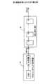
図2は、上位リフレッシュアドレスAdd(C)(m)の間引きリフレッシュ制御回路1への入力例を示す。間引きリフレッシュ制御回路1の入力段には、専用アドレスデコーダ1Aが備えられており、入力される上位リフレッシュアドレスAdd(C)(m)に応じてデコードされた専用デコード信号AD(2)が、間引きリフレッシュの判定を行なう間引きリフレッシュ制御部19に入力されている。
【0082】
専用デコード信号AD(2)は、上位リフレッシュアドレスAdd(C)(m)をデコードしたデコード信号であるため、専用アドレスデコーダ1Aに入力する上位リフレッシュアドレスAdd(C)(m)に応じて、除外された下位アドレスのビット数分、間引きリフレッシュ制御部19におけるリフレッシュ動作の実行可否の判定単位を広くすることができる。除外すべき下位アドレスのビット数を適宜に設定してやれば、好適な判定単位でリフレッシュ動作の実行可否の判定を行なうことができる。所定ワード線ごとに間引きリフレッシュの有無を設定するためのアドレスを格納するヒューズ等によるダイサイズの増大を抑えながら、ワード線の所定単位毎に間引きリフレッシュの実行可否の判定を行なって消費電流の低減を図ることができる。
【0083】
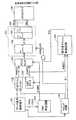
図3には、専用アドレスデコーダ1Aを備えて好適な場合のレイアウト例を示す。図3では、リフレッシュアドレスカウンタ12を、アドレス端子101ごとに配置されるロウアドレスバッファ11の近傍に分散配置する場合である。また、リフレッシュアドレスカウンタ12と間引きリフレッシュ制御部19とは、離間して配置されているとする。
【0084】
このようなレイアウトにおいて、間引きリフレッシュ制御部19に入力されるアドレス信号を、ロウプリデコーダ102から出力されるプリデコード信号AD(1)とすることも考えられる。しかしながら、間引きリフレッシュ制御部19までの配線経路が長いため、配線の寄生容量等に起因してプリデコード信号AD(1)に付随する容量負荷CLDは多大となる。プリデコード信号AD(1)は、ワード線の選択が行なわれるためにメインロウデコーダ103にも入力されているため、多大な容量負荷CLDによるプリデコード信号AD(1)の駆動遅延の結果、ワード線の選択までのロウ系の処理時間が遅延してしまうおそれがある。
【0085】
そこで、専用アドレスデコーダ1Aを備えることにより、間引きリフレッシュ制御部19へのアドレス信号の伝播を、専用デコード信号AD(2)に受け持たせる構成としている。メインロウデコーダ103に入力されるプリデコード信号AD(1)から不要な容量負荷CLDが排除され、プリデコード信号AD(1)の駆動遅延を必要最小限とすることができる。
【0086】
図4に示す第2実施形態は、第1実施形態と同様に、内蔵されたリフレッシュ動作と外部アクセス動作とを互いに随時のタイミングで独立して動作させる動作仕様に、間引きリフレッシュ機能を付加した場合であり、擬似SRAM等のSRAM等への互換性をより完全なものとした上で、間引きリフレッシュ機能を備えることにより、スタンバイ時の消費電流の低減をも図った半導体記憶装置である。
【0087】
第2実施形態では、リフレッシュアドレスAdd(C)が入力される間引きリフレッシュ制御回路1に代えて、ロウプリデコーダ102から出力されるプリデコード信号AD(1)が入力される間引きリフレッシュ制御回路2が備えられている。
【0088】
プリデコード信号AD(1)からワード線が駆動されるまでの、メインデコーダ103による多段の論理ゲートを介するデコード処理、およびワードドライバ18によるワード線駆動のための昇圧処理等のシーケンシャルな処理に対して、一般的に、アドレスの一致比較による判定処理は短時間で行なわれる。従って、第1実施形態の制御方法(1)の場合と同様に、間引きリフレッシュ制御回路2によるリフレッシュ動作の実行可否の判定処理を、ロウ系の処理時間の中に完全に埋め込ませることができる。
【0089】
また、ロウプリデコーダ102から出力されるプリデコード信号AD(1)を供給する構成としたため専用アドレスデコーダは不要となり、半導体記憶装置におけるダイサイズの増大を抑制することができる構成である。その他の構成については、第1実施形態の制御方法(1)の場合と同様であり、同様の作用、効果を奏するので、ここでの説明は省略する。
【0090】
図5は、プリデコード信号AD(1)の間引きリフレッシュ制御回路2への入力例を示す。間引きリフレッシュ制御回路2の入力段にはバッファ部2Aが備えられており、入力されるプリデコード信号AD(1)を、制御信号SELCに応じて取り込むことができる。バッファ部2Aは、例えば、アンド論理ゲートで構成することができる。この他にも、制御信号SELCでプリデコード信号AD(1)の入力を制御できる構成であれば適用できることは言うまでもない。制御信号SELCで制御されるトランスファゲート等で構成することもできる。
【0091】
図6は、図3における専用アドレスデコーダ1Aに代えて、バッファ部2Aを備えて好適な場合のレイアウト例を示す。この場合、バッファ部2Aは、ロウプリデコーダ102の近傍に配置されているものとする。尚、リフレッシュアドレスカウンタ12がアドレス端子101ごとに配置されるロウアドレスバッファ11の近傍に分散配置されている点、およびリフレッシュアドレスカウンタ12と間引きリフレッシュ制御部19とが離間して配置されて点は図3の場合と同様である。
【0092】
このようなレイアウトでは、ロウプリデコーダ102から間引きリフレッシュ制御部19までの長い配線経路に寄生する多大な容量負荷CLDは、ロウプリデコーダ102の近傍に配置されているバッファ部2Aにより分断される。このため、ロウプリデコーダ102からメインロウデコーダ103へのプリデコード信号AD(1)の経路に不要な容量負荷CLDが付加されることはなく、プリデコード信号AD(1)の駆動遅延を必要最小限とすることができる。
【0093】
次に、図7乃至図11に、第1および第2実施形態におけるアクセス動作波形を例示する。図7は、擬似SRAMにおいて、リフレッシュ要求と外部アクセス要求とが競合する場合である。図7では、外部アクセス要求に対してリフレッシュ要求が先行する場合(図7中、左側の動作波形)と、両アクセス要求が同時に発生する場合(図7中、右側の動作波形)を示す。ここで、アクセス要求が同時の場合には、リフレッシュ動作を先行させる設定の場合を示す。
【0094】
通常の場合、リフレッシュ動作の実行可否の判定は、リフレッシュ動作内において行なわれる。具体的には、図24において、CBR判定回路133から出力されるリフレッシュ指示信号φCBRにより生成されるリフレッシュアドレスAdd(C)が、間引きリフレッシュ制御回路105により判定されて、判定結果がリフレッシュ許可信号φ2として出力されることにより、アンド論理ゲート400bがゲーティングされて活性化信号φRが出力される。この活性化信号φRがロウアドレスデコーダ137を活性化する信号であり、第1および第2実施形態においてロウ系制御部17から最初に出力される制御信号CTL1に該当する信号である。すなわち、図24、図25の場合では、間引きリフレッシュ制御回路105による判定処理の後、ロウアドレスのデコードが開始されることとなり、リフレッシュ動作の実行時間に判定時間が加算されることとなる。
【0095】
図7における通常の場合の動作波形では、この判定時間tJが、リフレッシュ動作の実行時間とは別に加算されることを示す。このため、リフレッシュ動作と外部アクセス動作との実行時間に加えて、間引きリフレッシュの実行可否を判定するための判定時間tJが加算されて、アクセス競合の場合におけるサイクルタイムtCE'が規定されることとなる。リフレッシュ動作と外部アクセス動作との連続した実行時間が間引き制御を行なわない場合のアクセス競合におけるサイクルタイムtCEであるから、この時間に判定時間tJが加算されてサイクルタイムtCE'(=tCE+tJ)が規定されることとなり、サイクルタイムの増大を招くこととなる。
【0096】
これに対して、第1および第2実施形態では、判定時間tJがリフレッシュ動作の実行時間または外部アクセス動作の実行時間に埋め込まれる。第1実施形態のうちの制御方法(1)および第2実施形態の場合では、リフレッシュトリガ信号RFTGがリフレッシュ要求信号としてアクセスアービタ16に入力される場合である。リフレッシュトリガ信号RFTGにより出力されるリフレッシュアドレスAdd(C)に基づき、間引き判定がされると共にリフレッシュ動作が開始される。判定時間tJは、リフレッシュ動作の実行時間における前半部分に埋め込まれるので、判定処理が本来のリフレッシュ動作を律速することはなく、リフレッシュ動作と外部アクセス動作との連続した実行時間でサイクルタイムtCEが規定される。
【0097】
第1実施形態のうちの制御方法(2)の場合では、リフレッシュトリガ信号RFTGにより出力されるリフレッシュアドレスAdd(C)に基づき、間引き判定が先行して行なわれる。この期間は、リフレッシュ制御部15は非活性状態を維持しているため、アクセスアービタ16にリフレッシュ要求信号REQ(I)が出力されることはない。この判定処理の期間に外部アクセス要求信号REQ(O)が発生すれば、外部アクセス動作が先行して行なわれることとなる。判定処理は、外部アクセス動作の実行時間における前半部分に埋め込まれるので、判定処理が本来のリフレッシュ動作を律速することはなく、外部アクセス動作を律速することもないので、リフレッシュ動作と外部アクセス動作との連続した実行時間でサイクルタイムtCEが規定される。尚、この場合の競合動作は、先行するリフレッシュトリガ信号の発生時点から遅れて外部アクセス要求信号REQ(O)の発生時点から開始されるが、外部アクセス動作が本来のアクセスより遅延することはない。
【0098】
図8乃至図11は、擬似SSRAM等の同期型の半導体記憶装置において、バースト動作中にリフレッシュ動作を埋め込ませる場合について示す。図8、9はバースト長1の場合であり、図10、11は多バースト長の場合である。
【0099】
ここで、リフレッシュ動作を埋め込ませるとは、バーストサイクル中にリフレッシュ動作を埋め込ませることにより、バースト動作を中断することなくリフレッシュ動作をも行なえる動作仕様のことを示す。
【0100】
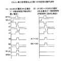
図8に示す通常の場合におけるバースト長1の動作では、CASレイテンシ3でオートプリチャージ動作を伴うリード動作(RDAコマンドで動作)を行なう場合である。図7において説明したとおり、間引きリフレッシュ機能について、リフレッシュ動作の実行可否の判定を独立して行なわなければならない場合が存在する。すなわち、バースト動作が終了してビット線のイコライズ動作が行なわれているクロックCLK9においてリフレッシュ要求信号REQ(I)が発生する場合である。間引きリフレッシュ機能がなければクロックCLK9のサイクルでイコライズ動作を終了した後(図8中、信号EQのハイレベル期間)、クロックCLK10のサイクルでリフレッシュ動作用のワード線WLが立ち上がるところ、間引きリフレッシュ機能によりクロックCLK9においてリフレッシュ要求信号REQ(I)が発生するため、リフレッシュ動作の実行可否の判定を行なった上で、リフレッシュ動作が許可される場合には次サイクルのクロックCLK10のサイクルでリフレッシュアドレスAdd(C)のデコード処理が行なわれる。すなわち、間引きリフレッシュ機能を導入することに伴い、1サイクル分の判定時間が必要となり、専用のクロックサイクルを1サイクル追加しなければならなくなる(図8中、クロックCLK10)。間引きリフレッシュ機能がない場合のRASサイクルタイムtRASが15クロックサイクルであるのに比して、1クロックサイクル追加した16クロックサイクルが必要となってしまう。
【0101】
これに対して、図9の動作波形は、第1実施形態における制御方法(1)および第2実施形態の場合を示しており、図7で説明したように、判定処理がリフレッシュ動作のアドレスデコード時間に埋め込まれる。判定処理とリフレッシュアドレスAdd(C)のデコード処理とが同一のクロックサイクル(図9中、クロックCLK9)で並列処理されるため、間引きリフレッシュ機能を導入しても、専用のクロックサイクルは追加する必要はなく、間引きリフレッシュ機能がない場合のRASサイクルタイムtRASと同じ15クロックサイクルで、間引きリフレッシュ機能を有するリフレッシュ動作を埋め込ませることができる。
【0102】
図10には、通常の場合における多バースト長の動作として、バースト長16の動作波形を示す。図8のバースト長1の動作波形と同様に、CASレイテンシ3でオートプリチャージ動作を伴うリード動作(RDAコマンドで動作)を行なう場合である。図10に示すリフレッシュ動作を埋め込ませる多バースト長の動作では、ビット線対(BLと/BL)からデータを読み出す際のスイッチの開閉は、クロックCLKには同期せず、これより速い周期で動作させる。即ち、クロックCLKによる読み出しのタイミングに先行してデータが読み出されることとなる。先行して読み出されたデータは、データバッファ回路等の一時保持回路(不図示)に保持されており、その後の読み出しタイミングであるクロックCLKに同期して外部に出力する仕様である。先行してデータを読み出すため、ビット線対(BLと/BL)を外部仕様に比して速いタイミングでイコライズすることができる。このため、クロックCLK13でイコライズ動作に移行することができる。
【0103】
しかしながら、この場合もバースト長1の動作と同様に(図8、参照)、間引きリフレッシュ機能について、リフレッシュ動作の実行可否の判定を独立して行なわなければならない場合が存在する。すなわち、ビット線のイコライズ動作が行なわれているクロックCLK13においてリフレッシュ要求信号REQ(I)が発生すると、間引きリフレッシュ機能がなければリフレッシュ動作用のワード線WLが立ち上がるクロックCLK14で、リフレッシュアドレスAdd(C)のデコード処理を行なわなければならない。すなわち、間引きリフレッシュ機能を導入することに伴い、専用のクロックサイクルを1サイクル追加しなければならなくなり(図10中、クロックCLK14)、間引きリフレッシュ機能がない場合のRASサイクルタイムtRASが20クロックサイクルであるのに比して、1クロックサイクル追加した21クロックサイクルが必要となってしまう。
【0104】
これに対して、図11の動作波形は、第1実施形態における制御方法(1)および第2実施形態の場合を示しており、図9の場合と同様に、判定処理がリフレッシュ動作のアドレスデコード時間に埋め込まれる。判定処理とリフレッシュアドレスAdd(C)のデコード処理とが同一のクロックサイクル(図11中、クロックCLK13)で並列処理されるため、間引きリフレッシュ機能を導入しても、専用のクロックサイクルは追加する必要はなく、間引きリフレッシュ機能がない場合のRASサイクルタイムtRASと同じ20クロックサイクルで、間引きリフレッシュ機能を有するリフレッシュ動作を埋め込ませることができる。
【0105】
尚、図9、11では、第1実施形態のうちの制御方法(1)および第2実施形態の場合を想定して動作を説明したが、第1実施形態のうちの制御方法(2)の場合においても、判定処理を埋め込ませることができることは、擬似SRAMのアクセス競合の場合について図7で説明した場合と同様であるので、ここでの説明は省略する。
【0106】
以上詳細に説明したとおり、第1実施形態の制御方法(1)および第2実施形態によれば、間引きリフレッシュ制御回路1、2でのリフレッシュ動作の実行可否の判定処理を、対応アドレスであるリフレッシュアドレスAdd(C)のデコード処理時間の中に埋め込ませることができる。そのため、リフレッシュ動作の実行可否の判定時間tJがリフレッシュ動作を含んだ外部アクセス動作との競合アクセス時の実行時間であるサイクルタイムtCEに付加されて、サイクルタイムtCEが増大することはない。また、バースト動作中にリフレッシュ動作を埋め込ませる動作仕様の場合にも、判定時間tJがRASサイクルタイムtRASに付加されてクロックサイクルを増加させることはなく、RASサイクルタイムtRASが増大することはない。
【0107】
また、第1実施形態の制御方法(2)によれば、間引きリフレッシュ制御回路1でのリフレッシュ動作の実行可否の判定前の段階では、リフレッシュ要求信号REQ(I)はアクセスアービタ16に入力されず調整用信号とならないので、実行可否の判定処理中に外部アクセス要求信号REQ(O)が生成されれば、直ちに外部アクセス動作が行なわれる。実行可否の判定時間tJが、外部アクセス動作の遅延として付加されることはない。従って、判定時間tJが、リフレッシュ動作を含んだ外部アクセス動作との競合アクセス時の実行時間であるサイクルタイムtCEに付加されて、サイクルタイムtCEが増大することはない。また、バースト動作中にリフレッシュ動作を埋め込ませる動作仕様の場合にも、判定時間tJがRASサイクルタイムtRASに付加されて、クロックサイクルを増加させることはなく、RASサイクルタイムtRASが増大することはない。
【0108】
また、リフレッシュ要求信号REQ(I)に対してリフレッシュ動作を禁止する判定がされる場合には、リフレッシュ要求信号REQ(I)が外部アクセス要求信号REQ(O)との間で調整に供されることはない。すなわち、リフレッシュ動作の禁止判定の場合には、要求信号間の調整部であるアクセスアービタ16以降の、対応アドレスであるリフレッシュアドレスAdd(C)のデコード処理が動作することはなく、不要な回路動作を止めて消費電流の低減を図ることができる。
【0109】
また、第1実施形態における専用アドレスデコーダ1Aによれば、間引きリフレッシュ制御部19において、対応アドレス群であるデコードされた専用デコード信号AD(2)ごとに、ヒューズ、ROM、RAM等で構成される格納部を備えればよく、リフレッシュ動作の対象となるワード線についてのアドレスごとに備える場合に比して、半導体記憶装置のダイサイズにおける格納部の占有面積を縮小することができる。
【0110】
また、リフレッシュ動作の実行可否の判定に必要となる専用デコード信号AD(2)の指定を、専用のデコーダである専用アドレスデコーダ1Aを備えて、リフレッシュ動作の対象とされる対応アドレスである上位リフレッシュアドレスAdd(C)(m)のデコードにより行なうので、リフレッシュ動作の実行可否の判定に際して、ロウプリデコーダ102の負荷が増大することはない。リフレッシュ動作の可否判定が不要な設定の場合、または外部アクセス動作の場合にも、ロウプリデコーダ102の負荷が増大することはない。リフレッシュ動作の実行可否の判定機能を導入しても、アクセス動作の負担の増大を招くことはなく、消費電流の増大やサイクルタイムの遅延等が招来されることはない。
【0111】
また、専用デコード信号AD(2)を、専用アドレスデコーダ1Aにより独立に指定できるので、ロウプリデコーダ102のデコード処理に制約されることなく、判定の単位としてまとめられるリフレッシュ要求信号REQ(I)の発生回数を設定して、専用デコード信号AD(2)を指定することができる。リフレッシュ動作の実行可否の判定単位は専用デコード信号AD(2)ごとにまとめられるので、リフレッシュ動作の実行の必要がないワード線を含んでリフレッシュ動作の実行の判定がなされる場合があるが、上位リフレッシュアドレスAdd(C)(m)の選択により、専用デコード信号AD(2)でまとめられるリフレッシュ要求信号REQ(I)の発生回数を調整して、間引きリフレッシュによる消費電流の低減を、格納部による占有面積の増大を抑制しながら実現することができる。
【0112】
また、第2実施形態によれば、実行可否の判定を行なう対応アドレス群であるプリデコード信号AD(1)の指定を、ロウプリデコーダ102で共用することができ、リフレッシュ動作の実行可否判定の機能を導入しても半導体記憶装置のダイサイズの増大を抑制することができる。
【0113】
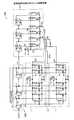
図12に、第3実施形態として、間引きリフレッシュ制御回路の回路ブロック図を示す。リフレッシュトリガ信号RFTGは、間引きリフレッシュ制御部19内の切り替え部31に入力される。切り替え部31からは、リフレッシュトリガ信号RFTGに応じて間引きリフレッシュ制御の活性・非活性を切り替える切り替え制御信号SELCが出力される。切り替え制御信号SELCは、比較部33および判定部34に入力され、これらの回路の活性化制御を行なっている。また、専用アドレスデコーダ1Aまたはバッファ部2Aにも入力され、同様に活性化制御を行っている。
【0114】
比較部33には、専用アドレスデコーダ1Aまたはバッファ部2Aより、リフレッシュ動作の実行可否の判定対象である、プリデコード信号AD(1)または専用デコード信号AD(2)が入力され、格納部32に格納されている所定のデータ保持特性を有する記憶セルが接続されているワード線を含んだ所定アドレスAD(TO)との間でアドレスの一致比較が行なわれる。ここで、所定アドレスAD(TO)は、プリデコード信号AD(1)または専用デコード信号AD(2)と同一レベルのデコード信号であることはいうまでもない。格納部32と比較部33とによりリフレッシュ実力記憶部30を構成している。
【0115】
比較部33による比較結果は判定部34に出力され、切り替え制御信号SELCの設定状態に応じて、リフレッシュ実行許可信号RFENが出力される。
【0116】
以上に説明したように、第3実施形態として例示した間引きリフレッシュ制御回路では、間引きリフレッシュ動作をさせない場合に、切り替え部31から出力される切り替え制御信号SELCにより、専用アドレスデコーダ1Aまたはバッファ部2A、比較部33、および判定部34が非活性化されるので、不要な回路動作による消費電流を低減することができる。
【0117】
図13には、第3実施形態における切り替え部31の具体例を示す。リフレッシュタイミング計時部14は、オシレータ回路と分周器とで構成されており、オシレータ回路からの発振信号が分周されて、リフレッシュトリガ信号RFTGが出力される。切り替え部31は、所定数のフリップフロップでカウンタが構成されている。リフレッシュトリガ信号RFTGの発生回数を計数することにより、リフレッシュ周期tREFを計時している。
【0118】
リフレッシュトリガ信号RFTGごとにワード線を順次選択してリフレッシュ要求が行なわれるので、リフレッシュすべきワード線数のリフレッシュトリガ信号RFTGの出力を計数すれば、リフレッシュ周期tREFを計時することができる。リフレッシュ周期tREFの2周期ごとに間引きリフレッシュ制御を行なう設定であれば、リフレッシュ周期tREFの計時ごとに切り替え制御信号SELCを切り替えて、間引きリフレッシュ制御回路の活性・非活性を切り替えることができる。
【0119】
リフレッシュトリガ信号RFTGの出力回数を計数することにより、リフレッシュ周期tREFを計時することができるので、リフレッシュアドレスAdd(C)が一回りすることによりリフレッシュ周期tREFを計時する方法においては必要であった、リフレッシュアドレスAdd(C)の初期化あるいは初期値の記憶等の処理が不要となる。初期化あるいは初期値の記憶等の処理回路が不要となり、制御回路の簡易化および低消費電流化を図ることができる。
【0120】
図14には、第3実施形態における専用アドレスデコーダ1Aの具体例を示す。図14の具体例では、リフレッシュ動作の実行可否の判定単位として、リフレッシュアドレスAdd(C)のうち上位の4ビットを選択して、上位リフレッシュアドレスAdd(C)(N−3)〜(N)としている。ここで、Nは最上位ビットを表している。各上位リフレッシュアドレスAdd(C)(N−3)〜(N)は、切り替え制御信号SELCとともにナンド論理ゲートに入力されている。各ナンド論理ゲートの出力からは正/逆の相補信号が生成されて、アドレスごとの全ての組み合わせに対して論理積出力が出力されることによりデコードが行なわれる。デコード信号AD0〜AD3は、リフレッシュアドレスAdd(C)(N−3)および(N−2)について、(0、0)、(0、1)、(1、0)、(1、1)の組み合わせに対する信号であり、デコード信号BD0〜BD3は、リフレッシュアドレスAdd(C)(N−1)および(N)について、(0、0)、(0、1)、(1、0)、(1、1)の組み合わせに対する信号である。尚、デコード処理は、切り替え制御信号SELCがハイ論理レベルのとき活性化され、ロー論理レベルのときはアドレス値にかかわらず一定の出力に固定されてデコード処理は非活性となる。
【0121】
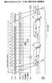
図15は、第3実施形態におけるリフレッシュ実力記憶部30の具体例である。切り替え制御信号SELCとリフレッシュトリガ信号RFTGとが入力されるナンド論理ゲートの出力端子n1は、直列に接続された2段のインバータ論理ゲートの入力端子に接続されるとともに、第2段のインバータ論理ゲートの出力端子n3とあわせ、ナンド論理ゲートの入力端子に接続され、出力端子n4がPMOSトランジスタのゲート端子に接続されている。このPMOSトランジスタの一方の端子は電源電圧に接続されている。専用アドレスデコーダ1Aでデコードされたデコード信号AD0〜AD3、BD0〜BD3は、初段のインバータゲートの出力端子n2とともに、各々、ナンド論理ゲートに入力された後、インバータ論理ゲートで反転されパルスデコード信号A0〜A3、B0〜B3が出力される。
【0122】
パルスデコード信号A0〜A3とB0〜B3とは、各々組み合わされて、16通りの組み合わせで直列接続された2段のNMOSトランジスタのゲート端子に入力される。16組の2段構成のNMOSトランジスタ列の一方の端子は接地電圧に接続され、他方はヒューズ素子F0〜F15を介して端子n5でPMOSトランジスタのドレイン端子に接続される。端子n5はインバータ論理ゲートの入力端子に接続されて、インバータ論理ゲートの出力端子からリフレッシュ判定信号RFFGが出力される。
【0123】
図15では、データ保持特性が良好で、リフレッシュ動作を間引くことが可能な記憶セルが接続されているワード線を含むパルスデコード信号に対して、ヒューズ(F0〜F15)を切断する構成である。未切断のヒューズ(図15の場合、ヒューズ0(F0))に対応するパルスデコード信号(A0、B0)で指定されるワード線には、データ保持特性が悪くリフレッシュ周期tREFごとにリフレッシュ動作を実行しなければならない記憶セルを含む。
【0124】
図16は、第3実施形態における判定部34を構成する第1の判定部の具体例である。リフレッシュ判定信号RFJG、またはリフレッシュトリガ信号RFTGが入力されるナンド論理ゲートが各々備えられており、他方の入力端子には、切り替え制御信号SELC、およびその反転信号が各々入力されている。2組のナンド論理ゲートの出力端子は、ナンド論理ゲートの入力端子に接続されており、その出力端子からリフレッシュ実行許可信号RFENが出力されている。
【0125】
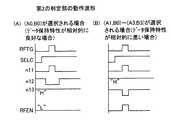
図17に、リフレッシュ実力記憶部(図15)と、第1の判定部(図16)との動作を示す動作波形である。図17中、(A)はパルスデコード信号(A0、B0)が選択された場合を、(B)はパルスデコード信号(A1、B0)〜(A3、B3)が選択された場合を示す。
【0126】
先ず、(A)、(B)の各々に共通な動作について説明する。切り替え制御信号SELCがハイ論理レベルとなり、間引きリフレッシュ制御が活性化されている状態で、リフレッシュトリガ信号RFTGにハイ論理レベルのパルス信号が入力され、リフレッシュ要求が発せられると、端子n1には論理反転されたロー論理レベルのパルス信号が出力され、更に、反転・遅延して端子n2にハイ論理レベルのパルス信号が出力される。同様に、端子n3には遅延したロー論理レベルのパルス信号が出力される。端子n1、n3のロー論理レベルのパルス信号により、端子n4には端子n1のパルスから端子n3のパルスまで拡張されたハイ論理レベルのパルス信号が出力され、この間、PMOSトランジスタをオフして端子n5の電源電圧への充電を停止する。
【0127】
(A)では、端子n2のパルス信号に基づき、パルスデコード信号A0およびB0がハイ論理レベルのパルス信号を出力する。これにより、パルスデコード信号A0、B0が入力されているNMOSトランジスタ列は導通し、端子n5との間に接続されているヒューズ0(F0)が切断されていないため、端子n5は接地電圧に放電されてロー論理レベルとなる。その後、端子n4がロー論理レベルに遷移するため、PMOSトランジスタが再び導通して、端子n5をハイ論理レベルに充電する。この結果、端子n5には、ロー論理レベルのパルス信号が出力され、インバータ論理ゲートで反転されて、リフレッシュ実行許可信号RFENとしてハイ論理レベルのパルス信号が出力される。
【0128】
(B)では、端子n2のパルス信号に基づき、パルスデコード信号(A1、B0)〜(A3、B3)の何れかの組み合わせがハイ論理レベルのパルス信号を出力する。これにより、パルスデコード信号(A1、B0)〜(A3、B3)の何れかの組み合わせが入力されているNMOSトランジスタ列は導通する。しかし、(B)の場合では、端子n5との間に接続されているヒューズ(F1〜F15)が何れも切断されているため、端子n5から接地電圧に至る経路は確立されず、端子n5の電圧は電源電圧に維持される。この結果、インバータ論理ゲートで反転されて、リフレッシュ実行許可信号RFENはロー論理レベルに維持される。
【0129】
図14、15に示した具体例では、最上位ビットからの上位4ビットでリフレッシュアドレスAdd(C)(m)が設定されている場合を示したが、選択される上位ビット数はこれに限定されるものではない。リフレッシュ実力記憶部30に備えるべきヒューズの配置占有面積と、間引きリフレッシュ制御が複数のワード線ごとにまとめられることによる間引きリフレッシュ機能による消費電流の低減効果とは、トレードオフの関係にある。両者の調整を図り適宜な設定とすることができる。
【0130】
図18は、第3実施形態における判定部34を構成する第2の判定部の具体例である。第1の判定部(図16)が、データ保持特性が良好でリフレッシュ動作を間引くことができるワード線を含む場合にヒューズを切断する処理を行なうのに対して、データ保持特性が相対的に悪くリフレッシュ動作を間引くことができないワード線を含む場合にヒューズを切断する処理を行なう場合の設定である。
【0131】
ここで、記憶セルのデータ保持特性の実力に応じて、リフレッシュ周期tREFが決定される。すなわち、データ保持特性が相対的に悪い記憶セルに対しては、より短い周期でリフレッシュを行なうことが必要である。リフレッシュ周期tREFは、データ保持特性が悪い記憶セルに律速して設定されるため、データ保持特性が相対的に良好な記憶セルに対しては、リフレッシュ要求信号に応じてリフレッシュ動作の実行可否を判定して必要に応じてリフレッシュ動作を実行してやればよいが、データ保持特性が相対的に悪い記憶セルに対しては、リフレッシュ要求信号ごとにリフレッシュ動作を実行する必要がある。
【0132】
第2の判定部では、第1の判定部(図16)における切り替え制御信号SELCとリフレッシュ判定信号RFJGとが入力されるナンド論理ゲートに代えて、3入力のナンド論理ゲートを備える。3入力のナンド論理ゲートには、切り替え制御信号SELC、端子n11に出力されるリフレッシュトリガ信号RFTGを所定遅延時間τだけ遅延させた遅延信号、および端子n12に出力されるリフレッシュ判定信号RFJGのハイ論理レベルのパルス信号を所定時間拡張したロー論理レベルのパルス信号が入力される。
【0133】
図19に動作波形を示す。図19中、(A)はパルスデコード信号(A0、B0)が選択された場合を、(B)はパルスデコード信号(A1、B0)〜(A3、B3)が選択された場合を示す。
【0134】
(A)、(B)に共通な動作として、切り替え制御信号SELCがハイ論理レベルの状態で、リフレッシュトリガ信号RFTGにハイ論理レベルのパルス信号が入力されると、所定遅延時間τの後に端子n11にハイ論理レベルの遅延したパルス信号が出力される。
【0135】
(A)では、リフレッシュ実力記憶部30(図15)でヒューズ0(F0)が未切断なので、リフレッシュ判定信号RFJGとしてハイ論理レベルのパルス信号が出力される。第2の判定部において、このパルス信号が論理反転された上でパルス幅が拡張されて、ロー論理レベルのパルス信号として端子n12に出力される。このとき、端子n11に出力されるハイ論理レベルのパルス信号が端子n12のパルス信号の期間に埋め込まれるように、所定遅延時間τが設定されている。これにより、3入力のナンド論理ゲートの何れかの入力端子は、ロー論理レベルの信号が入力されていることとなり、出力端子n13はハイ論理レベルを維持する。ここで、他方のナンド論理ゲートの出力もハイ論理レベルに維持されているので、リフレッシュ実行許可信号RFENはロー論理レベルに維持される。
【0136】
(B)では、リフレッシュ実力記憶部30(図15)でヒューズ(F1〜F15)が切断されており、リフレッシュ判定信号RFJGはロー論理レベルに維持される。従って、第2の判定部において、端子n2はハイ論理レベルに維持される。これにより、端子n11のハイ論理レベルのパルス信号に基づき、3入力のナンド論理ゲートの出力端子n13にはロー論理レベルのパルス信号が出力され、ハイ論理レベルのパルス信号としてリフレッシュ実行許可信号RFENが出力される。
【0137】
以上に説明したように第3実施形態の具体例によれば、第2の判定部を有効にする場合には、第1の判定部を有効にする場合に対して、ヒューズの切断論理やリフレッシュ判定信号RFJGの意味が逆転して設定されることとなる。従って、第1および第2の判定部を切り替えて使用する設定にすることが有効である。初期段階で第1の判定部を有効にしておき、データ保持特性が良好な記憶セルを含む場合にヒューズを切断する論理とする。製造上の要因によりデータ保持特性が良好な記憶セルが増え、リフレッシュ実力記憶部30に備えられているヒューズ群で対応できなくなった場合に、第2の判定部に切り替える。これにより、データ保持特性が悪い記憶セルについてヒューズ切断を行なう論理に反転されるので、ヒューズ切断数を削減することができる。リフレッシュ実力記憶部30に備えるべきヒューズ数を限定することができ、ヒューズ群の占有目積を抑制することができる。
【0138】
第1の判定部と第2の判定部との切り替えは、切り替え用のヒューズを1本備えることで対応することができる。例えば、各々の判定部から出力されるリフレッシュ実行許可信号RFENを、トランスファゲートを介して供給するように設定しておく。何れか一方のトランスファゲートのみを導通させるので、各トランスファゲートへの制御信号は相補の関係にある。切り替え用ヒューズにより論理関係を逆転させることで判定部の切り替えを行なうことができる。
【0139】
半導体記憶装置内の記憶セルが有するデータ保持特性の分布に応じて、リフレッシュ実力記憶部30内の格納部32に格納すべき所定アドレスを切り替え、リフレッシュ動作の実行可否の判定を切り替えることができるので、データ保持特性の分布に合わせて、格納部32に格納すべき所定アドレスが少なくなるように切り替えることができる。格納部32に備えるべきヒューズ等の配置数を圧縮して半導体記憶装置のダイサイズの増大を抑制することができる。
【0140】
また、格納すべき所定アドレス数が圧縮されるため、格納部32への所定アドレスの格納処理の手続きを軽減することができる。処理時間の短縮、それに伴う処理費用の削減をすることができる。
【0141】
尚、第1/第2の判定部の設定について、初期段階において第1の判定部を有効にしておく場合について説明したが、第2の判定部を有効にしておくこともできる。更に、第1/第2の判定部の切り替えをヒューズにより行なうとして説明したが、ヒューズ以外にも、RAM、ROM,レジスタ等の状態を記憶しておく記憶手段を用いることができることは言うまでもない。
【0142】
また、データ保持特性の分布に応じて切り替える場合、出荷検査等の試験において測定された特性分布に応じて切り替えることのほか、使用温度や使用電源電圧等の使用環境に応じて変化する特性に合わせて、切り替えることも可能である。この場合、事情対設定の記憶手段を、ヒューズに代えて、書き換え可能なRAM等にしておけば、環境の変化に応じて切り替え設定を可変とすることもできる。
【0143】
図20に、第4実施形態として、試験容易化機能を備えた間引きリフレッシュ制御回路4を示す。間引きリフレッシュ制御部19の入力部には、プリデコード信号AD(1)あるいは専用デコード信号AD(2)、または試験アドレス入力用の外部端子44からの試験用のアドレス信号を入力するために、試験信号TESTにより切り替えられるスイッチ部41を備える。また、間引きリフレッシュ制御部19の出力部には、試験信号TESTにより、リフレッシュ実行許可信号RFENを、試験結果出力用の外部端子45に出力するための、アンド論理ゲート42と、試験結果出力部43とを備える。
【0144】
通常の動作状態では、例えば、試験信号TESTをロー論理レベルにする。スイッチ部41は、プリデコード信号AD(1)または専用デコード信号AD(2)に接続され、リフレッシュ動作の実行可否を判定すべきアドレス信号が入力される。また、アンド論理ゲート42の出力はロー論理レベルに固定されるため、試験結果出力部43を非活性状態に維持することができる。従って、この場合、試験アドレス入力用の外部端子44および試験結果出力用の外部端子45は、試験以外の端子として使用することができる。
【0145】
試験状態では、例えば、試験信号TESTをハイ論理レベルにする。スイッチ部41は、試験アドレス入力用の外部端子44に接続され、外部から設定されるアドレス信号が入力される。また、アンド論理ゲート42の出力にはリフレッシュ実行許可信号RFENと同相の信号が出力されるため、試験結果出力部43を介して試験結果出力用の外部端子45に試験結果を出力することができる。この場合、試験用のアドレスを外部端子44から自由に入力することができ、内蔵のリフレッシュアドレスカウンタ等の制御を待つことなく、迅速、的確に必要なアドレスを供給して試験を行なうことができる。不良解析や特性解析に適用して有効な試験容易化機能を提供することができる。
【0146】
以上に説明したように第4実施形態によれば、必要に応じて、間引きリフレッシュ制御部19におけるリフレッシュ動作の実行可否の判定結果を外部から観測することができるので、半導体記憶装置の不良解析や特性調査等に利用することができ、特性試験を効率的に実施することができる。
【0147】
図21乃至図23に、第5実施形態として、冗長領域における間引きリフレッシュ制御について説明する。
図21は第1具体例である。間引きリフレッシュ制御用のアドレスを格納するヒューズ切断の際に、冗長設定のデータを利用して冗長領域を示すヒューズも切断する処理についてのフローチャートである。
【0148】
先ず、データ収集処理段階について説明する。ステップ(以下、Sと略記する)10において、冗長データを取得する。動作特性が不良である不良記憶セルに関するアドレスデータを取得し、これらのアドレス領域の記憶セルについては、冗長領域を使用するためである。取得したデータは、冗長アドレスデータ(D1)として記憶される。更に、記憶セルにおけるデータ保持特性を取得する(S20)。データ保持特性の良否に応じて、リフレッシュ動作における間引き制御を行なう領域を決定するためのデータの取得である。取得したデータのうちデータ保持特性が相対的に悪く間引きリフレッシュの対象とすることができないアドレスについて、非間引きアドレスデータ(D2)として記憶される。次に、データ保持特性の分布に応じて、間引きリフレッシュ用のヒューズ切断論理を確定する(S30)。データ保持特性の良好な記憶セルが多数である場合には、ヒューズ切断をデータ保持特性の悪いアドレスに設定し、逆に、データ保持特性の良好な記憶セルが少数である場合には、ヒューズ切断をデータ保持特性の良好なアドレスに設定するための処理である。論理の確定結果は、間引きリフレッシュ用ヒューズ切断論理データ(D3)として記憶される。
【0149】
次に、ヒューズ切断処理段階の説明である。間引きリフレッシュ用ヒューズ切断論理データ(D3)に基づき、非間引きアドレスについてヒューズ切断を行なう場合には(S50:YES)、冗長アドレスデータ(D1)と非間引きアドレスデータ(D2)とを加算したデータを切断用データとしてロードする(S60)。非間引きアドレスについてヒューズ切断を行なわない場合には(S50:NO)、全アドレスから、冗長アドレスデータ(D1)と非間引きアドレスデータ(D2)とを除外したアドレスを切断用データとしてロードする(S70)。そして、ロードしたデータに基づき、間引きリフレッシュ制御用のヒューズ切断を行なう。
【0150】
以上に説明した、第5実施形態の第1具体例によれば、S60では、データ保持特性が悪く間引きリフレッシュ制御を行なわない非間引きアドレスと冗長アドレスとを加算してヒューズ切断を行ない、S70では、全アドレスから、冗長アドレスと非間引きアドレスとを除外してヒューズ切断を行なう。従って、冗長領域については、間引き制御を行なわない設定とすることができる。
【0151】
冗長設定されている冗長記憶セルについてはリフレッシュ動作の実行可否の判定がされないため、この冗長記憶セルについてデータ保持特性を測定し、必要に応じて、冗長アドレスのうちの間引きリフレッシュ制御を行なう所定アドレスを選別するという試験が不要となる。試験時間の増大を抑制することができる。
【0152】
また、冗長領域については、冗長設定を行なったデータをそのまま利用して、間引きリフレッシュ用のヒューズを切断することができるので、冗長領域に対して間引きリフレッシュ制御を実施しないための制御回路等が不要である。
【0153】
図22は、第2具体例である。リフレッシュアドレスAdd(C)に対して、冗長設定がされているか否かを判断した上で、間引きリフレッシュ制御回路を制御する構成を示した回路ブロック図である。
【0154】
リフレッシュアドレスAdd(C)が生成されると、冗長判定部51において冗長領域140iに冗長設定されているか否かが判定される。冗長設定されていると判定されれば、冗長信号REDiが出力され、該当する冗長領域140iに対してアクセスが行なわれる。冗長領域140iは、半導体記憶装置の構成に応じて複数のブロックに分割されていることが一般的であるので、冗長信号REDiも、分割された冗長領域140iごとに生成される。
【0155】
これらの冗長信号REDiは、オア論理ゲート52により論理和された上で、冗長設定信号REDとして、間引きリフレッシュ制御回路5の非活性化端子INHに入力される。間引きリフレッシュ制御回路5では、冗長設定信号REDが入力されると非活性化状態となり、間引き制御を禁止することができる。これにより、冗長領域においては間引き制御を行なわない設定とすることができる。
【0156】
以上に説明した、第5実施形態の第2具体例によれば、冗長領域における間引き制御の禁止を、冗長判定部51から出力され、冗長領域140iをアクセスする冗長信号REDiにより行なうことができる。従って、特性試験において、冗長設定のデータを利用して間引きリフレッシュ制御回路に対して特別の処理を行なう必要がなく、試験時間を短縮することができる。
【0157】
図23は、コラム冗長を示すレイアウト概念図である。コラム冗長の構成を、ロウアドレス方向にブロック分割した単位で行なう。このような設定とすれば、コラム冗長された所定ブロック単位ごとに間引きリフレッシュ制御を禁止することができる。コラム冗長領域におけるデータ保持特性の測定等の煩雑な処理を回避してコラム冗長領域については間引きリフレッシュ制御を行なわない設定としながら、その領域をブロック分割された領域に限定することができるので、コラム冗長設定されていない領域については間引きリフレッシュ制御による消費電流の低減を図ることができ、コラム冗長において、冗長設定における煩雑な処理の回避と間引きリフレッシュによる消費電流の低減とを両立させることができる。
【0158】
尚、本発明は前記実施形態に限定されるものではなく、本発明の趣旨を逸脱しない範囲内で種々の改良、変形が可能であることは言うまでもない。
例えば、本実施形態においては、第1乃至第5実施形態について、個別に説明したが、これらの構成または方法は、適宜に組み合わせることができることは言うまでもない。
【0159】
(付記1) リフレッシュ要求信号に応じて、対象となるワード線を順次選択してリフレッシュ動作を行なう半導体記憶装置において、
複数の前記リフレッシュ要求信号において前記リフレッシュ動作の対象とされるワード線群についての対応アドレス群を指定する指定部と、
所定のデータ保持特性を有する記憶セルが接続されているワード線を含む所定ワード線群についての所定アドレス群を予め格納する格納部と、
前記指定部により指定される前記対応アドレス群と、前記格納部に格納されている前記所定アドレス群とを比較する比較部と、
前記比較部による比較結果に応じて、前記リフレッシュ動作の実行可否が判定される判定部とを備えることを特徴とする半導体記憶装置。
(付記2) 前記指定部は、前記リフレッシュ動作の対象とされる前記ワード線についての対応アドレスをデコードするロウアドレスデコーダとは別の専用デコーダを備えることを特徴とする付記1に記載の半導体記憶装置。
(付記3) 前記指定部は、前記リフレッシュ動作の対象とされる前記ワード線についての対応アドレスをデコードするロウアドレスデコーダを含むことを特徴とする付記1に記載の半導体記憶装置。
(付記4) リフレッシュ要求信号に応じて、対象となるワード線を順次選択してリフレッシュ動作を行なう半導体記憶装置において、
前記リフレッシュ要求信号に応じて前記リフレッシュ動作の対象となるワード線についての対応アドレスを指定する指定部、および、前記対応アドレスと、所定のデータ保持特性を有する記憶セルが接続されている所定ワード線についての所定アドレスとを比較し、比較結果に応じて前記リフレッシュ動作の実行可否が判定される判定部を備える間引きリフレッシュ制御部と、
前記間引きリフレッシュ制御部の活性状態を所定条件において切り替える切り替え部とを備え、
前記間引きリフレッシュ制御部を機能させない場合には、前記切り替え部により前記指定部または前記判定部の少なくとも一方を非活性化することを特徴とする半導体記憶装置。
(付記5) 前記切り替え部は、所定時間を計時する計時部を備え、
前記所定時間ごとに前記間引きリフレッシュ制御部の活性状態を切り替えることを特徴とする付記4に記載の半導体記憶装置。
(付記6) 前記計時部は、前記リフレッシュ要求信号の発生回数を計数する計数部を備えることを特徴とする付記5に記載の半導体記憶装置。
(付記7) リフレッシュ要求信号に応じて、対象となるワード線を順次選択してリフレッシュ動作を行なう半導体記憶装置において、
前記リフレッシュ動作の対象となるワード線についての対応アドレスと比較される所定アドレスを格納する格納部と、
記憶セルが有するデータ保持特性の分布に応じて、前記格納部に格納すべき前記所定アドレスを、第1のデータ保持特性を有する記憶セルを含むアドレスと、第2のデータ保持特性を有する記憶セルを含むアドレスとの間で切り替える格納切り替え部と、
前記格納切り替え部による切り替えに応じて、比較による前記リフレッシュ動作の実行可否の判定結果を切り替える判定部とを備えることを特徴とする半導体記憶装置。
(付記8) 前記第1のデータ保持特性とは、所定のデータ保持特性以上または所定のデータ保持特性より良好なデータ保持特性であり、前記第2のデータ保持特性とは、所定のデータ保持特性より劣悪または所定のデータ保持特性以下のデータ保持特性であり、
前記判定部は、前記第1または第2のデータ保持特性を有する記憶セルを含む前記所定アドレス間で、前記リフレッシュ動作の実行可否の判定結果を反転することを特徴とする付記7に記載の半導体記憶装置。
(付記9) リフレッシュ要求信号に応じて、対象となるワード線を順次選択してリフレッシュ動作を行なう半導体記憶装置において、
前記対象となるワード線についての対応アドレスと、所定のデータ保持特性を有する記憶セルが接続されている所定ワード線についての所定アドレスとを比較し、比較結果に応じて前記リフレッシュ動作の実行可否が判定される間引きリフレッシュ制御部と、
試験時に活性化され、前記間引きリフレッシュ制御部からの判定結果を外部に出力する出力部とを備えることを特徴とする半導体記憶装置。
(付記10) 前記試験時に、前記判定結果を前記出力部に伝播するバッファ部を備えることを特徴とする付記9に記載の半導体記憶装置。
(付記11) 前記試験時に、前記間引きリフレッシュ制御部に入力されるアドレスを、前記対応アドレスに代えて外部から入力される試験アドレスに切り替えるアドレス切り替え部を備えることを特徴とする付記9に記載の半導体記憶装置。
(付記12) リフレッシュ要求信号に応じて、対象となるワード線を順次選択してリフレッシュ動作を行なう半導体記憶装置において、
前記対象となるワード線についての対応アドレスと、所定のデータ保持特性を有する記憶セルが接続されている所定ワード線についての所定アドレスとを比較し、比較結果に応じて前記リフレッシュ動作の実行可否が判定される間引きリフレッシュ制御部と、
不良記憶セルを救済するための冗長記憶セルとを備え、
前記対応アドレスのうち前記冗長記憶セルへの冗長設定が行なわれている冗長アドレスについては、前記間引きリフレッシュ制御部による判定は行なわれないことを特徴とする半導体記憶装置。
(付記13) 前記冗長設定は、前記冗長記憶セルを含む所定数のワード線を冗長領域の基本単位として行なわれ、該冗長領域の基本単位については、前記間引きリフレッシュ制御部による判定は行なわれないことを特徴とする付記12に記載の半導体記憶装置。
(付記14) 前記冗長領域は、コラム冗長であることを特徴とする付記13に記載の半導体記憶装置。
(付記15) 前記間引きリフレッシュ制御部は、所定のデータ保持特性を有する記憶セルが接続されている所定ワード線についての所定アドレスを予め格納する格納部を備え、
前記格納部は、更に、前記冗長アドレスが格納されることを特徴とする付記12に記載の半導体記憶装置。
(付記16) 前記対応アドレスが前記冗長アドレスであるか否かの判定を行なう冗長判定部を備え、また、
前記間引きリフレッシュ制御部は、前記対応アドレスに対して前記リフレッシュ動作の実行可否が判定される判定部を備え、
前記冗長判定部による冗長判定に基づき、前記判定部が制御されることを特徴とする付記12に記載の半導体記憶装置。
(付記17) 外部アクセス要求信号に基づき行なわれる外部アクセス動作と、内部で自動的に生成されるリフレッシュ要求信号に基づき行なわれるリフレッシュ動作とが互いに独立して実行される半導体記憶装置において、
前記外部アクセス要求信号と前記リフレッシュ要求信号との調整を図る調整部と、
前記調整部により決定される前記外部アクセス動作または前記リフレッシュ動作の何れかの動作に対して、対応アドレスのデコード処理を制御する制御部と、
前記制御部により起動される、前記対応アドレスのロウアドレスデコーダ、および前記ロウアドレスデコーダにより選択されるワード線を駆動するワード線駆動部と、
前記リフレッシュ要求信号に応じて出力される前記対応アドレスに対して前記リフレッシュ動作の実行可否が判定される間引きリフレッシュ制御部とを備え、
前記ロウアドレスデコーダまたは前記ワード線駆動部は、前記間引きリフレッシュ制御部による判定結果に基づき活性化制御されることを特徴とする半導体記憶装置。
(付記18) 外部アクセス要求信号に基づき行なわれる外部アクセス動作と、内部で自動的に生成されるリフレッシュ要求信号に基づき行なわれるリフレッシュ動作とが互いに独立して実行される半導体記憶装置において、
前記外部アクセス要求信号と前記リフレッシュ要求信号との調整を図る調整部と、
前記リフレッシュ要求信号を前記調整部に出力するリフレッシュ要求部と、
前記リフレッシュ要求信号に応じて出力される対応アドレスに対して前記リフレッシュ動作の実行可否が判定される間引きリフレッシュ制御部とを備え、
前記間引きリフレッシュ制御部による判定結果に基づき、前記リフレッシュ要求部が制御されることを特徴とする半導体記憶装置。
(付記19) リフレッシュ要求信号に応じて、対象となるワード線を順次選択してリフレッシュ動作を行なう半導体記憶装置のリフレッシュ制御方法において、
複数の前記リフレッシュ要求信号において前記リフレッシュ動作の対象とされるワード線群についての対応アドレス群ごとに、該ワード線群に接続されている記憶セルにおけるデータ保持特性に応じて、前記リフレッシュ動作の実行可否が判定されることを特徴とする半導体記憶装置のリフレッシュ制御方法。
(付記20) 前記対応アドレス群は、前記リフレッシュ動作に応じて対象とされる前記ワード線についての対応アドレスをデコードして得られる対応デコードアドレスにより指定され、
前記対応デコードアドレスと、所定のデータ保持特性を有する記憶セルが接続されているワード線を含んで予め格納されている所定デコードアドレスとが比較されることにより、前記リフレッシュ動作の実行可否が判定されることを特徴とする付記19に記載の半導体記憶装置のリフレッシュ制御方法。
(付記21) リフレッシュ要求信号に応じて、対象となるワード線を順次選択してリフレッシュ動作を行なう半導体記憶装置のリフレッシュ制御方法において、
前記対象となるワード線についての対応アドレスのうち冗長設定が行なわれている冗長アドレスについては、前記リフレッシュ動作の実行可否の判定は行なわれないことを特徴とする半導体記憶装置のリフレッシュ制御方法。
(付記22) 前記冗長設定は、前記冗長記憶セルが記憶されている所定数のワード線を冗長領域の基本単位として行なわれ、該冗長領域の基本単位については、前記間引きリフレッシュ制御部による判定は行なわれないことを特徴とする付記21に記載の半導体記憶装置のリフレッシュ制御方法。
(付記23) 前記冗長設定は、コラム冗長であることを特徴とする付記22に記載の半導体記憶装置のリフレッシュ制御方法。
(付記24) 前記冗長アドレスは、所定のデータ保持特性を有する記憶セルが接続されている所定ワード線についての所定アドレスと共に、予め格納されていることを特徴とする付記21に記載の半導体記憶装置のリフレッシュ制御方法。
(付記25) 外部アクセス要求信号に基づき行なわれる外部アクセス動作と、内部で自動的に生成されるリフレッシュ要求信号に基づき行なわれるリフレッシュ動作とが互いに独立して実行される半導体記憶装置のリフレッシュ制御方法において、
前記外部アクセス要求信号と前記リフレッシュ要求信号との調整により前記リフレッシュ動作が選択され、前記リフレッシュ動作の対象である対応アドレスのデコード処理と引き続き行なわれるワード線の駆動処理とに並行して、前記対応アドレスに対する前記リフレッシュ動作の実行可否の判定処理が行われ、
前記実行可否の判定結果に基づき、前記デコード処理または前記ワード線の駆動処理の活性化制御が行なわれることを特徴とする半導体記憶装置のリフレッシュ制御方法。
(付記26) 外部アクセス要求信号に基づき行なわれる外部アクセス動作と、内部で自動的に生成されるリフレッシュ要求信号に基づき行なわれるリフレッシュ動作とが互いに独立して実行される半導体記憶装置のリフレッシュ制御方法において、
前記外部アクセス要求信号と前記リフレッシュ要求信号との調整を図るアクセス動作調整工程と、
前記アクセス動作調整工程により決定される前記外部アクセス動作または前記リフレッシュ動作の何れかの動作に対して、対応アドレスのデコード処理を制御する制御工程と、
前記制御工程により起動される、前記対応アドレスのデコードを行なうロウアドレスデコード工程、および引き続き行なわれるワード線駆駆動工程とを有し、
前記アクセス動作調整工程から前記ワード線駆動工程に至る処理と並行して、前記対応アドレスに対する前記リフレッシュ動作の実行可否が判定される間引きリフレッシュ制御工程を有し、
前記間引きリフレッシュ制御工程による判定結果に基づき、前記ロウアドレスデコード工程または前記ワード線駆動工程の活性化制御が行なわれることを特徴とする半導体記憶装置のリフレッシュ制御方法。
(付記27) 外部アクセス要求信号に基づき行なわれる外部アクセス動作と、内部で自動的に生成されるリフレッシュ要求信号に基づき行なわれるリフレッシュ動作とが互いに独立して実行される半導体記憶装置のリフレッシュ制御方法において、
前記リフレッシュ要求信号に応じて出力される対応アドレスに対して前記リフレッシュ動作の実行可否が判定され、
該判定結果に基づき、前記リフレッシュ要求信号が、前記外部アクセス要求信号との間で調整されることを特徴とする半導体記憶装置のリフレッシュ制御方法。
(付記28) 外部アクセス要求信号に基づき行なわれる外部アクセス動作と、内部で自動的に生成されるリフレッシュ要求信号に基づき行なわれるリフレッシュ動作とが互いに独立して実行される半導体記憶装置のリフレッシュ制御方法において、
前記リフレッシュ要求信号に応じて出力される対応アドレスに対して、前記リフレッシュ動作の実行可否が判定される間引きリフレッシュ制御工程と、
前記間引きリフレッシュ制御工程による判定結果に基づき、前記リフレッシュ要求信号が有効とされるリフレッシュ要求工程と、
有効とされた前記外部アクセス要求信号と前記リフレッシュ要求信号との調整を図るアクセス動作調整工程とを有することを特徴とする半導体記憶装置のリフレッシュ制御方法。
(付記29) 冗長設定を行ないながら、リフレッシュ要求信号ごとにリフレッシュ動作の実行可否判定に応じてリフレッシュ動作を行なう半導体記憶装置についての試験方法であって、
前記冗長設定を行なうべき冗長アドレスを取得する冗長アドレス取得工程と、
所定のデータ保持特性を有する記憶セルについての所定アドレスを取得する所定アドレス取得工程と、
前記冗長アドレスと前記所定アドレスとを、前記実行可否判定の対象から除外するために、前記半導体記憶装置内に予め格納しておく格納工程とを有することを特徴とする半導体記憶装置についての試験方法。
【0160】
【発明の効果】
本発明によれば、従来の半導体記憶装置では不十分であった消費電流の更なる低減を図ることが可能となり、更に、互換性を高めた擬似SRAM等に適用しても動作上の遅延増大を招くことのない、好適な間引きリフレッシュ機能を実現することにより、スタンバイ状態での消費電流の低減を図ることが可能な半導体記憶装置を提供することが可能となる。
【図面の簡単な説明】
【図1】 第1実施形態の半導体記憶装置の回路ブロック図である。
【図2】 第1実施形態の間引きリフレッシュ制御回路へのアドレス入力例を示す回路ブロック図である。
【図3】 専用アドレスデコーダを備えて好適なレイアウト配置例を示すレイアウト図である。
【図4】 第2実施形態の半導体記憶装置の回路ブロック図である。
【図5】 第2実施形態の間引きリフレッシュ制御回路へのアドレス入力例を示す回路ブロック図である。
【図6】 ロウプリデコーダからのプリデコード信号を受けるバッファ部を備えて好適なレイアウト配置例を示すレイアウト図である。
【図7】 擬似SRAMにおけるアクセス競合を示す動作波形図である。
【図8】 擬似SSRAMにおけるバースト長1の動作波形図である(通常動作)。
【図9】 擬似SSRAMにおけるバースト長1の動作波形図である(第1および第2実施形態の場合)。
【図10】 擬似SSRAMにおける多バースト長の動作波形図である(通常動作)。
【図11】 擬似SSRAMにおける多バースト長の動作波形図である(第1および第2実施形態の場合)。
【図12】 間引きリフレッシュ制御回路を示す回路ブロック図である(第3実施形態)。
【図13】 第3実施形態における切り替え部を示す回路ブロック図である。
【図14】 第3実施形態における専用アドレスデコーダを示す回路ブロック図である。
【図15】 第3実施形態におけるリフレッシュ実力記憶部を示す回路ブロック図である。
【図16】 第3実施形態における第1の判定部を示す回路ブロック図である。
【図17】 リフレッシュ実力記憶部および第1の判定部の動作を示す動作波形図である。
【図18】 第3実施形態における第2の判定部を示す回路ブロック図である。
【図19】 第2の判定部の動作を示す動作波形図である。
【図20】 試験容易化機能を備えた間引きリフレッシュ制御回路を示す回路ブロック図である(第4実施形態)。
【図21】 冗長領域における間引きリフレッシュ制御(第5実施形態)の第1具体例を示すフロー図である。
【図22】 冗長領域における間引きリフレッシュ制御(第5実施形態)の第2具体例を示す回路ブロック図である。
【図23】 ロウアドレス方向にブロック分割されたコラム冗長構成を示すレイアウト概念図である。
【図24】 従来技術の半導体記憶装置の回路ブロック図である。
【図25】 従来技術の間引きリフレッシュ制御回路を中心に示す回路ブロック図である。
【符号の説明】
1 間引きリフレッシュ制御回路
1A 専用アドレスデコーダ
2 間引きリフレッシュ制御回路
2A バッファ部
11 ロウアドレスバッファ
12 リフレッシュアドレスカウンタ
13 I/O制御部
14 リフレッシュタイミング計時部
15 リフレッシュ制御部
16 アクセスアービタ
17 ロウ系制御部
18 ワードドライバ
19 間引きリフレッシュ制御部
30 リフレッシュ実力記憶部
31 切り替え部
32 格納部
33 比較部
34 判定部
41 スイッチ部
43 試験結果出力部
44 試験アドレス入力用の外部端子
45 試験結果出力用の外部端子
101 制御端子、アドレス端子
102 ロウプリデコーダ
103 メインロウデコーダ
140 メモリセルアレイ
Add(C) リフレッシュアドレス
Add(C)(m) 上位リフレッシュアドレス
AD(1) プリデコード信号
AD(2) 専用デコード信号
CTL1、CTL2 制御信号
REQ(O) 外部アクセス要求信号
REQ(I) リフレッシュ要求信号
RFEN リフレッシュ実行許可信号
RFTG リフレッシュトリガ信号
SELC 切り替え制御信号
TEST 試験信号[0001]
BACKGROUND OF THE INVENTION
The present invention relates to a semiconductor memory device, and more particularly to reduction of current consumption in a standby state.
[0002]
[Prior art]
In a semiconductor memory device that requires a refresh operation, the refresh operation must be performed periodically even during standby, which requires a low current consumption operation, and it is essential to reduce the current consumption in the refresh operation.
[0003]
In general, a memory cell mounted on a semiconductor memory device has a certain width in retention characteristics of stored data. For this reason, the refresh cycle tREF, which is the time interval at which the same memory cell is refreshed, must be set for the worst value of the data retention characteristics, but for memory cells with better data retention characteristics, It is sufficient to perform the refresh operation with a period longer than the refresh period tREF. Thus, a so-called thinning refresh operation is proposed in which a refresh operation is performed once every two or more refresh cycles tREF for a memory cell having good data retention characteristics. As a result, the number of refresh operations per predetermined time is reduced, and current consumption during the refresh operation can be reduced.
[0004]
Japanese Unexamined Patent Publication No. 9-102193 discloses a semiconductor memory device having a thinning refresh function. FIG. 24 mainly shows a circuit configuration of a row address system. A case where a thinning refresh function is provided in a / CAS before / RAS (hereinafter abbreviated as CBR) refresh operation is illustrated.
[0005]
The
[0006]
The
[0007]
[0008]
[0009]
[0010]
The refresh address Add (C) output from the
[0011]
The
[0012]
That is, in the normal write / read cycle, control signal / RAS falls before control signal / CAS, and output signal φCBR of
[0013]
In the CBR refresh cycle, control signal / CAS falls before control signal / RAS, so that output signal φCBR of
[0014]
FIG. 25 shows a circuit diagram centering on the thinning
[0015]
Each address registration circuit 1.1-1. r is an NMOS transistor 600, fuses 7.0 to 7.N provided corresponding to address signals A0 'to An' and their inverted signals / A0 'to / An'. n and NMOS transistors 8.0-8. n and fuses 7.0 'to 7. n ′ and NMOS transistors 8.0 ′ to 8. n ′.
[0016]
The refresh address Add (C) is supplied to the address registration circuits 1.1 to 1.. If the address matches one of the addresses registered in r, the address registration circuits 1.1-1. Any one of the outputs φH1 to φHr of r becomes high level, and the refresh permission signal φ2 becomes high level.
[0017]
In recent years, as functions required for devices have increased with the spread of portable devices, larger capacity memories are required instead of static random access memories (hereinafter referred to as SRAMs) that have been conventionally installed. Has reached. Since it is necessary to mount this in a limited space at a realistic price, a DRAM or the like is used while using a memory cell of a dynamic random access memory (hereinafter referred to as DRAM) having a high integration and a low cost per bit instead of an SRAM memory cell. A DRAM with a built-in refresh function, called a so-called pseudo SRAM, which has built-in control related to the refresh operation peculiar to the memory cell has been used. Thus, if the external controller outputs a self-refresh command or a control signal for performing a self-refresh operation during a period when there is no external access, the so-called self-refresh mode in which the pseudo SRAM itself performs control of the refresh address and the like is performed. It has been installed. Also, in response to future high-speed requests, a so-called pseudo-SSRAM specification that is compatible with the external specification of a synchronous SRAM (hereinafter referred to as SSRAM) is becoming realistic.
[0018]
[Problems to be solved by the invention]
However, in the semiconductor memory device having the thinning refresh function exemplified in JP-A-9-102193, the address registration circuits 1.1 to 1. r, it is necessary to register a row address that needs to be refreshed every refresh cycle tREF. For each row address, the address registration circuits 1.1 to 1.. r is required. Further, each address registration circuit 1.1-1. For r, a fuse corresponding to the bit width of the row address is required. In other words, the total number of fuses that must be mounted in the semiconductor memory device requires (row address bit width) × (number of row addresses to be refreshed every cycle). In order to obtain an effective reduction effect of current consumption by the refresh operation with respect to the distribution of data retention characteristics in the semiconductor memory device, a large number of fuses must be provided, which may increase the die size of the semiconductor memory device. It is a problem.
[0019]
Also, the address registration circuits 1.1-1. When an address is registered in r, a large amount of test time is required to cut a large number of fuses. In addition, the refresh address Add (C) is generated by the built-in counter, and there are restrictions on external control, and in the setting of thinning-out refresh control for redundant areas to replace defective cells, a functional test is performed. In some cases, a large amount of test time is required for implementation, which is a problem.
[0020]
Further, since the refresh address Add (C) is connected to the thinning
[0021]
Conventionally, in a semiconductor memory device referred to as a pseudo SRAM or a pseudo SSRAM, the load on the external controller for the refresh operation is greatly reduced, but control by the external controller is still necessary. In some cases, it is necessary to provide a dedicated control terminal for the control. Therefore, it cannot be said that a conventional pseudo SRAM or the like is completely compatible with an SRAM or an SSRAM that originally does not require such control or control terminal. Therefore, in order to bring this compatibility closer to perfection, the refresh operation and the normal data read / write operation as the external access operation are independent from each other at any time while the refresh operation is incorporated as the internal access operation. There has been proposed a semiconductor memory device having specifications that operate in the same manner. However, when the thinning refresh function is added to this semiconductor memory device, the refresh operation time is due to the refresh address determination time by the thinning refresh control circuit and the propagation delay due to the load on the signal path of the refresh address described above. May become long, and the cycle time in operation may be long, which is a problem.
[0022]
The present invention has been made to solve the above-described problems of the prior art, and further reduces the current consumption, which has been insufficient in the conventional semiconductor memory device, and provides a pseudo SRAM and the like with improved compatibility. The main object is to provide a semiconductor memory device capable of reducing current consumption in a standby state by realizing a suitable thinning refresh function that does not cause an increase in operational delay even when applied. And
[0023]
[Means for Solving the Problems]
In order to achieve the above object, a semiconductor memory device according to
[0024]
According to another aspect of the semiconductor memory device of the present invention, the thinning refresh control unit that performs thinning out of the refresh operation includes a storage unit, a comparison unit, and a determination unit, and is targeted by a plurality of refresh request signals designated by the designation unit. Address for the word line groupWithA storage cell having a first data retention characteristic stored in the storage unit and requiring a refresh operation in the refresh cycle, or a second data retention characteristic not requiring a refresh operation in the refresh cycle , A predetermined address for a predetermined word line group including a word line connected toWithAre compared in the comparison section, and depending on the comparison resultWhether the corresponding address specified by the specification unit is the target of thinning control in the refresh operationDetermined by the determination unitDo.
In addition, the storage switching unit determines a predetermined address to be stored in the storage unit in accordance with the distribution of the data retention characteristics of the memory cells in the semiconductor memory device, and the data retention characteristics of the first and second data retention characteristics. When the address including the memory cell having the first data retention characteristic is stored by the determination unit, the comparison result by the comparison unit is inconsistent. Further, when an address including a memory cell having the second data retention characteristic is stored, if the comparison result by the comparison unit is the same, it is determined that the corresponding address is a target of thinning control in the refresh operation. Do.
[0025]
As a result, the fuse, ROM, RAM, etc. provided for storing in the storage unit need only be provided for each corresponding address group, compared with the case where each fuse is provided for each address for the target word line according to the refresh request signal. Thus, the area occupied by the storage portion in the die size of the semiconductor memory device can be reduced.
In addition, the predetermined address to be stored in the storage unit can be switched according to the distribution of the data retention characteristics of the memory cells in the semiconductor memory device, and the determination result of whether or not the refresh operation can be performed can be switched. According to the distribution, switching can be performed so that the number of predetermined addresses to be stored in the storage unit is reduced. An increase in the die size of the semiconductor memory device can be suppressed by compressing the number of fuses, ROM, RAM, and the like to be provided in the storage unit.
Further, since the number of predetermined addresses to be stored is compressed, the procedure for storing the predetermined addresses in the storage unit can be reduced. It is possible to shorten the processing time and the processing cost associated therewith.
[0026]
Here, the determination unit for whether or not the refresh operation can be performed is the corresponding address.SugoTherefore, there is a case where the execution of the refresh operation is determined including a word line that does not need to be refreshed. Conversely, in the setting for determining whether or not each word line can be executed, it is necessary to provide a storage unit for each address of the word line, and the area occupied by the storage unit becomes large. In other words, the occupied area of the storage unit and the reduction of current consumption due to thinning refresh are in a contradictory relationship. Supported addressInBy adjusting the number of occurrences of the refresh request signals to be collected, it is possible to reduce current consumption by the thinning refresh operation while suppressing an increase in the occupied area by the storage unit.
Further, the refresh period tREF is determined according to the ability of the data retention characteristics of the memory cell. That is, it is necessary to perform a refresh operation in a shorter cycle for a memory cell having relatively poor data retention characteristics. Since the refresh cycle tREF is rate-determined and set for a memory cell with poor data retention characteristics, whether or not a refresh operation can be performed is determined according to the refresh request signal for a memory cell with relatively good data retention characteristics. Then, the refresh operation may be executed as necessary. On the other hand, for a memory cell having relatively poor data retention characteristics, it is necessary to execute a refresh operation for each refresh request signal.
[0027]
In the semiconductor memory device according to the second aspect, it is preferable that the corresponding address for the word line group to be refreshed is specified based on a part of the refresh address.
According to a third aspect of the present invention, in the semiconductor memory device according to the first or second aspect, the designation unit is a row address decoder that decodes a corresponding address for a word line to be refreshed. Another dedicated decoder is provided.
[0028]
According to another aspect of the semiconductor memory device of the present invention, the designation unit decodes each corresponding address for the word line group targeted by a plurality of refresh request signals by a dedicated decoder provided separately from the row address decoder. A corresponding address group is specified.
[0029]
As a result, the designation of the corresponding address group necessary for determining whether or not the refresh operation can be performed is performed by decoding the corresponding address for the word line that is the target of the refresh operation by providing a dedicated decoder. In determining whether it is possible, the load on the row address decoder does not increase. In the case of setting not to determine whether or not the refresh operation is possible, or in the case of an external access operation, the load on the row address decoder does not increase. Even if the function for determining whether or not the refresh operation can be performed is introduced, the load of the access operation is not increased, and an increase in current consumption and a delay in the access operation are not caused.
[0030]
In addition, since the corresponding address group can be designated independently by a dedicated decoder provided separately from the row address decoder, there is no restriction on the decoding process of the row address decoder. Corresponding address groups can be designated by freely setting the number of occurrences of refresh request signals collected as a unit of determination. The number of occurrences of the refresh request signal can be accurately adjusted, and a balance between reduction of current consumption by thinning-out refresh operation and increase of occupied area by the storage unit can be achieved.
[0031]
According to a fourth aspect of the present invention, in the semiconductor memory device according to the first or second aspect, the designating unit includes a row address decoder for decoding a corresponding address for a word line to be refreshed. It is characterized by that.
[0032]
According to another aspect of the semiconductor memory device of the present invention, the designation unit decodes each corresponding address for the word line group targeted by the plurality of refresh request signals by the row address decoder to designate the corresponding address group.
[0033]
As a result, the designation of the corresponding address group can be shared by the row address decoder, and the increase in the die size of the semiconductor memory device can be suppressed even if a function for determining whether or not the refresh operation can be performed is introduced.
[0034]
[0035]
[0036]
[0037]
[0038]
[0039]
Claims55. The semiconductor memory device according to
[0040]
Claim5In this semiconductor memory device, the output unit is activated during the test, and outputs the determination result from the thinning refresh control unit to the outside.
[0041]
As a result, the determination result of whether or not the refresh operation can be performed in the thinning refresh control unit can be observed from the outside, as necessary, and can be used for failure analysis and characteristic investigation of the semiconductor memory device, and a characteristic test Can be implemented efficiently.
[0042]
Claims6A semiconductor memory device according to any one of
[0043]
Claim6In this semiconductor memory device, when the corresponding address is redundantly set to the redundant address in order to relieve the defective memory cell by the redundant memory cell, the redundant refresh address is not determined by the thinning refresh control unit.
[0044]
As a result, it is not determined whether or not the refresh operation can be performed for the redundant memory cell that is redundantly set. Therefore, the data retention characteristic of the redundant memory cell is measured, and if necessary, the thinning refresh control is performed from the redundant address. A test for selecting a predetermined address to be performed becomes unnecessary. An increase in test time can be suppressed.
[0045]
[0046]
[0047]
[0048]
[0049]
[0050]
[0051]
[0052]
[0053]
[0054]
[0055]
[0056]
DETAILED DESCRIPTION OF THE INVENTION
Hereinafter, first to fifth embodiments in which a semiconductor memory device of the present invention is embodied will be described in detail with reference to FIGS. 1 to 23 with reference to the drawings.
[0057]
The first embodiment shown in FIG. 1 shows a semiconductor memory device in which an internal refresh operation and an external access operation are independently operated at appropriate timings, and a thinning refresh function is added. Since the refresh operation and the external access operation can be performed independently of each other, an external controller for the refresh operation is not required, and the compatibility of the pseudo SRAM or the pseudo SSRAM with the SRAM or the SSRAM is made more complete. In the above, the semiconductor memory device is provided with a thinning refresh function to reduce current consumption during standby. In FIG. 1, only the portion related to the row address system is shown.
[0058]
The
[0059]
A refresh trigger signal RFTG output from the built-in
[0060]
An external access request signal REQ (O) output from the I /
[0061]
In addition to the upper refresh address Add (C) (m), the refresh trigger signal RFTG is input to the thinning
[0062]
In the semiconductor memory device of the first embodiment, the external access operation requested by the input of the control signal from the
[0063]
In the
[0064]
The
[0065]
When the external access request signal REQ (O) and the refresh request signal REQ (I) are input at the same time, the
[0066]
Next, the thinning refresh function will be described. For each refresh operation, the thinning
[0067]
First, the control method (1) will be described. In the control method (1), when the refresh trigger signal RFTG is output by the
[0068]
Here, the upper refresh address Add (C) (m) of a predetermined upper bit is inputted to the thinning
[0069]
The refresh execution permission signal RFEN which is the determination result is input to the
[0070]
On the other hand, the refresh trigger signal RFTG output from the
[0071]
Whether or not the refresh operation can be performed by the thinning
[0072]
Therefore, in general, the processing time from the refresh trigger signal RFTG to the selection of the word line by the
[0073]
When the refresh operation is permitted by the thinning
[0074]
In the first embodiment, the case where the refresh execution permission signal RFEN is used for the activation control of the
[0075]
Next, the control method (2) will be described. Similar to the control method (1), a predetermined upper bit of the new refresh address Add (C) generated by counting up the
[0076]
The control method (2) includes the
[0077]
That is, in response to the refresh trigger signal RFTG, the refresh request signal REQ (I) is output to the
[0078]
That is, when an external access request is generated subsequent to the refresh trigger signal RFTG in the access contention state, or when access is generated at the same time depending on the setting, the external access operation is performed following the refresh operation first. However, there is a possibility that the refresh request signal REQ (I) is delayed by the external access request signal REQ (O) and input to the
[0079]
Further, in the refresh operation, when the refresh operation is prohibited by the thinning refresh control, a series of row-related processing operations from the adjustment process for the request signal to the address decoding process and the word line driving process are performed. It is forbidden. Unnecessary consumption current can be reduced.
[0080]
Note that the setting of the number of bits of the upper refresh address Add (C) (m) of the predetermined upper bits is the same as in the control method (1), and has the same operations and effects. Omitted.
[0081]
FIG. 2 shows an example of input to the thinning
[0082]
Since the dedicated decode signal AD (2) is a decode signal obtained by decoding the upper refresh address Add (C) (m), it is excluded according to the upper refresh address Add (C) (m) input to the
[0083]
FIG. 3 shows a layout example in which the
[0084]
In such a layout, the address signal input to the thinning
[0085]
In view of this, by providing the
[0086]
In the second embodiment shown in FIG. 4, as in the first embodiment, the thinning refresh function is added to the operation specifications in which the built-in refresh operation and the external access operation are independently operated at any time. In this semiconductor memory device, the compatibility with the SRAM such as the pseudo SRAM is made more complete, and the current consumption during standby is reduced by providing the thinning refresh function.
[0087]
In the second embodiment, instead of the thinning
[0088]
For sequential processing such as a decoding process through multi-stage logic gates by the
[0089]
In addition, since the predecode signal AD (1) output from the
[0090]
FIG. 5 shows an input example to the thinning
[0091]
FIG. 6 shows a layout example in which a
[0092]
In such a layout, a large capacitive load CLD parasitic on a long wiring path from the
[0093]
Next, FIG. 7 to FIG. 11 illustrate access operation waveforms in the first and second embodiments. FIG. 7 shows a case where a refresh request and an external access request conflict in the pseudo SRAM. FIG. 7 shows a case where a refresh request precedes an external access request (the operation waveform on the left side in FIG. 7) and a case where both access requests occur simultaneously (the operation waveform on the right side in FIG. 7). Here, in the case where access requests are simultaneous, a case where the refresh operation is set to precede is shown.
[0094]
In a normal case, whether or not the refresh operation can be performed is determined in the refresh operation. Specifically, in FIG. 24, the refresh address Add (C) generated by the refresh instruction signal φCBR output from the
[0095]
The normal operation waveform in FIG. 7 indicates that this determination time tJ is added separately from the refresh operation execution time. For this reason, in addition to the execution time of the refresh operation and the external access operation, the determination time tJ for determining whether thinning refresh can be executed is added to define the cycle time tCE ′ in the case of access contention. Become. Since the continuous execution time of the refresh operation and the external access operation is the cycle time tCE in the access contention when the thinning-out control is not performed, the determination time tJ is added to this time to define the cycle time tCE ′ (= tCE + tJ). As a result, the cycle time increases.
[0096]
On the other hand, in the first and second embodiments, the determination time tJ is embedded in the execution time of the refresh operation or the execution time of the external access operation. In the case of the control method (1) and the second embodiment of the first embodiment, the refresh trigger signal RFTG is input to the
[0097]
In the case of the control method (2) in the first embodiment, the thinning-out determination is performed in advance based on the refresh address Add (C) output by the refresh trigger signal RFTG. During this period, since the
[0098]
8 to 11 show a case where a refresh operation is embedded during a burst operation in a synchronous semiconductor memory device such as a pseudo SSRAM. 8 and 9 show the case of
[0099]
Here, embedding a refresh operation indicates an operation specification in which a refresh operation can be performed without interrupting the burst operation by embedding the refresh operation in a burst cycle.
[0100]
The operation of the
[0101]
On the other hand, the operation waveform of FIG. 9 shows the control method (1) in the first embodiment and the case of the second embodiment. As described with reference to FIG. Embedded in time. Since the determination processing and the decoding processing of the refresh address Add (C) are performed in parallel in the same clock cycle (clock CLK9 in FIG. 9), it is necessary to add a dedicated clock cycle even if the thinning refresh function is introduced. No, the refresh operation having the thinning refresh function can be embedded in the same 15 clock cycles as the RAS cycle time tRAS when there is no thinning refresh function.
[0102]
FIG. 10 shows an operation waveform with a burst length of 16 as an operation of multiple burst lengths in a normal case. Similar to the operation waveform of
[0103]
However, in this case as well as the operation of burst length 1 (see FIG. 8), there is a case where it is necessary to independently determine whether or not the refresh operation can be performed for the thinning refresh function. That is, when the refresh request signal REQ (I) is generated in the clock CLK13 in which the bit line equalization operation is performed, the refresh address Add (C ) Must be decoded. That is, with the introduction of the thinning refresh function, one dedicated clock cycle must be added (clock CLK14 in FIG. 10), and the RAS cycle time tRAS without the thinning refresh function is 20 clock cycles. Compared to this, 21 clock cycles added by 1 clock cycle are required.
[0104]
On the other hand, the operation waveform of FIG. 11 shows the control method (1) in the first embodiment and the case of the second embodiment. As in the case of FIG. Embedded in time. Since the determination processing and the decoding processing of the refresh address Add (C) are performed in parallel in the same clock cycle (clock CLK13 in FIG. 11), it is necessary to add a dedicated clock cycle even if the thinning refresh function is introduced. No, the refresh operation having the thinning refresh function can be embedded in the same 20 clock cycles as the RAS cycle time tRAS when there is no thinning refresh function.
[0105]
9 and 11, the operation has been described assuming the control method (1) of the first embodiment and the second embodiment. However, the control method (2) of the first embodiment is described. Even in this case, it is possible to embed the determination processing in the same way as the case described with reference to FIG. 7 in the case of pseudo SRAM access contention, and thus description thereof is omitted here.
[0106]
As described above in detail, according to the control method (1) and the second embodiment of the first embodiment, the process of determining whether or not the refresh operation can be performed in the thinning-out
[0107]
Further, according to the control method (2) of the first embodiment, the refresh request signal REQ (I) is not input to the
[0108]
When it is determined that the refresh operation is prohibited for the refresh request signal REQ (I), the refresh request signal REQ (I) is used for adjustment with the external access request signal REQ (O). There is nothing. That is, in the case of determining whether or not to prohibit the refresh operation, the decoding process of the refresh address Add (C) that is the corresponding address after the
[0109]
Further, according to the
[0110]
Further, the designation of the dedicated decode signal AD (2) necessary for determining whether or not the refresh operation can be performed is provided with the
[0111]
Further, since the dedicated decode signal AD (2) can be designated independently by the
[0112]
In addition, according to the second embodiment, the designation of the predecode signal AD (1), which is a corresponding address group for determining whether or not execution can be performed, can be shared by the
[0113]
FIG. 12 shows a circuit block diagram of a thinning refresh control circuit as a third embodiment. The refresh trigger signal RFTG is input to the
[0114]
The
[0115]
The comparison result by the
[0116]
As described above, in the thinning refresh control circuit exemplified as the third embodiment, when the thinning refresh operation is not performed, the
[0117]
FIG. 13 shows a specific example of the switching
[0118]
Since refresh requests are made by sequentially selecting word lines for each refresh trigger signal RFTG, the refresh cycle tREF can be measured by counting the outputs of the refresh trigger signal RFTG for the number of word lines to be refreshed. If the setting is made so that the thinning refresh control is performed every two refresh periods tREF, the switching control signal SELC can be switched every time the refresh period tREF is counted to switch between the activation and deactivation of the thinning refresh control circuit.
[0119]
Since the refresh cycle tREF can be counted by counting the number of times the refresh trigger signal RFTG is output, it is necessary in the method of counting the refresh cycle tREF when the refresh address Add (C) goes around. Processing such as initialization of the refresh address Add (C) or storage of the initial value becomes unnecessary. A processing circuit such as initialization or storage of initial values is not required, and the control circuit can be simplified and the current consumption can be reduced.
[0120]
FIG. 14 shows a specific example of the
[0121]
FIG. 15 is a specific example of the refresh
[0122]
The pulse decode signals A0 to A3 and B0 to B3 are combined and input to the gate terminals of two stages of NMOS transistors connected in series in 16 combinations. One terminal of the 16 sets of two-stage NMOS transistor arrays is connected to the ground voltage, and the other is connected to the drain terminal of the PMOS transistor at the terminal n5 via the fuse elements F0 to F15. The terminal n5 is connected to the input terminal of the inverter logic gate, and the refresh determination signal RFFG is output from the output terminal of the inverter logic gate.
[0123]
FIG. 15 shows a configuration in which fuses (F0 to F15) are cut with respect to a pulse decode signal including a word line to which a memory cell that has good data retention characteristics and can be refreshed is connected. The word line specified by the pulse decode signal (A0, B0) corresponding to the uncut fuse (in the case of FIG. 15, fuse 0 (F0)) has poor data retention characteristics and performs a refresh operation every refresh cycle tREF. Including storage cells that must be
[0124]
FIG. 16 is a specific example of the first determination unit configuring the
[0125]
FIG. 17 is an operation waveform showing the operations of the refresh ability storage unit (FIG. 15) and the first determination unit (FIG. 16). In FIG. 17, (A) shows the case where the pulse decode signals (A0, B0) are selected, and (B) shows the case where the pulse decode signals (A1, B0) to (A3, B3) are selected.
[0126]
First, operations common to (A) and (B) will be described. When the switching control signal SELC is at a high logic level and the thinning refresh control is activated, a high logic level pulse signal is input to the refresh trigger signal RFTG and a refresh request is issued. The pulse signal having the low logic level is output, and further, the pulse signal having the high logic level is output to the terminal n2 after being inverted and delayed. Similarly, a delayed low logic level pulse signal is output to the terminal n3. Due to the low logic level pulse signals at the terminals n1 and n3, a high logic level pulse signal extended from the pulse at the terminal n1 to the pulse at the terminal n3 is output to the terminal n4. During this time, the PMOS transistor is turned off and the terminal n5 is turned off. Stop charging to the power supply voltage.
[0127]
In (A), based on the pulse signal at the terminal n2, the pulse decode signals A0 and B0 output pulse signals having a high logic level. As a result, the NMOS transistor array to which the pulse decode signals A0 and B0 are input is turned on, and the fuse 0 (F0) connected to the terminal n5 is not cut, so that the terminal n5 is discharged to the ground voltage. To a low logic level. Thereafter, since the terminal n4 transitions to the low logic level, the PMOS transistor becomes conductive again and charges the terminal n5 to the high logic level. As a result, a low logic level pulse signal is output to the terminal n5, inverted by the inverter logic gate, and a high logic level pulse signal is output as the refresh execution permission signal RFEN.
[0128]
In (B), based on the pulse signal at the terminal n2, any combination of the pulse decode signals (A1, B0) to (A3, B3) outputs a high logic level pulse signal. As a result, the NMOS transistor array to which any combination of the pulse decode signals (A1, B0) to (A3, B3) is input becomes conductive. However, in the case of (B), since the fuses (F1 to F15) connected to the terminal n5 are all disconnected, the path from the terminal n5 to the ground voltage is not established, and the terminal n5 The voltage is maintained at the power supply voltage. As a result, it is inverted by the inverter logic gate, and the refresh execution permission signal RFEN is maintained at the low logic level.
[0129]
In the specific examples shown in FIGS. 14 and 15, the case where the refresh address Add (C) (m) is set with the upper 4 bits from the most significant bit is shown, but the number of selected upper bits is limited to this. Is not to be done. The area occupied by the fuses to be provided in the refresh
[0130]
FIG. 18 is a specific example of the second determination unit constituting the
[0131]
Here, the refresh cycle tREF is determined according to the ability of the data retention characteristics of the memory cell. That is, it is necessary to perform refresh with a shorter cycle for memory cells having relatively poor data retention characteristics. Since the refresh cycle tREF is set at a rate limited to a memory cell with a poor data retention characteristic, whether or not a refresh operation can be performed is determined according to the refresh request signal for a memory cell with a relatively good data retention characteristic. The refresh operation may be performed as necessary. However, for a memory cell having relatively poor data retention characteristics, it is necessary to perform the refresh operation for each refresh request signal.
[0132]
The second determination unit includes a three-input NAND logic gate in place of the NAND logic gate to which the switching control signal SELC and the refresh determination signal RFJG in the first determination unit (FIG. 16) are input. The three-input NAND logic gate includes a switching control signal SELC, a delay signal obtained by delaying the refresh trigger signal RFTG output to the terminal n11 by a predetermined delay time τ, and a refresh determination signal RFJG output to the terminal n12. A low logic level pulse signal obtained by extending the level pulse signal for a predetermined time is input.
[0133]
FIG. 19 shows operation waveforms. 19, (A) shows the case where the pulse decode signal (A0, B0) is selected, and (B) shows the case where the pulse decode signals (A1, B0) to (A3, B3) are selected.
[0134]
As an operation common to (A) and (B), when a high logic level pulse signal is input to the refresh trigger signal RFTG while the switching control signal SELC is at a high logic level, the terminal n11 is output after a predetermined delay time τ. A high logic level delayed pulse signal is output.
[0135]
In (A), since the fuse 0 (F0) is not cut in the refresh capability storage unit 30 (FIG. 15), a high logic level pulse signal is output as the refresh determination signal RFJG. In the second determination section, the pulse signal is logically inverted, the pulse width is expanded, and the pulse signal is output to the terminal n12 as a low logic level pulse signal. At this time, the predetermined delay time τ is set so that the high logic level pulse signal output to the terminal n11 is embedded in the period of the pulse signal of the terminal n12. As a result, a low logic level signal is input to any one of the three input NAND logic gates, and the output terminal n13 maintains a high logic level. Here, since the output of the other NAND logic gate is also maintained at the high logic level, the refresh execution permission signal RFEN is maintained at the low logic level.
[0136]
In (B), the fuses (F1 to F15) are cut in the refresh capability storage unit 30 (FIG. 15), and the refresh determination signal RFJG is maintained at a low logic level. Therefore, in the second determination unit, the terminal n2 is maintained at a high logic level. Thus, based on the high logic level pulse signal at the terminal n11, a low logic level pulse signal is output to the output terminal n13 of the three-input NAND logic gate, and the refresh execution permission signal RFEN is output as the high logic level pulse signal. Is output.
[0137]
As described above, according to the specific example of the third embodiment, when the second determination unit is enabled, the fuse disconnection logic or refresh is enabled as compared with the case where the first determination unit is enabled. The meaning of the determination signal RFJG is set in reverse. Therefore, it is effective to set the first and second determination units to be switched and used. The first determination unit is enabled in the initial stage, and the logic for cutting the fuse is used when a memory cell having good data retention characteristics is included. When the number of memory cells with good data retention characteristics increases due to manufacturing factors and the fuse group provided in the refresh
[0138]
Switching between the first determination unit and the second determination unit can be handled by providing one switching fuse. For example, the refresh execution permission signal RFEN output from each determination unit is set to be supplied through the transfer gate. Since only one of the transfer gates is made conductive, the control signals to the respective transfer gates have a complementary relationship. The determination unit can be switched by reversing the logical relationship with the switching fuse.
[0139]
The predetermined address to be stored in the
[0140]
Further, since the predetermined number of addresses to be stored is compressed, the procedure for storing the predetermined address in the
[0141]
In addition, about the setting of the 1st / 2nd determination part, although the case where the 1st determination part was validated in the initial stage was demonstrated, the 2nd determination part can also be validated. Furthermore, although it has been described that the switching between the first and second determination units is performed by a fuse, it goes without saying that storage means for storing the state of RAM, ROM, register, etc. can be used in addition to the fuse.
[0142]
Also, when switching according to the distribution of data retention characteristics, in addition to switching according to the distribution of characteristics measured in tests such as shipping inspections, the characteristics are also changed according to the usage environment such as operating temperature and power supply voltage. It is also possible to switch. In this case, if the storage unit for the circumstance setting is replaced with a rewritable RAM or the like instead of the fuse, the switching setting can be made variable according to a change in the environment.
[0143]
FIG. 20 shows a thinning
[0144]
In a normal operation state, for example, the test signal TEST is set to a low logic level. The
[0145]
In the test state, for example, the test signal TEST is set to a high logic level. The
[0146]
As described above, according to the fourth embodiment, the determination result of whether or not the refresh operation can be performed in the thinning
[0147]
21 to 23, the thinning refresh control in the redundant area will be described as the fifth embodiment.
FIG. 21 shows a first specific example. 10 is a flowchart of a process for cutting a fuse indicating a redundant area by using redundancy setting data when cutting a fuse for storing an address for thinning refresh control.
[0148]
First, the data collection processing stage will be described. In step (hereinafter abbreviated as S) 10, redundant data is acquired. This is because address data relating to a defective memory cell having a defective operating characteristic is acquired, and a redundant area is used for the memory cells in these address areas. The acquired data is stored as redundant address data (D1). Further, data retention characteristics in the memory cell are acquired (S20). This is data acquisition for determining a region for performing thinning-out control in the refresh operation according to the quality of the data retention characteristic. Of the acquired data, an address that has relatively poor data retention characteristics and cannot be subjected to thinning refresh is stored as non-thinning address data (D2). Next, the fuse-cutting logic for thinning refresh is determined according to the distribution of data retention characteristics (S30). If there are many memory cells with good data retention characteristics, set fuse cutting to an address with poor data retention characteristics. Conversely, if there are only a few memory cells with good data retention characteristics, blow the fuse. Is set to an address having good data retention characteristics. The logic determination result is stored as thinning refresh fuse cutting logic data (D3).
[0149]
Next, the fuse cutting process will be described. When fuse cutting is performed for a non-thinning address based on the thinning refresh fuse cutting logic data (D3) (S50: YES), data obtained by adding redundant address data (D1) and non-thinning address data (D2) is used. The data is loaded as cutting data (S60). When fuse cutting is not performed for a non-thinning address (S50: NO), an address excluding redundant address data (D1) and non-thinning address data (D2) from all addresses is loaded as cutting data (S70). ). Based on the loaded data, the fuse for thinning refresh control is cut.
[0150]
According to the first specific example of the fifth embodiment described above, in S60, the fuse is blown by adding a non-thinning address and a redundant address that have poor data retention characteristics and are not subjected to thinning refresh control, and in S70. Then, fuse cutting is performed by excluding redundant addresses and non-thinning addresses from all addresses. Therefore, the redundant area can be set not to perform the thinning control.
[0151]
Since it is not determined whether or not the refresh operation can be performed for the redundant memory cell which is redundantly set, the data retention characteristic is measured for the redundant memory cell, and the predetermined address for performing the thinning refresh control among the redundant addresses as necessary. This eliminates the need to test An increase in test time can be suppressed.
[0152]
In addition, for redundant areas, redundant setting data can be used as is, and the thinning refresh fuse can be cut, eliminating the need for a control circuit to prevent thinning refresh control for the redundant area. It is.
[0153]
FIG. 22 shows a second specific example. FIG. 5 is a circuit block diagram showing a configuration for controlling a thinning refresh control circuit after determining whether or not redundancy is set for a refresh address Add (C).
[0154]
When the refresh address Add (C) is generated, the
[0155]
These redundant signals REDi are logically summed by the
[0156]
According to the second specific example of the fifth embodiment described above, the prohibition of the thinning control in the redundant area can be performed by the redundant signal REDi that is output from the
[0157]
FIG. 23 is a layout conceptual diagram showing column redundancy. Column redundancy is performed in units of blocks divided in the row address direction. With such a setting, it is possible to inhibit the thinning refresh control for each predetermined block unit in which the column is redundant. While avoiding complicated processing such as measurement of data retention characteristics in the column redundant area and setting so that thinning refresh control is not performed for the column redundant area, the area can be limited to the area divided into blocks. For regions that are not redundantly set, current consumption can be reduced by thinning refresh control. In column redundancy, it is possible to achieve both avoidance of complicated processing in redundant setting and reduction of current consumption by thinning refresh.
[0158]
The present invention is not limited to the above-described embodiment, and it goes without saying that various improvements and modifications can be made without departing from the spirit of the present invention.
For example, in the present embodiment, the first to fifth embodiments have been described individually, but it goes without saying that these configurations or methods can be appropriately combined.
[0159]
(Supplementary Note 1) In a semiconductor memory device that performs a refresh operation by sequentially selecting target word lines in response to a refresh request signal,
A designation unit for designating a corresponding address group for a word line group to be subjected to the refresh operation in a plurality of refresh request signals;
A storage unit for storing in advance a predetermined address group for a predetermined word line group including a word line to which a memory cell having a predetermined data retention characteristic is connected;
A comparison unit for comparing the corresponding address group designated by the designation unit with the predetermined address group stored in the storage unit;
A semiconductor memory device comprising: a determination unit that determines whether or not the refresh operation can be performed according to a comparison result by the comparison unit.
(Supplementary note 2) The semiconductor memory according to
(Supplementary note 3) The semiconductor memory device according to
(Supplementary Note 4) In a semiconductor memory device that performs a refresh operation by sequentially selecting target word lines in response to a refresh request signal,
A designation unit for designating a corresponding address for the word line to be refreshed in response to the refresh request signal, and a predetermined word line to which the corresponding address and a memory cell having a predetermined data retention characteristic are connected A decimation refresh control unit including a determination unit that compares a predetermined address with respect to and determines whether the refresh operation can be performed according to a comparison result;
A switching unit that switches an active state of the thinning refresh control unit under a predetermined condition,
When the thinning refresh control unit does not function, at least one of the designation unit or the determination unit is deactivated by the switching unit.
(Additional remark 5) The said switching part is provided with the time measuring part which time-measures predetermined time,
The semiconductor memory device according to
(Additional remark 6) The said time measuring part is provided with the counting part which counts the frequency | count of generation | occurrence | production of the said refresh request signal, The semiconductor memory device of
(Supplementary Note 7) In a semiconductor memory device that performs a refresh operation by sequentially selecting target word lines in response to a refresh request signal,
A storage unit for storing a predetermined address to be compared with a corresponding address for the word line to be refreshed;
The predetermined address to be stored in the storage unit in accordance with the distribution of the data retention characteristics of the memory cell, the address including the memory cell having the first data retention characteristic, and the memory cell having the second data retention characteristic A storage switching unit that switches between addresses including
A semiconductor memory device comprising: a determination unit that switches a determination result of whether or not the refresh operation can be performed by comparison in accordance with switching by the storage switching unit.
(Supplementary Note 8) The first data retention characteristic is a data retention characteristic that is equal to or higher than a predetermined data retention characteristic or better than a predetermined data retention characteristic, and the second data retention characteristic is a predetermined data retention characteristic. Data retention characteristics that are worse or less than a predetermined data retention characteristic,
8. The semiconductor according to
(Supplementary Note 9) In a semiconductor memory device that performs a refresh operation by sequentially selecting target word lines in response to a refresh request signal,
A corresponding address for the target word line is compared with a predetermined address for a predetermined word line to which a memory cell having a predetermined data retention characteristic is connected, and whether or not the refresh operation can be executed is determined according to the comparison result. A thinning refresh control unit to be determined;
A semiconductor memory device comprising: an output unit that is activated during a test and outputs a determination result from the thinning refresh control unit to the outside.
(Additional remark 10) The semiconductor memory device of
(Supplementary note 11) The
(Supplementary Note 12) In a semiconductor memory device that performs a refresh operation by sequentially selecting target word lines in response to a refresh request signal,
A corresponding address for the target word line is compared with a predetermined address for a predetermined word line to which a memory cell having a predetermined data retention characteristic is connected, and whether or not the refresh operation can be executed is determined according to the comparison result. A thinning refresh control unit to be determined;
A redundant memory cell for relieving a defective memory cell,
The semiconductor memory device according to
(Supplementary Note 13) The redundancy setting is performed using a predetermined number of word lines including the redundant memory cells as a basic unit of a redundant area, and the basic unit of the redundant area is not determined by the thinning refresh control unit.
(Supplementary note 14) The semiconductor memory device according to
(Supplementary Note 15) The thinning refresh control unit includes a storage unit that stores in advance a predetermined address for a predetermined word line to which a memory cell having a predetermined data retention characteristic is connected,
13. The semiconductor memory device according to
(Supplementary Note 16) A redundancy determining unit that determines whether or not the corresponding address is the redundant address,
The thinning refresh control unit includes a determination unit that determines whether the refresh operation can be performed on the corresponding address.
The semiconductor memory device according to
(Supplementary Note 17) In a semiconductor memory device in which an external access operation performed based on an external access request signal and a refresh operation performed based on a refresh request signal automatically generated internally are performed independently of each other,
An adjustment unit for adjusting the external access request signal and the refresh request signal;
A control unit that controls a decoding process of a corresponding address with respect to either the external access operation or the refresh operation determined by the adjustment unit;
A row address decoder for the corresponding address activated by the control unit, and a word line driving unit for driving a word line selected by the row address decoder;
A thinning refresh control unit for determining whether or not the refresh operation can be performed on the corresponding address output in response to the refresh request signal;
The row address decoder or the word line driving unit is activated and controlled based on a determination result by the thinning refresh control unit.
(Supplementary Note 18) In a semiconductor memory device in which an external access operation performed based on an external access request signal and a refresh operation performed based on a refresh request signal automatically generated internally are performed independently of each other.
An adjustment unit for adjusting the external access request signal and the refresh request signal;
A refresh request unit for outputting the refresh request signal to the adjustment unit;
A thinning refresh control unit that determines whether or not the refresh operation can be performed with respect to a corresponding address output in response to the refresh request signal;
The semiconductor memory device, wherein the refresh request unit is controlled based on a determination result by the thinning refresh control unit.
(Supplementary Note 19) In a refresh control method for a semiconductor memory device that performs a refresh operation by sequentially selecting a target word line in response to a refresh request signal,
Executing the refresh operation for each address group corresponding to the word line group subjected to the refresh operation in a plurality of refresh request signals according to the data retention characteristics in the memory cell connected to the word line group A refresh control method for a semiconductor memory device, wherein whether or not it is possible is determined.
(Supplementary Note 20) The corresponding address group is designated by a corresponding decode address obtained by decoding a corresponding address for the word line targeted according to the refresh operation,
By comparing the corresponding decode address with a predetermined decode address stored in advance including a word line to which a memory cell having a predetermined data retention characteristic is connected, it is determined whether or not the refresh operation can be performed.
(Supplementary Note 21) In a refresh control method for a semiconductor memory device that performs a refresh operation by sequentially selecting target word lines in response to a refresh request signal,
A refresh control method for a semiconductor memory device, wherein whether or not the refresh operation can be executed is not determined for a redundant address for which redundancy setting has been performed among the corresponding addresses for the target word line.
(Supplementary Note 22) The redundancy setting is performed using a predetermined number of word lines in which the redundant memory cells are stored as a basic unit of a redundant area, and the basic unit of the redundant area is determined by the thinning refresh
(Supplementary note 23) The semiconductor memory device refresh control method according to
(Supplementary note 24) The semiconductor memory device according to
(Supplementary Note 25) A refresh control method for a semiconductor memory device in which an external access operation performed based on an external access request signal and a refresh operation performed based on a refresh request signal automatically generated internally are performed independently of each other In
The refresh operation is selected by adjusting the external access request signal and the refresh request signal. In parallel with the decoding process of the corresponding address that is the object of the refresh operation and the subsequent word line driving process, A process for determining whether or not to perform the refresh operation on the address is performed,
A refresh control method for a semiconductor memory device, wherein activation control of the decode process or the word line drive process is performed based on the determination result of the execution possibility.
(Supplementary Note 26) A refresh control method for a semiconductor memory device in which an external access operation performed based on an external access request signal and a refresh operation performed based on a refresh request signal automatically generated internally are performed independently of each other In
An access operation adjustment step for adjusting the external access request signal and the refresh request signal;
A control step of controlling a decoding process of a corresponding address for either the external access operation or the refresh operation determined by the access operation adjustment step;
A row address decoding step for decoding the corresponding address, which is started by the control step, and a subsequent word line driving step,
In parallel with the processing from the access operation adjustment step to the word line driving step, it has a thinning refresh control step in which it is determined whether or not the refresh operation can be performed on the corresponding address.
A refresh control method for a semiconductor memory device, wherein activation control of the row address decoding step or the word line driving step is performed based on a determination result in the thinning refresh control step.
(Supplementary Note 27) A refresh control method for a semiconductor memory device in which an external access operation performed based on an external access request signal and a refresh operation performed based on a refresh request signal automatically generated internally are performed independently of each other In
It is determined whether or not the refresh operation can be performed on the corresponding address output in response to the refresh request signal,
A refresh control method for a semiconductor memory device, wherein the refresh request signal is adjusted with the external access request signal based on the determination result.
(Supplementary Note 28) A refresh control method for a semiconductor memory device in which an external access operation performed based on an external access request signal and a refresh operation performed based on a refresh request signal automatically generated internally are performed independently of each other In
A thinning refresh control step for determining whether or not the refresh operation can be performed on the corresponding address output in response to the refresh request signal;
A refresh request step in which the refresh request signal is validated based on a determination result by the thinning refresh control step;
A refresh control method for a semiconductor memory device, comprising: an access operation adjustment step for adjusting the valid external access request signal and the refresh request signal.
(Supplementary Note 29) A test method for a semiconductor memory device that performs a refresh operation according to a determination as to whether or not a refresh operation can be performed for each refresh request signal while performing redundancy setting,
A redundant address obtaining step for obtaining a redundant address to be performed with the redundancy setting;
A predetermined address acquisition step of acquiring a predetermined address for a memory cell having a predetermined data retention characteristic;
A test method for a semiconductor memory device, comprising: a storage step of storing the redundant address and the predetermined address in advance in the semiconductor memory device in order to exclude the redundant address and the predetermined address from the execution feasibility determination target. .
[0160]
【The invention's effect】
According to the present invention, it is possible to further reduce the current consumption, which was insufficient with the conventional semiconductor memory device, and further increase the operational delay even when applied to a pseudo-SRAM with improved compatibility. By realizing a suitable thinning refresh function that does not cause a problem, it is possible to provide a semiconductor memory device capable of reducing current consumption in a standby state.
[Brief description of the drawings]
FIG. 1 is a circuit block diagram of a semiconductor memory device according to a first embodiment.
FIG. 2 is a circuit block diagram showing an example of address input to a thinning refresh control circuit according to the first embodiment.
FIG. 3 is a layout diagram showing a preferred layout arrangement example including a dedicated address decoder.
FIG. 4 is a circuit block diagram of a semiconductor memory device according to a second embodiment.
FIG. 5 is a circuit block diagram showing an example of address input to a thinning refresh control circuit according to a second embodiment.
FIG. 6 is a layout diagram showing a preferred layout arrangement example including a buffer unit that receives a predecode signal from a row predecoder.
FIG. 7 is an operation waveform diagram showing access contention in the pseudo SRAM.
FIG. 8 is an operation waveform diagram of a burst length of 1 in a pseudo SSRAM (normal operation).
FIG. 9 is an operation waveform diagram of a burst length of 1 in the pseudo SSRAM (in the case of the first and second embodiments).
FIG. 10 is an operation waveform diagram of multiple burst lengths in the pseudo SSRAM (normal operation).
FIG. 11 is an operation waveform diagram of multiple burst lengths in the pseudo SSRAM (in the case of the first and second embodiments).
FIG. 12 is a circuit block diagram showing a thinning refresh control circuit (third embodiment).
FIG. 13 is a circuit block diagram showing a switching unit in the third embodiment.
FIG. 14 is a circuit block diagram showing a dedicated address decoder in the third embodiment.
FIG. 15 is a circuit block diagram showing a refresh capability storage unit in the third embodiment.
FIG. 16 is a circuit block diagram showing a first determination unit in the third embodiment.
FIG. 17 is an operation waveform diagram showing operations of the refresh ability storage unit and the first determination unit.
FIG. 18 is a circuit block diagram showing a second determination unit in the third embodiment.
FIG. 19 is an operation waveform diagram showing an operation of the second determination unit.
FIG. 20 is a circuit block diagram showing a thinning refresh control circuit having a test facilitating function (fourth embodiment).
FIG. 21 is a flowchart showing a first specific example of thinning refresh control (fifth embodiment) in a redundant area;
FIG. 22 is a circuit block diagram showing a second specific example of thinning refresh control (fifth embodiment) in a redundant area;
FIG. 23 is a layout conceptual diagram showing a column redundant configuration in which blocks are divided in the row address direction.
FIG. 24 is a circuit block diagram of a conventional semiconductor memory device.
FIG. 25 is a circuit block diagram mainly showing a conventional thinning refresh control circuit;
[Explanation of symbols]
1 Thinning-out refresh control circuit
1A Dedicated address decoder
2 Thinning refresh control circuit
2A buffer
11 Row address buffer
12 Refresh address counter
13 I / O controller
14 Refresh timing timer
15 Refresh control unit
16 Access Arbiter
17 Row control unit
18 word drivers
19 Thinning refresh controller
30 refresh ability memory
31 switching part
32 Storage unit
33 comparison part
34 judgment part
41 Switch part
43 Test result output section
44 External terminal for test address input
45 External terminal for test result output
101 Control terminal, address terminal
102 Row predecoder
103 Main row decoder
140 Memory cell array
Add (C) Refresh address
Add (C) (m) Upper refresh address
AD (1) Predecode signal
AD (2) Dedicated decoding signal
CTL1, CTL2 control signal
REQ (O) External access request signal
REQ (I) Refresh request signal
RFEN Refresh execution enable signal
RFTG Refresh trigger signal
SELC switching control signal
TEST test signal
Claims (6)
Translated fromJapaneseリフレッシュ動作の間引きを行なう間引きリフレッシュ制御部と、
複数の前記リフレッシュ要求信号に基づいて前記リフレッシュ動作の対象とされるワード線群についての対応アドレスを指定する指定部とを備え、
前記間引きリフレッシュ制御部は、
リフレッシュ周期でのリフレッシュ動作が必要な第1のデータ保持特性を有する記憶セル、または、リフレッシュ周期でのリフレッシュ動作が必要でない第2のデータ保持特性を有する記憶セル、が接続されているワード線を含む所定ワード線群についての所定アドレスを予め格納する格納部と、
前記指定部により指定される前記対応アドレスと、前記格納部に格納されている前記所定アドレスとを比較する比較部と、
前記比較部による比較結果に応じて、前記指定部により指定される前記対応アドレスが前記リフレッシュ動作における間引き制御の対象であるか否かを判定する判定部と、
記憶セルが有するデータ保持特性の分布において、前記第1のデータ保持特性を有する記憶セルに比して前記第2のデータ保持特性を有する記憶セルが多い場合には、前記格納部に格納すべき前記所定アドレスを前記第1のデータ保持特性を有する記憶セルを含むアドレスに、前記第2のデータ保持特性を有する記憶セルに比して前記第1のデータ保持特性を有する記憶セルが多い場合には、前記格納部に格納すべき前記所定アドレスを前記第2のデータ保持特性を有する記憶セルを含むアドレスに、切り替える格納切り替え部とを備え、
前記判定部は、
前記第1のデータ保持特性を有する記憶セルを含むアドレスが格納されている場合には、前記比較部による比較結果が不一致である場合に、前記第2のデータ保持特性を有する記憶セルを含むアドレスが格納されている場合には、前記比較部による比較結果が一致である場合に、前記対応アドレスが前記リフレッシュ動作における間引き制御の対象であると判定することを特徴とする半導体記憶装置。In a semiconductor memory device that performs a refresh operation by sequentially selecting a target word line in response to a refresh request signal,
A thinning refresh controller for thinning out the refresh operation;
And a designation unit for designatinga correspondingaddress of the word line group to be subjected to the refresh operation based on the plurality of the refresh request signal,
The thinning refresh control unit
A word line to which a memory cell having a first data holding characteristic that requires a refresh operation in a refresh cycle or a memory cell having a second data holding characteristic that does not require a refresh operation in a refresh cycle is connected a storage unit for previously storinga predeterminedaddress for a given word line group including,
A comparator for comparingsaid correspondingaddress designated by said designation unit,and a predeterminedaddress stored in the storage unit,
Depending on the comparison result by the comparison unit, a determination unitthat the corresponding address designatedto determinewhether or not the subject thinning control in the refresh operation by the specifyingunit,
In the distribution of the data retention characteristics of the memory cells, if there are more memory cells having the second data retention characteristics than the memory cells having the first data retention characteristics, they should be stored in the storage unit. When there are more memory cells having the first data retention characteristic than the memory cell having the second data retention characteristic in the address including the memory cell having the first data retention characteristic as the predetermined address Includes a storage switching unit that switches the predetermined address to be stored in the storage unit to an address including a memory cell having the second data retention characteristic,
The determination unit
When an address including a memory cell having the first data retention characteristic is stored, an address including a memory cell having the second data retention characteristic when the comparison result by the comparison unit does not match Is stored, it is determined that the corresponding address is a target of thinning-out control in the refresh operation when the comparison result by the comparison unit is coincident .
前記対応アドレスのうち前記冗長記憶セルへの冗長設定が行なわれている冗長アドレスについては、前記間引きリフレッシュ制御部による判定は行なわれないことを特徴とする請求項1乃至5の何れか一に記載の半導体記憶装置。A redundant memory cell for relieving a defective memory cell;
Wherein the redundant address redundancy configuration is made to the redundant memory cell among the corresponding address, according to any one of claims 1 to5, characterized in that the determination by the thinning-out refresh controller is not performed Semiconductor memory device.
Priority Applications (5)
| Application Number | Priority Date | Filing Date | Title |
|---|---|---|---|
| JP2002047464AJP4416372B2 (en) | 2002-02-25 | 2002-02-25 | Semiconductor memory device |
| US10/261,510US20030161208A1 (en) | 2002-02-25 | 2002-10-02 | Semiconductor memory device, refresh control method thereof, and test method thereof |
| US11/249,454US7206246B2 (en) | 2002-02-25 | 2005-10-14 | Semiconductor memory device, refresh control method thereof, and test method thereof |
| US11/715,452US7764559B2 (en) | 2002-02-25 | 2007-03-08 | Semiconductor memory device, refresh control method thereof, and test method thereof |
| US12/818,956US8023353B2 (en) | 2002-02-25 | 2010-06-18 | Semiconductor memory device, refresh control method thereof, and test method thereof |
Applications Claiming Priority (1)
| Application Number | Priority Date | Filing Date | Title |
|---|---|---|---|
| JP2002047464AJP4416372B2 (en) | 2002-02-25 | 2002-02-25 | Semiconductor memory device |
Publications (2)
| Publication Number | Publication Date |
|---|---|
| JP2003249075A JP2003249075A (en) | 2003-09-05 |
| JP4416372B2true JP4416372B2 (en) | 2010-02-17 |
Family
ID=27750693
Family Applications (1)
| Application Number | Title | Priority Date | Filing Date |
|---|---|---|---|
| JP2002047464AExpired - Fee RelatedJP4416372B2 (en) | 2002-02-25 | 2002-02-25 | Semiconductor memory device |
Country Status (2)
| Country | Link |
|---|---|
| US (4) | US20030161208A1 (en) |
| JP (1) | JP4416372B2 (en) |
Families Citing this family (35)
| Publication number | Priority date | Publication date | Assignee | Title |
|---|---|---|---|---|
| TWI262504B (en)* | 2003-04-15 | 2006-09-21 | Ibm | Dynamic semiconductor memory device |
| TWI220050B (en)* | 2003-08-15 | 2004-08-01 | Winbond Electronics Corp | Method and apparatus of independent refresh memory capacitance |
| US6958944B1 (en)* | 2004-05-26 | 2005-10-25 | Taiwan Semiconductor Manufacturing Co., Ltd. | Enhanced refresh circuit and method for reduction of DRAM refresh cycles |
| US7321521B2 (en)* | 2004-07-02 | 2008-01-22 | Seagate Technology Llc | Assessing energy requirements for a refreshed device |
| JP4275033B2 (en)* | 2004-08-23 | 2009-06-10 | Necエレクトロニクス株式会社 | Semiconductor memory device, test circuit and method |
| US7734866B2 (en)* | 2005-08-04 | 2010-06-08 | Rambus Inc. | Memory with address-differentiated refresh rate to accommodate low-retention storage rows |
| US7444577B2 (en)* | 2005-08-04 | 2008-10-28 | Rambus Inc. | Memory device testing to support address-differentiated refresh rates |
| US7565479B2 (en)* | 2005-08-04 | 2009-07-21 | Rambus Inc. | Memory with refresh cycle donation to accommodate low-retention-storage rows |
| US7864579B2 (en)* | 2008-07-24 | 2011-01-04 | Qimonda Ag | Integrated circuits having a controller to control a read operation and methods for operating the same |
| KR101937232B1 (en)* | 2012-12-21 | 2019-01-11 | 에스케이하이닉스 주식회사 | Semiconductor device |
| KR20160011015A (en) | 2014-07-21 | 2016-01-29 | 에스케이하이닉스 주식회사 | Circuit for generating address and memory device including the same |
| KR20180028783A (en) | 2016-09-09 | 2018-03-19 | 삼성전자주식회사 | Memory device including command controller |
| US10490251B2 (en) | 2017-01-30 | 2019-11-26 | Micron Technology, Inc. | Apparatuses and methods for distributing row hammer refresh events across a memory device |
| CN112106138B (en) | 2018-05-24 | 2024-02-27 | 美光科技公司 | Apparatus and method for pure time adaptive sampling for row hammer refresh sampling |
| US10573370B2 (en) | 2018-07-02 | 2020-02-25 | Micron Technology, Inc. | Apparatus and methods for triggering row hammer address sampling |
| US10685696B2 (en) | 2018-10-31 | 2020-06-16 | Micron Technology, Inc. | Apparatuses and methods for access based refresh timing |
| CN113168861B (en) | 2018-12-03 | 2024-05-14 | 美光科技公司 | Semiconductor device performing row hammer refresh operation |
| CN117198356A (en) | 2018-12-21 | 2023-12-08 | 美光科技公司 | Apparatus and method for timing interleaving for targeted refresh operations |
| US10957377B2 (en) | 2018-12-26 | 2021-03-23 | Micron Technology, Inc. | Apparatuses and methods for distributed targeted refresh operations |
| US11615831B2 (en) | 2019-02-26 | 2023-03-28 | Micron Technology, Inc. | Apparatuses and methods for memory mat refresh sequencing |
| US11227649B2 (en) | 2019-04-04 | 2022-01-18 | Micron Technology, Inc. | Apparatuses and methods for staggered timing of targeted refresh operations |
| US11069393B2 (en) | 2019-06-04 | 2021-07-20 | Micron Technology, Inc. | Apparatuses and methods for controlling steal rates |
| US10978132B2 (en) | 2019-06-05 | 2021-04-13 | Micron Technology, Inc. | Apparatuses and methods for staggered timing of skipped refresh operations |
| US11302374B2 (en) | 2019-08-23 | 2022-04-12 | Micron Technology, Inc. | Apparatuses and methods for dynamic refresh allocation |
| US11302377B2 (en) | 2019-10-16 | 2022-04-12 | Micron Technology, Inc. | Apparatuses and methods for dynamic targeted refresh steals |
| US11309010B2 (en) | 2020-08-14 | 2022-04-19 | Micron Technology, Inc. | Apparatuses, systems, and methods for memory directed access pause |
| US11348631B2 (en) | 2020-08-19 | 2022-05-31 | Micron Technology, Inc. | Apparatuses, systems, and methods for identifying victim rows in a memory device which cannot be simultaneously refreshed |
| US11380382B2 (en) | 2020-08-19 | 2022-07-05 | Micron Technology, Inc. | Refresh logic circuit layout having aggressor detector circuit sampling circuit and row hammer refresh control circuit |
| US11557331B2 (en) | 2020-09-23 | 2023-01-17 | Micron Technology, Inc. | Apparatuses and methods for controlling refresh operations |
| US11222686B1 (en) | 2020-11-12 | 2022-01-11 | Micron Technology, Inc. | Apparatuses and methods for controlling refresh timing |
| US11264079B1 (en) | 2020-12-18 | 2022-03-01 | Micron Technology, Inc. | Apparatuses and methods for row hammer based cache lockdown |
| US11605419B2 (en)* | 2021-06-30 | 2023-03-14 | Micron Technology, Inc. | Semiconductor device having a test circuit |
| US12112787B2 (en) | 2022-04-28 | 2024-10-08 | Micron Technology, Inc. | Apparatuses and methods for access based targeted refresh operations |
| US12125514B2 (en) | 2022-04-28 | 2024-10-22 | Micron Technology, Inc. | Apparatuses and methods for access based refresh operations |
| KR102733505B1 (en)* | 2022-09-14 | 2024-11-25 | 윈본드 일렉트로닉스 코포레이션 | Pseudo-static random access memory |
Family Cites Families (36)
| Publication number | Priority date | Publication date | Assignee | Title |
|---|---|---|---|---|
| JPS5942692A (en) | 1982-09-01 | 1984-03-09 | Nec Corp | Semiconductor storage device |
| JPH01118292A (en) | 1987-10-30 | 1989-05-10 | Fujitsu Ltd | Semiconductor memory |
| JPH01125796A (en) | 1987-11-11 | 1989-05-18 | Fujitsu Ltd | Pseudo-static random access memory |
| JPH01237996A (en) | 1988-03-18 | 1989-09-22 | Fujitsu Ltd | Semiconductor memory device |
| JPH04141886A (en)* | 1990-10-01 | 1992-05-15 | Nec Corp | Micro computer |
| JPH04178993A (en) | 1990-11-14 | 1992-06-25 | Matsushita Electric Ind Co Ltd | Semiconductor dynamic memory device |
| JP3242132B2 (en) | 1990-11-20 | 2001-12-25 | 株式会社日立製作所 | Semiconductor memory and semiconductor memory device |
| JP3018498B2 (en)* | 1990-11-30 | 2000-03-13 | 日本電気株式会社 | Semiconductor storage device |
| JPH0573046A (en)* | 1991-06-27 | 1993-03-26 | Yamaha Corp | Musical sound signal arithmetic processor |
| KR950009391B1 (en) | 1991-07-16 | 1995-08-21 | 삼성전자주식회사 | Semiconductor memory device with refresh short circuit in data retention mode |
| JPH0554648A (en) | 1991-08-29 | 1993-03-05 | Nec Ic Microcomput Syst Ltd | Semiconductor memory |
| JP2742481B2 (en) | 1991-10-14 | 1998-04-22 | シャープ株式会社 | Dynamic semiconductor memory device |
| KR940008147B1 (en) | 1991-11-25 | 1994-09-03 | 삼성전자 주식회사 | Semiconductor memory device |
| JPH05159571A (en) | 1991-12-04 | 1993-06-25 | Hitachi Ltd | Semiconductor memory device |
| JPH05189959A (en) | 1992-01-10 | 1993-07-30 | Sharp Corp | Semiconductor memory device |
| JPH05266657A (en) | 1992-03-23 | 1993-10-15 | Nec Corp | Dynamic semiconductor memory |
| JP2982928B2 (en)* | 1992-04-01 | 1999-11-29 | 三菱電機株式会社 | Semiconductor storage device |
| KR940001159A (en) | 1992-06-19 | 1994-01-10 | 김광호 | Non-Multiplexed Address Memory Device |
| JP2546161B2 (en) | 1992-07-22 | 1996-10-23 | 日本電気株式会社 | Dynamic memory device |
| JP3297124B2 (en)* | 1993-02-24 | 2002-07-02 | 三菱電機株式会社 | Dynamic semiconductor memory device |
| JPH06259961A (en) | 1993-03-09 | 1994-09-16 | Hitachi Ltd | Semiconductor memory device |
| JPH0793971A (en) | 1993-09-21 | 1995-04-07 | Toshiba Corp | Dynamic semiconductor memory device |
| JPH07169268A (en) | 1993-12-13 | 1995-07-04 | Hitachi Ltd | Semiconductor memory device |
| JP3426693B2 (en) | 1994-03-07 | 2003-07-14 | 株式会社日立製作所 | Semiconductor storage device |
| JPH08138373A (en) | 1994-11-04 | 1996-05-31 | Hitachi Ltd | Semiconductor memory device |
| JP3710845B2 (en)* | 1995-06-21 | 2005-10-26 | 株式会社ルネサステクノロジ | Semiconductor memory device |
| JP4036487B2 (en) | 1995-08-18 | 2008-01-23 | 株式会社ルネサステクノロジ | Semiconductor memory device and semiconductor circuit device |
| JPH0973777A (en) | 1995-09-04 | 1997-03-18 | Matsushita Electric Ind Co Ltd | Memory device |
| JPH09102193A (en) | 1995-10-04 | 1997-04-15 | Mitsubishi Electric Corp | Semiconductor memory device |
| US5644545A (en) | 1996-02-14 | 1997-07-01 | United Memories, Inc. | Bimodal refresh circuit and method for using same to reduce standby current and enhance yields of dynamic memory products |
| JPH08279733A (en) | 1996-03-21 | 1996-10-22 | Hitachi Ltd | Oscillation circuit and semiconductor memory device |
| EP1020868A4 (en)* | 1997-02-17 | 2006-10-04 | Hitachi Ltd | SEMICONDUCTOR INTEGRATED CIRCUIT DEVICE |
| JP2000021162A (en) | 1998-07-03 | 2000-01-21 | Mitsubishi Electric Corp | Volatile memory and embedded dynamic random access memory |
| US6408356B1 (en)* | 1999-11-16 | 2002-06-18 | International Business Machines Corporation | Apparatus and method for modifying signals from a CPU to a memory card |
| JP3745185B2 (en) | 2000-03-13 | 2006-02-15 | 沖電気工業株式会社 | Dynamic random access memory |
| KR100390906B1 (en)* | 2001-05-25 | 2003-07-12 | 주식회사 하이닉스반도체 | Virtual static random access memory device and method for driving the same |
- 2002
- 2002-02-25JPJP2002047464Apatent/JP4416372B2/ennot_activeExpired - Fee Related
- 2002-10-02USUS10/261,510patent/US20030161208A1/ennot_activeAbandoned
- 2005
- 2005-10-14USUS11/249,454patent/US7206246B2/ennot_activeExpired - Fee Related
- 2007
- 2007-03-08USUS11/715,452patent/US7764559B2/ennot_activeExpired - Fee Related
- 2010
- 2010-06-18USUS12/818,956patent/US8023353B2/ennot_activeExpired - Fee Related
Also Published As
| Publication number | Publication date |
|---|---|
| US7206246B2 (en) | 2007-04-17 |
| JP2003249075A (en) | 2003-09-05 |
| US7764559B2 (en) | 2010-07-27 |
| US20070159906A1 (en) | 2007-07-12 |
| US8023353B2 (en) | 2011-09-20 |
| US20060028893A1 (en) | 2006-02-09 |
| US20030161208A1 (en) | 2003-08-28 |
| US20100254208A1 (en) | 2010-10-07 |
Similar Documents
| Publication | Publication Date | Title |
|---|---|---|
| JP4416372B2 (en) | Semiconductor memory device | |
| US6507532B1 (en) | Semiconductor memory device having row-related circuit operating at high speed | |
| JP4014669B2 (en) | Synchronous semiconductor memory device | |
| US6888776B2 (en) | Semiconductor memory device | |
| US7035152B1 (en) | System and method for redundancy memory decoding | |
| US20040196719A1 (en) | Semiconductor memory device having reduced current dissipation in data holding mode | |
| TWI724647B (en) | Apparatuses and methods for multi-bank refresh timing | |
| US20030035335A1 (en) | Synchronous semiconductor memory | |
| US20030067825A1 (en) | Semiconductor memory device | |
| KR100571329B1 (en) | Semiconductor memory | |
| US20060209611A1 (en) | Semiconductor memory device having complete hidden refresh function | |
| US7466623B2 (en) | Pseudo SRAM capable of operating in continuous burst mode and method of controlling burst mode operation thereof | |
| US9368175B2 (en) | Semiconductor memory device receiving multiple commands simultaneously and memory system including the same | |
| US5715206A (en) | Dynamic random access memory having sequential word line refresh | |
| JP2002133862A (en) | Semiconductor memory and its manufacturing method | |
| JP2003187578A (en) | Semiconductor memory and refresh control method | |
| JP2000293998A (en) | Semiconductor memory | |
| JP3910002B2 (en) | Semiconductor integrated circuit | |
| JP3279787B2 (en) | Semiconductor storage device | |
| JP2002251900A (en) | Semiconductor storage device | |
| US9627026B1 (en) | Refresh control device | |
| WO2004093089A1 (en) | Dynamic semiconductor storage device | |
| US6246631B1 (en) | Semiconductor memory device | |
| JP2006099877A (en) | Synchronous semiconductor memory device | |
| JP2001256793A (en) | Semiconductor integrated circuit device |
Legal Events
| Date | Code | Title | Description |
|---|---|---|---|
| A621 | Written request for application examination | Free format text:JAPANESE INTERMEDIATE CODE: A621 Effective date:20050117 | |
| A711 | Notification of change in applicant | Free format text:JAPANESE INTERMEDIATE CODE: A711 Effective date:20050830 | |
| A977 | Report on retrieval | Free format text:JAPANESE INTERMEDIATE CODE: A971007 Effective date:20080117 | |
| A131 | Notification of reasons for refusal | Free format text:JAPANESE INTERMEDIATE CODE: A131 Effective date:20080122 | |
| RD04 | Notification of resignation of power of attorney | Free format text:JAPANESE INTERMEDIATE CODE: A7424 Effective date:20080123 | |
| A521 | Request for written amendment filed | Free format text:JAPANESE INTERMEDIATE CODE: A523 Effective date:20080324 | |
| A711 | Notification of change in applicant | Free format text:JAPANESE INTERMEDIATE CODE: A712 Effective date:20080728 | |
| A131 | Notification of reasons for refusal | Free format text:JAPANESE INTERMEDIATE CODE: A131 Effective date:20080909 | |
| A521 | Request for written amendment filed | Free format text:JAPANESE INTERMEDIATE CODE: A523 Effective date:20081106 | |
| A02 | Decision of refusal | Free format text:JAPANESE INTERMEDIATE CODE: A02 Effective date:20090609 | |
| A521 | Request for written amendment filed | Free format text:JAPANESE INTERMEDIATE CODE: A523 Effective date:20090903 | |
| RD03 | Notification of appointment of power of attorney | Free format text:JAPANESE INTERMEDIATE CODE: A7423 Effective date:20090903 | |
| A911 | Transfer to examiner for re-examination before appeal (zenchi) | Free format text:JAPANESE INTERMEDIATE CODE: A911 Effective date:20090917 | |
| TRDD | Decision of grant or rejection written | ||
| A01 | Written decision to grant a patent or to grant a registration (utility model) | Free format text:JAPANESE INTERMEDIATE CODE: A01 Effective date:20091124 | |
| A01 | Written decision to grant a patent or to grant a registration (utility model) | Free format text:JAPANESE INTERMEDIATE CODE: A01 | |
| A61 | First payment of annual fees (during grant procedure) | Free format text:JAPANESE INTERMEDIATE CODE: A61 Effective date:20091124 | |
| R150 | Certificate of patent or registration of utility model | Free format text:JAPANESE INTERMEDIATE CODE: R150 | |
| FPAY | Renewal fee payment (event date is renewal date of database) | Free format text:PAYMENT UNTIL: 20121204 Year of fee payment:3 | |
| FPAY | Renewal fee payment (event date is renewal date of database) | Free format text:PAYMENT UNTIL: 20121204 Year of fee payment:3 | |
| S531 | Written request for registration of change of domicile | Free format text:JAPANESE INTERMEDIATE CODE: R313531 | |
| S533 | Written request for registration of change of name | Free format text:JAPANESE INTERMEDIATE CODE: R313533 | |
| FPAY | Renewal fee payment (event date is renewal date of database) | Free format text:PAYMENT UNTIL: 20121204 Year of fee payment:3 | |
| R350 | Written notification of registration of transfer | Free format text:JAPANESE INTERMEDIATE CODE: R350 | |
| FPAY | Renewal fee payment (event date is renewal date of database) | Free format text:PAYMENT UNTIL: 20121204 Year of fee payment:3 | |
| FPAY | Renewal fee payment (event date is renewal date of database) | Free format text:PAYMENT UNTIL: 20131204 Year of fee payment:4 | |
| S111 | Request for change of ownership or part of ownership | Free format text:JAPANESE INTERMEDIATE CODE: R313111 | |
| R350 | Written notification of registration of transfer | Free format text:JAPANESE INTERMEDIATE CODE: R350 | |
| LAPS | Cancellation because of no payment of annual fees |