JP4412903B2 - Semiconductor device - Google Patents
Semiconductor deviceDownload PDFInfo
- Publication number
- JP4412903B2 JP4412903B2JP2003009516AJP2003009516AJP4412903B2JP 4412903 B2JP4412903 B2JP 4412903B2JP 2003009516 AJP2003009516 AJP 2003009516AJP 2003009516 AJP2003009516 AJP 2003009516AJP 4412903 B2JP4412903 B2JP 4412903B2
- Authority
- JP
- Japan
- Prior art keywords
- semiconductor device
- insulating film
- film
- gate insulating
- silicon oxide
- Prior art date
- Legal status (The legal status is an assumption and is not a legal conclusion. Google has not performed a legal analysis and makes no representation as to the accuracy of the status listed.)
- Expired - Fee Related
Links
Images


Classifications
- H—ELECTRICITY
- H10—SEMICONDUCTOR DEVICES; ELECTRIC SOLID-STATE DEVICES NOT OTHERWISE PROVIDED FOR
- H10D—INORGANIC ELECTRIC SEMICONDUCTOR DEVICES
- H10D30/00—Field-effect transistors [FET]
- H10D30/01—Manufacture or treatment
- H10D30/021—Manufacture or treatment of FETs having insulated gates [IGFET]
- H10D30/0413—Manufacture or treatment of FETs having insulated gates [IGFET] of FETs having charge-trapping gate insulators, e.g. MNOS transistors
- H—ELECTRICITY
- H01—ELECTRIC ELEMENTS
- H01L—SEMICONDUCTOR DEVICES NOT COVERED BY CLASS H10
- H01L21/00—Processes or apparatus adapted for the manufacture or treatment of semiconductor or solid state devices or of parts thereof
- H01L21/02—Manufacture or treatment of semiconductor devices or of parts thereof
- H01L21/04—Manufacture or treatment of semiconductor devices or of parts thereof the devices having potential barriers, e.g. a PN junction, depletion layer or carrier concentration layer
- H01L21/18—Manufacture or treatment of semiconductor devices or of parts thereof the devices having potential barriers, e.g. a PN junction, depletion layer or carrier concentration layer the devices having semiconductor bodies comprising elements of Group IV of the Periodic Table or AIIIBV compounds with or without impurities, e.g. doping materials
- H01L21/26—Bombardment with radiation
- H01L21/263—Bombardment with radiation with high-energy radiation
- H01L21/265—Bombardment with radiation with high-energy radiation producing ion implantation
- H01L21/26586—Bombardment with radiation with high-energy radiation producing ion implantation characterised by the angle between the ion beam and the crystal planes or the main crystal surface
- H—ELECTRICITY
- H10—SEMICONDUCTOR DEVICES; ELECTRIC SOLID-STATE DEVICES NOT OTHERWISE PROVIDED FOR
- H10B—ELECTRONIC MEMORY DEVICES
- H10B43/00—EEPROM devices comprising charge-trapping gate insulators
- H10B43/30—EEPROM devices comprising charge-trapping gate insulators characterised by the memory core region
- H—ELECTRICITY
- H10—SEMICONDUCTOR DEVICES; ELECTRIC SOLID-STATE DEVICES NOT OTHERWISE PROVIDED FOR
- H10B—ELECTRONIC MEMORY DEVICES
- H10B69/00—Erasable-and-programmable ROM [EPROM] devices not provided for in groups H10B41/00 - H10B63/00, e.g. ultraviolet erasable-and-programmable ROM [UVEPROM] devices
- H—ELECTRICITY
- H10—SEMICONDUCTOR DEVICES; ELECTRIC SOLID-STATE DEVICES NOT OTHERWISE PROVIDED FOR
- H10D—INORGANIC ELECTRIC SEMICONDUCTOR DEVICES
- H10D30/00—Field-effect transistors [FET]
- H10D30/01—Manufacture or treatment
- H10D30/021—Manufacture or treatment of FETs having insulated gates [IGFET]
- H10D30/0223—Manufacture or treatment of FETs having insulated gates [IGFET] having source and drain regions or source and drain extensions self-aligned to sides of the gate
- H10D30/0225—Manufacture or treatment of FETs having insulated gates [IGFET] having source and drain regions or source and drain extensions self-aligned to sides of the gate using an initial gate mask complementary to the prospective gate location, e.g. using dummy source and drain electrodes
- H—ELECTRICITY
- H10—SEMICONDUCTOR DEVICES; ELECTRIC SOLID-STATE DEVICES NOT OTHERWISE PROVIDED FOR
- H10D—INORGANIC ELECTRIC SEMICONDUCTOR DEVICES
- H10D30/00—Field-effect transistors [FET]
- H10D30/60—Insulated-gate field-effect transistors [IGFET]
- H10D30/601—Insulated-gate field-effect transistors [IGFET] having lightly-doped drain or source extensions, e.g. LDD IGFETs or DDD IGFETs
- H—ELECTRICITY
- H10—SEMICONDUCTOR DEVICES; ELECTRIC SOLID-STATE DEVICES NOT OTHERWISE PROVIDED FOR
- H10D—INORGANIC ELECTRIC SEMICONDUCTOR DEVICES
- H10D30/00—Field-effect transistors [FET]
- H10D30/60—Insulated-gate field-effect transistors [IGFET]
- H10D30/69—IGFETs having charge trapping gate insulators, e.g. MNOS transistors
- H10D30/691—IGFETs having charge trapping gate insulators, e.g. MNOS transistors having more than two programming levels
- H—ELECTRICITY
- H10—SEMICONDUCTOR DEVICES; ELECTRIC SOLID-STATE DEVICES NOT OTHERWISE PROVIDED FOR
- H10D—INORGANIC ELECTRIC SEMICONDUCTOR DEVICES
- H10D30/00—Field-effect transistors [FET]
- H10D30/60—Insulated-gate field-effect transistors [IGFET]
- H10D30/69—IGFETs having charge trapping gate insulators, e.g. MNOS transistors
- H10D30/694—IGFETs having charge trapping gate insulators, e.g. MNOS transistors characterised by the shapes, relative sizes or dispositions of the gate electrodes
- H10D30/699—IGFETs having charge trapping gate insulators, e.g. MNOS transistors characterised by the shapes, relative sizes or dispositions of the gate electrodes having the gate at least partly formed in a trench
- H—ELECTRICITY
- H10—SEMICONDUCTOR DEVICES; ELECTRIC SOLID-STATE DEVICES NOT OTHERWISE PROVIDED FOR
- H10D—INORGANIC ELECTRIC SEMICONDUCTOR DEVICES
- H10D64/00—Electrodes of devices having potential barriers
- H10D64/01—Manufacture or treatment
- H10D64/017—Manufacture or treatment using dummy gates in processes wherein at least parts of the final gates are self-aligned to the dummy gates, i.e. replacement gate processes
- H—ELECTRICITY
- H10—SEMICONDUCTOR DEVICES; ELECTRIC SOLID-STATE DEVICES NOT OTHERWISE PROVIDED FOR
- H10D—INORGANIC ELECTRIC SEMICONDUCTOR DEVICES
- H10D64/00—Electrodes of devices having potential barriers
- H10D64/01—Manufacture or treatment
- H10D64/031—Manufacture or treatment of data-storage electrodes
- H10D64/037—Manufacture or treatment of data-storage electrodes comprising charge-trapping insulators
- H—ELECTRICITY
- H10—SEMICONDUCTOR DEVICES; ELECTRIC SOLID-STATE DEVICES NOT OTHERWISE PROVIDED FOR
- H10D—INORGANIC ELECTRIC SEMICONDUCTOR DEVICES
- H10D64/00—Electrodes of devices having potential barriers
- H10D64/20—Electrodes characterised by their shapes, relative sizes or dispositions
- H10D64/27—Electrodes not carrying the current to be rectified, amplified, oscillated or switched, e.g. gates
- H10D64/311—Gate electrodes for field-effect devices
- H10D64/411—Gate electrodes for field-effect devices for FETs
- H10D64/511—Gate electrodes for field-effect devices for FETs for IGFETs
- H10D64/514—Gate electrodes for field-effect devices for FETs for IGFETs characterised by the insulating layers
- H10D64/516—Gate electrodes for field-effect devices for FETs for IGFETs characterised by the insulating layers the thicknesses being non-uniform
- H—ELECTRICITY
- H10—SEMICONDUCTOR DEVICES; ELECTRIC SOLID-STATE DEVICES NOT OTHERWISE PROVIDED FOR
- H10D—INORGANIC ELECTRIC SEMICONDUCTOR DEVICES
- H10D64/00—Electrodes of devices having potential barriers
- H10D64/60—Electrodes characterised by their materials
- H10D64/66—Electrodes having a conductor capacitively coupled to a semiconductor by an insulator, e.g. MIS electrodes
- H10D64/68—Electrodes having a conductor capacitively coupled to a semiconductor by an insulator, e.g. MIS electrodes characterised by the insulator, e.g. by the gate insulator
- H10D64/681—Electrodes having a conductor capacitively coupled to a semiconductor by an insulator, e.g. MIS electrodes characterised by the insulator, e.g. by the gate insulator having a compositional variation, e.g. multilayered
- H10D64/685—Electrodes having a conductor capacitively coupled to a semiconductor by an insulator, e.g. MIS electrodes characterised by the insulator, e.g. by the gate insulator having a compositional variation, e.g. multilayered being perpendicular to the channel plane
Landscapes
- Physics & Mathematics (AREA)
- High Energy & Nuclear Physics (AREA)
- Engineering & Computer Science (AREA)
- General Physics & Mathematics (AREA)
- Health & Medical Sciences (AREA)
- Toxicology (AREA)
- Crystallography & Structural Chemistry (AREA)
- Condensed Matter Physics & Semiconductors (AREA)
- Chemical & Material Sciences (AREA)
- Manufacturing & Machinery (AREA)
- Computer Hardware Design (AREA)
- Microelectronics & Electronic Packaging (AREA)
- Power Engineering (AREA)
- Semiconductor Memories (AREA)
- Non-Volatile Memory (AREA)
- Insulated Gate Type Field-Effect Transistor (AREA)
Description
Translated fromJapanese【0001】
【発明の属する技術分野】
この発明は、不揮発性メモリのメモリセルに利用される半導体装置およびその製造方法に関する。
【0002】
【従来の技術】
不揮発性メモリのメモリセルに利用される半導体装置の一つに、図35に示す構造のMONOS(Metal Oxide Nitride Oxide Semiconductor)トランジスタがある。このMONOSトランジスタは、半導体基板110内に形成されたソース領域111sおよびドレイン領域111dと、半導体基板110上に形成されたゲート絶縁膜120と、ゲート絶縁膜120上に形成されたゲート電極130とを備える。
【0003】
このうちゲート絶縁膜120は、シリコン酸化膜121、シリコン窒化膜122およびシリコン酸化膜123の順に積層された積層膜(ONO膜)である。メモリセルとしてこのMONOSトランジスタにプログラム(書き込み)動作を行う場合、半導体基板110、ゲート電極130、ソース領域111sおよびドレイン領域111dの各部に適当な電圧を印加することにより、シリコン窒化膜122中の例えばドレイン領域111d側に電子等の電荷CH1をトラップさせる。一方、イレース(消去)動作を行う場合も、上記各部に適当な電圧を印加することにより、トラップされている電荷CH1を引き抜く。
【0004】
電荷CH1がトラップされている場合には、トラップされていない場合に比べてMONOSトランジスタのしきい値電圧に変化が生じる。よって、このしきい値電圧の変化を検出することにより、メモリセルに1ビットの情報が記憶されているか否かを判断する。
【0005】
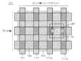
なお、図36は、複数の図35のMONOSトランジスタで構成された不揮発性メモリ101の上面図である。この不揮発性メモリ101においては、ソース領域111sおよびドレイン領域111dを含むソース/ドレイン領域111がビット線として機能し、ゲート電極130がワード線として機能する。なお、図36中のメモリセルCLの部分における断面を示したのが図35であり、メモリセルCL中のデータ蓄積領域DRに電荷CH1がトラップされることになる。
【0006】
図37および図38はいずれも、図36に示した不揮発性メモリ101のより具体的な構造の一例を示す斜視図である。図37の不揮発性メモリ101Aでは、隣接するメモリセルCLのうちソース領域111sおよびドレイン領域111dの部分に素子分離領域140が形成されている。この素子分離領域140下のソース領域111sおよびドレイン領域111dは、複数のメモリセル間で連続しており、ビット線として機能する。また、ゲート絶縁膜120は、チャネル長方向においてメモリセルごとに区切られている。
【0007】
一方、図38の不揮発性メモリ101Bでは、図37中の素子分離領域140に相当する部分を有しない。また、ゲート絶縁膜120は、チャネル長方向においてメモリセルごとに区切られることはなく連続している。なお、図37および図38の不揮発性メモリ101A,101Bではいずれも、MONOSトランジスタ上に形成された層間絶縁膜150を、その下部構造の表示を遮らないよう透明化して図示している。
【0008】
なお、この出願の発明に関連する先行技術文献情報としては次のものがある。
【0009】
【特許文献1】
米国特許第5768192号明細書
【特許文献2】
特開2002−26149号公報
【特許文献3】
特開平5−75133号公報
【非特許文献1】
I.Bloom et al.,「NROM anew non-volatile memory technology:from
device to products」,(米国),Microelectronic Engineering 59(20
01),pp.213-223
【非特許文献2】
B.Eitan et al.,「Can NROM,a 2-bit,Trapping Storage NVM Cell,
Give a Real Challenge to Floating Gate Cells?」(米国),SSDM1999
【非特許文献3】
E.Lusky et al.,「Electron Discharge Model of Locally-Trapped
Charge in Oxide-Nitride-Oxide(ONO)Gates for NROM Non-Volatile
Semiconductor Memory Devices」(米国),SSDM2001
【非特許文献4】
T.Toyoshima et al.,「0.1μm Level Contact Hole Pattern Forma-
tion with KrF Lithography by Resolution Enhancement Lithogra-
phy Assisted by Chemical Shrink(RELACS)」IEDM1998,p.333
【非特許文献5】
J.De Blauwe et al.,「Si-Dot Non-Volatile Memory Device」(米国),
Extended Abstracts of the 2001 International Conference on
Solid State Devices and Materials,Tokyo,2001,pp.518-519
【0010】
【発明が解決しようとする課題】
図39に示すように、不揮発性メモリ101のメモリセルたるMONOSトランジスタ(図35のMONOSトランジスタと同様の構造であるが、さらにサイドウォール絶縁膜160を備えている)のチャネル長がスケーリングの進行(素子の微細化)により短くなったとしても、トラップされた電荷CH1の誘起する電界EF1の実効的な範囲は変わることがない。
【0011】
さて、このMONOSトランジスタにおいては、シリコン窒化膜122中のドレイン領域111d側にだけ電荷CH1をトラップさせるだけではなく、ソース領域111s側にも電荷をトラップさせることが可能である。そこで、ソース/ドレインのそれぞれの側に電荷をトラップさせれば、一つのメモリセルで2ビットの情報を保持することが可能となる。
【0012】
図40のうち上側のMONOSトランジスタは、ソース/ドレインのそれぞれの側に電荷をトラップさせた場合を示している。ここでは、ドレイン領域111d側にトラップさせた電荷CH1をbit1と表示し、ソース領域111s側にトラップさせた電荷CH2をbit2と表示している。
【0013】
さて、図40のうち下側に示すように、ソース/ドレインの両側に電荷をトラップさせる場合も、スケーリングによりチャネル長が短くなる。このとき、ソース/ドレインのそれぞれの側に電荷をトラップさせようとすると、最初にトラップされた電荷CH1の誘起する電界EF1の斥力により、電荷CH2のトラップが妨げられる場合がある(図40中の電荷CH2a)。よって、従来の半導体装置の構造のままでは、スケーリングが進んだときに、一つのメモリセルに多ビットの情報を保持させることが困難となる。
【0014】
そこで、この発明の課題は、不揮発性メモリのスケーリングが進んだ場合にも、一つのメモリセルに多ビットの情報を保持させることが可能な半導体装置およびその製造方法を提供することにある。
【0015】
【課題を解決するための手段】
請求項1に記載の発明は、表面に溝を有する半導体基板と、前記半導体基板内において前記表面に面して形成されたソース領域、前記ソース領域とは前記溝を介して離隔して形成され、前記半導体基板内において前記表面に面して形成されたドレイン領域、前記表面のうち少なくとも前記ソース領域と前記ドレイン領域とに挟まれた部分の上に、前記溝に入り込むように形成されたゲート絶縁膜、および、前記ゲート絶縁膜上に、前記溝に入り込むように形成されたゲート電極を含むMIS(Metal Insulator Semiconductor)トランジスタとを備え、前記ゲート絶縁膜中には、電荷を保持するように構成された第1および第2の電荷保持部が前記溝を挟むように形成されており、前記ゲート絶縁膜のうち前記溝に入り込んだ部分には、前記第1および第2の電荷保持部は形成されない半導体装置である。
【0016】
請求項2に記載の発明は、請求項1に記載の半導体装置であって、前記ゲート絶縁膜は、第1のシリコン酸化膜、シリコン窒化膜、および、第2のシリコン酸化膜の順に積層された積層膜であって、前記第1および第2の電荷保持部とは、前記シリコン窒化膜のうち前記溝を挟む、互いに対向する第1および第2の部分である半導体装置である。
【0018】
請求項3に記載の発明は、請求項1に記載の半導体装置であって、前記半導体基板上には、他のソース領域、他のドレイン領域、他のゲート絶縁膜および他のゲート電極を有する他のMISトランジスタも形成されている半導体装置である。
【0019】
請求項4に記載の発明は、請求項3に記載の半導体装置であって、前記ゲート絶縁膜のうち前記溝に入り込んだ部分には、前記第1および第2の電荷保持部は形成されず、かつ、前記他のMISトランジスタの前記他のゲート絶縁膜が延在して形成されている半導体装置である。
【0020】
請求項5に記載の発明は、請求項1に記載の半導体装置であって、前記第1および第2の電荷保持部は、前記ソース領域および前記ドレイン領域上に端部を有する半導体装置である。
【0021】
請求項6に記載の発明は、請求項5に記載の半導体装置であって、前記第1および第2の電荷保持部の前記端部には、前記端部を覆う絶縁膜が形成された半導体装置である。
【0022】
請求項7に記載の発明は、請求項1に記載の半導体装置であって、前記溝の上端部および底部の角部分は丸められている半導体装置である。
【0023】
請求項8に記載の発明は、請求項1に記載の半導体装置であって、前記第1および第2の電荷保持部は、前記ゲート絶縁膜内に複数形成された島状領域である半導体装置である。
【0024】
請求項9に記載の発明は、請求項8に記載の半導体装置であって、前記島状領域は、シリコンまたはシリコン窒化膜で構成される半導体装置である。
【0025】
請求項10に記載の発明は、請求項1に記載の半導体装置であって、前記第1および第2の電荷保持部は、前記溝の側面に隣接する前記ゲート絶縁膜内に形成された半導体装置である。
【0027】
【発明の実施の形態】
<実施の形態1>
本実施の形態は、チャネル部分に溝が形成され、ゲート絶縁膜中のシリコン窒化膜が電荷保持部として溝を挟むように形成された構造のMONOSトランジスタを備える半導体装置である。
【0028】
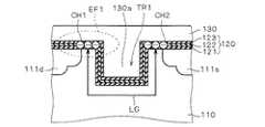
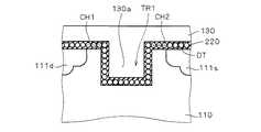
図1は、本実施の形態に係る半導体装置の備えるMONOSトランジスタを示す図である。図1に示すように、このMONOSトランジスタは、シリコン基板等の半導体基板110内に形成されたソース領域111sおよびドレイン領域111dと、半導体基板110上に形成されたゲート絶縁膜120と、ゲート絶縁膜120上に形成されたゲート電極130とを備える。このうちゲート絶縁膜120は、シリコン酸化膜121、シリコン窒化膜122およびシリコン酸化膜123の順に積層された積層膜である。
【0029】
さて、本実施の形態においては、半導体基板110の表面のうちソース領域111sおよびドレイン領域111d間のチャネル部分に、溝TR1が形成されている。また、ゲート絶縁膜120およびゲート電極130は、いずれも溝TR1に入り込むように形成されている。そして、シリコン窒化膜122のうち、溝TR1を挟む、互いに対向するソース側部分およびドレイン側部分が、電荷CH1,CH2を保持することが可能な第1および第2の電荷保持部として機能する。
【0030】
このように、チャネル中央付近に溝TR1を形成し、溝TR1内にゲート電極130が入り込むように形成されておれば、第1の電荷保持部に電荷CH1をトラップさせた後に第2の電荷保持部に電荷CH2をトラップさせる場合に、ゲート電極のうち溝TR1内の部分130aがシールドの役割を果たす。
【0031】
MONOSトランジスタにプログラム動作およびイレース動作を行う場合は、ゲート電極130に例えば0[V]や3[V]といった固定電位が与えられる。これにより、第1の電荷保持部の電荷CH1の誘起する電界EF1の影響が第2の電荷保持部に及ぶことがなく、スケーリングが進んだ場合であっても第2の電荷保持部への電荷CH2のトラップが妨げられることがないからである。
【0032】
よって、このMONOSトランジスタを不揮発性メモリのメモリセルに適用すれば、不揮発性メモリのスケーリングが進んだ場合にも、一つのメモリセルに多ビットの情報を保持させることが可能な半導体装置を実現できる。もちろん、図1に記載のMONOSトランジスタを複数、半導体基板110上に形成し、図36〜図38のようにアレイ状に配置すれば、複数のメモリセルからなる不揮発性メモリを構成できる。
【0033】
メモリセルとして、このMONOSトランジスタにプログラム動作およびイレース動作を行う場合は、図35に示したのと同様にして、半導体基板110、ゲート電極130、ソース領域111sおよびドレイン領域111dの各部に適当な電圧を印加することにより行えばよい。なお、ソース領域111sおよびドレイン領域111dの電位を浮遊状態とし、ゲート電極130と半導体基板110との間に所定の電位差を与えれば、第1および第2の電荷保持部にトラップされた電荷CH1,CH2を一括してゲート電極130もしくはチャネル側の半導体基板110に引き抜くことが可能であり、一括消去時に便利となる。また、トラップさせる電荷CH1,CH2は電子に限られるわけではなく、例えば正孔であってもよい。
【0034】
なお、ソース領域111sおよびドレイン領域111d間に溝TR1が形成されているので、実効チャネル長LGが大きくなり、パンチスルーへの耐性も向上する。
【0035】
<実施の形態2>
本実施の形態は、実施の形態1に係る半導体装置の製造方法の一例である。
【0036】
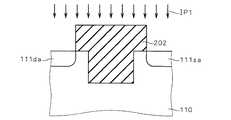
まず、図2に示すように、半導体基板110上に、フォトレジストやシリコン酸化膜、シリコン窒化膜等のマスク201を形成し、これに開口部OP1を設けて半導体基板110の表面に溝TR1を異方性エッチングにより形成する。
【0037】
次に、ウェル形成やチャネルドープなどを行う。その後、図3に示すように、フォトレジスト等のマスク202を形成して、LDD(Lightly Doped Drain)領域111sa,111daを不純物注入IP1により、半導体基板110内において表面に面した位置に、両者間に溝TR1を挟むようにして形成する。この後、同様にしてLDD領域111sa,111daよりも高濃度の不純物注入を行って、ソース領域111sおよびドレイン領域111dを形成する。
【0038】
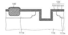
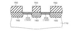
そして、半導体基板110上にゲート絶縁膜120を形成する(図4)。ここで、ゲート絶縁膜120は、シリコン酸化膜121、シリコン窒化膜122、および、シリコン酸化膜123の順に積層された積層膜であるが、本実施の形態においては、シリコン窒化膜122を素子分離領域140形成用のマスクとして用いる。
【0039】
すなわち、シリコン酸化膜121およびシリコン窒化膜122を形成し終えた段階で、フォトリソグラフィ技術およびエッチング技術によりシリコン酸化膜121およびシリコン窒化膜122にパターニングを施す。そして、パターニングされたシリコン酸化膜121およびシリコン窒化膜122をマスクとして用いて、ソース領域111sおよびドレイン領域111d内に、素子分離領域140を例えばLOCOS(LOCal Oxidation of Silicon)法等により形成する。そして、半導体基板110上の全面にシリコン酸化膜123を形成する。
【0040】
なお、素子分離領域140の形成工程の後に別工程としてシリコン酸化膜123を形成してもよいし、あるいは素子分離領域140をLOCOS法で形成する際にシリコン窒化膜122の表面が同時に熱酸化される場合には、素子分離領域140とシリコン酸化膜123とを一つの酸化工程で形成してもよい。例えばランプ酸化法の一種たるISSG(In-Situ Steam Generation)によれば、素子分離領域140とシリコン酸化膜123とを一工程内で形成することが可能である。
【0041】
その後、ゲート絶縁膜123上にゲート電極130を形成すれば、実施の形態1において示したMONOSトランジスタが完成する。
【0042】
このようにすれば、実施の形態1に係る半導体装置を製造することができる。また、シリコン酸化膜121およびシリコン窒化膜122をマスクとして用いて素子分離領域140を形成するので、新たにマスク形成することなく素子分離領域140をゲート絶縁膜120の形成途中に形成できる。よって、製造工程が簡略化でき、低コスト化が図れる。
【0043】
なお、本実施の形態においては、LDD領域111sa,111daの形成を先に行った後、ソース領域111sおよびドレイン領域111dを形成する場合について説明した。
【0044】
しかし、ソース領域111sおよびドレイン領域111dの形成後に、LDD領域111sa,111daの形成を行っても良い。
【0045】
その場合には、半導体基板110上にフォトレジスト等のマスクを形成して、まずLDD領域を含まないソース領域およびドレイン領域が形成されるようそのマスクをパターニングする。その後に不純物注入を行って、比較的高濃度のソース領域およびドレイン領域を形成する。
【0046】
次に、そのマスクのサイズをレジストアッシング等により必要な分だけシュリンクさせる(小さくする)。その後、不純物注入を行って、比較的低濃度のLDD領域を形成する。
【0047】
このようにすれば、ソース領域111sおよびドレイン領域111dの形成後に、LDD領域111sa,111daの形成が行える。
【0048】
なお、先述の場合と同様、LDD領域111sa,111daの形成を先に行った後、ソース領域111sおよびドレイン領域111dを形成する場合の他の例としては、RELACS(Resolution Enhancement Lithography Assisted by Chemical Shrink)技術を利用した方法が考えられる(RELACS技術については、上記非特許文献4を参照のこと)。
【0049】
すなわちこの場合は、半導体基板110上にフォトレジスト等のマスクを形成して、まずLDD領域が形成されるようそのマスクをパターニングする。その後に不純物注入を行って、比較的低濃度のLDD領域を形成する。
【0050】
次に、そのマスクのサイズをRELACS技術により必要な分だけ拡大させる(大きくする)。その後、不純物注入を行って、比較的高濃度のソース領域およびドレイン領域を形成する。
【0051】
このようにすれば、LDD領域111sa,111daの形成後に、ソース領域111sおよびドレイン領域111dの形成が行える。
【0052】
また、上記においては、マスクとしてフォトレジストを採用する場合を示したが、下地や周りに露出している材料とのエッチング選択比が確保できる材料であれば、シリコン酸化膜やシリコン窒化膜、ポリシリコン等もマスクに採用してよい。
【0053】
これらの材料を用いて、ソース領域111sおよびドレイン領域111dの形成後に、LDD領域111sa,111daの形成を行う場合には、シュリンク時に等方性エッチングを採用すればよい。また、逆に、LDD領域111sa,111daの形成後に、ソース領域111sおよびドレイン領域111dの形成を行う場合には、マスクサイズ拡大時にマスクと同じ材料の堆積とエッチバックとを行ってサイドウォール形成を行えばよい。
【0054】
マスクの材料には、下地材料や前後の工程を考慮して、適切なものを選択すればよい。
【0055】
また、本実施の形態においては、図4に示したようにシリコン窒化膜122を素子分離領域140形成用のマスクとして用いたが、もちろん素子分離領域140形成用のマスクはシリコン窒化膜122に限られるわけではない。
【0056】
すなわち、一般的に行われるように、半導体基板110上にフォトレジストを形成し、これをパターニングしてマスクとし、素子分離領域140をLOCOS法等にて形成してもよい。
【0057】
また、溝TR1を先に形成し、素子分離領域140を後に形成することも必須ではない。よって、素子分離領域140を予め形成した半導体基板110を用意し、その基板に溝TR1を形成してもよい。
【0058】
ただし、本実施の形態のように、溝TR1を先に、素子分離領域140を後に形成して、ゲート絶縁膜120中のシリコン窒化膜122を素子分離領域140形成用のマスクとして用いれば、無駄な工程が省けるという利点がある。
【0059】
<実施の形態3>
本実施の形態は、実施の形態1に係る半導体装置の製造方法の他の一例である。
【0060】
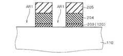
まず、半導体基板110上にダミー膜(例えばシリコン酸化膜)203を形成し、その上にさらにダミー膜203に対してエッチング選択性を有する第1のマスク膜(例えばシリコン窒化膜)204を形成する(図5)。なお、図5〜図13においてダミー膜203の符号に(120)と並記しているのは、実施の形態7においてもこれらの図を用いるためであり、本実施の形態においては(120)との並記部分は無視してよい。
【0061】
次に、フォトレジスト205を形成し、これにパターニングを行って開口部OP2を設ける(図6)。そして、ダミー膜203および第1のマスク膜204に異方性エッチングを施す。これにより素子分離領域が形成されるべき領域AR1に開口部が形成される(図7)。
【0062】
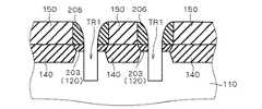
続いて、フォトレジスト205を除去し、領域AR1の開口部に露出する半導体基板110の表面に素子分離領域140を例えばLOCOS法等により形成する(図8)。そして、第1のマスク膜204に対してエッチング選択性を有する層間絶縁膜(例えばシリコン酸化膜)150を、半導体基板110上の全面に形成して、その表面をCMP(Chemical Mechanical Polishing)で研磨し、第1のマスク膜204を露出させる。これにより、層間絶縁膜150が領域AR1の開口部内に埋め込まれる(図9)。そして、エッチング選択性を利用して、層間絶縁膜150およびダミー膜203を残しつつ第1のマスク膜204をエッチングにより除去する(図10)。
【0063】
次に、層間絶縁膜150およびダミー膜203上に、この両者に対してエッチング選択性を有する第2のマスク膜(例えばシリコン窒化膜)を形成して、これにエッチバックを施すことにより、第1のマスク膜204の除去部分においてサイドウォール膜206を形成する(図11)。
【0064】
そして、層間絶縁膜150およびサイドウォール膜206をマスクとしつつエッチングを行い、溝TR1を形成する(図12)。その後、溝TR1内にサイドウォール膜206に対してエッチング選択性を有するSOG(Spin On Glass)207を埋め込む(図13)。
【0065】
続いて、エッチング選択性を利用して、SOG207、ダミー膜203および層間絶縁膜150を残しつつサイドウォール膜206をエッチングにより除去する。そして、SOGを除去する(図14)。SOGは、熱酸化法等で形成されたシリコン酸化膜に比べてエッチング速度が速いという特性を有している。よって、SOGを用いることで、層間絶縁膜150およびダミー膜203を残しつつSOG207だけを除去することが可能である。
【0066】
これにより半導体基板110に溝TR1が形成された状態となるので、この後、ダミー膜203を除去すれば、実施の形態2における図3以降の工程を行うことで、実施の形態1に係る半導体装置を製造することが可能となる。
【0067】
本実施の形態によれば、層間絶縁膜150およびサイドウォール膜206をマスクとしつつ溝TR1を形成し、その後、サイドウォール膜206、SOG207およびダミー膜203を除去する。よって、素子分離領域140を形成した後に溝TR1を形成することができる。
【0068】
<実施の形態4>
本実施の形態は、実施の形態1に係る半導体装置の変形例であって、ゲート絶縁膜120のうち溝TR1に入り込んだ部分には、電荷保持部たるシリコン窒化膜122が形成されない構造のMONOSトランジスタを備える半導体装置である。
【0069】
図15は、本実施の形態に係る半導体装置の備えるMONOSトランジスタを示す図である。図15に示すように、このMONOSトランジスタにおいては、溝TR1内にはゲート絶縁膜120が形成されず、その代わりに新たなゲート絶縁膜(例えばシリコン酸化膜)124が形成されている。その他の構成は図1に示したMONOSトランジスタと同様のため、説明を省略する。
【0070】
このように、ゲート絶縁膜120のうち溝TR1に入り込んだ部分に、電荷保持部たるシリコン窒化膜122が形成されていなければ、溝TR1部分のゲート絶縁膜124の膜厚を薄くすることができる。よって、溝TR1部分におけるチャネル生成に必要なゲート電圧の値を低く抑えることができる。
【0071】
また、図16に示すように、半導体基板110上に、ソース領域211s、ドレイン領域211d、ゲート絶縁膜125、ゲート電極230、およびサイドウォール絶縁膜231を有する他のMISトランジスタも形成されておれば、図15の新たなゲート絶縁膜124の代わりに、ゲート絶縁膜125を溝TR1内に延在して形成してもよい。
【0072】
半導体基板110上に他のMISトランジスタが形成されておれば、MONOSトランジスタを例えばメモリセルに用い、他のMISトランジスタを論理回路の構成素子に用いるシステムLSI(Large Scale Integration)として構成することが可能である。
【0073】
そして、他のMISトランジスタのゲート絶縁膜125を溝TR1内に延在して形成することで、MONOSトランジスタのゲート絶縁膜のうち溝TR1に入り込んだ部分の材質を、他のゲート絶縁膜125の材質と同じくすることができ、例えば高誘電率絶縁膜を溝TR1部分に採用することが可能となる。
【0074】
<実施の形態5>
本実施の形態は、実施の形態4に係る半導体装置の製造方法の一例である。
【0075】
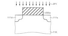
まず、図17に示すように、溝TR1の形成に先立って半導体基板110上に、シリコン酸化膜121、シリコン窒化膜122、およびシリコン酸化膜を順に積層し、ゲート絶縁膜120を形成する。そして、ゲート絶縁膜120上にフォトレジスト等のマスク208を形成し、これに開口部OP3を設ける。
【0076】
そして、ゲート絶縁膜120のうち開口部OP3に露出する部分をもエッチングしつつ、異方性エッチングにより半導体基板110の表面に溝TR1を形成する。その後、マスク208を除去し、必要であればチャネル部分に斜め回転注入法により不純物注入IP2を行う(図18)。なお、しきい値電圧の設定如何によって、不純物注入IP2を行うかどうかを決定すればよい。
【0077】
次に、溝TR1内に新たなゲート絶縁膜124を形成する(図19)。ゲート絶縁膜124をシリコン酸化膜で構成する場合には、熱酸化法やランプ酸化法(あるいはRTO法:Rapid Thermal Oxidation Method)を採用すればよい。
【0078】
この後、図20に示すように、フォトレジスト等のマスク202を形成して、LDD領域111sa,111daを不純物注入IP1により、半導体基板110内において表面に面した位置に、両者間に溝TR1を挟むようにして形成する。この後、同様にしてLDD領域111sa,111daよりも高濃度の不純物注入を行って、ソース領域111sおよびドレイン領域111dを形成する。
【0079】
その後、マスク202を除去してゲート絶縁膜120上にゲート電極130を形成すれば、図15に示すMONOSトランジスタを製造することができる。
【0080】
なお、図37のような素子分離領域140を有する構造を製造する場合には、例えば図17の段階よりも前に、シリコン酸化膜121およびシリコン窒化膜122を形成し終えた段階で、フォトリソグラフィ技術およびエッチング技術によりシリコン酸化膜121およびシリコン窒化膜122にパターニングを施しておく。そして、パターニングされたシリコン酸化膜121およびシリコン窒化膜122をマスクとして用いて、素子分離領域140を例えばLOCOS法等により形成しておけばよい。また、素子分離領域140の形成前にソース領域111sおよびドレイン領域111dを形成しておいてもよい。
【0081】
また、図16に示すMONOSトランジスタを製造する場合には、例えば図18の段階後にゲート絶縁膜125を半導体基板110上の全面に形成し、その後、ソース/ドレインの形成を経て、ゲート電極130、230を一つのパターニングプロセスで形成すればよい。
【0082】
なお、LDD領域とソース/ドレインの形成の先後については、実施の形態2において説明したように、いずれであってもよい。
【0083】
<実施の形態6>
本実施の形態は、実施の形態4に係る半導体装置の製造方法の他の一例である。なお、本実施の形態では、図37のような素子分離領域140を有する構造を製造する場合を想定している。
【0084】
まず、半導体基板110上にシリコン酸化膜121およびシリコン窒化膜122を形成する。その後、シリコン窒化膜122上にフォトレジスト等のマスク209を形成し、素子分離領域140を形成する領域が開口するよう開口部OP4をマスク209に設ける(図21)。
【0085】
次に、マスク209を用いて開口部OP4に露出するシリコン酸化膜121およびシリコン窒化膜122をエッチングにより除去し、マスク209を除去する。そして、不純物注入IP3を行い(図22)、半導体基板110内にソース領域111sbおよびドレイン領域111dbを形成する。
【0086】
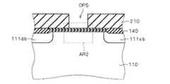
続いて、シリコン酸化膜121およびシリコン窒化膜122をマスクとして用いて、ソース領域111sbおよびドレイン領域111db内に、素子分離領域140を例えばLOCOS法等により形成する(図23)。その後、シリコン窒化膜122および素子分離領域140上にフォトレジスト等のマスク210を形成し、これに開口部OP5を設ける(図24)。
【0087】
次に、シリコン酸化膜121およびシリコン窒化膜122のうち開口部OP5に露出する部分をもエッチングしつつ、異方性エッチングにより半導体基板110の表面に溝TR1を形成する。そして、マスク210を除去し、必要であればチャネル部分に斜め回転注入法により不純物注入IP2を行う(図25)。しきい値電圧の設定如何によって、不純物注入IP2を行うかどうかを決定すればよい。なお、図25は、図24内の領域AR2を拡大表示したものである。
【0088】
その後、半導体基板110上の全面に、熱酸化法等によりシリコン酸化膜123および124を形成し(図26)、ゲート絶縁膜123および124上にゲート電極130を形成する。このようにすれば、図15に示すMONOSトランジスタを製造することができる。また、図16に示すMONOSトランジスタを製造する場合には、例えば図26においてシリコン酸化膜123および124の代わりに、他のMISトランジスタのゲート絶縁膜125を形成してもよい。
【0089】
このようにすれば、実施の形態2におけると同様、シリコン酸化膜121およびシリコン窒化膜122をマスクとして用いて素子分離領域140を形成するので、新たにマスク形成することなく素子分離領域140をゲート絶縁膜120の形成途中に形成できる。よって、製造工程が簡略化でき、低コスト化が図れる。
【0090】
もちろん、実施の形態2において説明したように、素子分離領域140形成用のマスクはシリコン窒化膜122に限られるわけではない。そして、溝TR1の形成を素子分離領域140の形成後に行うことも必須ではない。
【0091】
<実施の形態7>
本実施の形態も、実施の形態4に係る半導体装置の製造方法の他の一例である。なお、本実施の形態は、実施の形態3におけるダミー膜203の代わりに、ゲート絶縁膜120を最初から形成しておくようにした製造方法である。よって、実施の形態3において示された図5〜図13を用いて説明を行うが、以下では、図5〜図13において、ダミー膜203に代わってゲート絶縁膜120が形成されているものとする。
【0092】
まず、半導体基板110上に、シリコン酸化膜121、シリコン窒化膜122およびシリコン酸化膜123の積層膜たるゲート絶縁膜120を形成する。そして、その上にさらにシリコン酸化膜123に対してエッチング選択性を有する第1のマスク膜(例えばシリコン窒化膜)204を形成する(図5)。
【0093】
次に、フォトレジスト205を形成し、これにパターニングを行って開口部OP2を設ける(図6)。そして、ゲート絶縁膜120および第1のマスク膜204に異方性エッチングを施す。これにより素子分離領域が形成されるべき領域AR1に開口部が形成される(図7)。
【0094】
続いて、フォトレジスト205を除去し、領域AR1の開口部に露出する半導体基板110の表面に素子分離領域140を例えばLOCOS法等により形成する(図8)。そして、第1のマスク膜204に対してエッチング選択性を有する層間絶縁膜(例えばシリコン酸化膜)150を、半導体基板110上の全面に形成して、その表面をCMP(Chemical Mechanical Polishing)で研磨し、第1のマスク膜204を露出させる。これにより、層間絶縁膜150が領域AR1の開口部内に埋め込まれる(図9)。そして、エッチング選択性を利用して、層間絶縁膜150およびゲート絶縁膜120を残しつつ第1のマスク膜204をエッチングにより除去する(図10)。
【0095】
次に、層間絶縁膜150およびシリコン酸化膜123上に、この両者に対してエッチング選択性を有する第2のマスク膜(例えばシリコン窒化膜)を形成して、これにエッチバックを施すことにより、第1のマスク膜204の除去部分においてサイドウォール膜206を形成する(図11)。
【0096】
そして、層間絶縁膜150およびサイドウォール膜206をマスクとしつつエッチングを行い、溝TR1を形成する(図12)。その後、溝TR1内にサイドウォール膜206に対してエッチング選択性を有するSOG207を埋め込む(図13)。
【0097】
続いて、エッチング選択性を利用して、SOG207、ゲート絶縁膜120および層間絶縁膜150を残しつつサイドウォール膜206をエッチングにより除去する。そして、SOGを除去する。この状態を示すのが図27である。これにより半導体基板110に溝TR1およびゲート絶縁膜120が形成された状態となるので、実施の形態5における図18以降の工程を行うことで、実施の形態4に係る半導体装置を製造することが可能となる。
【0098】
本実施の形態によれば、層間絶縁膜150およびサイドウォール膜206をマスクとしつつ溝TR1を形成し、その後、サイドウォール膜206、SOG207を除去する。よって、素子分離領域140を形成した後に溝TR1を形成することができる。
【0099】
<実施の形態8>
本実施の形態は、実施の形態4に係る半導体装置の変形例であって、ゲート絶縁膜120のうち第1および第2の電荷保持部たるシリコン窒化膜122が、ソース領域111sおよびドレイン領域111d上に端部を有する構造のMONOSトランジスタを備える半導体装置である。
【0100】
図28は、本実施の形態に係る半導体装置の備えるMONOSトランジスタを示す図である。図28に示すように、このMONOSトランジスタにおいては、シリコン窒化膜122およびその上のシリコン酸化膜123がソース領域111sおよびドレイン領域111d上で終端している。その他の構成は図15に示したMONOSトランジスタと同様のため、説明を省略する。
【0101】
このように、シリコン窒化膜122がソース領域111sおよびドレイン領域111d上で終端しておれば、このMONOSトランジスタが連続して複数のメモリセルとして形成され、隣接するトランジスタ間でゲート絶縁膜120内のシリコン酸化膜121を共有する場合であっても、メモリセルごとに第1および第2の電荷保持部が絶縁される。よって、メモリセル間で電荷CH1,CH2の移動が生じることはない。
【0102】
シリコン窒化膜122にトラップされた電荷が移動することは考えにくいが、メモリセルごとに第1および第2の電荷保持部を絶縁しておくことで、電荷CH1,CH2の移動範囲を確実に限定することが可能となる。これにより、MONOSトランジスタのしきい値分布の広がりも抑制することができる。
【0103】
なお、図29に示すように、第1および第2の電荷保持部たるシリコン窒化膜122の終端部分には、終端部分を覆う絶縁膜(例えばシリコン酸化膜)126が形成されていてもよい。これにより、ゲート電極130がシリコン窒化膜122の終端部分にまで延在している場合であっても、シリコン窒化膜122に保持された電荷CH1,CH2がゲート電極130内に移動することを防止できる。
【0104】
<実施の形態9>
本実施の形態は、実施の形態8に係る半導体装置の製造方法の一例である。
【0105】
本実施の形態においては、実施の形態5に係る半導体装置の製造方法と同様にして、図17〜図19に示す工程を行う。この後、図30に示すように、フォトレジスト等のマスク202を形成して、LDD領域111sa,111daの形成領域を開口する。そして、開口した部分のシリコン酸化膜123およびシリコン窒化膜122をエッチングにより除去し、電荷保持部がソース領域およびドレイン領域上で終端するようにする。
【0106】
この後、マスク202を残したまま不純物注入IP1を行ってLDD領域111sa,111daを形成する。この後、同様にしてLDD領域111sa,111daよりも高濃度の不純物注入を行って、ソース領域111sおよびドレイン領域111dを形成する。
【0107】
その後、マスク202を除去してゲート絶縁膜120上にゲート電極130を形成すれば、図28に示すMONOSトランジスタを製造することができる。
【0108】
なお、図29に示すMONOSトランジスタを製造する場合には、図30の段階の後にマスク202を除去し、例えば熱酸化を行って、電荷保持部たるシリコン窒化膜122の終端部分にこれを覆う絶縁膜126を形成すればよい。
【0109】
なお、LDD領域とソース/ドレインの形成の先後については、実施の形態2において説明したように、いずれであってもよい。
【0110】
<実施の形態10>
本実施の形態は、実施の形態1に係る半導体装置の変形例であって、溝TR1の上端部および底部の角部分が丸められている構造のMONOSトランジスタを備える半導体装置である。
【0111】
図31は、本実施の形態に係る半導体装置の備えるMONOSトランジスタを示す図である。図31に示すように、このMONOSトランジスタにおいては、溝TR1の上端部および底部の角部分CR1,CR2が丸められている。その他の構成は図1に示したMONOSトランジスタと同様のため、説明を省略する。
【0112】
このように、溝TR1の上端部および底部の角部分CR1,CR2が丸められておれば、角部分における電界の集中を抑制でき、半導体装置の信頼性を向上させることができる。
【0113】
<実施の形態11>
本実施の形態は、実施の形態10に係る半導体装置の製造方法の一例である。
【0114】
本実施の形態においては、実施の形態2に係る半導体装置の製造方法と同様にして、図2に示す工程を行い、溝TR1を半導体基板110内に形成する。この後、図32に示すように、溝TR1の表面に例えばシリコン酸化膜等からなる犠牲層211を形成する。犠牲層211の形成は、例えば熱酸化法を用いればよい。
【0115】
その後、犠牲層211を例えばフッ酸を用いたウェットエッチングにより除去する。これにより、図33に示すように、溝TR1の上端部および底部の角部分CR1,CR2が丸められる。この後、実施の形態2と同様にして図3以降の工程を行なえば、図31に示すMONOSトランジスタを製造することができる。
【0116】
<実施の形態12>
本実施の形態も、実施の形態1に係る半導体装置の変形例であり、ゲート絶縁膜に、シリコン窒化膜を含む積層構造を採用せずに、シリコンで形成された複数の島状領域たるドットを有するゲート絶縁膜を採用する場合を示すものである。
【0117】
シリコン酸化膜内にシリコンのドットを形成する技術が、例えば上記非特許文献5に記載されている。本実施の形態においては、ゲート絶縁膜にこのようなシリコンドットを含むシリコン酸化膜を採用する。
【0118】
図34は本実施の形態に係る半導体装置の備えるMISトランジスタを示す図である。図34では、ゲート絶縁膜120が、シリコンドットDTを含む単層構造のゲート絶縁膜(例えばシリコン酸化膜)220に置換されていること以外は、実施の形態1に係る半導体装置と同様の構造である。
【0119】
実施の形態1の場合、電荷CH1,CH2が保持されるのはシリコン窒化膜122中のトラップ準位であるが、このトラップ準位はシリコン窒化膜122内の欠陥部分に存在しているため、トラップ準位の値が場所により不均一である。そのため、保持した電荷CH1,CH2を長期間保存した場合に、エネルギーの揺らぎなどがあれば電荷CH1,CH2が抜け出てしまう可能性がある。特に、浅い準位にトラップされた電荷は、深い準位にトラップされた電荷に比べて飛び出してしまいやすい。
【0120】
シリコンドットDTの場合は、導電性があることからトラップ準位がシリコン窒化膜のものと比べて深く、かつ、場所に関わらず安定しているため、保持した電荷が抜ける確率が低くなる。これはすなわち、実施の形態1におけるシリコン窒化膜122のように第1および第2の電荷保持部がゲート絶縁膜120内で連続する膜である場合に比べて、保持した電荷の移動がより起こりにくく、より不揮発性に優れた半導体装置を実現できることを意味する。
【0121】
なお、シリコンドットの代わりに、シリコン窒化膜をシリコン酸化膜内にドット状に形成する技術が、例えば上記特許文献3に記載されている(当該公報の図1を参照)。シリコン窒化膜であっても、ドット状であればゲート絶縁膜120内で連続する膜である場合に比べて、保持した電荷の移動がより起こりにくく、シリコンドットDTの場合と同様の効果があると考えられる。
【0122】
<実施の形態13>
実施の形態12においては、実施の形態1におけるゲート絶縁膜120が、シリコンまたはシリコン窒化膜のドットDTを含む単層構造のゲート絶縁膜220に置換されている構造を説明した。このようなドットDTを含むゲート絶縁膜220は、上述の実施の形態2〜11の全てにおいてゲート絶縁膜120に置換して用いることが可能である。
【0123】
すなわち言い換えれば、MISトランジスタの構造であって、そのゲート絶縁膜中にONO膜やドットのような、電荷を保持することが可能な電荷保持部が形成されている構造であれば、本発明の実施の形態1〜12を適用することが可能である。
【0124】
<実施の形態14>
本実施の形態は、ゲート絶縁膜中のシリコン窒化膜を電荷保持部とし、チャネル中央部上のゲート絶縁膜を下層のシリコン酸化膜のみとした構造のMONOSトランジスタを備える半導体装置である。
【0125】
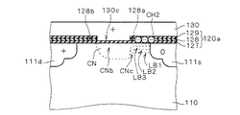
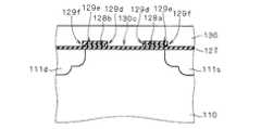
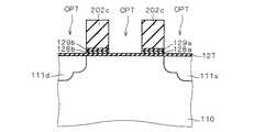
図41は、本実施の形態に係る半導体装置の備えるMONOSトランジスタを示す図である。図41に示すように、このMONOSトランジスタは、シリコン基板等の半導体基板110内に形成されたソース領域111sおよびドレイン領域111dと、半導体基板110上に形成されたゲート絶縁膜120aと、ゲート絶縁膜120a上に形成されたゲート電極130とを備える。
【0126】
このうちゲート絶縁膜120aは、チャネル中央部上以外の部分においては、シリコン酸化膜127、シリコン窒化膜128およびシリコン酸化膜129の順に積層された積層膜である。なお、チャネル中央部上においては、ゲート絶縁膜120aは、シリコン酸化膜127の延在した部分127aのみで構成されている。
【0127】
さて、本実施の形態においては、ソース領域111sおよびドレイン領域111dを結ぶ方向に互いに対向しつつ離隔して形成されたシリコン窒化膜128が、電荷CH1、CH2を保持可能な第1および第2の電荷保持部128b,128aとして機能する。
【0128】
そして、チャネル中央部上、すなわち、ゲート絶縁膜120aのうち第1および第2の電荷保持部128b,128aに挟まれた部分においては、ゲート絶縁膜120aは上述のようにシリコン酸化膜127の延在した部分127aのみで構成されている。よって、その部分の膜厚は、第1および第2の電荷保持部128b,128aが形成された積層膜部分の膜厚よりも小さい。また、第1および第2の電荷保持部128b,128aの間には、ゲート電極130のチャネル中央部上の部分130cが介在する。より具体的には、第1および第2の電荷保持部128b,128aの端部が、ゲート電極130のチャネル中央部上の部分130cと面130bで接している。
【0129】
図42は、本実施の形態に係る半導体装置において情報を保持させる場合を示す図である。また、図43は、本実施の形態に係る半導体装置において情報を読み取る場合を示す図である。
【0130】
図42においては、ドレイン領域111dに接地電位0[V](「0」と表示)を与え、ソース領域111sおよびゲート電極130に接地電位よりも高い電位(いずれも「+」と表示)を与えて半導体基板110内にチャネルCNを形成し、情報の書き込みを行う様子を示している。なお、接地電位を基準として例えば、ソース領域111sに与える電位を5[V]、ゲート電極130に与える電位を9[V]とすればよい。
【0131】
第1および第2の電荷保持部128b,128aの形成された部分は積層膜となっており、ゲート絶縁膜120aの膜厚が大きい。よって、積層膜直下においては、ゲート電極130への電圧印加より半導体基板110内にチャネルCNaは浅く形成される。
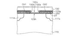
【0132】
また、チャネル中央部上においては、シリコン酸化膜127の延在部127aのみとなっており、ゲート絶縁膜120aの膜厚が小さい。よって、チャネル中央部内においては、ゲート電極130への電圧印加より半導体基板110内にチャネルCNbが深く形成される。
【0133】
各部への電圧印加により、電荷(例えば電子)CH2は、加速しつつドレイン領域111dからソース領域111sに向かって、チャネルホットエレクトロンとして移動する。そして、チャネルCNのピンチオフ点PN付近で第2の電荷保持部128aにトラップされる。
【0134】
一方、図43においては、ソース領域111sに接地電位0[V](「0」と表示)を与え、ドレイン領域111dおよびゲート電極130に接地電位よりも高い電位(いずれも「+」と表示)を与えて半導体基板110内にチャネルCNを形成し、情報の読み出しを行う様子を示している。なお、接地電位を基準として例えば、ドレイン領域111dに与える電位を1.6[V]、ゲート電極130に与える電位を3.5[V]とすればよい。
【0135】
第2の電荷保持部128aにトラップされた電荷CH2の多寡に応じて、第2の電荷保持部128a下の半導体基板110内に形成されるチャネルCNcの深さはLB1〜LB3に示すように異なる。この深さLB1〜LB3の違いにより、MONOSトランジスタのしきい値電圧に変化が生じ、しきい値電圧の変化を検出することにより、メモリセルに1ビットの情報が記憶されているか否かを判断できる。
【0136】
また、イレース動作を行う場合は、ゲート電極130、ソース領域111sおよびドレイン領域111dの各部に適当な電圧を印加することにより行えばよい。例えば、ドレイン領域111dに与える電位を8[V]、ゲート電極130に与える電位を0[V]とすればよい。あるいは、ドレイン領域111dに与える電位を5[V]、ゲート電極130に与える電位を−6[V]とすればよい。なお、ソース領域111sおよびドレイン領域111dの電位を浮遊状態とし、ゲート電極130と半導体基板110との間に所定の電位差を与えれば、第1および第2の電荷保持部にトラップされた電荷CH1,CH2を一括してゲート電極130もしくはチャネル側の半導体基板110に引き抜くことも可能であり、一括消去時に便利となる。
【0137】
さて、図42において第1の電荷保持部128bには電荷CH1を示していないが、もし図41のように第1の電荷保持部128bに電荷CH1が既にトラップされていた場合であっても、本実施の形態に係る半導体装置によれば、第2の電荷保持部128aへの電荷CH2のトラップを行うことができる。それは以下の理由からである。
【0138】
上述のように、チャネル中央部内においては、チャネルCNbは深く形成される。これにより、多数のチャネルホットキャリア(電子の場合はチャネルホットエレクトロン)を生み出すことができる。多数のチャネルホットキャリアが生成されることにより、第1の電荷保持部128bに電荷CH1をトラップさせた後に第2の電荷保持部128aに電荷CH2をトラップさせる場合であっても、トラップの確率を高めることができる。
【0139】
また、第1および第2の電荷保持部128b,128aの間にはゲート電極130が介在するので、第1の電荷保持部128bに電荷CH1をトラップさせた後に第2の電荷保持部128aに電荷CH2をトラップさせる場合に、ゲート電極130のチャネル中央部上の部分130cがシールドの役割を果たす。
【0140】
すなわち、上記のように本実施の形態においては、トラップの確率が高く、かつ、ゲート電極130のチャネル中央部上の部分130cがシールドの役割を果たすことから、第1の電荷保持部128bの電荷CH1の誘起する電界EF1の影響が第2の電荷保持部128aに及びにくく、スケーリングが進んだ場合であっても第2の電荷保持部128aへの電荷CH2のトラップが妨げられにくい。よって、このMISトランジスタを不揮発性メモリのメモリセルに適用すれば、不揮発性メモリのスケーリングが進んだ場合にも、一つのメモリセルに多ビットの情報を保持させることが可能な半導体装置を実現できる。もちろん、図41に記載のMONOSトランジスタを複数、半導体基板110上に形成し、図36〜図38のようにアレイ状に配置すれば、複数のメモリセルからなる不揮発性メモリを構成できる。
【0141】
なお、図41に示した、第1および第2の電荷保持部128b,128aのチャネル長方向の長さL1,L3、および、シリコン酸化膜127の延在した部分127aのチャネル長方向の長さL2については、ピンチオフ点PNの設計位置、ゲート電極130やソース領域111s、ドレイン領域111dに与えるべき動作電圧、トランジスタサイズ等に応じて適宜、設定すればよい。例えば、電荷が注入される箇所はピンチオフ点PN付近と考えられているので、第2の電荷保持部128aがピンチオフ点PN上に位置するよう、チャネル長方向の長さL3を設定すればよい。
【0142】
なお、第1および第2の電荷保持部128b,128aがいずれも、シリコン酸化膜127、シリコン窒化膜128、および、シリコン酸化膜129の順に半導体基板110上に積層された積層膜のうちのシリコン窒化膜128である。シリコン窒化膜128はシリコン酸化膜127,129に挟まれているので、シリコン窒化膜128に保持された電荷CH1,CH2がゲート電極130及び半導体基板110内に移動することを防止できる。
【0143】
また、ゲート絶縁膜120aのうち、第1および第2の電荷保持部128b,128aに挟まれた部分は、シリコン酸化膜127の延在した部分127aである。よって、積層膜内のシリコン酸化膜127をゲート絶縁膜120aの薄い膜厚部分として利用することができ、半導体装置の製造が容易である。
【0144】
なお、トラップさせる電荷CH1,CH2は電子に限られるわけではなく、例えば正孔であってもよい。
【0145】
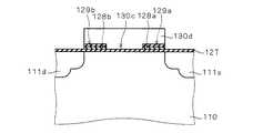
また、図41の構造に代えて、図44または図45のような構造としてもよい。両図においては、第1および第2の電荷保持部128b,128aが、ソース領域111sおよびドレイン領域111d上に端部を有している。図45では、ゲート電極についても、ソース領域111sおよびドレイン領域111d上で終端した形状130dが採用されている。
【0146】
よって、実施の形態8に係る半導体装置と同様、本実施の形態に係るMONOSトランジスタが連続して複数のメモリセルとして形成され、隣接するトランジスタ間でゲート絶縁膜を共有する場合であっても、メモリセルごとに第1および第2の電荷保持部128b,128aが絶縁される。よって、メモリセル間で電荷の移動が生じることはない。
【0147】
<実施の形態15>
本実施の形態は、実施の形態14に係る半導体装置の変形例であって、第1および第2の電荷保持部128b,128aのうち相互に対向する端部とゲート電極130との間に介在する絶縁膜を形成するものである。
【0148】
図46は、本実施の形態に係る半導体装置を示す図である。この半導体装置においては図46に示すように、図41の構造のうちシリコン酸化膜129を、第1および第2の電荷保持部128b,128aのうちゲート電極130に面する部分をも覆うシリコン酸化膜129cに変更している。具体的には、第1および第2の電荷保持部128b,128aのチャネル側終端部を、シリコン酸化膜129cの端部129dが覆っている。その他の構造は、実施の形態14に係る半導体装置と同様である。
【0149】
このように、第1および第2の電荷保持部128b,128aのうちゲート電極130に面する部分をシリコン酸化膜129cで覆えば、第1および第2の電荷保持部128b,128aに保持された電荷が、ゲート電極130内に移動することを防止できる。
【0150】
なお、図47および図48は、図44および図45の構造にシリコン酸化膜129cを適用したものである。両図においては、第1および第2の電荷保持部128b,128aのチャネル側端部を、シリコン酸化膜129eの端部129dが覆いつつ、第1および第2の電荷保持部128b,128aのソース/ドレイン側端部をも、シリコン酸化膜129eの端部129fが覆っている。その他の構造は、図44および図45と同様である。
【0151】
このように、第1および第2の電荷保持部128b,128aのソース/ドレイン側端部をもシリコン酸化膜129eで覆えば、ゲート電極130が第1および第2の電荷保持部128b,128aの端部にまで延在している場合であっても、第1および第2の電荷保持部128b,128aに保持された電荷がゲート電極130内に移動することを防止できる。
【0152】
<実施の形態16>
本実施の形態も、実施の形態14に係る半導体装置の変形例であり、ゲート絶縁膜の第1および第2の電荷保持部に、シリコン窒化膜を含む積層構造を採用せずに、シリコンで形成された複数の島状領域たるドットを有する絶縁膜を採用するものである。
【0153】
図49は本実施の形態に係る半導体装置の備えるMISトランジスタを示す図である。図49では、シリコンドットDTを含む絶縁膜(例えばシリコン酸化膜)250が、第1および第2の電荷保持部として半導体基板110上に形成されている。なお、チャネル中央部上においては、絶縁膜250は途切れている。すなわち、本実施の形態においては、ソース領域111sおよびドレイン領域111dを結ぶ方向に互いに対向しつつ離隔して形成された絶縁膜250が、電荷CH1、CH2を保持可能な第1および第2の電荷保持部として機能する。
【0154】
そして、半導体基板110のチャネル中央部表面と、絶縁膜250とを覆うシリコン酸化膜129gが、さらに形成されている。絶縁膜250が途切れていることから、チャネル中央部上のゲート絶縁膜は、シリコン酸化膜129gのチャネル上部分129hのみで構成される。一方、第1および第2の電荷保持部の形成部分のゲート絶縁膜は、絶縁膜250およびシリコン酸化膜129gの積層構造で構成される。なお、シリコン酸化膜129gの膜厚は、第1および第2の電荷保持部たる絶縁膜250の膜厚よりも小さくしておく。
【0155】
よって、チャネル中央部上、すなわち、第1および第2の電荷保持部たる絶縁膜250に挟まれた部分のゲート絶縁膜の膜厚は、第1および第2の電荷保持部が形成された積層膜部分のゲート絶縁膜の膜厚よりも小さい。また、第1および第2の電荷保持部たる絶縁膜250の間には、ゲート電極130のチャネル中央部上の部分130cが介在する。
【0156】
ゲート絶縁膜が、絶縁膜250およびシリコン酸化膜129gに置換されていること以外は、実施の形態14に係る半導体装置と同様の構造である。なお、シリコンドットDTを採用する利点は、実施の形態12における記述と同様である。また、シリコンドットの代わりに、ドット状シリコン窒化膜を採用してもよい。
【0157】
このように、第1および第2の電荷保持部を、ゲート絶縁膜内に複数形成されたドットで構成すれば、第1および第2の電荷保持部がシリコン窒化膜128のようにゲート絶縁膜内で連続する膜である場合に比べて、保持した電荷の移動がより起こりにくく、より不揮発性に優れた半導体装置を実現できる。
【0158】
また、ゲート絶縁膜に例えばシリコン酸化膜を用いる場合、シリコンまたはシリコン窒化膜のドットにおけるエネルギー準位はシリコン酸化膜のエネルギー準位よりも安定している。よって、ドットをシリコンまたはシリコン窒化膜で構成すれば、保持した電荷の移動が起こりにくく、不揮発性に優れた半導体装置を実現できる。
【0159】
<実施の形態17>
本実施の形態は、実施の形態14に係る半導体装置の製造方法の一例である。
【0160】
まず、半導体基板110内にウェル形成やチャネルドープなどを行う。次に、図50に示すように、フォトレジスト等のマスク202aを形成して、ソース領域111sおよびドレイン領域111dを不純物注入IP1により、半導体基板110内において表面に面した位置に形成する。なお、このときの不純物注入IP1の不純物濃度は、1×10¹⁴〜1×10¹⁵[/cm2]程度と設定すればよい。また、ソース領域111sおよびドレイン領域111d間の距離、すなわちチャネル長については、0.1〜0.3μm程度とすればよい。
【0161】
そして、マスク202aを除去した後、半導体基板110上にゲート絶縁膜120aを形成する(図51)。すなわち、ゲート絶縁膜120aを構成する、シリコン酸化膜127、シリコン窒化膜128、および、シリコン酸化膜129をこの順に、例えばCVD法により積層して形成する。なお、各部の膜厚については例えば、シリコン酸化膜127を2.5〜6.0nm、シリコン窒化膜128を6.0nm、シリコン酸化膜129を3.0nm、程度とすればよい。
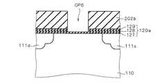
【0162】
次に、シリコン酸化膜129上に、フォトレジスト等のマスク202bを形成して、チャネル中央部上に開口部OP6を設ける。そして、これをマスクとして、フォトリソグラフィ技術およびエッチング技術によりシリコン酸化膜129およびシリコン窒化膜128にパターニングを施す(図52)。そして、マスク202bを除去し、シリコン酸化膜127,129上にポリシリコン等の導電膜をCVD法等により形成して、ゲート電極130を設ける。こうすれば、実施の形態14において示したMONOSトランジスタが完成する。
【0163】
なお、図44または図45のような構造にする場合は、図53に示すように、マスク202bに代えて、開口部OP7を有するマスク202cの形状を採用すればよい。
【0164】
また、上記においては、マスクとしてフォトレジストを採用する場合を示したが、下地や周りに露出している材料とのエッチング選択比が確保できる材料であれば、シリコン酸化膜やシリコン窒化膜、ポリシリコン等もマスクに採用してよい。
【0165】
<実施の形態18>
本実施の形態は、実施の形態15に係る半導体装置の製造方法の一例である。
【0166】
まず、実施の形態17の場合と同様にして、半導体基板110内にソース領域111sおよびドレイン領域111dを形成し、半導体基板110上にゲート絶縁膜120aを形成する。そして、シリコン酸化膜129およびシリコン窒化膜128へのパターニング後に、熱酸化法によりシリコン窒化膜128のチャネル側終端部分にこれを覆う絶縁膜を形成し、シリコン酸化膜129cの端部129dとすればよい(図54)。
【0167】
なお、実施の形態15に係る半導体装置の構造はこの他にも、例えば以下のようにして製造すればよい。すなわち、図55に示すように、図52のパターニング処理において下層のシリコン酸化膜127までエッチングを行い、その後、図56に示すように、露出したチャネル部分の半導体基板110およびシリコン窒化膜128のチャネル側終端部分を熱酸化してシリコン酸化膜129iを形成すればよい。
【0168】
あるいは、図57に示すように、シリコン酸化膜127およびシリコン窒化膜128を半導体基板110上に形成した後に、図52のパターニング処理を行って、シリコン窒化膜128にのみパターニングを行い、その後、シリコン窒化膜128の表面およびチャネル側端部を熱酸化して、図54の構造を製造してもよい。
【0169】
<実施の形態19>
本実施の形態は、実施の形態16に係る半導体装置の製造方法の一例である。
【0170】
まず、図50と同様にして、半導体基板110内にソース領域111sおよびドレイン領域111dを形成する。そして、例えば上記非特許文献5に記載の技術を用いて、シリコンドットDTを含むシリコン酸化膜たる絶縁膜250を半導体基板110上に形成する。
【0171】
次に、図58に示すように、絶縁膜250上に、フォトレジスト等のマスク202bを形成して、チャネル中央部上に開口部OP6を設ける。そして、これをマスクとして、フォトリソグラフィ技術およびエッチング技術により絶縁膜250にパターニングを施す。そして、マスク202bを除去し、図59に示すように、露出したチャネル部分の半導体基板110および絶縁膜250上にシリコン酸化膜129gを形成する。
【0172】
この後、シリコン酸化膜129g上にポリシリコン等の導電膜をCVD法等により形成して、ゲート電極130を設ける。こうすれば、実施の形態16において示したMONOSトランジスタが完成する。
【0173】
なお、シリコンドットの代わりに、ドット状シリコン窒化膜を採用する場合には、例えば上記特許文献3に記載の技術を用いればよい。
【0174】
<実施の形態20>
本実施の形態は、実施の形態1に係る半導体装置の変形例であって、第1および第2の電荷保持部が、溝の側面に隣接するゲート絶縁膜内に形成された半導体装置である。
【0175】
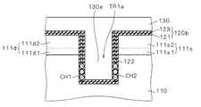
図60は、本実施の形態に係る半導体装置の備えるMONOSトランジスタを示す図である。図60に示すように、このMONOSトランジスタにおいては、溝TR1aはソース領域111sおよびドレイン領域111dよりも十分に深く形成され、ソース領域111sおよびドレイン領域111dは溝TR1aに隣接して形成されている。
【0176】
なお、ソース領域111sおよびドレイン領域111dのうち半導体基板110の内奥部側は、不純物濃度が比較的低いLDD領域111s1,111d1となっており、半導体基板110の表面側は、不純物濃度が比較的高い高濃度領域111s2,111d2となっている。
【0177】
そして、電荷CH1,CH2を保持することが可能な第1および第2の電荷保持部が、溝TR1aの側面のうちソース領域111sおよびドレイン領域111dよりも深い部分に隣接するゲート絶縁膜120内に形成されている。
【0178】
メモリセルとして、このMONOSトランジスタにプログラム動作およびイレース動作を行う場合は、実施の形態1の場合と同様にして、半導体基板110、ゲート電極130、ソース領域111sおよびドレイン領域111dの各部に適当な電圧を印加することにより行えばよい。
【0179】
なお、ソース領域111sおよびドレイン領域111dが溝TR1aに隣接して形成されているので、第1および第2の電荷保持部の位置は、図60に示すようにゲート絶縁膜120のうちソース領域111sおよびドレイン領域111dよりも深い部分になる。
【0180】
この場合も実施の形態1の場合と同様、第1の電荷保持部に電荷CH1をトラップさせた後に第2の電荷保持部に電荷CH2をトラップさせる場合に、ゲート電極のうち溝TR1a内の部分130eがシールドの役割を果たす。また、ソース領域111sおよびドレイン領域111d間に深い溝TR1aが形成されているので、実効チャネル長が大きくなり、パンチスルーへの耐性も向上する。
【0181】
本実施の形態の場合、溝TR1aの側面に隣接するゲート絶縁膜120内に第1および第2の電荷保持部を設けるので、ソース領域111sおよびドレイン領域111dを溝TR1aに隣接して形成することが可能であり、半導体基板110表面の平面視においてソース/ドレイン間の距離を小さくすることができる。
【0182】
すなわち、半導体基板110表面の平面視においてMONOSトランジスタのゲート長方向の長さを小さくすることができ、半導体基板110の表面に形成可能な素子数を増加させて集積度の向上が図れる。
【0183】
なお、図60の構造を形成するには、以下の方法を採用すればよい。すなわち、まず、不純物注入により半導体基板110の表面に不純物濃度が比較的低い低濃度領域を形成し、続いて、当該低濃度領域よりも浅く、不純物濃度が比較的高い高濃度領域を形成する。上記低濃度領域および高濃度領域には、必要に応じてアニール処理を行えばよい。
【0184】
次に、当該低濃度領域および高濃度領域を分断するように、溝TR1aをフォトリソグラフィ技術およびエッチング技術を用いて形成する。溝TR1aにより分断された両側の低濃度領域および高濃度領域は、ソース領域111sおよびドレイン領域111dとなる。
【0185】
次に、熱酸化法やCVD法等により半導体基板110上にシリコン酸化膜121を形成し、続いてCVD法等によりシリコン酸化膜121上にシリコン窒化膜122を形成する。そして、熱酸化法やCVD法等によりシリコン窒化膜122上にシリコン酸化膜123を形成し、ONO構造のゲート絶縁膜120を完成する。
【0186】
そして、シリコン酸化膜123上にゲート電極130を形成すれば、図60の構造が得られる。
【0187】
なお、図61は、本実施の形態に係る半導体装置の備えるMONOSトランジスタの他の例を示す図である。図61に示すように、このMONOSトランジスタにおいては、溝TR1aの側面部分においてのみシリコン酸化膜121、シリコン窒化膜122、シリコン酸化膜123のONO構造となっており、半導体基板110の表面上および溝TR1aの底面においてはシリコン窒化膜122が形成されない。それ以外の点は、図60の構造と同様である。
【0188】
この場合も、図60の半導体装置と同様に、第1の電荷保持部に電荷CH1をトラップさせた後に第2の電荷保持部に電荷CH2をトラップさせる場合に、ゲート電極のうち溝TR1a内の部分130eがシールドの役割を果たす。また、ソース領域111sおよびドレイン領域111d間に深い溝TR1aが形成されているので、実効チャネル長が大きくなり、パンチスルーへの耐性も向上する。そして、半導体基板110表面の平面視においてMONOSトランジスタのゲート長方向の長さを小さくすることができ、半導体基板110の表面に形成可能な素子数を増加させて集積度の向上が図れる。
【0189】
なお、図61の構造を形成するには、以下の方法を採用すればよい。すなわち、図60の構造を形成する場合と同様に、溝TR1a、ソース領域111s、ドレイン領域111d、シリコン酸化膜121およびシリコン窒化膜122を形成する。
【0190】
次に、シリコン窒化膜122に異方性エッチバックを施して、半導体基板110の表面上および溝TR1aの底面上のシリコン窒化膜122を除去する。これにより、シリコン窒化膜122は溝TR1aの側面にのみ残置する。
【0191】
その後、熱酸化法やCVD法等によりシリコン酸化膜121上およびシリコン窒化膜122上にシリコン酸化膜123を形成し、ゲート絶縁膜120bを完成する。そして、シリコン酸化膜123上にゲート電極130を形成すれば、図61の構造が得られる。
【0192】
【発明の効果】
請求項1に記載の発明によれば、MISトランジスタにおいて、ゲート電極が溝に入り込むようにゲート絶縁膜上に形成され、ゲート絶縁膜中には、第1および第2の電荷保持部が溝を挟むように形成されている。よって、第1の電荷保持部に電荷をトラップさせた後に第2の電荷保持部に電荷をトラップさせる場合に、溝内のゲート電極がシールドの役割を果たす。すなわち、第1の電荷保持部の電荷の誘起する電界の影響が第2の電荷保持部に及ぶことがなく、スケーリングが進んだ場合であっても第2の電荷保持部への電荷のトラップが妨げられることがない。よって、このMISトランジスタを不揮発性メモリのメモリセルに適用すれば、不揮発性メモリのスケーリングが進んだ場合にも、一つのメモリセルに多ビットの情報を保持させることが可能な半導体装置を実現できる。また、ソース領域およびドレイン領域間に溝が形成されているので実効チャネル長が大きくなり、パンチスルーへの耐性も向上する。さらに、ゲート絶縁膜のうち溝に入り込んだ部分には、第1および第2の電荷保持部は形成されない。よって、溝部分のゲート絶縁膜の膜厚を薄くすることができ、溝部分におけるチャネル生成に必要なゲート電圧の値を低く抑えることができる。
【0193】
請求項2に記載の発明によれば、ゲート絶縁膜は、第1のシリコン酸化膜、シリコン窒化膜、および、第2のシリコン酸化膜の順に積層された積層膜であって、第1および第2の電荷保持部とは、シリコン窒化膜のうち溝を挟む、互いに対向する第1および第2の部分である。よって、請求項1に係る半導体装置をMONOSトランジスタで実現できる。
【0195】
請求項3に記載の発明によれば、半導体基板上には、他のMISトランジスタも形成されている。よって、本発明に係る半導体装置を例えば、MISトランジスタをメモリセルに用い、他のMISトランジスタを論理回路の構成素子に用いるシステムLSI(Large Scale Integration)として構成することが可能である。
【0196】
請求項4に記載の発明によれば、ゲート絶縁膜のうち溝に入り込んだ部分には、第1および第2の電荷保持部は形成されず、かつ、他のMISトランジスタの他のゲート絶縁膜が延在して形成されている。よって、ゲート絶縁膜のうち溝に入り込んだ部分の材質を、他のゲート絶縁膜の材質と同じくすることができ、例えば高誘電率絶縁膜を溝部分に採用することが可能となる。
【0197】
請求項5に記載の発明によれば、第1および第2の電荷保持部は、ソース領域およびドレイン領域上に端部を有する。よって、請求項1に記載のMISトランジスタが連続して複数のメモリセルとして形成され、隣接するトランジスタ間でゲート絶縁膜を共有する場合であっても、メモリセルごとに第1および第2の電荷保持部が絶縁される。よって、メモリセル間で電荷の移動が生じることはない。
【0198】
請求項6に記載の発明によれば、第1および第2の電荷保持部の端部には、端部を覆う絶縁膜が形成されている。よって、ゲート電極が第1および第2の電荷保持部の終端部分にまで延在している場合であっても、第1および第2の電荷保持部に保持された電荷がゲート電極内に移動することを防止できる。
【0199】
請求項7に記載の発明によれば、溝の上端部および底部の角部分は丸められている。よって、角部分における電界の集中を抑制でき、半導体装置の信頼性を向上させることができる。
【0200】
請求項8に記載の発明によれば、第1および第2の電荷保持部は、ゲート絶縁膜内に複数形成された島状領域たるドットである。よって、第1および第2の電荷保持部がゲート絶縁膜内で連続する膜である場合に比べて、保持した電荷の移動がより起こりにくく、より不揮発性に優れた半導体装置を実現できる。
【0201】
請求項9に記載の発明によれば、島状領域たるドットは、シリコンまたはシリコン窒化膜で構成される。ゲート絶縁膜に例えばシリコン酸化膜を用いる場合、シリコンまたはシリコン窒化膜のドットにおけるエネルギー準位はシリコン酸化膜のエネルギー準位よりも安定している。よって、保持した電荷の移動が起こりにくく、不揮発性に優れた半導体装置を実現できる。
【図面の簡単な説明】
【図1】 実施の形態1に係る半導体装置を示す図である。
【図2】 実施の形態2に係る半導体装置の製造方法を示す図である。
【図3】 実施の形態2に係る半導体装置の製造方法を示す図である。
【図4】 実施の形態2に係る半導体装置の製造方法を示す図である。
【図5】 実施の形態3に係る半導体装置の製造方法を示す図である。
【図6】 実施の形態3に係る半導体装置の製造方法を示す図である。
【図7】 実施の形態3に係る半導体装置の製造方法を示す図である。
【図8】 実施の形態3に係る半導体装置の製造方法を示す図である。
【図9】 実施の形態3に係る半導体装置の製造方法を示す図である。
【図10】 実施の形態3に係る半導体装置の製造方法を示す図である。
【図11】 実施の形態3に係る半導体装置の製造方法を示す図である。
【図12】 実施の形態3に係る半導体装置の製造方法を示す図である。
【図13】 実施の形態3に係る半導体装置の製造方法を示す図である。
【図14】 実施の形態3に係る半導体装置の製造方法を示す図である。
【図15】 実施の形態4に係る半導体装置を示す図である。
【図16】 実施の形態4に係る半導体装置の他の例を示す図である。
【図17】 実施の形態5に係る半導体装置の製造方法を示す図である。
【図18】 実施の形態5に係る半導体装置の製造方法を示す図である。
【図19】 実施の形態5に係る半導体装置の製造方法を示す図である。
【図20】 実施の形態5に係る半導体装置の製造方法を示す図である。
【図21】 実施の形態6に係る半導体装置の製造方法を示す図である。
【図22】 実施の形態6に係る半導体装置の製造方法を示す図である。
【図23】 実施の形態6に係る半導体装置の製造方法を示す図である。
【図24】 実施の形態6に係る半導体装置の製造方法を示す図である。
【図25】 実施の形態6に係る半導体装置の製造方法を示す図である。
【図26】 実施の形態6に係る半導体装置の製造方法を示す図である。
【図27】 実施の形態7に係る半導体装置の製造方法を示す図である。
【図28】 実施の形態8に係る半導体装置を示す図である。
【図29】 実施の形態8に係る半導体装置の他の例を示す図である。
【図30】 実施の形態9に係る半導体装置の製造方法を示す図である。
【図31】 実施の形態10に係る半導体装置を示す図である。
【図32】 実施の形態11に係る半導体装置の製造方法を示す図である。
【図33】 実施の形態11に係る半導体装置の製造方法を示す図である。
【図34】 実施の形態12に係る半導体装置を示す図である。
【図35】 不揮発性メモリのメモリセルに利用される従来の半導体装置を示す断面図である。
【図36】 不揮発性メモリの構造を示す上面図である。
【図37】 不揮発性メモリのより具体的な構造の一例を示す斜視図である。
【図38】 不揮発性メモリのより具体的な構造の他の一例を示す斜視図である。
【図39】 従来の半導体装置のスケーリングを示す図である。
【図40】 従来の半導体装置において2ビットの情報を保持させる場合のスケーリングを示す図である。
【図41】 実施の形態14に係る半導体装置を示す図である。
【図42】 実施の形態14に係る半導体装置において情報を保持させる場合を示す図である。
【図43】 実施の形態14に係る半導体装置において情報を読み取る場合を示す図である。
【図44】 実施の形態14に係る半導体装置の他の例を示す図である。
【図45】 実施の形態14に係る半導体装置の他の例を示す図である。
【図46】 実施の形態15に係る半導体装置を示す図である。
【図47】 実施の形態15に係る半導体装置の他の例を示す図である。
【図48】 実施の形態15に係る半導体装置の他の例を示す図である。
【図49】 実施の形態16に係る半導体装置を示す図である。
【図50】 実施の形態17に係る半導体装置の製造方法を示す図である。
【図51】 実施の形態17に係る半導体装置の製造方法を示す図である。
【図52】 実施の形態17に係る半導体装置の製造方法を示す図である。
【図53】 実施の形態17に係る半導体装置の製造方法を示す図である。
【図54】 実施の形態18に係る半導体装置の製造方法を示す図である。
【図55】 実施の形態18に係る半導体装置の製造方法を示す図である。
【図56】 実施の形態18に係る半導体装置の製造方法を示す図である。
【図57】 実施の形態18に係る半導体装置の製造方法を示す図である。
【図58】 実施の形態19に係る半導体装置の製造方法を示す図である。
【図59】 実施の形態19に係る半導体装置の製造方法を示す図である。
【図60】 実施の形態20に係る半導体装置を示す図である。
【図61】 実施の形態20に係る半導体装置の他の例を示す図である。
【符号の説明】
110 半導体基板、111s ソース領域、111d ドレイン領域、120,120a,124,125,220,250 ゲート絶縁膜、121,123,127,129,129g,129i シリコン酸化膜、122,128 シリコン窒化膜、130 ゲート電極、140 素子分離領域、150 層間絶縁膜、203 ダミー膜、204 第1のマスク膜、206 サイドウォール膜、207 SOG、DT ドット、CH1,CH2 電荷。[0001]
BACKGROUND OF THE INVENTION
The present invention relates to a semiconductor device used for a memory cell of a nonvolatile memory and a manufacturing method thereof.
[0002]
[Prior art]
One of semiconductor devices used for memory cells of a nonvolatile memory is a MONOS (Metal Oxide Nitride Oxide Semiconductor) transistor having a structure shown in FIG. The MONOS transistor includes a
[0003]
Among these, the gate
[0004]
When the charge CH1 is trapped, a change occurs in the threshold voltage of the MONOS transistor compared to when the charge CH1 is not trapped. Therefore, by detecting this change in threshold voltage, it is determined whether 1-bit information is stored in the memory cell.
[0005]
FIG. 36 is a top view of the
[0006]
37 and 38 are both perspective views showing an example of a more specific structure of the
[0007]
On the other hand, the
[0008]
Note that prior art document information relating to the invention of this application includes the following.
[0009]
[Patent Document 1]
US Pat. No. 5,768,192
[Patent Document 2]
JP 2002-26149 A
[Patent Document 3]
JP-A-5-75133
[Non-Patent Document 1]
I. Bloom et al., “NROM anew non-volatile memory technology: from
device to products '', (USA), Microelectronic Engineering 59 (20
01), pp.213-223
[Non-Patent Document 2]
B. Eitan et al., `` Can NROM, a 2-bit, Trapping Storage NVM Cell,
Give a Real Challenge to Floating Gate Cells? (USA), SSDM1999
[Non-Patent Document 3]
E. Lusky et al., “Electron Discharge Model of Locally-Trapped
Charge in Oxide-Nitride-Oxide (ONO) Gates for NROM Non-Volatile
Semiconductor Memory Devices '' (USA), SSDM2001
[Non-Patent Document 4]
T.Toyoshima et al., `` 0.1μm Level Contact Hole Pattern Forma-
tion with KrF Lithography by Resolution Enhancement Lithogra-
phy Assisted by Chemical Shrink (RELACS) ”IEDM1998, p.333
[Non-Patent Document 5]
J. De Blauwe et al., `` Si-Dot Non-Volatile Memory Device '' (USA),
Extended Abstracts of the 2001 International Conference on
Solid State Devices and Materials, Tokyo, 2001, pp. 518-519
[0010]
[Problems to be solved by the invention]
As shown in FIG. 39, the channel length of the MONOS transistor (which is the same as the MONOS transistor of FIG. 35, but further includes a sidewall insulating film 160), which is a memory cell of the
[0011]
In this MONOS transistor, it is possible not only to trap the charge CH1 only on the
[0012]
The upper MONOS transistor in FIG. 40 shows a case where charges are trapped on each side of the source / drain. Here, the charge CH1 trapped on the
[0013]
As shown in the lower side of FIG. 40, when trapping charges on both sides of the source / drain, the channel length is shortened by scaling. At this time, if the charge is to be trapped on each side of the source / drain, trapping of the charge CH2 may be hindered by the repulsive force of the electric field EF1 induced by the initially trapped charge CH1 (in FIG. 40). Charge CH2a). Therefore, with the conventional semiconductor device structure, it becomes difficult to hold multi-bit information in one memory cell when scaling progresses.
[0014]
SUMMARY OF THE INVENTION An object of the present invention is to provide a semiconductor device capable of holding multi-bit information in one memory cell even when scaling of a nonvolatile memory is advanced, and a manufacturing method thereof.
[0015]
[Means for Solving the Problems]
According to the first aspect of the present invention, a semiconductor substrate having a groove on a surface thereof, a source region formed in the semiconductor substrate so as to face the surface, and the source region are separated from each other through the groove.FormedA drain region formed facing the surface in the semiconductor substrate, and a gate formed so as to enter the trench on at least a portion of the surface sandwiched between the source region and the drain region An MIS (Metal Insulator Semiconductor) transistor including an insulating film and a gate electrode formed on the gate insulating film so as to enter the trench is provided, and charges are held in the gate insulating film.Configured asThe first and second charge holding portions are formed so as to sandwich the groove.The first and second charge holding portions are not formed in the portion of the gate insulating film that has entered the trench.It is a semiconductor device.
[0016]
A second aspect of the present invention is the semiconductor device according to the first aspect, wherein the gate insulating film is laminated in the order of a first silicon oxide film, a silicon nitride film, and a second silicon oxide film. The first and second charge holding portions are semiconductor devices that are first and second portions facing each other across the groove in the silicon nitride film.
[0018]
Claim3The semiconductor device according to
[0019]
Claim4The invention described in claim3The first and second charge holding portions are not formed in a portion of the gate insulating film that has entered the trench, and the other of the other MIS transistors This is a semiconductor device formed by extending a gate insulating film.
[0020]
Claim5The semiconductor device according to
[0021]
Claim6The invention described in claim5The semiconductor device according to
[0022]
Claim7The invention according to
[0023]
Claim8The semiconductor device according to
[0024]
Claim9The invention described in claim82. The semiconductor device according to
[0025]
Claim 10The semiconductor device according to
[0027]
DETAILED DESCRIPTION OF THE INVENTION
<
This embodiment is a semiconductor device including a MONOS transistor having a structure in which a groove is formed in a channel portion and a silicon nitride film in a gate insulating film is formed as a charge holding portion with the groove interposed therebetween.
[0028]
FIG. 1 is a diagram illustrating a MONOS transistor included in the semiconductor device according to the present embodiment. As shown in FIG. 1, the MONOS transistor includes a
[0029]
In the present embodiment, the trench TR1 is formed in the channel portion between the
[0030]
Thus, if the trench TR1 is formed near the center of the channel and the
[0031]
When the program operation and the erase operation are performed on the MONOS transistor, a fixed potential such as 0 [V] or 3 [V] is applied to the
[0032]
Therefore, if this MONOS transistor is applied to a memory cell of a nonvolatile memory, a semiconductor device capable of holding multi-bit information in one memory cell even when the scaling of the nonvolatile memory progresses can be realized. . Of course, if a plurality of MONOS transistors shown in FIG. 1 are formed on the
[0033]
When a program operation and an erase operation are performed on the MONOS transistor as a memory cell, an appropriate voltage is applied to each part of the
[0034]
Since the trench TR1 is formed between the
[0035]
<
The present embodiment is an example of a method for manufacturing a semiconductor device according to the first embodiment.
[0036]
First, as shown in FIG. 2, a
[0037]
Next, well formation, channel doping, and the like are performed. After that, as shown in FIG. 3, a
[0038]
Then, a
[0039]
That is, after the formation of the
[0040]
Note that the
[0041]
After that, if the
[0042]
In this way, the semiconductor device according to the first embodiment can be manufactured. Further, since the
[0043]
Note that in this embodiment, the case where the
[0044]
However, the LDD regions 111sa and 111da may be formed after the
[0045]
In that case, a mask such as a photoresist is formed on the
[0046]
Next, the size of the mask is shrunk (reduced) by a necessary amount by resist ashing or the like. Thereafter, impurity implantation is performed to form a relatively low concentration LDD region.
[0047]
In this way, the LDD regions 111sa and 111da can be formed after the
[0048]
As in the above case, another example of forming the
[0049]
That is, in this case, a mask such as a photoresist is formed on the
[0050]
Next, the size of the mask is enlarged (increased) by a necessary amount by the RELACS technique. Thereafter, impurity implantation is performed to form a relatively high concentration source region and drain region.
[0051]
In this way, the
[0052]
In the above, the case where a photoresist is used as a mask has been shown. However, a silicon oxide film, a silicon nitride film, a poly-silicon film, or the like can be used as long as the material can secure an etching selectivity with respect to the underlying material and the exposed material. Silicon or the like may be used for the mask.
[0053]
When these materials are used to form the LDD regions 111sa and 111da after the formation of the
[0054]
An appropriate mask material may be selected in consideration of the base material and the preceding and following processes.
[0055]
In this embodiment, as shown in FIG. 4, the
[0056]
That is, as is generally performed, a photoresist may be formed on the
[0057]
Further, it is not essential to form the trench TR1 first and form the
[0058]
However, if the trench TR1 is formed first and the
[0059]
<Embodiment 3>
The present embodiment is another example of the method for manufacturing the semiconductor device according to the first embodiment.
[0060]
First, a dummy film (for example, silicon oxide film) 203 is formed on the
[0061]
Next, a
[0062]
Subsequently, the
[0063]
Next, on the
[0064]
Then, etching is performed using the
[0065]
Subsequently, the
[0066]
As a result, the trench TR1 is formed in the
[0067]
According to the present embodiment, trench TR1 is formed using
[0068]
<
The present embodiment is a modification of the semiconductor device according to the first embodiment, and a MONOS having a structure in which a
[0069]
FIG. 15 is a diagram illustrating a MONOS transistor included in the semiconductor device according to the present embodiment. As shown in FIG. 15, in this MONOS transistor, the
[0070]
Thus, if the
[0071]
Further, as shown in FIG. 16, if another MIS transistor having a
[0072]
If another MIS transistor is formed on the
[0073]
Then, by forming the
[0074]
<Embodiment 5>
The present embodiment is an example of a method for manufacturing a semiconductor device according to the fourth embodiment.
[0075]
First, as shown in FIG. 17, prior to the formation of the trench TR <b> 1, a
[0076]
Then, the trench TR1 is formed on the surface of the
[0077]
Next, a new
[0078]
Thereafter, as shown in FIG. 20, a
[0079]
After that, if the
[0080]
In the case of manufacturing the structure having the
[0081]
In the case of manufacturing the MONOS transistor shown in FIG. 16, for example, after the step of FIG. 18, the
[0082]
Note that the formation of the LDD region and the source / drain may be any as described in the second embodiment.
[0083]
<Embodiment 6>
The present embodiment is another example of the method for manufacturing a semiconductor device according to the fourth embodiment. In the present embodiment, it is assumed that a structure having an
[0084]
First, a
[0085]
Next, the
[0086]
Subsequently, using the
[0087]
Next, the trench TR1 is formed on the surface of the
[0088]
Thereafter,
[0089]
In this way, as in the second embodiment, since
[0090]
Of course, as described in the second embodiment, the mask for forming the
[0091]
<
This embodiment is another example of the method for manufacturing a semiconductor device according to the fourth embodiment. The present embodiment is a manufacturing method in which the
[0092]
First, a
[0093]
Next, a
[0094]
Subsequently, the
[0095]
Next, on the
[0096]
Then, etching is performed using the
[0097]
Subsequently, using the etching selectivity, the
[0098]
According to the present embodiment, trench TR1 is formed using
[0099]
<Eighth embodiment>
The present embodiment is a modification of the semiconductor device according to the fourth embodiment. In the
[0100]
FIG. 28 is a diagram illustrating a MONOS transistor included in the semiconductor device according to the present embodiment. As shown in FIG. 28, in this MONOS transistor, the
[0101]
As described above, if the
[0102]
Although it is unlikely that the charges trapped in the
[0103]
As shown in FIG. 29, an insulating film (for example, a silicon oxide film) 126 covering the termination portion may be formed at the termination portion of the
[0104]
<Embodiment 9>
The present embodiment is an example of a method for manufacturing a semiconductor device according to the eighth embodiment.
[0105]
In the present embodiment, the steps shown in FIGS. 17 to 19 are performed in the same manner as in the semiconductor device manufacturing method according to the fifth embodiment. Thereafter, as shown in FIG. 30, a
[0106]
Thereafter, the impurity implantation IP1 is performed while leaving the
[0107]
Thereafter, by removing the
[0108]
In the case of manufacturing the MONOS transistor shown in FIG. 29, the
[0109]
Note that the formation of the LDD region and the source / drain may be any as described in the second embodiment.
[0110]
<Embodiment 10>
The present embodiment is a modification of the semiconductor device according to the first embodiment, and is a semiconductor device including a MONOS transistor having a structure in which the upper end portion and the bottom corner portion of the trench TR1 are rounded.
[0111]
FIG. 31 is a diagram showing a MONOS transistor included in the semiconductor device according to the present embodiment. As shown in FIG. 31, in this MONOS transistor, the corner portions CR1 and CR2 at the top and bottom of the trench TR1 are rounded. Other configurations are the same as those of the MONOS transistor shown in FIG.
[0112]
Thus, if the corner portions CR1 and CR2 at the top and bottom of the trench TR1 are rounded, the concentration of the electric field at the corner can be suppressed, and the reliability of the semiconductor device can be improved.
[0113]
<Embodiment 11>
The present embodiment is an example of a method for manufacturing a semiconductor device according to the tenth embodiment.
[0114]
In the present embodiment, the process shown in FIG. 2 is performed in the same manner as in the method for manufacturing the semiconductor device according to the second embodiment, so that the trench TR1 is formed in the
[0115]
Thereafter, the
[0116]
<Embodiment 12>
The present embodiment is also a modification of the semiconductor device according to the first embodiment, and a dot that is a plurality of island-shaped regions formed of silicon without adopting a stacked structure including a silicon nitride film as a gate insulating film. This shows a case where a gate insulating film having the above is employed.
[0117]
A technique for forming silicon dots in a silicon oxide film is described in Non-Patent Document 5, for example. In the present embodiment, a silicon oxide film including such silicon dots is used for the gate insulating film.
[0118]
FIG. 34 is a diagram showing a MIS transistor included in the semiconductor device according to the present embodiment. In FIG. 34, the structure is the same as that of the semiconductor device according to the first embodiment except that the
[0119]
In the first embodiment, the charges CH1 and CH2 are held in the trap level in the
[0120]
In the case of the silicon dot DT, since it has conductivity, the trap level is deeper than that of the silicon nitride film and is stable regardless of the location. In other words, compared to the case where the first and second charge holding portions are continuous in the
[0121]
A technique for forming a silicon nitride film in the form of dots in a silicon oxide film instead of silicon dots is described in, for example, Patent Document 3 (see FIG. 1 of the publication). Even if it is a silicon nitride film, if it is a dot shape, compared with the case where it is a film | membrane continuous in the
[0122]
<Embodiment 13>
In the twelfth embodiment, the structure in which the
[0123]
In other words, if the structure of the MIS transistor is a structure in which a charge holding portion capable of holding charges, such as an ONO film or a dot, is formed in the gate insulating film of the present invention.
[0124]
<Embodiment 14>
This embodiment is a semiconductor device including a MONOS transistor having a structure in which a silicon nitride film in a gate insulating film is used as a charge holding portion and a gate insulating film on a channel central portion is only a lower silicon oxide film.
[0125]
FIG. 41 is a diagram showing a MONOS transistor included in the semiconductor device according to the present embodiment. As shown in FIG. 41, this MONOS transistor includes a
[0126]
Among these, the
[0127]
In the present embodiment, the first and second
[0128]
Then, on the center of the channel, that is, in the portion of the
[0129]
FIG. 42 is a diagram showing a case where information is held in the semiconductor device according to the present embodiment. FIG. 43 is a diagram showing a case where information is read in the semiconductor device according to the present embodiment.
[0130]
In FIG. 42, a ground potential 0 [V] (shown as “0”) is applied to the
[0131]
The portion where the first and second
[0132]
Further, only the extending portion 127a of the
[0133]
By applying a voltage to each part, charges (for example, electrons) CH2 move as channel hot electrons from the
[0134]
On the other hand, in FIG. 43, the ground potential 0 [V] (indicated as “0”) is applied to the
[0135]
Depending on the amount of charge CH2 trapped in the second
[0136]
In the case of performing the erase operation, an appropriate voltage may be applied to each part of the
[0137]
42, the charge CH1 is not shown in the first
[0138]
As described above, the channel CNb is formed deep in the center of the channel. Thereby, a large number of channel hot carriers (channel hot electrons in the case of electrons) can be generated. By generating a large number of channel hot carriers, the trap probability can be increased even when the second
[0139]
In addition, since the
[0140]
That is, in this embodiment as described above, the trap probability is high, and the
[0141]
41, the lengths L1 and L3 in the channel length direction of the first and second
[0142]
Note that the first and second
[0143]
In the
[0144]
The charges CH1 and CH2 to be trapped are not limited to electrons but may be holes, for example.
[0145]
Further, instead of the structure of FIG. 41, a structure as shown in FIG. 44 or 45 may be adopted. In both figures, the first and second
[0146]
Therefore, similar to the semiconductor device according to the eighth embodiment, even when the MONOS transistor according to the present embodiment is continuously formed as a plurality of memory cells and a gate insulating film is shared between adjacent transistors, The first and second
[0147]
<Embodiment 15>
The present embodiment is a modification of the semiconductor device according to the fourteenth embodiment, and is interposed between end portions of the first and second
[0148]
FIG. 46 shows a semiconductor device according to the present embodiment. In this semiconductor device, as shown in FIG. 46, the
[0149]
As described above, if the portion of the first and second
[0150]
47 and FIG. 48 are obtained by applying a
[0151]
As described above, if the source / drain side ends of the first and second
[0152]
<Embodiment 16>
This embodiment is also a modification of the semiconductor device according to the fourteenth embodiment, and the first and second charge holding portions of the gate insulating film are made of silicon without using a stacked structure including a silicon nitride film. An insulating film having dots formed as a plurality of island-shaped regions is employed.
[0153]
FIG. 49 is a diagram showing a MIS transistor included in the semiconductor device according to the present embodiment. In FIG. 49, an insulating film (for example, silicon oxide film) 250 including silicon dots DT is formed on the
[0154]
A
[0155]
Therefore, the thickness of the gate insulating film on the center of the channel, that is, the portion of the gate insulating film sandwiched between the insulating
[0156]
The structure is the same as that of the semiconductor device according to the fourteenth embodiment except that the gate insulating film is replaced with the insulating
[0157]
As described above, if the first and second charge holding portions are constituted by a plurality of dots formed in the gate insulating film, the first and second charge holding portions are gate insulating films like the
[0158]
Further, when, for example, a silicon oxide film is used as the gate insulating film, the energy level in the dots of the silicon or silicon nitride film is more stable than the energy level of the silicon oxide film. Therefore, if the dots are made of silicon or a silicon nitride film, the movement of the held charges hardly occurs, and a semiconductor device having excellent non-volatility can be realized.
[0159]
<Embodiment 17>
The present embodiment is an example of a method for manufacturing a semiconductor device according to the fourteenth embodiment.
[0160]
First, well formation, channel doping, or the like is performed in the
[0161]
Then, after removing the
[0162]
Next, a
[0163]
44 or 45, the shape of the
[0164]
In the above, the case where a photoresist is used as a mask has been shown. However, a silicon oxide film, a silicon nitride film, a poly-silicon film, or the like can be used as long as the material can secure an etching selectivity with respect to the underlying material and the exposed material. Silicon or the like may be used for the mask.
[0165]
<Embodiment 18>
The present embodiment is an example of a method for manufacturing a semiconductor device according to the fifteenth embodiment.
[0166]
First, in the same manner as in the seventeenth embodiment, the
[0167]
In addition to this, the structure of the semiconductor device according to the fifteenth embodiment may be manufactured as follows, for example. That is, as shown in FIG. 55, etching is performed up to the lower
[0168]
Alternatively, as shown in FIG. 57, after forming the
[0169]
<Embodiment 19>
The present embodiment is an example of a method for manufacturing a semiconductor device according to the sixteenth embodiment.
[0170]
First, as in FIG. 50, a
[0171]
Next, as shown in FIG. 58, a
[0172]
Thereafter, a conductive film such as polysilicon is formed on the
[0173]
In the case where a dot-like silicon nitride film is employed instead of silicon dots, for example, the technique described in Patent Document 3 may be used.
[0174]
<Embodiment 20>
The present embodiment is a modification of the semiconductor device according to the first embodiment, and is a semiconductor device in which the first and second charge holding portions are formed in the gate insulating film adjacent to the side surface of the trench. .
[0175]
FIG. 60 is a diagram showing a MONOS transistor included in the semiconductor device according to the present embodiment. As shown in FIG. 60, in this MONOS transistor, trench TR1a is formed sufficiently deeper than
[0176]
Of the
[0177]
The first and second charge holding portions capable of holding the charges CH1 and CH2 are formed in the
[0178]
When a program operation and an erase operation are performed on the MONOS transistor as a memory cell, appropriate voltages are applied to each part of the
[0179]
Since the
[0180]
Also in this case, as in the case of the first embodiment, when the charge CH1 is trapped in the first charge holding portion and then the charge CH2 is trapped in the second charge holding portion, the portion of the gate electrode in the
[0181]
In the present embodiment, since the first and second charge holding portions are provided in the
[0182]
That is, the length of the MONOS transistor in the gate length direction can be reduced in plan view of the surface of the
[0183]
In order to form the structure of FIG. 60, the following method may be employed. That is, first, a low concentration region having a relatively low impurity concentration is formed on the surface of the
[0184]
Next, the trench TR1a is formed using a photolithography technique and an etching technique so as to divide the low concentration region and the high concentration region. The low concentration region and the high concentration region on both sides divided by the trench TR1a become the
[0185]
Next, a
[0186]
If the
[0187]
FIG. 61 is a diagram showing another example of the MONOS transistor included in the semiconductor device according to the present embodiment. As shown in FIG. 61, this MONOS transistor has an ONO structure of a
[0188]
Also in this case, as in the semiconductor device of FIG. 60, when the charge CH1 is trapped in the second charge holding portion after the charge CH1 is trapped in the first charge holding portion, the gate electrode includes the trench TR1a in the trench TR1a. The
[0189]
In order to form the structure of FIG. 61, the following method may be employed. That is, as in the case of forming the structure of FIG. 60, the trench TR1a, the
[0190]
Next, anisotropic etching back is performed on the
[0191]
Thereafter, a
[0192]
【The invention's effect】
According to the first aspect of the present invention, in the MIS transistor, the gate electrode is formed on the gate insulating film so as to enter the groove, and in the gate insulating film, the first and second charge holding portions have the groove. It is formed so as to sandwich it. Therefore, when trapping charges in the second charge holding portion after trapping charges in the first charge holding portion, the gate electrode in the groove serves as a shield. That is, the influence of the electric field induced by the charge in the first charge holding portion does not reach the second charge holding portion, and even when scaling progresses, trapping of charges in the second charge holding portion is not caused. There is no hindrance. Therefore, when this MIS transistor is applied to a memory cell of a nonvolatile memory, a semiconductor device capable of holding multi-bit information in one memory cell even when the scaling of the nonvolatile memory progresses can be realized. . Further, since the groove is formed between the source region and the drain region, the effective channel length is increased, and the resistance to punch-through is improved.Further, the first and second charge holding portions are not formed in the portion of the gate insulating film that has entered the trench. Therefore, the thickness of the gate insulating film in the trench can be reduced, and the value of the gate voltage necessary for channel generation in the trench can be kept low.
[0193]
According to the second aspect of the present invention, the gate insulating film is a laminated film in which the first silicon oxide film, the silicon nitride film, and the second silicon oxide film are laminated in this order. The two charge holding portions are a first portion and a second portion facing each other across the groove in the silicon nitride film. Therefore, the semiconductor device according to
[0195]
Claim3According to the invention described in the above, another MIS transistor is also formed on the semiconductor substrate. Therefore, the semiconductor device according to the present invention can be configured as, for example, a system LSI (Large Scale Integration) that uses a MIS transistor as a memory cell and another MIS transistor as a component of a logic circuit.
[0196]
Claim4According to the invention, the first and second charge holding portions are not formed in the portion of the gate insulating film that has entered the trench, and the other gate insulating film of the other MIS transistor extends. Is formed. Therefore, the material of the portion of the gate insulating film that enters the groove can be made the same as the material of the other gate insulating film, and for example, a high dielectric constant insulating film can be adopted for the groove portion.
[0197]
Claim5According to the invention described in (1), the first and second charge holding portions have ends on the source region and the drain region. Therefore, even when the MIS transistor according to
[0198]
Claim6According to the invention, the insulating film that covers the end portions is formed at the end portions of the first and second charge holding portions. Therefore, even if the gate electrode extends to the terminal portions of the first and second charge holding portions, the charges held in the first and second charge holding portions move into the gate electrode. Can be prevented.
[0199]
Claim7According to the invention described in (1), the corners of the upper end and the bottom of the groove are rounded. Therefore, concentration of the electric field in the corner portion can be suppressed, and the reliability of the semiconductor device can be improved.
[0200]
Claim8According to the invention described in (1), the first and second charge holding portions are dots that are island-shaped regions formed in the gate insulating film. Therefore, compared with the case where the first and second charge holding portions are continuous films in the gate insulating film, the movement of the held charges is less likely to occur, and a semiconductor device that is more nonvolatile can be realized.
[0201]
Claim9According to the invention described in (1), the dots that are the island-shaped regions are made of silicon or a silicon nitride film. When, for example, a silicon oxide film is used as the gate insulating film, the energy level in the dots of the silicon or silicon nitride film is more stable than the energy level of the silicon oxide film. Therefore, the movement of the held charges hardly occurs, and a semiconductor device having excellent non-volatility can be realized.
[Brief description of the drawings]
FIG. 1 is a diagram illustrating a semiconductor device according to a first embodiment.
FIG. 2 is a diagram showing a method for manufacturing a semiconductor device according to a second embodiment.
FIG. 3 is a diagram showing a method for manufacturing a semiconductor device according to a second embodiment.
FIG. 4 is a diagram illustrating a method for manufacturing the semiconductor device according to the second embodiment.
FIG. 5 is a diagram illustrating the method for manufacturing the semiconductor device according to the third embodiment.
6 is a diagram illustrating a method for manufacturing the semiconductor device according to the third embodiment; FIG.
7 is a diagram illustrating the method of manufacturing the semiconductor device according to the third embodiment. FIG.
FIG. 8 is a diagram illustrating the method of manufacturing the semiconductor device according to the third embodiment.
FIG. 9 is a diagram illustrating the method of manufacturing the semiconductor device according to the third embodiment.
FIG. 10 is a diagram illustrating the method of manufacturing the semiconductor device according to the third embodiment.
FIG. 11 is a diagram illustrating the method of manufacturing the semiconductor device according to the third embodiment.
FIG. 12 is a diagram illustrating the method of manufacturing the semiconductor device according to the third embodiment.
FIG. 13 is a diagram illustrating the method of manufacturing the semiconductor device according to the third embodiment.
FIG. 14 is a diagram illustrating the method of manufacturing the semiconductor device according to the third embodiment.
FIG. 15 shows a semiconductor device according to the fourth embodiment.
FIG. 16 is a diagram illustrating another example of the semiconductor device according to the fourth embodiment.
FIG. 17 is a diagram illustrating the method of manufacturing the semiconductor device according to the fifth embodiment.
FIG. 18 is a diagram illustrating the method of manufacturing the semiconductor device according to the fifth embodiment.
FIG. 19 is a diagram illustrating the method of manufacturing the semiconductor device according to the fifth embodiment.
FIG. 20 is a diagram illustrating the method of manufacturing the semiconductor device according to the fifth embodiment.
FIG. 21 is a diagram illustrating the method of manufacturing the semiconductor device according to the sixth embodiment.
FIG. 22 is a diagram illustrating the method of manufacturing the semiconductor device according to the sixth embodiment.
FIG. 23 is a diagram illustrating the method of manufacturing the semiconductor device according to the sixth embodiment.
FIG. 24 is a diagram illustrating the manufacturing method of the semiconductor device according to the sixth embodiment.
FIG. 25 is a diagram illustrating the manufacturing method of the semiconductor device according to the sixth embodiment.
FIG. 26 is a diagram illustrating the method of manufacturing the semiconductor device according to the sixth embodiment.
FIG. 27 is a diagram illustrating the manufacturing method of the semiconductor device according to the seventh embodiment.
FIG. 28 shows a semiconductor device according to the eighth embodiment.
FIG. 29 is a diagram showing another example of a semiconductor device according to the eighth embodiment.
30 is a diagram illustrating the method of manufacturing the semiconductor device according to the ninth embodiment. FIG.
FIG. 31 is a diagram showing a semiconductor device according to a tenth embodiment;
FIG. 32 is a diagram illustrating the manufacturing method of the semiconductor device according to the eleventh embodiment;
FIG. 33 is a diagram illustrating the manufacturing method of the semiconductor device according to the eleventh embodiment;
34 shows a semiconductor device according to the twelfth embodiment; FIG.
FIG. 35 is a cross-sectional view showing a conventional semiconductor device used for a memory cell of a nonvolatile memory.
FIG. 36 is a top view illustrating a structure of a nonvolatile memory.
FIG. 37 is a perspective view showing an example of a more specific structure of a nonvolatile memory.
FIG. 38 is a perspective view showing another example of a more specific structure of the nonvolatile memory.
FIG. 39 is a diagram illustrating scaling of a conventional semiconductor device.
FIG. 40 is a diagram illustrating scaling when 2 bits of information is held in a conventional semiconductor device.
41 shows a semiconductor device according to the fourteenth embodiment; FIG.
42 is a diagram showing a case where information is held in a semiconductor device according to Embodiment 14; FIG.
43 is a diagram showing a case where information is read in the semiconductor device according to the fourteenth embodiment; FIG.
44 is a diagram showing another example of a semiconductor device according to Embodiment 14; FIG.
45 is a diagram showing another example of a semiconductor device according to Embodiment 14; FIG.
FIG. 46 shows a semiconductor device according to the fifteenth embodiment;
47 is a diagram showing another example of the semiconductor device according to the fifteenth embodiment; FIG.
48 is a diagram showing another example of the semiconductor device according to the fifteenth embodiment; FIG.
49 shows a semiconductor device according to the sixteenth embodiment; FIG.
FIG. 50 is a diagram illustrating the method of manufacturing the semiconductor device according to Embodiment 17;
FIG. 51 is a diagram illustrating the manufacturing method of the semiconductor device according to the seventeenth embodiment;
FIG. 52 is a diagram illustrating the method of manufacturing the semiconductor device according to Embodiment 17;
FIG. 53 is a diagram illustrating the method of manufacturing the semiconductor device according to Embodiment 17;
FIG. 54 shows a method for manufacturing the semiconductor device according to the eighteenth embodiment;
FIG. 55 shows a method for manufacturing the semiconductor device according to the eighteenth embodiment;
FIG. 56 shows a method for manufacturing the semiconductor device according to the eighteenth embodiment;
FIG. 57 shows a method for manufacturing the semiconductor device according to the eighteenth embodiment;
FIG. 58 shows a method for manufacturing the semiconductor device according to the nineteenth embodiment;
FIG. 59 shows a method for manufacturing the semiconductor device according to the nineteenth embodiment;
60 is a diagram showing a semiconductor device according to a twentieth embodiment; FIG.
61 is a diagram showing another example of a semiconductor device according to Embodiment 20. FIG.
[Explanation of symbols]
110 semiconductor substrate, 111s source region, 111d drain region, 120, 120a, 124, 125, 220, 250 gate insulating film, 121, 123, 127, 129, 129g, 129i silicon oxide film, 122, 128 silicon nitride film, 130 Gate electrode, 140 element isolation region, 150 interlayer insulating film, 203 dummy film, 204 first mask film, 206 sidewall film, 207 SOG, DT dot, CH1, CH2 charge.
Claims (10)
Translated fromJapanese前記半導体基板内において前記表面に面して形成されたソース領域、前記ソース領域とは前記溝を介して離隔して形成され、前記半導体基板内において前記表面に面して形成されたドレイン領域、前記表面のうち少なくとも前記ソース領域と前記ドレイン領域とに挟まれた部分の上に、前記溝に入り込むように形成されたゲート絶縁膜、および、前記ゲート絶縁膜上に、前記溝に入り込むように形成されたゲート電極を含むMIS(Metal Insulator Semiconductor)トランジスタと
を備え、
前記ゲート絶縁膜中には、電荷を保持するように構成された第1および第2の電荷保持部が前記溝を挟むように形成されており、
前記ゲート絶縁膜のうち前記溝に入り込んだ部分には、前記第1および第2の電荷保持部は形成されない
半導体装置。A semiconductor substrate having a groove on the surface;
A source region formed facing the surface in the semiconductor substrate, a drain regionformed separately from the source region via the groove, and formed facing the surface in the semiconductor substrate, A gate insulating film formed so as to enter the trench on at least a portion of the surface sandwiched between the source region and the drain region, and so as to enter the trench on the gate insulating film. MIS (Metal Insulator Semiconductor) transistor including the formed gate electrode,
In the gate insulating film, first and second charge holding portionsconfigured to hold charges are formed so as to sandwich the groove,
The first and second charge holding portions are not formed in a portion of the gate insulating film that has entered the trench . A semiconductor device.
前記ゲート絶縁膜は、第1のシリコン酸化膜、シリコン窒化膜、および、第2のシリコン酸化膜の順に積層された積層膜であって、
前記第1および第2の電荷保持部とは、前記シリコン窒化膜のうち前記溝を挟む、互いに対向する第1および第2の部分である
半導体装置。The semiconductor device according to claim 1,
The gate insulating film is a stacked film in which a first silicon oxide film, a silicon nitride film, and a second silicon oxide film are stacked in this order,
The first and second charge holding portions are semiconductor devices that are first and second portions facing each other across the groove in the silicon nitride film.
前記半導体基板上には、他のソース領域、他のドレイン領域、他のゲート絶縁膜および他のゲート電極を有する他のMISトランジスタも形成されている
半導体装置。The semiconductor device according to claim 1,
Another MIS transistor having another source region, another drain region, another gate insulating film, and another gate electrode is also formed on the semiconductor substrate .
前記ゲート絶縁膜のうち前記溝に入り込んだ部分には、前記第1および第2の電荷保持部は形成されず、かつ、前記他のMISトランジスタの前記他のゲート絶縁膜が延在して形成されている
半導体装置。The semiconductor device according to claim3 ,
The first and second charge holding portions are not formed in a portion of the gate insulating film that has entered the trench, and the other gate insulating film of the other MIS transistor is formed to extend. Semiconductor device.
前記第1および第2の電荷保持部は、前記ソース領域および前記ドレイン領域上に端部を有する
半導体装置。The semiconductor device according to claim1 ,
It saidfirst and second charge carrier holding portion is a semiconductor device thathaving a end portion to said source region and said drain region.
前記第1および第2の電荷保持部の前記端部には、前記端部を覆う絶縁膜が形成された
半導体装置。The semiconductor device according to claim5 ,
The semiconductor device, wherein an insulating film that covers the end portions is formed at the end portions of the first and second charge holding portions.
前記溝の上端部および底部の角部分は丸められている
半導体装置。The semiconductor device according to claim1 ,
A semiconductor device, whereincorners of an upper end portion and a bottom portion of the groove are rounded .
前記第1および第2の電荷保持部は、前記ゲート絶縁膜内に複数形成された島状領域である
半導体装置。The semiconductor device according to claim 1,
Saidfirst and second charge carrier holding portion, said gate insulating film island region der Ru semiconductor devicehaving a plurality formed in the.
前記島状領域は、シリコンまたはシリコン窒化膜で構成される
半導体装置。The semiconductor device according to claim8 ,
Theisland region is a semiconductor device thatconsists of silicon or silicon nitride film.
前記第1および第2の電荷保持部は、前記溝の側面に隣接する前記ゲート絶縁膜内に形成された
半導体装置。The semiconductor device according to claim1 ,
The semiconductor device, whereinthe first and second charge holding portions are formed in the gate insulating film adjacent to a side surface of the trench .
Priority Applications (6)
| Application Number | Priority Date | Filing Date | Title |
|---|---|---|---|
| JP2003009516AJP4412903B2 (en) | 2002-06-24 | 2003-01-17 | Semiconductor device |
| TW092116950ATWI223453B (en) | 2002-06-24 | 2003-06-23 | Semiconductor device |
| US10/600,344US6867455B2 (en) | 2002-06-24 | 2003-06-23 | Semiconductor device with a metal insulator semiconductor transistor |
| CNB031487521ACN1293645C (en) | 2002-06-24 | 2003-06-24 | Semiconductor device |
| US11/052,142US20050169050A1 (en) | 2002-06-24 | 2005-02-08 | Semiconductor device with a metal insulator semiconductor transistor |
| US11/690,704US20070190724A1 (en) | 2002-06-24 | 2007-03-23 | Semiconductor device |
Applications Claiming Priority (2)
| Application Number | Priority Date | Filing Date | Title |
|---|---|---|---|
| JP2002182441 | 2002-06-24 | ||
| JP2003009516AJP4412903B2 (en) | 2002-06-24 | 2003-01-17 | Semiconductor device |
Publications (2)
| Publication Number | Publication Date |
|---|---|
| JP2004088055A JP2004088055A (en) | 2004-03-18 |
| JP4412903B2true JP4412903B2 (en) | 2010-02-10 |
Family
ID=31497574
Family Applications (1)
| Application Number | Title | Priority Date | Filing Date |
|---|---|---|---|
| JP2003009516AExpired - Fee RelatedJP4412903B2 (en) | 2002-06-24 | 2003-01-17 | Semiconductor device |
Country Status (4)
| Country | Link |
|---|---|
| US (3) | US6867455B2 (en) |
| JP (1) | JP4412903B2 (en) |
| CN (1) | CN1293645C (en) |
| TW (1) | TWI223453B (en) |
Families Citing this family (23)
| Publication number | Priority date | Publication date | Assignee | Title |
|---|---|---|---|---|
| JP2004179387A (en)* | 2002-11-27 | 2004-06-24 | Renesas Technology Corp | Nonvolatile semiconductor memory device and method of manufacturing the same |
| US20060192249A1 (en)* | 2004-09-20 | 2006-08-31 | Samsung Electronics Co., Ltd. | Field effect transistors with vertically oriented gate electrodes and methods for fabricating the same |
| JP4334315B2 (en) | 2003-10-10 | 2009-09-30 | 株式会社ルネサステクノロジ | Manufacturing method of semiconductor memory device |
| US7348625B2 (en)* | 2004-08-11 | 2008-03-25 | Macronix International Co., Ltd. | Semiconductor device and method of manufacturing the same |
| KR100598106B1 (en)* | 2004-08-27 | 2006-07-07 | 삼성전자주식회사 | Sonos memory cell and its formation method |
| KR100674948B1 (en) | 2005-01-20 | 2007-01-26 | 삼성전자주식회사 | Multi-bit nonvolatile memory device and manufacturing method |
| US7365382B2 (en)* | 2005-02-28 | 2008-04-29 | Infineon Technologies Ag | Semiconductor memory having charge trapping memory cells and fabrication method thereof |
| KR100643542B1 (en) | 2005-03-16 | 2006-11-10 | 삼성전자주식회사 | Non-volatile memory device having a charge trap layer and method of manufacturing same |
| KR100752661B1 (en)* | 2005-04-09 | 2007-08-29 | 삼성전자주식회사 | Field effect transistors with vertically oriented gate electrodes and method of fabricating the same |
| KR100704033B1 (en) | 2005-08-05 | 2007-04-04 | 삼성전자주식회사 | Charge-Trap 3-Level Nonvolatile Semiconductor Memory Device and Driving Method Therefor |
| US7292478B2 (en)* | 2005-09-08 | 2007-11-06 | Macronix International Co., Ltd. | Non-volatile memory including charge-trapping layer, and operation and fabrication of the same |
| JP2008010739A (en)* | 2006-06-30 | 2008-01-17 | Toshiba Corp | Semiconductor device and manufacturing method thereof |
| JP2008053270A (en)* | 2006-08-22 | 2008-03-06 | Nec Electronics Corp | Semiconductor memory device and manufacturing method thereof |
| WO2008072692A1 (en) | 2006-12-15 | 2008-06-19 | Nec Corporation | Nonvolatile storage device and method for manufacturing the same |
| JP2008166528A (en) | 2006-12-28 | 2008-07-17 | Spansion Llc | Semiconductor device and manufacturing method thereof |
| US7480184B2 (en) | 2007-01-07 | 2009-01-20 | International Business Machines Corporation | Maximum likelihood statistical method of operations for multi-bit semiconductor memory |
| KR100869745B1 (en)* | 2007-06-01 | 2008-11-21 | 주식회사 동부하이텍 | Semiconductor device and manufacturing method thereof |
| JP2009277782A (en)* | 2008-05-13 | 2009-11-26 | Oki Semiconductor Co Ltd | Semiconductor memory and its production process |
| US7936009B2 (en)* | 2008-07-09 | 2011-05-03 | Fairchild Semiconductor Corporation | Shielded gate trench FET with an inter-electrode dielectric having a low-k dielectric therein |
| IT1396561B1 (en)* | 2009-03-13 | 2012-12-14 | St Microelectronics Srl | METHOD FOR REALIZING A POWER DEVICE WITH A TRENCH-GATE STRUCTURE AND ITS DEVICE |
| JP5110153B2 (en)* | 2010-11-08 | 2012-12-26 | 住友電気工業株式会社 | Semiconductor device and manufacturing method thereof |
| US9947701B2 (en) | 2016-05-31 | 2018-04-17 | Taiwan Semiconductor Manufacturing Company, Ltd. | Low noise device and method of forming the same |
| KR102555788B1 (en)* | 2018-04-30 | 2023-07-17 | 삼성디스플레이 주식회사 | Thin film transistor substrate, method of manufacturing the same, and display device including the same |
Family Cites Families (22)
| Publication number | Priority date | Publication date | Assignee | Title |
|---|---|---|---|---|
| US4693781A (en)* | 1986-06-26 | 1987-09-15 | Motorola, Inc. | Trench formation process |
| JPH0575133A (en) | 1991-09-11 | 1993-03-26 | Rohm Co Ltd | Non-volatile storage device |
| TW326553B (en)* | 1996-01-22 | 1998-02-11 | Handotai Energy Kenkyusho Kk | Semiconductor device and method of fabricating same |
| US5768192A (en) | 1996-07-23 | 1998-06-16 | Saifun Semiconductors, Ltd. | Non-volatile semiconductor memory cell utilizing asymmetrical charge trapping |
| US5793090A (en)* | 1997-01-10 | 1998-08-11 | Advanced Micro Devices, Inc. | Integrated circuit having multiple LDD and/or source/drain implant steps to enhance circuit performance |
| US6281545B1 (en)* | 1997-11-20 | 2001-08-28 | Taiwan Semiconductor Manufacturing Company | Multi-level, split-gate, flash memory cell |
| KR100278285B1 (en)* | 1998-02-28 | 2001-01-15 | 김영환 | Cmos image sensor and method for fabricating the same |
| KR100291179B1 (en)* | 1998-06-29 | 2001-07-12 | 박종섭 | Cmos image sensor having a self-aligned silicide layer and method for fabricating the same |
| JP2000260887A (en) | 1999-03-08 | 2000-09-22 | Nec Corp | Nonvolatile semiconductor memory device and its manufacture |
| US6630712B2 (en)* | 1999-08-11 | 2003-10-07 | Advanced Micro Devices, Inc. | Transistor with dynamic source/drain extensions |
| JP4834897B2 (en) | 2000-05-02 | 2011-12-14 | ソニー株式会社 | Nonvolatile semiconductor memory device and operation method thereof |
| US6512274B1 (en)* | 2000-06-22 | 2003-01-28 | Progressant Technologies, Inc. | CMOS-process compatible, tunable NDR (negative differential resistance) device and method of operating same |
| JP3688980B2 (en)* | 2000-06-28 | 2005-08-31 | 株式会社東芝 | MOS type solid-state imaging device and manufacturing method thereof |
| JP4923321B2 (en)* | 2000-09-12 | 2012-04-25 | ソニー株式会社 | Method of operating nonvolatile semiconductor memory device |
| JP3984020B2 (en)* | 2000-10-30 | 2007-09-26 | 株式会社東芝 | Nonvolatile semiconductor memory device |
| US6897522B2 (en)* | 2001-10-31 | 2005-05-24 | Sandisk Corporation | Multi-state non-volatile integrated circuit memory systems that employ dielectric storage elements |
| US6486028B1 (en)* | 2001-11-20 | 2002-11-26 | Macronix International Co., Ltd. | Method of fabricating a nitride read-only-memory cell vertical structure |
| US20030134476A1 (en)* | 2002-01-17 | 2003-07-17 | Yakov Roizin | Oxide-nitride-oxide structure |
| KR100450670B1 (en)* | 2002-02-09 | 2004-10-01 | 삼성전자주식회사 | Image sensor having photo diode and method for manufacturing the same |
| US7042045B2 (en)* | 2002-06-04 | 2006-05-09 | Samsung Electronics Co., Ltd. | Non-volatile memory cell having a silicon-oxide nitride-oxide-silicon gate structure |
| US6706599B1 (en)* | 2003-03-20 | 2004-03-16 | Motorola, Inc. | Multi-bit non-volatile memory device and method therefor |
| US7214575B2 (en)* | 2004-01-06 | 2007-05-08 | Micron Technology, Inc. | Method and apparatus providing CMOS imager device pixel with transistor having lower threshold voltage than other imager device transistors |
- 2003
- 2003-01-17JPJP2003009516Apatent/JP4412903B2/ennot_activeExpired - Fee Related
- 2003-06-23TWTW092116950Apatent/TWI223453B/ennot_activeIP Right Cessation
- 2003-06-23USUS10/600,344patent/US6867455B2/ennot_activeExpired - Fee Related
- 2003-06-24CNCNB031487521Apatent/CN1293645C/ennot_activeExpired - Fee Related
- 2005
- 2005-02-08USUS11/052,142patent/US20050169050A1/ennot_activeAbandoned
- 2007
- 2007-03-23USUS11/690,704patent/US20070190724A1/ennot_activeAbandoned
Also Published As
| Publication number | Publication date |
|---|---|
| US6867455B2 (en) | 2005-03-15 |
| US20040026745A1 (en) | 2004-02-12 |
| US20050169050A1 (en) | 2005-08-04 |
| US20070190724A1 (en) | 2007-08-16 |
| TW200402884A (en) | 2004-02-16 |
| CN1503371A (en) | 2004-06-09 |
| JP2004088055A (en) | 2004-03-18 |
| CN1293645C (en) | 2007-01-03 |
| TWI223453B (en) | 2004-11-01 |
Similar Documents
| Publication | Publication Date | Title |
|---|---|---|
| JP4412903B2 (en) | Semiconductor device | |
| KR100640620B1 (en) | NOR type flash memory device of twin bit cell structure and manufacturing method thereof | |
| US7309634B2 (en) | Non-volatile semiconductor memory devices using prominences and trenches | |
| JP4659527B2 (en) | Manufacturing method of semiconductor device | |
| US6744097B2 (en) | EEPROM memory cell and method of forming the same | |
| KR101038873B1 (en) | Manufacturing Method of Flash Memory Device | |
| US20090173992A1 (en) | Semiconductor device with improved performance characteristics | |
| US6686243B2 (en) | Fabrication method for flash memory | |
| US20170062446A1 (en) | Semiconductor device and method of manufacturing the same | |
| KR100568445B1 (en) | A method of manufacturing a partial sonos type gate structure and a method of manufacturing a nonvolatile memory cell having the same | |
| JP4445353B2 (en) | Manufacturing method of direct tunnel semiconductor memory device | |
| CN104051468A (en) | Backgate Non-Volatile Memory Cell | |
| JP4424886B2 (en) | Semiconductor memory device and manufacturing method thereof | |
| KR100348311B1 (en) | Nonvolatile Memory Device and method for Fabricating the same | |
| JP2004014978A (en) | Nonvolatile semiconductor memory device | |
| CN111430353B (en) | Nonvolatile memory and manufacturing method thereof | |
| JP2022055951A (en) | Method for manufacturing semiconductor device | |
| JP4427431B2 (en) | Semiconductor memory device, semiconductor memory device manufacturing method, and semiconductor memory device operating method | |
| JP5014591B2 (en) | Semiconductor device and manufacturing method thereof | |
| KR20060062554A (en) | Nonvolatile Memory Device with Uneven Structure Active Area and Manufacturing Method Thereof | |
| KR100642383B1 (en) | Flash memory device having improved erase efficiency and manufacturing method thereof | |
| CN102891184B (en) | Non-volatile memory and its manufacturing method | |
| US8288815B2 (en) | Gate structure of semiconductor device having a conductive structure with a middle portion and two spacer portions | |
| JP2008192803A (en) | Semiconductor device and manufacturing method thereof | |
| US7163862B1 (en) | Semiconductor memory devices and methods for fabricating the same |
Legal Events
| Date | Code | Title | Description |
|---|---|---|---|
| A621 | Written request for application examination | Free format text:JAPANESE INTERMEDIATE CODE: A621 Effective date:20051108 | |
| A977 | Report on retrieval | Free format text:JAPANESE INTERMEDIATE CODE: A971007 Effective date:20090316 | |
| A131 | Notification of reasons for refusal | Free format text:JAPANESE INTERMEDIATE CODE: A131 Effective date:20090901 | |
| A521 | Request for written amendment filed | Free format text:JAPANESE INTERMEDIATE CODE: A523 Effective date:20091020 | |
| RD04 | Notification of resignation of power of attorney | Free format text:JAPANESE INTERMEDIATE CODE: A7424 Effective date:20091020 | |
| TRDD | Decision of grant or rejection written | ||
| A01 | Written decision to grant a patent or to grant a registration (utility model) | Free format text:JAPANESE INTERMEDIATE CODE: A01 Effective date:20091117 | |
| A01 | Written decision to grant a patent or to grant a registration (utility model) | Free format text:JAPANESE INTERMEDIATE CODE: A01 | |
| A61 | First payment of annual fees (during grant procedure) | Free format text:JAPANESE INTERMEDIATE CODE: A61 Effective date:20091117 | |
| FPAY | Renewal fee payment (event date is renewal date of database) | Free format text:PAYMENT UNTIL: 20121127 Year of fee payment:3 | |
| R150 | Certificate of patent or registration of utility model | Free format text:JAPANESE INTERMEDIATE CODE: R150 | |
| FPAY | Renewal fee payment (event date is renewal date of database) | Free format text:PAYMENT UNTIL: 20121127 Year of fee payment:3 | |
| S111 | Request for change of ownership or part of ownership | Free format text:JAPANESE INTERMEDIATE CODE: R313111 | |
| FPAY | Renewal fee payment (event date is renewal date of database) | Free format text:PAYMENT UNTIL: 20121127 Year of fee payment:3 | |
| R350 | Written notification of registration of transfer | Free format text:JAPANESE INTERMEDIATE CODE: R350 | |
| FPAY | Renewal fee payment (event date is renewal date of database) | Free format text:PAYMENT UNTIL: 20121127 Year of fee payment:3 | |
| FPAY | Renewal fee payment (event date is renewal date of database) | Free format text:PAYMENT UNTIL: 20131127 Year of fee payment:4 | |
| S531 | Written request for registration of change of domicile | Free format text:JAPANESE INTERMEDIATE CODE: R313531 | |
| R350 | Written notification of registration of transfer | Free format text:JAPANESE INTERMEDIATE CODE: R350 | |
| LAPS | Cancellation because of no payment of annual fees |