JP4408313B2 - Plasma processing apparatus and plasma processing method - Google Patents
Plasma processing apparatus and plasma processing methodDownload PDFInfo
- Publication number
- JP4408313B2 JP4408313B2JP30876599AJP30876599AJP4408313B2JP 4408313 B2JP4408313 B2JP 4408313B2JP 30876599 AJP30876599 AJP 30876599AJP 30876599 AJP30876599 AJP 30876599AJP 4408313 B2JP4408313 B2JP 4408313B2
- Authority
- JP
- Japan
- Prior art keywords
- frequency power
- electrode
- high frequency
- plasma
- frequency
- Prior art date
- Legal status (The legal status is an assumption and is not a legal conclusion. Google has not performed a legal analysis and makes no representation as to the accuracy of the status listed.)
- Expired - Fee Related
Links
- 238000003672processing methodMethods0.000titleclaimsdescription9
- 238000005530etchingMethods0.000description16
- 238000000034methodMethods0.000description12
- 230000008569processEffects0.000description9
- 238000001020plasma etchingMethods0.000description6
- 239000011162core materialSubstances0.000description4
- 229910004298SiO 2Inorganic materials0.000description3
- 239000004065semiconductorSubstances0.000description3
- 238000007796conventional methodMethods0.000description2
- 238000004519manufacturing processMethods0.000description2
- 238000012986modificationMethods0.000description2
- 230000004048modificationEffects0.000description2
- 238000009832plasma treatmentMethods0.000description2
- 230000009471actionEffects0.000description1
- 230000002411adverseEffects0.000description1
- 230000008859changeEffects0.000description1
- 239000004020conductorSubstances0.000description1
- 239000000470constituentSubstances0.000description1
- 230000007423decreaseEffects0.000description1
- 230000000694effectsEffects0.000description1
- NBVXSUQYWXRMNV-UHFFFAOYSA-NfluoromethaneChemical compoundFCNBVXSUQYWXRMNV-UHFFFAOYSA-N0.000description1
- 230000010354integrationEffects0.000description1
- 239000000463materialSubstances0.000description1
- 208000024891symptomDiseases0.000description1
Images
Classifications
- H—ELECTRICITY
- H01—ELECTRIC ELEMENTS
- H01J—ELECTRIC DISCHARGE TUBES OR DISCHARGE LAMPS
- H01J37/00—Discharge tubes with provision for introducing objects or material to be exposed to the discharge, e.g. for the purpose of examination or processing thereof
- H01J37/32—Gas-filled discharge tubes
- H01J37/32009—Arrangements for generation of plasma specially adapted for examination or treatment of objects, e.g. plasma sources
- H01J37/32082—Radio frequency generated discharge
- H01J37/32137—Radio frequency generated discharge controlling of the discharge by modulation of energy
- H01J37/32155—Frequency modulation
- H01J37/32165—Plural frequencies
Landscapes
- Physics & Mathematics (AREA)
- Engineering & Computer Science (AREA)
- Plasma & Fusion (AREA)
- Chemical & Material Sciences (AREA)
- Analytical Chemistry (AREA)
- Plasma Technology (AREA)
- ing And Chemical Polishing (AREA)
- Drying Of Semiconductors (AREA)
Description
Translated fromJapanese【0001】
【発明の属する技術分野】
本発明は,プラズマ処理装置およびプラズマ処理方法に関する。
【0002】
【従来の技術】
従来,半導体装置の製造工程においては,各種プラズマ処理,例えばプラズマエッチング処理が行われている。プラズマエッチング処理は,プラズマエッチング装置を用いて行われる。該装置としては,処理室内に上部電極と下部電極とを対向配置した平行平板型装置が広く使用されている。かかる装置では,上部電極への第1高周波電力の印加により,処理室内に導入された処理ガスがプラズマ化される。さらに,下部電極に第1高周波電力よりも低い周波数の第2高周波電力を印加することにより,プラズマが被処理体に引き込まれる。このため,下部電極上に載置された被処理体,例えば半導体ウェハ(以下,「ウェハ」と称する。)に所定のエッチング処理が施される。
【0003】
また,最近,半導体装置の超小型化および超高集積化傾向に伴い,エッチング処理においても超微細加工が要求されている。さらに,スループットの向上を図るために,処理の迅速化が求められている。このため,かかる技術的要求を達成するべく,プラズマエッチング装置の各種改良が試みられている。例えば,酸化膜(SiO2膜)用のエッチング装置では,プラズマ生成用の第1高周波電力の周波数を従来の13.56MHz程度の周波数よりも高い周波数,例えば60MHzに高めることにより,エッチングレートを向上させる技術が提案されている。ただし,かかる周波数の第1高周波電力を用いた場合には,プラズマの分布が不均一になり易くなる。そこで,さらに上記第2高周波電力をパワースプリッタにより電圧を分割し,分割された電力の一部を下部電極に印加し,一部を第1高周波電力に重畳する技術が提案されている。かかる重畳高周波電力によりプラズマを生成すると,プラズマの分布が均一化される。このため,高周波数の第1高周波電力を用いて処理を行っても,エッチングレートを向上させながら均一な処理を行うことが可能になる。さらに,ウェハの損傷も軽減される。このため,ウェハに超微細化処理を歩留り良く施すことが可能になる。
【0004】
【発明が解決しようとする課題】
最近,生産性を向上させる観点から,大口径のウェハに処理を施すことが求められている。このため,エッチング処理においては,容積が大きい処理室内にプラズマを均一に生成し,かつ大型のウェハ全面にプラズマを均一に導入する必要がある。その結果,ウェハの大口径化に伴い,より大パワー(電力量)の高周波電力を上部電極および下部電極に印加することが求められる。しかしながら,上記パワースプリッタは,一種のトランスなので,第2高周波電力のパワーが大きくなると構成部材である線材やコア材が大型化する。また,パワースプリッタは,電力の供給効率向上の観点から一般的に下部電極近傍に設けられる。その結果,エッチング装置が大型化し,フットプリントの削減が困難であるという問題点がある。
【0005】
また,コア材は,高周波電力のパワーや使用する周波数などに応じて製造されている。さらに,コア材は,適用される高周波電力のパワーが大きくなるほど特殊な構成になり,汎用性が低下する。このため,大パワー用のパワースプリッタを採用すると,装置の生産コストが増加するという問題点がある。
【0006】
また,上記従来の技術では,パワースプリッタにより第2高周波電力を分割している。パワースプリッタでは,上部電極および下部電極に印加する電圧を所定の電圧比に設定することができる。しかし,処理時には,生成されたプラズマの作用により,上部電極から見たインピーダンスと下部電極から見たインピーダンスとの比が変化する。このため,パワースプリッタを用いた場合には,上記インピーダンス比の変化により,上部電極および下部電極に各々印加される分割された第2高周波電力のパワーが変化する。その結果,上記分割された第2高周波電力のパワーの制御が困難になり,より一層の処理の均一化を図ることができないという問題点がある。
【0007】
本発明は,従来の技術が有する上記問題点に鑑みて成されたものである。そして,本発明の目的は,上記問題点およびその他の問題点を解決することが可能な,新規かつ改良されたプラズマ処理装置およびプラズマ処理方法を提供することである。
【0008】
【課題を解決するための手段】
上記課題を解決するために,本発明の第1の観点によれば,請求項1に記載の発明のように,処理室内に対向配置された第1電極と第2電極との各々に高周波電力を印加して処理室内にプラズマを生成し,第2電極上に載置された被処理体にプラズマ処理を施すプラズマ処理装置において,第1電極に第1高周波電力を印加する第1高周波電源と,第2電極に第1高周波電力よりも低い周波数の第2高周波電力を印加する第2高周波電源と,第1高周波電力の周波数よりも低く第2高周波電力の周波数よりも高い周波数の第3高周波電力を出力し,第1高周波電力に第3高周波電力を重畳する第3高周波電源と,第2高周波電源と第3高周波電源に接続され,第2高周波電力の位相と第3高周波電力の位相との位相差を調整する位相制御手段と,を備えることを特徴とする,プラズマ処理装置が提供される。
【0009】
かかる構成によれば,第1高周波電力に重畳する第3高周波電力を,第2高周波電源とは個別独立した第3高周波電源から出力する。かかる構成によれば,パワースプリッタを設けずに,重畳高周波電力を第1電極に印加できる。その結果,イニシャルコストの低下および装置の小型化を図ることができる。また,第2高周波電力と第3高周波電力の位相や周波数やパワーを,それぞれプロセスに応じて容易に変更できる。その結果,被処理体の膜質や大きさ等に応じたプラズマの制御が可能になり,被処理体に均一な処理を施すことができる。
【0010】
さらに,前記第3高周波電源は、前記第1電極に前記第1高周波電力が印加された後、前記第1電極に前記第3高周波電力を印加し、前記第2高周波電源は、前記第1電極に前記第3高周波電力が印加された後、前記第2電極に前記第2高周波電力を印加することが好ましい。
【0011】
また,本発明の第2の観点によれば,処理室内に対向配置された第1電極と第2電極とを備え,第1電極に第1高周波電力を印加し,第2電極に第1高周波電力よりも低い周波数の第2高周波電力を印加して処理室内にプラズマを生成し,第2電極上に載置された被処理体にプラズマ処理を施すプラズマ処理方法であって,第1電極に第1高周波電力を印加する第1工程と,第1工程の後に,第1電極に第1高周波電力の周波数よりも低く第2高周波電力の周波数以上の周波数の第3高周波電力を印加し,第1高周波電力と第3高周波電力とを重畳させる第2工程と,第2工程の後に,第2電極に第2高周波電力を印加する第3工程とを含み,さらに第2高周波電力の位相と第3高周波電力の位相との位相差を調整する第4工程を含むことを特徴とする,プラズマ処理方法が提供される。
【0012】
かかる構成によれば,第1電極に第1高周波電力と第3高周波電力とを順次印加した後に,第2電極に第2高周波電力が印加される。さらに,第2高周波電力と第3高周波電力の位相差が調整される。このため,プラズマの着火,プラズマの安定生成,被処理体へのプラズマの均一な導入を容易かつ確実に行うことができる。
【0013】
【発明の実施の形態】
以下に,添付図面を参照しながら本発明にかかるプラズマ処理装置およびプラズマ処理方法を,プラズマエッチング装置およびプラズマエッチング方法に適用した好適な実施の一形態について,詳細に説明する。
【0014】
(1)エッチング装置の構成
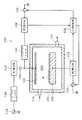
まず,図1を参照しながら,本発明を適用可能なエッチング装置100について概説する。エッチング装置100の処理室102は,導電性の気密な処理容器104内に形成されている。処理容器104は,保安接地されている。また,処理室102内には,上部電極(第1電極)106と下部電極(第2電極)108とが対向配置されている。上部電極106と下部電極108は,それぞれ導電性材料から形成されている。また,下部電極108は,ウェハWの載置台を兼ねている。また,上部電極106と下部電極108には,それぞれ後述する電力供給系が接続されている。また,処理室102内には,処理ガスがガス供給経路110を介して導入される。また,処理室102内のガスは,排気経路112を介して排気される。
【0015】
(2)電力供給系の構成
次に,上部電極106および下部電極108への基本的な電力供給構成について説明する。上部電極106には,第1高周波電源114がローパス(低域通過)フィルタ116,第1整合器118,キャパシタンス120を介して接続されている。かかる構成により,上部電極106には,所定周波数,例えば60MHzで5kWの第1高周波電力を印加できる。ただし,キャパシタンス120は,第1高周波電力を選択的に通過させるとともに,後述する第3高周波電力の第1整合器118への進入を防止する。また,下部電極108には,第2高周波電源122が第2整合器124を介して接続されている。かかる構成により,下部電極108には,第1高周波電力の周波数よりも低い周波数,例えば2MHzで5kWの第2高周波電力を印加できる。なお,上記各構成は,キャパシタンス120が設けられていることを除き,従来の装置と同様である。
【0016】
次に,本発明の中核をなす電力供給系について説明する。上部電極106には,上述した第1高周波電源114に加え,本実施の形態の特徴である第3高周波電源126が第3整合器128,バンドパス(帯域通過)フィルタ130を介して接続されている。かかる構成により,上部電極106には,第1高周波電力の周波数よりも低く第2高周波電力の周波数以上の周波数,あるいは第2高周波電力の周波数と同一の周波数の第3高周波電力と,上述した第1高周波電力との重畳高周波電力を印加できる。なお,本実施の形態では,第3高周波電力は,例えば第2高周波電力の周波数と同一の2MHzで2kWに設定されている。また,第3高周波電源126は,上部電極106とキャパシタンス120との間に接続されている。このため,上述したように,第3高周波電力が第1整合器118に進入せず,第1整合器118の整合動作に悪影響を及ぼすことがない。また,バンドパスフィルタ130は,上記2MHzの第3高周波電力を選択的に通過させるとともに,第1高周波電力の第3整合器128への進入を防止するフィルタである。このため,第1高周波電力が第3整合器128に進入せず,第3整合器118の整合動作の動作不良が生じることがない。
【0017】
また,第2高周波電源122と第3高周波電源126には,位相制御器132が接続されている。位相制御器132は,第2整合器124での第2高周波電力の位相と,第3整合器128での第3高周波電力の位相とを検出する。さらに,位相制御器132は,検出された第2高周波電力の位相と第3高周波電力の位相とに基づいて,第2高周波電源122と第3高周波電源126を制御する。かかる制御により,第2高周波電力の位相と第3高周波電力の位相に所定の位相差を生じさせることができる。その結果,プラズマの状態やプロセスに応じてプラズマを制御でき,ウェハWに均一な処理を施すことができる。
【0018】
(3)エッチング処理
次に,上述したエッチング装置100を用いたエッチング処理について説明する。まず,下部電極108上にウェハWを載置する。ウェハWの被処理面には,SiO2膜が形成されている。次いで,処理室102内に処理ガス,例えばフルオロカーボン系ガスを導入する。同時に,処理室102内を真空引きし,所定の減圧雰囲気に維持する。
【0019】
上記諸条件が整った後,まず第1高周波電源114から出力される60MHzの第1高周波電力を上部電極106に印加する。かかる電力の印加により,処理ガスがプラズマ化する。ただし,第1高周波電力の印加だけでは,すでに説明したように,第1高周波電力の周波数が高いために,生成されるプラズマの分布が不均一になり易い。そこで,第1高周波電力の印加後,第3高周波電源126から出力される2MHzの第3高周波電力を上部電極106に印加する。かかる電力の印加により,上部電極106には,第1高周波電力と第3高周波電力とが重畳された高周波電力が印加される。その結果,上記プラズマの分布が均一化される。さらに,第3高周波電力の印加後,第2高周波電源122から出力される2MHzの第2高周波電力を下部電極108に印加する。かかる電力の印加により,プラズマがウェハWに均一に導入される。その結果,ウェハWのSiO2膜に,高エッチングレートで均一な処理を施すことができ,所定形状のコンタクトホールを形成できる。また,ウェハWにプラズマを均一に導入できるので,プラズマの偏りに伴うウェハWの損傷を防止できる。
【0020】
また,上記構成によれば,第2高周波電源122と第3高周波電源126とが個別独立に設けられている。このため,パワースプリッタを使用せずに第2高周波電力および第3高周波電力を供給できる。その結果,装置構成を簡素化でき,かつイニシャルコストも減少させることができる。また,第2高周波電力と第3高周波電力とを独立して制御できる。その結果,高周波電力の制御性が向上し,処理をより均一に行うことができる。さらに,プロセスマージンも拡大できる。
【0021】
以上,本発明の好適な実施の一形態について,添付図面を参照しながら説明したが,本発明はかかる構成に限定されるものではない。特許請求の範囲に記載された技術的思想の範疇において,当業者であれば,各種の変更例および修正例に想到し得るものであり,それら変更例および修正例についても本発明の技術的範囲に属するものと了解される。
【0022】
【発明の効果】
本発明によれば,プラズマ生成用の第1高周波電力に重畳する第3高周波電力とバイアス用の第2高周波電力の位相,周波数,パワーを個別独立かつ容易に変えることができる。その結果,プラズマの制御を容易かつ的確に行うことができる。
【図面の簡単な説明】
【図1】本発明を適用可能なエッチング装置を示す概略的な断面図である。
【符号の説明】
100 エッチング装置
102 処理室
106 上部電極
108 下部電極
114 第1高周波電源
122 第2高周波電源
126 第3高周波電源
132 位相制御器
W ウェハ[0001]
BACKGROUND OF THE INVENTION
The present invention relates to a plasma processing apparatus and a plasma processing method.
[0002]
[Prior art]
Conventionally, various plasma processing, for example, plasma etching processing is performed in the manufacturing process of a semiconductor device. The plasma etching process is performed using a plasma etching apparatus. As the apparatus, a parallel plate type apparatus in which an upper electrode and a lower electrode are arranged to face each other in a processing chamber is widely used. In such an apparatus, the processing gas introduced into the processing chamber is turned into plasma by the application of the first high-frequency power to the upper electrode. Furthermore, the plasma is drawn into the object by applying a second high frequency power having a frequency lower than the first high frequency power to the lower electrode. Therefore, a predetermined etching process is performed on an object to be processed placed on the lower electrode, for example, a semiconductor wafer (hereinafter referred to as “wafer”).
[0003]
Recently, with the trend toward ultra-miniaturization and ultra-high integration of semiconductor devices, ultra-fine processing is also required for etching processing. Furthermore, in order to improve throughput, speeding up of processing is required. For this reason, various improvements of the plasma etching apparatus have been attempted in order to achieve such technical requirements. For example, in an etching apparatus for an oxide film (SiO2 film), the etching rate is improved by increasing the frequency of the first high-frequency power for plasma generation to a frequency higher than the conventional frequency of about 13.56 MHz, for example, 60 MHz. Techniques to make it have been proposed. However, when the first high frequency power having such a frequency is used, the plasma distribution tends to be non-uniform. Therefore, a technique has been proposed in which the voltage of the second high-frequency power is further divided by a power splitter, a part of the divided power is applied to the lower electrode, and a part is superimposed on the first high-frequency power. When plasma is generated by such superposed high-frequency power, the plasma distribution is made uniform. Therefore, even when processing is performed using the first high-frequency power having a high frequency, it is possible to perform uniform processing while improving the etching rate. In addition, wafer damage is reduced. For this reason, it is possible to perform ultra-fine processing on the wafer with a high yield.
[0004]
[Problems to be solved by the invention]
Recently, from the viewpoint of improving productivity, it is required to process a large-diameter wafer. For this reason, in the etching process, it is necessary to uniformly generate plasma in a processing chamber having a large volume and to introduce the plasma uniformly over the entire surface of a large wafer. As a result, as the wafer diameter increases, it is required to apply higher power (electric power) of high frequency power to the upper electrode and the lower electrode. However, since the power splitter is a kind of transformer, when the power of the second high-frequency power is increased, the wire material and the core material which are constituent members are enlarged. The power splitter is generally provided near the lower electrode from the viewpoint of improving the power supply efficiency. As a result, there is a problem that the etching apparatus becomes large and it is difficult to reduce the footprint.
[0005]
The core material is manufactured according to the power of the high frequency power, the frequency to be used, and the like. Furthermore, the core material has a special configuration as the power of the applied high-frequency power increases, and the versatility decreases. For this reason, if a power splitter for high power is used, there is a problem that the production cost of the apparatus increases.
[0006]
In the above conventional technique, the second high-frequency power is divided by the power splitter. In the power splitter, the voltage applied to the upper electrode and the lower electrode can be set to a predetermined voltage ratio. However, during processing, the ratio of the impedance seen from the upper electrode to the impedance seen from the lower electrode changes due to the action of the generated plasma. For this reason, when the power splitter is used, the power of the divided second high-frequency power applied to the upper electrode and the lower electrode changes due to the change in the impedance ratio. As a result, there is a problem that it becomes difficult to control the power of the divided second high-frequency power, and further uniform processing cannot be achieved.
[0007]
The present invention has been made in view of the above-described problems of conventional techniques. An object of the present invention is to provide a new and improved plasma processing apparatus and plasma processing method capable of solving the above problems and other problems.
[0008]
[Means for Solving the Problems]
In order to solve the above-described problems, according to a first aspect of the present invention, as in the first aspect of the present invention, high-frequency power is applied to each of the first electrode and the second electrode that are opposed to each other in the processing chamber. A first high frequency power source for applying a first high frequency power to the first electrode in a plasma processing apparatus for generating plasma in the processing chamber and applying a plasma treatment to an object to be processed placed on the second electrode; the second high frequency power source and the third high frequency having a frequencyhigher than the frequency of the second high frequency power lower than the frequency of the first high-frequency power applied to the second high-frequency power having a frequency lower than the first high-frequency power to the second electrode A third high-frequency power source for outputting power and superimposing the third high-frequency power on the first high-frequency power; and a second high-frequency power source and a third high-frequency power source connected to the second high-frequency power phase and the third high-frequency power phase; Control means for adjusting the phase difference of , Characterized in that it comprises a plasma processing apparatus is provided.
[0009]
According to such a configuration, the third high-frequency power superimposed on the first high-frequency power is output from the third high-frequency power supply that is independent from the second high-frequency power supply. According to such a configuration, it is possible to apply superimposed high frequency power to the first electrode without providing a power splitter. As a result, the initial cost can be reduced and the apparatus can be downsized. Further, the phase, frequency, and power of the second high-frequency power and the third high-frequency power can be easily changed according to the process. As a result, the plasma can be controlled according to the film quality and size of the object to be processed, and the object to be processed can be uniformly processed.
[0010]
Further,the third high frequency power supply applies the third high frequency power to the first electrode after the first high frequency power is applied to the first electrode, and the second high frequency power supply includes the first electrode. after the third high-frequency power is applied to the child applies the second high-frequency power to the second electrode is preferable.
[0011]
According to the second aspect of the presentinvention, a first electrode and a second electrode disposed opposite to theprocessing chamber, the first high-frequency power is applied to the first electrode, the first to the second electrode A plasma processing method for generating a plasma in a processing chamber by applying a second high-frequency power having a frequency lower than the high-frequency power, and performing a plasma treatment on an object to be processed placed on a second electrode. Applying a first high-frequency power to the first electrode, and applying a third high-frequency power having a frequency lower than the frequency of the first high-frequency power and higher than the frequency of the second high-frequency power to the first electrode after the first step; A second step of superimposing the first high-frequency power and the third high-frequency power; a third step of applying the second high-frequency power to the second electrode after the second step; Including a fourth step of adjusting a phase difference with the phase of the third high-frequency power. The symptom, the plasma processing method is provided.
[0012]
According to this configuration, the first high frequency power and the third high frequency power are sequentially applied to the first electrode, and then the second high frequency power is applied to the second electrode. Further, the phase difference between the second high frequency power and the third high frequency power is adjusted. For this reason, it is possible to easily and reliably perform plasma ignition, stable plasma generation, and uniform introduction of plasma into the workpiece.
[0013]
DETAILED DESCRIPTION OF THE INVENTION
Hereinafter, a preferred embodiment in which a plasma processing apparatus and a plasma processing method according to the present invention are applied to a plasma etching apparatus and a plasma etching method will be described in detail with reference to the accompanying drawings.
[0014]
(1) Configuration of Etching Apparatus First, an
[0015]
(2) Configuration of Power Supply System Next, a basic power supply configuration to the
[0016]
Next, the power supply system that forms the core of the present invention will be described. In addition to the first high
[0017]
A
[0018]
(3) Etching Process Next, an etching process using the above-described
[0019]
After the above conditions are satisfied, first, a 60 MHz first high frequency power output from the first high
[0020]
Further, according to the above configuration, the second high
[0021]
The preferred embodiment of the present invention has been described above with reference to the accompanying drawings, but the present invention is not limited to such a configuration. Within the scope of the technical idea described in the claims, those skilled in the art will be able to conceive of various changes and modifications, and these changes and modifications are also within the technical scope of the present invention. It is understood that it belongs to.
[0022]
【The invention's effect】
According to the present invention, the phase, frequency, and power of the third high-frequency power superimposed on the first high-frequency power for plasma generation and the second high-frequency power for bias can be changed independently and easily. As a result, plasma can be controlled easily and accurately.
[Brief description of the drawings]
FIG. 1 is a schematic cross-sectional view showing an etching apparatus to which the present invention can be applied.
[Explanation of symbols]
DESCRIPTION OF
Claims (4)
Translated fromJapanese前記第1電極に第1高周波電力を印加する第1高周波電源と;
前記第2電極に前記第1高周波電力よりも低い周波数の第2高周波電力を印加する第2高周波電源と;
前記第1高周波電力の周波数よりも低く前記第2高周波電力の周波数よりも高い周波数の第3高周波電力を出力し,前記第1高周波電力に前記第3高周波電力を重畳する第3高周波電源と;
前記第2高周波電源と前記第3高周波電源に接続され,前記第2高周波電力の位相と前記第3高周波電力の位相との位相差を調整する位相制御手段と;
を備えることを特徴とする,プラズマ処理装置。A high-frequency power is applied to each of the first electrode and the second electrode that are arranged opposite to each other in the processing chamber to generate plasma in the processing chamber, and plasma processing is performed on the object to be processed placed on the second electrode. In the plasma processing equipment to be applied:
A first high frequency power supply for applying a first high frequency power to the first electrode;
A second high frequency power supply for applying a second high frequency power having a frequency lower than the first high frequency power to the second electrode;
And outputting a third high-frequency power having a frequencyhigher than the frequency of the second RF power lower than the frequency of the first high frequency power, and a third high-frequency power source for superimposing the third high-frequency power to the first high-frequency power;
Phase control means connected to the second high-frequency power source and the third high-frequency power source to adjust a phase difference between the phase of the second high-frequency power and the phase of the third high-frequency power;
A plasma processing apparatus comprising:
前記第2高周波電源は、前記第1電極に前記第3高周波電力が印加された後、前記第2電極に前記第2高周波電力を印加する請求項1に記載のプラズマ処理装置。 2. The plasma processing apparatus according to claim 1, wherein the second high frequency power supply applies the second high frequency power to the second electrode after the third high frequency power is applied to the first electrode.
前記第1電極に前記第1高周波電力を印加する第1工程と;
前記第1工程の後に,前記第1電極に前記第1高周波電力の周波数よりも低く前記第2高周波電力の周波数以上の周波数の第3高周波電力を印加し,前記第1高周波電力と前記第3高周波電力とを重畳させる第2工程と;
前記第2工程の後に,前記第2電極に前記第2高周波電力を印加する第3工程と;を含み,
さらに,前記第2高周波電力の位相と前記第3高周波電力の位相との位相差を調整する第4工程を含むこと;
を特徴とする,プラズマ処理方法。A first electrode and a second electrode disposed opposite to each other in the processing chamber, wherein a first high frequency power is applied to the first electrode, and a second high frequency power having a frequency lower than the first high frequency power is applied to the second electrode. A plasma processing method of applying plasma to generate plasma in the processing chamber and performing plasma processing on an object to be processed placed on the second electrode:
Applying a first high-frequency power to the first electrode;
After the first step, third high frequency power having a frequency lower than the frequency of the first high frequency power and higher than the frequency of the second high frequency power is applied to the first electrode, and the first high frequency power and the third high frequency power are applied. A second step of superimposing high-frequency power;
After the second step, a third step of applying the second high-frequency power to the second electrode;
And a fourth step of adjusting a phase difference between the phase of the second high frequency power and the phase of the third high frequency power;
A plasma processing method characterized by
を特徴とする,請求項3に記載のプラズマ処理方法。 The plasma processing method according to claim 3, wherein:
Priority Applications (3)
| Application Number | Priority Date | Filing Date | Title |
|---|---|---|---|
| JP30876599AJP4408313B2 (en) | 1999-10-29 | 1999-10-29 | Plasma processing apparatus and plasma processing method |
| US10/361,772US6849154B2 (en) | 1998-11-27 | 2003-02-11 | Plasma etching apparatus |
| US11/028,239US20050115677A1 (en) | 1998-11-27 | 2005-01-04 | Plasma etching apparatus |
Applications Claiming Priority (1)
| Application Number | Priority Date | Filing Date | Title |
|---|---|---|---|
| JP30876599AJP4408313B2 (en) | 1999-10-29 | 1999-10-29 | Plasma processing apparatus and plasma processing method |
Publications (2)
| Publication Number | Publication Date |
|---|---|
| JP2001127045A JP2001127045A (en) | 2001-05-11 |
| JP4408313B2true JP4408313B2 (en) | 2010-02-03 |
Family
ID=17985038
Family Applications (1)
| Application Number | Title | Priority Date | Filing Date |
|---|---|---|---|
| JP30876599AExpired - Fee RelatedJP4408313B2 (en) | 1998-11-27 | 1999-10-29 | Plasma processing apparatus and plasma processing method |
Country Status (1)
| Country | Link |
|---|---|
| JP (1) | JP4408313B2 (en) |
Families Citing this family (38)
| Publication number | Priority date | Publication date | Assignee | Title |
|---|---|---|---|---|
| JP3776856B2 (en)* | 2002-09-13 | 2006-05-17 | 株式会社日立ハイテクノロジーズ | Plasma processing apparatus and plasma processing method |
| US20050069651A1 (en)* | 2003-09-30 | 2005-03-31 | Tokyo Electron Limited | Plasma processing system |
| US7169256B2 (en)* | 2004-05-28 | 2007-01-30 | Lam Research Corporation | Plasma processor with electrode responsive to multiple RF frequencies |
| KR101144018B1 (en)* | 2004-05-28 | 2012-05-09 | 램 리써치 코포레이션 | Plasma processor with electrode responsive to multiple rf frequencies |
| JP4773079B2 (en) | 2004-11-26 | 2011-09-14 | 株式会社日立ハイテクノロジーズ | Control method of plasma processing apparatus |
| CN100362619C (en)* | 2005-08-05 | 2008-01-16 | 中微半导体设备(上海)有限公司 | Radio Frequency Matching Coupling Network of Vacuum Reaction Chamber and Its Configuration Method |
| US20080029385A1 (en) | 2006-08-03 | 2008-02-07 | Tokyo Electron Limited | Plasma processing apparatus and plasma processing method |
| US8262847B2 (en)* | 2006-12-29 | 2012-09-11 | Lam Research Corporation | Plasma-enhanced substrate processing method and apparatus |
| US7547636B2 (en)* | 2007-02-05 | 2009-06-16 | Lam Research Corporation | Pulsed ultra-high aspect ratio dielectric etch |
| TWI531023B (en)* | 2009-11-19 | 2016-04-21 | 蘭姆研究公司 | Methods and apparatus for controlling a plasma processing system |
| US8901935B2 (en) | 2009-11-19 | 2014-12-02 | Lam Research Corporation | Methods and apparatus for detecting the confinement state of plasma in a plasma processing system |
| US8501631B2 (en) | 2009-11-19 | 2013-08-06 | Lam Research Corporation | Plasma processing system control based on RF voltage |
| US20110192349A1 (en)* | 2010-01-12 | 2011-08-11 | Hammond Iv Edward P | Phase-Modulated RF Power for Plasma Chamber Electrode |
| US9842725B2 (en) | 2013-01-31 | 2017-12-12 | Lam Research Corporation | Using modeling to determine ion energy associated with a plasma system |
| US9502216B2 (en) | 2013-01-31 | 2016-11-22 | Lam Research Corporation | Using modeling to determine wafer bias associated with a plasma system |
| US9320126B2 (en) | 2012-12-17 | 2016-04-19 | Lam Research Corporation | Determining a value of a variable on an RF transmission model |
| US9390893B2 (en) | 2012-02-22 | 2016-07-12 | Lam Research Corporation | Sub-pulsing during a state |
| US9197196B2 (en) | 2012-02-22 | 2015-11-24 | Lam Research Corporation | State-based adjustment of power and frequency |
| US9462672B2 (en) | 2012-02-22 | 2016-10-04 | Lam Research Corporation | Adjustment of power and frequency based on three or more states |
| US10325759B2 (en) | 2012-02-22 | 2019-06-18 | Lam Research Corporation | Multiple control modes |
| US9171699B2 (en) | 2012-02-22 | 2015-10-27 | Lam Research Corporation | Impedance-based adjustment of power and frequency |
| US9368329B2 (en) | 2012-02-22 | 2016-06-14 | Lam Research Corporation | Methods and apparatus for synchronizing RF pulses in a plasma processing system |
| US10128090B2 (en) | 2012-02-22 | 2018-11-13 | Lam Research Corporation | RF impedance model based fault detection |
| US9295148B2 (en) | 2012-12-14 | 2016-03-22 | Lam Research Corporation | Computation of statistics for statistical data decimation |
| US10157729B2 (en) | 2012-02-22 | 2018-12-18 | Lam Research Corporation | Soft pulsing |
| US9114666B2 (en) | 2012-02-22 | 2015-08-25 | Lam Research Corporation | Methods and apparatus for controlling plasma in a plasma processing system |
| US9408288B2 (en) | 2012-09-14 | 2016-08-02 | Lam Research Corporation | Edge ramping |
| US9779196B2 (en) | 2013-01-31 | 2017-10-03 | Lam Research Corporation | Segmenting a model within a plasma system |
| US9620337B2 (en) | 2013-01-31 | 2017-04-11 | Lam Research Corporation | Determining a malfunctioning device in a plasma system |
| US9107284B2 (en) | 2013-03-13 | 2015-08-11 | Lam Research Corporation | Chamber matching using voltage control mode |
| US9119283B2 (en) | 2013-03-14 | 2015-08-25 | Lam Research Corporation | Chamber matching for power control mode |
| TWI692798B (en)* | 2013-05-09 | 2020-05-01 | 美商蘭姆研究公司 | Segmenting a model within a plasma system |
| US9502221B2 (en) | 2013-07-26 | 2016-11-22 | Lam Research Corporation | Etch rate modeling and use thereof with multiple parameters for in-chamber and chamber-to-chamber matching |
| US9594105B2 (en) | 2014-01-10 | 2017-03-14 | Lam Research Corporation | Cable power loss determination for virtual metrology |
| US10950421B2 (en) | 2014-04-21 | 2021-03-16 | Lam Research Corporation | Using modeling for identifying a location of a fault in an RF transmission system for a plasma system |
| US9536749B2 (en) | 2014-12-15 | 2017-01-03 | Lam Research Corporation | Ion energy control by RF pulse shape |
| US10916409B2 (en)* | 2018-06-18 | 2021-02-09 | Lam Research Corporation | Active control of radial etch uniformity |
| JP7190948B2 (en)* | 2019-03-22 | 2022-12-16 | 東京エレクトロン株式会社 | Plasma processing apparatus and plasma processing method |
- 1999
- 1999-10-29JPJP30876599Apatent/JP4408313B2/ennot_activeExpired - Fee Related
Also Published As
| Publication number | Publication date |
|---|---|
| JP2001127045A (en) | 2001-05-11 |
Similar Documents
| Publication | Publication Date | Title |
|---|---|---|
| JP4408313B2 (en) | Plasma processing apparatus and plasma processing method | |
| US5698062A (en) | Plasma treatment apparatus and method | |
| JP4657473B2 (en) | Plasma processing equipment | |
| KR100319664B1 (en) | Plasma Treatment Equipment | |
| US4563240A (en) | Method and apparatus for plasma process | |
| JP4578651B2 (en) | Plasma processing method, plasma processing apparatus, and plasma etching method | |
| JP3122601B2 (en) | Plasma film forming method and apparatus therefor | |
| JP4831853B2 (en) | Capacitively coupled parallel plate plasma etching apparatus and plasma etching method using the same | |
| JP2748886B2 (en) | Plasma processing equipment | |
| KR101328800B1 (en) | Characteristic controlling method of pulsed plasma using Multi-frequency RF pulsed power | |
| KR20080044657A (en) | Plasma Etching Equipment | |
| CN102184830A (en) | Plasma processing apparatus and plasma processing method | |
| JPS61119686A (en) | Parallel flat plate type plasma etching device | |
| JP4256064B2 (en) | Control method of plasma processing apparatus | |
| JPH10326772A (en) | Dry etching equipment | |
| KR100878467B1 (en) | Apparatus for processing of semiconductor wafer | |
| JP4382926B2 (en) | Plasma processing method | |
| JP3832934B2 (en) | Reactive ion etching system | |
| JP3704894B2 (en) | Plasma processing method and apparatus | |
| JPH1022265A (en) | Plasma generating device | |
| JP2001257198A (en) | Plasma processing method | |
| JPS63116428A (en) | Dry etching method | |
| JP2004079664A (en) | Etching apparatus and method for removing reaction products | |
| JP4527833B2 (en) | Plasma processing apparatus and method | |
| JPH07230987A (en) | Discharge plasma treating device |
Legal Events
| Date | Code | Title | Description |
|---|---|---|---|
| A621 | Written request for application examination | Free format text:JAPANESE INTERMEDIATE CODE: A621 Effective date:20061030 | |
| A977 | Report on retrieval | Free format text:JAPANESE INTERMEDIATE CODE: A971007 Effective date:20070402 | |
| A131 | Notification of reasons for refusal | Free format text:JAPANESE INTERMEDIATE CODE: A131 Effective date:20090811 | |
| A521 | Written amendment | Free format text:JAPANESE INTERMEDIATE CODE: A523 Effective date:20091006 | |
| TRDD | Decision of grant or rejection written | ||
| A01 | Written decision to grant a patent or to grant a registration (utility model) | Free format text:JAPANESE INTERMEDIATE CODE: A01 Effective date:20091104 | |
| A01 | Written decision to grant a patent or to grant a registration (utility model) | Free format text:JAPANESE INTERMEDIATE CODE: A01 | |
| A61 | First payment of annual fees (during grant procedure) | Free format text:JAPANESE INTERMEDIATE CODE: A61 Effective date:20091109 | |
| R150 | Certificate of patent or registration of utility model | Free format text:JAPANESE INTERMEDIATE CODE: R150 | |
| FPAY | Renewal fee payment (event date is renewal date of database) | Free format text:PAYMENT UNTIL: 20121120 Year of fee payment:3 | |
| FPAY | Renewal fee payment (event date is renewal date of database) | Free format text:PAYMENT UNTIL: 20151120 Year of fee payment:6 | |
| R250 | Receipt of annual fees | Free format text:JAPANESE INTERMEDIATE CODE: R250 | |
| LAPS | Cancellation because of no payment of annual fees |