JP4402202B2 - Reflective semiconductor display device - Google Patents
Reflective semiconductor display deviceDownload PDFInfo
- Publication number
- JP4402202B2 JP4402202B2JP18270499AJP18270499AJP4402202B2JP 4402202 B2JP4402202 B2JP 4402202B2JP 18270499 AJP18270499 AJP 18270499AJP 18270499 AJP18270499 AJP 18270499AJP 4402202 B2JP4402202 B2JP 4402202B2
- Authority
- JP
- Japan
- Prior art keywords
- tft
- display device
- conductive layer
- channel
- electrode
- Prior art date
- Legal status (The legal status is an assumption and is not a legal conclusion. Google has not performed a legal analysis and makes no representation as to the accuracy of the status listed.)
- Expired - Fee Related
Links
Images


Classifications
- H—ELECTRICITY
- H10—SEMICONDUCTOR DEVICES; ELECTRIC SOLID-STATE DEVICES NOT OTHERWISE PROVIDED FOR
- H10D—INORGANIC ELECTRIC SEMICONDUCTOR DEVICES
- H10D30/00—Field-effect transistors [FET]
- H10D30/60—Insulated-gate field-effect transistors [IGFET]
- H10D30/67—Thin-film transistors [TFT]
- H10D30/6704—Thin-film transistors [TFT] having supplementary regions or layers in the thin films or in the insulated bulk substrates for controlling properties of the device
- H10D30/6713—Thin-film transistors [TFT] having supplementary regions or layers in the thin films or in the insulated bulk substrates for controlling properties of the device characterised by the properties of the source or drain regions, e.g. compositions or sectional shapes
- H10D30/6715—Thin-film transistors [TFT] having supplementary regions or layers in the thin films or in the insulated bulk substrates for controlling properties of the device characterised by the properties of the source or drain regions, e.g. compositions or sectional shapes characterised by the doping profiles, e.g. having lightly-doped source or drain extensions
Landscapes
- Liquid Crystal (AREA)
- Devices For Indicating Variable Information By Combining Individual Elements (AREA)
- Thin Film Transistor (AREA)
Description
Translated fromJapanese【0001】
【発明の属する技術分野】
【0002】
本発明は、反射型の半導体表示装置に関する。特に、その表示媒体に液晶を用いた反射型液晶表示装置に関する。また、特に、反射型のアクティブマトリクス型液晶表示装置に関する。なお、本発明の反射型の半導体表示装置には、その表示媒体に印加電圧に応答して光学的特性が変調され得るその他のいかなる表示媒体(例えば、エレクトロルミネセンス素子等)を用いることもできる。
【0003】
【従来の技術】
【0004】
最近安価なガラス基板上に半導体薄膜を形成した半導体装置、例えば薄膜トランジスタ(TFT)を作製する技術が急速に発達してきている。その理由は、アクティブマトリクス型液晶表示装置(液晶パネル)の需要が高まってきたことによる。
【0005】
また、石英基板を利用し多結晶珪素膜でもって薄膜トランジスタを作製するアクティブマトリクス型液晶表示装置が市場に出始めている。この場合、複数の画素TFTによって構成される画素部と、画素部を駆動する駆動回路とが同一基板上に形成されている。
【0006】
さらに、レーザーアニール等の技術を利用することにより、ガラス基板上に結晶性珪素膜を形成し薄膜トランジスタを作製する技術も知られている。この技術を利用すると、複数の画素TFTによって構成される画素部と、画素部を駆動する駆動回路とを同一ガラス基板上に形成することができる。
【0007】
【発明が解決しようとする課題】
【0008】
近年、アクティブマトリクス型液晶表示装置がノート型のパーソナルコンピュータに多用されてきている。パーソナルコンピュータの表示装置には、複数のソフトウエアの同時表示や、デジタルカメラからの映像の表示を実現するために多階調の液晶表示装置が要求されている。
【0009】
さらに、最近では、携帯情報端末、モバイルコンピュータ、カーナビゲーションなどの普及に伴い、小型で、高精細・高解像度・高画質なアクティブマトリクス型液晶表示装置が求められている。
【0010】
携帯情報端末やモバイルコンピュータ等に用いられるアクティブマトリクス型液晶表示装置はバッテリー駆動を前提としているので、消費電力の小さなものが要求されている。そこで、モバイルコンピュータなどの表示装置として反射型のアクティブマトリクス型液晶表示装置が注目を集めている。反射型の液晶表示装置は透過型の液晶表示装置とは異なり、バックライトを必要としない。このことが低消費電力を実現できる理由の一つである。
【0011】
また、モバイルコンピュータ等に用いられるアクティブマトリクス型液晶表示装置には、可能な限り小型なものが要求されていることは言うまでもない。
【0012】
さらに、アクティブマトリクス回路を構成する画素TFTを駆動するためのソースドライバやゲートドライバ等の駆動回路以外に、他の駆動回路(プロセッサー回路、メモリ回路、A/Dコンバータ回路、D/Aコンバータ回路、ガンマ補正回路等の各種補正回路およびパルス発振回路等)を同一基板上に組み込むSOP(システム・オン・パネル)構造が注目を集めている。
【0013】
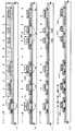
ここで、アクティブマトリクス型液晶表示装置の構成の一例を図15に示す。図15は、説明の便宜上、アクティブマトリクス型液晶表示装置のアクティブマトリクス基板のみが示されており、対向基板は省略されている。5001はアクティブマトリクス基板、5002および5003はソースドライバ、5004および5005はゲートドライバ、5006は画素部である。なお、アクティブマトリクス基板5001は、ガラス基板や石英基板などの絶縁基板をベースとしている。
【0014】
また、より複雑な構成をとるアクティブマトリクス型液晶表示装置においては、図15の5007〜5010に示す様な位置に、他の駆動回路が配置されることが検討されている。他の駆動回路回路は、プロセッサー回路の様な複雑なロジック回路やメモリ回路の様な面積の広い回路で構成されるため、駆動回路全体の占有面積は大きくなると予想される。
【0015】
以上の様に、一般的には1枚の絶縁基板上にアクティブマトリクス回路5001、ソースドライバ5002ならびに5003、ゲートドライバ5004ならびに5005、および他の駆動回路を配置する構成となる。従って、決められた基板サイズ上で表示領域をできるだけ多く確保するためには、画素部以外の占有面積を可能な限り小さくする必要がある。
【0016】
しかしながら、図15に示す様な従来構造をとる場合、画素部以外の占有面積を小さくすることには限界があり、このことがアクティブマトリクス型液晶表示装置の小型化を妨げる問題の一つとなっている。
【0017】
そこで、本出願人による特許出願である特開平10−104663号公報には、上述のドライバ等の占有面積の問題を解決する技術が開示されている。特開平10−104663号公報には、画素部、駆動回路、および他のコントロール回路(他の駆動回路)を1枚の絶縁基板上に集積化する反射型のアクティブマトリクス型液晶表示装置を構成するに際し、駆動回路および他のコントロール回路を画素部の領域内に形成する構成が開示されている。
【0018】
特開平10−104663号公報によると、何れの実施例においても、画素部の画素TFTに接続されている反射画素電極の下部にドライバ回路やコントロール回路を構成するTFTが配置されることが開示されている。また、ドライバ回路やコントロール回路を構成するための配線がBM(ブラックマスク)配線と同じ層に形成される様子が示されている。
【0019】
しかし、特開平10−104663号公報に開示されている構造では、ドライバ回路やコントロール回路に流れるクロック信号やデータ信号などがBM配線層に流れ、BM配線層に生じる電気ノイズが画素電極に悪影響を及ぼすことになる。この電気ノイズが液晶分子の挙動に影響を及ぼすことがあり、表示画像の乱れが生じることがある。
【0020】
また、従来のアクティブマトリクス型液晶表示装置には、次のような問題もあった。
【0021】
画素TFTと駆動回路を構成するTFTとでは動作条件が同一でなく、それぞれのTFTに要求される特性は少なからず異なっている。例えば、画素TFTはスイッチ素子として機能するものであり、液晶に電圧を印加して駆動させるものである。液晶は交流で駆動させるので、フレーム反転駆動と呼ばれる方式が多く採用されている。この方式では消費電力を低く抑えるために、画素TFTに要求される特性はオフ電流値(TFTがオフ動作時に流れるドレイン電流)を十分低くすることである。一方、駆動回路のバッファ回路は高い駆動電圧が印加されるため、高電圧が印加されても壊れないように耐圧を高めておく必要がある。また電流駆動能力を高めるために、オン電流値(TFTがオン動作時に流れるドレイン電流)を十分確保する必要がある。
【0022】
オフ電流値を低減するためのTFTの構造として、低濃度ドレイン(LDD:Lightly Doped Drain)構造が知られている。この構造はチャネル形成領域と、高濃度に不純物元素を添加して形成するソース領域またはドレイン領域との間に低濃度に不純物元素を添加した領域を設けたものであり、この領域をLDD領域と呼んでいる。また、ホットキャリアによるオン電流値の劣化を防ぐための手段として、LDD領域をゲート絶縁膜を介してゲート電極と重ねて配置させた、いわゆるGOLD(Gate-drain Overlapped LDD)構造が知られている。このような構造とすることで、ドレイン近傍の高電界が緩和されてホットキャリア注入を防ぎ、劣化現象の防止に有効であることが知られている。
【0023】
一方、アクティブマトリクス型液晶表示装置の商品としての価値を高めるために、画面の大型化および高精細化が要求がなされている。しかし、画面の大型化および高精細化により走査線(ゲート配線)の数が増えその長さも増大するので、ゲート配線の低抵抗化がより必要となる。すなわち走査線が増えるに従って液晶への充電時間が短くなり、ゲート配線の時定数(抵抗×容量)を小さくして高速で応答させる必要がある。例えば、ゲート配線を形成する材料の比抵抗が100μΩcmの場合には画面サイズが6インチクラスがほぼ限界となるが、3μΩcmの場合には27インチクラス相当まで表示が可能とされている。
【0024】
しかしながら、画素部の画素TFTと、シフトレジスタ回路やバッファ回路などの駆動回路のTFTとでは、その要求される特性は必ずしも同じではない。例えば、画素TFTにおいてはゲートに大きな逆バイアス(nチャネル型TFTでは負の電圧)が印加されるが、駆動回路のTFTは基本的に逆バイアス状態で動作することはない。また、動作速度に関しても、画素TFTは駆動回路のTFTの1/100以下で良い。
【0025】
また、GOLD構造はオン電流値の劣化を防ぐ効果は高いが、その反面、通常のLDD構造と比べてオフ電流値が大きくなってしまう問題があった。従って、画素TFTに適用するには好ましい構造ではなかった。逆に通常のLDD構造はオフ電流値を抑える効果は高いが、ドレイン近傍の電界を緩和してホットキャリア注入による劣化を防ぐ効果は低かった。このように、アクティブマトリクス型液晶表示装置のような動作条件の異なる複数の集積回路を有する半導体表示装置において、全てのTFTを同じ構造で形成することは必ずしも好ましくなかった。このような問題点は、特に結晶質シリコンTFTにおいて、その特性が高まり、またアクティブマトリクス型液晶表示装置に要求される性能が高まるほど顕在化してきた。
【0026】
また、大画面のアクティブマトリクス型の液晶表示装置を実現するために、配線材料としてアルミニウム(Al)や銅(Cu)を使用することも考えられるが、耐食性や耐熱性が悪いといった欠点があった。従って、TFTのゲート電極をこのような材料で形成することは必ずしも好ましくなく、そのような材料をTFTの製造工程に導入することは容易ではなかった。勿論、配線を他の導電性材料で形成することも可能であるが、アルミニウム(Al)や銅(Cu)ほど低抵抗な材料はなく、大画面の表示装置を作製することは困難であった。
【0027】
そこで、本発明は上記の問題を鑑みてなされたものであり、上述のドライバ等の占有面積の問題を解決し、かつ良好な表示画像を提供することができる大画化可能な反射型液晶表示装置を提供することを目的とする。
【0028】
【課題を解決するための手段】
【0029】
本発明は、アクティブマトリクス回路、ソースドライバおよびゲートドライバ等の駆動回路、および他の駆動回路を1枚の絶縁基板上に集積化する反射型のアクティブマトリクス型液晶表示装置を構成するに際し、画素部と駆動回路および他の駆動回路とを重ならせる。なお、本明細書においては、ソースドライバならびにゲートドライバ等の駆動回路および他の駆動回路をまとめて駆動回路という場合がある。
【0030】
本発明の構成はバックライト等からの光の光路(開口部)を確保する必要のある透過型のアクティブマトリクス型液晶表示装置では困難な構成である。なぜならば、透過型のアクティブマトリクス型液晶表示装置の画素部は、その殆どの領域が開口部であり、画素部において透過光量を落とさずに駆動回路を構成するのは困難であるからである。
【0031】
そこで、本発明はバックライトからの光の光路を確保する必要のない反射型のアクティブマトリクス型液晶表示装置において、光の反射板となる画素電極の下方に駆動回路を配置しようとするものである。
【0032】
以下に本発明の構成を記載する。
【0033】
請求項1に記載の発明によると、
マトリクス状に配置された複数の画素TFTおよび前記複数の画素TFTのそれぞれのソース電極またはドレイン電極に接続された反射電極を有する画素部と、
複数の駆動回路TFTを有する駆動回路と、
を有する反射型半導体表示装置において、
前記画素TFTおよび前記駆動回路TFTは、第1の導電層で形成されるゲート電極を有しており、
前記ゲート電極は、第2の導電層で形成されるゲート配線と接続部で電気的に接触しており、
前記接続部は、前記画素TFTと前記駆動回路のTFTとが有するチャネル形成領域の外側に設けられており、
前記駆動回路の一部または全部は、前記反射電極の下部に配置され、
前記駆動回路の電源線は、前記反射電極と前記前記画素TFTおよび前記駆動回路TFTのソース電極またはドレイン電極との間に形成されることを特徴とする反射型半導体表示装置が提供される。
【0034】
また、請求項2に記載の発明によると、
マトリクス状に配置された複数の画素TFTおよび前記複数の画素TFTのそれぞれのソース電極またはドレイン電極に接続された反射電極を有する画素部と、
複数の駆動回路TFTを有する駆動回路と、
を有する反射型半導体表示装置において、
前記画素TFTおよび前記駆動回路TFTは、第1の導電層で形成されるゲート電極を有しており、
前記ゲート電極は、第2の導電層で形成されるゲート配線と、前記画素TFTと前記駆動回路のTFTとが有するチャネル形成領域の外側に設けられた接続部で電気的に接触しており、
前記画素TFTのLDD領域は、前記画素TFTのゲート電極と重ならないように配置され、
前記駆動回路の第1のnチャネル型TFTのLDD領域は、前記第1のnチャネル型TFTのゲート電極と重なるように配置され、
前記駆動回路の第2のnチャネル型TFTのLDD領域は、前記第1のnチャネル型TFTのゲート電極と少なくとも一部が重なるように配置されており、
前記駆動回路の一部または全部は、前記反射電極の下部に配置され、
前記駆動回路の電源線は、前記反射電極と前記前記画素TFTおよび前記駆動回路TFTのソース電極またはドレイン電極との間に形成されることを特徴とする反射型半導体表示装置が提供される。
【0035】
また、請求項3に記載の発明によると、
画素部と駆動回路とを同一の基板上に有する反射型半導体表示装置において、
前記画素部には、LDD領域がゲート電極と重ならないように設けられた画素TFTおよび前記画素TFTのそれぞれのソース電極またはドレイン電極に接続された反射電極を有しており、
前記駆動回路には、LDD領域の全部がゲート電極と重なるように設けた第1のnチャネル型TFTと、LDD領域の一部がゲート電極と重なるように設けた第2のnチャネル型TFTとを有しており、
前記画素TFTと、前記第1および第2のnチャネル型TFTのゲート電極は、第1の導電層で形成され、前記ゲート電極に接続するゲート配線は第2の導電層で形成され、
前記ゲート電極と前記ゲート配線とは、前記画素TFTと前記駆動回路のTFTとのチャネル形成領域の外側の接続部で電気的に接続しており、
前記駆動回路の一部または全部は、前記反射電極の下部に配置され、
前記駆動回路の電源線は、前記反射電極と前記前記画素TFTおよび前記駆動回路TFTのソース電極またはドレイン電極との間に形成されることを特徴とする反射型半導体表示装置が提供される。
【0036】
また、請求項1乃至請求項3のいずれか一において、前記画素部には、前記画素TFTのソースまたはドレイン領域に接続し一導電型の不純物元素を含む半導体層と、容量配線と、前記半導体層と前記容量配線との間の絶縁膜とで保持容量が形成され、前記容量配線は前記第1の導電層と前記第2の導電層とで形成されるようにしてもよい。
【0037】
また、請求項1乃至請求項4のいずれか一において、前記第1の導電層が、タンタル、タングステン、チタン、モリブデンから選ばれた少なくとも1種を主成分とし、前記第2の導電層が、アルミニウムまたは銅を主成分とするようにしてもよい。
【0038】
また、請求項1乃至請求項4のいずれか一において、前記第1の導電層は、タンタル、タングステン、チタン、モリブデンから選ばれた少なくとも1種と窒素とを含む導電層(A)と、前記導電層(A)上に形成され、タンタル、タングステン、チタン、モリブデンから選ばれた少なくとも1種を主成分とする導電層(B)と、前記導電層(B)が前記導電層(A)に接しない領域に形成され、タンタル、タングステン、チタン、モリブデンから選ばれた少なくとも1種と窒素とを含む導電層(C)とを有し、前記第2の導電層は、少なくとも、アルミニウムまたは銅を主成分とする導電層(D)と、タンタル、タングステン、チタン、モリブデンから選ばれた少なくとも1種を主成分とする導電層(E)とを有するようにしてもよい。
【0039】
また、請求項1乃至請求項4のいずれか一において、前記第1の導電層は、タンタル、タングステン、チタン、モリブデンから選ばれた少なくとも1種と窒素とを含む導電層(A)と、前記導電層(A)上に形成され、タンタル、タングステン、チタン、モリブデンから選ばれた少なくとも1種を主成分とする導電層(B)と、前記導電層(B)が前記導電層(A)に接しない領域に形成され、タンタル、タングステン、チタン、モリブデンから選ばれた少なくとも1種と窒素とを含む導電層(C)とを有し、前記第2の導電層は、少なくとも、アルミニウムまたは銅を主成分とする導電層(D)と、タンタル、タングステン、チタン、モリブデンから選ばれた少なくとも1種を主成分とする導電層(E)とを有し、前記接続部で導電層(C)と導電層(D)が接触しているようにしてもよい。
【0040】
請求項6または請求項7において、前記導電層(B)は、添加元素としてアルゴンを含み、かつ、前記導電層(B)中の酸素濃度が30ppm以下であるようにしてもよい。
【0041】
【発明の実施の形態】
【0042】
図1を参照する。図1には、本発明の反射型液晶表示装置のアクティブマトリクス基板の上面図が示されている。説明の便宜上、図の一部分は透視図としている。また、説明の便宜上、対向基板は省略されている。
【0043】
図1に示される本発明の反射型液晶表示装置において、101はアクティブマトリクス基板、102および103はソースドライバ、104および105はゲートドライバ、106は画素部である。図1に示されるように、本発明の反射型液晶表示装置においては、ソースドライバ102ならびに103およびゲートドライバ104ならびに105は、画素部106の下部に形成されている。
【0044】
また、図1に示される本発明の反射型液晶表示装置は、ソースドライバ102の4つの端面のうち2つはアクティブマトリクス基板の端面に面しているが、残りの端面のうち一つはゲートドライバ105に面している。また同様に、ソースドライバ103の4つの端面のうち2つはアクティブマトリクス基板の端面に面しているが、残りの端面のうち一つはゲートドライバ104に面している。また同様に、ゲートドライバ104の4つの端面のうち2つはアクティブマトリクス基板の端面に面しているが、残りの端面のうち一つはソースドライバ102に面している。また同様に、ゲートドライバ105の4つの端面のうち2つはアクティブマトリクス基板の端面に面しているが、残りの端面のうち一つはソースドライバ103に面している。このようなドライバの配置によって、反射型のアクティブマトリクス型液晶表示装置の小型化が実現されている。
【0045】
また、図1においては示していないが、ソースドライバやゲートドライバ以外の他の駆動回路(メモリ、CPU、コントロール回路など)は、ソースドライバおよびゲートドライバが存在する以外の部分に形成されるようにしてもよい。
【0046】
このような回路配置をとることによって、小型な反射型液晶表示装置が実現できる。
【0047】
ここで、図2を参照する。図2には本発明の反射型液晶表示装置のある実施形態の断面図が示されている。基板200上に複数のTFTが形成されている。ここでは、画素部を構成するTFTを画素TFT204とし、ソースドライバやゲートドライバ等の駆動回路を構成するTFTを駆動回路TFT(Pチャネル型駆動回路TFT201、第1のNチャネル型駆動回路TFT202および第2のNチャネル型駆動回路TFT203)とする。また、205は保持容量である。
【0048】
図2に示される様に、画素TFT202のドレイン電極206に接続された画素電極207の下部に、駆動回路TFT(Pチャネル型駆動回路TFT201、第1のNチャネル型駆動回路TFT202および第2のNチャネル型駆動回路TFT203)が形成されている。
【0049】
また、図2に示される様に、本発明の反射型液晶表示装置は、駆動回路TFT(Pチャネル型駆動回路TFT201、第1のNチャネル型駆動回路TFT202および第2のNチャネル型駆動回路TFT203)の電源線(VDDまたはGND)が、第2層間膜208の上部に第3配線209、210および211として形成され、コンタクトホールを介してそれぞれPチャネル型駆動回路TFT201、第1のNチャネル型駆動回路TFT202および第2のNチャネル型駆動回路TFT203のソースまたはドレイン電極に接続されている。
【0050】
また、Pチャネル型駆動回路TFT201、第1のNチャネル型駆動回路TFT202および第2のNチャネル型駆動回路TFT203をそれぞれ接続したり、回路同士を接続する配線は、TFTのソース・ドレイン配線と同じ層またはTFTのゲート配線と同じ層に形成されている。このような構成をとることによって第3配線209、210および211には安定した電圧が供給され、クロック信号やデータ信号等の電気信号は供給されない。よって、第3配線209、210および211に供給される電圧によっては電気ノイズが発生しない。よって、第3配線209、210および211は上部の画素電極に及ぼす影響を極力小さくすることができる。
【0051】
また、駆動回路TFTによって構成される回路にクロック信号やデータ信号等の電気信号が供給され、電気ノイズが発生する。しかし、本発明の構成においては、この電気ノイズは安定した電圧が供給される第3配線がシールド線となり、画素電極に影響を及ぼすことはない。よって、数十MHzといったような高周波数のクロック信号によってドライバを駆動する場合でも、ドライバで発生する電気ノイズが画素電極に及ぼす影響を極力小さくすることができる。
【0052】
従って、本願発明によると、画素電極の下方に駆動回路を構成しても、画素電極に及ぼされる電気ノイズによる影響を極力抑えることができるので、良好な表示画像を得ることができる。
【0053】
なお、図2においては、Pチャネル型駆動回路TFT201、第1のNチャネル型駆動回路TFT202および第2のNチャネル型駆動回路TFT203の構造が示されているだけであるが、実際には、複数のNチャネル型駆動回路TFTと複数のPチャネル型駆動回路TFTとが電気的に接続され様々な回路を構成している。
【0054】
ここで、以下の実施例をもって、本発明を更に詳細に説明する。ただし、以下の実施例は、本発明のある実施形態に過ぎず、本発明が以下の実施例に限定されるわけではない。
【0055】
(実施例1)
【0056】
次に、図3〜図8を用いて、本実施例の反射型液晶表示装置の作製方法の一例について説明する。
【0057】
図3(A)において、基板1001には低アルカリガラス基板や石英基板を用いることができる。本実施例では低アルカリガラス基板を用いた。この場合、ガラス歪み点よりも10〜20℃程度低い温度であらかじめ熱処理しておいても良い。この基板1001のTFT形成表面には、基板1001からの不純物拡散を防ぐために、酸化シリコン膜、窒化シリコン膜または酸化窒化シリコン膜などの下地膜1002を形成する。例えば、プラズマCVD法でSiH4、NH3、N2Oから作製される酸化窒化シリコン膜を100nm、同様にSiH4、N2Oから作製される酸化窒化シリコン膜を200nmの厚さに積層形成する。
【0058】
次に、20〜150nm(好ましくは30〜80nm)の厚さで非晶質構造を有する半導体膜1003aを、プラズマCVD法やスパッタ法などの公知の方法で形成する。本実施例では、プラズマCVD法で非晶質シリコン膜を55nmの厚さに形成した。非晶質構造を有する半導体膜としては、非晶質半導体膜や微結晶半導体膜があり、非晶質シリコンゲルマニウム膜などの非晶質構造を有する化合物半導体膜を適用しても良い。また、下地膜1002と非晶質シリコン膜1003aとは同じ成膜法で形成することが可能であるので、両者を連続形成しても良い。その場合、下地膜を形成した後、一旦大気雰囲気に晒すことがなくその表面の汚染を防ぐことが可能となり、作製するTFTの特性バラツキやしきい値電圧の変動を低減させることができる(図3(A))。
【0059】
そして、公知の結晶化技術を使用して非晶質シリコン膜1003aから結晶質シリコン膜1003bを形成する。例えば、レーザー結晶化法や熱結晶化法(固相成長法)を適用すれば良いが、ここでは、特開平7−130652号公報で開示された技術に従って、触媒元素を用いる結晶化法で結晶質シリコン膜1003bを形成した。結晶化の工程に先立って、非晶質シリコン膜の含有水素量にもよるが、400〜500℃で1時間程度の熱処理を行い、含有水素量を5atom%以下にしてから結晶化させることが望ましい。非晶質シリコン膜を結晶化させると原子の再配列が起こり緻密化するので、作製される結晶質シリコン膜の厚さは当初の非晶質シリコン膜の厚さ(本実施例では55nm)よりも1〜15%程度減少する(図1(B))。
【0060】
そして、結晶質シリコン膜1003bを島状にパターンニングして、島状半導体層1004〜1007を形成する。その後、プラズマCVD法またはスパッタ法により50〜100nmの厚さの酸化シリコン膜によるマスク層1008を形成する(図3(C))。
【0061】
そしてレジストマスク1009を設け、nチャネル型TFTを形成することとなる島状半導体層1005〜1007の全面に1×10¹⁶〜5×10¹⁷atoms/cm3程度の濃度でp型を付与する不純物元素としてボロン(B)を添加する。このボロン(B)の添加は、しきい値電圧を制御する目的でなされる。ボロン(B)の添加はイオンドープ法で実施しても良いし、非晶質シリコン膜を成膜するときに同時に添加しておくこともできる。ここでのボロン(B)添加は必ずしも必要ではない(図3(D))。
【0062】
ドライバ等の駆動回路のnチャネル型TFTのLDD領域を形成するために、n型を付与する不純物元素を島状半導体層1010、1011に選択的に添加する。そのため、あらかじめレジストマスク1013〜1016を形成する。n型を付与する不純物元素としては、リン(P)や砒素(As)を用いれば良く、ここではリン(P)を添加すべく、フォスフィン(PH3)を用いたイオンドープ法を適用した。形成された不純物領域1017、1018のリン(P)濃度は2×10¹⁶〜5×10¹⁹atoms/cm3の範囲とすれば良い。本明細書中では、ここで形成された不純物領域1017〜1019に含まれるn型を付与する不純物元素の濃度を(n-)と表す。また、不純物領域1019は、画素部の保持容量を形成するための半導体層であり、この領域にも同じ濃度でリン(P)を添加する(図4(A))。その後、レジストマスク1013〜1016を除去する。
【0063】
次に、マスク層1008をフッ酸などにより除去した後、図3(D)と図4(A)で添加した不純物元素を活性化させる工程を行う。活性化は、窒素雰囲気中で500〜600℃で1〜4時間の熱処理や、レーザー活性化の方法により行うことができる。また、両者を併用して行っても良い。本実施例では、レーザー活性化の方法を用いる。レーザー光にはKrFエキシマレーザー光(波長248nm)を用いる。本実施例では、レーザー光の形状を線状ビームに加工して用い、発振周波数5〜50Hz、エネルギー密度100〜500mJ/cm2として線状ビームのオーバーラップ割合を80〜98%で走査することによって島状半導体層が形成された基板全面を処理する。尚、レーザー光の照射条件には何ら限定される事項はなく、実施者が適宣決定すれば良い。
【0064】
そして、ゲート絶縁膜1020をプラズマCVD法またはスパッタ法を用いて10〜150nmの厚さでシリコンを含む絶縁膜で形成する。例えば、120nmの厚さで酸化窒化シリコン膜を形成する。ゲート絶縁膜には、他のシリコンを含む絶縁膜を単層または積層構造として用いても良い(図4(B))。
【0065】
次に、ゲート電極を形成するために第1の導電層を成膜する。この第1の導電層は単層で形成しても良いが、必要に応じて二層あるいは三層といった積層構造としても良い。本実施例では、導電性の窒化物金属膜から成る導電層(A)1021と金属膜から成る導電層(B)1022とを積層させる。導電層(B)1022はタンタル(Ta)、チタン(Ti)、モリブデン(Mo)、タングステン(W)から選ばれた元素、または前記元素を主成分とする合金か、前記元素を組み合わせた合金膜(代表的にはMo−W合金膜、Mo−Ta合金膜)で形成すれば良く、導電層(A)1021は窒化タンタル(TaN)、窒化タングステン(WN)、窒化チタン(TiN)膜、窒化モリブデン(MoN)で形成する。また、導電層(A)1021は代替材料として、タングステンシリサイド、チタンシリサイド、モリブデンシリサイドを適用しても良い。導電層(B)は低抵抗化を図るために含有する不純物濃度を低減させると良く、特に酸素濃度に関しては30ppm以下とすると良かった。例えば、タングステン(W)は酸素濃度を30ppm以下とすることで20μΩcm以下の比抵抗値を実現することができる。
【0066】
導電層(A)1021は10〜50nm(好ましくは20〜30nm)とし、導電層(B)1022は200〜400nm(好ましくは250〜350nm)とすれば良い。本実施例では、導電層(A)1021に30nmの厚さの窒化タンタル膜を、導電層(B)1022には350nmのTa膜を用い、いずれもスパッタ法で形成した。このスパッタ法による成膜では、スパッタ用のガスのArに適量のXeやKrを加えておくと、形成する膜の内部応力を緩和して膜の剥離を防止することができる。尚、図示しないが、導電層(A)1021の下に2〜20nm程度の厚さでリン(P)をドープしたシリコン膜を形成しておくことは有効である。これにより、その上に形成される導電膜の密着性向上と酸化防止を図ると同時に、導電層(A)または導電層(B)が微量に含有するアルカリ金属元素がゲート絶縁膜1020に拡散するのを防ぐことができる(図4(C))。
【0067】
次に、レジストマスク1023〜1027を形成し、導電層(A)1021と導電層(B)1022とを一括でエッチングしてゲート電極1028〜1031と容量配線1032を形成する。ゲート電極1028〜1031と容量配線1032は、導電層(A)から成る1028a〜1032aと、導電層(B)から成る1028b〜1032bとが一体として形成されている。この時、後にドライバ等の駆動回路を構成するTFTのゲート電極1029、1030は不純物領域1017、1018の一部と、ゲート絶縁膜1020を介して重なるように形成する(図4(D))。
【0068】
次いで、ドライバのPチャネル型TFTのソース領域およびドレイン領域を形成するために、P型を付与する不純物元素を添加する工程を行う。ここでは、ゲート電極1028をマスクとして、自己整合的に不純物領域を形成する。このとき、Nチャネル型TFTが形成される領域はレジストマスク1033で被覆しておく。そして、ジボラン(B2H6)を用いたイオンドープ法で不純物領域1034を形成した。この領域のボロン(B)濃度は3×10²⁰〜3×10²¹atoms/cm3となるようにする。本明細書中では、ここで形成された不純物領域1034に含まれるP型を付与する不純物元素の濃度を(p+)と表す(図5(A))。
【0069】
次に、Nチャネル型TFTにおいて、ソース領域またはドレイン領域として機能する不純物領域の形成を行った。レジストのマスク1035〜1037を形成し、N型を付与する不純物元素を添加して不純物領域1038〜1042を形成した。これは、フォスフィン(PH3)を用いたイオンドープ法で行い、この領域のリン(P)濃度を1×10²⁰〜1×10²¹atoms/cm3とした。本明細書中では、ここで形成された不純物領域1038〜1042に含まれるN型を付与する不純物元素の濃度を(n+)と表す(図5(B))。
【0070】
不純物領域1038〜1042には、既に前工程で添加されたリン(P)またはボロン(B)が含まれているが、それに比して十分に高い濃度でリン(P)が添加されるので、前工程で添加されたリン(P)またはボロン(B)の影響は考えなくても良い。また、不純物領域1038に添加されたリン(P)濃度は図5(A)で添加されたボロン(B)濃度の1/2〜1/3なのでp型の導電性が確保され、TFTの特性に何ら影響を与えることはなかった。
【0071】
そして、画素マトリクス回路のnチャネル型TFTのLDD領域を形成するためのn型を付与する不純物添加の工程を行った。ここではゲート電極1031をマスクとして自己整合的にn型を付与する不純物元素をイオンドープ法で添加する。添加するリン(P)の濃度は1×10¹⁶〜5×10¹⁸atoms/cm3であり、図4(A)および図5(A)と図5(B)で添加する不純物元素の濃度よりも低濃度で添加することで、実質的には不純物領域1043、1044のみが形成される。本明細書中では、この不純物領域1043、1044に含まれるn型を付与する不純物元素の濃度を(n--)と表す(図5(C))。
【0072】
その後、それぞれの濃度で添加されたn型またはp型を付与する不純物元素を活性化するために熱処理工程を行う。この工程はファーネスアニール法、レーザーアニール法、またはラピッドサーマルアニール法(RTA法)で行うことができる。ここではファーネスアニール法で活性化工程を行った。熱処理は酸素濃度が1ppm以下、好ましくは0.1ppm以下の窒素雰囲気中で400〜800℃、代表的には500〜600℃で行うものであり、本実施例では550℃で4時間の熱処理を行った。また、基板1001に石英基板のような耐熱性を有するものを使用した場合には、800℃で1時間の熱処理としても良く、不純物元素の活性化と、該不純物元素が添加された不純物領域とチャネル形成領域との接合を良好に形成することができる。
【0073】
この熱処理において、ゲート電極1028〜1031と容量配線1032を形成する金属膜1028b〜1032bは、表面から5〜80nmの厚さで導電層(C)1028c〜1032cが形成される。例えば、導電層(B)1028b〜1032bがタングステン(W)の場合には窒化タングステン(WN)が形成され、タンタル(Ta)の場合には窒化タンタル(TaN)を形成することができる。また、導電層(C)1028c〜1032cは、窒素またはアンモニアなどを用いた窒素を含むプラズマ雰囲気にゲート電極1028〜1031を晒しても同様に形成することができる。さらに、3〜100%の水素を含む雰囲気中で、300〜450℃で1〜12時間の熱処理を行い、島状半導体層を水素化する工程を行った。この工程は熱的に励起された水素により半導体層のダングリングボンドを終端する工程である。水素化の他の手段として、プラズマ水素化(プラズマにより励起された水素を用いる)を行っても良い。
【0074】
島状半導体層が、非晶質シリコン膜から触媒元素を用いる結晶化の方法で作製された場合、島状半導体層中には微量の触媒元素が残留する。勿論、そのような状態でもTFTを完成させることが可能であるが、残留する触媒元素を少なくともチャネル形成領域から除去する方がより好ましい。この触媒元素を除去する手段の一つにリン(P)によるゲッタリング作用を利用する手段がある。ゲッタリングに必要なリン(P)の濃度は図5(B)で形成した不純物領域(n+)と同程度であり、ここで実施される活性化工程の熱処理により、nチャネル型TFTおよびpチャネル型TFTのチャネル形成領域から触媒元素をゲッタリングをすることができた(図5(D))。
【0075】
活性化および水素化の工程が終了したら、ゲート配線とする第2の導電膜を形成する。この第2の導電膜は低抵抗材料であるアルミニウム(Al)や銅(Cu)を主成分とする導電層(D)と、にチタン(Ti)やタンタル(Ta)、タングステン(W)、モリブデン(Mo)から成る導電層(E)とで形成すると良い。本実施例では、チタン(Ti)を0.1〜2重量%含むアルミニウム(Al)膜を導電層(D)1045とし、チタン(Ti)膜を導電層(E)1046として形成した。導電層(D)1045は200〜400nm(好ましくは250〜350nm)とすれば良く、導電層(E)1046は50〜200(好ましくは100〜150nm)で形成すれば良い(図6(A))。
【0076】
そして、ゲート電極に接続するゲート配線を形成するために導電層(E)1046と導電層(D)1045とをエッチング処理して、ゲート配線1047、1048と容量配線1049を形成た。エッチング処理は最初にSiCl4とCl2とBCl3との混合ガスを用いたドライエッチング法で導電層(E)の表面から導電層(D)の途中まで除去し、その後リン酸系のエッチング溶液によるウエットエッチングで導電層(D)を除去することにより、下地との選択加工性を保ってゲート配線を形成することができる。
【0077】
図17には、図6(C)における、破線A−A’部の上面図が示されている。図17に示される様に、ゲート電極1028および1029はゲート配線1047の一部と重なり、電気的に接触している様子がわかる。
【0078】
第1の層間絶縁膜1050は500〜1500nmの厚さで酸化シリコン膜または酸化窒化シリコン膜で形成され、その後、それぞれの島状半導体層に形成されたソース領域またはドレイン領域に達するコンタクトホールを形成し、ソース配線1051〜1054と、ドレイン配線1055〜1058を形成する。図示していないが、本実施例ではこの電極を、Ti膜を100nm、Tiを含むアルミニウム膜300nm、Ti膜150nmをスパッタ法で連続して形成した3層構造の積層膜とした。
【0079】
次に、パッシベーション膜1059として、窒化シリコン膜、酸化シリコン膜、または窒化酸化シリコン膜を50〜500nm(代表的には100〜300nm)の厚さで形成する。この状態で水素化処理を行うとTFTの特性向上に対して好ましい結果が得られた。例えば、3〜100%の水素を含む雰囲気中で、300〜450℃で1〜12時間の熱処理を行うと良く、あるいはプラズマ水素化法を用いても同様の効果が得られた。なお、ここで後に画素電極とドレイン配線を接続するためのコンタクトホールを形成する位置において、パッシベーション膜1059に開口部を形成しておいても良い(図6(C))。
【0080】
その後、有機樹脂からなる第2層間絶縁膜1060を1.0〜1.5μmの厚さに形成する。有機樹脂としては、ポリイミド、アクリル、ポリアミド、ポリイミドアミド、BCB(ベンゾシクロブテン)等を使用することができる。ここでは、基板に塗布後、熱重合するタイプのポリイミドを用い、300℃で焼成して形成した。
【0081】
次に、第2層間絶縁膜にコンタクトホールを形成し、ドライバ等の駆動回路を構成するpチャネル型TFTおよびnチャネル型TFTのソースまたはドレイン電極に接続する第3配線1061、1062および1063を形成する(図7)。本実施例においては、第3配線1061、1062および1063には、ソース電極およびドレイン電極と同じ材料が用いられた。また、第3配線1061、1062および1063には、他の金属が用いられても良い。
【0082】
その後、有機樹脂からなる第3層間絶縁膜1064を1.0〜1.5μmの厚さに形成する。有機樹脂としては、第2層間絶縁膜と同様の樹脂をもちいることができる。ここでは、基板に塗布後、熱重合するタイプのポリイミドを用い、300℃で焼成して形成した。
【0083】
そして、第2層間絶縁膜1060および第3層間絶縁膜1064にドレイン配線1058に達するコンタクトホールを形成し、画素電極1065を形成する。本発明の反射型液晶表示装置においては、画素電極は金属膜を用いる。本実施例では、本実施例では、Ti膜を300nmに形成し、その後AlとTiの合金膜を100nmに形成した(図7)。
【0084】
こうして同一基板上に、駆動回路TFTと画素部の画素TFTとを有した基板を完成させることができた。駆動回路にはpチャネル型TFT801、第1のnチャネル型TFT802、第2のnチャネル型TFT803、画素部には画素TFT804、保持容量805が形成されている。本明細書では便宜上このような基板をアクティブマトリクス基板と呼んでいる。
【0085】
次に、上記の工程によって作製されたアクティブマトリクス基板をもとに、反射型液晶表示装置を作製する工程を説明する。
【0086】
図7の状態のアクティブマトリクス基板に配向膜1066を形成する。本実施例では、配向膜1066にはポリイミドを用いた。次に、対向基板を用意する。対向基板は、ガラス基板1067、透明導電膜からなる対向電極1068、配向膜1069とで構成される。
【0087】
なお、本実施例では、配向膜には、液晶分子が基板に対して平行に配向するようなポリイミド膜を用いた。なお、配向膜形成後、ラビング処理を施すことにより、液晶分子がある一定のプレチルト角を持って平行配向するようにした。
【0088】
次に、上記の工程を経たアクティブマトリクス基板と対向基板とを公知のセル組み工程によって、シール材やスペーサ(共に図示せず)などを介して貼り合わせる。その後、両基板の間に液晶1070を注入し、封止剤(図示せず)によって完全に封止する。よって、図8に示すような反射型液晶表示装置が完成する。
【0089】
なお本実施例では、反射型液晶表示装置がTN(ツイスト)モードによって表示を行うようにした。そのため、偏光板(図示せず)が反射型液晶表示装置の上部に配置された。
【0090】
駆動回路のpチャネル型TFT801には、島状半導体層1004にチャネル形成領域806、ソース領域807a、807b、ドレイン領域808a,808bを有している。第1のnチャネル型TFT802には、島状半導体層1005にチャネル形成領域809、ゲート電極1029と重なるLDD領域810(以降、このようなLDD領域をLovと記す)、ソース領域811、ドレイン領域812を有している。このLov領域のチャネル長方向の長さは0.5〜3.0μm、好ましくは1.0〜1.5μmとした。第2のnチャネル型TFT803には、島状半導体層1006にチャネル形成領域813、LDD領域814、815、ソース領域816、ドレイン領域817を有している。このLDD領域はLov領域とゲート電極1030と重ならないLDD領域(以降、このようなLDD領域をLoffと記す)とが形成され、このLoff領域のチャネル長方向の長さは0.3〜2.0μm、好ましくは0.5〜1.5μmである。画素TFT804には、島状半導体層1007にチャネル形成領域818、819、Loff領域820〜823、ソースまたはドレイン領域824〜826を有している。Loff領域のチャネル長方向の長さは0.5〜3.0μm、好ましくは1.5〜2.5μmである。さらに、容量配線132、149と、ゲート絶縁膜と同じ材料から成る絶縁膜と、画素TFT804のドレイン領域826に接続し、n型を付与する不純物元素が添加された半導体層827とから保持容量805が形成されている。図8では画素TFT804をダブルゲート構造としたが、シングルゲート構造でも良いし、複数のゲート電極を設けたマルチゲート構造としても差し支えない。
【0091】
以上の様に本発明は、画素TFTおよびドライバが要求する仕様に応じて各回路を構成するTFTの構造を最適化し、液晶表示装置の動作性能と信頼性を向上させることを可能とすることができる。さらにゲート電極を耐熱性を有する導電性材料で形成することによりLDD領域やソース領域およびドレイン領域の活性化を容易とし、ゲート配線を低抵抗材料で形成することにより、配線抵抗を十分低減できる。従って、画素部(画面サイズ)が4インチクラス以上の表示装置にも適用することができる。
【0092】
(実施例2)
【0093】
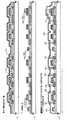
図9を参照する。図9には、本発明の反射型液晶表示装置のアクティブマトリクス基板の上面図が示されている。説明の便宜上、図の一部分は透視図としている。また、説明の便宜上、対向基板は省略されている。
【0094】
図9に示される本発明の反射型液晶表示装置において、901はアクティブマトリクス基板、902および903はソースドライバ、904はゲートドライバ、905はデジタルビデオデータ分割回路、906は画素部、907はFPC端子である。
【0095】
本実施例の反射型液晶表示装置においても、ソースドライバ、ゲートドライバおよびデジタルビデオデータ分割回路等の駆動回路が画素部の画素電極の下部に配置されている。
【0096】
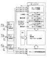
図10を参照する。図10には、本実施例の反射型液晶表示装置の回路ブロック図が示されている。ソースドライバ901は、DFF回路(レジスタ回路)901−1、ラッチ回路901−2、セレクタ回路(1)901−3、D/A変換回路901−4、セレクタ回路(2)901−5を有している。その他、バッファ回路やレベルシフタ回路(いずれも図示せず)を有している。また、説明の便宜上、D/A変換回路901−4にはレベルシフタ回路が含まれている。
【0097】
また、903はゲイトドライバであり、シフトレジスタ回路、バッファ回路、レベルシフタ回路等(いずれも図示せず)を有している。
【0098】
画素部904は、640×RGB×480の画素を有している。各画素には画素TFTが配置されており、各画素TFTのソース領域にはソース信号線が、ゲート電極にはゲート信号線が電気的に接続されている。また、各画素TFTのドレイン領域には画素電極が電気的に接続されている。各画素TFTは、各画素TFTに電気的に接続された画素電極への映像信号(階調電圧)の供給を制御している。各画素電極に映像信号(階調電圧)が供給され、各画素電極と対向電極との間に挟まれた液晶に電圧が印加され液晶が駆動される。
【0099】
905はデジタルビデオデータ分割回路(SPC;Serial-to-Parallel Conversion Circuitと呼ぶこともある)である。905−R、905−G、905−Bには、それぞれ、赤、緑、青の映像に対応するデジタルビデオデータが入力される。デジタルビデオデータ分割回路905は、外部から入力されるデジタルビデオデータの周波数を1/xに落とすための回路である(xは2以上の自然数)。外部から入力されるデジタルビデオデータを分割することにより、駆動回路の動作に必要な信号の周波数も1/xに落とすことができる。本実施例の液晶表示装置においては、デジタルビデオデータ分割回路905は、外部から入力される80MHzの8ビットデジタルビデオデータを10MHzに落としソースドライバに出力する。
【0100】
本実施例の反射型液晶表示装置によると、ソースドライバおよびゲートドライバだけでなく、デジタルビデオデータ分割回路をも画素部の画素電極下部に設けることができる。このように、本発明は、駆動回路の面積が大きいデジタルドライバに特に有利であることがわかる。
【0101】
また、本実施例の反射型液晶表示装置には、イメージセンサ等の素子を一体形成しても良い。
【0102】
(実施例3)
【0103】
図11を参照する。図11には、本発明の反射型液晶表示装置のアクティブマトリクス基板の上面図が示されている。説明の便宜上、図の一部分は透視図としている。また、説明の便宜上、対向基板は省略されている。
【0104】
図11に示される本発明の反射型液晶表示装置において、1101はアクティブマトリクス基板、1102および1103はソースドライバ、1104、1105および1106はゲートドライバ、1107は画素部、1108はFPC端子である。
【0105】
図11に示すように、本発明の反射型アクティブマトリクス型液晶表示装置においては、比較的自由にドライバ回路を配置することができる。本実施例のドライバの配置によると、アクティブマトリクス回路の駆動を分割し、時分割駆動、多点同時駆動も可能となる。
【0106】
(実施例4)
【0107】
本実施例の反射型液晶表示装置の断面図を図12に示す。本実施例の反射型液晶表示装置においては、アクティブマトリクス基板上に形成されたTFTが逆スタガ型の構造をとっている。
【0108】
基板2001は絶縁表面を有するものであり、ガラス基板、石英基板、プラスチック基板などの絶縁基板の他に、表面に絶縁被膜が形成された金属基板、シリコン基板、或いはセラミック基板などを適用することが可能である。ガラス基板は、例えばコーニング社の#1737基板に代表されるような、低アルカリガラス基板を適用することが望ましい。さらに、その表面に酸化シリコンまたは窒化シリコンを主成分として含む絶縁膜が密接形成されていると好ましい。図12には、この基板2001上に形成された画素部のnチャネル型TFT2052、保持容量2053、ドライバ等の駆動回路のnチャネル型TFT2051ならびにpチャネル型TFT2050が示されている。
【0109】
ゲート電極2002〜2005はアルミニウム(Al)、チタン(Ti)、タンタル(Ta)、クロム(Cr)、モリブデン(Mo)、タングステン(W)、ニッケル(Ni)、銅(Cu)から選ばれた一種または複数種の元素を含む材料から形成され、端面がテーパー形状となるようにパターン形成する。また、図示していないが、前記材料の積層構造としても良い。例えば、基板側から窒化タンタル(TaN)とTaの2層構造としても良い。さらに、ゲート電極の表面に陽極酸化法などで酸化物を被覆形成しておいても良い。
【0110】
ゲート電極を覆って形成するゲート絶縁膜は、窒化シリコン膜2006と酸化シリコン膜2007とから形成されている。ここでは2層構造で示したが、1層構造としても良いし、前記材料に限定される必要はない。ゲート絶縁膜の厚さは20〜200nm、好ましくは70〜150nmとすると良い。
【0111】
基板2001側からゲート電極、ゲート絶縁膜の順に形成した後に、TFTの活性層には結晶性半導体膜を適用し島状にパターン形成する。結晶質半導体膜の作製方法に特に限定はないが、非晶質シリコン膜をレーザー結晶化技術または熱結晶化技術、或いは非晶質シリコンの結晶化を助長する触媒元素を用いる結晶化の技術で作製した結晶質シリコン膜を用いることが最も望ましい。勿論、他の半導体材料で代用することも可能である。活性層の厚さは20〜150nm、好ましくは30〜75nmで形成する。
【0112】
駆動回路のpチャネル型TFT2050の活性層には、チャネル形成領域2009、ソース領域2010、ドレイン領域2011が形成されている。nチャネル型TFT2051の活性層には、チャネル形成領域2012、ソース領域2015、ドレイン領域2016、LDD領域2013、2014が形成されている。このLDD領域2013、2014にはn型を付与する不純物元素が5×10¹⁷〜5×1018cm−3の濃度で含まれている。n型を付与する不純物元素には、半導体技術の分野で周知のものであれば良く、代表的にはリン(P)や砒素(As)などを用いれば良い。LDD領域2013、2014はゲート電極2003とゲート絶縁膜とを介して重なるように設けられたGOLD構造となっている。
【0113】
画素部のnチャネル型TFT(画素TFT)2052の活性層にはチャネル形成領域2017、2022、ソースまたはドレイン領域2020、2021、2025、LDD領域2018a、2018b、2019a、2019b、2023a、2023b、2024a、2024bが設けられている。このLDD領域のn型を付与する不純物濃度は1×10¹⁷〜2.5×1018cm−3の範囲にすれば良いが、駆動回路のnチャネル型TFTのLDD領域2013、2014の不純物濃度よりも1/2から1/5の濃度とするのが好ましい。
【0114】
駆動回路のnチャネル型TFTのLDD領域は、ドレイン近傍の高電界を緩和してホットキャリア注入によるオン電流値の劣化を防ぐことを主な目的として設けるものであり、そのために適したn型を付与する不純物元素の濃度は5×10¹⁷〜5×1018cm-3とすれば良かった。一方、画素部のnチャネル型TFTのLDD領域は、オフ電流値を低減することを主たる目的とするために設けられる。
【0115】
この駆動回路のnチャネル型TFTのゲート電極と重なるLDD領域(以下、Lov領域という。尚、ov はoverlapの意味である。)のチャネル長方向の長さは、チャネル長3〜8μmに対して0.5〜3.0μm、好ましくは1.0〜1.5μmとすれば良い。また、画素部のnチャネル型TFTのゲート電極と重ならないLDD領域(以下、Loffという。尚、offとはoffsetの意味である。)のチャネル長方向の長さは0.5〜3.5μm、代表的には1.5〜2.5μmとすれば良い。
【0116】
チャネル保護膜2026〜2029は酸化シリコン膜などで形成され、図示するように活性層上にそのまま残しても良いが、第1の層間絶縁膜2030を形成する前に除去しても差し支えない。第1の層間絶縁膜2030は、窒化シリコン膜、酸化シリコン膜、窒化酸化シリコン膜またはそれらを組み合わせた積層構造で形成すれば良い。例えば、窒化酸化シリコン膜2030aと酸化シリコン膜2030bとすることができる。また、第1の層間絶縁膜の膜厚は500〜1500nmとすれば良い。
【0117】
第1の層間絶縁膜にはそれぞれのTFTのソースまたはドレイン領域に達するコンタクトホールが形成され、ソース配線2032、2034、2035とドレイン配線2033、2036が設けられる。図示していないがこの配線をTi膜を200nm、Tiを含有するAl膜を450nm、さらにTi膜を150nmの厚さで形成した3層積層構造としても良い。
【0118】
パッシベーション膜2037は、窒化シリコン膜、酸化シリコン膜、または窒酸化シリコン膜で30〜500nm、代表的には50〜200nmの厚さで形成する。さらに、第2の層間絶縁膜2038を約1000nmの厚さで形成する。第2の層間絶縁膜はポリイミド、ポリアミド、アクリル、ポリイミドアミド、ベンゾシクロブテンなどの有機樹脂膜を用いて形成すると良い。有機樹脂膜を用いることの利点は、膜の形成法が比較的簡便である点や、比誘電率が低いので寄生容量を低減できる点、さらに平坦性に優れる点などがある。例えば、塗布した後に熱重合するタイプのポリイミドを用いると、300℃程度で形成することができる。尚、上述した以外の有機樹脂膜や、有機系酸化シリコン化合物などを用いることも可能である。
【0119】
次に、第2層間絶縁膜2038およびパッシベーション膜2037にコンタクトホールを形成し、ドライバ等の駆動回路を構成するpチャネル型TFTおよびnチャネル型TFTのソースまたはドレイン電極に接続する第3配線2039および2040を形成する。本実施例においては、第3配線2039および2040には、ソース電極およびドレイン電極と同じ材料が用いられた。また、第3配線2039および2040には、他の金属が用いられても良い。
【0120】
その後、有機樹脂からなる第3層間絶縁膜2041を1.0〜1.5μmの厚さに形成する。有機樹脂としては、第2層間絶縁膜と同様の樹脂をもちいることができる。ここでは、基板に塗布後、熱重合するタイプのポリイミドを用い、300℃で焼成して形成する。
【0121】
そして、第3層間絶縁膜2041、第2層間絶縁膜2038およびパッシベーション膜2037にドレイン配線2036に達するコンタクトホールを形成し、画素電極2042を設ける。本発明の反射型液晶表示装置においては、画素電極は金属膜を用いる。本実施例では、Ti膜を300nmに形成し、その後AlとTiの合金膜を100nmに形成する。
【0122】
2044は対向基板、2045は対向電極、2046、2043は配向膜、2047は液晶である。
【0123】
(実施例5)
【0124】
上記実施例においては、ネマチック液晶を用いたTNモードとして用いられているが、他の表示モードなども用いることができる。
【0125】
さらに、応答速度の速い無しきい値反強誘電性液晶または強誘電性液晶を用いて、本発明のアクティブマトリクス型液晶表示装置を構成してもよい。
【0126】
本発明の反射型液晶表示装置には、TN液晶以外にも様々な液晶を用いることが可能である。例えば、1998, SID, "Characteristics and Driving Scheme of Polymer-Stabilized Monostable FLCD Exhibiting Fast Response Time and High Contrast Ratio with Gray-Scale Capability" by H. Furue et al.や、1997, SID DIGEST, 841, "A Full-Color Thresholdless Antiferroelectric LCD Exhibiting Wide Viewing Angle with Fast Response Time" by T. Yoshida et al.や、1996, J. Mater. Chem. 6(4), 671-673, "Thresholdless antiferroelectricity in liquid crystals and its application to displays" by S. Inui et al.や、米国特許第5594569 号に開示された液晶を用いることが可能である。
【0127】
ある温度域において反強誘電相を示す液晶を反強誘電性液晶という。反強誘電性液晶を有する混合液晶には、電場に対して透過率が連続的に変化する電気光学応答特性を示す、無しきい値反強誘電性混合液晶と呼ばれるものがある。この無しきい値反強誘電性混合液晶は、V字型の電気光学応答特性を示すものがあり、その駆動電圧が約±2.5V程度(セル厚約1μm〜2μm)のものも見出されている。
【0128】
ここで、V字型の電気光学応答を示す無しきい値反強誘電性混合液晶の印加電圧に対する光透過率の特性を示す例を図16に示す。図16に示すグラフの縦軸は透過率(任意単位)、横軸は印加電圧である。なお、液晶表示装置の入射側の偏光板の透過軸は、液晶表示装置のラビング方向にほぼ一致する無しきい値反強誘電性混合液晶のスメクティック層の法線方向とほぼ平行に設定されている。また、出射側の偏光板の透過軸は、入射側の偏光板の透過軸に対してほぼ直角(クロスニコル)に設定されている。
【0129】
図16に示されるように、このような無しきい値反強誘電性混合液晶を用いると、低電圧駆動かつ階調表示が可能となることがわかる。
【0130】
このような低電圧駆動の無しきい値反強誘電性混合液晶をアナログドライバを有する液晶表示装置に用いた場合には、画像信号のサンプリング回路の電源電圧を、例えば、5V〜8V程度に抑えることが可能となる。よって、ドライバの動作電源電圧を下げることができ、液晶表示装置の低消費電力化および高信頼性が実現できる。
【0131】
また、このような低電圧駆動の無しきい値反強誘電性混合液晶をデジタルドライバを有する液晶表示装置に用いた場合にも、D/A変換回路の出力電圧を下げることができるので、D/A変換回路の動作電源電圧を下げることができ、ドライバの動作電源電圧を低くすることができる。よって、液晶表示装置の低消費電力化および高信頼性が実現できる。
【0132】
よって、このような低電圧駆動の無しきい値反強誘電性混合液晶を用いることは、比較的LDD領域(低濃度不純物領域)の幅が小さなTFT(例えば、0nm〜500nmまたは0nm〜200nm)を用いる場合においても有効である。
【0133】
また、一般に、無しきい値反強誘電性混合液晶は自発分極が大きく、液晶自体の誘電率が高い。このため、無しきい値反強誘電性混合液晶を液晶表示装置に用いる場合には、画素に比較的大きな保持容量が必要となってくる。よって、自発分極が小さな無しきい値反強誘電性混合液晶を用いるのが好ましい。また、液晶表示装置の駆動方法を線順次駆動とすることにより、画素への階調電圧の書き込み期間(ピクセルフィードピリオド)を長くし、保持容量が小くてもそれを補うようにしてもよい。
【0134】
なお、このような無しきい値反強誘電性混合液晶を用いることによって低電圧駆動が実現されるので、液晶表示装置の低消費電力が実現される。
【0135】
なお、図16に示すような電気光学特性を有する液晶であれば、いかなるものも本発明の反射型液晶表示装置の表示媒体として用いることができる。
【0136】
また、本発明の半導体表示装置には、印加電圧に応答して光学的特性が変調され得るその他のいかなる表示媒体を用いてもよい。例えば、エレクトロルミネセンス素子などを用いても良い。
【0137】
(実施例6)
【0138】
本実施例では、本発明の反射型液晶表示装置にタッチパネルを組み合わせた例を示す。本実施例の反射型液晶表示装置には、上述の実施例の反射型液晶表示装置を用いることができる。
【0139】
ここで、図13を参照する。図13には、本実施例で用いるタッチパネルが示されている。図13に示すタッチパネルは、発光素子と受光素子とをパネル周囲に対向して設けられた光学式(又は光電式)のものである。図13(A)は正面図であり、図13(B)は図13(A)の一点鎖線A−A'に沿った断面図である。
【0140】
図13に示すように、パネル3000の1辺に発光素子3100a〜3100eがライン状に配列され、これに対向する辺に受光素子3200a〜3200eがライン状に配列されている。パネル3000を指で触れると、触れた位置で発光素子3100bからの光が遮断されるため、これと対向している受光素子3200bの出力信号が減少する。即ち、出力信号が減少した受光素子の位置として、指先が触れた位置が検出される。
【0141】
なお、本発明の反射型液晶表示装置に組み合わせて用いられるタッチパネルは、図13に示される以外のものも用いることができる。
【0142】
(実施例7)
【0143】
本発明の反射型液晶表示装置を表示媒体として組み込んだ電子機器を例に挙げる。
【0144】
その様な電子機器としては、ビデオカメラ、デジタルカメラ、プロジェクター(リア型またはフロント型)、ヘッドマウントディスプレイ(ゴーグル型ディスプレイ)、カーナビゲーション、パーソナルコンピュータ、携帯情報端末(モバイルコンピュータ、携帯電話または電子書籍等)などが挙げられる。それらの一例を図14に示す。
【0145】
図14(A)はパーソナルコンピュータであり、本体11001、画像入力部11002、本発明の反射型液晶表示装置11003、キーボード11004で構成される。
【0146】
図14(B)はビデオカメラであり、本体12001、本発明の反射型液晶表示装置12002、音声入力部12003、操作スイッチ12004、バッテリー12005、受像部12006で構成される。
【0147】
図14(C)はモバイルコンピュータ(モービルコンピュータ)であり、本体13001、カメラ部13002、受像部13003、操作スイッチ13004、本発明の反射型液晶表示装置13005で構成される。
【0148】
図14(D)はデジタルカメラであり、本体14001、本発明の反射型液晶表示装置14002、接眼部14003、操作スイッチ14004、受像部(図示しない)で構成される。
【0149】
図14(E)は携帯書籍(電子書籍)であり、本体15001、本発明の反射型液晶表示装置15002、15003、記憶媒体15004、操作スイッチ15005、アンテナ15006で構成される。
【0150】
図15(F)は映像やプログラムを記録した記録媒体(以下、記録媒体と呼ぶ)を用いるプレーヤーであり、本体16001、本発明の反射型液晶表示装置16002、スピーカ部16003、記録媒体16004、操作スイッチ16005で構成される。なお、この装置は記録媒体としてDVD(Digtal Versatile Disc)、CD等を用い、音楽鑑賞や映画鑑賞やゲームやインターネットを行うことができる。
【0151】
さらに、本発明の反射型液晶表示装置は、フロントプロジェクタまたはリアプロジェクタの表示装置としても用いることが可能である。
【0152】
以上の様に、本発明の反射型液晶表示装置の適用範囲は極めて広く、あらゆる分野の電子機器に適用することが可能である。
【0153】
【発明の効果】
【0154】
本発明によると、反射型半導体表示装置において、駆動回路を画素部の反射画素電極の下部に形成することができる。しかも、反射電極の下部に形成される駆動回路の電源線を第3配線として用いることにより、これらの回路を流れるクロック信号やデータ信号などによる電気ノイズが反射電極に影響を及ぼすことを防ぐことができる。したがって、従来の反射型半導体表示装置と比べて、小型にもかかわらず、高精細・高解像度・高画質の反射型半導体表示装置が提供される。
【0155】
さらに、本発明によると、同一基板上に形成された複数の回路が要求する仕様に応じて適切な性能のTFTを配置することが可能となり、その動作特性や信頼性を大幅に向上させることができる。特に、画素部のnチャネル型TFTのLDD領域をn--の濃度でかつLoffのみとして形成することにより、大幅にオフ電流値を低減でき、画素部の低消費電力化に寄与することができる。また、駆動回路のnチャネル型TFTのLDD領域をn-の濃度でかつLovのみとして形成することにより、電流駆動能力を高め、かつ、ホットキャリアによる劣化を防ぎ、オン電流値の劣化を低減することができる。よって、本発明の反射型半導体表示装置の動作性能と信頼性も向上させることができる。
【0156】
さらに画素TFTおよび駆動回路のTFTのゲート電極を耐熱性の高い導電性材料で形成し、ゲート電極に接続するゲート配線をアルミニウム(Al)などの低抵抗材料で形成することで、上記のような良好なTFT特性を実現し、そのようなTFTを用いて4インチクラス以上の大画面の反射型半導体表示装置を実現することができる。
【図面の簡単な説明】
【図1】 本発明の反射型半導体表示装置のアクティブマトリクス基板の上面図である。
【図2】 本発明の反射型半導体表示装置の断面図である。
【図3】 本発明の反射型半導体表示装置の一作製方法の工程図である。
【図4】 本発明の反射型半導体表示装置の一作製方法の工程図である。
【図5】 本発明の反射型半導体表示装置の一作製方法の工程図である。
【図6】 本発明の反射型半導体表示装置の一作製方法の工程図である。
【図7】 本発明の反射型半導体表示装置のある実施形態のアクティブマトリクス型液晶表示装置の一作製方法の工程図である。
【図8】 本発明の反射型半導体表示装置のある実施形態のアクティブマトリクス型液晶表示装置の一作製方法の工程図である。
【図9】 本発明の反射型半導体表示装置のアクティブマトリクス基板の上面図である。
【図10】 本発明の反射型半導体表示装置の回路ブロック図である。
【図11】 本発明の反射型半導体表示装置のアクティブマトリクス基板の上面図である。
【図12】 本発明の反射型半導体表示装置の断面図である。
【図13】 本発明の反射型半導体表示装置に組み合わせて用いられるタッチパネルの上面図および断面図である。
【図14】 本発明の反射型半導体表示装置を用いた電子機器の例である。
【図15】 従来の反射型液晶表示装置の上面図である。
【図16】 V字型の電気光学特性を示す反強誘電性液晶の印加電圧−透過率特性を示すグラフである。
【図17】 本発明の反射型半導体表示装置の一部の上面図である。
【符号の説明】
101 アクティブマトリクス基板
102、103 ソースドライバ
104、105 ゲートドライバ
106 画素部
107 FPC端子[0001]
BACKGROUND OF THE INVENTION
[0002]
The present invention relates to a reflective semiconductor display device. In particular, the present invention relates to a reflective liquid crystal display device using liquid crystal as the display medium. In particular, the present invention relates to a reflective active matrix liquid crystal display device. In the reflective semiconductor display device of the present invention, any other display medium (for example, an electroluminescence element) whose optical characteristics can be modulated in response to an applied voltage can be used for the display medium. .
[0003]
[Prior art]
[0004]
Recently, a technique for manufacturing a semiconductor device in which a semiconductor thin film is formed on an inexpensive glass substrate, for example, a thin film transistor (TFT) has been rapidly developed. This is because the demand for active matrix liquid crystal display devices (liquid crystal panels) has increased.
[0005]
In addition, active matrix liquid crystal display devices that use a quartz substrate to produce thin film transistors with a polycrystalline silicon film have started to appear on the market. In this case, a pixel portion constituted by a plurality of pixel TFTs and a drive circuit for driving the pixel portion are formed on the same substrate.
[0006]
Furthermore, a technique for forming a thin film transistor by forming a crystalline silicon film on a glass substrate by utilizing a technique such as laser annealing is also known. Using this technique, it is possible to form a pixel portion composed of a plurality of pixels TFT, and a drive circuit for driving the pixel portion on the same glassboard on.
[0007]
[Problems to be solved by the invention]
[0008]
In recent years, active matrix liquid crystal display devices have been widely used in notebook personal computers. A display device of a personal computer is required to have a multi-tone liquid crystal display device in order to simultaneously display a plurality of software and display a video from a digital camera.
[0009]
Furthermore, recently, with the spread of portable information terminals, mobile computers, car navigation, and the like, there is a demand for a small active matrix liquid crystal display device with high definition, high resolution, and high image quality.
[0010]
An active matrix type liquid crystal display device used for a portable information terminal, a mobile computer, or the like is premised on battery driving, so that a device with low power consumption is required. Therefore, a reflection type active matrix liquid crystal display device is attracting attention as a display device such as a mobile computer. Unlike a transmissive liquid crystal display device, a reflective liquid crystal display device does not require a backlight. This is one of the reasons why low power consumption can be realized.
[0011]
Needless to say, an active matrix liquid crystal display device used in a mobile computer or the like is required to be as small as possible.
[0012]
In addition to driving circuits such as source drivers and gate drivers for driving the pixel TFTs constituting the active matrix circuit, other driving circuits (processor circuit, memory circuit, A / D converter circuit, D / A converter circuit, An SOP (system on panel) structure in which various correction circuits such as a gamma correction circuit and a pulse oscillation circuit are incorporated on the same substrate has attracted attention.
[0013]
Here, FIG. 15 shows an example of the structure of an active matrix liquid crystal display device. FIG. 15 shows only the active matrix substrate of the active matrix type liquid crystal display device for convenience of explanation, and the counter substrate is omitted. 5001 is an active matrix substrate, 5002 and 5003 are source drivers, 5004 and 5005 are gate drivers, and 5006 is a pixel portion. Note that the active matrix substrate 5001 is based on an insulating substrate such as a glass substrate or a quartz substrate.
[0014]
Further, in an active matrix liquid crystal display device having a more complicated configuration, it is considered that another driving circuit is disposed at a position as indicated by 5007 to 5010 in FIG. Since the other drive circuit circuits are composed of a complex logic circuit such as a processor circuit or a circuit having a large area such as a memory circuit, the area occupied by the entire drive circuit is expected to increase.
[0015]
As described above, the active matrix circuit5001 , the
[0016]
However, in the case of adopting the conventional structure as shown in FIG. 15, there is a limit to reducing the occupied area other than the pixel portion, and this is one of the problems that hinder the downsizing of the active matrix liquid crystal display device. Yes.
[0017]
Therefore, Japanese Patent Application Laid-Open No. 10-104663, which is a patent application filed by the present applicant, discloses a technique for solving the problem of the occupied area of the driver and the like. Japanese Patent Laid-Open No. 10-104663 constitutes a reflective active matrix liquid crystal display device in which a pixel portion, a drive circuit, and other control circuits (other drive circuits) are integrated on a single insulating substrate. At this time, a configuration is disclosed in which a drive circuit and other control circuits are formed in the region of the pixel portion.
[0018]
According to Japanese Patent Laid-Open No. 10-104663, it is disclosed in any embodiment that a TFT constituting a driver circuit or a control circuit is arranged below a reflective pixel electrode connected to a pixel TFT of a pixel portion. ing. Further, it is shown that wirings for configuring the driver circuit and the control circuit are formed in the same layer as the BM (black mask) wiring.
[0019]
However, in the structure disclosed in Japanese Patent Application Laid-Open No. 10-104663, a clock signal, a data signal, etc. flowing in the driver circuit and the control circuit flow in the BM wiring layer, and electrical noise generated in the BM wiring layer has an adverse effect on the pixel electrode. Will be affected. This electric noise may affect the behavior of the liquid crystal molecules, and the display image may be disturbed.
[0020]
Further, the conventional active matrix type liquid crystal display device has the following problems.
[0021]
The operating conditions of the pixel TFT and the TFT constituting the driving circuit are not the same, and the characteristics required for each TFT are different from each other. For example, the pixel TFT functions as a switch element, and is driven by applying a voltage to the liquid crystal. Since the liquid crystal is driven by alternating current, a method called frame inversion driving is often employed. In this method, in order to keep power consumption low, a characteristic required for the pixel TFT is to sufficiently reduce an off-current value (a drain current that flows when the TFT is turned off). On the other hand, since a high drive voltage is applied to the buffer circuit of the drive circuit, it is necessary to increase the breakdown voltage so as not to break even when a high voltage is applied. In order to increase the current driving capability, it is necessary to secure a sufficient on-current value (drain current that flows when the TFT is on).
[0022]
As a TFT structure for reducing the off-current value, a lightly doped drain (LDD) structure is known. In this structure, a region to which an impurity element is added at a low concentration is provided between a channel formation region and a source region or a drain region formed by adding an impurity element at a high concentration, and this region is referred to as an LDD region. I'm calling. A so-called GOLD (Gate-drain Overlapped LDD) structure in which an LDD region is disposed so as to overlap a gate electrode through a gate insulating film is known as a means for preventing deterioration of an on-current value due to hot carriers. . With such a structure, it is known that a high electric field in the vicinity of the drain is relaxed, hot carrier injection is prevented, and the deterioration phenomenon is effective.
[0023]
On the other hand, in order to increase the value as a product of an active matrix type liquid crystal display device, there has been a demand for a larger screen and higher definition. However, since the number of scanning lines (gate wirings) is increased and the length thereof is increased due to the increase in size and definition of the screen, it is necessary to lower the resistance of the gate wiring. That is, as the number of scanning lines increases, the charging time for the liquid crystal becomes shorter, and it is necessary to reduce the time constant (resistance × capacitance) of the gate wiring and to respond at high speed. For example, when the specific resistance of the material forming the gate wiring is 100 μΩcm, the screen size is almost limited to the 6-inch class, but when it is 3 μΩcm, it is possible to display up to the 27-inch class.
[0024]
However, the required characteristics are not necessarily the same between the pixel TFT of the pixel portion and the TFT of the drive circuit such as a shift register circuit or a buffer circuit. For example, in a pixel TFT, a large reverse bias (a negative voltage in an n-channel TFT) is applied to the gate, but a TFT in a drive circuit basically does not operate in a reverse bias state. Also, regarding the operation speed, the pixel TFT may be 1/100 or less of the TFT of the driving circuit.
[0025]
In addition, the GOLD structure has a high effect of preventing deterioration of the on-current value, but on the other hand, there is a problem that the off-current value becomes larger than that of a normal LDD structure. Therefore, it is not a preferable structure for application to the pixel TFT. Conversely, the normal LDD structure has a high effect of suppressing the off-current value, but has a low effect of relaxing the electric field in the vicinity of the drain and preventing deterioration due to hot carrier injection. Thus, in a semiconductor display device having a plurality of integrated circuits with different operating conditions such as an active matrix liquid crystal display device, it is not always preferable to form all TFTs with the same structure. Such problems have become apparent as the characteristics of crystalline silicon TFTs increase and the performance required for active matrix liquid crystal display devices increases.
[0026]
In order to realize an active matrix type liquid crystal display device with a large screen, it is conceivable to use aluminum (Al) or copper (Cu) as a wiring material, but there is a drawback that the corrosion resistance and heat resistance are poor. . Therefore, it is not always preferable to form the gate electrode of the TFT with such a material, and it is not easy to introduce such a material into the TFT manufacturing process. Of course, it is possible to form the wiring with other conductive materials, but there is no material as low as aluminum (Al) or copper (Cu), and it is difficult to manufacture a large-screen display device. .
[0027]
Accordingly, the present invention has been made in view of the above-described problems, and is a reflective liquid crystal display that can solve the above-described problem of the occupied area of the driver and the like and can provide a good display image. An object is to provide an apparatus.
[0028]
[Means for Solving the Problems]
[0029]
The present invention provides an active matrix circuit, a driver circuit such as a source driver and a gate driver, and a reflection type active matrix liquid crystal display device in which other driving circuits are integrated on a single insulating substrate. And the drive circuit and other drive circuits are overlapped. Note that in this specification, a driver circuit such as a source driver and a gate driver and other driver circuits may be collectively referred to as a driver circuit.
[0030]
The configuration of the present invention is difficult for a transmissive active matrix liquid crystal display device that needs to secure an optical path (opening) of light from a backlight or the like. This is because most of the pixel portion of the transmissive active matrix liquid crystal display device is an opening, and it is difficult to configure a drive circuit without reducing the amount of transmitted light in the pixel portion.
[0031]
Therefore, the present invention intends to dispose a drive circuit below a pixel electrode serving as a light reflector in a reflective active matrix liquid crystal display device that does not require an optical path of light from a backlight. .
[0032]
The configuration of the present invention will be described below.
[0033]
According to the invention of claim 1,
A pixel portion having a plurality of pixel TFTs arranged in a matrix and a reflective electrode connected to each source electrode or drain electrode of the plurality of pixel TFTs;
A drive circuit having a plurality of drive circuits TFT;
In a reflective semiconductor display device having
The pixel TFT and the drive circuit TFT have a gate electrode formed of a first conductive layer,
The gate electrode is in electrical contact with the gate wiring formed of the second conductive layer at the connection portion;
The connection portion is provided outside a channel formation region included in the pixel TFT and the TFT of the driving circuit,
A part or all of the drive circuit is disposed below the reflective electrode,
A power source line of the drive circuit is formed between the reflective electrode, the pixel TFT, and a source electrode or a drain electrode of the drive circuit TFT, and a reflective semiconductor display device is provided.
[0034]
According to the invention of claim 2,
A pixel portion having a plurality of pixel TFTs arranged in a matrix and a reflective electrode connected to each source electrode or drain electrode of the plurality of pixel TFTs;
A drive circuit having a plurality of drive circuits TFT;
In a reflective semiconductor display device having
The pixel TFT and the drive circuit TFT have a gate electrode formed of a first conductive layer,
The gate electrode is in electrical contact with a gate wiring formed of a second conductive layer and a connection portion provided outside a channel formation region of the pixel TFT and the driving circuit TFT,
The LDD region of the pixel TFT is disposed so as not to overlap the gate electrode of the pixel TFT,
The LDD region of the first n-channel TFT of the driving circuit is disposed so as to overlap the gate electrode of the first n-channel TFT,
The LDD region of the second n-channel TFT of the drive circuit is disposed so as to at least partially overlap the gate electrode of the first n-channel TFT,
A part or all of the drive circuit is disposed below the reflective electrode,
A power source line of the drive circuit is formed between the reflective electrode, the pixel TFT, and a source electrode or a drain electrode of the drive circuit TFT, and a reflective semiconductor display device is provided.
[0035]
According to the invention of claim 3,
In a reflective semiconductor display device having a pixel portion and a drive circuit on the same substrate,
The pixel portion has a pixel TFT provided so that the LDD region does not overlap with the gate electrode, and a reflective electrode connected to each source electrode or drain electrode of the pixel TFT,
The driving circuit includes a first n-channel TFT provided so that the entire LDD region overlaps the gate electrode, and a second n-channel TFT provided so that a part of the LDD region overlaps the gate electrode. Have
The pixel TFT and the gate electrodes of the first and second n-channel TFTs are formed of a first conductive layer, and a gate wiring connected to the gate electrode is formed of a second conductive layer,
The gate electrode and the gate wiring are electrically connected at a connection portion outside a channel formation region of the pixel TFT and the TFT of the driving circuit,
A part or all of the drive circuit is disposed below the reflective electrode,
A power source line of the drive circuit is formed between the reflective electrode, the pixel TFT, and a source electrode or a drain electrode of the drive circuit TFT, and a reflective semiconductor display device is provided.
[0036]
Further, in any one of claims 1 to 3, the pixel portion includes a semiconductor layer which is connected to a source or drain region of the pixel TFT and includes an impurity element of one conductivity type, a capacitor wiring, and the semiconductor A storage capacitor may be formed by an insulating film between a layer and the capacitor wiring, and the capacitor wiring may be formed by the first conductive layer and the second conductive layer.
[0037]
Further, in any one of claims 1 to 4, the first conductive layer contains at least one selected from tantalum, tungsten, titanium, and molybdenum as a main component, and the second conductive layer includes You may make it have aluminum or copper as a main component.
[0038]
Further, in any one of claims 1 to 4, the first conductive layer includes a conductive layer (A) containing at least one selected from tantalum, tungsten, titanium, and molybdenum and nitrogen, and A conductive layer (B) formed on the conductive layer (A) and containing as a main component at least one selected from tantalum, tungsten, titanium, and molybdenum, and the conductive layer (B) are formed into the conductive layer (A). A conductive layer (C) formed in a non-contact region and including at least one selected from tantalum, tungsten, titanium, and molybdenum and nitrogen; and the second conductive layer includes at least aluminum or copper You may make it have the conductive layer (D) which has as a main component, and the conductive layer (E) which has at least 1 sort (s) chosen from tantalum, tungsten, titanium, and molybdenum as a main component.
[0039]
Further, in any one of claims 1 to 4, the first conductive layer includes a conductive layer (A) containing at least one selected from tantalum, tungsten, titanium, and molybdenum and nitrogen, and A conductive layer (B) formed on the conductive layer (A) and containing as a main component at least one selected from tantalum, tungsten, titanium, and molybdenum, and the conductive layer (B) are formed into the conductive layer (A). A conductive layer (C) formed in a non-contact region and including at least one selected from tantalum, tungsten, titanium, and molybdenum and nitrogen; and the second conductive layer includes at least aluminum or copper A conductive layer (D) having a main component and a conductive layer (E) having at least one selected from tantalum, tungsten, titanium, and molybdenum as a main component, and the conductive layer (C Conductive layer (D) may also be in contact with.
[0040]
In Claim 6 or Claim 7, the conductive layer (B) may contain argon as an additive element, and the oxygen concentration in the conductive layer (B) may be 30 ppm or less.
[0041]
DETAILED DESCRIPTION OF THE INVENTION
[0042]
Please refer to FIG. FIG. 1 shows a top view of an active matrix substrate of a reflective liquid crystal display device of the present invention. For convenience of explanation, a part of the drawing is a perspective view. For convenience of explanation, the counter substrate is omitted.
[0043]
In the reflective liquid crystal display device of the present invention shown in FIG. 1, 101 is an active matrix substrate, 102 and 103 are source drivers, 104 and 105 are gate drivers, and 106 is a pixel portion. As shown in FIG.1 , in the reflective liquid crystal display device of the present invention, the
[0044]
In the reflective liquid crystal display device of the present invention shown in FIG. 1, two of the four end faces of the source driver 102 face the end face of the active matrix substrate, but one of the remaining end faces is a gate. Facing the
[0045]
Although not shown in FIG.1 , other drive circuits (memory, CPU, control circuit, etc.) other than the source driver and gate driver are formed in a portion other than the source driver and gate driver. May be.
[0046]
By adopting such a circuit arrangement, a small reflective liquid crystal display device can be realized.
[0047]
Reference is now made to FIG. FIG. 2 shows a cross-sectional view of an embodiment of the reflective liquid crystal display device of the present invention. A plurality of TFTs are formed on the substrate200 . Here, a TFT constituting a pixel portion is a pixel TFT 204, and TFTs constituting a driver circuit such as a source driver and a gate driver are driver circuit TFTs (a P-channel driver circuit TFT 201, a first N-channel driver circuit TFT 202, and a second driver circuit TFT). 2 N-channel driving circuit TFT 203). Reference numeral 205 denotes a storage capacity.
[0048]
As shown in FIG. 2, a driving circuit TFT (a P-channel driving circuit TFT 201, a first N-channel driving circuit TFT 202, and a second N-channel driving circuit TFT 201 is provided below the pixel electrode 207 connected to the drain electrode 206 of the pixel TFT 202. A channel type driving circuit TFT 203) is formed.
[0049]
Further, as shown in FIG. 2, the reflective liquid crystal display device of the present invention includes a drive circuit TFT (P-channel drive circuit TFT 201, first N-channel drive circuit TFT 202, and second N-channel
[0050]
Further, the wiring for connecting the P channel type driving circuit TFT 201, the first N channel type driving circuit TFT 202 and the second N channel type driving
[0051]
Further, an electrical signal such as a clock signal or a data signal is supplied to a circuit constituted by the drive circuit TFT, and electrical noise is generated. However, in the configuration of the present invention, this electrical noise does not affect the pixel electrode because the third wiring supplied with a stable voltage serves as a shield line. Therefore, even when the driver is driven by a high-frequency clock signal such as several tens of MHz, the influence of electrical noise generated by the driver on the pixel electrode can be minimized.
[0052]
Therefore, according to the present invention, even if the drive circuit is configured below the pixel electrode, the influence of electrical noise exerted on the pixel electrode can be suppressed as much as possible, so that a good display image can be obtained.
[0053]
In FIG. 2, only the structures of the P-channel driver circuit TFT 201, the first N-channel driver circuit TFT 202, and the second N-channel
[0054]
The present invention will now be described in more detail with the following examples. However, the following examples are merely embodiments of the present invention, and the present invention is not limited to the following examples.
[0055]
Example 1
[0056]
Next, an example of a method for manufacturing the reflective liquid crystal display device of this embodiment will be described with reference to FIGS.
[0057]
In FIG. 3A, a low alkali glass substrate or a quartz substrate can be used for the
[0058]
Next, a
[0059]
Then, a
[0060]
Then, the
[0061]
Then, a resist
[0062]
In order to form an LDD region of an n-channel TFT of a driver circuit such as a driver, an impurity element imparting n-type conductivity is selectively added to the island-shaped
[0063]
Next, after removing the
[0064]
Then, the
[0065]
Next, a first conductive layer is formed to form a gate electrode. The first conductive layer may be formed as a single layer, but may have a laminated structure such as two layers or three layers as necessary. In this embodiment, a conductive layer (A) 1021 made of a conductive nitride metal film and a conductive layer (B) 1022 made of a metal film are laminated. The conductive layer (B) 1022 is an element selected from tantalum (Ta), titanium (Ti), molybdenum (Mo), and tungsten (W), an alloy containing the element as a main component, or an alloy film in which the elements are combined. (Typically, a Mo—W alloy film or a Mo—Ta alloy film) may be used. The conductive layer (A) 1021 is a tantalum nitride (TaN), tungsten nitride (WN), titanium nitride (TiN) film, or nitride. It is made of molybdenum (MoN). Alternatively, tungsten silicide, titanium silicide, or molybdenum silicide may be applied to the conductive layer (A) 1021 as an alternative material. In the conductive layer (B), the concentration of impurities contained in the conductive layer (B) should be reduced in order to reduce the resistance. In particular, the oxygen concentration should be 30 ppm or less. For example, tungsten (W) can realize a specific resistance value of 20 μΩcm or less by setting the oxygen concentration to 30 ppm or less.
[0066]
The conductive layer (A) 1021 may be 10 to 50 nm (preferably 20 to 30 nm), and the conductive layer (B) 1022 may be 200 to 400 nm (preferably 250 to 350 nm). In this example, a tantalum nitride film with a thickness of 30 nm was used for the conductive layer (A) 1021 and a Ta film with a thickness of 350 nm was used for the conductive layer (B) 1022, both of which were formed by sputtering. In film formation by this sputtering method, if an appropriate amount of Xe or Kr is added to the sputtering gas Ar, the internal stress of the film to be formed can be relaxed and the film can be prevented from peeling. Although not shown, it is effective to form a silicon film doped with phosphorus (P) with a thickness of about 2 to 20 nm under the conductive layer (A) 1021. This improves adhesion and prevents oxidation of the conductive film formed thereon, and at the same time, an alkali metal element contained in a trace amount in the conductive layer (A) or the conductive layer (B) diffuses into the
[0067]
Next, resist
[0068]
Next, in order to form a source region and a drain region of the P-channel TFT of the driver, a step of adding an impurity element imparting P-type is performed. Here, impurity regions are formed in a self-aligning manner using the
[0069]
Next, in the N-channel TFT, an impurity region functioning as a source region or a drain region was formed. Forming a resist
[0070]
The
[0071]
Then, an impurity adding step for imparting n-type for forming the LDD region of the n-channel TFT of the pixel matrix circuit was performed. Here, an impurity element imparting n-type is added by ion doping in a self-aligning manner using the
[0072]
Thereafter, a heat treatment process is performed to activate the impurity element imparting n-type or p-type added at each concentration. This step can be performed by a furnace annealing method, a laser annealing method, or a rapid thermal annealing method (RTA method). Here, the activation process was performed by furnace annealing. The heat treatment is performed at 400 to 800 ° C., typically 500 to 600 ° C. in a nitrogen atmosphere having an oxygen concentration of 1 ppm or less, preferably 0.1 ppm or less. In this embodiment, the heat treatment is performed at 550 ° C. for 4 hours. went. Further, in the case where a
[0073]
In this heat treatment, the
[0074]
In the case where the island-shaped semiconductor layer is manufactured from an amorphous silicon film by a crystallization method using a catalytic element, a small amount of the catalytic element remains in the island-shaped semiconductor layer. Of course, the TFT can be completed even in such a state, but it is more preferable to remove at least the remaining catalyst element from the channel formation region. One means for removing this catalytic element is a means that utilizes the gettering action of phosphorus (P). The concentration of phosphorus (P) necessary for gettering is approximately the same as that of the impurity region (n+ ) formed in FIG. 5B. By the heat treatment in the activation process performed here, the n-channel TFT and p The catalytic element could be gettered from the channel formation region of the channel type TFT (FIG. 5D).
[0075]
When the activation and hydrogenation steps are completed, a second conductive film is formed as a gate wiring. This second conductive film includes a conductive layer (D) mainly composed of aluminum (Al) or copper (Cu), which is a low-resistance material, and titanium (Ti), tantalum (Ta), tungsten (W), or molybdenum. It is good to form with the conductive layer (E) which consists of (Mo). In this embodiment, an aluminum (Al) film containing 0.1 to 2% by weight of titanium (Ti) is formed as the conductive layer (D) 1045, and a titanium (Ti) film is formed as the conductive layer (E) 1046. The conductive layer (D) 1045 may be 200 to 400 nm (preferably 250 to 350 nm), and the conductive layer (E) 1046 may be 50 to 200 (preferably 100 to 150 nm) (FIG. 6A). ).
[0076]
Then, in order to form a gate wiring connected to the gate electrode, the conductive layer (E) 1046 and the conductive layer (D) 1045 were etched to form
[0077]
FIG. 17 shows a top view of a broken line AA ′ portion in FIG. As shown in FIG. 17, it can be seen that the
[0078]
The first
[0079]
Next, a silicon nitride film, a silicon oxide film, or a silicon nitride oxide film is formed as the
[0080]
Thereafter, a second
[0081]
Next, contact holes are formed in the second interlayer insulating film, and
[0082]
Thereafter, a third
[0083]
Then, a contact hole reaching the
[0084]
Thus, a substrate having the driving circuit TFT and the pixel TFT of the pixel portion on the same substrate could be completed. A p-channel TFT 801, a first n-channel TFT 802, and a second n-channel TFT 803 are formed in the driver circuit, and a pixel TFT 804 and a storage capacitor 805 are formed in the pixel portion. In this specification, such a substrate is called an active matrix substrate for convenience.
[0085]
Next, a process of manufacturing a reflective liquid crystal display device based on the active matrix substrate manufactured by the above process will be described.
[0086]
An
[0087]
In this embodiment, a polyimide film in which liquid crystal molecules are aligned in parallel to the substrate is used for the alignment film. Note that after the alignment film is formed, a rubbing process is performed so that the liquid crystal molecules are aligned in parallel with a certain pretilt angle.
[0088]
Next, the active matrix substrate and the counter substrate that have undergone the above-described steps are bonded to each other through a sealing material, a spacer (both not shown), and the like by a known cell assembling step. Thereafter,
[0089]
In this embodiment, the reflective liquid crystal display device performs display in the TN (twist) mode. For this reason, a polarizing plate (not shown) is disposed on the top of the reflective liquid crystal display device.
[0090]
The p-channel TFT 801 of the driver circuit includes a
[0091]
As described above, the present invention can optimize the structure of the TFTs constituting each circuit according to the specifications required by the pixel TFT and the driver, and can improve the operation performance and reliability of the liquid crystal display device. it can. Furthermore, the LDD region, the source region, and the drain region can be easily activated by forming the gate electrode from a heat-resistant conductive material, and the wiring resistance can be sufficiently reduced by forming the gate wiringfrom a low-resistance material. Therefore, the present invention can be applied to a display device having a pixel portion (screen size) of 4 inches class or more.
[0092]
(Example 2)
[0093]
Please refer to FIG. FIG. 9 shows a top view of the active matrix substrate of the reflective liquid crystal display device of the present invention. For convenience of explanation, a part of the drawing is a perspective view. For convenience of explanation, the counter substrate is omitted.
[0094]
In the reflective liquid crystal display device of the present invention shown in FIG. 9, 901 is an active matrix substrate, 902 and 903 are source drivers, 904 is a gate driver, 905 is a digital video data dividing circuit, 906 is a pixel portion, and 907 is an FPC terminal. It is.
[0095]
Also in the reflective liquid crystal display device of this embodiment, drive circuits such as a source driver, a gate driver, and a digital video data dividing circuit are disposed below the pixel electrode of the pixel portion.
[0096]
Please refer to FIG. FIG. 10 shows a circuit block diagram of the reflective liquid crystal display device of this embodiment. The source driver 901 includes a DFF circuit (register circuit) 901-1, a latch circuit 901-2, a selector circuit (1) 901-3, a D / A conversion circuit 901-4, and a selector circuit (2) 901-5. ing. In addition, a buffer circuit and a level shifter circuit (both not shown) are included. For convenience of explanation, the D / A conversion circuit 901-4 includes a level shifter circuit.
[0097]
[0098]
The
[0099]
[0100]
According to the reflective liquid crystal display device of this embodiment, not only the source driver and the gate driver but also the digital video data dividing circuit can be provided below the pixel electrode of the pixel portion. Thus, it can be seen that the present invention is particularly advantageous for a digital driver having a large drive circuit area.
[0101]
Further, in the reflective liquid crystal display device of this embodiment, an element such as an image sensor may be integrally formed.
[0102]
(Example 3)
[0103]
Refer to FIG. FIG. 11 shows a top view of the active matrix substrate of the reflective liquid crystal display device of the present invention. For convenience of explanation, a part of the drawing is a perspective view. For convenience of explanation, the counter substrate is omitted.
[0104]
In the reflective liquid crystal display device of the present invention shown in FIG. 11, 1101 is an active matrix substrate, 1102 and 1103 are source drivers, 1104, 1105 and 1106 are gate drivers, 1107 is a pixel portion, and 1108 is an FPC terminal.
[0105]
As shown in FIG. 11, in the reflective active matrix type liquid crystal display device of the present invention, driver circuits can be arranged relatively freely. According to the arrangement of the drivers of this embodiment, the driving of the active matrix circuit is divided, and time-division driving and multipoint simultaneous driving are also possible.
[0106]
Example 4
[0107]
A sectional view of the reflective liquid crystal display device of this example is shown in FIG. In the reflective liquid crystal display device of this embodiment, the TFT formed on the active matrix substrate has an inverted staggered structure.
[0108]
The
[0109]
The
[0110]
A gate insulating film formed to cover the gate electrode is formed of a
[0111]
After forming the gate electrode and the gate insulating film in this order from the
[0112]
A
[0113]
An active layer of an n-channel TFT (pixel TFT)2052 in the pixel portion includes
[0114]
The LDD region of the n-channel TFT of the drive circuit is provided mainly for the purpose of relaxing the high electric field in the vicinity of the drain and preventing the deterioration of the on-current value due to hot carrier injection. The concentration of the impurity element to be applied should be 5 × 10¹⁷ to 5 × 1018 cm−3 . On the other hand, the LDD region of the n-channel TFT in the pixel portion is provided for the main purpose of reducing the off-current value.
[0115]
The length in the channel length direction of the LDD region overlapping with the gate electrode of the n-channel TFT of this drive circuit (hereinafter referred to as Lov region, where ov means overlap) is 3 to 8 μm. The thickness may be 0.5 to 3.0 μm, preferably 1.0 to 1.5 μm. The length in the channel length direction of the LDD region (hereinafter referred to as Loff, which means offset) that does not overlap with the gate electrode of the n-channel TFT in the pixel portion is 0.5 to 3.5 μm. Typically, the thickness may be 1.5 to 2.5 μm.
[0116]
The channel
[0117]
Contact holes reaching the source or drain regions of the respective TFTs are formed in the first interlayer insulating film, and
[0118]
The
[0119]
Next, contact holes are formed in the second
[0120]
Thereafter, a third
[0121]
Then, a contact hole reaching the
[0122]
[0123]
(Example 5)
[0124]
In the above embodiment, the TN mode using nematic liquid crystal is used, but other display modes can also be used.
[0125]
Furthermore, the active matrix liquid crystal display device of the present invention may be configured using thresholdless antiferroelectric liquid crystal or ferroelectric liquid crystal having a high response speed.
[0126]
In addition to the TN liquid crystal, various liquid crystals can be used for the reflective liquid crystal display device of the present invention. For example, 1998, SID, "Characteristics and Driving Scheme of Polymer-Stabilized Monostable FLCD Exhibiting Fast Response Time and High Contrast Ratio with Gray-Scale Capability" by H. Furue et al., 1997, SID DIGEST, 841, "A Full -Color Thresholdless Antiferroelectric LCD Exhibiting Wide Viewing Angle with Fast Response Time "by T. Yoshida et al., 1996, J. Mater. Chem. 6 (4), 671-673," Thresholdless antiferroelectricity in liquid crystals and its application to The liquid crystal disclosed in "displays" by S. Inui et al. or US Pat. No. 5,945,569 can be used.
[0127]
A liquid crystal exhibiting an antiferroelectric phase in a certain temperature range is called an antiferroelectric liquid crystal. Among mixed liquid crystals having antiferroelectric liquid crystals, there is a so-called thresholdless antiferroelectric mixed liquid crystal that exhibits electro-optic response characteristics in which transmittance continuously changes with respect to an electric field. This thresholdless antiferroelectric mixed liquid crystal has a V-shaped electro-optic response characteristic, and a drive voltage of about ± 2.5 V (cell thickness of about 1 μm to 2 μm) is also found. ing.
[0128]
Here, FIG. 16 shows an example of the light transmittance characteristics of the thresholdless antiferroelectric mixed liquid crystal exhibiting a V-shaped electro-optic response with respect to the applied voltage. The vertical axis of the graph shown in FIG. 16 is the transmittance (arbitrary unit), and the horizontal axis is the applied voltage. The transmission axis of the polarizing plate on the incident side of the liquid crystal display device is set to be substantially parallel to the normal direction of the smectic layer of the thresholdless antiferroelectric mixed liquid crystal that substantially coincides with the rubbing direction of the liquid crystal display device. . Further, the transmission axis of the output-side polarizing plate is set to be substantially perpendicular (crossed Nicols) to the transmission axis of the incident-side polarizing plate.
[0129]
As shown in FIG. 16, it can be seen that when such a thresholdless antiferroelectric mixed liquid crystal is used, low voltage driving and gradation display are possible.
[0130]
When such a low-voltage thresholdless antiferroelectric mixed liquid crystal is used in a liquid crystal display device having an analog driver, the power supply voltage of the image signal sampling circuit is suppressed to about 5V to 8V, for example. Is possible. Therefore, the operating power supply voltage of the driver can be lowered, and low power consumption and high reliability of the liquid crystal display device can be realized.
[0131]
Further, even when such a low-voltage thresholdless antiferroelectric mixed liquid crystal is used in a liquid crystal display device having a digital driver, the output voltage of the D / A conversion circuit can be lowered. The operating power supply voltage of the A conversion circuit can be lowered, and the operating power supply voltage of the driver can be lowered. Therefore, low power consumption and high reliability of the liquid crystal display device can be realized.
[0132]
Therefore, using such a thresholdless antiferroelectric mixed liquid crystal driven at a low voltage makes it possible to use a TFT (for example, 0 nm to 500 nm or 0 nm to 200 nm) having a relatively small LDD region (low concentration impurity region). It is also effective when used.
[0133]
In general, the thresholdless antiferroelectric mixed liquid crystal has a large spontaneous polarization, and the dielectric constant of the liquid crystal itself is high. For this reason, when a thresholdless antiferroelectric mixed liquid crystal is used in a liquid crystal display device, a relatively large storage capacitor is required for the pixel. Therefore, it is preferable to use a thresholdless antiferroelectric mixed liquid crystal having a small spontaneous polarization. Further, the driving method of the liquid crystal display device may be line-sequential driving, so that the period of writing the gradation voltage to the pixel (pixel feed period) may be lengthened to compensate for the small storage capacity. .
[0134]
In addition, since low voltage drive is implement | achieved by using such a thresholdless antiferroelectric mixed liquid crystal, the low power consumption of a liquid crystal display device is implement | achieved.
[0135]
Any liquid crystal having electro-optical characteristics as shown in FIG. 16 can be used as the display medium of the reflective liquid crystal display device of the present invention.
[0136]
In addition, any other display medium whose optical characteristics can be modulated in response to an applied voltage may be used for the semiconductor display device of the present invention. For example, an electroluminescent element may be used.
[0137]
(Example 6)
[0138]
In this embodiment, an example in which a touch panel is combined with the reflective liquid crystal display device of the present invention is shown. As the reflective liquid crystal display device of this embodiment, the reflective liquid crystal display device of the above-described embodiment can be used.
[0139]
Reference is now made to FIG. FIG. 13 shows a touch panel used in this embodiment. The touch panel shown in FIG. 13 is an optical (or photoelectric) type in which a light emitting element and a light receiving element are provided facing a panel periphery. 13A is a front view, and FIG. 13B is a cross-sectional view taken along one-dot chain line AA ′ in FIG.
[0140]
As shown in FIG. 13, the
[0141]
Note that the touch panel used in combination with the reflective liquid crystal display device of the present invention may be other than that shown in FIG.
[0142]
(Example 7)
[0143]
An electronic device in which the reflective liquid crystal display device of the present invention is incorporated as a display medium is taken as an example.
[0144]
Such electronic devices include video cameras, digital cameras, projectors (rear type or front type), head mounted displays (goggles type displays), car navigation systems, personal computers, personal digital assistants (mobile computers, mobile phones or electronic books). Etc.). An example of them is shown in FIG.
[0145]
FIG. 14A shows a personal computer, which includes a main body 11001, an image input portion 11002, a reflective liquid
[0146]
FIG. 14B illustrates a video camera, which includes a main body 12001, a reflective liquid
[0147]
FIG. 14C shows a mobile computer, which includes a main body 13001, a camera portion 13002, an
[0148]
FIG. 14D illustrates a digital camera which includes a main body 14001, a reflective liquid
[0149]
FIG. 14E illustrates a portable book (electronic book) which includes a
[0150]
FIG. 15F shows a player using a recording medium (hereinafter referred to as a recording medium) on which an image or a program is recorded. The main body 16001, the reflective liquid
[0151]
Furthermore, the reflective liquid crystal display device of the present invention can also be used as a display device for a front projector or a rear projector.
[0152]
As described above, the applicable range of the reflective liquid crystal display device of the present invention is so wide that it can be applied to electronic devices in various fields.
[0153]
【The invention's effect】
[0154]
According to the present invention, in the reflective semiconductor display device, the drive circuit can be formed below the reflective pixel electrode in the pixel portion. In addition, by using the power supply line of the driving circuit formed below the reflective electrode as the third wiring, it is possible to prevent electrical noise caused by a clock signal, a data signal, etc. flowing through these circuits from affecting the reflective electrode. it can. Therefore, a reflective semiconductor display device with high definition, high resolution, and high image quality is provided in spite of its small size as compared with the conventional reflective semiconductor display device.
[0155]
Furthermore, according to the present invention, it is possible to arrange TFTs with appropriate performance in accordance with specifications required by a plurality of circuits formed on the same substrate, and the operating characteristics and reliability can be greatly improved. it can. In particular, by forming the LDD region of the n-channel TFT in the pixel portion with an n− concentration and only Loff, the off-current value can be greatly reduced, which can contribute to lower power consumption of the pixel portion. . Further, by forming the LDD region of the n-channel TFT of the drive circuit with n− concentration and only Lov, the current drive capability is enhanced, the deterioration due to hot carriers is prevented, and the deterioration of the on-current value is reduced. be able to. Therefore, the operational performance and reliability of the reflective semiconductor display device of the present invention can also be improved.
[0156]
Further, the gate electrode of the pixel TFT and the TFT of the driving circuit is formed of a conductive material having high heat resistance, and the gate wiring connected to the gate electrode is formed of a low resistance material such as aluminum (Al). Good TFT characteristics can be realized, and a reflective semiconductor display device with a large screen of 4 inches class or more can be realized using such TFT.
[Brief description of the drawings]
FIG. 1 is a top view of an active matrix substrate of a reflective semiconductor display device of the present invention.
FIG. 2 is a cross-sectional view of a reflective semiconductor display device of the present invention.
FIG. 3 is a process diagram of a method for manufacturing a reflective semiconductor display device of the present invention.
FIG. 4 is a process chart of a method for manufacturing a reflective semiconductor display device of the present invention.
FIG. 5 is a process chart of a method for manufacturing a reflective semiconductor display device of the present invention.
FIG. 6 is a process chart of a method for manufacturing a reflective semiconductor display device of the present invention.
FIG. 7 is a process diagram of a method for manufacturing an active matrix liquid crystal display device according to an embodiment of the reflective semiconductor display device of the present invention.
FIG. 8 is a process diagram of a method for manufacturing an active matrix liquid crystal display device according to an embodiment of the reflective semiconductor display device of the present invention.
FIG. 9 is a top view of an active matrix substrate of a reflective semiconductor display device of the present invention.
FIG. 10 is a circuit block diagram of a reflective semiconductor display device of the present invention.
FIG. 11 is a top view of an active matrix substrate of a reflective semiconductor display device of the present invention.
FIG. 12 is a cross-sectional view of a reflective semiconductor display device of the present invention.
13A and 13B are a top view and a cross-sectional view of a touch panel used in combination with the reflective semiconductor display device of the present invention.
FIG. 14 is an example of an electronic device using the reflective semiconductor display device of the invention.
FIG. 15 is a top view of a conventional reflective liquid crystal display device.
FIG. 16 is a graph showing applied voltage-transmittance characteristics of an antiferroelectric liquid crystal exhibiting V-shaped electro-optical characteristics.
FIG. 17 is a top view of a part of the reflective semiconductor display device of the present invention.
[Explanation of symbols]
101
Claims (17)
Translated fromJapanesenチャネル型TFTを有する駆動回路とを有し、a drive circuit having an n-channel TFT,
前記画素TFTおよび前記nチャネル型TFTは、それぞれ第1の導電層で形成されるゲート電極を有し、Each of the pixel TFT and the n-channel TFT has a gate electrode formed of a first conductive layer,
前記ゲート電極のそれぞれは、第2の導電層で形成されるゲート配線と接続部で電気的に接続され、Each of the gate electrodes is electrically connected to a gate wiring formed of a second conductive layer at a connection portion,
前記接続部は、前記画素TFTおよび前記nチャネル型TFTの各チャネル形成領域の外側に設けられ、The connection portion is provided outside each channel formation region of the pixel TFT and the n-channel TFT,
前記画素TFTのLDD領域は、前記画素TFTのゲート電極と重ならないように配置され、The LDD region of the pixel TFT is disposed so as not to overlap the gate electrode of the pixel TFT,
前記nチャネル型TFTのLDD領域は、前記nチャネル型TFTのゲート電極と重なるように配置され、The LDD region of the n-channel TFT is disposed so as to overlap the gate electrode of the n-channel TFT,
前記駆動回路の一部または全部は、前記反射電極の下部に配置され、A part or all of the drive circuit is disposed below the reflective electrode,
前記nチャネル型TFTのソース電極またはドレイン電極にコンタクトホールを介して電気的に接続される電源線は、前記nチャネル型TFTおよび前記nチャネル型TFTのソース電極またはドレイン電極と、前記反射電極との間に形成されることを特徴とする反射型半導体表示装置。A power line electrically connected to a source electrode or a drain electrode of the n-channel TFT through a contact hole includes a source electrode or a drain electrode of the n-channel TFT and the n-channel TFT, a reflective electrode, A reflective semiconductor display device formed between the two.
第1のnチャネル型TFTと第2のnチャネル型TFTを有する駆動回路とを有し、
前記画素TFT、前記第1および前記第2のnチャネル型TFTは、それぞれ第1の導電層で形成されるゲート電極を有し、
前記ゲート電極のそれぞれは、第2の導電層で形成されるゲート配線と接続部で電気的に接続され、
前記接続部は、前記画素TFT、前記第1および前記第2のnチャネル型TFTの各チャネル形成領域の外側に設けられ、
前記画素TFTのLDD領域は、前記画素TFTのゲート電極と重ならないように配置され、
前記第1のnチャネル型TFTのLDD領域は、前記第1のnチャネル型TFTのゲート電極と重なるように配置され、
前記第2のnチャネル型TFTのLDD領域は、前記第2のnチャネル型TFTのゲート電極と少なくとも一部が重なるように配置され、
前記駆動回路の一部または全部は、前記反射電極の下部に配置され、
前記第1および前記第2のnチャネル型TFTのソース電極またはドレイン電極にコンタクトホールを介して電気的に接続される電源線は、前記第1および前記第2のnチャネル型TFT、並びに前記第1および前記第2のnチャネル型TFTのソース電極またはドレイン電極と、前記反射電極との間に形成されることを特徴とする反射型半導体表示装置。A pixel portion having a respective source electrode or a drain electrodeelectrically connected tothe reflective electrode arranged plurality of the pixel TFTand multiple ofthe pixel TFT in a matrix,
A driving circuit having afirst n-channel TFT and a second n-channel TFT;
The pixel TFT,the first and second n-channel TFTseach have a gate electrode formed of a first conductive layer,
Each of the gate electrodes is electrically connected to a gate wiring formed of a second conductive layer at a connection portion,
The connection portion is provided outsideeach channel formation region of the pixel TFT andthe first and second n-channel TFTs,
The LDD region of the pixel TFT is disposed so as not to overlap the gate electrode of the pixel TFT,
An LDD region of the previousSL first n-channel type TFT is disposed so as to overlap with the gate electrode of said first n-channel type TFT,
LDD region beforeSymbol second n-channel TFT, with at least part of the gate electrode of said second n-channel type TFT are arranged so as to overlap,
A part or all of the drive circuit is disposed below the reflective electrode,
A power supply lineelectrically connected to a source electrode or a drain electrode ofthe first and second n-channel TFTs through a contact hole includesthe first and second n-channel TFTs, and thefirst A reflection type semiconductor display device formed between the source electrode or the drain electrode of thefirst and second n-channel TFTs andthe reflection electrode .
前記画素部は、LDD領域がゲート電極と重ならないように設けられた複数の画素TFTおよび複数の前記画素TFTのそれぞれのソース電極またはドレイン電極に電気的に接続された反射電極を有し、
前記駆動回路は、LDD領域がゲート電極と重なるように設けられた第1のnチャネル型TFTと、LDD領域の一部がゲート電極と重なるように設けられた第2のnチャネル型TFTとを有し、
前記画素TFTのゲート電極と、前記第1および前記第2のnチャネル型TFTのゲート電極は、それぞれ第1の導電層で形成され、且つ前記ゲート電極のそれぞれに電気的に接続されるゲート配線は第2の導電層で形成され、
各前記ゲート電極と前記ゲート配線とは、前記画素TFT、前記第1および前記第2のnチャネル型TFTのそれぞれのチャネル形成領域の外側の接続部で電気的に接続され、
前記駆動回路の一部または全部は、前記反射電極の下部に配置され、
前記第1および前記第2のnチャネル型TFTのそれぞれのソース電極またはドレイン電極にコンタクトホールを介して電気的に接続される電源線は、前記第1および前記第2のnチャネル型TFT、並びに前記第1および前記第2のnチャネル型TFTのそれぞれのソース電極またはドレイン電極と、前記反射電極との間に形成されることを特徴とする反射型半導体表示装置。Having the pixel portion and the drive circuit on the same substrate,
The pixel unit may have a reflective electrode LDD region iselectrically connected to each of the source electrode and the drain electrode ofsaid pixel TFTbeauty numbermultiple Oyo plurality of pixel TFT provided so as not to overlap with the gate electrode And
The driving circuit includes a first n-channel type TFT LDDarea isprovided so as to overlap with the gate electrode, and a second n-channel type TFT in which a part of the LDD region isprovided so as to overlap with the gate electrode Have
Agate electrode of the pixel TFT, wherein the first and the gate electrode ofsaid second n-channel type TFT arerespectively formed in the first conductive layer, andelectricallyconnected to Ru gate wirings toeach of said gate electrode Is formed of a second conductive layer;
The said gate wiring andeach of the gate electrodes, the pixelTFT, are electrically connected to the outside of the connecting portion of therespective channel forming regionsof said first andsaid second n-channel TFT, and
A part or all of the drive circuit is disposed below the reflective electrode,
Said first andsaid second power supply lineelectrically connected through a contact hole in each of the source electrode and the drain electrode of the n-channel type TFT ofthe previous SL first andsaid second n-channel type TFT, and the reflection type semiconductor display device comprising a respective source electrode and a drain electrode of said first andsaid second n-channelTFT, and that is formedbetween the reflective electrode.
前記画素部は、前記画素TFTのソースまたはドレイン領域に電気的に接続され一導電型の不純物元素を含む半導体層と、容量配線と、前記半導体層と前記容量配線との間の絶縁膜とで形成される保持容量を有し、
前記容量配線は前記第1の導電層と前記第2の導電層とで形成されることを特徴とする反射型半導体表示装置。In any one of Claim 1 thru | or 3,
The pixel portion, at a semiconductor layer containingelectrically connected to the impurity element imparting one conductivity type to the source or drain region of the pixel TFT, the capacitor wiring, and an insulating film between said semiconductor layer and said capacitor wiringHavinga holding capacityto be formed ,
The reflective semiconductor display device, wherein the capacitor wiring is formed of the first conductive layer and the second conductive layer.
前記第1の導電層が、タンタル、タングステン、チタン、モリブデンから選ばれた少なくとも1種を主成分とし、
前記第2の導電層が、アルミニウムまたは銅を主成分とすることを特徴とする反射型半導体表示装置。In any one of Claims 1 thru | or 4,
The first conductive layer is mainly composed of at least one selected from tantalum, tungsten, titanium, and molybdenum,
The reflective semiconductor display device, wherein the second conductive layer contains aluminum or copper as a main component.
前記第1の導電層は、タンタル、タングステン、チタン、モリブデンから選ばれた少なくとも1種と窒素とを含む導電層(A)と、前記導電層(A)上に形成され、タンタル、タングステン、チタン、モリブデンから選ばれた少なくとも1種を主成分とする導電層(B)と、前記導電層(B)が前記導電層(A)に接しない領域に形成され、タンタル、タングステン、チタン、モリブデンから選ばれた少なくとも1種と窒素とを含む導電層(C)とを有し、
前記第2の導電層は、少なくとも、アルミニウムまたは銅を主成分とする導電層(D)と、タンタル、タングステン、チタン、モリブデンから選ばれた少なくとも1種を主成分とする導電層(E)とを有することを特徴とする反射型半導体表示装置。In any one of Claims 1 thru | or 4,
The first conductive layer is formed on the conductive layer (A) including at least one selected from tantalum, tungsten, titanium, and molybdenum and nitrogen, and is formed on the conductive layer (A). And a conductive layer (B) mainly composed of at least one selected from molybdenum and the conductive layer (B) are formed in a region not in contact with the conductive layer (A), and are made of tantalum, tungsten, titanium, and molybdenum. A conductive layer (C) containing at least one selected and nitrogen;
The second conductive layer includes at least a conductive layer (D) mainly composed of aluminum or copper, and a conductive layer (E) mainly composed of at least one selected from tantalum, tungsten, titanium, and molybdenum. A reflective semiconductor display device comprising:
前記接続部で前記導電層(C)と前記導電層(D)が電気的に接続されていることを特徴とする反射型半導体表示装置。In claim6,
Before SL reflective semiconductor display devicein which the conductive layer (C) andthe conductive layer at the connection (D) is characterized in that it iselectrically connected.
前記導電層(B)は、前記導電層(B)中の酸素濃度が30ppm以下であることを特徴とする反射型半導体表示装置。In claim 6 or claim 7,
The conductive layer(B), the reflection type semiconductor display device, wherein the oxygen concentration in thepre Kishirubedenso (B) is 30ppm or less.
Priority Applications (1)
| Application Number | Priority Date | Filing Date | Title |
|---|---|---|---|
| JP18270499AJP4402202B2 (en) | 1999-06-29 | 1999-06-29 | Reflective semiconductor display device |
Applications Claiming Priority (1)
| Application Number | Priority Date | Filing Date | Title |
|---|---|---|---|
| JP18270499AJP4402202B2 (en) | 1999-06-29 | 1999-06-29 | Reflective semiconductor display device |
Publications (3)
| Publication Number | Publication Date |
|---|---|
| JP2001013525A JP2001013525A (en) | 2001-01-19 |
| JP2001013525A5 JP2001013525A5 (en) | 2006-08-17 |
| JP4402202B2true JP4402202B2 (en) | 2010-01-20 |
Family
ID=16122987
Family Applications (1)
| Application Number | Title | Priority Date | Filing Date |
|---|---|---|---|
| JP18270499AExpired - Fee RelatedJP4402202B2 (en) | 1999-06-29 | 1999-06-29 | Reflective semiconductor display device |
Country Status (1)
| Country | Link |
|---|---|
| JP (1) | JP4402202B2 (en) |
Families Citing this family (7)
| Publication number | Priority date | Publication date | Assignee | Title |
|---|---|---|---|---|
| JP4693257B2 (en)* | 2001-02-21 | 2011-06-01 | 株式会社半導体エネルギー研究所 | Method for manufacturing semiconductor device |
| SG160191A1 (en) | 2001-02-28 | 2010-04-29 | Semiconductor Energy Lab | Semiconductor device and manufacturing method thereof |
| JP4314820B2 (en)* | 2001-12-11 | 2009-08-19 | セイコーエプソン株式会社 | Display device and electronic device |
| CN1245703C (en)* | 2001-12-11 | 2006-03-15 | 精工爱普生株式会社 | Display device and its electronic equipment |
| WO2011080957A1 (en)* | 2009-12-29 | 2011-07-07 | シャープ株式会社 | Thin film transistor, method for manufacturing same, and display apparatus |
| JP7247176B2 (en)* | 2018-05-17 | 2023-03-28 | 株式会社半導体エネルギー研究所 | Display device and electronic device |
| JP7520690B2 (en)* | 2020-10-26 | 2024-07-23 | 株式会社ジャパンディスプレイ | Display device |
- 1999
- 1999-06-29JPJP18270499Apatent/JP4402202B2/ennot_activeExpired - Fee Related
Also Published As
| Publication number | Publication date |
|---|---|
| JP2001013525A (en) | 2001-01-19 |
Similar Documents
| Publication | Publication Date | Title |
|---|---|---|
| JP5292451B2 (en) | Semiconductor display device | |
| EP1041641B1 (en) | A method for manufacturing an electrooptical device | |
| US8872750B2 (en) | Shift register circuit, driving circuit of display device, and display device using the driving circuit | |
| JP2014002408A (en) | Liquid crystal display device | |
| JP5288666B2 (en) | Display device | |
| JP4397463B2 (en) | Reflective semiconductor display device | |
| JP2001051292A (en) | Semiconductor device and semiconductor display device | |
| JP2000349298A (en) | Electro-optical device and manufacturing method thereof | |
| JP5051942B2 (en) | Semiconductor device | |
| JP4402202B2 (en) | Reflective semiconductor display device | |
| JP4801247B2 (en) | Display device | |
| JP4850763B2 (en) | Method for manufacturing semiconductor device | |
| JP4674939B2 (en) | Drive circuit, display device, electronic equipment | |
| JP4459332B2 (en) | Active matrix liquid crystal display device | |
| JP4476391B2 (en) | Driving method of semiconductor display device | |
| JP2001092426A (en) | Display device | |
| JP5509166B2 (en) | Method for manufacturing semiconductor device | |
| JP4358936B2 (en) | Display device, goggle type display device, method for manufacturing display device, and method for manufacturing goggle type display device | |
| JP2001143491A (en) | Shift register circuit, drive circuit for display device, and display device using the drive circuit | |
| JP4831869B2 (en) | Transmission circuit and semiconductor device | |
| JP2001166753A (en) | Display device | |
| JP2007193351A (en) | Liquid crystal display device and electronic equipment |
Legal Events
| Date | Code | Title | Description |
|---|---|---|---|
| A521 | Request for written amendment filed | Free format text:JAPANESE INTERMEDIATE CODE: A523 Effective date:20060622 | |
| A621 | Written request for application examination | Free format text:JAPANESE INTERMEDIATE CODE: A621 Effective date:20060622 | |
| A977 | Report on retrieval | Free format text:JAPANESE INTERMEDIATE CODE: A971007 Effective date:20090605 | |
| A131 | Notification of reasons for refusal | Free format text:JAPANESE INTERMEDIATE CODE: A131 Effective date:20090707 | |
| A521 | Request for written amendment filed | Free format text:JAPANESE INTERMEDIATE CODE: A523 Effective date:20090724 | |
| TRDD | Decision of grant or rejection written | ||
| A01 | Written decision to grant a patent or to grant a registration (utility model) | Free format text:JAPANESE INTERMEDIATE CODE: A01 Effective date:20091027 | |
| A01 | Written decision to grant a patent or to grant a registration (utility model) | Free format text:JAPANESE INTERMEDIATE CODE: A01 | |
| A61 | First payment of annual fees (during grant procedure) | Free format text:JAPANESE INTERMEDIATE CODE: A61 Effective date:20091029 | |
| R150 | Certificate of patent or registration of utility model | Free format text:JAPANESE INTERMEDIATE CODE: R150 | |
| FPAY | Renewal fee payment (event date is renewal date of database) | Free format text:PAYMENT UNTIL: 20121106 Year of fee payment:3 | |
| FPAY | Renewal fee payment (event date is renewal date of database) | Free format text:PAYMENT UNTIL: 20121106 Year of fee payment:3 | |
| FPAY | Renewal fee payment (event date is renewal date of database) | Free format text:PAYMENT UNTIL: 20121106 Year of fee payment:3 | |
| FPAY | Renewal fee payment (event date is renewal date of database) | Free format text:PAYMENT UNTIL: 20131106 Year of fee payment:4 | |
| R250 | Receipt of annual fees | Free format text:JAPANESE INTERMEDIATE CODE: R250 | |
| R250 | Receipt of annual fees | Free format text:JAPANESE INTERMEDIATE CODE: R250 | |
| R250 | Receipt of annual fees | Free format text:JAPANESE INTERMEDIATE CODE: R250 | |
| R250 | Receipt of annual fees | Free format text:JAPANESE INTERMEDIATE CODE: R250 | |
| LAPS | Cancellation because of no payment of annual fees |