JP4401586B2 - Multilayer dielectric resonator and multilayer dielectric filter - Google Patents
Multilayer dielectric resonator and multilayer dielectric filterDownload PDFInfo
- Publication number
- JP4401586B2 JP4401586B2JP2001060643AJP2001060643AJP4401586B2JP 4401586 B2JP4401586 B2JP 4401586B2JP 2001060643 AJP2001060643 AJP 2001060643AJP 2001060643 AJP2001060643 AJP 2001060643AJP 4401586 B2JP4401586 B2JP 4401586B2
- Authority
- JP
- Japan
- Prior art keywords
- electrode
- dielectric
- resonance
- multilayer dielectric
- multilayer
- Prior art date
- Legal status (The legal status is an assumption and is not a legal conclusion. Google has not performed a legal analysis and makes no representation as to the accuracy of the status listed.)
- Expired - Lifetime
Links
- 239000000758substrateSubstances0.000claimsdescription25
- 230000008878couplingEffects0.000claimsdescription12
- 238000010168coupling processMethods0.000claimsdescription12
- 238000005859coupling reactionMethods0.000claimsdescription12
- 239000003990capacitorSubstances0.000claimsdescription5
- 238000010030laminatingMethods0.000claimsdescription4
- 230000004048modificationEffects0.000description9
- 238000012986modificationMethods0.000description9
- 238000004519manufacturing processMethods0.000description3
- 238000000034methodMethods0.000description2
- 238000004891communicationMethods0.000description1
- 239000003989dielectric materialSubstances0.000description1
- 230000000694effectsEffects0.000description1
- 238000010304firingMethods0.000description1
- 239000000463materialSubstances0.000description1
Images


Classifications
- H—ELECTRICITY
- H01—ELECTRIC ELEMENTS
- H01P—WAVEGUIDES; RESONATORS, LINES, OR OTHER DEVICES OF THE WAVEGUIDE TYPE
- H01P1/00—Auxiliary devices
- H01P1/20—Frequency-selective devices, e.g. filters
- H01P1/201—Filters for transverse electromagnetic waves
- H01P1/203—Strip line filters
- H01P1/20327—Electromagnetic interstage coupling
- H01P1/20336—Comb or interdigital filters
- H01P1/20345—Multilayer filters
- H—ELECTRICITY
- H01—ELECTRIC ELEMENTS
- H01P—WAVEGUIDES; RESONATORS, LINES, OR OTHER DEVICES OF THE WAVEGUIDE TYPE
- H01P7/00—Resonators of the waveguide type
- H01P7/08—Strip line resonators
- H01P7/084—Triplate line resonators
Landscapes
- Physics & Mathematics (AREA)
- Electromagnetism (AREA)
- Control Of Motors That Do Not Use Commutators (AREA)
- Coils Or Transformers For Communication (AREA)
Description
Translated fromJapanese【0001】
【発明の属する技術分野】
本発明は、数百MHz〜数GHzのマイクロ波帯において共振回路を構成する積層型誘電体共振器及び積層型誘電体フィルタに関し、特に、製造ばらつきを抑制することができ、積層型誘電体フィルタ等の小型化並びに高歩留まり化を実現させることができる積層型誘電体共振器及び積層型誘電体フィルタに関する。
【0002】
【従来の技術】
近時、携帯電話等の無線通信システムの多様化に伴い、積層型誘電体フィルタに対して、小型化、低損失化の要請が強くなってきている。
【0003】
積層型誘電体フィルタの小型化を実現させるためには、共振器(共振電極)を小さくしなければならない。
【0004】
そこで、従来では、共振電極の開放端に容量を付加する手法が一般的に行われており、特に、積層型誘電体フィルタ200では、例えば図10に示すように、表面にアース電極202が形成された誘電体基板204内に共振電極206を形成すると共に、複数の内層アース電極208及び210を形成し、これら複数の内層アース電極208及び210で共振電極206の開放端206aを挟み込む方法が採用されている。
【0005】
【発明が解決しようとする課題】
このように、従来から、共振電極206の開放端側の一部と誘電体層を挟んで重なる内層アース電極208及び210により、共振器のインピーダンスを変更して、共振器の小型化を図っているが、小型化すればするほど、共振電極206の開放端側の一部と内層アース電極208及び210との重なり面積は小さくなる。そのため、共振器のインピーダンス、特に、開放端側のインピーダンスを下げるためには、共振電極206と内層アース電極208及び210間における誘電体層の厚みを薄くする必要がある。
【0006】
しかも、前記重なり面積が小さい状況下において、例えば共振電極206と内層アース電極208及び210との間に積層ずれがあった場合は、共振電極206と内層アース電極208及び210間の容量が大きく変動し、製造ばらつきによる特性変動が大きくなるという問題がある。
【0007】
本発明はこのような課題を考慮してなされたものであり、共振電極と内層アース電極の重なり状態がずれることによる特性変動を抑制することができ、積層型誘電体フィルタ等の歩留まりの向上を図ることができる積層型誘電体共振器及び積層型誘電体フィルタを提供することを目的とする。
【0008】
【課題を解決するための手段】
本発明に係る積層型誘電体共振器は、複数の誘電体層が積層されて構成された誘電体基板内に内層アース電極及び共振電極を具備し、前記誘電体基板のうち、前記共振電極の開放端部分と前記内層アース電極との重なり部分における一部の誘電率が、その他の誘電率よりも高いことを特徴とする。
【0009】
共振電極と内層アース電極間の容量値は、前記共振電極の開放端部分と前記内層アース電極との重なり部分における一部によって支配されるため、共振電極と内層アース電極の重なり状態がずれても、低い誘電率の部分における重なり面積が変化するのみで済むため、共振電極と内層アース電極間の容量値の変化は小さいものとなる。
【0010】
即ち、本発明に係る積層型誘電体共振器においては、共振電極と内層アース電極の重なり状態がずれることによる特性変動を抑制することができ、積層型誘電体フィルタ等の歩留まりの向上を図ることができる。
【0011】
そして、前記構成において、前記誘電体基板のうち、前記共振電極の開放端部分と前記内層アース電極との重なり部分における一部に空間を設け、前記空間内に、前記共振電極と前記内層アース電極間に配された誘電体層の誘電率よりも高い誘電率を有する部材を充填するようにしてもよい。
【0012】
これにより、前記誘電体基板のうち、前記共振電極の開放端部分と前記内層アース電極との重なり部分における一部の誘電率が、その他の誘電率よりも高いという構成を簡単に作り出すことができる。
【0013】
この場合、前記部材は、一方の端部が前記共振電極に接触しあるいは近接し、他方の端部が前記内層アース電極に接触しあるいは近接するようにしてもよい。
【0014】
また、本発明は、複数の誘電体層が積層されて構成された誘電体基板内に共振電極と他の電極を具備した積層型誘電体フィルタにおいて、前記誘電体基板のうち、前記共振電極の開放端部分と前記他の電極との重なり部分における一部の誘電率が、その他の誘電率よりも高いことを特徴とする。
【0015】
これにより、共振電極と他の電極の重なり状態がずれることによる特性変動を抑制することができ、積層型誘電体フィルタの歩留まりの向上を図ることができる。
【0016】
そして、前記構成において、前記他の電極は、内層アース電極であってもよい。また、前記共振電極が複数形成され、前記誘電体基板内に前記各共振電極間の結合度を調整するための結合調整電極が形成されている場合に、前記他の電極が結合調整電極であってもよい。
【0017】
また、前記共振電極が複数形成され、前記誘電体基板内に、前記複数の共振電極のうち、入力側の共振電極と入力端子とを容量を介して結合する入力用電極が形成され、出力側の共振電極と出力端子とを容量を介して結合する出力用電極が形成されている場合に、前記他の電極が前記入力用電極及び/又は出力用電極であってもよい。
【0018】
【発明の実施の形態】
以下、本発明に係る積層型誘電体共振器及び積層型誘電体フィルタの実施の形態例を図1〜図9を参照しながら説明する。
【0019】
本実施の形態に係る積層型誘電体共振器10は、図1及び図2に示すように、複数の誘電体層(S1〜S7:図2参照)が積層、焼成一体化され、かつ、表面にアース電極12が形成された誘電体基板14を有し、誘電体基板14内には、共振電極16と複数の内層アース電極18及び20が形成されている。
【0020】
図2の例では、第4の誘電体層S4の一主面に共振電極16が形成され、第2及び第6の誘電体層S2及びS6の各一主面にそれぞれ内層アース電極18及び20が形成されている。
【0021】
共振電極16を1/4波長の共振電極とした場合は、例えば図1に示すように、誘電体基板14の側面のうち、共振電極16が露出する面にアース電極12を形成して、共振電極16の一方の端部をアース電極12と短絡させた構造が採用される。
【0022】
この場合、共振電極16の開放端16aを内層アース電極18及び20を介してアース電極12と容量結合させることで、共振電極16の電気長を短くすることができ、積層型誘電体共振器10の小型化に寄与する。
【0023】
そして、この実施の形態に係る積層型誘電体共振器10においては、図1〜図3に示すように、共振電極16と一方の内層アース電極18間に配された第2及び第3の誘電体層S2及びS3のうち、共振電極16の開放端部分と一方の内層アース電極18との重なり部分22(図3において、破線による斜線の領域で示す部分)における一部に空間24が設けられ、共振電極16と他方の内層アース電極20間に配された第4及び第5の誘電体層S4及びS5のうち、共振電極16の開放端部分と他方の内層アース電極20との重なり部分26における一部に空間28が設けられ、更に、これら空間24及び28内に、前記第2〜第5の誘電体層S2〜S5の誘電率よりも高い誘電率を有する部材30がそれぞれ充填されて構成されている。第2〜第5の誘電体層S2〜S5の誘電率を例えば7又は25としたとき、部材30の誘電率は例えば80が選ばれる。
【0024】
ここで、共振電極16と内層アース電極18及び20間の容量値は、共振電極の開放端部分と内層アース電極18及び20との重なり部分22及び26の面積、厚み及び誘電率によって決定される。本実施の形態では、重なり部分22及び26における一部(空間24及び28)にそれぞれ高誘電率の部材30が充填されていることから、共振電極16と内層アース電極18及び20間の容量値は、前記部材30が存在する部分の容量値と、前記部材30が存在しない部分の容量値の合計となる。
【0025】
これら容量値のうち、前記部材30が存在する部分の容量値は、該部材30に高誘電率材料を使用しているため、前記部材30が存在しない部分の容量値よりも大きくなる。この結果、合成容量は、前記部材30が存在する部分の容量値に前記部材30が存在する部分の容量値に支配されることになる。
【0026】
そして、共振電極16と内層アース電極18及び20との重なり状態がずれた場合、ほとんどが低い誘電率の部分における重なり面積が変化するのみで済むこととなる。従って、共振電極16と内層アース電極18及び20の重なり状態がずれても、前記部材30が存在する部分の容量値の変化はほとんどなく、共振電極16と内層アース電極18及び20間の容量値の変化は小さいものとなる。
【0027】
このように、本実施の形態に係る積層型誘電体共振器10においては、共振電極16と内層アース電極18及び20の重なり状態がずれることによる特性変動を抑制することができ、積層型誘電体フィルタ等の歩留まりの向上を図ることができる。
【0028】
上述の実施の形態では、図1に示すように、高誘電率を有する部材30を、内層アース電極18及び20と共振電極16にそれぞれ接するように充填した例を示したが、その他、図4に示すように、高誘電率を有する部材30を、内層アース電極18及び20と共振電極16にそれぞれ近接するように充填するようにしてもよい。
【0029】
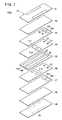
次に、上述の本実施の形態に係る積層型誘電体共振器10を用いて2段構造の積層型誘電体フィルタ100を構成した例について図5を参照しながら説明する。
【0030】
この積層型誘電体フィルタ100は、図5に示すように、複数の誘電体層(S1〜S9:図6参照)が積層、焼成一体化され、かつ、表面にアース電極12が形成された誘電体基板14を有し、誘電体基板14内には、2枚の共振電極16A及び16Bが形成されている。
【0031】
また、誘電体基板14の表面には、一方の側面に入力端子102が形成され、他方の側面に出力端子104が形成されている。なお、入力端子102とアース電極12間、並びに出力端子104とアース電極12間にはそれぞれ絶縁のための領域(誘電体基板14が露出した部分)106及び108が設けられている。
【0032】
各共振電極16A及び16Bをそれぞれ1/4波長の共振電極とした場合は、誘電体基板14の側面のうち、共振電極16A及び16Bが露出する面にアース電極12を形成して各共振電極16A及び16Bの一方の端部をアース電極12と短絡させた構造が採用される。
【0033】
そして、図6に示すように、第3の誘電体層S3の一主面には、平面的に、共振電極16A及び16Bの各開放端を含む位置にそれぞれ内層アース電極18A及び18Bが形成され、更に、共振電極16A及び16B間の結合度を調整するための結合調整電極110が形成されている。
【0034】
第5の誘電体層S5の一主面には、2枚の共振電極16A及び16Bが形成され、そのうち、入力側の共振電極16Aはリード電極112を介して入力端子102(図5参照)と接続され、出力側の共振電極16Bはリード電極114を介して出力端子104(図5参照)と接続されている。
【0035】
また、第7の誘電体層S7の一主面には、平面的に、共振電極16A及び16Bの各開放端を含む位置にそれぞれ内層アース電極20A及び20Bが形成されている。
【0036】
そして、この積層型誘電体フィルタ100は、第3及び第4の誘電体層S3及びS4のうち、各共振電極16A及び16Bの開放端部分と対応する各一方の内層アース電極18A及び18Bとの重なり部分における各一部にそれぞれ空間が設けられ、これら空間内に、第3及び第4の誘電体層S3及びS4の誘電率よりも高い誘電率を有する部材30が充填されている。
【0037】
また、第5及び第6の誘電体層S5及びS6のうち、各共振電極16A及び16Bの開放端部分と対応する各他方の内層アース電極20A及び20Bとの重なり部分における各一部にそれぞれ空間が設けられ、これら空間内に、第5及び第6の誘電体層S5及びS6の誘電率よりも高い誘電率を有する部材30が充填されている。
【0038】
この2段構造の積層型誘電体フィルタ100においては、上述した本実施の形態に係る積層型誘電体共振器10の構造を利用して構成するようにしているため、該積層型誘電体フィルタ100の製造ばらつきを抑制することができ、積層型誘電体フィルタ100の小型化並びに高い歩留まりを実現させることができる。
【0039】
次に、上述の積層型誘電体フィルタ100に関するいくつかの変形例について図7〜図9を参照しながら説明する。
【0040】
第1の変形例に係る積層型誘電体フィルタ100aは、図7に示すように、上述の積層型誘電体フィルタ100とほぼ同じ構成を有するが、第4の誘電体層S4の一主面に、入力側の共振電極16Aと入力端子102とを容量を介して結合する入力用電極116と、出力側の共振電極16Bと出力端子104とを容量を介して結合する出力用電極118とが形成されている点と、第6の誘電体層S6の一主面に結合調整電極110が形成されている点で異なる。
【0041】
第2の変形例に係る積層型誘電体フィルタ100bは、図8に示すように、上述の第1の変形例に係る積層型誘電体フィルタ100aとほぼ同じ構成を有するが、以下の点で異なる。
【0042】
即ち、各共振電極16A及び16Bと結合調整電極110間に配された第5の誘電体層S5のうち、各共振電極16A及び16Bと結合調整電極110との重なり部分における各一部にそれぞれ空間が設けられ、これら空間内に、前記第5の誘電体層S5の誘電率よりも高い誘電率を有する部材30がそれぞれ充填されて構成されている。
【0043】
第3の変形例に係る積層型誘電体フィルタ100cは、図9に示すように、上述の第1の変形例に係る積層型誘電体フィルタ100aとほぼ同じ構成を有するが、以下の点で異なる。
【0044】
即ち、各共振電極16A及び16Bと入力用電極116及び出力用電極118間に配された第4の誘電体層S4のうち、入力側の共振電極16Aと入力用電極116との重なり部分における一部と、出力側の共振電極16Bと出力用電極118との重なり部分における一部にそれぞれそれぞれ空間が設けられ、これら空間内に、前記第4の誘電体層S4の誘電率よりも高い誘電率を有する部材30がそれぞれ充填されて構成されている。
【0045】
上述の第1〜第3の変形例に係る積層型誘電体フィルタ100a〜100cにおいても、上述の本実施の形態に係る積層型誘電体フィルタ100と同様に、積層型誘電体フィルタ100a〜100cの製造ばらつきを抑制することができ、積層型誘電体フィルタ100a〜100cの小型化並びに高い歩留まりを実現させることができる。
【0046】
上述の例では、本実施の形態に係る積層型誘電体共振器10を2段構造の積層型誘電体フィルタ100、100a〜100cに適用した例を示したが、その他、図示しないが、3段構造の積層型誘電体フィルタや、4段以上の構造の積層型誘電体フィルタにも適用させることができる。
【0047】
なお、この発明に係る積層型誘電体共振器及び積層型誘電体フィルタは、上述の実施の形態に限らず、この発明の要旨を逸脱することなく、種々の構成を採り得ることはもちろんである。
【0048】
【発明の効果】
以上説明したように、本発明に係る積層型誘電体共振器及び積層型誘電体フィルタによれば、共振電極と内層アース電極の重なり状態がずれることによる特性変動を抑制することができ、積層型誘電体フィルタ等の歩留まりの向上並びに小型化を図ることができる。
【図面の簡単な説明】
【図1】本実施の形態に係る積層型誘電体共振器の構成を示す縦断面図である。
【図2】本実施の形態に係る積層型誘電体共振器の構成を示す分解斜視図である。
【図3】本実施の形態に係る積層型誘電体共振器の構成を示す平面図である。
【図4】本実施の形態に係る積層型誘電体共振器の変形例の構成を示す縦断面図である。
【図5】本実施の形態に係る積層型誘電体フィルタの構成を示す斜視図である。
【図6】本実施の形態に係る積層型誘電体フィルタの構成を示す分解斜視図である。
【図7】本実施の形態に係る積層型誘電体フィルタの第1の変形例の構成を示す分解斜視図である。
【図8】本実施の形態に係る積層型誘電体フィルタの第2の変形例の構成を示す分解斜視図である。
【図9】本実施の形態に係る積層型誘電体フィルタの第3の変形例の構成を示す分解斜視図である。
【図10】従来例に係る積層型誘電体共振器の構成を示す縦断面図である。
【符号の説明】
10…積層型誘電体共振器 12…アース電極
14…誘電体基板 16、16A、16B…共振電極
16a…開放端
18、18A、18B、20、20A、20B…内層アース電極
22、26…重なり部分 24、28…空間
30…部材
100、100a〜100c…積層型誘電体フィルタ[0001]
BACKGROUND OF THE INVENTION
The present invention relates to a laminated dielectric resonator and a laminated dielectric filter that constitute a resonance circuit in a microwave band of several hundred MHz to several GHz. The present invention relates to a multilayer dielectric resonator and a multilayer dielectric filter that can achieve downsizing and the like and high yield.
[0002]
[Prior art]
In recent years, with the diversification of wireless communication systems such as mobile phones, there has been a strong demand for miniaturization and low loss for multilayer dielectric filters.
[0003]
In order to reduce the size of the multilayer dielectric filter, the resonator (resonant electrode) must be made small.
[0004]
Therefore, conventionally, a method of adding capacitance to the open end of the resonance electrode is generally performed. In particular, in the multilayer
[0005]
[Problems to be solved by the invention]
Thus, conventionally, the internal impedance of the resonator is changed by the inner-
[0006]
In addition, in the situation where the overlapping area is small, for example, when there is a misalignment between the
[0007]
The present invention has been made in consideration of such problems, and can suppress fluctuations in characteristics due to deviation of the overlapping state of the resonance electrode and the inner layer ground electrode, thereby improving the yield of the multilayer dielectric filter and the like. It is an object of the present invention to provide a multilayer dielectric resonator and a multilayer dielectric filter that can be realized.
[0008]
[Means for Solving the Problems]
A multilayer dielectric resonator according to the present invention includes an inner layer ground electrode and a resonant electrode in a dielectric substrate formed by laminating a plurality of dielectric layers, and the resonant electrode of the dielectric substrate is included in the dielectric substrate. The dielectric constant of a part of the overlapping portion between the open end part and the inner layer ground electrode is higher than the other dielectric constants.
[0009]
Since the capacitance value between the resonance electrode and the inner layer ground electrode is governed by a part of the overlapping portion between the open end portion of the resonance electrode and the inner layer ground electrode, even if the overlapping state of the resonance electrode and the inner layer ground electrode is deviated. Since only the overlapping area in the portion having a low dielectric constant needs to be changed, the change in the capacitance value between the resonance electrode and the inner layer ground electrode is small.
[0010]
That is, in the multilayer dielectric resonator according to the present invention, it is possible to suppress the characteristic fluctuation due to the deviation of the overlapping state of the resonance electrode and the inner ground electrode, and to improve the yield of the multilayer dielectric filter and the like. Can do.
[0011]
And in the said structure, a space is provided in a part in the overlapping part of the open end part of the said resonance electrode and the said inner layer earth electrode among the said dielectric substrate, The said resonance electrode and the said inner layer earth electrode are in the said space A member having a dielectric constant higher than that of the dielectric layer disposed therebetween may be filled.
[0012]
As a result, it is possible to easily create a configuration in which the dielectric constant of a part of the dielectric substrate where the open end portion of the resonance electrode overlaps the inner ground electrode is higher than other dielectric constants. .
[0013]
In this case, one end of the member may be in contact with or close to the resonance electrode, and the other end may be in contact with or close to the inner-layer ground electrode.
[0014]
According to another aspect of the present invention, there is provided a multi-layer dielectric filter including a resonant electrode and another electrode in a dielectric substrate configured by laminating a plurality of dielectric layers, wherein the resonant electrode is included in the dielectric substrate. The dielectric constant of a part of the overlapping part between the open end part and the other electrode is higher than the other dielectric constants.
[0015]
Thereby, the characteristic fluctuation | variation by the overlapping state of a resonance electrode and another electrode shift | deviates can be suppressed, and the improvement of the yield of a laminated dielectric filter can be aimed at.
[0016]
In the above configuration, the other electrode may be an inner layer ground electrode. In addition, when a plurality of resonance electrodes are formed and a coupling adjustment electrode for adjusting the degree of coupling between the resonance electrodes is formed in the dielectric substrate, the other electrode is a coupling adjustment electrode. May be.
[0017]
A plurality of the resonance electrodes are formed, and an input electrode is formed in the dielectric substrate to couple the input-side resonance electrode and the input terminal among the plurality of resonance electrodes via a capacitor. In this case, the other electrode may be the input electrode and / or the output electrode.
[0018]
DETAILED DESCRIPTION OF THE INVENTION
Embodiments of a multilayer dielectric resonator and a multilayer dielectric filter according to the present invention will be described below with reference to FIGS.
[0019]
As shown in FIGS. 1 and 2, the multilayer
[0020]
In the example of FIG. 2, the
[0021]
When the
[0022]
In this case, the electrical length of the
[0023]
In the
[0024]
Here, the capacitance value between the
[0025]
Of these capacitance values, the capacitance value of the portion where the
[0026]
When the overlapping state of the
[0027]
As described above, in the
[0028]
In the above-described embodiment, as shown in FIG. 1, an example in which the
[0029]
Next, an example in which a
[0030]
As shown in FIG. 5, the
[0031]
Further, on the surface of the
[0032]
When each of the
[0033]
Then, as shown in FIG. 6,
[0034]
Two
[0035]
In addition, on one main surface of the seventh dielectric layer S7, inner
[0036]
The multilayer
[0037]
In addition, among the fifth and sixth dielectric layers S5 and S6, spaces are respectively provided in respective portions in the overlapping portions of the other inner
[0038]
Since the
[0039]
Next, some modified examples related to the
[0040]
As shown in FIG. 7, the
[0041]
As shown in FIG. 8, the
[0042]
That is, in the fifth dielectric layer S5 disposed between the
[0043]
As shown in FIG. 9, the
[0044]
That is, in the fourth dielectric layer S4 disposed between the
[0045]
Also in the
[0046]
In the above example, the
[0047]
The multilayer dielectric resonator and the multilayer dielectric filter according to the present invention are not limited to the above-described embodiments, and can of course have various configurations without departing from the gist of the present invention. .
[0048]
【The invention's effect】
As described above, according to the multilayer dielectric resonator and the multilayer dielectric filter according to the present invention, it is possible to suppress the characteristic variation due to the deviation of the overlapping state of the resonance electrode and the inner layer ground electrode. The yield and the size of the dielectric filter can be improved.
[Brief description of the drawings]
FIG. 1 is a longitudinal sectional view showing a configuration of a multilayer dielectric resonator according to an embodiment.
FIG. 2 is an exploded perspective view showing a configuration of a multilayer dielectric resonator according to the present embodiment.
FIG. 3 is a plan view showing a configuration of a multilayer dielectric resonator according to the present embodiment.
FIG. 4 is a longitudinal sectional view showing a configuration of a modified example of the multilayer dielectric resonator according to the present embodiment.
FIG. 5 is a perspective view showing a configuration of a multilayer dielectric filter according to the present embodiment.
FIG. 6 is an exploded perspective view showing the configuration of the multilayer dielectric filter according to the present embodiment.
FIG. 7 is an exploded perspective view showing a configuration of a first modification of the multilayer dielectric filter according to the present embodiment.
FIG. 8 is an exploded perspective view showing a configuration of a second modification of the multilayer dielectric filter according to the present embodiment.
FIG. 9 is an exploded perspective view showing a configuration of a third modification of the multilayer dielectric filter according to the present embodiment.
FIG. 10 is a longitudinal sectional view showing a configuration of a multilayer dielectric resonator according to a conventional example.
[Explanation of symbols]
DESCRIPTION OF
Claims (7)
Translated fromJapanese前記誘電体基板のうち、前記共振電極の開放端部分と前記内層アース電極との重なり部分における一部の誘電率が、その他の誘電率よりも高いことを特徴とする積層型誘電体共振器。An inner layer ground electrode and a resonant electrode in a dielectric substrate formed by laminating a plurality of dielectric layers;
A laminated dielectric resonator, wherein a dielectric constant of a part of the dielectric substrate at an overlapping portion of the open end portion of the resonant electrode and the inner layer ground electrode is higher than other dielectric constants.
前記誘電体基板のうち、前記共振電極の開放端部分と前記内層アース電極との重なり部分における一部に空間が設けられ、
前記空間内に、前記共振電極と前記内層アース電極間に配された誘電体層の誘電率よりも高い誘電率を有する部材が充填されていることを特徴とする積層型誘電体共振器。The laminated dielectric resonator according to claim 1, wherein
Of the dielectric substrate, a space is provided in a part of the overlapping portion of the open end portion of the resonance electrode and the inner layer ground electrode,
A laminated dielectric resonator, wherein the space is filled with a member having a dielectric constant higher than that of a dielectric layer disposed between the resonant electrode and the inner ground electrode.
前記部材は、一方の端部が前記共振電極に接触しあるいは近接し、他方の端部が前記内層アース電極に接触しあるいは近接していることを特徴とする積層型誘電体共振器。The laminated dielectric resonator according to claim 2, wherein
The laminated dielectric resonator according to claim 1, wherein one end of the member is in contact with or close to the resonance electrode, and the other end is in contact with or close to the inner-layer ground electrode.
前記誘電体基板のうち、前記共振電極の開放端部分と前記他の電極との重なり部分における一部の誘電率が、その他の誘電率よりも高いことを特徴とする積層型誘電体フィルタ。In a multilayer dielectric filter comprising a resonant electrode and another electrode in a dielectric substrate formed by laminating a plurality of dielectric layers,
A multilayer dielectric filter, wherein a dielectric constant of a part of the dielectric substrate at an overlapping portion between the open end portion of the resonance electrode and the other electrode is higher than other dielectric constants.
前記他の電極が内層アース電極であることを特徴とする積層型誘電体フィルタ。The laminated dielectric filter according to claim 4, wherein
2. The multilayer dielectric filter according to claim 1, wherein the other electrode is an inner layer ground electrode.
前記共振電極が複数形成され、前記誘電体基板内に前記各共振電極間の結合度を調整するための結合調整電極が形成されている場合に、
前記他の電極が結合調整電極であることを特徴とする積層型誘電体フィルタ。The laminated dielectric filter according to claim 4, wherein
When a plurality of the resonance electrodes are formed and a coupling adjustment electrode for adjusting the degree of coupling between the resonance electrodes is formed in the dielectric substrate,
The multilayer dielectric filter, wherein the other electrode is a coupling adjustment electrode.
前記共振電極が複数形成され、前記誘電体基板内に、前記複数の共振電極のうち、入力側の共振電極と入力端子とを容量を介して結合する入力用電極が形成され、出力側の共振電極と出力端子とを容量を介して結合する出力用電極が形成されている場合に、
前記他の電極が前記入力用電極及び/又は出力用電極であることを特徴とする積層型誘電体フィルタ。The laminated dielectric filter according to claim 4, wherein
A plurality of the resonance electrodes are formed, and an input electrode that couples the resonance electrode on the input side and the input terminal among the plurality of resonance electrodes via a capacitor is formed in the dielectric substrate, and the resonance on the output side is formed. When an output electrode that couples the electrode and the output terminal via a capacitor is formed,
The multilayer dielectric filter, wherein the other electrode is the input electrode and / or the output electrode.
Priority Applications (4)
| Application Number | Priority Date | Filing Date | Title |
|---|---|---|---|
| JP2001060643AJP4401586B2 (en) | 2001-03-05 | 2001-03-05 | Multilayer dielectric resonator and multilayer dielectric filter |
| US10/085,833US6765459B2 (en) | 2001-03-05 | 2002-02-28 | Laminated dielectric resonator and laminated dielectric filter |
| DE10209543ADE10209543B4 (en) | 2001-03-05 | 2002-03-04 | Layered dielectric resonator and layered dielectric filter |
| CNB02106959XACN1174516C (en) | 2001-03-05 | 2002-03-05 | Multilayer dielectric resonator and multilayer dielectric filter |
Applications Claiming Priority (1)
| Application Number | Priority Date | Filing Date | Title |
|---|---|---|---|
| JP2001060643AJP4401586B2 (en) | 2001-03-05 | 2001-03-05 | Multilayer dielectric resonator and multilayer dielectric filter |
Publications (2)
| Publication Number | Publication Date |
|---|---|
| JP2002261518A JP2002261518A (en) | 2002-09-13 |
| JP4401586B2true JP4401586B2 (en) | 2010-01-20 |
Family
ID=18920034
Family Applications (1)
| Application Number | Title | Priority Date | Filing Date |
|---|---|---|---|
| JP2001060643AExpired - LifetimeJP4401586B2 (en) | 2001-03-05 | 2001-03-05 | Multilayer dielectric resonator and multilayer dielectric filter |
Country Status (4)
| Country | Link |
|---|---|
| US (1) | US6765459B2 (en) |
| JP (1) | JP4401586B2 (en) |
| CN (1) | CN1174516C (en) |
| DE (1) | DE10209543B4 (en) |
Cited By (1)
| Publication number | Priority date | Publication date | Assignee | Title |
|---|---|---|---|---|
| KR101430684B1 (en)* | 2013-04-12 | 2014-08-14 | 주식회사 이너트론 | Resonance device and filter using the same |
Families Citing this family (6)
| Publication number | Priority date | Publication date | Assignee | Title |
|---|---|---|---|---|
| CN1319208C (en)* | 2001-03-02 | 2007-05-30 | 松下电器产业株式会社 | Dielectric filter, antenna transceiving conversion device and communication device using filter |
| AU2005280153B2 (en)* | 2004-08-26 | 2011-03-31 | Noveon, Inc. | Coating compositions having improved stability |
| JP4580795B2 (en)* | 2005-03-23 | 2010-11-17 | 双信電機株式会社 | Unbalanced to balanced converter |
| KR101439420B1 (en) | 2013-11-11 | 2014-09-11 | 주식회사 이너트론 | Resonator and filter having the same |
| KR101598980B1 (en)* | 2014-05-07 | 2016-03-02 | 주식회사 이너트론 | Resonacne device and filter including the same |
| KR101591878B1 (en)* | 2014-05-20 | 2016-02-04 | 주식회사 이너트론 | Resonacne device and filter including the same |
Family Cites Families (7)
| Publication number | Priority date | Publication date | Assignee | Title |
|---|---|---|---|---|
| US5293140A (en)* | 1991-01-02 | 1994-03-08 | Motorola, Inc. | Transmission line structure |
| US5374909A (en)* | 1992-02-28 | 1994-12-20 | Ngk Insulators, Ltd. | Stripline filter having internal ground electrodes |
| JP3144744B2 (en)* | 1993-11-02 | 2001-03-12 | 日本碍子株式会社 | Multilayer dielectric filter |
| JPH10209714A (en) | 1996-11-19 | 1998-08-07 | Sharp Corp | Voltage-controlled passband variable filter and high-frequency circuit module using the same |
| JPH10209707A (en)* | 1997-01-21 | 1998-08-07 | Matsushita Electric Ind Co Ltd | Multilayer filter and multilayer module |
| JPH11284406A (en)* | 1998-03-31 | 1999-10-15 | Ngk Insulators Ltd | Stacked dielectric filter |
| JPH11355008A (en)* | 1998-06-08 | 1999-12-24 | Ngk Insulators Ltd | Laminated dielectric filter |
- 2001
- 2001-03-05JPJP2001060643Apatent/JP4401586B2/ennot_activeExpired - Lifetime
- 2002
- 2002-02-28USUS10/085,833patent/US6765459B2/ennot_activeExpired - Lifetime
- 2002-03-04DEDE10209543Apatent/DE10209543B4/ennot_activeExpired - Fee Related
- 2002-03-05CNCNB02106959XApatent/CN1174516C/ennot_activeExpired - Fee Related
Cited By (2)
| Publication number | Priority date | Publication date | Assignee | Title |
|---|---|---|---|---|
| KR101430684B1 (en)* | 2013-04-12 | 2014-08-14 | 주식회사 이너트론 | Resonance device and filter using the same |
| US9520634B2 (en) | 2013-04-12 | 2016-12-13 | Innertron, Inc. | Resonance device |
Also Published As
| Publication number | Publication date |
|---|---|
| DE10209543A1 (en) | 2003-05-15 |
| US20020121946A1 (en) | 2002-09-05 |
| CN1374755A (en) | 2002-10-16 |
| DE10209543B4 (en) | 2004-07-15 |
| CN1174516C (en) | 2004-11-03 |
| JP2002261518A (en) | 2002-09-13 |
| US6765459B2 (en) | 2004-07-20 |
Similar Documents
| Publication | Publication Date | Title |
|---|---|---|
| US6828881B2 (en) | Stacked dielectric filter | |
| JP4579198B2 (en) | Multilayer bandpass filter | |
| US6351239B1 (en) | Electronic device in which integrated antenna and filter both have balanced terminals | |
| US7432786B2 (en) | High frequency filter | |
| US20120098622A1 (en) | Multilayer filter | |
| US6417745B1 (en) | LC filter with a coupling capacitor formed by shared first and second capacitor patterns | |
| US8120446B2 (en) | Electronic component | |
| JP4401586B2 (en) | Multilayer dielectric resonator and multilayer dielectric filter | |
| US8456256B2 (en) | Electronic component and passive component | |
| US20060103488A1 (en) | Duplexer, and laminate-type high-frequency device and communication equipment using the same | |
| US7463120B2 (en) | High frequency filter | |
| JP3955212B2 (en) | Multilayer dielectric filter | |
| JP2003218604A (en) | Laminated dielectric resonator and laminated dielectric filter | |
| JP4019097B2 (en) | Multilayer dielectric filter | |
| JP3949296B2 (en) | Antenna device | |
| JP4291488B2 (en) | Multilayer dielectric resonator | |
| JP4279695B2 (en) | Antenna device | |
| JP2004320556A (en) | Passive components | |
| JP4185805B2 (en) | Multilayer dielectric filter | |
| JP3295333B2 (en) | Dielectric filter | |
| JP3098415B2 (en) | Multilayer dielectric filter | |
| JPH10190311A (en) | Dielectric filter | |
| JPH10303602A (en) | Lamination band pass filter | |
| JP2003115709A (en) | Laminated dielectric resonator and laminated dielectric filter | |
| JP2002252509A (en) | Laminated dielectric resonator and laminated dielectric filter |
Legal Events
| Date | Code | Title | Description |
|---|---|---|---|
| A621 | Written request for application examination | Free format text:JAPANESE INTERMEDIATE CODE: A621 Effective date:20080303 | |
| A977 | Report on retrieval | Free format text:JAPANESE INTERMEDIATE CODE: A971007 Effective date:20090210 | |
| TRDD | Decision of grant or rejection written | ||
| A01 | Written decision to grant a patent or to grant a registration (utility model) | Free format text:JAPANESE INTERMEDIATE CODE: A01 Effective date:20091013 | |
| A01 | Written decision to grant a patent or to grant a registration (utility model) | Free format text:JAPANESE INTERMEDIATE CODE: A01 | |
| A61 | First payment of annual fees (during grant procedure) | Free format text:JAPANESE INTERMEDIATE CODE: A61 Effective date:20091028 | |
| R150 | Certificate of patent or registration of utility model | Ref document number:4401586 Country of ref document:JP Free format text:JAPANESE INTERMEDIATE CODE: R150 Free format text:JAPANESE INTERMEDIATE CODE: R150 | |
| FPAY | Renewal fee payment (event date is renewal date of database) | Free format text:PAYMENT UNTIL: 20121106 Year of fee payment:3 | |
| FPAY | Renewal fee payment (event date is renewal date of database) | Free format text:PAYMENT UNTIL: 20131106 Year of fee payment:4 | |
| R250 | Receipt of annual fees | Free format text:JAPANESE INTERMEDIATE CODE: R250 | |
| R250 | Receipt of annual fees | Free format text:JAPANESE INTERMEDIATE CODE: R250 | |
| R250 | Receipt of annual fees | Free format text:JAPANESE INTERMEDIATE CODE: R250 | |
| R250 | Receipt of annual fees | Free format text:JAPANESE INTERMEDIATE CODE: R250 | |
| R250 | Receipt of annual fees | Free format text:JAPANESE INTERMEDIATE CODE: R250 | |
| R250 | Receipt of annual fees | Free format text:JAPANESE INTERMEDIATE CODE: R250 | |
| R250 | Receipt of annual fees | Free format text:JAPANESE INTERMEDIATE CODE: R250 | |
| R250 | Receipt of annual fees | Free format text:JAPANESE INTERMEDIATE CODE: R250 | |
| R250 | Receipt of annual fees | Free format text:JAPANESE INTERMEDIATE CODE: R250 | |
| EXPY | Cancellation because of completion of term |