JP4397567B2 - Optical AND gate and waveform shaping device - Google Patents
Optical AND gate and waveform shaping deviceDownload PDFInfo
- Publication number
- JP4397567B2 JP4397567B2JP2002197109AJP2002197109AJP4397567B2JP 4397567 B2JP4397567 B2JP 4397567B2JP 2002197109 AJP2002197109 AJP 2002197109AJP 2002197109 AJP2002197109 AJP 2002197109AJP 4397567 B2JP4397567 B2JP 4397567B2
- Authority
- JP
- Japan
- Prior art keywords
- optical
- light
- gate
- wavelength
- signal
- Prior art date
- Legal status (The legal status is an assumption and is not a legal conclusion. Google has not performed a legal analysis and makes no representation as to the accuracy of the status listed.)
- Expired - Fee Related
Links
Images


Classifications
- H—ELECTRICITY
- H04—ELECTRIC COMMUNICATION TECHNIQUE
- H04B—TRANSMISSION
- H04B10/00—Transmission systems employing electromagnetic waves other than radio-waves, e.g. infrared, visible or ultraviolet light, or employing corpuscular radiation, e.g. quantum communication
- H04B10/29—Repeaters
- H04B10/291—Repeaters in which processing or amplification is carried out without conversion of the main signal from optical form
- H04B10/299—Signal waveform processing, e.g. reshaping or retiming
- G—PHYSICS
- G02—OPTICS
- G02F—OPTICAL DEVICES OR ARRANGEMENTS FOR THE CONTROL OF LIGHT BY MODIFICATION OF THE OPTICAL PROPERTIES OF THE MEDIA OF THE ELEMENTS INVOLVED THEREIN; NON-LINEAR OPTICS; FREQUENCY-CHANGING OF LIGHT; OPTICAL LOGIC ELEMENTS; OPTICAL ANALOGUE/DIGITAL CONVERTERS
- G02F1/00—Devices or arrangements for the control of the intensity, colour, phase, polarisation or direction of light arriving from an independent light source, e.g. switching, gating or modulating; Non-linear optics
- G02F1/35—Non-linear optics
- G02F1/3515—All-optical modulation, gating, switching, e.g. control of a light beam by another light beam
- G—PHYSICS
- G02—OPTICS
- G02F—OPTICAL DEVICES OR ARRANGEMENTS FOR THE CONTROL OF LIGHT BY MODIFICATION OF THE OPTICAL PROPERTIES OF THE MEDIA OF THE ELEMENTS INVOLVED THEREIN; NON-LINEAR OPTICS; FREQUENCY-CHANGING OF LIGHT; OPTICAL LOGIC ELEMENTS; OPTICAL ANALOGUE/DIGITAL CONVERTERS
- G02F2/00—Demodulating light; Transferring the modulation of modulated light; Frequency-changing of light
- G02F2/004—Transferring the modulation of modulated light, i.e. transferring the information from one optical carrier of a first wavelength to a second optical carrier of a second wavelength, e.g. all-optical wavelength converter
- G—PHYSICS
- G02—OPTICS
- G02F—OPTICAL DEVICES OR ARRANGEMENTS FOR THE CONTROL OF LIGHT BY MODIFICATION OF THE OPTICAL PROPERTIES OF THE MEDIA OF THE ELEMENTS INVOLVED THEREIN; NON-LINEAR OPTICS; FREQUENCY-CHANGING OF LIGHT; OPTICAL LOGIC ELEMENTS; OPTICAL ANALOGUE/DIGITAL CONVERTERS
- G02F3/00—Optical logic elements; Optical bistable devices
Landscapes
- Physics & Mathematics (AREA)
- Nonlinear Science (AREA)
- General Physics & Mathematics (AREA)
- Optics & Photonics (AREA)
- Electromagnetism (AREA)
- Engineering & Computer Science (AREA)
- Computer Networks & Wireless Communication (AREA)
- Signal Processing (AREA)
- Optical Modulation, Optical Deflection, Nonlinear Optics, Optical Demodulation, Optical Logic Elements (AREA)
Description
Translated fromJapanese【0001】
【発明の属する技術分野】
本発明は、信号光を波形整形するための方法及び装置に関する発明で、特に光信号と光クロックにより光信号再生を行う光ANDゲートに関する発明である
【0002】
【従来の技術】
近年実用化されている光ファイバ通信システムにおいては、伝送路損失や分岐損失等による信号パワーの低下を、エルビウムドープファイバ増幅器(EDFA)等の光増幅器を用いて補償している。光増幅器はアナログ増幅器であり、信号を線形増幅するものである。この種の光増幅器においては、増幅に伴って発生する自然放出光(ASE)雑音の付加により信号対雑音比(S/N比)が低下するので、中継数ひいては伝送距離に限界が生じる。また、光ファイバの持つ波長分散やファイバ内の非線形光学効果による波形劣化も伝送限界を与える要因である。こうした限界を打破するためには、信号をデジタル的に処理する再生中継器が必要であり、その実現が望まれている。特に、全ての処理を光レベルにおいて行う全光再生中継器は、信号のビットレートやパルス形状等に依存しないトランスペアレントな動作を実現する上で重要である。
【0003】
全光再生中継器に必要な機能は、振幅再生又はリアンプリフィケーション(Reamplification)と、波形整形又はリシェイピング(Reshaping)と、タイミング再生又はリタイミング(Retiming)とである。これらの機能は3R機能と称され、特に前二者は2R機能と称される。
【0004】
光レベルで光信号再生を行う装置として、光信号を一旦電気信号に変換し、電気段で信号再生を行った後、その再生電気信号を用いてレーザー光を変調して光信号に変換する光・電気・光(O・E・O)変換型、及び電気信号への変換なしに光レベルで信号再生する全光型のものがある。このうちO・E・O型は既に10Gb/s程度までは実用化されているが、性能がエレクトロニクスの動作速度に依存するため、40Gb/s以上での動作は難しい。一方、現状では全光型は実用化レベルのものはないが、いくつかの方式が提案されている。
【0005】
全光型の代表的なものとしてマッハ・ツェンダ干渉器(MZI)型光ゲートがある。この光ゲートは、位相シフトを与えるための第1及び第2の非線形光学媒質を含むMZIを例えば光導波路基板上に集積化して構成される。連続波(CW)光あるいは光パルスとしてのプロープ光が等分配されて第1及び第2の非線形光学媒質に供給される。このとき、等分配されたプローブ光の干渉により出力光が得られないように干渉計の光路長が設定されている。
【0006】
第1及び第2の非線形光学媒質の一方には更に信号光が供給される。信号光及びプローブ光のパワーを適切に設定することによって、信号光に同期する変換光信号がこの光ゲートから出力される。変換光信号はプローブ光と同じ波長を有している。
【0007】
第1及び第2の非線形光学媒質の各々として半導体光アンプ(SOA)を用いることが提案されている。例えば、波長1.5μm帯において、両端面を無反射化処理したInGaAs−SOAを各非線形光学媒質として用い、これらをInP/GaInAsP基板上に集積化したものが作製されている。特に動作速度を向上させるために、超高速非線形干渉器(UNI)と呼ばれるタイプが提案されている。これは、干渉器の二つの光路を通過する光パルスのタイミングを僅かにずらし、半導体媒質のキャリア効果に起因する動作速度限界を改善したものである。
【0008】
従来知られている他の波形整形装置として、非線形光ループミラー(NOLM)がある。NOLMは、方向性結合される第1及び第2の光路を含む第1の光カプラと、第1及び第2の光路を接続するループ光路と、ループ光路に方向性結合される第3の光路を含む第2の光カプラとを備えている。
【0009】
ループ光路の一部または全体を非線形光学媒質から構成するとともに、第1及び第3の光路にそれぞれプローブ光及び信号光を供給することによって、変換光信号が第2の光路から出力される。
【0010】
NOLMにおける非線形光学媒質としては光ファイバが一般的である。特に、非線形光学媒質としてSOAを用いたNOLMはSLALOM(Semiconductor Laser Amplifier in a Loop Mirror)と称される。
【0011】
【発明が解決しようとする課題】
波形整形装置と光クロック再生装置を組み合わせることにより、3R機能を提供することができる。この場合、一般的には、3R再生されるべき信号光と再生光クロックパルスとが光ANDゲートに入力され、AND動作により信号光の持つデータが再生光クロックに転写される。波形整形は、光ANDゲートに入力する前若しくは後に波形整形装置を用いて行うか、あるいは光ANDゲートに波形整形機能を併せ持たせることによって可能である。
【0012】
光3R機能を提供するための波形整形装置においては、光ANDゲートに入力する信号光と再生光クロックパルスの時間軸上の相対的な位置ずれに応じて、十分な3R機能を得ることができない場合があるという問題がある。このような相対的な位置ずれの原因としては、光ANDゲート内での信号光と再生光クロックパルスの間のウオークオフや各光パルスの時間的な安定度、ジッター等が考えられる。
【0013】
これまでに提案されている3R機能としては、例えば、前述のMZI型光ゲートスイッチによるものがある。我々は、先に2R機能及び/又は3R機能を提供するための波形整形装置を提案している(特願平11−293189号)。この装置においては、2つのNOLMを組み合わせることによって、波形整形或いは光ゲートの機能を得る場合における波長変換の自由度を大きくしている。しかしながら、上記に述べたNOLM等の光ANDゲートや光再生中継器で波長変換を行うためには、入力するプローブ光を最終的に得ようとする波長で発信させることが必要であり、プローブ光を発信させるレーザで波長変換できる波長が決まってしまう問題が有る。
【0014】
よって、本発明の目的は、光3R機能を行う際の波長変換を容易に任意の波長にする方法及び装置を提供することである。本発明の更に他の目的は以下の説明から明らかになる。
【0015】
【課題を解決するための手段】
第1の発明の光ANDゲートは、第1の波長を有する信号光及び前記第1の波長と異なる第2の波長を有するプローブ光が入力され前記プローブ光を前記信号光で相互位相変調することでスペクトル拡大した光を出力する非線形光学媒質と、前記非線形光学媒質により前記スペクトル拡大した光から前記信号光の変調成分が含まれ且つ前記スペクトル拡大された光の帯域幅よりも狭い帯域を有する光を抽出する光フィルタとを備え、前記非線形光学媒質に入力される前記信号光のパワーは前記プローブ光のパワーの10倍から100倍のパワーであり、前記非線形光学媒質は光ファイバから成り、前記プローブ光の波長は前記光ファイバの異常分散領域に位置し、記信号光の波長は、前記光ファイバの異常分散領域であり、前記信号光と前記プローブ光のウオークオフを小さく抑える。
【0016】
この第1の発明の構成では、光ANDゲート内の非線形光学媒質内でプローブ光がスペクトルを拡大し、そのスペクトルを拡大した光から新たに信号成分を抽出しているので、プローブ光の波長を変えることなく光ANDゲートに於いて任意の波長を出力することができる。従って、波長変換の自由度を上げることができる。
【0017】
さらに、スペクトル拡大により出力レベルの変動が抑圧されるので、信号光の振幅雑音を抑圧することができる。
【0018】
従って、超高速信号に対しても、光3R処理、波長変換処理、光デマルチプレクシング処理といった光信号処理を安定に行うことができるようになる。
【0019】
第2の発明の波形整形装置は、第1の発明の光ANDゲートと、該光ANDゲートの出力を自己位相変調によりスペクトル拡大した光を出力する第2の非線形光学媒質と、前記第2の非線形光学媒質により前記スペクトル拡大した光から前記光ANDゲートの出力の信号成分が含まれ且つ前記スペクトル拡大された光の帯域幅よりも狭い帯域を有する光を抽出する第2の光フィルタとを設ける。
【0020】
第2の発明の構成によると、第1の発明の光ANDゲートで任意の波長に変換された波長をさらに第2の非線形光学媒質で自己位相変調をかけ、出力光のスペクトルを拡大して、そこから新たに信号成分を抽出するようにしているので、波長変換の自由度をさらに大きくすることができる。この構成にすることにより光ANDゲートに入力する信号光と同じ波長にも変換することができ、光ANDゲートに入力する信号光波長で、振幅雑音を低減した信号光を得ることができる。さらに、自己位相変調による出力光のスペクトルを拡大により出力レベルの変動抑圧されるので、光ANDゲート単体よりも信号光の振幅雑音を抑圧することができる。
【0021】
第3の発明の波形整形装置は、第1の発明の光ANDゲートと、該光ANDゲートの出力光と前記光ANDゲートの出力光波長と異なる波長の第2プローブ光を入力し、前記第2プローブ光を前記光ANDゲートの出力光で相互位相変調することでスペクトル拡大した光を出力する第2の非線形光学媒質と、前記第2の非線形光学媒質により前記スペクトル拡大した光から前記光ANDゲートの出力の信号成分が含まれ且つ前記スペクトル拡大された光の帯域幅よりも狭い帯域を有する光を抽出する第2の光フィルタとを設ける。
【0022】
第3の発明の構成によると、光ANDゲートの出力光をプローブ光により相互位相変調するので、プローブ光の波長を変えることなく光ANDゲートに於いて任意の波長を出力することができるため、波長変換の自由度を上げることができる。この構成にすることにより光ANDゲートに入力する信号光と同じ波長にも変換することができ、光ANDゲートに入力する信号光波長で、振幅雑音を低減した信号光を得ることができる。さらに、相互位相変調で光ANDゲートの出力光とプローブ光がスペクトル拡大することにより出力レベルの変動抑圧されるので、光ANDゲート単体よりも信号光の振幅雑音を抑圧することができる。
【0025】
第4,5の発明の光ANDゲート及び波形整形装置は、第1の発明、第2の発明、第3の発明の光ANDゲートにおいて、伝送路からの信号光のパルス幅を拡大した光と該伝送路からの光信号より抽出した光クロックを入力する構成とする。第4,5の発明によれば光ANDゲート及び波形整形装置の信号光及びクロックパルスのジッターや時間的な不安定性に起因して光ANDゲート内で発生する振幅雑音等を抑制することができる。
【0026】
【発明の実施の形態】
以下、添付図面を参照して、本発明の望ましい実施形態を詳細に説明する。全図を通して実質的に同一又は類似の部分には同一の符号が付されている。
【0027】
本発明の望ましい実施形態では、光ANDゲートにおいて、プローブ光を信号光により相互位相変調(XPM)し、これによりプローブ光のスペクトルを拡大し、そのスペクトルの中からスペクトル中心波長と異なる成分を光帯域通過フィルタにより抽出することにより、波長変換された信号成分を取り出す。
【0028】
そして、例えば、波長変換された信号成分を更に波長変換し、もとの信号光の波長と一致させたり、任意の波長に変換したりさせる。この波長変換では、スペクトルを自己位相変調(SPM)により拡大し、そのスペクトルの中心波長と異なる成分を光帯域通過フィルタにより抽出する方法等を用いることができる。この方法により、振幅雑音抑圧のための波形整形を信号光に対して施すことができる。
【0029】
また、波長変換の手法としてはスペクトルを相互位相変調(XPM)により拡大する方法も用いることができる。
【0030】
XPMを行う光ANDゲートや波長変換器のプローブ光としては、連続波光(CW光)あるいは光パルス列を用いることができ、特に、光パルス列としても元の信号光から再生した光クロックパルスを用いることもできる。
【0031】
本発明によると、信号光の振幅雑音やジッター等を抑圧することができ、超高速信号に対しても、光3R装置、波長変換装置、光デマルチプレクサといった光信号処理装置の提供が可能になる。
【0032】
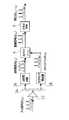
図1を参照すると、前述の本発明の望ましい実施形態の基本構成が示されている。
【0033】
波長λSの入力信号光はEDFA(エルビウムドープファイバ増幅器)等の光増幅器2により適切なパワーに増幅されて、光ANDゲート4に供給される。また、適切なパワーで波長λPのプローブ光が光ANDゲート4に供給される。
【0034】
光ANDゲート4における非線形光学効果による論理積により得られた波長λS´の変換光が光ANDゲート4から出力され、この変換光は波長変換器6に入力される。
【0035】
波長変換器6は、入力した変換光の波長をλCに変換して再生光として出力する。ここで、再生光の波長λCは例えば入力信号光の波長λSに等しく設定することができる。
【0036】
任意の波長に波長変換を行う光ANDゲート4は、XPMによるスペクトル拡大を用いて実現することができる。
【0037】
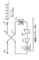
図2は本発明の光ANDゲート4による装置の実施形態を示すブロック図である。
【0038】
光ANDゲート4は、入力信号光とプローブ光を加え合わせるための光カプラ8と、光カプラ8からの信号光及びプローブ光が入力する非線形光学媒質としての光ファイバ10と、光ファイバ10から出力された光が供給される光帯域通過フィルタ(BPF)12とを含む。
【0039】
非線形光学媒質に光パルスが入力すると、XPMによるチャーピングが発生して、プローブ光のスペクトルが拡大する。
【0040】
図2の上部に示されているように、波長λSの入力信号光と波長λPのプローブ光が光カプラ8により合波され光ファイバ10に入力する。
【0041】
プローブ光としては、連続波光(CW光)あるいは図2で示した様な光パルス列を用いることができ、特に、光パルス列として元の信号光から再生した光クロックパルスを用いることもできる。
【0042】
光ファイバ10内ではプローブ光が中心波長λPを中心として拡大されていることがわかる。
【0043】
そして、この拡大されたスペクトルの範囲内で波長λPと異なるλS´を中心波長とする通過帯域を有する光帯域通過フィルタ12により信号成分を抽出する。通過帯域は、拡大されたスペクトルよりも狭く設定されている。
【0044】
このとき、通常は一定であるはずの信号光の振幅が伝送等による歪のためにパルス毎に異なる場合でも(振幅揺らぎあるいは振幅雑音)、チャーピングが発生する範囲ではスペクトルが一定となるため、振幅揺らぎを抑圧することが可能である。即ち、波形整形の機能が得られているのである。
【0045】
更に詳しく説明すると、光帯域通過フィルタ12ではチャーピングの小さな成分及びチャーピングの必要以上に大きな成分が除去される。チャーピングの小さな成分には、主にオフパワー(0符合)成分の零点からの変動分(例えばGVDによる波形劣化)やパルスのピーク付近のスロープの小さな成分が含まれる。
【0046】
一方、チャーピングが必要以上に大きな成分には主にオンパワー(1符号)成分のピーク付近のスロープの大きな揺らぎ成分が含まれる。これらの成分は光信号対雑音比(OSNR)を決定付けるものであるので、この部分を光帯域通過フィルタ12により除去することにより、これらの成分のパワー変動、消光比劣化、雑音累積等によるOSNRの低下を改善することができる。従って、本発明により、OSNRの改善を伴う波長変換が可能になる。
【0047】
光帯域通過フィルタ12の通過帯域の中心波長λS´は、雑音を含むチャープの小さい成分とチャープが必要以上に大きな成分が出力信号パルスに含まれないように、プローブ光の中心波長λPから十分に離しておくことが望ましい。
【0048】
振幅揺らぎを持つ信号光を入力した場合、プローブ光の波長λpの位置は他の波長より振幅雑音が大きい。従って、その部分を外す必要がある。また、スペクトル拡大した光の最も短波長側と長波長側のエッジ部分にもノイズが多く存在するので避けるのが望ましい。
【0049】
光帯域通過フィルタ12の通過帯域の幅及び形状は、必要とされるパルスの幅及び形状に応じて適宜設定しておくことが望ましい。 基本的には、入力信号が伝送路に入力され劣化する前のスペクトル幅とほぼ等しく設定されるのが望ましい。
【0050】
尚、非線形光学媒質用の材料としては光ファイバ(通常の単一モード光ファイバも含む)が利用できる。
【0051】
特に、高非線形ファイバやフォトニック結晶ファイバ(Holey Fiber)が適している。
【0052】
これらの光ファイバは、通常の単一モード光ファイバが3次非線型係数γが2(W-1Km-1)(1Kmのファイバに1Wの光パワーを入力した時に位相が2ラジアン回る)程度であるのに対して、高非線形ファイバでは3次非線型係数γが約20(W-1Km-1)、フォトニック結晶ファイバでは3次非線型係数γが約100(W-1Km-1)程度のものが開発されている。
【0053】
また、XPMによる位相シフト量Δφは
Δφ=γPL (γは3次非線型係数、Pは光パワー、Lは非線形媒質の長さ)
である。
【0054】
従って、入力パワーを強くしてもXPMやSPMは強く発生するので、光増幅器2及び14により光ANDゲートに入力する光を充分大きくすることも有効な手段である。
【0055】
この時、入力信号光波長λsのパワーPλsはプローブ光波長λpのパワーPλpに対して、10倍から100倍に設定しておくことにより、効率よくプローブ光波長λp側を相互位相変調することができる。
【0056】
また、3次非線型係数γは
γ=2πn2/λAeff (n2は非線形屈折率、Aeffは実行断面積、λは波長)と表されるので、非線形光学媒質内で光が伝播する領域の面積である実行断面積を小さくすることで、実質的に入力パワーを強くした時と同じ効果が得られる。図2では光フィルタは固定のバンドパスフィルタで説明しているが、可変の光フィルタを用いて信号光を切り出しても良い。
【0057】
振幅雑音を少なくし任意の波長に変換するだけの場合は図2の構成だけでも充分であるが、入力信号光の波長を基の波長に戻したり、XPMにより拡大されたスペクトルの範囲より外に波長変換を設定したりしたい場合は、図1に示すように、光ANDゲート4の出力をさらに波長変換器6で変換すると良い。
【0058】
波長変換器6の具体的構成を図3と図8を用いて説明する。
【0059】
図3では波長λS´の変換光を光増幅器16により適切なパワーに増幅し、それを非線形光学媒質としての光ファイバ18に入力する。すると、自己位相変調(SPM)によって変換光のスペクトルが波長λS´を中心として拡大されるので、元の波長λSを通過中心波長とする光から光帯域通過フィルタ20により信号成分を抽出して再生光として出力するものである。
【0060】
この波長変換によって、光ANDゲート4(図1参照)によっても残留する振幅揺らぎを更に抑圧することができる。振幅揺らぎが抑圧される原理は、前述のXPMにおけるのと同様であるので、その説明を省略する。
【0061】
図8に、波長変換器6の別な構成を示す。
【0062】
波長変換器6は光ファイバ101と光増幅器161,141と光フィルタ201より構成される。
【0063】
光ゲート回路4からの変換光λs'とプローブ光として波長λp'の連続発光するCW光を第二の光ファイバ101に入力する。
【0064】
CW光λp'は光ファイバ101内で変換光λs’によりXPMによりスペクトルを広げられるとともに、変換光λs'と同じ変調成分を有する信号光に変換される。
【0065】
このXPMにより波長λp'を中心としてスペクトルが広がった信号光の波長λsを光フィルタ201により切り出すことで、再生光の波長をλsとすることができる。
【0066】
この時の光フィルタ201選択波長の位置を波長λp'の中心とするスペクトルが広がった信号光の任意の位置とすることで、光信号再生装置に入力される信号光波長λsに波長を戻すこともできるし、他の波長にも変換することができる。
【0067】
このような波長変換によって、光ANDゲート4による変換によっても残留する振幅ゆらぎをさらに抑えることができる。
【0068】
光ファイバ101でXPMを有効に発生させるため、必要に応じて、光ファイバ101に入力される変換光λs'は光増幅器161で増幅される。
【0069】
また、再生光λsの光S/N比はCW光λp'のパワーレベルに比例するので、光ファイバ101に入力するCW光λp'は光増幅器141で増幅される。
【0070】
各光増幅器の出力パワーの関係は図2の関係と同様で、変換光λs'のパワーを大きくするとXPMを行うのに効果的である。
【0071】
図3及び図8の構成を波長変換器6として用いると、スペクトルの拡大とそれに伴う振幅雑音の抑圧が行われるので、光ANDゲート4としては図2のようなXPMを用いた光Kerrスィッチの他にNOLM,UNI(Ultra−fast Nonlinear Interferometer)、更には四光波混合や差周波生成等の非線形光学効果を用いた方法等も採用可能である。
【0072】
また、光-電気-光変換等の信号出力に対して、図3や図8の構成を組み合わせて使用することができる。
【0073】
このように、例えば図1に示される実施形態では、光ANDゲート4及び波長変換器6で、単独またはその組み合わせによりスペクトルを拡大して波長選択することで、光3Rをはじめとする各種光スイッチングが可能となる。
【0074】
さらに、図2、図3、図8に述べた非線形光学媒質として用いる光ファイバはその分散が重要である。
【0075】
まず、スペクトルの拡大を有効に行わせる観点からは、波長λpの分散は小さくしかも異常分散領域に設定するほうがよい。しかし、分散が小さすぎて零に近い場合には、光増幅器等から発生するASE(自然放出光)雑音が非線形的に増幅され(変調不安定)、S/Nが劣化する。高いS/Nを確保する上では正常分散領域で光ファイバを用いるのが有効であるが、この場合にはスペクトルの拡大は制限される。
【0076】
従って、大きな波長シフトを優先する場合には異常分散領域を選択し、波長シフトは小さくとも高いS/Nを優先する場合には正常分散領域を選択するというように、システム毎に最適な分散を設定するのがよい。
【0077】
一方、プローブ光として光パルス列を用いる場合には、XPMを発生させる光ファイバ10(図2参照)の中で信号光とプローブ光のウオークオフ(Walk−off)を小さく抑えるのが望ましい。
【0078】
この観点からは分散は小さい方が良い。例えば、信号光の波長及びプローブ光の波長を共に正常分散領域あるいは異常分散領域に配置する方法、ウオークオフを最も小さくするために零分散を挟んで両波長を対称に配置する方法、更には分散フラットファイバを使用する方法、分散補償を用いる方法等がある。
【0079】
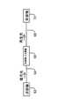
図4は本発明による装置の他の実施形態を示すブロック図である。この装置は、光増幅器22、光カプラ24、波形整形器26、光クロック再生器28、光ANDゲート4、及び波長変換器6を備えている。
【0080】
光ANDゲート4及び波長変換器6は図1に示されるものを用いることができる。
【0081】
波形整形されるべき波長λsの光信号(入力信号光)は、光増幅器22によって増幅された後に光カプラ24で第1及び第2の信号光に分岐される。
【0082】
第1の信号光は波形整形器26に供給され、第1の信号光のパルス幅を拡大して得られた波形整形光(波長λs)が波形整形器26から出力される。
【0083】
第2の信号光は光クロック再生器28に供給され、第2の信号光に基いて波長λPのプローブ光としてのクロックパルスが生成される。
【0084】
波形整形光及びクロックパルスは光ANDゲート4に供給され、波形整形光及びクロックパルスが共に存在する時間に同期して波長λs′の変換光信号(変換信号光)が光ANDゲート4から出力される。
【0085】
変換信号光は波長変換器6でその波長をλC(望ましくはλC=λS)に変換されて再生光が得られる。
【0086】
光クロック再生器28は、時間的な間隔が乱れた信号光から基準時間間隔のクロックパルスを再生するためのものである。
【0087】
例えば、160Gb/sの信号光の場合であれば、6.25ps間隔に並んだ160GHzのパルス列を再生する。O/E変換した後電気的にタイミング再生し、その電気的なRF信号を用いてモードロックレーザー(MLL)を発振させる方法や、電気への変換なしに直接MLLを発振させる方法等を用いることができる。
【0088】
但し、160Gb/sのような高速信号の場合にはエレクトロニクスの動作速度限界を超えており、また、こうした速度で動作するMLLの実現も困難である。従って、より低速の例えば10GHzのパルス列を再生した後、そのOTDM(光時分割多重)により160GHzのクロックパルスを生成するのが望ましい。
【0089】
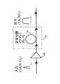
図5は図4に示される光クロック再生器28の実施形態を示すブロック図である。このクロック再生器は、入力ポート38及び出力ポート40間に設けられる光パス42と、光パス42に光学的に結合される(例えば方向性結合される)光ループ43を含む能動リングレーザ44とを備えている。
【0090】
入力ポート38には波長λS、速度fSの信号光(第2の光信号)が供給される。能動リングレーザ44は、光ループ43でレーザ発振が生じるように光ループ43の損失を補償する光増幅器46と、速度(又は周波数)fSが光ループ43の周回周期の逆数の整数倍になるように光ループ43の光路長を調節する調節器48と、信号光に基きレーザ発振をモードロックするための光変調器(又は非線形光学媒質)50とを含む。能動リングレーザ44はレーザ発振の波長λPを含む通過帯域を有する光帯域通過フィルタ43を更に含んでいても良い。
【0091】
この構成によると、能動リングレーザ44のレーザ発振がモードロックされる結果、波長λP、周波数fSのクロックパルスが発生し、そのクロックパルスが出力ポート40から出力される。従って、光/電気変換を行なうことなしにクロックパルスを得ることができ、信号光の速度やパルス形状等に依存しない全光クロック再生器の提供が可能になる。
【0092】
光変調器50としては、LiNbO3強度変調器やEA(電界吸収)型変調器等の電気/光変調器を用いることができるほか、二次若しくは三次の非線形光学効果或いは相互利得変調等によるものを用いることができる。例えば、光ファイバ内の四光波混合を用いる場合であれば、信号光の波長λSをファイバの零分散波長付近の波長に設定して連続発振光に効果的にAM変調をかけ、これによりクロックパルスを発生可能である。一方、半導体光アンプ(SOA)を用いる場合には、信号光をポンプ光として用いることができる。更に、発振状態のDFB−LD内の四光波混合を用いる場合には、信号光の波長をDFB−LDの発振光とは異なる波長に設定し、この信号光を比較的高いパワーで入力することにより利得飽和を起こし、これにより四光波混合の効率に変調をかけると共に、相互利得変調(XGM)効果により連続発振光に有効にAM変調をかけることができる。XGMについては、SOA内の四光波混合を用いる場合にも発生するので、これを積極的に用いても良い。
【0093】
また、2次の非線形光学効果の場合にも、信号光をポンプ光として用いれば、ほぼ同じ効果を得ることができる。一方、相互位相変調(XPM)を用いる場合には、例えば位相変調による偏波状態の変動を用いてAM変調を発生させることができる。
【0094】
波形整形器26は光パルスのジッタを抑圧するためのものである。その動作原理を理解する上で、こうした波形整形を行わない場合について考察する。信号光は時間的な乱れを含んでいるから、光ANDゲート4においてクロックパルスと同期する部分と多少ずれる部分が存在する。例えば、光ANDゲート4としてNOLM(非線形光ループミラー)のような高速光スイッチを用いる場合には、前述の時間的なずれにより、得られる変換光の振幅が一定でなくなる。従って、時間的なずれの原因がジッタのような雑音的なものであると、変換光には振幅雑音が付加されてしまう。
【0095】
そこで、本実施形態では、こうした雑音の付加を回避するために、光ANDゲート4に入力する信号光のパルス形状を矩形化している。これにより、この矩形パルスの幅の中では常にクロックパルスとの光AND動作が可能になるので、上述のような振幅雑音の付加を抑えることができ、その結果、ジッタ等の雑音を抑圧することができる。
【0096】
図6は図4に示される波形整形器26の実施形態を示すブロック図である。非線形光学効果を提供する光導波構造54として、光ファイバ56が用いられている。光ファイバ56のGVD(群速度分散)はβ2であり、光ファイバ56は例えば供給された信号光に正常分散及び3次の非線形光学効果を与える。
【0097】
中心波長λSを有する入力パルス(第1の光信号)は、光増幅器52により所要のチャーピングを発生させるのに十分な程度のパワーまで増幅された後、光ファイバ56に入力される。光ファイバ56内においては、SPM(自己位相変調)によりチャーピングが発生し、スペクトルが拡大(拡散)される。
【0098】
光ファイバ56内においては、SPM(自己位相変調)によりチャープし、光パルスの立上がり部では長波長側へのシフトが発生し、一方、光パルスの立下り部では短波長側へのシフトが発生する。例えば、用いる光ファイバが正常分散ファイバの場合には、波長が長いほど群速度が大きくなるため、上記チャープにより光パルスの幅は広がる。矩形状に広げるためには、短い長さで急激に波形が変化するように用いる光ファイバの分散値を適度に大きくし、そのような光ファイバに立上がり/立下がりの傾斜ができるだけ急峻な光パルスを高いパワーで入力すればよい。
【0099】
実際には、3次の非線形効果が有限であるため、ある程度の長さが必要であり、上記チャープに起因するパルス広がり以外にも、波長分散だけに起因するパルス広がりが特に比較的非線形効果の小さな光パルスの裾部分で発生する。このような場合には、波長分散に起因する広がり分を補償して所望の形状に近い光パルスを得るために、光ファイバの出力端に分散補償器を配置するとよい。例えば、逆符号の分散を有する光ファイバ等を配置することにより、効果的に分散を補償することができる。尚、光ファイバの分散値や補償量については、入力光パルスや用いる光ファイバ等の条件により、適宜調整することができる。
【0100】
尚、この正常分散ファイバを用いた矩形パルスの生成方法に関する付加的な詳細は、例えば特願2000−34454に記載されている。また、図6により説明した正常分散領域で光ファイバを用いて矩形パルスを得る方法以外には、例えば、ファイバーグレーティングを用いる方法、光パルスを直交2偏波に分けて時間的な遅延をさせた後に加え合わせる方法等もある。
【0101】
図7を参照すると、本発明が適用される光ファイバ伝送システムが示されている。送信機62からの信号光を第1の光ファイバ伝送路64により伝送し、この伝送された信号光を本発明による装置66で処理した後、得られた再生光を第2の光ファイバ伝送路68により受信機70に向けて更に伝送するものである。
【0102】
本発明による装置66での処理の結果、信号光に関する波形整形等が可能である。即ち、第1の光ファイバ伝送路64での伝送により品質が劣化した信号光を本発明による装置66で光3R再生することにより品質が改善され、伝送処理の拡張が可能になる。
【0103】
図示はしないが、光ファイバ伝送路64及び/又は68に沿って単一又は複数の光増幅器を配置して、損失を補償するようにシステムを構成してもよい。
【0104】
本発明は以下の付記を含むものである。
【0105】
(付記1) 第1の波長を有する信号光及び前記第1の波長と異なる第2の波長を有するプローブ光が入力され前記プローブ光を前記信号光で相互位相変調することでスペクトル拡大した光を出力する非線形光学媒質と、
前記非線形光学媒質により前記スペクトル拡大した光から前記信号光の変調成分が含まれ且つ前記スペクトル拡大された光の帯域幅よりも狭い帯域を有する光を抽出する光フィルタと
を備えた光ANDゲート。
【0106】
(付記2) 付記1記載の光ANDゲートの出力を自己位相変調によりスペクトル拡大した光を出力する第2の非線形光学媒質と、
前記第2の非線形光学媒質により前記スペクトル拡大した光から前記光ANDゲートの出力の信号成分が含まれ且つ前記スペクトル拡大された光の帯域幅よりも狭い帯域を有する光を抽出する第2の光フィルタと
を設けたことを特徴とする波形整形装置。
【0107】
(付記3) 付記1記載の光ANDゲートの出力光と前記光ANDゲートの出力光波長と異なる波長の第2プローブ光を入力し、前記第2プローブ光を前記光ANDゲートの出力光で相互位相変調することでスペクトル拡大した光を出力する第2の非線形光学媒質と、
前記第2の非線形光学媒質により前記スペクトル拡大した光から前記光ANDゲートの出力の信号成分が含まれ且つ前記スペクトル拡大された光の帯域幅よりも狭い帯域を有する光を抽出する第2の光フィルタと
を設けたことを特徴とする波形整形装置。
【0108】
(付記4) 光ANDゲートと、
該光ANDゲートの出力光と該光ANDゲートの出力光波長と異なる波長のプローブ光が入力され、前記プローブ光を前記光ANDゲートの出力光で相互位相変調することでスペクトル拡大した光を出力する非線形光学媒質と、
前記非線形光学媒質により前記スペクトル拡大された光から前記光ANDゲートの出力の信号成分が含まれ且つ前記スペクトル拡大された光の帯域幅よりも狭い帯域を有する光を抽出する光フィルタと
を設けたことを特徴とする波形整形装置。
【0109】
(付記5) 付記1、付記2、付記3、付記4記載の光ANDゲートは伝送路からの信号光のパルス幅を拡大した光と該伝送路からの信号光より抽出した光クロックを入力することを特徴とのする光ANDゲート及び波形整形装置。
【0110】
(付記6) 付記1、付記2、付記3、付記4記載の非線型光学媒質は単一モード光ファイバであることを特徴とする光ANDゲート及び波形整形装置。
【0111】
(付記7) 第1の波長を有する信号光及び前記第1の波長と異なる第2の波長を有するプローブ光が入力され前記プローブ光を前記信号光で相互位相変調するステップと、
前記スペクトル拡大した光から前記信号光の変調成分が含まれ且つ前記スペクトル拡大された光の帯域幅よりも狭い帯域を有する光を抽出するステップと
からなる波形整形方法。
【0112】
(付記8) 付記7記載の方法により得た出力を自己位相変調によりスペクトル拡大するステップと、
前記スペクトル拡大した光から信号成分が含まれ且つ前記スペクトル拡大された光の帯域幅よりも狭い帯域を有する光を抽出するステップ
からなる波形整形方法。
【0113】
(付記9) 付記8記載の方法により得た出力光とその出力光波長と異なる波長の第2プローブ光を入力し、前記第2プローブ光を前記付記1の方法により得た光で相互位相変調することでスペクトル拡大した光を出力するステップと、
前記スペクトル拡大した光から信号成分が含まれ且つ前記スペクトル拡大された光の帯域幅よりも狭い帯域を有する光を抽出するステップ
からなる波形整形方法。
【0114】
(付記10) 入力信号光を分岐し一方を波形整形し他方を光クロック抽出し、
波形整形した光と光クロック入力してAND条件で光クロックのスペクトル拡大し拡大した範囲の中で所定の帯域を切り出す手段と、
該手段の出力をスペクトル拡大し所定の帯域を切り出す手段とを有する波形整形装置。
【0115】
(付記11) 付記10の装置を送信機と受信機を接続する光伝送路の間に設けることを特徴とする光通信システム。
【0116】
【発明の効果】
以上説明したように、本発明によると、スペクトル拡大とフィルタリングにより振幅雑音を取り除くとともに、任意の波長へ波長変換を行うことができる。
【0117】
従って、十分な2R及び/又は3R機能、更には超高速な光スイッチングの機能を得ることができる波形整形のための方法及び装置を提供することが可能になるという効果が生じる。
【図面の簡単な説明】
【図1】 図1は本発明による装置の基本構成を示すブロック図である。
【図2】 図2は本発明による装置の実施形態を示すブロック図である。
【図3】 図3は本発明に適用可能な波長変換器の実施形態を示すブロック図である。
【図4】 図4は本発明による装置の他の実施形態を示すブロック図である。
【図5】 図5は本発明に適用可能なクロック再生器の実施形態を示すブロック図である。
【図6】 図6は本発明に適用可能な波形整形器の実施形態を示すブロック図である。
【図7】 図7は本発明が適用される光ファイバ伝送システムの実施形態を示すブロック図である。
【図8】 図8は本発明に適用可能な波長変換器の実施形態を示すブロック図である。
【符号の説明】
4 光ANDゲート
6 波長変換器
26 波形成形器
28 光クロック再生器
64,68 光ファイバ伝送路[0001]
BACKGROUND OF THE INVENTION
In the present invention, signal light has a waveformShaping In particular, the invention relates to an optical AND gate that performs optical signal regeneration using an optical signal and an optical clock.
[0002]
[Prior art]
In an optical fiber communication system that has been put into practical use in recent years, a decrease in signal power due to transmission line loss, branch loss, and the like is compensated by using an optical amplifier such as an erbium-doped fiber amplifier (EDFA). The optical amplifier is an analog amplifier and linearly amplifies a signal. In this type of optical amplifier, since the signal-to-noise ratio (S / N ratio) is reduced by the addition of spontaneous emission (ASE) noise generated along with amplification, the number of relays and thus the transmission distance is limited. Waveform degradation due to the chromatic dispersion of the optical fiber and the nonlinear optical effect in the fiber is also a factor that gives a transmission limit. In order to overcome these limitations, a regenerative repeater that digitally processes signals is required, and its realization is desired. In particular, an all-optical regenerative repeater that performs all processing at the optical level is important in realizing a transparent operation that does not depend on the bit rate or pulse shape of the signal.
[0003]
The functions required for an all-optical regenerative repeater include amplitude regeneration or reamplification, and waveformShaping Or, reshaping and timing recovery or retiming. These functions are called 3R functions, and in particular, the former two are called 2R functions.
[0004]
As a device that reproduces optical signals at the optical level, optical signals are converted into electrical signals, and after signal regeneration at the electrical stage, the laser light is modulated using the reproduced electrical signals and converted into optical signals.・ Electric / optical (O / E / O) conversion type and all-optical type that reproduces signal at optical level without conversion to electric signal. Of these, the O, E, and O types have already been put to practical use up to about 10 Gb / s, but the performance depends on the operation speed of the electronics, so that the operation at 40 Gb / s or more is difficult. On the other hand, the all-optical type is not practically used at present, but several methods have been proposed.
[0005]
A typical all-optical type is a Mach-Zehnder interferometer (MZI) type optical gate. This optical gate is configured by integrating MZI including first and second nonlinear optical media for providing a phase shift, for example, on an optical waveguide substrate. Continuous wave (CW) light or probe light as an optical pulse is equally distributed and supplied to the first and second nonlinear optical media. At this time, the optical path length of the interferometer is set so that output light is not obtained due to interference of the equally distributed probe light.
[0006]
Signal light is further supplied to one of the first and second nonlinear optical media. By appropriately setting the power of the signal light and the probe light, a converted optical signal synchronized with the signal light is output from the optical gate. The converted optical signal has the same wavelength as the probe light.
[0007]
It has been proposed to use a semiconductor optical amplifier (SOA) as each of the first and second nonlinear optical media. For example, in a 1.5 μm wavelength band, InGaAs-SOA whose both end faces are made non-reflective is used as each nonlinear optical medium, and these are integrated on an InP / GaInAsP substrate. In particular, in order to improve the operation speed, a type called an ultrafast nonlinear interferometer (UNI) has been proposed. This is because the timing of the optical pulse passing through the two optical paths of the interferometer is slightly shifted to improve the operating speed limit due to the carrier effect of the semiconductor medium.
[0008]
Other known waveformsShaping There exists a nonlinear optical loop mirror (NOLM) as an apparatus. The NOLM includes a first optical coupler including first and second optical paths that are directionally coupled, a loop optical path that connects the first and second optical paths, and a third optical path that is directionally coupled to the loop optical path. Including a second optical coupler.
[0009]
A part or the whole of the optical path of the loop is made of a nonlinear optical medium, and the converted optical signal is output from the second optical path by supplying probe light and signal light to the first and third optical paths, respectively.
[0010]
An optical fiber is generally used as a nonlinear optical medium in NOLM. In particular, NOLM using SOA as a nonlinear optical medium is called SLALOM (Semiconductor Laser Amplifier in a Loop Mirror).
[0011]
[Problems to be solved by the invention]
WaveformShaping A 3R function can be provided by combining the device and the optical clock recovery device. In this case, generally, the signal light to be reproduced 3R and the reproduction optical clock pulse are input to the optical AND gate, and the data of the signal light is transferred to the reproduction optical clock by the AND operation. WaveformShaping Is the waveform before or after input to the optical AND gateShaping Perform using equipment or waveform on optical AND gateShaping This is possible by combining functions.
[0012]
Waveform to provide optical 3R functionShaping In the apparatus, there is a problem that a sufficient 3R function may not be obtained depending on the relative positional deviation between the signal light input to the optical AND gate and the reproduction optical clock pulse on the time axis. Possible causes of such relative displacement include walk-off between the signal light and the regenerated optical clock pulse in the optical AND gate, temporal stability of each optical pulse, jitter, and the like.
[0013]
The 3R function proposed so far includes, for example, the one based on the above-described MZI type optical gate switch. We have previously provided waveforms to provide 2R and / or 3R functionsShaping An apparatus has been proposed (Japanese Patent Application No. 11-293189). In this device, the waveform is obtained by combining two NOLMs.Shaping Alternatively, the degree of freedom of wavelength conversion is increased when obtaining the function of the optical gate. However, in order to perform wavelength conversion using the above-described optical AND gate such as NOLM or an optical regenerative repeater, it is necessary to transmit the input probe light at a wavelength to be finally obtained. There is a problem that the wavelength that can be converted by the laser that transmits the light is determined.
[0014]
Therefore, an object of the present invention is to provide a method and an apparatus for easily converting the wavelength when performing the optical 3R function into an arbitrary wavelength. Other objects of the present invention will become clear from the following description.
[0015]
[Means for Solving the Problems]
An optical AND gate according to a first aspect of the present invention receives signal light having a first wavelength and probe light having a second wavelength different from the first wavelength, and cross-phase modulates the probe light with the signal light. A non-linear optical medium that outputs light whose spectrum has been expanded in the above, and light that includes a modulation component of the signal light from the light whose spectrum has been expanded by the non-linear optical medium and that has a narrower bandwidth than the bandwidth of the spectrum-expanded light And the optical power of the signal light input to the nonlinear optical medium is 10 to 100 times the power of the probe light, and the nonlinear optical medium comprises an optical fiber, The wavelength of the probe light is located in the anomalous dispersion region of the optical fiber.The wavelength of the signal light is an anomalous dispersion region of the optical fiber, and the walk-off between the signal light and the probe light is kept small. .
[0016]
In the configuration of the first invention, the probe light expands the spectrum in the nonlinear optical medium in the optical AND gate, and the signal component is newly extracted from the light whose spectrum has been expanded. An arbitrary wavelength can be output from the optical AND gate without change. Therefore, the degree of freedom of wavelength conversion can be increased.
[0017]
Furthermore, since the fluctuation of the output level is suppressed by the spectrum expansion, the amplitude noise of the signal light can be suppressed.
[0018]
Therefore, optical signal processing such as optical 3R processing, wavelength conversion processing, and optical demultiplexing processing can be stably performed even for ultrahigh-speed signals.
[0019]
Waveform of the second inventionShaping The deviceAn optical AND gate of the first invention; A second nonlinear optical medium that outputs light whose spectrum is expanded by self-phase modulation of the output of the optical AND gate, and a signal component of the output of the optical AND gate from the light whose spectrum is expanded by the second nonlinear optical medium And a second optical filter for extracting light having a band narrower than the bandwidth of the spectrum-expanded light.
[0020]
According to the configuration of the second invention, the wavelength converted into an arbitrary wavelength by the optical AND gate of the first invention is further subjected to self-phase modulation by the second nonlinear optical medium, and the spectrum of the output light is expanded, Since a new signal component is extracted therefrom, the degree of freedom in wavelength conversion can be further increased. With this configuration, it is possible to convert to the same wavelength as the signal light input to the optical AND gate, and it is possible to obtain signal light with reduced amplitude noise at the signal light wavelength input to the optical AND gate. Furthermore, since the fluctuation of the output level is suppressed by enlarging the spectrum of the output light by self-phase modulation, the amplitude noise of the signal light can be suppressed as compared with the optical AND gate alone.
[0021]
Waveform of the third inventionShaping The deviceAn optical AND gate of the first invention; The spectrum is expanded by inputting the output light of the optical AND gate and the second probe light having a wavelength different from the output light wavelength of the optical AND gate, and cross-phase-modulating the second probe light with the output light of the optical AND gate. A second nonlinear optical medium that outputs light, and a signal component of an output of the optical AND gate from the light whose spectrum is expanded by the second nonlinear optical medium, and more than a bandwidth of the spectrum-expanded light And a second optical filter for extracting light having a narrow band.
[0022]
According to the configuration of the third invention, since the output light of the optical AND gate is cross-phase modulated by the probe light, an arbitrary wavelength can be output in the optical AND gate without changing the wavelength of the probe light. The degree of freedom of wavelength conversion can be increased. With this configuration, it is possible to convert to the same wavelength as the signal light input to the optical AND gate, and it is possible to obtain signal light with reduced amplitude noise at the signal light wavelength input to the optical AND gate. Further, since the output level fluctuation is suppressed by the spectrum expansion of the output light of the optical AND gate and the probe light by cross phase modulation, the amplitude noise of the signal light can be suppressed more than the optical AND gate alone.
[0025]
First4, 5 Optical AND Gate and Waveform of InventionShaping The device is an optical AND gate of the first invention, the second invention, and the third invention.Oh In this configuration, light having an expanded pulse width of signal light from the transmission path and an optical clock extracted from the optical signal from the transmission path are input. First4, According to the invention of 5, the optical AND gate and the waveformShaping Amplitude noise generated in the optical AND gate due to jitter and temporal instability of the signal light and clock pulse of the device can be suppressed.
[0026]
DETAILED DESCRIPTION OF THE INVENTION
Hereinafter, exemplary embodiments of the present invention will be described in detail with reference to the accompanying drawings. Throughout the drawings, substantially the same or similar parts are denoted by the same reference numerals.
[0027]
In a preferred embodiment of the present invention, in the optical AND gate, the probe light is subjected to cross-phase modulation (XPM) with the signal light, thereby expanding the spectrum of the probe light, and a component different from the spectrum center wavelength from the spectrum. By extracting with a band pass filter, a signal component subjected to wavelength conversion is extracted.
[0028]
Then, for example, the wavelength-converted signal component is further wavelength-converted to match the wavelength of the original signal light or to be converted to an arbitrary wavelength. In this wavelength conversion, a method of expanding a spectrum by self-phase modulation (SPM) and extracting a component different from the center wavelength of the spectrum by an optical bandpass filter can be used. By this method, the waveform for amplitude noise suppressionShaping Can be applied to the signal light.
[0029]
As a wavelength conversion method, a method of expanding the spectrum by cross phase modulation (XPM) can also be used.
[0030]
As the probe light of the optical AND gate or wavelength converter for performing XPM, continuous wave light (CW light) or an optical pulse train can be used, and in particular, an optical clock pulse regenerated from the original signal light is also used as the optical pulse train. You can also.
[0031]
According to the present invention, it is possible to suppress amplitude noise, jitter, and the like of signal light, and it is possible to provide an optical signal processing device such as an optical 3R device, a wavelength conversion device, and an optical demultiplexer even for an ultrahigh-speed signal. .
[0032]
Referring to FIG. 1, the basic configuration of the above-described preferred embodiment of the present invention is shown.
[0033]
Wavelength λS Are amplified to an appropriate power by an
[0034]
Wavelength λ obtained by logical product due to nonlinear optical effect in optical AND gate 4S 'Converted light is output from the optical AND
[0035]
The
[0036]
The optical AND
[0037]
FIG. 2 is a block diagram showing an embodiment of an apparatus using an optical AND
[0038]
The optical AND
[0039]
When a light pulse is input to the nonlinear optical medium, chirping by XPM occurs, and the spectrum of the probe light is expanded.
[0040]
As shown at the top of FIG. 2, the wavelength λS Input signal light and wavelength λP Are combined by the
[0041]
As the probe light, continuous wave light (CW light) or an optical pulse train as shown in FIG. 2 can be used. In particular, an optical clock pulse regenerated from the original signal light can also be used as the optical pulse train.
[0042]
In the
[0043]
And within this expanded spectrum, the wavelength λP Different from λS A signal component is extracted by the optical bandpass filter 12 having a passband with ′ as the center wavelength. The passband is set narrower than the expanded spectrum.
[0044]
At this time, even if the amplitude of the signal light, which should normally be constant, varies from pulse to pulse due to distortion due to transmission or the like (amplitude fluctuation or amplitude noise), the spectrum is constant in the range where chirping occurs, It is possible to suppress amplitude fluctuation. That is, the waveformShaping This function is obtained.
[0045]
More specifically, the optical bandpass filter 12 removes components with small chirping and components larger than necessary for chirping. The small chirping component mainly includes a fluctuation component from the zero point of the off-power (zero sign) component (for example, waveform degradation due to GVD) and a small slope component near the peak of the pulse.
[0046]
On the other hand, components with larger chirping than necessary mainly include fluctuation components with a large slope near the peak of the on-power (1 code) component. Since these components determine the optical signal-to-noise ratio (OSNR), by removing this portion by the optical bandpass filter 12, the OSNR due to power fluctuations, extinction ratio degradation, noise accumulation, etc. of these components. Can be reduced. Therefore, according to the present invention, it is possible to perform wavelength conversion with an improvement in OSNR.
[0047]
Center wavelength λ of the passband of the optical bandpass filter 12S ′ Is the center wavelength λ of the probe light so that the output signal pulse does not include a component with a small chirp including noise and a component with a chirp larger than necessaryP It is desirable to keep it sufficiently away from
[0048]
When signal light having amplitude fluctuation is input, amplitude noise is larger at the position of the wavelength λp of the probe light than at other wavelengths. Therefore, it is necessary to remove that part. Further, since there is a lot of noise at the shortest wavelength side and long wavelength side edge portions of the spectrum-expanded light, it is desirable to avoid it.
[0049]
The width and shape of the passband of the optical bandpass filter 12 are preferably set as appropriate according to the required pulse width and shape. Basically, it is desirable that the input signal is set to be approximately equal to the spectrum width before being input to the transmission line and deteriorated.
[0050]
An optical fiber (including a normal single mode optical fiber) can be used as a material for the nonlinear optical medium.
[0051]
In particular, highly nonlinear fibers and photonic crystal fibers (Holey Fiber) are suitable.
[0052]
These optical fibers have a third-order nonlinear coefficient γ of 2 (W-1 Km-1 ) (The phase rotates by 2 radians when 1 W optical power is input to a 1 km fiber), whereas the highly nonlinear fiber has a third-order nonlinear coefficient γ of about 20 (W-1 Km-1 ), The cubic nonlinear coefficient γ is about 100 (W-1 Km-1 ) Grades have been developed.
[0053]
The phase shift amount Δφ due to XPM is
Δφ = γPL (γ is the third-order nonlinear coefficient, P is the optical power, L is the length of the nonlinear medium)
It is.
[0054]
Therefore, even if the input power is increased, XPM and SPM are strongly generated. Therefore, it is an effective means to sufficiently increase the light input to the optical AND gate by the
[0055]
At this time, by setting the power Pλs of the input signal light wavelength λs to 10 to 100 times the power Pλp of the probe light wavelength λp, the probe light wavelength λp side can be efficiently cross-phase modulated. it can.
[0056]
The cubic nonlinear coefficient γ is
γ = 2πn2 / λAeff (n2 Is expressed as a nonlinear refractive index, Aeff is an effective cross-sectional area, and λ is a wavelength) .By reducing the effective cross-sectional area, which is the area of light propagation in the nonlinear optical medium, the input power is substantially reduced. The same effect as when strengthening can be obtained. Although the optical filter is described as a fixed band-pass filter in FIG. 2, the signal light may be cut out using a variable optical filter.
[0057]
If the amplitude noise is reduced and the wavelength is simply converted to an arbitrary wavelength, the configuration shown in FIG. 2 is sufficient. However, the wavelength of the input signal light is returned to the original wavelength or outside the spectrum range expanded by XPM. If it is desired to set wavelength conversion, the output of the optical AND
[0058]
A specific configuration of the
[0059]
In FIG. 3, the wavelength λS The converted light of ′ is amplified to an appropriate power by the
[0060]
By this wavelength conversion, the remaining amplitude fluctuation can be further suppressed even by the optical AND gate 4 (see FIG. 1). The principle that the amplitude fluctuation is suppressed is the same as that in the above-mentioned XPM, and the description thereof is omitted.
[0061]
FIG. 8 shows another configuration of the
[0062]
The
[0063]
The converted light λs ′ from the
[0064]
The CW light λp ′ is expanded in spectrum by XPM by the converted light λs ′ in the
[0065]
By cutting out the wavelength λs of the signal light having a spectrum spread around the wavelength λp ′ by the XPM by the optical filter 201, the wavelength of the reproduction light can be set to λs.
[0066]
At this time, the wavelength of the selected wavelength of the optical filter 201 is set to an arbitrary position of the signal light having a spread spectrum centered on the wavelength λp ′, thereby returning the wavelength to the signal light wavelength λs input to the optical signal reproducing device. Can also be converted to other wavelengths.
[0067]
By such wavelength conversion, it is possible to further suppress the amplitude fluctuation remaining even by the conversion by the optical AND
[0068]
In order to effectively generate XPM in the
[0069]
Also, since the optical S / N ratio of the reproduction light λs is proportional to the power level of the CW light λp ′, the CW light λp ′ input to the
[0070]
The relationship between the output powers of the optical amplifiers is the same as the relationship shown in FIG. 2, and increasing the power of the converted light λs ′ is effective in performing XPM.
[0071]
When the configurations of FIGS. 3 and 8 are used as the
[0072]
Further, the configuration shown in FIGS. 3 and 8 can be used in combination for signal output such as optical-electrical-optical conversion.
[0073]
As described above, for example, in the embodiment shown in FIG. 1, the optical AND
[0074]
Furthermore, the dispersion of the optical fiber used as the nonlinear optical medium described in FIGS. 2, 3, and 8 is important.
[0075]
First, from the viewpoint of effectively expanding the spectrum, it is better to set the dispersion of the wavelength λp to be small and an anomalous dispersion region. However, when the dispersion is too small and close to zero, ASE (spontaneously emitted light) noise generated from an optical amplifier or the like is nonlinearly amplified (modulation unstable), and the S / N deteriorates. In order to ensure a high S / N, it is effective to use an optical fiber in the normal dispersion region, but in this case, the spectrum expansion is limited.
[0076]
Therefore, an optimum dispersion is selected for each system, such as selecting an anomalous dispersion region when priority is given to a large wavelength shift and selecting a normal dispersion region when priority is given to a high S / N even if the wavelength shift is small. It is good to set.
[0077]
On the other hand, when an optical pulse train is used as the probe light, it is desirable to reduce the walk-off between the signal light and the probe light in the optical fiber 10 (see FIG. 2) that generates XPM.
[0078]
From this point of view, the smaller the dispersion, the better. For example, a method in which both the wavelength of the signal light and the wavelength of the probe light are arranged in the normal dispersion region or the anomalous dispersion region, a method of arranging both wavelengths symmetrically with zero dispersion in order to minimize the walk-off, and further dispersion. There are a method using a flat fiber and a method using dispersion compensation.
[0079]
FIG. 4 is a block diagram showing another embodiment of the apparatus according to the present invention. This device includes an
[0080]
As the optical AND
[0081]
WaveformShaping The optical signal (input signal light) having the wavelength λs to be processed is amplified by the
[0082]
The first signal light has a waveformShaping Waveform obtained by enlarging the pulse width of the first signal light supplied to the
[0083]
The second signal light is supplied to the
[0084]
WaveformShaping The optical and clock pulses are supplied to the optical AND
[0085]
The wavelength of the converted signal light is changed by the
[0086]
The
[0087]
For example, in the case of 160 Gb / s signal light, a 160 GHz pulse train arranged at intervals of 6.25 ps is reproduced. Use a method of electrically timing recovery after O / E conversion and oscillating a mode-locked laser (MLL) using the electrical RF signal, or a method of directly oscillating MLL without conversion to electricity. Can do.
[0088]
However, in the case of a high-speed signal such as 160 Gb / s, the operating speed limit of the electronics is exceeded, and it is difficult to realize an MLL that operates at such a speed. Therefore, it is desirable to generate a 160 GHz clock pulse by regenerating a lower-speed pulse train of 10 GHz, for example, by OTDM (optical time division multiplexing).
[0089]
FIG. 5 is a block diagram showing an embodiment of the
[0090]
The
[0091]
According to this configuration, as a result of the mode-locking of the laser oscillation of the
[0092]
As the
[0093]
Also in the case of the second-order nonlinear optical effect, substantially the same effect can be obtained if signal light is used as pump light. On the other hand, when cross phase modulation (XPM) is used, AM modulation can be generated using, for example, a change in polarization state due to phase modulation.
[0094]
WaveformShaping The
[0095]
Therefore, in this embodiment, in order to avoid the addition of such noise, the pulse shape of the signal light input to the optical AND
[0096]
6 shows the waveform shown in FIG.Shaping FIG. 6 is a block diagram showing an embodiment of the
[0097]
Center wavelength λS Is amplified to a power sufficient to generate the required chirping by the optical amplifier 52, and then input to the
[0098]
In the
[0099]
Actually, since the third-order nonlinear effect is finite, a certain length is required, and in addition to the pulse broadening caused by the chirp, the pulse broadening caused by only the chromatic dispersion has a relatively nonlinear effect. It occurs at the bottom of a small light pulse. In such a case, a dispersion compensator may be disposed at the output end of the optical fiber in order to obtain a light pulse close to a desired shape by compensating for the spread due to chromatic dispersion. For example, the dispersion can be effectively compensated by arranging an optical fiber or the like having dispersion of the opposite sign. The dispersion value and compensation amount of the optical fiber can be appropriately adjusted according to the conditions of the input light pulse, the optical fiber to be used, and the like.
[0100]
Additional details regarding the rectangular pulse generation method using the normal dispersion fiber are described in, for example, Japanese Patent Application No. 2000-34454. In addition to the method of obtaining a rectangular pulse using an optical fiber in the normal dispersion region described with reference to FIG. 6, for example, a method using a fiber grating, the optical pulse is divided into two orthogonal polarizations, and a time delay is made. There is also a method of adding them later.
[0101]
Referring to FIG. 7, an optical fiber transmission system to which the present invention is applied is shown. The signal light from the
[0102]
As a result of processing in the
[0103]
Although not shown, the system may be configured to compensate for losses by placing single or multiple optical amplifiers along the optical
[0104]
The present invention includes the following supplementary notes.
[0105]
(Supplementary note 1) Signal light having a first wavelength and probe light having a second wavelength different from the first wavelength are input, and light whose spectrum is expanded by cross-phase-modulating the probe light with the signal light is added. An output nonlinear optical medium;
An optical filter for extracting light including a modulation component of the signal light from the light whose spectrum is expanded by the nonlinear optical medium and having a band narrower than the bandwidth of the light whose spectrum is expanded;
Optical AND gate with
[0106]
(Additional remark 2) The 2nd nonlinear optical medium which outputs the light which expanded the spectrum of the output of the optical AND gate of Additional remark 1 by self phase modulation,
Second light for extracting light that includes a signal component of the output of the optical AND gate from the light whose spectrum has been expanded by the second nonlinear optical medium and has a band narrower than the bandwidth of the light whose spectrum has been expanded. Filter and
Waveform characterized by providingShaping apparatus.
[0107]
(Supplementary Note 3) The output light of the optical AND gate described in Supplementary Note 1 and the second probe light having a wavelength different from the output light wavelength of the optical AND gate are input, and the second probe light is mutually exchanged by the output light of the optical AND gate. A second nonlinear optical medium that outputs light whose spectrum is expanded by phase modulation;
Second light for extracting light that includes a signal component of the output of the optical AND gate from the light whose spectrum has been expanded by the second nonlinear optical medium and has a band narrower than the bandwidth of the light whose spectrum has been expanded. Filter and
Waveform characterized by providingShaping apparatus.
[0108]
(Appendix 4) Optical AND gate,
The output light of the optical AND gate and the probe light having a wavelength different from the output light wavelength of the optical AND gate are input, and the spectrum expanded light is output by cross-phase modulating the probe light with the output light of the optical AND gate. A non-linear optical medium,
An optical filter that extracts light including a signal component of an output of the optical AND gate from the light whose spectrum is expanded by the nonlinear optical medium and having a band narrower than the bandwidth of the spectrum-expanded light;
Waveform characterized by providingShaping apparatus.
[0109]
(Additional remark 5) The optical AND gate of Additional remark 1,
[0110]
(Supplementary note 6) The optical AND gate and waveform, wherein the nonlinear optical medium described in supplementary note 1,
[0111]
(Supplementary note 7) A step of inputting a signal light having a first wavelength and a probe light having a second wavelength different from the first wavelength, and cross-phase-modulating the probe light with the signal light;
Extracting light including a modulation component of the signal light from the spectrum-expanded light and having a band narrower than a bandwidth of the spectrum-expanded light;
Waveform consisting ofShaping Method.
[0112]
(Supplementary note 8) The step of expanding the spectrum by self-phase modulation of the output obtained by the method of
Extracting light including a signal component from the spectrum-expanded light and having a band narrower than the bandwidth of the spectrum-expanded light.
Waveform consisting ofShaping Method.
[0113]
(Additional remark 9) The output light obtained by the method of
Extracting light including a signal component from the spectrum-expanded light and having a band narrower than the bandwidth of the spectrum-expanded light.
Waveform consisting ofShaping Method.
[0114]
(Supplementary note 10) The input signal light is split and one waveform isShaping And extract the other optical clock,
WaveformShaping Means for cutting out a predetermined band within a range in which the spectrum of the optical clock is expanded and expanded under AND conditions by inputting the light and the optical clock;
A waveform having means for expanding the spectrum of the output of the means and cutting out a predetermined bandShaping apparatus.
[0115]
(Additional remark 11) The optical communication system characterized by providing the apparatus of
[0116]
【The invention's effect】
As described above, according to the present invention, amplitude noise can be removed by spectrum expansion and filtering, and wavelength conversion to an arbitrary wavelength can be performed.
[0117]
Therefore, a waveform that can provide a sufficient 2R and / or 3R function, as well as an ultrafast optical switching function.Shaping The effect is that it becomes possible to provide a method and an apparatus for the above.
[Brief description of the drawings]
FIG. 1 is a block diagram showing the basic configuration of an apparatus according to the present invention.
FIG. 2 is a block diagram illustrating an embodiment of an apparatus according to the present invention.
FIG. 3 is a block diagram showing an embodiment of a wavelength converter applicable to the present invention.
FIG. 4 is a block diagram showing another embodiment of the device according to the invention.
FIG. 5 is a block diagram showing an embodiment of a clock regenerator applicable to the present invention.
FIG. 6 is a block diagram showing an embodiment of a waveform shaper applicable to the present invention.
FIG. 7 is a block diagram showing an embodiment of an optical fiber transmission system to which the present invention is applied.
FIG. 8 is a block diagram showing an embodiment of a wavelength converter applicable to the present invention.
[Explanation of symbols]
4 optical AND gate
6 Wavelength converter
26 Waveformer
28 Optical clock regenerator
64, 68 optical fiber transmission line
Claims (5)
Translated fromJapanese前記非線形光学媒質により前記スペクトル拡大した光から前記信号光の変調成分が含まれ且つ前記スペクトル拡大された光の帯域幅よりも狭い帯域を有する光を抽出する光フィルタとを備え、
前記非線形光学媒質に入力される前記信号光のパワーは前記プローブ光のパワーの10倍から100倍のパワーであり、
前記非線形光学媒質は光ファイバから成り、前記プローブ光の波長は前記光ファイバの異常分散領域に位置し、
前記プローブ光はパルス列であり、
前記信号光の波長は、前記光ファイバの異常分散領域であり、前記信号光と前記プローブ光のウオークオフを小さく抑える光ANDゲート。Nonlinear optics that outputs a signal light having a first wavelength and a probe light having a second wavelength different from the first wavelength and outputs a spectrum-expanded light by cross-phase-modulating the probe light with the signal light. Medium,
An optical filter that extracts light having a band narrower than the bandwidth of the spectrum-enhanced light and including a modulation component of the signal light from the spectrum-enhanced light by the nonlinear optical medium;
The power of the signal light input to the nonlinear optical medium is 10 to 100 times the power of the probe light,
The nonlinear optical medium is composed of an optical fiber, and the wavelength of the probe light is locatedin an anomalous dispersion region of the optical fiber,
The probe light is a pulse train,
The wavelength of the signal light is an anomalous dispersion region of the optical fiber, and an optical AND gatethat suppresses walk-off between the signal light and the probe light .
前記光ANDゲートの出力を自己位相変調によりスペクトル拡大した光を出力する第2の非線形光学媒質と、
前記第2の非線形光学媒質により前記スペクトル拡大した光から前記光ANDゲートの出力の信号成分が含まれ且つ前記スペクトル拡大された光の帯域幅よりも狭い帯域を有する光を抽出する第2の光フィルタと
を設けたことを特徴とする波形整形装置。An optical AND gate according to claim 1;
A second nonlinear optical medium that outputs light whose spectrum is expanded by self-phase modulation of the output of the optical AND gate;
Second light for extracting light that includes a signal component of the output of the optical AND gate from the light whose spectrum has been expanded by the second nonlinear optical medium and has a band narrower than the bandwidth of the light whose spectrum has been expanded. A waveform shaping device characterized by comprising a filter.
前記光ANDゲートの出力光と前記光ANDゲートの出力光波長と異なる波長の第2プローブ光を入力し、前記第2プローブ光を前記光ANDゲートの出力光で相互位相変調することでスペクトル拡大した光を出力する第2の非線形光学媒質と、
前記第2の非線形光学媒質により前記スペクトル拡大した光から前記光ANDゲートの出力の信号成分が含まれ且つ前記スペクトル拡大された光の帯域幅よりも狭い帯域を有する光を抽出する第2の光フィルタと
を設けたことを特徴とする波形整形装置。An optical AND gate according to claim 1;
The spectrum is expanded by inputting the output light of the optical AND gate and the second probe light having a wavelength different from the output light wavelength of the optical AND gate, and cross-phase-modulating the second probe light with the output light of the optical AND gate. A second nonlinear optical medium that outputs the transmitted light;
Second light for extracting light that includes a signal component of the output of the optical AND gate from the light whose spectrum has been expanded by the second nonlinear optical medium and has a band narrower than the bandwidth of the light whose spectrum has been expanded. A waveform shaping device characterized by comprising a filter.
Priority Applications (4)
| Application Number | Priority Date | Filing Date | Title |
|---|---|---|---|
| JP2002197109AJP4397567B2 (en) | 2002-07-05 | 2002-07-05 | Optical AND gate and waveform shaping device |
| US10/602,629US6987607B2 (en) | 2002-07-05 | 2003-06-25 | Optical AND gate and waveform shaping device |
| DE60309978TDE60309978T2 (en) | 2002-07-05 | 2003-07-03 | Optical device for waveform shaping |
| EP03014508AEP1379018B1 (en) | 2002-07-05 | 2003-07-03 | Optical waveform shaping device |
Applications Claiming Priority (1)
| Application Number | Priority Date | Filing Date | Title |
|---|---|---|---|
| JP2002197109AJP4397567B2 (en) | 2002-07-05 | 2002-07-05 | Optical AND gate and waveform shaping device |
Publications (2)
| Publication Number | Publication Date |
|---|---|
| JP2004037985A JP2004037985A (en) | 2004-02-05 |
| JP4397567B2true JP4397567B2 (en) | 2010-01-13 |
Family
ID=29720312
Family Applications (1)
| Application Number | Title | Priority Date | Filing Date |
|---|---|---|---|
| JP2002197109AExpired - Fee RelatedJP4397567B2 (en) | 2002-07-05 | 2002-07-05 | Optical AND gate and waveform shaping device |
Country Status (4)
| Country | Link |
|---|---|
| US (1) | US6987607B2 (en) |
| EP (1) | EP1379018B1 (en) |
| JP (1) | JP4397567B2 (en) |
| DE (1) | DE60309978T2 (en) |
Families Citing this family (39)
| Publication number | Priority date | Publication date | Assignee | Title |
|---|---|---|---|---|
| JP2005208515A (en)* | 2004-01-26 | 2005-08-04 | Sumitomo Electric Ind Ltd | Wavelength conversion method and wavelength converter |
| GB0402344D0 (en)* | 2004-02-03 | 2004-03-10 | Univ Aston | Optical pulse regenerator |
| US7245805B2 (en)* | 2004-03-23 | 2007-07-17 | The Research Foundation Of The City University Of New York | Method and apparatus for producing a multiple optical channel source from a supercontinuum generator for WDM communication |
| JP2006038960A (en)* | 2004-07-22 | 2006-02-09 | Fujitsu Ltd | Optical waveform monitoring device and oscilloscope |
| CN100353254C (en)* | 2004-09-01 | 2007-12-05 | 富士通株式会社 | Optical switch and optical waveform monitoring device utilizing optical switch |
| GB0427374D0 (en)* | 2004-12-15 | 2005-01-19 | Univ Aston | Optical pulse regeneration based on pulse temporal shaping |
| US7123407B2 (en)* | 2005-01-20 | 2006-10-17 | Korea Institute Of Science And Technology | Apparatus and method for realizing all-optical NOR logic device using gain saturation characteristics of a semiconductor optical amplifier |
| US7365855B2 (en)* | 2005-07-08 | 2008-04-29 | The Chinese University Of Hong Kong | Optical sensing devices with SPR sensors based on differential phase interrogation and measuring method using the same |
| GB2434483A (en)* | 2006-01-20 | 2007-07-25 | Fianium Ltd | High-Power Short Optical Pulse Source |
| US7409131B2 (en)* | 2006-02-14 | 2008-08-05 | Coveytech, Llc | All-optical logic gates using nonlinear elements—claim set V |
| US20070189703A1 (en)* | 2006-02-14 | 2007-08-16 | Coveytech, Llc | All-optical logic gates using nonlinear elements-claim set I |
| US7428359B2 (en)* | 2006-02-14 | 2008-09-23 | Coveytech, Llc | All-optical logic gates using nonlinear elements—claim set IV |
| US7263262B1 (en)* | 2006-02-14 | 2007-08-28 | Coveytech, Llc | All-optical logic gates using nonlinear elements-claim set VI |
| US7664355B2 (en)* | 2006-02-14 | 2010-02-16 | Coveytech Llc | All-optical gates using nonlinear elements-claim set III |
| US7394958B2 (en)* | 2006-02-14 | 2008-07-01 | Coveytech, Llc | All-optical logic gates using nonlinear elements-claim set II |
| GB2446001A (en)* | 2006-12-22 | 2008-07-30 | Ericsson Telefon Ab L M | Label processing method for packetised optical signals using a plurality of probe signals and an optical AND gate |
| WO2008103841A1 (en)* | 2007-02-21 | 2008-08-28 | Seamobile, Inc. | Preventing mobile communications in a quiet zone using artificially imposed signal time delay |
| JP5056095B2 (en)* | 2007-03-20 | 2012-10-24 | 富士通株式会社 | Optical waveform control device, optical signal processing device, and optical repeater |
| WO2009047856A1 (en)* | 2007-10-11 | 2009-04-16 | Fujitsu Limited | Optical pulse generator and optical signal processor |
| JP2010079246A (en)* | 2008-09-01 | 2010-04-08 | Furukawa Electric Co Ltd:The | Optical waveform regenerator and optical waveform regenerating method |
| WO2010148282A2 (en)* | 2009-06-18 | 2010-12-23 | Paul Prucnal | An optical switch using a michelson interferometer |
| US20100325513A1 (en)* | 2009-06-18 | 2010-12-23 | Peter Donegan | Integrated control electronics (ice) for a holographic storage system |
| WO2010148280A2 (en)* | 2009-06-18 | 2010-12-23 | Cadet, Gardy | Method and system for re-writing with a holographic storage medium |
| WO2010148281A2 (en)* | 2009-06-18 | 2010-12-23 | Cadet, Gardy | Method and apparatus for bulk erasure in a holographic storage system |
| US8315489B2 (en)* | 2009-06-18 | 2012-11-20 | Paul Prucnal | Optical sensor array |
| US8456730B2 (en)* | 2009-06-18 | 2013-06-04 | Access Optical Networks, Inc. | Directly modulated spatial light modulator |
| US20100322058A1 (en)* | 2009-06-18 | 2010-12-23 | Marvin Hutt | Holographic storage system using angle-multiplexing |
| DE102009050051A1 (en)* | 2009-10-21 | 2011-04-28 | Deutsche Telekom Ag | Method for delaying optical pulses |
| CN103091936B (en)* | 2013-01-23 | 2015-06-24 | 西安理工大学 | Method for achieving all-optical logic and operation based on light absorption bleaching effect |
| GB201407169D0 (en)* | 2014-04-23 | 2014-06-04 | Univ Aston | Nonlinear communication channel |
| US10187146B2 (en) | 2016-09-19 | 2019-01-22 | DISH Technologies L.L.C. | Light converting device |
| US9746632B1 (en) | 2016-09-19 | 2017-08-29 | Echostar Technologies L.L.C. | Light waveguide apparatus |
| JP7106835B2 (en) | 2017-10-06 | 2022-07-27 | 富士通株式会社 | Optical transmission device, wavelength conversion device, optical transmission method, and wavelength conversion method |
| US11444690B2 (en) | 2019-07-17 | 2022-09-13 | Lawrence Livermore National Security, Llc | Timing measurement apparatus |
| US11209714B2 (en) | 2019-07-17 | 2021-12-28 | Lawrence Livermore National Security, Llc | Radio frequency passband signal generation using photonics |
| US11159241B2 (en) | 2019-07-18 | 2021-10-26 | Lawrence Livermore National Security, Llc | High power handling digitizer using photonics |
| US11184087B2 (en) | 2019-08-08 | 2021-11-23 | Lawrence Livermore National Security, Llc | Optical encoder devices and systems |
| US11438086B2 (en)* | 2020-01-21 | 2022-09-06 | Fujitsu Limited | Optical amplification in an optical network |
| CN111780856B (en)* | 2020-06-01 | 2022-03-29 | 哈尔滨工业大学 | Optical fiber distributed vibration measurement method based on Rayleigh scattering spectrum phase spectrum analysis |
Family Cites Families (6)
| Publication number | Priority date | Publication date | Assignee | Title |
|---|---|---|---|---|
| US5150248A (en)* | 1989-07-21 | 1992-09-22 | Alfano Robert R | Terahertz repetition rate optical computing systems, and communication systems and logic elements using cross-phase modulation based optical processors |
| JP2000323786A (en)* | 1999-05-14 | 2000-11-24 | Fujitsu Ltd | Method, apparatus and system for waveform shaping of signal light |
| JP3882979B2 (en) | 1999-10-15 | 2007-02-21 | 富士通株式会社 | Apparatus and system for waveform shaping |
| JP4454763B2 (en)* | 2000-03-03 | 2010-04-21 | 富士通株式会社 | Method, apparatus and system for waveform shaping signal light |
| KR100425374B1 (en)* | 2001-11-14 | 2004-03-30 | 한국과학기술연구원 | Realization Method and Apparatus of All-Optical Half Adder by Using SOA-Based Devices |
| JP4094854B2 (en)* | 2002-01-09 | 2008-06-04 | 富士通株式会社 | Method and apparatus for waveform shaping of signal light |
- 2002
- 2002-07-05JPJP2002197109Apatent/JP4397567B2/ennot_activeExpired - Fee Related
- 2003
- 2003-06-25USUS10/602,629patent/US6987607B2/ennot_activeExpired - Fee Related
- 2003-07-03EPEP03014508Apatent/EP1379018B1/ennot_activeExpired - Lifetime
- 2003-07-03DEDE60309978Tpatent/DE60309978T2/ennot_activeExpired - Lifetime
Also Published As
| Publication number | Publication date |
|---|---|
| EP1379018A1 (en) | 2004-01-07 |
| US20040004780A1 (en) | 2004-01-08 |
| DE60309978T2 (en) | 2007-09-20 |
| EP1379018B1 (en) | 2006-11-29 |
| US6987607B2 (en) | 2006-01-17 |
| JP2004037985A (en) | 2004-02-05 |
| DE60309978D1 (en) | 2007-01-11 |
Similar Documents
| Publication | Publication Date | Title |
|---|---|---|
| JP4397567B2 (en) | Optical AND gate and waveform shaping device | |
| JP4094854B2 (en) | Method and apparatus for waveform shaping of signal light | |
| JP4401626B2 (en) | Method and apparatus for processing optical signals | |
| JP4472222B2 (en) | Method, apparatus and system for waveform shaping signal light | |
| JP3948598B2 (en) | Method, apparatus and system for processing optical signals | |
| JP4454763B2 (en) | Method, apparatus and system for waveform shaping signal light | |
| US6847758B1 (en) | Method, optical device, and system for optical fiber transmission | |
| AU686022B2 (en) | All-optical processing in communications systems | |
| JP3882979B2 (en) | Apparatus and system for waveform shaping | |
| US20150036210A1 (en) | Optical amplifier device | |
| JPWO2003104886A1 (en) | Wavelength division multiplexing optical regeneration system and wavelength division multiplexing optical regeneration method | |
| Yu et al. | All-optical wavelength conversion of short pulses and NRZ signals based on a nonlinear optical loop mirror | |
| JP2000323786A (en) | Method, apparatus and system for waveform shaping of signal light | |
| Mirza et al. | All-optical 2R-regeneration and continuous wave to pulsed signal wavelength conversion based on fiber nonlinearity | |
| JP4515436B2 (en) | apparatus | |
| JP4407374B2 (en) | Method and apparatus for processing optical signals | |
| JP2004185021A (en) | Method, apparatus and system for signal light waveform shaping | |
| JP2004151747A (en) | Equipment for waveform shaping |
Legal Events
| Date | Code | Title | Description |
|---|---|---|---|
| A621 | Written request for application examination | Free format text:JAPANESE INTERMEDIATE CODE: A621 Effective date:20050520 | |
| A131 | Notification of reasons for refusal | Free format text:JAPANESE INTERMEDIATE CODE: A131 Effective date:20080520 | |
| A521 | Written amendment | Free format text:JAPANESE INTERMEDIATE CODE: A523 Effective date:20080722 | |
| A521 | Written amendment | Free format text:JAPANESE INTERMEDIATE CODE: A523 Effective date:20080910 | |
| A131 | Notification of reasons for refusal | Free format text:JAPANESE INTERMEDIATE CODE: A131 Effective date:20090728 | |
| A521 | Written amendment | Free format text:JAPANESE INTERMEDIATE CODE: A523 Effective date:20090917 | |
| TRDD | Decision of grant or rejection written | ||
| A01 | Written decision to grant a patent or to grant a registration (utility model) | Free format text:JAPANESE INTERMEDIATE CODE: A01 Effective date:20091020 | |
| A01 | Written decision to grant a patent or to grant a registration (utility model) | Free format text:JAPANESE INTERMEDIATE CODE: A01 | |
| A61 | First payment of annual fees (during grant procedure) | Free format text:JAPANESE INTERMEDIATE CODE: A61 Effective date:20091021 | |
| FPAY | Renewal fee payment (event date is renewal date of database) | Free format text:PAYMENT UNTIL: 20121030 Year of fee payment:3 | |
| R150 | Certificate of patent or registration of utility model | Free format text:JAPANESE INTERMEDIATE CODE: R150 | |
| FPAY | Renewal fee payment (event date is renewal date of database) | Free format text:PAYMENT UNTIL: 20121030 Year of fee payment:3 | |
| FPAY | Renewal fee payment (event date is renewal date of database) | Free format text:PAYMENT UNTIL: 20131030 Year of fee payment:4 | |
| LAPS | Cancellation because of no payment of annual fees |