JP4397394B2 - High density lighting system - Google Patents
High density lighting systemDownload PDFInfo
- Publication number
- JP4397394B2 JP4397394B2JP2006502999AJP2006502999AJP4397394B2JP 4397394 B2JP4397394 B2JP 4397394B2JP 2006502999 AJP2006502999 AJP 2006502999AJP 2006502999 AJP2006502999 AJP 2006502999AJP 4397394 B2JP4397394 B2JP 4397394B2
- Authority
- JP
- Japan
- Prior art keywords
- array
- light
- bin
- led
- reflective
- Prior art date
- Legal status (The legal status is an assumption and is not a legal conclusion. Google has not performed a legal analysis and makes no representation as to the accuracy of the status listed.)
- Expired - Fee Related
Links
- 230000010287polarizationEffects0.000claimsdescription154
- 230000003287optical effectEffects0.000claimsdescription118
- 238000005286illuminationMethods0.000claimsdescription89
- 238000000034methodMethods0.000claimsdescription73
- 238000006243chemical reactionMethods0.000claimsdescription59
- 239000000758substrateSubstances0.000claimsdescription40
- 239000000463materialSubstances0.000claimsdescription34
- 229910052751metalInorganic materials0.000claimsdescription34
- 239000002184metalSubstances0.000claimsdescription34
- 230000008859changeEffects0.000claimsdescription21
- 238000002310reflectometryMethods0.000claimsdescription13
- 238000002156mixingMethods0.000claimsdescription11
- 238000000465mouldingMethods0.000claimsdescription9
- 238000005323electroformingMethods0.000claimsdescription8
- 239000011521glassSubstances0.000claimsdescription8
- 229920003023plasticPolymers0.000claimsdescription8
- 238000000576coating methodMethods0.000claimsdescription7
- 239000004033plasticSubstances0.000claimsdescription7
- 238000005266castingMethods0.000claimsdescription6
- 239000011248coating agentSubstances0.000claimsdescription5
- 238000004049embossingMethods0.000claimsdescription5
- 229910052709silverInorganic materials0.000claimsdescription5
- 239000004332silverSubstances0.000claimsdescription5
- 239000002131composite materialSubstances0.000claimsdescription4
- 239000010432diamondSubstances0.000claimsdescription4
- 229910003460diamondInorganic materials0.000claimsdescription4
- 238000003754machiningMethods0.000claimsdescription4
- 239000000203mixtureSubstances0.000claimsdescription4
- 238000000926separation methodMethods0.000claimsdescription4
- 230000009471actionEffects0.000claimsdescription3
- 239000003989dielectric materialSubstances0.000claimsdescription3
- 239000000853adhesiveSubstances0.000claimsdescription2
- 230000001070adhesive effectEffects0.000claimsdescription2
- 239000003086colorantSubstances0.000claimsdescription2
- 239000004973liquid crystal related substanceSubstances0.000claimsdescription2
- 238000000206photolithographyMethods0.000claimsdescription2
- 239000000919ceramicSubstances0.000claims2
- NIXOWILDQLNWCW-UHFFFAOYSA-MAcrylateChemical compound[O-]C(=O)C=CNIXOWILDQLNWCW-UHFFFAOYSA-M0.000claims1
- 239000004593EpoxySubstances0.000claims1
- 239000005357flat glassSubstances0.000claims1
- 150000002739metalsChemical class0.000claims1
- 239000010410layerSubstances0.000description161
- 238000003491arrayMethods0.000description50
- 238000013461designMethods0.000description43
- 239000010408filmSubstances0.000description43
- 230000008569processEffects0.000description34
- 230000007246mechanismEffects0.000description30
- 238000011084recoveryMethods0.000description30
- 230000000875corresponding effectEffects0.000description28
- 230000001976improved effectEffects0.000description26
- 238000009826distributionMethods0.000description23
- 230000008901benefitEffects0.000description22
- 230000000694effectsEffects0.000description21
- 230000006870functionEffects0.000description21
- 238000012423maintenanceMethods0.000description17
- 230000005540biological transmissionEffects0.000description15
- 238000010168coupling processMethods0.000description15
- 238000005859coupling reactionMethods0.000description14
- PXHVJJICTQNCMI-UHFFFAOYSA-NNickelChemical compound[Ni]PXHVJJICTQNCMI-UHFFFAOYSA-N0.000description12
- 229910052594sapphireInorganic materials0.000description12
- 239000010980sapphireSubstances0.000description12
- XUIMIQQOPSSXEZ-UHFFFAOYSA-NSiliconChemical compound[Si]XUIMIQQOPSSXEZ-UHFFFAOYSA-N0.000description11
- 238000009792diffusion processMethods0.000description11
- 230000004907fluxEffects0.000description11
- 238000004519manufacturing processMethods0.000description11
- 229910052710siliconInorganic materials0.000description11
- 239000010703siliconSubstances0.000description11
- 238000003384imaging methodMethods0.000description10
- 230000006872improvementEffects0.000description10
- 238000013459approachMethods0.000description9
- 230000008878couplingEffects0.000description9
- 238000005520cutting processMethods0.000description9
- 230000003993interactionEffects0.000description9
- 238000004806packaging method and processMethods0.000description9
- 238000007792additionMethods0.000description8
- 238000005094computer simulationMethods0.000description8
- 238000010586diagramMethods0.000description8
- 238000004064recyclingMethods0.000description8
- 230000007423decreaseEffects0.000description7
- 238000000605extractionMethods0.000description7
- 230000002829reductive effectEffects0.000description7
- 238000004458analytical methodMethods0.000description6
- 239000004020conductorSubstances0.000description6
- 239000008393encapsulating agentSubstances0.000description6
- 229910052759nickelInorganic materials0.000description6
- 101710195281Chlorophyll a-b binding proteinProteins0.000description5
- 101710143415Chlorophyll a-b binding protein 1, chloroplasticProteins0.000description5
- 101710181042Chlorophyll a-b binding protein 1A, chloroplasticProteins0.000description5
- 101710091905Chlorophyll a-b binding protein 2, chloroplasticProteins0.000description5
- 101710095244Chlorophyll a-b binding protein 3, chloroplasticProteins0.000description5
- 101710127489Chlorophyll a-b binding protein of LHCII type 1Proteins0.000description5
- 101710184917Chlorophyll a-b binding protein of LHCII type I, chloroplasticProteins0.000description5
- 101710102593Chlorophyll a-b binding protein, chloroplasticProteins0.000description5
- PCHJSUWPFVWCPO-UHFFFAOYSA-NgoldChemical compound[Au]PCHJSUWPFVWCPO-UHFFFAOYSA-N0.000description5
- 229910052737goldInorganic materials0.000description5
- 239000010931goldSubstances0.000description5
- 230000009466transformationEffects0.000description5
- VYPSYNLAJGMNEJ-UHFFFAOYSA-NSilicium dioxideChemical compoundO=[Si]=OVYPSYNLAJGMNEJ-UHFFFAOYSA-N0.000description4
- 238000010521absorption reactionMethods0.000description4
- 229910052782aluminiumInorganic materials0.000description4
- XAGFODPZIPBFFR-UHFFFAOYSA-NaluminiumChemical compound[Al]XAGFODPZIPBFFR-UHFFFAOYSA-N0.000description4
- 230000009286beneficial effectEffects0.000description4
- 230000007547defectEffects0.000description4
- 229920002120photoresistant polymerPolymers0.000description4
- 229920000642polymerPolymers0.000description4
- 238000012545processingMethods0.000description4
- 229910002601GaNInorganic materials0.000description3
- JMASRVWKEDWRBT-UHFFFAOYSA-NGallium nitrideChemical compound[Ga]#NJMASRVWKEDWRBT-UHFFFAOYSA-N0.000description3
- 230000015572biosynthetic processEffects0.000description3
- 238000012937correctionMethods0.000description3
- 239000000945fillerSubstances0.000description3
- 238000005259measurementMethods0.000description3
- 230000028161membrane depolarizationEffects0.000description3
- 239000010409thin filmSubstances0.000description3
- 238000002834transmittanceMethods0.000description3
- 238000012935AveragingMethods0.000description2
- 230000001154acute effectEffects0.000description2
- 230000003466anti-cipated effectEffects0.000description2
- 238000004364calculation methodMethods0.000description2
- 239000003795chemical substances by applicationSubstances0.000description2
- 230000000052comparative effectEffects0.000description2
- 239000012141concentrateSubstances0.000description2
- 238000010790dilutionMethods0.000description2
- 239000012895dilutionSubstances0.000description2
- 238000009713electroplatingMethods0.000description2
- 238000002474experimental methodMethods0.000description2
- 230000002349favourable effectEffects0.000description2
- 238000003780insertionMethods0.000description2
- 230000037431insertionEffects0.000description2
- 238000009533lab testMethods0.000description2
- 239000007788liquidSubstances0.000description2
- 238000005065miningMethods0.000description2
- 238000012986modificationMethods0.000description2
- 230000004048modificationEffects0.000description2
- 229920006254polymer filmPolymers0.000description2
- 239000002861polymer materialSubstances0.000description2
- 230000008092positive effectEffects0.000description2
- 230000001681protective effectEffects0.000description2
- 230000009467reductionEffects0.000description2
- 239000004065semiconductorSubstances0.000description2
- 239000000377silicon dioxideSubstances0.000description2
- 235000012239silicon dioxideNutrition0.000description2
- 239000007787solidSubstances0.000description2
- 239000012798spherical particleSubstances0.000description2
- 230000008093supporting effectEffects0.000description2
- 239000002699waste materialSubstances0.000description2
- NCGICGYLBXGBGN-UHFFFAOYSA-N3-morpholin-4-yl-1-oxa-3-azonia-2-azanidacyclopent-3-en-5-imine;hydrochlorideChemical compoundCl.[N-]1OC(=N)C=[N+]1N1CCOCC1NCGICGYLBXGBGN-UHFFFAOYSA-N0.000description1
- RYGMFSIKBFXOCR-UHFFFAOYSA-NCopperChemical compound[Cu]RYGMFSIKBFXOCR-UHFFFAOYSA-N0.000description1
- 241000522506Niphargus factorSpecies0.000description1
- 239000004820Pressure-sensitive adhesiveSubstances0.000description1
- 235000014443Pyrus communisNutrition0.000description1
- 230000018199S phaseEffects0.000description1
- 239000000956alloySubstances0.000description1
- 229910045601alloyInorganic materials0.000description1
- 239000006117anti-reflective coatingSubstances0.000description1
- 238000000149argon plasma sinteringMethods0.000description1
- 230000003190augmentative effectEffects0.000description1
- 230000004888barrier functionEffects0.000description1
- 230000015556catabolic processEffects0.000description1
- 238000003486chemical etchingMethods0.000description1
- 230000002301combined effectEffects0.000description1
- 230000002860competitive effectEffects0.000description1
- 150000001875compoundsChemical class0.000description1
- 230000001010compromised effectEffects0.000description1
- 239000000470constituentSubstances0.000description1
- 230000002079cooperative effectEffects0.000description1
- 229910052802copperInorganic materials0.000description1
- 239000010949copperSubstances0.000description1
- 239000013078crystalSubstances0.000description1
- 238000001723curingMethods0.000description1
- 238000006731degradation reactionMethods0.000description1
- 238000012217deletionMethods0.000description1
- 230000037430deletionEffects0.000description1
- 230000001419dependent effectEffects0.000description1
- 238000000151depositionMethods0.000description1
- 230000008021depositionEffects0.000description1
- 230000001066destructive effectEffects0.000description1
- 238000011161developmentMethods0.000description1
- 239000006185dispersionSubstances0.000description1
- 230000009977dual effectEffects0.000description1
- 238000010891electric arcMethods0.000description1
- 238000009760electrical discharge machiningMethods0.000description1
- 238000005538encapsulationMethods0.000description1
- 238000005516engineering processMethods0.000description1
- 238000005530etchingMethods0.000description1
- 239000000835fiberSubstances0.000description1
- 238000011049fillingMethods0.000description1
- 239000012634fragmentSubstances0.000description1
- 238000000227grindingMethods0.000description1
- 239000005337ground glassSubstances0.000description1
- 230000020169heat generationEffects0.000description1
- 238000001746injection mouldingMethods0.000description1
- 239000011810insulating materialSubstances0.000description1
- 230000010354integrationEffects0.000description1
- 230000002452interceptive effectEffects0.000description1
- 238000011545laboratory measurementMethods0.000description1
- 230000004807localizationEffects0.000description1
- 230000007935neutral effectEffects0.000description1
- 239000011022opalSubstances0.000description1
- 238000005457optimizationMethods0.000description1
- 230000008520organizationEffects0.000description1
- TWNQGVIAIRXVLR-UHFFFAOYSA-Noxo(oxoalumanyloxy)alumaneChemical compoundO=[Al]O[Al]=OTWNQGVIAIRXVLR-UHFFFAOYSA-N0.000description1
- 238000012856packingMethods0.000description1
- 230000036961partial effectEffects0.000description1
- 230000000704physical effectEffects0.000description1
- 238000001020plasma etchingMethods0.000description1
- 239000002985plastic filmSubstances0.000description1
- 229920006255plastic filmPolymers0.000description1
- 238000005498polishingMethods0.000description1
- 229920001296polysiloxanePolymers0.000description1
- 230000001737promoting effectEffects0.000description1
- 230000005855radiationEffects0.000description1
- 230000003134recirculating effectEffects0.000description1
- 230000002787reinforcementEffects0.000description1
- 238000012958reprocessingMethods0.000description1
- 238000011160researchMethods0.000description1
- 230000000630rising effectEffects0.000description1
- 230000035945sensitivityEffects0.000description1
- 238000004088simulationMethods0.000description1
- 239000002356single layerSubstances0.000description1
- 229910000679solderInorganic materials0.000description1
- 239000000243solutionSubstances0.000description1
- 125000006850spacer groupChemical group0.000description1
- 230000007480spreadingEffects0.000description1
- 238000003892spreadingMethods0.000description1
- 238000004544sputter depositionMethods0.000description1
- 239000002344surface layerSubstances0.000description1
- 238000012360testing methodMethods0.000description1
- 229920005992thermoplastic resinPolymers0.000description1
- 238000007740vapor depositionMethods0.000description1
- 238000009763wire-cut EDMMethods0.000description1
- 229910052727yttriumInorganic materials0.000description1
Images


Classifications
- G—PHYSICS
- G02—OPTICS
- G02B—OPTICAL ELEMENTS, SYSTEMS OR APPARATUS
- G02B6/00—Light guides; Structural details of arrangements comprising light guides and other optical elements, e.g. couplings
- G02B6/0001—Light guides; Structural details of arrangements comprising light guides and other optical elements, e.g. couplings specially adapted for lighting devices or systems
- G02B6/0011—Light guides; Structural details of arrangements comprising light guides and other optical elements, e.g. couplings specially adapted for lighting devices or systems the light guides being planar or of plate-like form
- G02B6/0033—Means for improving the coupling-out of light from the light guide
- G02B6/005—Means for improving the coupling-out of light from the light guide provided by one optical element, or plurality thereof, placed on the light output side of the light guide
- G02B6/0055—Reflecting element, sheet or layer
- G—PHYSICS
- G02—OPTICS
- G02B—OPTICAL ELEMENTS, SYSTEMS OR APPARATUS
- G02B17/00—Systems with reflecting surfaces, with or without refracting elements
- G02B17/002—Arrays of reflective systems
- G—PHYSICS
- G02—OPTICS
- G02B—OPTICAL ELEMENTS, SYSTEMS OR APPARATUS
- G02B5/00—Optical elements other than lenses
- G02B5/04—Prisms
- G02B5/045—Prism arrays
- G—PHYSICS
- G02—OPTICS
- G02B—OPTICAL ELEMENTS, SYSTEMS OR APPARATUS
- G02B5/00—Optical elements other than lenses
- G02B5/08—Mirrors
- G02B5/10—Mirrors with curved faces
- G—PHYSICS
- G02—OPTICS
- G02B—OPTICAL ELEMENTS, SYSTEMS OR APPARATUS
- G02B6/00—Light guides; Structural details of arrangements comprising light guides and other optical elements, e.g. couplings
- G02B6/0001—Light guides; Structural details of arrangements comprising light guides and other optical elements, e.g. couplings specially adapted for lighting devices or systems
- G02B6/0011—Light guides; Structural details of arrangements comprising light guides and other optical elements, e.g. couplings specially adapted for lighting devices or systems the light guides being planar or of plate-like form
- G02B6/0013—Means for improving the coupling-in of light from the light source into the light guide
- G02B6/0023—Means for improving the coupling-in of light from the light source into the light guide provided by one optical element, or plurality thereof, placed between the light guide and the light source, or around the light source
- G02B6/0028—Light guide, e.g. taper
- G—PHYSICS
- G02—OPTICS
- G02B—OPTICAL ELEMENTS, SYSTEMS OR APPARATUS
- G02B6/00—Light guides; Structural details of arrangements comprising light guides and other optical elements, e.g. couplings
- G02B6/0001—Light guides; Structural details of arrangements comprising light guides and other optical elements, e.g. couplings specially adapted for lighting devices or systems
- G02B6/0011—Light guides; Structural details of arrangements comprising light guides and other optical elements, e.g. couplings specially adapted for lighting devices or systems the light guides being planar or of plate-like form
- G02B6/0033—Means for improving the coupling-out of light from the light guide
- G02B6/0035—Means for improving the coupling-out of light from the light guide provided on the surface of the light guide or in the bulk of it
- G02B6/0036—2-D arrangement of prisms, protrusions, indentations or roughened surfaces
- G—PHYSICS
- G02—OPTICS
- G02B—OPTICAL ELEMENTS, SYSTEMS OR APPARATUS
- G02B6/00—Light guides; Structural details of arrangements comprising light guides and other optical elements, e.g. couplings
- G02B6/0001—Light guides; Structural details of arrangements comprising light guides and other optical elements, e.g. couplings specially adapted for lighting devices or systems
- G02B6/0011—Light guides; Structural details of arrangements comprising light guides and other optical elements, e.g. couplings specially adapted for lighting devices or systems the light guides being planar or of plate-like form
- G02B6/0033—Means for improving the coupling-out of light from the light guide
- G02B6/0035—Means for improving the coupling-out of light from the light guide provided on the surface of the light guide or in the bulk of it
- G02B6/0038—Linear indentations or grooves, e.g. arc-shaped grooves or meandering grooves, extending over the full length or width of the light guide
- G—PHYSICS
- G02—OPTICS
- G02B—OPTICAL ELEMENTS, SYSTEMS OR APPARATUS
- G02B6/00—Light guides; Structural details of arrangements comprising light guides and other optical elements, e.g. couplings
- G02B6/0001—Light guides; Structural details of arrangements comprising light guides and other optical elements, e.g. couplings specially adapted for lighting devices or systems
- G02B6/0011—Light guides; Structural details of arrangements comprising light guides and other optical elements, e.g. couplings specially adapted for lighting devices or systems the light guides being planar or of plate-like form
- G02B6/0033—Means for improving the coupling-out of light from the light guide
- G02B6/005—Means for improving the coupling-out of light from the light guide provided by one optical element, or plurality thereof, placed on the light output side of the light guide
- G02B6/0053—Prismatic sheet or layer; Brightness enhancement element, sheet or layer
- G—PHYSICS
- G02—OPTICS
- G02B—OPTICAL ELEMENTS, SYSTEMS OR APPARATUS
- G02B6/00—Light guides; Structural details of arrangements comprising light guides and other optical elements, e.g. couplings
- G02B6/0001—Light guides; Structural details of arrangements comprising light guides and other optical elements, e.g. couplings specially adapted for lighting devices or systems
- G02B6/0011—Light guides; Structural details of arrangements comprising light guides and other optical elements, e.g. couplings specially adapted for lighting devices or systems the light guides being planar or of plate-like form
- G02B6/0066—Light guides; Structural details of arrangements comprising light guides and other optical elements, e.g. couplings specially adapted for lighting devices or systems the light guides being planar or of plate-like form characterised by the light source being coupled to the light guide
- G02B6/0073—Light emitting diode [LED]
- G—PHYSICS
- G02—OPTICS
- G02F—OPTICAL DEVICES OR ARRANGEMENTS FOR THE CONTROL OF LIGHT BY MODIFICATION OF THE OPTICAL PROPERTIES OF THE MEDIA OF THE ELEMENTS INVOLVED THEREIN; NON-LINEAR OPTICS; FREQUENCY-CHANGING OF LIGHT; OPTICAL LOGIC ELEMENTS; OPTICAL ANALOGUE/DIGITAL CONVERTERS
- G02F1/00—Devices or arrangements for the control of the intensity, colour, phase, polarisation or direction of light arriving from an independent light source, e.g. switching, gating or modulating; Non-linear optics
- G02F1/01—Devices or arrangements for the control of the intensity, colour, phase, polarisation or direction of light arriving from an independent light source, e.g. switching, gating or modulating; Non-linear optics for the control of the intensity, phase, polarisation or colour
- G02F1/13—Devices or arrangements for the control of the intensity, colour, phase, polarisation or direction of light arriving from an independent light source, e.g. switching, gating or modulating; Non-linear optics for the control of the intensity, phase, polarisation or colour based on liquid crystals, e.g. single liquid crystal display cells
- G02F1/133—Constructional arrangements; Operation of liquid crystal cells; Circuit arrangements
- G02F1/1333—Constructional arrangements; Manufacturing methods
- G02F1/1335—Structural association of cells with optical devices, e.g. polarisers or reflectors
- G02F1/1336—Illuminating devices
- G02F1/133602—Direct backlight
- G02F1/133603—Direct backlight with LEDs
- G—PHYSICS
- G02—OPTICS
- G02F—OPTICAL DEVICES OR ARRANGEMENTS FOR THE CONTROL OF LIGHT BY MODIFICATION OF THE OPTICAL PROPERTIES OF THE MEDIA OF THE ELEMENTS INVOLVED THEREIN; NON-LINEAR OPTICS; FREQUENCY-CHANGING OF LIGHT; OPTICAL LOGIC ELEMENTS; OPTICAL ANALOGUE/DIGITAL CONVERTERS
- G02F1/00—Devices or arrangements for the control of the intensity, colour, phase, polarisation or direction of light arriving from an independent light source, e.g. switching, gating or modulating; Non-linear optics
- G02F1/01—Devices or arrangements for the control of the intensity, colour, phase, polarisation or direction of light arriving from an independent light source, e.g. switching, gating or modulating; Non-linear optics for the control of the intensity, phase, polarisation or colour
- G02F1/13—Devices or arrangements for the control of the intensity, colour, phase, polarisation or direction of light arriving from an independent light source, e.g. switching, gating or modulating; Non-linear optics for the control of the intensity, phase, polarisation or colour based on liquid crystals, e.g. single liquid crystal display cells
- G02F1/133—Constructional arrangements; Operation of liquid crystal cells; Circuit arrangements
- G02F1/1333—Constructional arrangements; Manufacturing methods
- G02F1/1335—Structural association of cells with optical devices, e.g. polarisers or reflectors
- G02F1/1336—Illuminating devices
- G02F1/133602—Direct backlight
- G02F1/133605—Direct backlight including specially adapted reflectors
- H—ELECTRICITY
- H04—ELECTRIC COMMUNICATION TECHNIQUE
- H04N—PICTORIAL COMMUNICATION, e.g. TELEVISION
- H04N9/00—Details of colour television systems
- H04N9/12—Picture reproducers
- H04N9/31—Projection devices for colour picture display, e.g. using electronic spatial light modulators [ESLM]
- H04N9/3141—Constructional details thereof
- H04N9/315—Modulator illumination systems
- F—MECHANICAL ENGINEERING; LIGHTING; HEATING; WEAPONS; BLASTING
- F21—LIGHTING
- F21K—NON-ELECTRIC LIGHT SOURCES USING LUMINESCENCE; LIGHT SOURCES USING ELECTROCHEMILUMINESCENCE; LIGHT SOURCES USING CHARGES OF COMBUSTIBLE MATERIAL; LIGHT SOURCES USING SEMICONDUCTOR DEVICES AS LIGHT-GENERATING ELEMENTS; LIGHT SOURCES NOT OTHERWISE PROVIDED FOR
- F21K9/00—Light sources using semiconductor devices as light-generating elements, e.g. using light-emitting diodes [LED] or lasers
- F21K9/60—Optical arrangements integrated in the light source, e.g. for improving the colour rendering index or the light extraction
- F21K9/68—Details of reflectors forming part of the light source
- H—ELECTRICITY
- H01—ELECTRIC ELEMENTS
- H01L—SEMICONDUCTOR DEVICES NOT COVERED BY CLASS H10
- H01L2224/00—Indexing scheme for arrangements for connecting or disconnecting semiconductor or solid-state bodies and methods related thereto as covered by H01L24/00
- H01L2224/01—Means for bonding being attached to, or being formed on, the surface to be connected, e.g. chip-to-package, die-attach, "first-level" interconnects; Manufacturing methods related thereto
- H01L2224/02—Bonding areas; Manufacturing methods related thereto
- H01L2224/04—Structure, shape, material or disposition of the bonding areas prior to the connecting process
- H01L2224/05—Structure, shape, material or disposition of the bonding areas prior to the connecting process of an individual bonding area
- H01L2224/0554—External layer
- H01L2224/0556—Disposition
- H01L2224/05568—Disposition the whole external layer protruding from the surface
- H—ELECTRICITY
- H01—ELECTRIC ELEMENTS
- H01L—SEMICONDUCTOR DEVICES NOT COVERED BY CLASS H10
- H01L2224/00—Indexing scheme for arrangements for connecting or disconnecting semiconductor or solid-state bodies and methods related thereto as covered by H01L24/00
- H01L2224/01—Means for bonding being attached to, or being formed on, the surface to be connected, e.g. chip-to-package, die-attach, "first-level" interconnects; Manufacturing methods related thereto
- H01L2224/02—Bonding areas; Manufacturing methods related thereto
- H01L2224/04—Structure, shape, material or disposition of the bonding areas prior to the connecting process
- H01L2224/05—Structure, shape, material or disposition of the bonding areas prior to the connecting process of an individual bonding area
- H01L2224/0554—External layer
- H01L2224/05573—Single external layer
- H—ELECTRICITY
- H01—ELECTRIC ELEMENTS
- H01L—SEMICONDUCTOR DEVICES NOT COVERED BY CLASS H10
- H01L2224/00—Indexing scheme for arrangements for connecting or disconnecting semiconductor or solid-state bodies and methods related thereto as covered by H01L24/00
- H01L2224/01—Means for bonding being attached to, or being formed on, the surface to be connected, e.g. chip-to-package, die-attach, "first-level" interconnects; Manufacturing methods related thereto
- H01L2224/10—Bump connectors; Manufacturing methods related thereto
- H01L2224/12—Structure, shape, material or disposition of the bump connectors prior to the connecting process
- H01L2224/13—Structure, shape, material or disposition of the bump connectors prior to the connecting process of an individual bump connector
- H—ELECTRICITY
- H01—ELECTRIC ELEMENTS
- H01L—SEMICONDUCTOR DEVICES NOT COVERED BY CLASS H10
- H01L2224/00—Indexing scheme for arrangements for connecting or disconnecting semiconductor or solid-state bodies and methods related thereto as covered by H01L24/00
- H01L2224/01—Means for bonding being attached to, or being formed on, the surface to be connected, e.g. chip-to-package, die-attach, "first-level" interconnects; Manufacturing methods related thereto
- H01L2224/42—Wire connectors; Manufacturing methods related thereto
- H01L2224/44—Structure, shape, material or disposition of the wire connectors prior to the connecting process
- H01L2224/45—Structure, shape, material or disposition of the wire connectors prior to the connecting process of an individual wire connector
- H01L2224/45001—Core members of the connector
- H01L2224/45099—Material
- H01L2224/451—Material with a principal constituent of the material being a metal or a metalloid, e.g. boron (B), silicon (Si), germanium (Ge), arsenic (As), antimony (Sb), tellurium (Te) and polonium (Po), and alloys thereof
- H01L2224/45138—Material with a principal constituent of the material being a metal or a metalloid, e.g. boron (B), silicon (Si), germanium (Ge), arsenic (As), antimony (Sb), tellurium (Te) and polonium (Po), and alloys thereof the principal constituent melting at a temperature of greater than or equal to 950°C and less than 1550°C
- H01L2224/45144—Gold (Au) as principal constituent
- H—ELECTRICITY
- H01—ELECTRIC ELEMENTS
- H01L—SEMICONDUCTOR DEVICES NOT COVERED BY CLASS H10
- H01L2924/00—Indexing scheme for arrangements or methods for connecting or disconnecting semiconductor or solid-state bodies as covered by H01L24/00
- H01L2924/0001—Technical content checked by a classifier
- H01L2924/00014—Technical content checked by a classifier the subject-matter covered by the group, the symbol of which is combined with the symbol of this group, being disclosed without further technical details
- H—ELECTRICITY
- H01—ELECTRIC ELEMENTS
- H01L—SEMICONDUCTOR DEVICES NOT COVERED BY CLASS H10
- H01L2924/00—Indexing scheme for arrangements or methods for connecting or disconnecting semiconductor or solid-state bodies as covered by H01L24/00
- H01L2924/10—Details of semiconductor or other solid state devices to be connected
- H01L2924/11—Device type
- H01L2924/12—Passive devices, e.g. 2 terminal devices
- H01L2924/1204—Optical Diode
- H01L2924/12044—OLED
- H—ELECTRICITY
- H10—SEMICONDUCTOR DEVICES; ELECTRIC SOLID-STATE DEVICES NOT OTHERWISE PROVIDED FOR
- H10H—INORGANIC LIGHT-EMITTING SEMICONDUCTOR DEVICES HAVING POTENTIAL BARRIERS
- H10H20/00—Individual inorganic light-emitting semiconductor devices having potential barriers, e.g. light-emitting diodes [LED]
- H10H20/80—Constructional details
- H10H20/85—Packages
- H10H20/855—Optical field-shaping means, e.g. lenses
- H10H20/856—Reflecting means
- H—ELECTRICITY
- H10—SEMICONDUCTOR DEVICES; ELECTRIC SOLID-STATE DEVICES NOT OTHERWISE PROVIDED FOR
- H10H—INORGANIC LIGHT-EMITTING SEMICONDUCTOR DEVICES HAVING POTENTIAL BARRIERS
- H10H20/00—Individual inorganic light-emitting semiconductor devices having potential barriers, e.g. light-emitting diodes [LED]
- H10H20/80—Constructional details
- H10H20/882—Scattering means
- Y—GENERAL TAGGING OF NEW TECHNOLOGICAL DEVELOPMENTS; GENERAL TAGGING OF CROSS-SECTIONAL TECHNOLOGIES SPANNING OVER SEVERAL SECTIONS OF THE IPC; TECHNICAL SUBJECTS COVERED BY FORMER USPC CROSS-REFERENCE ART COLLECTIONS [XRACs] AND DIGESTS
- Y10—TECHNICAL SUBJECTS COVERED BY FORMER USPC
- Y10S—TECHNICAL SUBJECTS COVERED BY FORMER USPC CROSS-REFERENCE ART COLLECTIONS [XRACs] AND DIGESTS
- Y10S362/00—Illumination
- Y10S362/80—Light emitting diode
Landscapes
- Physics & Mathematics (AREA)
- General Physics & Mathematics (AREA)
- Optics & Photonics (AREA)
- Nonlinear Science (AREA)
- Crystallography & Structural Chemistry (AREA)
- Mathematical Physics (AREA)
- Chemical & Material Sciences (AREA)
- Engineering & Computer Science (AREA)
- Multimedia (AREA)
- Signal Processing (AREA)
- Microelectronics & Electronic Packaging (AREA)
- Led Device Packages (AREA)
- Non-Portable Lighting Devices Or Systems Thereof (AREA)
Description
Translated fromJapanese[関連出願の相互参照]
本願は、引用することにより本明細書の一部をなすものとする2003年1月24日に出願された米国仮出願第60/442,624号である。[Cross-reference of related applications]
This application is US Provisional Application No. 60 / 442,624, filed January 24, 2003, which is hereby incorporated by reference.
[発明の分野]
2001年12月14日に出願され、出願番号第10/31980C号の一様な照明システム(Uniform Ilumination System)と題される過去に出願された出願で説明される発明の詳述であり、引用することにより本明細書の一部をなすものとする本発明は、一般に、薄くコンパクトな多層光学システム、及び、別々の発光ダイオード(light emitting diode:以下、「LED」とよぶ)の一次元または二次元アレイから十分に組織化された出力照明を生成する方法に関し、該出力光は、反射ビンと隆起した光配向フィルムから構成される一意に多層化されたシステムから生じる一方、該システムのアパーチャの上に一様に拡散される。本発明は、それぞれがLEDを含む入力アパーチャである4つのテーパ付きの側壁を有する、金属のように反射するビンの薄いアレイの幾何学パラメータと、それらの上に置かれる直交方向に向けられるプリズムシート(及び/または偏光変換シート)の幾何学パラメータとの間の有益な相互作用に主に焦点を当てる。本発明は、それらの性能差を検討する一方、このような多層の基本的な幾何学的な構成を説明し、そうする際にさもなければ無駄にされる光の外部再利用による追加の効率利得のための手段を追加するだけではなく、配向されるLEDライティング及び照明に関する2つの特定の実施形態も説明する。第1のLED光源アレイ実施形態は、実際的に最高密度のルーメンを有する出力ビームを達成し、最も早急な機会に実用的なビデオプロジェクタで発生するような非常に高出力の照明用途を作成するために光学的な効率を引き換えにする。このエテンデュを保存しない(non-etendue-preserving)実施形態では、反射ビンと隆起プリズムシート、偏光変換フィルム及び/またはマイクロレンズアレイ間の相互作用によりアレイの有効ルーメン密度を増加するビン出力の有益な空間的な重複を引き起こす。第2のLED光源アレイ実施形態は考えられる最高の光学効率を達成し、考えられる最も少ないLED及び/または最低量の電力を使用して高輝度照明用途を可能にする。このエテンデュを保全する実施形態では、特に正方形または矩形の照明ターゲットのために照明パターンを操作するために、成形した反射ビンが隆起マイクロレンズ及び偏光変換フィルムと結合される。したがって、これらの多層発光アレイを含む特定の光学システムにより生じる照明視野は、(LCDまたはDMDからのような)電子画像を画面上へと投影するための適切な照明ビーム、あるいはその合計がいかなる瞬間にも、看板及びビデオ用のLED画像ディスプレイのように直接的に見られる空間的に変調された画像を形成する別々に制御された画像ピクセルからそれ自体が構成される照明を提供する。有向照明の視野も、照明器具及び発光体のように一般的な照明の手段としても使用されてよい。さらに詳細には、この有利な性能を達成する多層光学システムは、熱抽出層、電子的に相互接続されたLED(好ましくはフリップチップ方式)の規則正しい一次元または二次元のアレイを含む電子バックプレーン、1つのビンが各LED(またはLEDのグループ)を囲む、成形したあるいは平らなテーパ付きの側壁のある隣接する(あるいはほぼ隣接する)反射ビンの微細加工されたアレイ、及び反射ビン上にあるいは反射ビンアパーチャから好ましい間隔で配置され、層の構造が光源アレイの出力電力及び特定の角度範囲内の、あるいは特定の角度範囲及び偏光状態の中の視野範囲を最大限にするために、下にある反射ビンの幾何学的な配列に連動して設計される少なくとも1つの追加の光学光配向層のシーケンスから構成される。なんらかの追加の拡散混合を必要とする構成における1以上の追加の層は、空間的均一性を改善するために追加されるホログラフィック拡散器、レンズ状の拡散器、レンズアレイ、バルクまたは表面散乱拡散器、オパールガラス、またはグランドグラスなどの従来の光拡散材料である場合がある。[Field of the Invention]
FIG. 14 is a detailed description of the invention described in a previously filed application filed Dec. 14, 2001 and entitled Uniform Illumination System of
従来の光学素子だけを使用して同等な輝度均一性(及びルーメン密度)を達成できる現在使用可能な照明システムは、少なくとも2倍少ない平方ミリメートルあたりルーメンで、(輝度に関して)あまり効率的ではなく、はるかに厚く、さらにあまり十分に統合されていないパッケージング構造で達成できる。現在使用可能なLED照明システムは別々にパッケージ化されたLED素子の、または(その有効光学収集範囲が制限される)従来の屈折光学素子の下に配置される相互接続平面上のLEDチップのアレイを使用する。比較すると、本発明の独自性は、その区画に分けられたパッケージング層及びその協調的に設計される光オーバーレイヤ(overlayers)が共にアレイ全体に対して連続する素子であるように作られる―その材料の選択及びそれらの幾何学的配列が大幅に強化された性能を達成する―という事実に関係している。反射ビン及び光学層をそれらの上にインタラクティブに設計すると、現実的な、実験で妥当性を検査されたコンピュータモデルによって、より便利な設計と比較して光学出力が最大限になることが判明している。このようなLED光源アレイの性能の上昇は、アレイの中、反射パッケージの中でLEDが過去に使用されていたにも関わらず、及び多くの種類の従来の二次光学素子と連動して明白なステップではない。 Currently available lighting systems that can achieve equivalent brightness uniformity (and lumen density) using only conventional optics are at least twice as much lumen per square millimeter and are less efficient (in terms of brightness) It can be achieved with packaging structures that are much thicker and less well integrated. Currently available LED lighting systems are arrays of LED chips on interconnected planes of LED elements that are separately packaged or placed under a conventional refractive optical element (which limits its effective optical collection range). Is used. In comparison, the uniqueness of the present invention is made such that the compartmentalized packaging layer and its co-designed optical overlayers are both continuous elements for the entire array— It is related to the fact that the choice of materials and their geometry achieves greatly enhanced performance. Designing reflective bins and optical layers interactively on them has been found that realistic, experimentally validated computer models maximize optical output compared to more convenient designs. ing. The increase in performance of such LED light source arrays is evident in connection with many types of conventional secondary optics, despite the fact that LEDs have been used in the past in arrays and reflective packages. It ’s not an easy step.
このようなコンパクトなLED照明システムは、反射LCDとDMD及び透過型LCDとDMDなどの空間光変調器から画面上への画像の映写にとって最も重要である。LED照明は、ほぼ100倍増加するその操作寿命時間に関して、及びLED内で発生する伝導熱がガス放電により発せられる放射熱より抽出するのがさらに容易いため、一般的に使用されている放電ランプより優れていると考えられている。しかしながら、ショートアーク放電ランプの代わりにLEDを使用することはいくつかの理由から簡単ではない。放電ランプは130ワットから150ワットで、1ワットあたり60(白)ルーメンを発生させ、今日の映写システムは15%以下の範囲でやや低いエンドツーエンド光学効率を有する。最高の発光効果が1ワットあたり単に15ルーメンから25ルーメンという範囲内にあるに過ぎないことを考慮すると、今日の最高の高出力LEDを7000ルーメンから9000ルーメンの光レベルで使用することを想像することは極めて困難と考えられる。その上重要なことには、製造業の節約行為により典型的なLCD及びDMD画像アパーチャは対角線上で1.2”未満に保たれ、このような素子は+/−12℃を超える角度の光を効果的に使用できない。つまり、+/−90度の発光LEDのための総有効照明面積は19.28mm2未満でなければならない、あるいは標準的な画像4:3アスペクト比の場合は矩形面積5.07mm×3.80mm未満でなければならない。このようなジャンボチップは遠い未来には使用可能になる可能性はあるが、今日知られている最大のチップは、(カリフォルニア州サンノゼ(San Jose,California)、ルミレッズ(LumiLeds)により製造されるように)正方形であり、まだ1mmまたは2mmより大きくない。たとえこのような特大のチップが使用可能であるとしても、依然として問題となるのは、その発生した全てのルーメンを十分に高い効率及び空間的な照明均一性を備える実用的な画像プロジェクタにおいて必要とされる+/−12度に変換することであろう。50ルーメン/mm2という今日の最高のLEDルーメン密度で、このような小さい照明アパーチャからの合計ルーメン歩留まりは、商業的に重要な多くの製品応用例にとって少なくとも1000白−フィールドルーメンでなければならない競争力のある映写画面電力に達するためには映写システム透過損失後ほとんど十分ではないであろう。Such a compact LED lighting system is most important for the projection of images on the screen from spatial light modulators such as reflective LCDs and DMDs and transmissive LCDs and DMDs. LED lighting is more than the commonly used discharge lamps because of its operating life time increasing by almost 100 times and because the heat of conduction generated in the LED is easier to extract than the radiant heat generated by gas discharge. It is considered excellent. However, using LEDs instead of short arc discharge lamps is not easy for several reasons. Discharge lamps range from 130 to 150 watts, generating 60 (white) lumens per watt, and today's projection systems have slightly lower end-to-end optical efficiency in the range of 15% or less. Imagine using today's best high-power LEDs at light levels from 7000 to 9000 lumens, considering that the best luminous effects are only in the range of 15 to 25 lumens per watt. This is considered extremely difficult. More importantly, typical LCD and DMD image apertures are kept diagonally below 1.2 "due to manufacturing savings, and such devices are capable of light with angles above +/- 12 ° C. Cannot be used effectively, ie the total effective illumination area for a +/− 90 degree light emitting LED must be less than 19.28 mm2 , or a rectangular area for a standard image 4: 3 aspect ratio It should be less than 5.07mm x 3.80mm, although such jumbo chips may be usable in the distant future, but the largest chip known today is (San Jose, CA) , California), is square (as manufactured by LumiLeds) and is not yet larger than 1 mm or 2 mm. Even though such an oversized chip can be used, what remains a problem is that all generated lumens are required in practical image projectors with sufficiently high efficiency and spatial illumination uniformity. Converting to +/− 12 degrees, with today's highest LED lumen density of 50 lumens / mm2 , the total lumen yield from such a small illumination aperture is the number of commercially important product applications. For example, to reach a competitive projection screen power that must be at least 1000 white-field lumens, it would be almost not enough after a projection system transmission loss.
この制限を克服するための基本的な手法は前述され、分離された赤、緑及び青のLEDの空間的に分離された高ルーメン密度多層アレイを使用することを必要とし、これらの層はその出力発光を、現代の画像映写システムの従来の光学的諸特性によって効率的に処理できる、狭められた出力角度(及び偏光状態)の特定の範囲に集中させるように配列、設計されている。いったんこのように作成され、それぞれの反射LCDまたは透過型LCD(または反射デジタルマイクロミラー素子、DMDまたはテキサスインスツルメンツ(Texas Instruments)によって商標登録されたDLP)と一体化されると、LEDアレイ出力ビームは、単色ビームアパーチャを互いの上で重ね合わせることを可能にする標準的な二色性の混合立方体を使用して混合される。 The basic approach to overcoming this limitation is described above and requires the use of a spatially separated high lumen density multilayer array of isolated red, green and blue LEDs, and these layers are Arranged and designed to concentrate the output emission into a specific range of narrowed output angles (and polarization states) that can be efficiently processed by the conventional optical properties of modern image projection systems. Once created in this way and integrated with the respective reflective or transmissive LCD (or reflective digital micromirror element, DMD or DLP trademarked by Texas Instruments), the LED array output beam is Mixed using a standard dichroic mixing cube that allows superposition of monochromatic beam apertures on top of each other.
本発明は、該基本的な手法を、来るべき高出力フリップチップLEDの最善を尽くして幅広い範囲のコンパクトで実用的な画像プロジェクタを可能にする特定の非常に高いルーメン密度の照明器の実施形態に拡張する。 The present invention takes this basic approach to the implementation of certain very high lumen density illuminators that allow a wide range of compact and practical image projectors to do the best of the coming high power flip chip LEDs. Extend to
本発明は、潜在的には、非常に低出力であり、電池動作に適した携帯式の画像プロジェクタにも及ぶ。 The present invention also potentially extends to portable image projectors that have very low power and are suitable for battery operation.
このようなコンパクトな高ルーメン密度LED照明システムは、特定の交通信号及び警報、屋内照明、街路照明、舞台及び劇場照明、自動車のヘッドライトとテールライト、安全警告ランプ、LCD画面のバックライト、及び特定の光ファイバ医療用照明器にも重要である。 Such compact high lumen density LED lighting systems include specific traffic signals and alarms, indoor lighting, street lighting, stage and theater lighting, automotive headlights and taillights, safety warning lamps, LCD screen backlights, and It is also important for certain fiber optic medical illuminators.
同じコンパクトな高ルーメン密度多層照明システムは、ピクセライズされた画像を直接的に表示するそれらの本来の能力のために適応することができ、関与する光源アレイの中の各反射ビンは、赤のLED、緑のLED及び青のLEDの各1個を含み、アレイの中のあらゆるLEDは個別にアドレス指定される。 The same compact high lumen density multi-layer lighting system can be adapted for their inherent ability to directly display pixelated images, each reflective bin in the light source array involved is a red LED Each LED in the array is individually addressed, including one each of a green LED and a blue LED.
したがって、改善された高ルーメン密度照明システム及び使用方法を提供することが本発明の目的である。 Accordingly, it is an object of the present invention to provide an improved high lumen density lighting system and method of use.
別々の薄膜電気相互接続をダイオードに提供し、別個の鏡面反射するいくつかのコンパートメント内において1以上のダイオードチップを隔離する1つの層の上に発光ダイオードチップのスパース二次元アレイ(sparse two dimensional array)を含む高ルーメン密度光源パネル構造用の多層パッケージング手段を提供することが、本発明の別の目的である。このコンパートメント自体は、そのうちの1つがビン自体を含む機械的なスペーサである光学層の堆積物(stack)によって覆われている対応する二次元アレイ中に配列されており、この光学層の堆積物によって各コンパートメントからの光透過が透明なプラスチック材の中に作られるプリズム状の溝の線形アレイを含む2つの光配向層に到達できるようにし、2つの光配向層中にある溝は互いに対して90度に位置合わせされている。 A sparse two dimensional array of light emitting diode chips on a single layer that provides separate thin film electrical interconnects to the diode and isolates one or more diode chips in several specular compartments It is another object of the present invention to provide a multilayer packaging means for a high lumen density light source panel structure comprising: The compartments themselves are arranged in a corresponding two-dimensional array covered by an optical layer stack, one of which is a mechanical spacer containing the bin itself, Allows light transmission from each compartment to reach two photo-alignment layers, including a linear array of prismatic grooves made in a transparent plastic material, so that the grooves in the two photo-alignment layers are relative to each other It is aligned at 90 degrees.
十分に高いルーメン密度の光源パネルシステム及びコンパクトビデオ映写システム内のLCD及びDMD空間光変調器に指向性の照明の効率的で均一なビームを提供するための方法を提供することが、本発明のさらなる目的である。 It is an object of the present invention to provide a method for providing an efficient and uniform beam of directional illumination to LCD and DMD spatial light modulators in sufficiently high lumen density light source panel systems and compact video projection systems. It is a further purpose.
4つのテーパ付きの側壁を有する金属のように反射する反射ビンのアレイから構成される層を結合する多層パッケージング手段を提供することも本発明の目的である。各ビンの底部アパーチャは電気的に相互接続されるバックプレーンから該ビンの中に突出する1以上のフリップチップLEDを含み、各ビンの内部は空気または透明な誘電性の封入剤によって充填されており、該ビンのアパーチャは、2つのプリズムシート層と、いわゆる四分の一波長の位相遅延層と、反射偏光層とからなる薄膜スタックによって覆われている。 It is also an object of the present invention to provide a multi-layer packaging means for joining layers composed of an array of reflective bins that reflect like a metal with four tapered sidewalls. The bottom aperture of each bin includes one or more flip chip LEDs that protrude into the bin from an electrically interconnected backplane, the interior of each bin being filled with air or a transparent dielectric encapsulant. The aperture of the bin is covered by a thin film stack consisting of two prism sheet layers, a so-called quarter-wave phase retardation layer, and a reflective polarizing layer.
選択された角度範囲内での出力光の集中を増加して最大限にするように、基礎をなすLEDを含むビン構造の幾何学的配列と連動して作用するプリズムシートの幾何学的配列を設計するための改善されたシステム及び方法を提供することも、本発明のさらに別の目的である。 A prism sheet geometry that works in conjunction with the geometry of the bin structure containing the underlying LED to increase and maximize the concentration of output light within the selected angular range. It is yet another object of the present invention to provide an improved system and method for designing.
入力アパーチャ及び出力アパーチャの開放格子と共に作られる、金属のように反射するビンの相対的に薄いアレイを製造するための改善されたシステム及び方法を提供することも、本発明のさらに別の目的である。 It is yet another object of the present invention to provide an improved system and method for fabricating a relatively thin array of metal-like reflective bins made with an open grating of input and output apertures. is there.
そのビン自体にある外部への反射手段によりもたらされる角度及び偏光の状態を再利用して最大にするためにそのビンの幾何学的配列及び側壁の形状が調整されている、金属のように反射するビンの薄いアレイを設計する改善されたシステム及び方法を提供することが、本発明のさらなる目的である。 Reflecting like a metal, the geometry of the bin and the shape of the sidewalls have been adjusted to reuse and maximize the angle and polarization state provided by the external reflecting means in the bin itself It is a further object of the present invention to provide an improved system and method for designing thin arrays of bins.
映写システムの光学軸にその軸が沿っている円筒形の素子の内壁に半球状の反射器を形成するために、平面的なLEDアレイをベースにしたプロジェクタシステムの中に半球形の反射器を構築するための改善されたシステム及び方法を提供することが、本発明の追加の目的である。 In order to form a hemispherical reflector on the inner wall of a cylindrical element whose axis is aligned with the optical axis of the projection system, a hemispherical reflector is provided in the planar LED array based projector system. It is an additional object of the invention to provide an improved system and method for building.
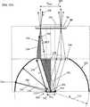
その出力角度が、さらに大きい角度の光が楕円の湾曲を有する直交する、金属のように反射する側壁の2つのセットにより遮られるように角度を変換する集光レンズの入力アパーチャを抜かす平面的なLED光源により発せられる光を収集し、再利用するための改善されたシステム及び方法を提供することが、本発明のさらなる他の目的である。各側壁の一方の焦線はLED光源アパーチャの平面内にあり、他方の焦線はLED光源アレイと集光レンズとの間に配置される実質的に透明なライトパイプの入力端縁にある。このライトパイプは、該ライトパイプから集光レンズの該入力アパーチャへと収集された光の一部を向けるようにする、光リダイレクト手段の分布に合わせられている。 A planar output lens that pulls out the input aperture of the converging lens that converts the angle so that the larger angle light is blocked by two sets of orthogonal, metal-like reflective sidewalls with elliptical curvature It is yet another object of the present invention to provide an improved system and method for collecting and reusing light emitted by LED light sources. One focal line of each side wall is in the plane of the LED light source aperture, and the other focal line is at the input edge of a substantially transparent light pipe disposed between the LED light source array and the condenser lens. The light pipe is tailored to a distribution of light redirecting means that directs a portion of the collected light from the light pipe to the input aperture of the condenser lens.
アレイの出力アパーチャ及びディスプレイの入力アパーチャに近接する位置にその前部焦点距離と後部焦点距離とが合わされた二次角度変換または集光素子によって、平面的な多層LEDビンアレイをLCDまたはDMDマイクロディスプレイに結合するための改善されたシステム及び方法を提供することが、本発明のさらなる目的である。 A planar multi-layer LED bin array can be transformed into an LCD or DMD microdisplay by a secondary angle transform or condensing element whose front and rear focal lengths are matched to the output aperture of the array and the input aperture of the display. It is a further object of the present invention to provide an improved system and method for coupling.
変換する素子のアパーチャにより収集されない全ての発せられた光を収集し、再利用するために設置される二次角度変換素子及び外部半球反射器によって、平面的なLEDアレイ光源をLCDまたはDMDマイクロディスプレイに結合するための改善されたシステム及び方法を提供することが、本発明のさらに追加の目的である。 A planar LED array light source can be transformed into an LCD or DMD microdisplay with a secondary angle conversion element and an external hemispherical reflector installed to collect and reuse all emitted light that is not collected by the aperture of the converting element It is yet a further object of the present invention to provide an improved system and method for coupling to a computer.
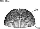
連続的な球面半径またはカットされた球面半径のいずれかを有する外部に設置される反射器によって、多層LED光源アレイから広角出力光を効率的に回収し、再循環し、再利用するためのコンパクトな手段を提供することが、本発明の1つの追加の目的である。 Compact for efficiently collecting, recirculating and reusing wide-angle output light from multi-layer LED light source arrays by externally mounted reflectors with either continuous spherical radius or cut spherical radius It is an additional object of the present invention to provide such means.
部分的に構造化された表面平面を有する隆起した透明なライトパイプと共に、外部に設置される四面の楕円形の反射器によって、多層LED光源アレイから広角出力光を効率的に回収し、再循環し、再利用するためのコンパクトな手段を提供することが、本発明の1つのさらなる追加の目的である。 Efficiently collects and recirculates wide-angle output light from a multi-layer LED light source array by an externally mounted four-sided elliptical reflector with a raised transparent light pipe with a partially structured surface plane However, it is a further additional object of the present invention to provide a compact means for reuse.
本質的には非散乱であるが、結果として生じる光線の角度方向をランダム化するのに役立つように金属のように反射するビンアレイの傾斜する側壁を形成するための改善されたシステム及び方法を提供することも、本発明のさらに追加の目的である。 Provide an improved system and method for forming slanted sidewalls of an array of bins that are essentially non-scattering but reflect like a metal to help randomize the angular orientation of the resulting rays This is also a further object of the present invention.
本質的には非散乱であるが、反射した光線の角度方向をランダム化するのに役立つように金属のように反射するビンアレイの一部の中にLED及び封入剤表面を形成するために改善されたシステム及び方法を提供することが、本発明の1つの他の目的である。 Improved to form LEDs and encapsulant surfaces in portions of the bin array that are essentially non-scattering but reflect like a metal to help randomize the angular orientation of the reflected rays. It is another object of the present invention to provide an improved system and method.
一方が角度変換素子の入力アパーチャと関連付けられ、他方が金属のように反射するLED光源アレイの出力アパーチャと関連付けられ、その金属のように反射する内部の焦点がLCDアパーチャの中心点または中心点の近くにある半球状の反射素子に結合される反射偏光子及び四分の一波長の位相遅延平面によって、直交偏光状態の光を再利用し、再利用する一方、LCDマイクロディスプレイ素子の入力アパーチャを通してLED光源システムから1つの偏光の光を効率的に透過させるための改善されたシステム及び方法を提供することが、本発明の追加の目的である。 One is associated with the input aperture of the angle conversion element, the other is associated with the output aperture of the LED light source array that reflects like a metal, and the internal focal point that reflects like the metal is the center point or center point of the LCD aperture. Reflective polarizers coupled to nearby hemispherical reflective elements and quarter-wave phase retardation planes reuse and reuse light in the orthogonal polarization state while passing through the input aperture of the LCD microdisplay element It is an additional object of the present invention to provide an improved system and method for efficiently transmitting one polarization of light from an LED light source system.
この層の上にあるいくつかの層は、その円柱軸がビンアレイの直交するアパーチャの対角線と、四分の一の波長の位相遅延層と、広帯域反射偏光層とに平行に位置合わせされる2つの直交する円柱レンズまたはレンズアレイを含む二次光配向層であるが、ある層は、その側壁湾曲がX経線(meridian)とY経線とのそれぞれにおいて入力アパーチャから出力アパーチャに伝送されるLEDのフラックス(flux:または束)を最大限にする、金属のように反射する4つの側面をもつビンの隣接するアレイである、高効率多層LED光源アレイを製造するための改善されたシステム及び方法を提供することが、本発明のもう1つの目的である。 Several layers above this layer are aligned parallel to the diagonal of the orthogonal aperture of the bin array, the quarter-wave phase retardation layer, and the broadband reflective polarizing layer. A secondary photo-alignment layer comprising two orthogonal cylindrical lenses or lens arrays, but one layer of an LED whose sidewall curvature is transmitted from the input aperture to the output aperture in the X and Y meridians respectively. An improved system and method for manufacturing a high-efficiency multilayer LED light source array that is a contiguous array of four side-reflecting bins like metal that maximizes flux. It is another object of the present invention to provide.
行及び列に配列される物理的に分離されたフリップチップLEDの一次元アレイまたは二次元アレイの電気的な結合及び相互接続を可能にする、電気導電性のある回路網のパターンを含むシリコン基板を製造するための改善されたシステム及び方法を提供することが、本発明のもう1つの目的である。 A silicon substrate comprising a pattern of electrically conductive circuitry that allows electrical coupling and interconnection of one-dimensional or two-dimensional arrays of physically separated flip-chip LEDs arranged in rows and columns It is another object of the present invention to provide an improved system and method for manufacturing.
その配列により、アレイ内の物理的なスルーホール(through-hole)が入力アパーチャと出力アパーチャとの両方を形成できるようにする、傾斜した側壁またはテーパ付きの側壁を有する金属のように反射するビンの一次元アレイまたは二次元アレイを製造するための改善されたシステム及び方法を提供することが、本発明の追加の目的である。関連付けられる入力アパーチャアレイは、対応するアレイの各LEDチップのサイズ及び形状に一致するように各入力アパーチャが空間的に配列されて1つになるときに、各LEDチップは、それにより各チップが各ビンへと突出する嵌合のように機械的な干渉を防止して、それぞれの対応する入力アパーチャを通じて同時に嵌合する。 The arrangement reflects a metal-like reflective bin with slanted or tapered sidewalls that allows physical through-holes in the array to form both input and output apertures. It is an additional object of the present invention to provide an improved system and method for manufacturing a one-dimensional or two-dimensional array. The associated input aperture array is such that when each input aperture is spatially arranged into one to match the size and shape of each LED chip in the corresponding array, each LED chip thereby causes each chip to be Mechanical interferences are prevented, such as fittings protruding into each bin, and they are simultaneously fitted through their corresponding input apertures.
隆起した偏光変換フィルム(elevated polarization converting film)と共に、関与する反射ビンの金属のように反射する性質及びLEDの電極の金属のように反射する性質を使用して、多層LED光源アレイから偏光されていない出力光を実質的に偏光された出力光に効率的に変換するためのコンパクトな手段を提供することも本発明の追加の目的である。 Along with the raised polarization converting film, it is polarized from the multi-layer LED light source array using the reflective nature of the reflective bins involved and the reflective nature of the LED electrodes. It is an additional object of the invention to provide a compact means for efficiently converting non-output light to substantially polarized output light.
本発明は、その構造上の詳細が、初期の多層パッケージング構造より優れており、相互接続された発光ダイオード(LED)のアレイからの光学出力を最大限にする多層パッケージング構造に関する。特に、本発明は、出力アパーチャの平方ミリメートルあたりの出力ルーメンが最高の集光度になるようにする。この改善は、ビデオ映写などの厳しい用途における電球の実用的な代替品としてのLEDアレイのできる限り早期の使用ができるようにする設計をもたらす。また、この改善は、本来の目的のために最小数のLEDを使用する関連設計ももたらす。 The present invention relates to a multilayer packaging structure whose structural details are superior to the initial multilayer packaging structure and maximizes the optical output from an array of interconnected light emitting diodes (LEDs). In particular, the present invention ensures that the output lumen per square millimeter of the output aperture has the highest concentration. This improvement results in a design that allows for the earliest possible use of LED arrays as a practical replacement for light bulbs in demanding applications such as video projection. This improvement also results in a related design that uses a minimum number of LEDs for the original purpose.
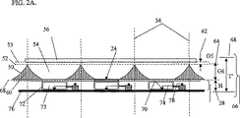
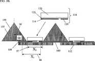
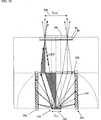
図1Aから図1Bの10や図2Aの66などの従来の発明では、例えば図1Aから図1Bのプリズムシート4および6や図2Aの反射偏光子56のように、ビンがそれらの真上に配置される一定の反射多層の設計と共に作用するように配列され、アレイ内の各LED(またはLEDのグループ)を取り囲んでいる、特別に形作られた特別なサイズの反射ビンの使い方を説明している。図1Aから図1Bの反射側壁2(及び22では)と図2Aの50の反射側壁2の形状とは、図1Aから図1BのLED20から反射多層(または図2A内の封入されたLEDエミッタ70)に向かって出力光を向け直すために調整される。そして、反射素子の間の複数の反射は、多岐に渡る照明用途のために有利な方法によりシステム10および66を通過する光の出力角分布を変えるために使用される。この多層手法は、LEDのアレイからの高密度出力光を達成するための基礎となるものの、アレイの出力密度を最大限にするための実用的な(working)関係はまだ確立されていない。 In conventional inventions such as 10 in FIGS. 1A to 1B and 66 in FIG. 2A, for example, the
図1Aから図1Bに紹介され、フリップチップLED20と共に示される形式では、平らなテーパ付きの側壁2のある浅い反射ビン12を使用する。LED光は、1個(または複数)のフリップチップLED20とメインビンのすぐ下に位置する封入剤14とを含むサブビン22からアパーチャ24を通ってビン12に入る。フリップチップLEDは、透明な基板層42と、その中にダイオードが形成されて光が発生するエピタキシャル素子層40とからなる。(反射率が高い表面下ミラーと結合される)電気接点44は、サブマウント24及び熱抽出層への取り付けができるようにする。形作られた反射側壁16と共にLEDチップを囲むサブビン22は、その基板42を通って、ビンアパーチャ24(及びオプションの拡散層8)を通って発せられるLED光を収集して伝達する。サブビン22及びメインビン12が連続エンティティとして形成され、共通の誘電体媒質18を共用し、同じ側壁傾斜度38(垂直面から測定される角度α)を有する図1Aから図1Bに、1つの特定の構成が示されている。 The format introduced in FIGS. 1A-1B and shown with
ビンから反射される光を角度分布と空間分布との両方により制御するように、その2枚のプリズムシート4及び6がLEDの好ましい高さG1’及びG1’+G4の上に持ち上げられた状態において、図1Aから図1Bの形式は機能する。追加の反射偏向子層28は、出力偏光も制御するために必要なときに追加される。プリズムが90度の頂角を有するように作られると、出力の優先順位36は、+/−22.5度内の角度に与えられる。ビーム均一性は、プリズムシート間隔の係数に依存する。 In a state where the two
図2Aから図2Cの類似した形式は、ビン側壁50の曲線状の形状により反射角制御プリズムシートの役割に代わる形式である。そのようにすることにより、ビンからの出力光は、ビンの上に持ち上げられた偏光子層56との反射相互作用によって角度及び偏光についてなおさらに厳しく制御される。 2A to 2C is an alternative form to the role of the reflection angle control prism sheet due to the curved shape of the
図1Aから図1Bと図2Aから図2Cとの両方の構造形式は、継ぎ目なく配列された出力アパーチャからの斜めに向けられた出力ビームを生じさせるが、どちらのシステムの(発せられた総LEDルーメンで除算された指定角度範囲内に入る出力ルーメンで表される)光学効率及び出力密度(アパーチャ面積で除算された指定角度範囲に入る出力ルーメン)も最大限にされていない。 Both structural forms of FIGS. 1A to 1B and 2A to 2C produce diagonally directed output beams from seamlessly aligned output apertures, but either system's (emitted total LED The optical efficiency and power density (represented by the output lumen falling within the specified angular range divided by the lumen) and the output density (output lumen falling within the specified angular range divided by the aperture area) are also not maximized.
LEDアレイ出力を最大限にすることの重要性は、(前部または後部)映写スクリーンに1000以上の白フィールドルーメンを送達することを必要とする現代のLCDまたはDMD(DLP)ビデオプロジェクタにより提示される困難な性能要件により説明できる。1つの共通RGB白フィールド分布は、緑が60%、赤が30%、青が10%であり、600緑スクリーンルーメン、300赤スクリーンルーメン、及び100青スクリーンルーメンを必要とする。プロジェクタは、そのそれぞれのアスペクト比が4:3でありその対角サイズのそれぞれが1.2”である、3つの反射LCDをf/2.4で使用すると仮定する。緑のチャネルとして、90%効率の映写レンズと81%の透過型二色性色分割立方体とを用いる限界の例とすると、+/−12度(つまりf/2.4)の角度範囲内の反射LCDに823.7偏光緑ルーメンがなければならないことに気付く。そして、前記に説明し、さらに詳細に後述される疑似ケーラー偏光ビームスプリッタ型角度変換器(pseudo-Kohler polarizing beam-splitter type angle-transformer)(25度から12度)を使用すると、関連付けられるLEDアレイ照明器が+/−25度内に1170偏光緑ルーメンを供給できなければならないことに気付く。+/−25度より大きい角度で生じた光は見ることができない。さらに、1170ルーメンのビームは、LCDの空間及び角度アパーチャに関係する根本的な幾何学方程式により定められる特定の矩形アパーチャ領域内に生成されなければならない(注記:正方形のアパーチャを使用することもでき、この変形はさらに後述する)。特に、そして周知の正弦関係から、照明アパーチャ端縁XILLとYILLは、方程式1および2に示されるとおりである。
従って、XLCDとYLCDとのそれぞれが24.384mmと18.288mmとであれば、LED照明器アパーチャは約12mm×9mmになる(さらに詳細な説明は後述する)。このアパーチャ領域の外に形成される光は、LCDアパーチャの範囲内に有効におさまることができない。したがって、十分な数の緑ルーメンがスクリーンに到達するためには、この特定の108−mm2照明アパーチャ領域内に1170の偏光緑ルーメンを生じさせることが実用的でなければならない。それらのルーメンは+/−25度に制限される。Therefore, if the XLCD and the YLCD are 24.384 mm and 18.288 mm, respectively, the LED illuminator aperture is about 12 mm × 9 mm (more detailed description will be described later). Light formed outside this aperture area cannot effectively fit within the LCD aperture. Thus, in order for a sufficient number of green lumens to reach the screen, it must be practical to produce 1170 polarized green lumens within this particular 108-mm2 illumination aperture area. Their lumens are limited to +/− 25 degrees.
このようにすることは、適切に効率的な高密度角度制御パッケージ内にLEDチップのアレイを配備することのない重大な課題に相当する。 Doing so represents a significant challenge without deploying an array of LED chips in a reasonably efficient high-density angle control package.
この問題の1つの表れとして、(Luxeon(商標)として)ルミレッズ(LumiLeds)により製造される最近の5ワット高出力LEDパッケージが、直径が約4mmである(後に示される)ドーム形の円形レンズから+/−90度のランベルト角分布(Lamvertian angular distribution)で120の偏光されていない緑ルーメンを発することを考える。当面、このような4mmのドームを閉じて詰めることができる(そして、それらはそれらの外部パッケージ用及び電極設計用には閉じて詰めることができない)ものと仮定すると、幾何学的配列から、実例となる9mm×12mmの照明矩形の中では合計7.5レンズドームという発光効果しか対応できないことが分かる。これらの7.5ドームは、必要とされる+/−25度ではなく、+/−90度の範囲内で偏光されていない900ルーメンを生じさせる。ルミレッズ(LumiLeds)は、公開されたデータシートの中で、このルミナスパワーの半分(450ルーメン)が+/−60度の範囲内に存在することを報告し、偏光されていない107ルーメンだけが+/−25度の範囲内にあることを暗示している。100%の偏光変換効率(約50%が実際的である)を可能にするとしても、このようなアレイは10倍以上プロジェクタニーズに及ばない。 One manifestation of this problem is that a recent 5 watt high power LED package manufactured by LumiLeds (as Luxeon ™) is from a dome-shaped circular lens that is approximately 4 mm in diameter (shown later). Consider emitting 120 unpolarized green lumens with a Lambertian angular distribution of +/− 90 degrees. Assuming that for the time being, such 4 mm domes can be closed and packed (and they cannot be closed and packed for their external packaging and electrode design), the geometrical example shows It can be seen that only the luminous effect of 7.5 lens dome in total can be accommodated in the 9 mm × 12 mm illumination rectangle. These 7.5 domes produce 900 lumens that are not polarized within the range of +/− 90 degrees, rather than the required +/− 25 degrees. LumiLeds reports in the published data sheet that half of this luminous power (450 lumens) is in the range of +/− 60 degrees, with only 107 unpolarized lumens + Implies to be within the range of -25 degrees. Even if 100% polarization conversion efficiency is possible (about 50% is practical), such an array does not meet projector needs more than 10 times.
このLuxeon(商標)パッケージ内においてルミレッズ(LumiLeds)により使用されるLEDチップは2mm×2mmの正方形である。パッケージがこのチップにより発生するルーメンを有効な出力に送る際にほぼ100%の効率であると仮定すると、5ワットのチップは1mm2あたり30ルーメンという密度で発光するであろう。電気的な効率が目的ではなかった(そしてそれは目的ではない)ならば、27もの数のこのようなスーパーチップが必要とされる12mm×9mmの照明アパーチャの中に適合し、+/−90度で偏光されていない3,240ルーメンを、または+/−60度で偏光されていない1,620ルーメンを生じさせることができるであろう。したがって、+/−25度の範囲内の歩留まりは、385.8未偏光ルーメンとなり、50%の変換効率の場合には、289.3偏光ルーメンとなるであろう。135ワットで動作するこのようなモンスターアレイも4倍プロジェクタの緑ルーメンのニーズに及ばない。The LED chip used by LumiLeds in this Luxeon ™ package is a 2 mm × 2 mm square. Assuming that the package is nearly 100% efficient in delivering the lumens generated by this chip to an effective output, a 5 watt chip will emit at a density of 30 lumens per mm2 . If electrical efficiency was not the goal (and it was not the goal), as many as 27 such superchips would fit in the required 12mm x 9mm illumination aperture and +/- 90 degrees It would be possible to produce 3,240 lumens that are not polarized at 1, or 1,620 lumens that are not polarized at +/− 60 degrees. Thus, a yield in the range of +/− 25 degrees would be 385.8 unpolarized lumen, and for 50% conversion efficiency would be 289.3 polarized lumen. Such a monster array operating at 135 watts does not even meet the needs of a 4X projector green lumen.
これらの同じ高出力フリップチップLEDの発光密度が現在1mm2あたり50ルーメンと同程度に高く、2004年までに、許容できる出力密度が2倍(または以下)で1mm2あたり100ルーメンのレベルに上昇することが証明されている。このような進展にも関わらず、いま説明されたモンスターアレイは270ワットで+/−90度で6,480未偏光緑ルーメンを生じさせるであろう。これは、ちょうど必要とされる数程度である1157の偏光緑ルーメンを生じさせるであろう。しかし、R−G−B用の総プロジェクタ電力が550ワットを超えて上昇していくため、このために必要なワット量は非現実的である。The emission density of these same high-power flip-chip LEDs is currently as high as 50 lumens per mm2 and by 2004, the allowable power density will double (or below) to 100 lumens per mm2 Proven to do. Despite such progress, the monster array just described will produce 6,480 unpolarized green lumens at 270 watts +/- 90 degrees. This will give rise to 1157 polarized green lumens, just as many as needed. However, since the total projector power for RGB is rising above 550 watts, the amount of watts required for this is impractical.
最高性能のLEDを用いてもなお必要とされているのは、このような従来の手段によって実現できるであろうものよりも、さらに斜めに効率的なLED照明アレイである。 What is still needed with the highest performance LEDs is an LED illumination array that is more diagonally efficient than would be possible by such conventional means.
3つの基本的な形式で示され、このニーズ及び関係するニーズに対処する本発明は、図1Aから図1B及び図2Bから図2Cに示される2つのオリジナル形式に基づいている。それぞれが、狭い角度範囲内及び限られた空間的な領域内に非常に多くの数のルーメンが必要とされることから、このような実用的な高ルーメン密度用途、特にビデオ映写をさらに促進にする。改善された形式は、商業的な優先順位が、最も少ない数のLEDを使用するときに可能なコスト削減を求める交通信号などの他の領域における実用的な用途も促進する。 Presented in three basic forms and addressing this and related needs, the present invention is based on the two original forms shown in FIGS. 1A-1B and 2B-2C. Each requires a very large number of lumens in a narrow angular range and in a limited spatial area, further promoting such practical high lumen density applications, especially video projection. To do. The improved format also facilitates practical applications in other areas, such as traffic signals, where commercial priorities seek cost savings possible when using the fewest number of LEDs.
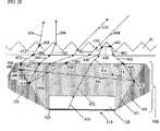
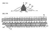
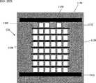
A.第1の形式:(図3Aから図3Bと図5Aから図5Cとのように)直線壁付きビン及び修正されたプリズムシートを使用する浅い外形(SHALLOW−PROFILE)の多層LEDアレイ
本発明の第1の形式は図3Aから図3Bに示され、浅い反射ビン82から構成される連続する規則正しいアレイ構造の使用を必要とし、平らな側壁106が、修正のある2枚の直交方向に向けられたプリズムシート88と92と、いわゆる四分の一の波長の位相遅延フィルム86と反射偏光子84とを含む、ビンアパーチャを覆う反射膜の縦の重なりのすぐ下に位置する。このコンパクトな形式、つまり図1Aから図1Bに示されている従来の形式の拡張は、システム90のバックプレーン94の上にLEDチップ118の最も密集した許容アレイを可能とすることにより最高のルーメン密度を達成する。LED自体のサイズに等しい、LED間の空の空間105を有するアレイの中にLEDチップを配置するよりもむしろ、この構造は、プリズムシート層88及び92の設計にその建設的な関係が依存するビンの側壁角度α38によって制限される、LEDのさらに密なパッキングを可能にする。A. First form: SHALLLOW-PROFILE multilayer LED array using straight walled bins and modified prism sheet (as in FIGS. 3A-3B and 5A-5C) One form is shown in FIGS. 3A-3B, which requires the use of a continuous regular array structure composed of shallow
さらに、LEDアレイと修正されたプリズムシートとの間の間隔は、最も下にあるプリズムシートとビン層自体との間の空隙によってではなく、浅い反射ビン82の深さにより設定される。このように、最適性能は、ビンとプリズム構造との間に存在する幾何学的な関係に依存する。 Further, the spacing between the LED array and the modified prism sheet is set by the depth of the
この構造において使用されるLEDは、任意の形または数でありうるが、(現在はサファイアである)透明な基板材料120が、その構造及び隣接する電極114及び116が発光を生じさせるp−n接合を形成するために作用する、(現在は窒化ガリウムベースである)エピタキシャル層122と結合されるいわゆるフリップチップ態様118により最良に製造される。電極114及び116は反射型に作られ、その結果、これらの素子に向けて発せられるあらゆる光は透明な基板層に向かって反射して、LEDから外側に反射する。 The LEDs used in this structure can be of any shape or number, but the transparent substrate material 120 (currently sapphire) is a pn that causes the structure and
その電極を下方に向けた状態でLEDチップを向けることの1つの特定の優位点とは、それにより電気的な相互接続を行う困難さが削減されるという点である。この場合では、LED電極の間に置かれるはんだ材料と、(バックプレーン94、または図3Aから図3Bの例に示されるように、サブマウント112のどちらかの)取り付け面に配置される反対に配置されるバー(つまりストライプ(stripe))100と108をリフローで接合するために、はんだ−バンピングとして知られるプロセスが最も良く使用される。フリップチップ向きのもう一つの優位点とは、それが熱発生源(電極とp−n接合)及びLED取り付けバックプレーン94に付着される熱抽出層96から最低の熱抵抗を提供するという点である。システムの正味の熱抵抗が、約150C未満の値に制限されなければならない運転中のその定常状態の温度を決定するため、または、材料障害からの重大な性能の劣化を危険にさらすため、全ての熱抵抗経路を最小限に抑えることは不可欠である。 One particular advantage of directing the LED chip with its electrodes facing down is that it reduces the difficulty of making electrical interconnections. In this case, the solder material placed between the LED electrodes and the opposite placed on the mounting surface (either of the
図3Aから図3Bに示される断面は、各ビン装置内の単一のLEDチップだけを表している。現代のLEDは、空気中で直接的に操作できるが、最高性能は実現可能なくらい高い屈折率(通常約1.49)の媒質内に封入101されるときに達成される。この誘電性の封入101の理由とは、全反射によってこの層の中、及び取り付けられた素子基板120内に保持できる発光層122内の光放射量を最小限に抑えることである。全反射のための臨界角が、光を含有する媒質とその周囲の間の屈折率の差異に依存していることは周知である。この差異が大きいほど、全反射により閉じ込められ、それにより適用されなくなる視感エネルギー(luminous energy:または光量)は多くなる。 The cross-section shown in FIGS. 3A-3B represents only a single LED chip in each bin device. Modern LEDs can be operated directly in the air, but the best performance is achieved when encapsulated 101 in a medium with a refractive index as high as possible (usually about 1.49). The reason for this
図3Aから図3Bのビン構造の幾何学的な形式は、図1Aから図1Bの下部のように、同じ側壁角度α、38、及び同じ内部誘電体媒質18を有するように作られたサブビン層12及びメインビン層12付きの我々の従来の発明に説明されたビン構造の特別なケースである。ビン構造126は、図4Aから図4Bに概略して示されるように、形成されるアレイ構造126の陰の(つまり逆の)形状に形成された機械設備128を使用して製造される。示されている対称的な(正方形)のビンの場合には、型ツール128は、例えば、特別に成形されたダイヤモンド工具を使用して繰り返し罫線をプランジカットすることにより母材基板から図4Bのように製造され、最終的な総グルーブ角度が2αとなるように成形され、αは図3Aから図3Bに示されるように側壁角度38である。単一点切削またはフライカッティングなどの他の等しく安定した切削方法も使用されてよい。いったん適切に成形された型ツールが作成されると、それは、電鋳、成形、エンボシング、及び鋳造及び硬化などの多くの安定した成形プロセスの内の任意の1つのマスタとして使用され、結果として図4Aに示されるようにパーツ126が形成される。型ツールのメサ135は、結果として生じるパーツ126に清潔で遮るもののないスルーホールが作られることを保証し、鋳造、成形またはエンボシングの製品を打ち抜くことができるようにするために、わずかに引き延ばされてよい。 The geometrical form of the bin structure of FIGS. 3A-3B is a sub-bin layer made to have the same sidewall angle α, 38 and the same
図4のガイドライン130は、図4A内の成形されたパーツ126の一部が図4B内の型ツール128内の溝付きのパターンの一部からどのようにして取れるのかを示す。例えば、化学エッチング、放電機械加工、及び実際のビンサイズによっては、ワイヤ放電機械加工などの任意の適切な直接成形方法によりビンパーツ126を形成することは等しく実現可能である。これらのうち、金属などの導電材料を形成するという優位点は、システムの熱抽出能力を増大させ、構造の全体を通ってその下にある熱抽出層6(図3Aから図3B)に熱を拡散するという点である。ビンパーツ126が金属により成形されるのか、またはプラスチックにより成形されるのかに関係なく、その側壁表面は、以後(または同時に)保護金属または強化アルミニウムなどの高反射率の鏡面反射膜でコーティングされる。 The
フリップチップLED118が図3Aから図3Bの個々のサブマウント112上でそれらの製造メーカによって事前に取り付けられるケースでは、ビンパーツの下面は、後述されるように、関連付けられた電気相互接続ストライプ100と108のための基板として便利に使用される。 In the case where the
ビンパーツ126は、126などの物理的な構造の内部空洞内を普通に充填する誘電性のカプセル化ビン構造101を機械的に支えるための技術でありうる。この場合、反射側壁は金属によってではなく、結合されていない誘電体と金属面の間の空気の薄い層によって境界が付けられる誘電体構造の内部側壁になる。この誘電体構造の物理的な形状は、直接的に型ツール128の物理的な形状を模倣し、主要な違いはそれが、代わりにコーティングされていない光学的にクリアで(clear)透明な誘電材料から作られているという点である。誘電性の金属境界よりむしろ、このような誘電性の空気境界から反射する光のための従来の優位点とは、全反射(total internal reflection:以下、「TIR」とよぶ)を行う際に達成される反射率が純粋に金属性の反射の反射率よりかなり高いという点である。しかしながら、誘電体反射構造の改善された反射率によりなされる、相殺する利得は、TIRをあきらめ、誘電体を空気の中に逃がす光線の損失である。これらの損失は、回避されない場合には、全ての光線を処理する金属性の反射壁106を使用するための優先を生じさせるであろう。このような損失を回避する1つの方法は、(図4Aにおいて126として成形される)反射ビン構造の使用を(図4Bにおいて128として成形される)誘電性インサートに結合することである。これが行われると、LEDチップから誘電体の中に結合される全ての光は、直接的に、または切り離された金属反射面から空気ギャップ全体に外部反射によって、ビンの出力アパーチャXi(98)を通じて誘電体101に通される。この手法をとる唯一の欠点は、誘電性媒質101の中にLEDチップを浸漬しなければならないという点である。これは、物理的なビン126(図4A)をシリコーンなどの弾性絶縁材で充填するときには簡単であるが、LEDチップを前もって形成された誘電材料の中に侵入させるときにはあまり簡単ではない。この手法に対処する1つの方法は、成形ツールの中に小型のチップサイズ・ボス(chip-sized-boss)を前もって形成し、その結果それが成形された誘電体内にチップサイズのウェルを生じさせるであろう。それから、チップと誘電体との間に光学接点を作るために光接着剤が使用されるであろう。The
本発明の主な改善策は、そのより現実的なフリップチップLED取り付け構造及びその浅いビン構造の他に、図5Aから図5Cにさらに詳細に示される2枚の隆起したプリズムシート88及び92の構造及び位置にある。 The main improvement of the present invention is that in addition to its more realistic flip chip LED mounting structure and its shallow bin structure, two raised
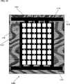
B.ビンの深さ及び改良されたプリズムシート
図5Aから図5Bのように、新しい発明においては、ビン深さG1、102は、(図5Cに別にも示されるような)プリズムシート88及び92とLEDアレイの発光面との間に最善の隙間を設定するために使用される。従来の発明では、下部プリズムシートとLEDアレイとの間の隙間はビン深さによってだけではなく、プリズムシート基板とビン層の上部との間の物理的な間隔によっても設定された。B. Bin Depth and Improved Prism Sheet As in FIGS. 5A-5B, in the new invention, the bin depths G1, 102 include
任意のビンの深さは、アレイの有効出力ルーメンを大きく制限してよいことが分かる。 It can be seen that any bin depth may greatly limit the effective output lumen of the array.
プリズムシート自体も、図5Aから図5Cのように改良されていてもよく、その結果それらの頂角β1+β2(138と140)が下にある浅いビン層82との反射相互作用を最適化するが、一定のケースでは、基板層161は、例えば正のまたは負の円柱レンチキュラレンズ構造のために改変されていてもよい。このような任意選択的な拡散構造を含むことは、全体的なビーム均一性に対するそれらの有利な影響が所望されるときに保証される。The prism sheet itself may also be modified as shown in FIGS. 5A to 5C, so that the reflection interaction with the
もとの発明では、2枚の直交方向に向けられるプリズムシート(図1Aから図1Bの4と6を参照すること)は、3Mの商業上の輝度強化フィルム(BEF(商標))に類似する、それ以外の場合平面的な基板上で平行した90度のプリズム溝を使用する。3Mの90度BEFプリズムシートは、(ラップトップコンピュータ及びデスクトップモニタで使用されるもののような)フラットパネルLCD画面での視認輝度を増すために使用される。パッシブフラットパネルバックライトを背にして直接的に、及び照明されるLCD画面のすぐ後ろに配置されるBEFとは異なり、本プリズムシートは、図1Aから図1Bのように、光源(つまりビンに入れられたLEDアレイ)に関して、及び互いに関して、それぞれ特定の距離持ち上げられる。シートの上昇は、出力アパーチャの全域でLEDアレイにより生成される照明ビームの全体的な空間均一性を改善する目的で、シートのそばに生じる各LEDの発光領域の4つの仮想画像のために最善の位置を達成するために使用される。 In the original invention, two orthogonally oriented prism sheets (see 4 and 6 in FIGS. 1A-1B) are similar to 3M commercial brightness enhancement film (BEF ™). Otherwise, parallel 90 degree prism grooves on a planar substrate are used. The
目標が、(例えば、上記ビデオプロジェクタ例によって必要とされる+/−25度のように)所与の角度範囲内において反射型でビンに入れられたLEDアレイから結合される光のビームの中で総出力ルーメン数を最大限にするものであるときでも、光源の上に任意に配置される(平らな基板及びその頂角が90度であるプリズム溝を使用する)従来のプリズムシートは、最高性能を生じさせない。 The target is in a beam of light that is combined from a reflective and binned LED array within a given angular range (eg, +/− 25 degrees as required by the video projector example above). The conventional prism sheet (using a flat substrate and a prism groove whose apex angle is 90 degrees) arbitrarily disposed on the light source even when the total output lumen number is maximized at Does not give maximum performance.
その前面(図5A)及び側面(図5B)の断面という点から見て、図5Aから図5Cと、2枚の改良されたプリズムシートの斜視図(図5C)とに好ましい構造が示されている。好ましい構成では、ビン層82は、深さG1、102及び垂直面γ、39から測定された側壁角度を有し、それらの関係性は、方程式(3)でのように、(前面図及び側面図の)各経線においてLEDチップ118のサイズXcである97と、ビン底部Xi100の相対的なサイズと、ビンの出力アパーチャXoである98とによって決定される。最適値は、ビン幾何学的配列と改良されたプリズムシート上部構造の幾何学的配列の間の反射相互作用の特定の性質に依存するが、アレイ内でLEDの密度(及び数)を最初に確立するのは、ビンの出力アパーチャであるX0のサイズである。入力アパーチャに対する出力アパーチャの比(X0/Xi)が大きいほどアレイはまばらになり、入力アパーチャに対する出力アパーチャの比が小さいほどアレイは密になる。
経線(XまたはY):
Meridian (X or Y):
1Dアレイ及び2Dアレイには今日のLEDを配列する密度に対する実用的な制限があり、コスト及び総サポート可能ワット量によって主に動かされる。さらに詳細に後述されるように、平方ミリメートルあたりに必要とされるLEDワット量が高いほど、熱抽出のタスクは難しくなる。 1D arrays and 2D arrays have practical limits on the density of today's LED arrays and are driven primarily by cost and total supportable wattage. As will be described in more detail below, the higher the LED wattage required per square millimeter, the more difficult the heat extraction task.
改良されたプリズムシートは、角度β1である138と角度β2である140との合計である、曲率半径Rのプリズム頂角と、正または負の円柱レンズ状構造(positive or negative cylindrical lenticular lens)を任意選択的に含む基板層とからなる。それらを含む各シートでは、円柱レンズ軸が対応するプリズム溝の軸に実質的に平行に通る。(図5Cのように、下部シート92内の141と上部シート88内の143との)プリズムシート対角線は、好ましくは互いに対して直交方向に位置合わせされるが、図4Aのようにビンアパーチャ対角線129及び131に対する任意の角度向きに位置合わせされていてもよい。The improved prism sheet has a prism apex angle of radius of curvature R, which is the sum of angle β1 138 and
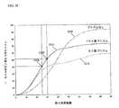
C.最適化の方法
完全にパラメータ化された予測コンピュータモデルが、ビンアレイ幾何学的配列とプリズムシートの幾何学的配列との間の性能に対する根本的な影響を探索するように構築される。従来の研究室実験ではなく、この目的に予測モデルを使用することの優位点は、柔軟性、時間効率、及びコストである。ビンアレイの幾何学的配列とマイクロプリズムシートの幾何学的配列との十分に多様な組み合わせのものを製造することは、かなり大きな費用がかかる課題であろう。コストが対象でないとしても、幾何学的な変数を探索できる適合性の度合いに対して実際的な制限があろう。C. Method of Optimization A fully parameterized predictive computer model is constructed to explore the fundamental impact on performance between the bin array geometry and the prism sheet geometry. The advantages of using predictive models for this purpose, rather than traditional laboratory experiments, are flexibility, time efficiency, and cost. Producing a sufficiently diverse combination of bin array geometry and microprism sheet geometry would be a rather expensive task. Even if the cost is not the target, there may be a practical limit to the degree of suitability with which geometric variables can be searched.
方程式3の幾何学的な配列関係の他に、方程式3のパラメータと、プリズムシートパラメータ、つまり、下部シートの場合β1とβ2、下部シートの場合R、上部シートの場合β1とβ2、上部シートの場合R、G2とG4との間で同等に簡単な数学的関係を引き出すことはできない。各界面での反射と透過の機構は十分に理解され、金属性界面と誘電性界面との反射及び屈折の法則だけに基づいているが、数学的な複雑さは、図5Aから図5Cの平面の内部と外部との両方(つまり近軸光線及びスキュー光線)を移動する、多数の幾何学的な光線の集合的な挙動を定量化する必要性から生じる。この必要性は、従来、その原値からそれらの目的地の点に多数の無作為に生成された光線の経路に従う光線トレースプログラムによって対処される。In addition to the geometrical arrangement of equation 3, the parameters of equation 3 and the prism sheet parameters, ie, β1 and β2 for the lower sheet, R for the lower sheet, β1 and β2 for the upper sheet. In the case of the upper sheet, it is not possible to draw an equally simple mathematical relationship between R, G2 and G4. The mechanism of reflection and transmission at each interface is well understood and is based solely on the laws of reflection and refraction between metallic and dielectric interfaces, but the mathematical complexity is the plane of FIGS. 5A-5C. Arises from the need to quantify the collective behavior of a large number of geometrical rays moving both inside and outside (ie paraxial and skew rays). This need is traditionally addressed by ray tracing programs that follow a number of randomly generated ray paths from their original values to their destination points.
このような手法は、図5Aから図5Bに提供される断面詳細を条件に、図3Aから図3Bのシステム90について取られた。複雑な光学システム、特に反射プロセスと屈折プロセスと吸収プロセスとだけがある光学システムの光線軌跡の有効な法則は、この目的のために製造された商業的な光線トレースソフトウェア製品のほぼいずれかにより確信的に確実に表される。現在の作業は、ASAP(商標)7.0、アリゾナ州タクソン(Tucson、Arizona)にあるBreault研究組織の製品を使用して簡単な方法により実行された。 Such an approach was taken for the
計算精度は、主に、光線のソースが表される実在論(realism)に依存しており、この場合のソースは現代のフリップチップLEDである必要がある。とはいえ、図3Aから図3Bのシステム90は、実際には非イメージング光学システムであるため、必要とされる以上にLED自体の正確なデバイス内部の物理学についてのさらに詳しい表現から恩恵を受けない。必要なのは、LEDの最も重大な構造上の機構の十分な光学表現を示すために使用されるフリップチップ型LEDの適度な幾何学的な配置だけである。 The calculation accuracy depends mainly on the realism in which the source of the light is represented, and in this case the source needs to be a modern flip chip LED. Nonetheless, because the
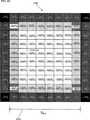
我々が使用したフリップチップLEDソースモデルの詳細な説明は、図3Aから図3Bに象徴される一般化されたフリップチップ断面の後に、図6Aから図6Cに提供されている。このモデルは、ルミレッズ(LumiLeds)によって現在製造されている高出力緑及び青の窒化ガリウムオンサファイアLEDの適度な表現となることを意図されている。ルミレッド(LumiLeds)のLEDは、鏡として働く図6Bに表されている新規の(そして高反射率の)相互に分離された(inter−digitated)電極構造125(125A及び125B)を特徴とする。それは実際には素子アパーチャ全体を覆うため、この鏡の構造を忠実に近似する試みはなされなかった。窒化ガリウムエピタキシャル層122(屈折率約2.4)は、光線が平面内で及び考えられるあらゆる角度方向で無作為に空間的に生成される発光面123の近似位置を示すために122Aと122Bとして分割される。サファイア基板(屈折率約1.8)は、厚さ約100ミクロンである。エピタキシャル層122内に生成される多くの光線は、高屈折率の波長内に閉じ込められたままである。エピタキシャル層を逃れる光線は、それらの境界端縁またはサファイア基板120の界面のいずれかを通して逃れる。同様に、サファイア基板内の全反射を逃れる光線は、5つの露呈したサファイア面を通る出力として逃れる。 A detailed description of the flip chip LED source model we used is provided in FIGS. 6A-6C after the generalized flip chip cross section symbolized in FIGS. 3A-3B. This model is intended to be a reasonable representation of the high power green and blue gallium nitride on sapphire LEDs currently manufactured by LumiLeds. LumiReds LEDs feature a novel (and high reflectivity) inter-digitated electrode structure 125 (125A and 125B) represented in FIG. 6B that acts as a mirror. Since it actually covers the entire element aperture, no attempt has been made to faithfully approximate the structure of this mirror. The gallium nitride epitaxial layer 122 (with a refractive index of about 2.4) is used as 122A and 122B to show the approximate location of the
図3Aから図3Bと、図5Aから図5Cのように、フリップチップLED118を取り囲む(封入する)屈折率は、通常、約1.49である。ソースモデルは、露出する素子について報告される(または期待される)実験結果に対して、事前に校正される。校正変数は、(約2ミクロンであるとして解釈される)エピタキシャル層122のミクロン単位の厚さ、(約0.89であると解釈される)電極鏡125の反射率と、素子のシミュレーションされたp−nジャンクション平面123内で実際に生じる、1平方ミリメートルあたりの平均ルーメン(lumen/mm2)とを含む。校正は、総ルーメンの全ての出力光線を収集、分析することと、この結果を実験において観察された結果と比較することとによりなされる。モデル値及び実験値が一致するまで、性能制御変数のいずれかに対して賢明な(judicious)変更が加えられる。この特定のケースでは、変数が実際にそれらの物理的な現実を表すことは、それらがLEDの総出力ルーメンの正しいシミュレーションを可能とするために結合するより重要ではない。As shown in FIGS. 3A to 3B and FIGS. 5A to 5C, the refractive index surrounding (encapsulating) the
いったんLEDソースは確実に校正されると、それは、システムの出力予測がまさに正確及び現実的であることが判明するという自信をもって、図3Aから図3Bの完全な照明システム90内に組み込まれる。 Once the LED source is reliably calibrated, it is incorporated into the
D.幾何学的な関係性及びそれらのLED照明器性能に対する影響
必要とされる角度範囲内に含まれる出力ルーメンの総数がLED照明器性能を規定する。D. Geometric relationships and their impact on LED illuminator performance The total number of output lumens included within the required angular range defines the LED illuminator performance.
図3Aから図3Bの照明システム90の一例として、我々は前述されたLEDソースモデルと、1mm2あたり100ルーメン(2005年前半までの最高性能のルミレッズ(LumiLeds)生産装置から予測される性能)を生じさせることができる1平方ミリメータあたりのルミレッズ(LumiLeds)型フリップチップLED118のアレイのケースを使用する。As an example of the
前記したプロジェクタの例に一致するアレイのアパーチャは、12mm×9mmの矩形(または12mm×12mmの正方形)の断面と、名目上+/−25度の有効照明角度とにほぼ制限される。このアレイで使用されるLED数は、コスト及びワット量を制御するために約40〜50チップに制限される。つまり、正方形のビンアパーチャの場合には、X0は1.6mm(つまり(12)(9)/(1.6)2)=42、または(122)/(1.62)=56)である。LEDチップの回りのビンの底部での小さなマージンを見越すと、Xiは1.1mmとなり、ビンの側壁角度αは、方程式3により決定される(図3Aから図3Bの)ビン深さG1、102の幾何学関数となる。The array aperture, consistent with the projector example described above, is almost limited to a 12 mm × 9 mm rectangular (or 12 mm × 12 mm square) cross-section and an effective illumination angle of nominally +/− 25 degrees. The number of LEDs used in this array is limited to about 40-50 chips to control cost and wattage. That is, in the case of a square bin aperture, X0 is 1.6 mm (ie (12) (9) / (1.6)2 ) = 42 or (122) / (1.62) = 56). is there. In anticipation of a small margin at the bottom of the bin around the LED chip, Xi is 1.1 mm, and the bin sidewall angle α is determined by equation 3 (shown in FIGS. 3A-3B), the bin depth G1, 102 geometric functions.
他の構成変数は図5Aから図5Bにより明確に示され、下部プリズムシート隙間間隔G2、132、下部プリズムシートレンズ半径RL、144、下部プリズムシート頂角β1+β2、(下部シートの上部を基準とした)上部プリズムシート隙間隔G4、31、上部プリズムシートレンズ半径RH、142、及び下部プリズムシート頂角β1+β2を含む。簡単にするために、四分の一波長層86及び反射偏光子層84は分析に含まれていない。The other constituent variables are clearly shown in FIG. 5A to FIG. 5B, and the lower prism sheet gap spacing G2, 132, the lower prism sheet lens radius RL , 144, the lower prism sheet apex angle β1 + β2 , (the upper part of the lower sheet The upper prism sheet gap gaps G4, 31, the upper prism sheet lens radius RH , 142, and the lower prism sheet apex angle β1 + β2 . For simplicity, the
プリズムシート基板層161の上にレンズ構造142または144を含み、有効出力ルーメン、空間ビーム均一性、またはその両方が改善されるいくつかの場合がある。 There may be some cases where a
全ての出力光線は上部プリズムシート88の先端の点の上にじかに配置される大きな吸収面上で収集される。全ての角度(+/−90度)での総フラックスはシステム90の全体的な収集及び透過効率を反映する。+/−25度という角度範囲内に検出されるフラックス断片は、より詳細に進展されるように、ビデオプロジェクタ応用例の長所の重大な基準と、最大限にされる性能インジケータとである。 All output rays are collected on a large absorbing surface that is placed directly over the point at the tip of the
説明される1.6mmビン内での1mmのLEDチップの最善の結果は、174ミクロンビン深さと、対称的な52度プリズム頂角αとにより達成される。 The best results for a 1 mm LED chip within the 1.6 mm bin described are achieved with a 174 micron bin depth and a symmetrical 52 degree prism apex angle α.
この独特な設計組み合わせの開発は、以下の分析から生じる。 The development of this unique design combination results from the following analysis.
E.ビン深さ及びプリズム角度の影響
優良LEDアレイ照明器は、完全(LCDまたはDMD)視野カバレージ(この場合では+/−25度)を達成するために必要とされる角度範囲内の出力ルーメンの最高数を生じさせ、LEDアレイアパーチャ上で均一に生じさせる。この挙動は、図5Aから図5Bのようにプリズムシート88及び92の中にあるプリズムの、反射ビン深さ102、G1と完全頂角β1+β2との間の協調関係に依存している。E. Bin Depth and Prismatic Angle Effects A good LED array illuminator is the highest in output lumen within the angular range needed to achieve full (LCD or DMD) field of view coverage (in this case +/− 25 degrees). The number is generated and generated uniformly on the LED array aperture. This behavior depends on the cooperative relationship between the
最大可能出力性能を達成するときのビン深さ102の重要性は、図7の3つの特定のまっすぐな壁の場合または平らな壁のケースについて確認される。すなわち、ビンだけ(曲線141)の場合と、ビンと業務用の輝度強化フィルムBEFシート(曲線143)の場合と、ビンと特別に最適化されたプリズムルーメン強化フィルムLEFの交差したシート(曲線145)の場合である。 The importance of
ビンに入れられたフリップチップLED単独のケースでは、チップ厚さ自体よりわずかに深いだけである135ミクロンというビン深さでアレイについて約1000ルーメンのわずかな出力ピークがある(図7の曲線168を参照のこと)。後述されるように、このピーク性能に対応するビン深さは、理想的に成形された曲線状の壁の非イメージング光学集光器ビンを厳密に近似する。 In the case of a flip-chip LED alone in the bin, there is a slight output peak of about 1000 lumens for the array at a bin depth of 135 microns, which is only slightly deeper than the chip thickness itself (see
2枚の業務用のプリズムシートが、それぞれ90度の頂角を備え、プリズム溝が互いに垂直に通るビン付きLEDの上にじかに追加されると、出力ピークは約1280ルーメンまで28%上昇し、対応するビン深さは約174ミクロンまで増加する(図7の曲線170を参照のこと)。この結果は、重大な設計要因としてのビン深さの重要性を強調している。プリズムシートが135ミクロンの深さのビンの上に使用されるときには性能利得はほとんど、またはまったく見られない。しかし、同じプリズムシートが174ミクロンのビンの上に使用されると、見かけの利得は60%である。したがって、ビンに入れられたLEDチップの上にプリズムシートがじかに配置された状態での意味のある有効ルーメン利得の場合には、ビン深さは任意に選ばれてはならない。 When two commercial prism sheets are added directly on top of a bottled LED, each with a 90 degree apex angle and the prism grooves running perpendicular to each other, the output peak increases by 28% to about 1280 lumens, The corresponding bin depth increases to about 174 microns (see
通常、BEF(ときにはVikuiti(商標)BEF 90/50)と呼ばれる90度のプリズムシートは、全ての直視型LCDディスプレイ画面に共通する蛍光バックライトにおいて輝度強化のために使用される、3Mによって製造販売されているプラスチックフィルム製品である。90度のプリズムは直視型ディスプレイの見かけの輝度を増加するためには最善でありうるが、90度はLEDアレイ照明器の出力ビーム内の有効ルーメン数を強化するために最善の頂角であることは判明していない(図7の曲線172を参照のこと)。この場合には、頂角は、下部プリズムシートと上部プリズムシートとの両方について104度の全角度まで増加される。これが行われると、総有効ルーメンは、ちょうど174ミクロンとほぼ同じビン深さの1580までさらに23%上昇する(図7の曲線172を参照すること)。 A 90 degree prism sheet, usually called BEF (sometimes
BEFは、通常、高度に散乱する白空洞(white cavity)と共に使用される。ここで、開発された最適の104度のプリズムシートは、その反射面が高い鏡面反射率をもつビンアレイと共に使用するために開発される。 BEF is typically used with a highly scattering white cavity. Here, the optimal 104 degree prism sheet developed is developed for use with a bin array whose reflective surface has a high specular reflectance.
ビン深さ102とプリズムシート頂角138及び140との間に存在する詳細な物理的な関係性は、ビン側壁106とLEDのフリップチップの内部構造118とプリズム切子面自体との間の複数の3次元反射を必要とする非常に複雑なものである。 The detailed physical relationship that exists between the
134um、154um、174um、204um及び234umというビン深さについてこの関係性の基本的な(net)影響を要約する1つの方法が、総有効ルーメンが、下部シート及び上部シートについて等しくされている完全プリズム頂角の関数として描かれる図8に示されている。この場合では、ピーク性能は、より従来の90度、178ではなく106度、176を通して100度の近傍で発生することが判明しており、174um、180の近傍でのビン深さに強い好みが見られる。ビン深さが大きくなると、1.6mm、側壁角度150、γで一定に保持されるビンアパーチャは、総有効ルーメン数が減少するように減少する。ビン深さが減少すると、側壁角度は大きくなり、有効ルーメン数も減少する。 One way to summarize the net effect of this relationship for bin depths of 134um, 154um, 174um, 204um and 234um is a complete prism where the total effective lumen is equal for the lower and upper sheets It is shown in FIG. 8 drawn as a function of the apex angle. In this case, the peak performance has been found to occur in the vicinity of 100 degrees through 106 degrees and 176 rather than the conventional 90 degrees and 178, and there is a strong preference for bin depths near 174 um and 180 degrees. It can be seen. As the bin depth increases, the bin aperture held constant at 1.6 mm,
174umビン深さについて図8において発生する総有効ルーメンのピークは、図9の94度と109度との間の一連のプリズム頂角にわたってさらに綿密に調べられる。図9に示される各データポイント(白抜き正方形)は、少なくとも500,000光線のコンピュータ光線トレースランを表す。小さな変動にも関わらず、この挙動は、上部プリズム角度と下部プリズム角度とが、100度と106度との全角度176の間になる図5の構造のための相対的な性能安定性の領域を示唆する。性能ピークは、約102度(180)と106度(181)との間に見出される。 The total effective lumen peak occurring in FIG. 8 for the 174 um bin depth is examined more closely over the series of prism apex angles between 94 and 109 degrees in FIG. Each data point (open square) shown in FIG. 9 represents a computer ray trace run of at least 500,000 rays. Despite small variations, this behavior is a region of relative performance stability for the structure of FIG. 5 in which the upper and lower prism angles are between the
この重要な物理的な関係性を示すさらに別の方法は、やはり実例となる1.6mmビンアパーチャについて図1Aから図1Bに示されている。総有効ルーメンは、ローエンドでの従来の90度全角度プリズムからハイエンドでの106度プリズムへ、種々のプリズム頂角のためのビン深さの関数として描かれる。プリズムシート頂角の全てのケースにおいて、好ましいビン深さは、160〜180ミクロンである182の範囲内にあることが分かる。 Yet another way of showing this important physical relationship is shown in FIGS. 1A-1B for an illustrative 1.6 mm bin aperture. The total effective lumen is plotted as a function of bin depth for various prism apex angles, from a conventional 90 degree full angle prism at the low end to a 106 degree prism at the high end. It can be seen that in all cases of prism sheet apex angle the preferred bin depth is in the range of 182 which is 160-180 microns.
F.多層ビンプリズムシート構成の独自性
従来のレンズベースの収集光学より優れる図3Aから図3B及び図5Aから図5CのこのLED照明器発明の独自性は、前述されたプロジェクタの例との関連により評価できる。1つの例として、12mm×9mmの40LEDアレイからの光が、出力光が+/−12℃についてプロジェクタのニーズを満たすように従来のレンズにより収集されてから、中継されると仮定する。この場合には、使用されるレンズは、約+/−25度でのみアレイから有効光を収集するであろう。40個のLEDは、全ての角度にわたって均等に拡散される4,000ルーメンを生成するであろうが、714ルーメン[(4000Sin2(25))だけが+/−25度の範囲内に含まれるであろう。したがって、本発明において一意の寸法のビン(134ミクロンと174ミクロン、図7)を使用することによる利得は、この性能を40%以上超えるであろう。本発明において一意の寸法のビンを従来の90度プリズムシートと共に使用することによる利得は70%以上であろう。そして、本発明において一意のサイズのビンを対応する最適化された102度から106度のルーメン強化プリズムシートと共に使用するための利得は100%以上(つまり2x)であろう。F. Uniqueness of the multi-layer bin prism sheet configuration The uniqueness of the LED illuminator invention of FIGS. 3A-3B and 5A-5C, which is superior to conventional lens-based collection optics, is evaluated in connection with the projector example described above. it can. As one example, assume that light from a 12 mm × 9
ビンアレイ−プリズムシート組み合わせの独特な性能は、第2.2.6.2項でなおさらに徹底的に探索される。 The unique performance of the bin array-prism sheet combination is explored even more thoroughly in Section 2.2.6.2.
G.プリズムシート構造及び他の改良の効果
複数の構造上の変形物を、基本的なプリズムシート88及び92(図3Aから図3B及び図5Aから5C)に加えてもよい。1つの変形物は、球状または非球面の湾曲を、下部プリズムシート92、上部プリズムシート88、または両方の上のプリズム切子面(図5Aから図5Cの89)自体に追加することを必要とする。第2の変形物は、光表面構造142及び144を、上部プリズムシート基板及び下部プリズムシート基板161に追加することを必要とし、この構造は構造深さ160(下部シート92)または164(上部シート88)のプリズム切子面または円柱状レンズのどちらかである。しかしながら、単独にまたは組み合わされて含まれる、これらの追加のいずれも、総有効ルーメンに好ましい効果を与えることは判明していない。1つの例外がある。球状の円柱レンズ142及び144をプリズムシート基板に追加することは、ビーム均一性の処理において後述されるようにビームの全体的な空間均一性を改善することが判明している。G. Effect of Prism Sheet Structure and Other Improvements Several structural variations may be added to the
H.偏光再利用の有益な効果
本発明の中に含まれるいくつかの考えられる偏光再利用と変換の機構の内の1つが図11に描かれている。より大きなアレイの中の単独のLEDアレイ要素だけが明確にするために示される。この場合では、図5Aから図5Cのようなプリズムシート159のセット(第1のプリズムシート92及び第2のプリズムシート88)と四分の一波長の位相遅延層86と反射偏光層84とを含むフィルムスタックの下に、フリップチップLED118を含む浅いテーパ付きの側壁116反射ビン82を描く。この例では、反射偏光層84及び位相遅延層86は、図11に示されるようにプリズムシート159の下か、またはそれらの上に置かれてもよい。最善の配列は、使用される材料の物理特性に依存する。H. Beneficial Effects of Polarization Reuse One of several possible polarization reuse and conversion mechanisms included in the present invention is depicted in FIG. Only a single LED array element in a larger array is shown for clarity. In this case, a set of prism sheets 159 (
一般的には、最も効率的な偏光変換は、偏光層84及び86が金属性の反射ビンの真上とプリズムシート159の真下とに配置されるときに予測される。この配列を使用すると、プリズムシート159は、以後の偏光解消を引き起こさないように不均一な応力を受けない非複屈折材料から作られなければならない。偏光層をプリズムシートに配置すると、偏光解消の可能性を最小限に抑えるが、場合によっては、利得が増加される前に必要な再利用の数を増加する。角度及び偏光(angular and polarization)の成功に必要な収集再利用が多いほど、収集吸収及び散乱からの光線から失われる出力は多くなる。 In general, the most efficient polarization conversion is expected when the
偏光回収機構は、偏光変換層がプリズムシートの上にある後者の場合のための実例となる多くの考えられる光線経路の内の2つに従うことによって説明される。任意の光線セグメントの偏光は図11の底部にある偏光キーに要約され、3本の平行する線が偏光されていない光線を表し、単一破線が線形s−偏光を表し、二重破線が左側の円形偏光を表し、一連の円形の点が右側の円形の偏光を表し、単一の実線の黒い線がp−偏光を表す。 The polarization recovery mechanism is illustrated by following two of the many possible ray paths that are illustrative for the latter case where the polarization conversion layer is on the prism sheet. The polarization of any ray segment is summarized in the polarization key at the bottom of FIG. 11, with three parallel lines representing unpolarized rays, a single dashed line representing linear s-polarized light, and a double dashed line to the left A series of circular dots represents the right circular polarization, and a single solid black line represents the p-polarization.
第1の例として、サファイア基板120を通過する空間ポイントAでのLEDのエピタキシャル層内で生成される1つの無作為な光線190を考える。偏光されていない光線190は、次に、未偏光光線192として、サファイア基板の中からビンの誘電性封入材101の中に屈折する。光線192は、大まかに図示されているように未偏光光線194、196、198、200、202及び204として、連続して空隙150プリズムシート92、プリズムシート88、四分の一波長の遅延層86及び反射偏光子84を通って進む。s線形偏光状態とp線形偏光状態との分離は反射偏光子84で起こり、p偏光光線205は出力として透過され、s偏光光線206は、通常、その出元であるLED118に向かって反射して戻される。光線206は、四分の一波長の位相遅延層86を通過するにつれて、その偏光状態は光線208として線形から円形に(すなわち、s−偏光から左円形偏光に)変化する。そして、円形偏光光線208は、それぞれ光線210、212、214、216、218及び220として上部プリズムシート88、下部プリズムシート92、空隙150、封入剤101及びサファイア基板120を通って連続して伝搬して戻る。しかしながら、円形偏光光線220はLEDの金属性電極鏡125に当たると、それは円形偏光状態での従来の直交変化を受け、右円形偏光反射光線222になる。そして、光線222は、実質的に均一な媒質内で反射及び屈折の法則により述べられる決定論的な物理的な軌跡に従って、光線224、226、230、及び232として封入剤101、空隙150、下部プリズムシート92、及び上部プリズムシート88を通って戻る。右円形偏光光線232が四分の一波長の位相遅延層86を通過すると、それは円形偏光から線形偏光に変換し、(厳密には再利用されるs偏光光線206に直交の)p偏光光線234になる。このようにして、p偏光光線234は、それがp偏光の最大透過及びs偏光の最大反射のために向けられるので、p偏光出力光線235として最小損失のある反射偏光子84を通過する。 As a first example, consider one
これに関連して、未偏光光線204は、線形偏光光線205と206にほぼ均等に分割されたが、p偏光光線205だけが偏光感知LCD映写システムでは有効である。普通、光線204の送達されるルーメンの半分がこのようなシステムでの出力使用から遮られる。しかし、この場合では、光線206のような遮られた光線は、増分p偏光出力としてそれらの偏光により変換されて出現するように、ビンアレイ中へと戻されて再利用される。 In this regard, the
別の実例となる光線の軌跡は、偏光されていない光線240として空間ポイントBに開始する図11に示される。光線240は、過去の説明とは異なり、ビンを離れる前に光線24としてビンの金属性の側壁106に当たる。反射された光線242は未偏光のままとなり、光線246、248、250、252及び254として前記のように外へ進む。反射偏光子84に達すると、偏光分離が再度発生し、p偏光光線255を出力し、s偏光光線256を再利用する。再利用された光線256は、前記のように、光線258、260、262、264、266、268、270、272、274、275、276、278及び最終的にはp偏光出力光線280として、システムを通って伝播して戻る。ポイントAから開始する光線と同様に、再利用されるs偏光光線の効率的な回収のキーは、四分の一波長の遅延層86での線形から円形への偏光変換と、金属性の反射器125での左円形から右円形への偏光変換とである。 Another illustrative ray trajectory is shown in FIG. 11 starting at spatial point B as
s偏光光線206及び256のような再利用される光線の効率的な偏光回収は、再利用経路に沿って偶数の金属性の反射を含む、ビンアレイシステム82を通るそれらの復帰経路に依存する。LED118から外へ初期経路上でなされる金属性の反射の数に対するこのような制限はない。奇数の金属性反射を含むあらゆる再利用される光線は常にs偏光として反射偏光器84に戻り、それによりそれらの軌跡は、それらが偶数の金属性反射を有する復帰サイクルを達成する点に外乱されるまで、複数の復帰サイクルへと閉じ込められたままとなる。 Efficient polarization recovery of reused rays, such as s-polarized
図11に描かれているシステムは、全ての実際の材料表面に存在する無作為表面−傾き変形物などの空間的なランダム性の小さな度合いによっても強化される。今度の項は表面ランダム性の問題及び一般的にその再利用の効率に対する有利な影響を扱っている。 The system depicted in FIG. 11 is also enhanced by a small degree of spatial randomness, such as random surface-tilting deformations present on all real material surfaces. This term deals with the problem of surface randomness and generally its beneficial effect on the efficiency of its reuse.
3Mによって製造されるようなDBEE(商標)などの反射偏光膜は、主に、偏光変換が無作為拡散散乱による再利用光の完全な偏光解除によって無作為に進展する「白」再利用空洞と共に使用されてきた。本発明では、再利用機構は、ビン層82(図5Aから図5B)及びフリップチップLED(図6Aから図C)の内部と、その表面の鏡面反射金属性(及び誘電性)表面とによって、ほぼ完全に提供される。反射偏光子84の下と金属性ビンアレイ82の上とに配置される位相遅延層86は、偶数の金属性反射が再利用プロセスで行われるときに偏光変換の成功を保証する。 Reflective polarizing films such as DBEE (TM), as manufactured by 3M, mainly with "white" reuse cavities where polarization conversion progresses randomly by full depolarization of reused light by random diffuse scattering Have been used. In the present invention, the reuse mechanism is achieved by the interior of the bin layer 82 (FIGS. 5A to 5B) and the flip chip LED (FIGS. 6A to C) and the specular metallic (and dielectric) surface of the surface. Provided almost completely. A
図5Aから図5Bの幅広く浅いビン構造は、再利用偏光が透過型出力に変換される前にほとんど側壁反射が必要とされないという点で、効率的な偏光変換に特によく適している。 The wide and shallow bin structure of FIGS. 5A-5B is particularly well suited for efficient polarization conversion in that almost no side wall reflection is required before the recycled polarization is converted to a transmissive output.
一般的には、反射偏光子は出力として好ましい状態を伝達し、直交状態を反射的に再利用することにより一方の線形偏光状態のパーセンテージを他方に関して増加する。いったん再利用されると、直交状態の光は好ましい状態に変換され、それにより余分な出力光として透過に適格とされる。 In general, a reflective polarizer conveys the preferred state as output, and increases the percentage of one linear polarization state with respect to the other by reflectively reusing the orthogonal state. Once reused, the orthogonal state light is converted to the preferred state, thereby making it eligible for transmission as extra output light.
反射偏光層84及び偏光変換層86を使用しないと、出力光は本質的に偏光されておらず、多くの一般的な偏光と無関係な照明用途には理想的である。LCDベースのビデオ映写などの他の照明用途は、可能な限り多くの純粋な出力偏光を必要とする。 Without the use of the reflective
I.第2の形式:曲線状の壁反射ビン及び改良されたプリズムシートを使用する浅い外形(SHALLOW−PROFILE)の多層LEDアレイ
本発明の第2の形式は第1の形式に非常に類似しているが、平らな側壁ではなく曲線状の側壁を有する隣接するビンを使用する。図5Aから図5Bにおいて平らであるとして示されている反射ビン82の側壁の形状は、例えば図2Aから図2Bに示されるもののように数学的に指定された曲線状の外形を有してよい。図5Aから図5Bに描かれているまっすぐな壁付きの反射ビンの場合とまさに同様に、数学的に成形された側壁曲線は、上にあるプリズムシートとの反射相互作用に関する制御の手段を導入するもう一つの密接した関連方法である。数学的に成形された側壁を選ぶことの1つの利点とは、ビンの出力光の角分布が、大部分のまっすぐな壁付きビン構成より重要な角度範囲内でさらに厳しく制御できるという点である。I. Second form: SHALLLOW-PROFILE multi-layer LED array using curved wall reflection bins and improved prism sheet The second form of the invention is very similar to the first form Use adjacent bins with curved side walls rather than flat side walls. The shape of the side wall of the
あらゆる光線が、各ビンアパーチャ、入力アパーチャ、及び出力アパーチャの中で経験する側壁反射の数を最小限に抑える一方で角分布を改変する能力を有する数学的に成形される側壁の1つの重要なクラスがある。この種のビンは、従来技術では非イメージング集光器(そして、複合放物集光器、つまりCPCとしても)一般的に知られている。これらの理想的に成形された側壁を有するビンで作られるビンアレイは、アレイ内の各ビンが、十分に安定した正弦法則:AiSin2θi=A0Sin2θ0によって最大角度θiのLED入力光を最大角度θ0の出力光に変換するという点でθi/θ0変換器として動作し、式中Aiは各個別発光領域の面積であり、A0は各個別出力アパーチャの面積であり、θiとθ0はそれぞれ入力半角度と出力半角度である。各アパーチャ全域でアパーチャ面積と極端な角度の積を保つように設計される光学システムは、最高のルーメン伝達効率をもってこれを行うことが知られている。この遅延が、誘電体媒質101から作られるかまたは誘電体媒質101により充填される、図5Aから図5Bの層82のビンなどのビンに適用されると、正弦法則により予測される極端な出力角度θ0は、あらゆるビンの出力アパーチャ内であるが、ビンの媒質のすぐ内側に存在する。誘電体−空気界面でスネルの法則によって各ビンから発せられる(または抽出される)出力光の全角度範囲を決定するのは、ビン媒質のすぐ内側のこの計算された極端な角度である。One important of the mathematically shaped sidewalls that every ray has the ability to modify the angular distribution while minimizing the number of sidewall reflections experienced in each bin aperture, input aperture, and output aperture. There is a class. This type of bin is commonly known in the prior art as a non-imaging collector (and also as a compound parabolic collector, or CPC). A bin array made of bins with these ideally shaped side walls is such that each bin in the array has a fully stable sine law: Ai Sin2 θi = A0 Sin2 θ0 , with a maximum angle θi. LED input light is operated as a θi / θ0 converter in that it is converted into output light having a maximum angle θ0 , where Ai is the area of each individual light emitting region, and A0 is each individual output aperture. Θi and θ0 are an input half angle and an output half angle, respectively. Optical systems designed to maintain a product of the aperture area and extreme angles across each aperture are known to do this with the highest lumen transmission efficiency. When this delay is applied to a bin, such as the bin of
このような曲線状の壁ビンが有利に使用できる1つの方法は、LEDの普通の+/−90度の入力発光を、ビンの誘電体媒質101(図5Aから図5B)内の+/−θcに、または+/−θcのあたりに制限される出力角度に変形することであり、θcはビンの誘電体−空気界面のための臨界角度である。このビン設計が使用されると、LED基板によって発せられる全ての光を周囲の誘電体媒質101の中に抽出することが可能になる。通常、+/−θcより高い(または大きい)軌跡を有する角度でビンアパーチャに達する任意の光は、全反射によってビンの誘電体媒質の中に閉じ込められたままとなる。One way in which such a curved wall bin can be used advantageously is that the normal +/− 90 degree input emission of the LED is +/− in the
この例として、以下のシナリオを考える。名目上実例となる屈折率がn=1.49の誘電体充填媒質101(図5Aから図5B)は、θcという臨界角を有しており、θcはSin-1(1/n)=42.16度である。X経線では、1.1mmという実例となる入力アパーチャサイズを使用して、正弦法則は対応する理想的な出力アパーチャサイズが1.1/Sin(42.16)=1.64mmであることを規定する。このアパーチャ値は、まっすぐな壁付きのビンについて前記で使用されるような好ましい出力アパーチャサイズに近い。しかしながら、この曲線状の側壁のケースでのビン深さは、理想的な非イメージング集光器の数学的に引き出された長さ、L=0.5(X0−Xi)/Tanθ0、つまり(図5Aから図5Bの傾斜平坦側壁付きビンの必須深さより8.5倍深い)1.5mmによって規定されるようにかなり深くされなければならない。As an example, consider the following scenario. The
まっすぐな壁付きの反射ビンよりむしろ曲線状で可能なさらに高い出力結合効率にも関わらず、それがイメージプロジェクタのケースでのように、性能利点は照明アパーチャがそれ以外の場合面積で制限されない用途に限定される。全体的なビンアレイがプロジェクタの例の矩形面積に限定されるとき、このアパーチャ内に収まるビンの数は、方程式4のように数学的に制限される。
例えば、XILLが12mmでありYILLが9mmであり、ビンの出力アパーチャが正方形であり、側面が1.6mmであるとき、アレイの中には42個のビンがある場合がある。ビンが出力角度の範囲(range output angles)を、例えば(誘電体内で)+/−43.4度から+/−38度に特に狭めるように成形されるとき、アパーチャのサイズは1.6mmから1.97mmに増加し、12mm×9mmのアレイアパーチャに収まるビンの最大数は42個から34個に低下する。ビンの数が少ないほど、使用できるLEDチップ数が少なくなり、それにより開発される総有効ルーメン数も低くなる。For example, if the XILL is 12 mm, the YILL is 9 mm, the bin output aperture is square and the side is 1.6 mm, there may be 42 bins in the array. When the bin is shaped to narrow the range of output angles, for example (within the dielectric) from +/− 43.4 degrees to +/− 38 degrees, the aperture size is from 1.6 mm. The maximum number of bins that increase to 1.97 mm and fit in a 12 mm × 9 mm array aperture is reduced from 42 to 34. The smaller the number of bins, the fewer LED chips that can be used, thereby lowering the total number of effective lumens developed.
この挙動は、個々のビン対空気中のビンの出力光の半角度によって貢献される総出力ルーメンを描く図12において確かめることができる。前述された妥当性検査されたコンピュータモデルがこの目的に使用される。曲線163と165と167は、図5Aから図5C及び図11の層88及び92のような任意のプリズムオーバレイヤ(over−layers)のない、単独の曲線状の壁付きビンのためである。これらの曲線は、それぞれ(+/−90度、+/−48度、+/−30度の空気中の角度に対応する)+/−43.2度、+/−30度、+/−20度というビンの内部誘電体媒質101の出力角度のための性能に関連している。曲線167のケースでは、期待されるように、空気中の最大ルーメン出力が30°という半角度近くに達することに注意する。図12の基準曲線161は、前記項において説明された1.6mmの正方形のまっすぐな壁付きビンのケース用である。つまり、比較を容易にするために含まれている。 This behavior can be seen in FIG. 12, which depicts the total output lumen contributed by the half angle of individual bins versus the output light of the bins in air. The validated computer model described above is used for this purpose.
図12のプロットの凡例は、各曲線の顕著な特性を要約する。記号表示Aは、空気中の+/−25度の出力角度での曲線161上の点を指す。記号表示BとCとDは、曲線163と165と167上の対応する点を指す。曲線161と163が極めて類似していることに注意する。これは、曲線161の174ミクロンの深さのまっすぐな壁付きビンがほぼ理想的な1.5mm深さのエテンデュ−保持曲線壁角度変換設計163に適度に密接に近似して動作するように(図7において)最適化されているので、完全に予想されている。両方の場合とも、各ビンタイプはビンアパーチャの上で空気中に、1ビンあたり可能な100ルーメンの内約23から25ルーメン(+/−25度の範囲内)を出力し、可能な100の内約93ルーメン(完全+/−90度の範囲内)を出力する。この同等は、均等なサイズのビンアパーチャのためだけに存在する。曲線状の壁のビンは出力光をさらに密に集光するように成形されるので、それらのビン効率は、空気中の+/−30°(点C)の場合40ルーメンまで、そして空気中の+/−20度(点D)の場合73ルーメンまで上昇するが、(それぞれ2.2mm及び3.2mmの正方形の)それらのビンアパーチャの対応するサイズも大きくなる。ビンサイズが大きくなるにつれ、固定された12mm×9mmのアレイに収まることができるビンの数は大幅に減少する。40%の効率では22ビンであり、73%の効率では10.5ビンである。 The plot legend in FIG. 12 summarizes the salient characteristics of each curve. Symbol A indicates a point on
図12の全てのデータは、ビン単独のためである。プリズムシート88及び92をビンの上に追加することの比較効果は、次の項において検討される。 All data in FIG. 12 is for bins alone. The comparative effect of adding
J.改良されたプリズムシートを使用するまっすぐな壁付きビンアレイ及び曲線状の壁付きビンアレイの性能比較
まっすぐな壁付きビンアレイのための+/−25度の間の総出力ルーメンは、ビン深さ及びプリズム頂角の関数として図8に示されている。曲線状の壁のビンの場合には、ビン深さは、アパーチャサイズに依存するため、1.6mmという同程度のアパーチャサイズの場合には、性能曲線は1つしかない。J. et al. Performance Comparison of Straight Walled Bin Arrays and Curved Walled Bin Arrays Using Improved Prism Sheet The total output lumen between +/− 25 degrees for straight walled bin arrays is the bin depth and prism top It is shown in FIG. 8 as a function of corners. In the case of a curved wall bin, the bin depth depends on the aperture size, so for a comparable aperture size of 1.6 mm, there is only one performance curve.
性能比較は、同一の角度範囲及び同一の照明アパーチャを使用して行われなければならない。このような条件を比較のために選ぶことは、特定の用途次第である。ビデオプロジェクタの場合には、方程式1と2のエテンデュ(etendue)関係は、必要とされる唯一の境界条件ではない。我々の過去の発明に説明された疑似ケーラー変換器などの角度変換の追加の段階が使用されるとき、追加の条件が働き始める。疑似ケーラー第2段階角度変換器308と統合されるような平面的なLEDアレイソース300の基本的な幾何学的配列が図13に要約される。 The performance comparison must be done using the same angular range and the same illumination aperture. It is up to the particular application to choose such conditions for comparison. In the case of a video projector, the etendue relationship of
LEDアレイ300と、その物理的なアパーチャ302と、この例ではLCD306である使用のアパーチャ304との間の効率的な界面(または結合)を提供するのは、角度変換またはその関数同等物の第2の段階である。角度変換手段は、その有効焦点距離310FLが、LED光源パネルアレイ300とLCD306の位置に理想的に一致される、(レンズまたはミラーのどちらかである場合がある)光学焦点システムまたは集光システム308である。光源アレイ300とLCD306が(LCD画像を表示するまたは投射するために使用される任意のイメージングシステムのためにテレセントリック照明を提供するように)同軸上に位置し、それぞれが集光システム308のそれぞれの同等な焦点面312と314にあるとき、LCDアパーチャ304全域に伝達される角度が変化した光の空間均一性は、前述されたように最大限にされる。 Providing an efficient interface (or coupling) between the
映写例のターゲットとされるLCD(またはDMD)の視野カバレージは、集光要素308の焦点動作の後に、照明角度θILL、322だけによって、または、特に、その結果生じる光線326と共に中心点光線324によって強制される。光線326は各経線中の出力ターゲット(LCDまたはDMD)306の端縁に当たる。LEDアレイソース300によって発せられる全てのさらに高い角度の光線328は、(まったく集光要素308を見失うか、またはターゲットで有用な出力角度320よりさらに大きな出力角度を生じさせるかのいずれかによって)実用的にターゲット306に到達しない(未使用の光線328を再利用及び再使用するための新規の機構は以下に説明される)。The viewing coverage of the LCD (or DMD) targeted for the projection example is the
この点において、図3Aから3Bと図5Aから5Cと図11との光源アレイ300の1つの優位点とは、さらに大きな角度で生じたルーメンを犠牲にしてさらに小さな角度で生じたルーメンを増やす一方、照明器の全体的な出力が角度範囲全体で円滑に広がるという点である。つまり、LCD(またはDMD)306上の視野カバレージは、その特定のアスペクト比に関わりなく自動である。 In this regard, one advantage of the
図13の角度変換システムにより課される幾何学的な関係性は、さらに明らかにするために、やはり陰影が付けられ(そして拡大されて)示されている三角形316と318によって制御される。上部の三角形316は、LCD(またはDMD)306によって処理される光に対して許容される最大角度320ωLCDによって制御される。継続中のプロジェクタ例のように、この角度は、f/2.4映写システムと関連付けられる空気中+/−12度(屈折率1.49の透明な誘電対媒質の中では+/−8度)で日常的に固定されている[注記:f/2.4を作業例として使用することは、DMD内のデジタルマイクロミラーで許容される既存のミラー移動により課される制限と、それらの照明角度が+/−12度を超えるときに現在のミクロサイズのLCDで一般的なコントラスト比の急激な減少があることにより予測されていた。DMDの中での鏡の揚動は根本的な制限である場合があるが、LCD内の照明角度に対する画像コントラストの感度は、ラップトップコンピュータ及びデスクトップモニタにおいて使用されるさらに大型フォーマットのLCDで現在周知である種々の手段により改善されてもよい。同等な角度拡大手段がミクロサイズのLCD及び/またはその中でそれらが使用される光学システムのために開発されるのであれば、現在の発明の類似した例が、画像コントラストを著しく削減することなく、f/2.0(+/−14.5度)及びさらにf/1.7(+/−17度)の映写システムについて作成できるであろう]。The geometric relationships imposed by the angle transformation system of FIG. 13 are controlled by
下部三角形318は、各それぞれの経線(XとY)のLCDアパーチャ304のサイズにより制御される。これらの2つの幾何学的な条件を組み合わせると、方程式1と2の各経線での変形である、方程式(5)において示される式が生じる。この式は、図13の同じ角度変換方法を使用して任意の他のLEDアレイ照明用途に一般化できる。
このような疑似ケーラー(焦点面対焦点面)光結合方法を使用することは、一般的な実務では極めて安定しているが、図1Aから図1B、図2Aから図2B、図3Aから図3B、図5Aから図5C、及び図11の独特の密集したLED光源アレイを用いるその特定の実施形態は安定していない。さらにこのような配列が、事実上(LEDアレイ300などの)平面的な光源アレイから(LCD306などの)平面的な照明ターゲットに光を効率的に結合するには好ましいことが示されるであろう。 Using such a pseudo-Kohler (focal plane to focal plane) optical coupling method is very stable in general practice, but FIGS. 1A to 1B, FIGS. 2A to 2B, and FIGS. 3A to 3B That particular embodiment using the unique dense LED light source array of FIGS. 5A-5C and FIG. 11 is not stable. It will further be shown that such an arrangement is preferred for efficiently coupling light from a substantially planar light source array (such as LED array 300) to a planar illumination target (such as LCD 306). .
プロジェクタシステムの使用では、XLCDとωLCDは、設計意図により固定されているため、許容される照明サイズ及び最大照明角度の製品は方程式5によって定義される。XLCDが(1.2インチ対角線で4:3アスペクト比のように)24.384mmであり、ωLCDが(f/2.4の例でのように)12度であるとき、照明器サイズ及び角度の製品は、正弦法則により示される5.07とは対照的に約5.183でなければならない。+/−25度では、正弦法則によって制限される照明器サイズは図13のタンジェントにより決定される幾何学的配列により支配されるサイズよりわずかに大きい。実際のシステム例では、これらの関係は、光源パネルアレイ300と焦点システム308とLCDパネル306との間に配置される任意の誘電体媒質の屈折率にも依存する。初期の発明で説明された設計の多くでは、有利なことにこれらの空間は、屈折率が約1.49を有する誘電性ビームスプリッティング立方体により占有されていてもよい。これが当てはまると仮定されるとき、それは照明角度θILL、322だけではなく有効焦点距離310(及び311)の値にも影響を及ぼす。光学方向コサインは、あらゆる誘電体−空気境界全域でエテンデュ(etendue)の保全を維持するが、屈折媒質内の光の物理的な経路長(及び角度)はスネルの法則によって空気中の屈折率が異なる。In the use of the projector system, XLCD and ωLCD are fixed by design intent, so the product of allowable illumination size and maximum illumination angle is defined by
曲線状の壁のビンとまっすぐな壁付きビンの出力アパーチャが同じにされ、例えば1.6mmに設定されると、性能の比較は公平に行われる。それぞれの場合では、同じ数のLEDチップ及びビンが、図13の許容される照明アパーチャ302の中に収まる。完全視野カバレージのために方程式5及び有効照明角度(+/−25度)を使用すると、照明アパーチャは11.62mm×8.71mmであり、アパーチャあたり約40個のビンがある。その結果、総有効ルーメンは、図14では、深さ174ミクロンのまっすぐな壁付きビンの場合と深さ1.5mmの曲線状の壁のビンの場合との両方について、シート88及び92で使用されるプリズムについて頂点半角度(β1=β2)としてプロットされている。If the output apertures of the curved wall bin and the straight walled bin are the same, for example set to 1.6 mm, the performance comparison is fair. In each case, the same number of LED chips and bins fit within the allowed
図14は、これらの条件下では、まっすぐな壁付きのビンの性能が、検討されているプリズム角度の範囲を通して、約12%、より深い曲線状の壁のビンの性能を上回ることを示している。他の用途のために曲線状の壁のビンとプリズムシートのさらに有利な組み合わせがある可能性があるが、まっすぐな壁付きのビンの使用は図13のシステムについて好ましい。これは、より浅いまっすぐな壁付きビンアレイの製造がさらに深い曲線状の壁のビンアレイより容易であるので便利である。 FIG. 14 shows that under these conditions, the performance of a straight walled bin outperforms that of a deeper curved wall bin by about 12% throughout the range of prism angles considered. Yes. Although there may be more advantageous combinations of curved wall bins and prism sheets for other applications, the use of straight walled bins is preferred for the system of FIG. This is convenient because fabrication of shallower straight walled bin arrays is easier than deeper curved wall bin arrays.
K.LED充填ビンアレイからの光フラックスの再利用及び再使用
アレイ内の各ビンからの再利用されたLED出力光の再利用は、図1Aから図1B、図2Aから図2B、図3Aから図3B、図5Aから図5C、及び図11の本発明での上昇する効率にとって欠かせない。プリズムシート88及び92は、該2つのプリズム層を通過する光線の軌跡が、それらの出元であるビンへ潜在的な出力光を戻す全反射を受けない、一定の許容角度だけでビン82から出力光を透過させる。一般的には、全反射は、ちょうどs偏光光線が図11の反射偏光子84で反射から戻されたように、影響を受けた光線をビンアレイ82に向かって後方に戻す。図11の偏光再利用機構は、誘電性偏光変換層86及び金属性偏光変換層106と125の作用のために、ただ一度の往復で、遮られた偏光状態を透過偏光状態に無事に変換するが、偏光されているのか、あるいは偏光されていないのかに関わりなく全反射された光線の変換が成功するかどうかは、前述された表面傾斜微細構造などの角度ランダム化の手段があることにも左右される。K. Reuse and Reuse of Light Flux from LED Filled Bin Array Reuse of reused LED output light from each bin in the array is shown in FIGS. 1A to 1B, 2A to 2B, 3A to 3B, Essential for the increased efficiency in the present invention of FIGS. 5A-5C and FIG.
再利用された光線の最も効率的な再利用を容易にする光学経路ランダム化の手段を調べる前に、我々はいくつかの追加の再利用機構及び構成を紹介する。 Before examining the means of optical path randomization that facilitates the most efficient reuse of reused rays, we introduce some additional reuse mechanisms and configurations.
L.(図15Aから図15E及び図16Aから図16Dのような)疑似ケーラー角度変換照明システムにおける半球形の再利用ミラー
半球形のミラー332は、さもなければ無駄になるであろうLED光源アレイ300からの334などの高角度光出力を収集し、リダイレクトするために、図15Aから図15Eのように図13の本発明に加えられる。L. Hemispherical Reuse Mirror in Pseudo-Kohler Angle Conversion Lighting System (such as FIGS. 15A-15E and 16A-16D) The
球形332の焦点は、その曲率中心である図15Aの点301にある。球形の内部反射面に衝突する、この点301(または近く)から発する任意の光は、その出元から中心点301に(また近くに)戻る。したがって、反射球形(つまりこの場合では、反射半球体)はその中心の近傍から発する光のリサイクラ(recycler)として機能する。 The focus of
図13の疑似ケーラー角度変換システムは、実例となる光線354のような集光素子308の物理的なアパーチャを通過する光線だけを処理する。このアパーチャを超えて移動する334、338及び355のようなさらに高い角度の光線は使用されなくなる。半球体332は、反射的にそれらを回収するための手段となる。ほぼLEDアレイ300の出力アパーチャ302から発する実例となる高角度光線334を考える。半球形のミラー332の焦点301はこの点302に配置されるので、338のような広角光線はその最初の出て行く経路に沿って反射的に戻される。この復帰機構の別の例として、LED光源アレイ300の左端縁点337を離れるLED出力光線338を考える。光線338は、その内側の点336で半球形のミラー332に到達し、反射後、厳密には同一ではない場合も幾何学的に予測可能な光学経路に沿ってその対応する右端縁点339にある光源300に戻る。ミラー面332上の傾斜誤差だけがアレイソース300内の正確な光学復帰に干渉する。 The pseudo-Kohler angle conversion system of FIG. 13 processes only light rays that pass through the physical aperture of the
光線334、338及び340により説明される対称的な幾何学的配列が、光源中心点301から特定の距離、つまりXILL/2、アレイソース300の左端縁ビンから出る光線338が、アレイの中心点から等しい距離のアレイの反対の端縁上の端縁ビンに光線340として戻ることを決定する。この幾何学的配列は、さらに複雑な面外のスキュー光線だけではなく、図15Aに描かれている光線のような近軸光線にも当てはまる。The symmetric geometry described by
図16Aから図16Dは、ワイヤフレーム様式の半球形ミラー332の4つの異なる斜視図340を示す。平面図342(図16C)は、集光レンズ308及び全ての有効出力光線の通過に必要とされる正方形のアパーチャ削除部分を示す。側面図346(図16B)は、ミラーの表面積に正方形の削除部分334が及ぼす影響を示す。図16Aと図16Dの斜視図は、有効ミラー表面をさらに明確に示している。名目ミラー半径R、319は、R=FL/CosθILLであるとして、図13と図15Aの三角形318の幾何学的配列により選ばれる。16A-16D show four
図15Bから図15Eの象徴的な断面で最も一般的に描かれているような光源300は、多くの正方形、矩形、または円形の光源発光アパーチャのいずれか1つである場合がある。全てはなくてもいくつかの実用的な例は、本発明における90のような下部プリズムシートと上部プリズムシート、本発明では単独で使用される平らな壁付き(または曲線状の壁の)ビンアレイ82、本発明の(図示されていない下部プリズムシート及び上部プリズムシートのケースを含む)個別の平らな壁付き(または曲線状の壁の)ビン350、及び/または商標名Luxeonでルミレッズ(LumiLeds)によって製造されるような市販の別々にパッケージされたLED352の1以上に結合される図3Aから図3B及び図5Aから図5Cの平らな壁付き(または曲線状の壁付き)のビンアレイを含む。最高出力用途の場合には、82、90及び350のように構造化される光源が、1mm2あたりのルーメンを最大にする構造として好ましい。The
M.(図17から図18のような)疑似ケーラー角度変化照明システム内のフレネル型半球再利用ミラー
図15A及び図16Aから図16Cに使用されるようなさらにコンパクトで空間的に効率的な形式の半球形の再利用ミラー332が図16Dのワイヤフレーム斜視図370及び図17のシステム断面に示されている。本発明のこの形式では、図16Aから図16Cの半球形の再利用ミラー332は、例えば図16Dと図17の4番目のスライス372などのn個の半球形のスライスに分けられている。これらのスライスを切断することは、疑似円柱フレネル型ミラーを作るのに類似している。環状の反射素子374の形を構築するために使用される多くの考えられる設計方法の内の1つは、円筒管の仮想内径Dc、376を、(図16D及び図17のように)集光器要素308の空間的な外形344を取り囲む境界となる円の内径であるとして制約することである。この場合には、円筒状に切子面のある反射管であるものの内部切子面376は、(強化アルミニウムまたは保護銀などの)薄い高反射性の前面金属性コーティングを含む。M.M. Fresnel hemisphere reuse mirror in a pseudo-Kohler angle-change illumination system (such as FIGS. 17-18) A hemisphere of a more compact and spatially efficient form as used in FIGS. 15A and 16A-16C A shaped
本発明の考えられる1つの例は、図17の断面に図示されるような擬似フレネル切子面角度の7リングミラー設計である。標準的なフレネル設計でより通常当てはまるように、各リングに単一の半球形の半径を使用するよりむしろ、切子面半径は各連続するリングについて別の値で設定される。いずれにせよ図17のように、適切なフレネル型半球反射再利用管が生じる。 One possible example of the present invention is a 7-ring mirror design with a pseudo Fresnel facet angle as illustrated in the cross section of FIG. Rather than using a single hemispherical radius for each ring, as is more usually the case with standard Fresnel designs, the facet radius is set at a different value for each successive ring. In any case, as shown in FIG. 17, a suitable Fresnel-type hemispherical reflection recycling tube is produced.
図17の7リング構成は、以下の幾何学的配列の推論(arguments)に沿って作成される。集光器レンズ308のための経線端縁長は、CLXとCLYとして解釈され、対角線長CLDは幾何学的配列により決定される。簡単にするために、各リング372には等しいリング高さRHが与えられる。LED照明器アレイ300は、等しいXとY経線端縁長、XILLをもって考えられる。集光器レンズ308の上部焦点距離と下部焦点距離FL1とFL2は、本発明では、領域380と382(等しい媒質、等しい値)の中の媒質、撮像素子306のアパーチャサイズ、及び撮像素子306と集光器レンズ308の間に必要とされる物理的な空間に依存する値を有する。開始点として、各リングセクションの曲率中心は光源アパーチャ300の中心点384に位置する。他の焦点、つまりセクション毎の別の焦点も再利用分布を微調整する手段と見なされてよい。内部管直径374は、集光器レンズの対角線長CLDより短くされない。Nが1から7に等しい、この実例となる構造における各n番目のリングセクションの半径RNは方程式6で示される。
該7リングセクションのための1つの薄型支持管の形状は台形の断面386に示されている。反射リングのためのこのような支持形状または基板は、リングセクションの数が増加するにつれてさらに薄くなる。構造全体370はプラスチックセクション(半分または3分の1)で成形し、それから共にパチッとしめる、あるいはそれ以外の場合捕捉される成形部分の抽出を可能にするために動的射出成形を使用して完全に成形できる。1つの数値例として、XLCDが24.384mmであり、FL1が39.54mmであり、屈折率1.49の媒質で充填されると、FL2は空気中では26.21mmであり、XILLは12mmであり、したがってCLXは35.54mmであり、CLYは29.46mmであり、CLDは46.16mmであり、6mmのリングセクション、高さRHの場合、連続リング半径はそれぞれ46.54、47.69、49.55、52.03、55.05、58.54、及び62.41である。The shape of one thin support tube for the 7 ring section is shown in the
図18は、本質的に円筒形390の内部リングの回りにも根本的に異なる反射再利用構造が配置された、類似する構造を示す。本発明のこの関連する構造では、実例となる13リングセクションのそれぞれが、各コーナーキューブのアパーチャ内の光線束が入射方向に沿って通常逆反射されるように、その最適ポインティング方向に照準が定められている、392などのコーナーキューブ反射器の円形アレイを含む。これは、各連続円筒リングセクション内のコーナーキューブの別々の照準を必要とする。 FIG. 18 shows a similar structure in which a fundamentally different reflection recycling structure is also placed around an essentially cylindrical 390 inner ring. In this related structure of the present invention, each of the illustrative 13 ring sections is aimed at its optimal pointing direction so that the ray bundle within each corner cube aperture is usually retro-reflected along the direction of incidence. A circular array of corner cube reflectors such as 392. This requires a separate aim of the corner cube in each continuous cylindrical ring section.
N.再利用された光の効率的な再利用に影響を及ぼす要因
光源300からの光の再利用がプリズムシート88と92内の全反射から生じるかどうかに関係なく、半球形の反射器392からの反射、フレネル型半球形反射器370の環状の切子面からの反射、コーナーキューブ型逆反射器394からの復帰光、または、復帰の同等な形式、それらの出元から光源300の内部にこのように戻る光線方向は、使用可能な増分出力としては以後の再透過のために誤った角度方向にある。戻される光の出る角度方向を変更するために光源内300に手段が存在し、光源300内にまたは光源の外部に人工的に設けられない限り、図3Aから図3B、図5Aから図5C、図11、図13、図15Aから図15E、図17または図18のシステムの総光出力に正味増加はない。正味出力光増加があるためには、なんらかの角度変更機構を導入する必要がある。光を戻す収集光学光経路は、集光器素子308を通る透過が可能になるように、角度方向の十分に大きな変更を得なければ(net)ならない。N. Factors Affecting Efficient Reuse of Recycled Light Regardless of whether light reuse from
呼び出すことのできる1つの潜在的な角度変更手段は、関係する全ての反射、屈折及び回折を含む光源300の物理的な構造を通る復帰光の再通過である。この場合では、光源アレイ反射ビンはランダム化空洞として働く。再利用された復帰経路は、もとの出力経路とまったく同じではないので、光源300への復帰は通常発生点からの空間的な偏位をもって発生する。この空間的な偏位のため、光源300を通る再利用の出力角度に対する正味の影響は極めて異なる場合がある。図15Aの光線338は、アレイの左側にある反射空洞内で発したが、右端縁にある反射空洞に光線340として戻る。 One potential angle changer that can be invoked is the re-passing of return light through the physical structure of the
この空間的な偏位にも関わらず、角度方向の収集変更は、最終的な出力透過が集光器レンズ308のアパーチャ内のどこかで発生するように、再利用される出力光が、存在するならばプリズムシート88と92を通過するほど十分に大きくなくてはならない。有利な角度変換の可能性は、以下のようにして促される。 Despite this spatial excursion, the angular collection change will cause the output light to be reused so that the final output transmission occurs somewhere within the aperture of the
図19Aから図19Bは、ビンアレイ層82(ビン側壁の拡大部分を示す図19B)を含む本発明内にビン要素400を含む1つの実例となるLEDの基本的な概略断面を示す。この同じ一般的な構造は、図13、図15Aから図15E、図17及び図18の一般化された光源300内だけではなく、図3Aから図3B、図5Aから図5D及び図11に出現する。断面400に示される全ての主要な表面(及び界面)は、滑らかで規則正しい鏡面反射する表面、滑らかで規則正しく屈折する界面で描かれている。これらの本来の環境下では、発せられた光線402の経路は完全に決定論的である。光線402は、光線404としてサファイア基板125、光学封入媒質101を通過し、それから光線406として外側へビン400上の媒質(通常は空気)の中に移る。完全スネルの法則の屈折は、それぞれ点408と410、基板/充填媒質境界、及び充填媒質/空気境界で発生する。前述された反射再利用機構を介した反射復帰時、各反射のための損失によりエネルギー内で補正され、この光線は、光線412として、その出軌跡406からある程度の距離だけ変位されて戻る。この特定の軌跡の復帰位置は、おおよそでしかなく、単に説明のためだけである。それにもかかわらず、屈折そして点414及び422と、点416での反射とにもかかわらず、光線経路セグメント412と418と420とは、少なくともこの場合には入射復帰光線軌跡412と異なる実質的な出力光線424方向を生じさせない。この状況がこのように留まる限り、そしてどのくらい多くの復帰サイクルがビン400(または任意の近隣のビン400)の間にあったとしても、システムの有用な出力光に対する効果的な正味貢献はないであろう。 19A-19B show a basic schematic cross-section of one illustrative LED that includes a
この結果の過程変更は構造上のランダム性の導入を必要とする。 This resulting process change requires the introduction of structural randomness.
O.(図20及び図21Aから図21Eのような)構造上のランダム性及び再利用効率
構造上のランダム性の1つの形式は、(複数の非常に拡大された考えられる例の内の1つだけ、ビン側壁106上の波紋が起きたミクロ表面を示す)図19詳細430でのように、平均的な表面傾斜の回りでの連続面傾斜誤差432の存在を奨励することにより生じる。一般的には約+/−5度より大きくないこのような傾斜誤差は、多くの場合に表面形成中に生じるとても大きい、または極小の欠陥として自然に発生する。このような極小の特徴は慎重に導入できる。どちらかのケースでは、図19Aから図19Bに描かれている再利用された光に対する影響は、角度リダイレクションの正味変更を増加するために通常の反射及び屈折と組み合わされて作用する。このような表面欠陥は、+/−90度の角度範囲を超え、光線を散乱するさらに粗く、さらに突然の表面欠陥とは明白に区別される。散乱表面は角度変換成功の可能性を増加する一方で、それらは、それ以外の場合最初に出力光線が無事に逃れるのを妨げることもある。O. Structural randomness and reuse efficiency (as in FIGS. 20 and 21A to 21E). One form of structural randomness is only one of several highly expanded possible examples. This is caused by encouraging the presence of a continuous
非散乱微細構造は、球状粒子の衝突により生じる物理的な表面変形により引き起こされた表面傾斜におけるゆるやかな凹みまたは窪みである。これを達成するための1つのプロセスは、球状粒子が液体の流れの中に含まれる液体ホーニング(liquid honing)と呼ばれている。このための別の手段は、図4Bのような型ツール128の側壁127の中への表面レリーフパターンの機械加工(または穏やかなエッチング)である。型ツールで作られるこのようなパターンは、成形されたまたは浮き彫りにされたパーツ図4Aに転写される。 Non-scattering microstructures are gradual dents or depressions in the surface tilt caused by physical surface deformation caused by spherical particle collisions. One process for accomplishing this is called liquid honing, in which spherical particles are contained in a liquid stream. Another means for this is the machining (or gentle etching) of the surface relief pattern into the
構造上のランダム性の影響の1つの例は、図19B、詳細430に示されるように実例となる復帰光線418の挙動により示される。この入射する復帰光線418は、表面垂線434の回りの点416で平らな平均的な表面から反射する。破線の光線軌跡420と424は、平面図に示されるように、表面が平らであるならば通常の光学経路を表す。点416での局所的な微細構造が、もとの表面垂線434に関して5度または6度以上傾く表面垂線440を生じさせるとき、反射された光線442及びその反射された出力成分446は、それら自体同等な量だけ傾き、この場合には好ましい出力方向にさらに近くなる。 One example of the effect of structural randomness is illustrated by the behavior of an
復帰光線がビン400を通るその移動中に行う表面反射と屈折が多い(高効率)ほど、結果として生じる出力光線はそのさもなければ理想化された軌跡からさらに逸脱することになる。 The more surface reflections and refractions that the return ray makes during its movement through the bin 400 (higher efficiency), the more the resulting output ray will otherwise deviate from the idealized trajectory.
臨界光学界面で変化する角度の程度は、再利用可能のパーセンテージを高める。その結果、別のグループは好ましい受け入れ範囲近くにまたは受け入れ範囲内に戻るが、光線のあるグループは好ましい出力受け入れ範囲外でさらに遠くに戻る。図7から図10及び図12の初期のシステム性能分析の場合と同じように、このような正味改善の大きさを予測するには、扱いづらく高価である直接的な実験、または前述された等しく予測的な実際的なコンピュータモデルのいずれかが必要になる。スキュー光線及び複数の反射と屈折の可能性が分析予測を複雑にする。 The degree of angle changing at the critical optical interface increases the percentage of reusable. As a result, another group returns near or within the preferred acceptance range, but some groups of rays return farther outside the preferred output acceptance range. As with the initial system performance analysis of FIGS. 7-10 and 12, to predict the magnitude of such net improvement, direct experiments that are cumbersome and expensive, or the same as previously described, may be used. Any predictive practical computer model is required. Skew rays and the possibility of multiple reflections and refractions complicate analysis predictions.
角度変化微細構造は、媒質/空気界面406と、サファイア界面450及び452と、LEDの反射復帰ミラー125とに類似した(あるいはさらに大きな)利点をもって適用できる。 The angle varying microstructure can be applied with similar (or greater) advantages to the medium /
図20は、ビン400の別の概略断面を示し、今回は、角度変化影響を、それらが下部プリズムシート92と共に発生するときに描いている。ビン側壁106に(及びおそらくビン媒体の空気との界面に)適用される微細構造のおかげで、プリズムシートの角度変化作用と組み合わせて、それ以外の場合プリズム内の全反射により遮られる光線の復帰軌跡は、出力を達成する軌跡に変換できる。いくつかの変換された出力光線は、すでに好ましい角度範囲(つまり、集光器要素308のアパーチャを通過するもの)内にあるものを増加させる。同は好ましい角度範囲外に存在し、前述された逆反射または半球形の反射により、ビン400のアパーチャ、または近隣のビン400に戻るプリズムシート出力光線に当てはまるであろう。 FIG. 20 shows another schematic cross-section of the
この特定の復帰機構の一例は、連続光線セグメント450、452、454、456、458、460、462、464、466、468、470、472及び474の挙動により図20に描かれる。図面の平面の中に(または中から)方向成分を有するLED118内で始まるこの特定の光学経路では、光線セグメント456の軌跡がプリズムの誘電体媒質の臨界角度を越える点でプリズム切子面に垂線との角度を強制するほどである。したがって、反射光線セグメント458はプリズム要素全域を移動し、点461で対向する切子面に衝突し、そこでそれは臨界角度も超え、それによりその方向が実質的にはその出元からビン及びLEDの中への後方である全反射光線セグメント460を生じさせる。この復帰プロセスによって、発せられたLED光線450は、その第1の通過でシステムの有効な出力光になることができないが、光線がセグメント462、464、466、468、470、472及び474を介してビン400内で反射及び屈折を続けるので別の可能性を得る。この光学経路は、ビンの点476と482で反射を、プリズムシート基板表面点484で屈折を、ビンの側壁の点478と480で反射を含む。この結果、プリズムシート出力光線474が、好ましい角度範囲内で出力として透過して、増分的に総有効出力を増加させる。 An example of this particular return mechanism is depicted in FIG. 20 by the behavior of
プリズムシート92及び複数の復帰反射と屈折を使用しないと、もとのLED出力光線セグメント450、452、及び最終的に454は、好ましい角度範囲外に留まることになるであろう。 Without the use of
図20は、例えば図17のようなフレネル型半球再利用ミラー370の反射する切子面から反射して戻ったと推定される一般化された外部復帰光線490に対するシステムの収集影響を描く。相対的に高い角度光線490は、光線セグメント493、494、496、498、500、502に沿って、そして最終的には出力セグメント504として図20のシステムを通って遡る。これは、この種の多くの考えられる光線軌跡例の一つにすぎない。点510で導入された空間的に変化する表面微細構造なしに、光線セグメント496は、破線の軌跡セグメント497に沿って反射し、破線の経路セグメント512、514及び516に沿って外側へ続行し、経路516は、好ましい角度出力範囲の十分に外に向かい、実質的には入射復帰セグメント490の角度方向で改善されない。点510での表面微細構造の結果、実際の出光線経路セグメントは引き続いて498、500、502及び504であり、光線セグメント504は好ましい角度範囲内で十分に外へ向く。 FIG. 20 depicts the collection effect of the system on a generalized
ビン側壁106に沿って作成される微細構造は、いくつか挙げるだけでも球面バンプ、球面凹み、正弦波振動、プリズム成長、プリズム凹み回折格子などの局所的な表面傾斜を空間的に変える任意の幾何学的配列であってよい。一般的には、表面傾斜の滑らかまたは予測可能な変動のある球面反射する表面または回折表面テクスチャの利益になるように、拡散散乱型表面テクスチャは避けられるべきである。 The microstructure created along the
類似する空間的に変化する表面の変型は、図21Aから図21Eの概略断面に示されるなど、1以上のビン300内の他の材料界面のそれぞれで有効である。図21Eの詳細600は、図6にスケッチされるように、LED118及びその一体化した層の拡大を示す。透明なLED基板120(本フリップチップ技術ではサファイア)は、上部の平らな表面602及び下部の平らな表面604を有する。これらの表面のどちらかまたは両方とも、本質的にまたは意図的にのどちらかで、描かれている球状に波紋が付けられた(またはくぼみのある)構造などの非散乱、連続変化微細構造を含むように改変されてよい。微細構造深さがエピタキシャル層自体の厚さ、及び数ミクロン等を越える構造上の期間より十分に少ない(約1ミクロン等)限り、エピタキシャルLED素子層122は下部基板表面604上で表面傾斜変形物に準拠して成長する可能性がある。このようにして、金属電極ミラー125も表面パターンに適合する。 Similar spatially varying surface variations are valid at each of the other material interfaces in one or
表面微細構造も、それぞれ図21Aから図21Cの拡大された詳細606で示されるように、ビン300の誘電体−空気界面604で形成されてよい。空間的に貢献する多くの考えられる微細構造の中で、変化する屈折角度は、図21Cに示される球形の小型レンズ(または球形の凹部)と、図21Bのようなメサまたはリブと、図21Aのようにプリズム構造またはピラミッド構造とである。 A surface microstructure may also be formed at the dielectric-
これらの追加微細構造の結合された影響を描く1つの光線経路例も、高角度復帰光線612で開始する図21Dから図21Eに示される。この光線がビン構造を通って戻るにつれて、それは、点630、632、634、636、638及び640において潜在的な方向改変機構に遭遇する。収集結果は、再利用された出力光線624が入射光線612とは大きく異なるものになっているという点である。 One ray path example depicting the combined effects of these additional microstructures is also shown in FIGS. 21D-21E starting with the high
P.外部再利用との角度再利用(図22Aから図22B)
本発明のいくつかの用途では、再利用される光の再利用を、ビンアレイ300自体のビンの中で以前にもたらされた角度変更機構から空間的に分離する際に優位点がある。このような機械的な分離は、外部角度変更光学システム650を、図15A、図17、及び図18の光源アレイ300と集光素子308の間に追加することにより、図22Aから図22Bのように可能である。2つの協調する外部要素の内の1つ、つまりミラー650は、それ以外の場合集光素子308の入力アパーチャを見失うであろう光源アレイ330から高い角度の光線を収集(し、次にリダイレクト)するために使用される。協調する光学素子、つまり角度変更光学層662付きのライトパイプ654は、光源300上に配列され、その結果それは、同時に意図的にその中に結合される広角光を処理する一方で最小光学影響の光源の狭い角度出力光を透過させる。光学層662は、方向を大きく変更せずに光線664などの適度に平行にされた光を透過させるように構成される。しかしながら、層662は、光線666などのさらに斜めに向けられた光についてはるかに異なって動作するように構成される。P. Angle reuse with external reuse (Figures 22A to 22B)
In some applications of the present invention, there is an advantage in spatially separating the reuse of recycled light from the angle change mechanism previously provided in the bin of the
Q.(図22Aから図22B及び図23Aから図23Bのような)楕円形のトラフによる収集及び再利用
この光収集リダイレクト手段は、内部反射側壁で作られる4面を持った反射ボックスの形で配列される、対向する楕円形の反射トラフ、652と653に加えて670と671の2セットから構成される。4つの楕円形トラフのそれぞれは1個につき2本の焦線を有し、一方は通常光源アレイ300の出力平面内、及びライトパイプ654で、あるいはライトパイプ654近くの対になって結合した1つの位置にある。楕円形トラフ653に関して、2本の焦線は658と660として示される。焦線は図22Aの楕円形の中の点のように、そして図22Bの詳細651の斜視図の中の線のように表示される。他方の焦線660は、図示されるように光学ライトパイプ素子654の1つの平行する端面(または端縁)または端面近くに配置されるが、例えば、焦線658は、光源アレイ300の中心部分または中心部分の近くに配置される(例えば中心点301を通る線)(楕円形の曲線が2つの関連する焦点を有するが、楕円形トラフは2つの関連する焦線を有することに注意する)。このようにして、その中心点301を通る線または線近くにある光源アレイ300から発する全ての光は、焦線658により収集され、対応する焦線660を効率的に通る反射面653を介してライトパイプ654の中に結合される。Q. Collection and reuse by an elliptical trough (as in FIGS. 22A-22B and 23A-23B) This light collection redirection means is arranged in the form of a reflective box with four sides made of internal reflective sidewalls. In addition to the opposing elliptical
この収集及びリダイレクションの挙動は、その全てが、それらが集光素子308の入口アパーチャを見失う運命にあるほど高い角度でその中心点301の近傍から光源アレイ300を離れる複数の実例と成る光線670、672、及び674によってもたどられる。図22Aに示される光線経路は、前述されたコンピュータモデルにより実際にたどられる経路であり、図22Aから図22Bに描かれている形状はコンピュータモデルにより実際に作成される形状である。光線670は、楕円形トラフ653に向かって伝搬し、点680でそれに達し、そこでそれは光線668として対応する焦線660に向かって反射される。光線668が正確に焦線660を通過するかどうかは、光源アレイ300の出力アパーチャ内のその発生点の正確な位置に依存する。この特定の実例となる光線経路668は、実際には数学的な焦線660を単に外れるが、その右端縁面688を通って依然として無事にライトパイプ654に入り、その後全反射により多数のライトパイプ反射を行う。同じ挙動は、光線666としてライトパイプ面688に向かって点688で素子653によって反射されるより小さな角度の光線672によって示される。光線666はライトパイプ654内で全反射も行うが、それらはさらに鋭角の光線668から生じる全反射より数が少ない。 This collection and redirection behavior is exemplified by a plurality of
図23Aから図23Bは、図22Aから図22Bの本発明のより説明的な断面図を提供し、図13の映写システム内でのその完全な位置決めを示す。対向する楕円形のミラー652と653は、同等に傾けられた楕円676と675の実線セグメントとして表現される。ミラー652の斜視図が、明らかにするために追加される。楕円形の曲線675と676は、代わりに光源アレイ300の出力アパーチャ平面内、または出力アパーチャ平面近くにあるように作られている共通したそれらの焦線658の回りに断面図23Aの平面内で回転されている。楕円形の曲線675と676との間の回転の程度は、ライトパイプ654の対向する端縁面(685と688)とのそれぞれの二次焦点(660と661)の符合により確立される。この符合は、光源アレイ300よりも上側のライトパイプ654の高さHに幾何学的に依存する。図13のように、平面的な光源300と、集光素子308と、空間的な光変調器306との間の距離は、(対応する媒質の屈折率が異ならない限り等しい)上部焦点距離と下部焦点距離FL1とFL2によって設定される。FIGS. 23A-23B provide a more descriptive cross-sectional view of the present invention of FIGS. 22A-22B and illustrate its full positioning within the projection system of FIG. Opposing
R.(図22から図25のような)ライトパイプによる再利用及び再使用
その4つの端縁面(683、685、687、688)のいずれかを通るライトパイプ654に結合される光線のいずれも、ライトパイプ層662によるなんらかの協調的なアウト−カップリング(out−coupling)作用なしに集光要素308のアパーチャに入ることはできない。R. Reuse and reuse by a light pipe (as in FIGS. 22-25) Any of the rays coupled to the
スラブ700(図24A)と、鋭く傾斜する端縁のあるスラブ702(図24B)と、徐々に先が細くなっている端縁のあるスラブ704(図24C)とを含む、ライトパイプ654の複数の好ましい形式が、図24Aから図24Cに概略して示されている。図24Cの徐々に先が細くなっている端縁706は、ライトパイプ内の全反射に適したほぼ+/−42度へ、入力光の+/−90度までを効率的に収集する理想的な角度変換器として構成されてよい。スラブ構造700、702、及び704は、それらの結合端縁の領域内ではないが、それらの上面または下面のどちらかまたは両方でアウト−カップリング層662を含みうる。 A plurality of
特に、ライトパイプ層662は、ライトパイプの全反射の優勢な状態を無効にするために選択的に配列され、そうする上で、それ以外の場合閉じ込められる光線をライトパイプから外へ、そして集光素子308に向かってリダイレクトする。アウト−カップリング層662の1つの例は、ライトパイプ断面710及び実例となる表面層拡大712(断面)と714(斜視図)によって図25に概略で表される。実例として、左入力光線714は面685を通ってライトパイプ654に入り、光線セグメント716内で進み、その断面が詳細718で拡大され、その斜視図が詳細720で拡大される領域712にある層662に達する。光線セグメント716の挙動は、層662内のどこを光線が移動するのかに正確に依存する。2つの実例となる軌跡722と724は、一般化された光線714と実例となる極小面726について示される。実例となる光線セグメント722は、平面728上の層662の表面726に衝突し、光線セグメント728として全反射によって続く。実例となる光線セグメント724は、傾いた切子面730で表面726または層662に衝突し、続行する光線セグメント732としてさらに急激に上方へ全反射される。傾いた切子面730が非常に鋭い角度リダイレクションを生じさせるため、光線732は、上部ライトパイプ表面705に達すると全反射の条件を履行せず、アウト−カップリングされた(out−coupled)光線セグメント734として表面705を通って屈折する。 In particular, the
ライトパイプ層662は、2つ3つを挙げるだけでも、光散乱点、プリズム切子面、マイクロレンズ湾曲、ピラミッド、まっすぐな壁付き隆起、ホログラフィック光学素子、回折格子、及び図25Aから図25Cに図示される先端を切り取った切子構造740の分散の結合を含む従来技術では既知の多様な方法のいずれかによりライトパイプの平面表面(上部、705または下部707)のいずれかの一体化された部分とすることができる。一般的には、図22Aから図22Bの666のような全反射する光線が、実例となる点692のように層662内または層662上においてこのような破壊的なつくり(disruptive feature)に当たると、光線はその点での全反射のためにライトパイプの臨界角度を超えさせられ、その結果、光線694としてのそのリダイレクションと以後の屈折は、集光素子308の入口アパーチャ及び角度許容範囲内になる。 The
層662のつくりは、集光素子308に入るために適切な出力角度を有する光線にあらゆるライトパイプ光線を変換しない。いくつかの光線は、アウト−カップリングつくりから外れ、ライトパイプ内に閉じ込められたままである。他の光線は、システムに有効な角度より高い角度ではあるが、アウト−カップリングされる。しかしながら、集光素子308を通過する光に変換されるライトパイプの光は照明システムの効率を増加する。 The creation of
層662におけるアウト−カップリング素子の収集作用にも関わらず、図22Aの実例となる光線696のようなライトパイプ654内に閉じ込められたままとなる光線は、最終的に別の可能性のために光源アレイ300に戻る(循環し直す)。この場合では、光線696は、光線セグメント698としてその左端縁面685を通ってライトパイプ654を離れる。光線セグメント698の光源アレイ300への復帰は光源アレイ300に戻る任意の光を介して発生し、極めて異なる角度経路を沿って戻るものであり、実際には、光線674の経路などのさらに有利な経路に沿って戻りうる。 Despite the collection action of the out-coupling elements in
最高性能のためであるが、ライトパイプ層662内に形成されるつくりが、相互作用の結果として不利になるために、それらが実例となる光線674のような光源アレイ300からそれ以外の場合有利な光線を生じさせるより、ライトパイプ内の実質的にさらに多くの光線に集光素子308に入らせることが重要である。ライトパイプ654と層662は光源アレイ300と集光素子308の間に直接的に配置されるので、光線674などの光線のためのそれらの収集透過特性は、高度に透明で角度方向に最低限に破壊的でなければならない。 For best performance, they are otherwise advantageous from the
S.偏光再利用及び再使用機構
LCDなどの空間光変調器は、十分に偏光された光を効率的に利用するにすぎない(注記:DMD内の金属性のマイクロミラーは偏光されていない光を効率的に利用する)。LCDを用いると、(図13、図15Aから図15E、図17、図18及び図22Aから図22Bの発明のような)集光素子308を通過するLED光源アレイ300から出力される偏光されていない光の半分未満が効果的に使用される。この光のLCDの活用効率を高めるには、未使用の偏光状態にある光のなんらかの部分をLCDにより受け入れられる直交偏光状態で偏光される光に変換する対応する手段が必要になる。S. Polarization Reuse and Reuse Mechanisms Spatial light modulators such as LCDs only make efficient use of fully polarized light (note: metallic micromirrors in the DMD efficiently use unpolarized light Use it). With an LCD, the polarized light output from the LED
このような偏光再利用のための1つの機構は、反射偏光層84が、光の効果的な再利用及び再使用を生じさせるために、ビンアレイ82のすぐ上(またはプリズムシート159のすぐ上)の偏光変換層86と共に使用された、LED光源アレイについて図5Aから図5C及び図11の本発明に前述されていた。この第1の例では、偏光再利用、変換及び再利用は、上にじかにプリズムフィルムが加えられたアレイを形成する金属性の反射ビン構造の完全に範囲内に配列されている。一方の線形偏光状態は出力として透過される。他方は反射により遮られ、位相遅延及び反射により変換され、最終的に反射により再利用される。 One mechanism for such polarization reuse is that the reflective
図15Aから図15E、図17、図18及び図24から図26のように、同じ偏光回収プロセスのいくつかの要素をそれ自体多層光源外部に配置することにより効率的に偏光された出力光を達成するための多くの他の方法がある。 As shown in FIGS. 15A to 15E, FIG. 17, FIG. 18 and FIGS. 24 to 26, several elements of the same polarization recovery process are placed on the outside of the multi-layer light source so that the output light is efficiently polarized. There are many other ways to accomplish it.
T.(図15Aから図15E、図17及び図18のような)LCD入力に移動される反射偏光層
このような方法は、図15Aから図15E、図17及び図18の照明システム発明において予想されている。偏光変更層と再利用層84と86は、偏光された出力ルーメンの実際的に同じ有利な利得をもってLCD306の入力アパーチャに移動されてよい。これを1つの例を通して確かめるために、図15Aの初期出力光線354と356が偏光されていないと仮定する。(LCD出力アパーチャ304の直前に位置する)四分の一の波長の位相遅延層86及び反射偏光子84は、集光された光線と偏光されていない光線356とを直交線形偏光光線成分と、p偏光出力光線358と、(変換層86を通って戻るときに左円形偏光(LHCP)光線360になる)再利用されるs偏光復帰光線とに分離する。そして、LHCP復帰光線360は、集光素子308(例えばレンズ)を通って、復帰光線362として光源300の中へと戻る。いったん光源300の反射構造の内側に入ると、LHCP成分光線362は、偶数の金属性反射で、最終的には前述と同様に出力層86、84、及び306を効率的に通過する直交円形偏光状態RHCPに変換する。T. T. Reflective polarizing layer moved to LCD input (such as FIGS. 15A-15E, 17 and 18). Such a method is anticipated in the illumination system invention of FIGS. 15A-15E, 17 and 18. Yes. The polarization changing and
この同じ外部偏光回復機構も、金属性半球反射器332によって(前述されたように)処理される334と338のような高い角度の光線に適用する。338のような光線が最初に発せられると、それは偏光されておらず、したがって半球332の上の点536で反射に対する偏光変更を受けない。しかしながら、338などの光線が360などのLHCP光線から生じるとき、外部金属性反射器332に達する光線は円形偏光の直交状態に変換する。 This same external polarization recovery mechanism also applies to high angle rays such as 334 and 338 processed by the metallic hemispherical reflector 332 (as described above). When a ray such as 338 is first emitted, it is not polarized and therefore does not undergo a polarization change to reflection at a point 536 on the
U.(図26のように)集光器入力に移動された反射偏光層
受け入れがたい線形偏光状態のLED出力光の部分を戻し、再利用する別の方法が図26に概略して示されている。図13及び図15Aから図15Eの本発明でのこの特定の変形では、金属性半球反射器802は、(例えば、図15Aの金属性半球反射器を基準にして)その向きを逆転され、半径が拡大され、受け入れがたく偏光されている光の収集及び復帰だけのために使用される。一例として図示されている半球反射器802は、一般化された二次曲面でありうる。U. Reflective polarizing layer moved to concentrator input (as in FIG. 26) Another way of returning and reusing a portion of unacceptable linearly polarized LED output light is shown schematically in FIG. . In this particular variation of the present invention of FIGS. 13 and 15A-15E, the metallic hemispherical reflector 802 is reversed in its orientation (eg, with respect to the metallic hemispherical reflector of FIG. 15A) and has a radius Is expanded and used only for collecting and returning unacceptably polarized light. The hemispherical reflector 802 illustrated as an example can be a generalized quadratic surface.
図26に概略して説明されるとき、反射偏光層84は、集光素子308の真下と、ちょうど光源アレイ300の出力アパーチャにある四分の一波長の位相遅延層86の真下に位置する。この配列によって、(図11のコンベンション(convention)の後に二重線で示される)1つの初期に偏光されていない出力光線804は光源アレイ300の中心線から発せられる。実例となる光線804は未偏光のままとなり、一般的にはその四分の一波長の遅延層86の通過により影響を及ぼされない。しかし、804が集光素子308のすぐ下の反射偏光層84に達すると、それは設計によりその2つの直交線形偏光成分(sとp)、点808で半球ミラー802の左部分に向かって下方に反射する(図11のコンベンション(convention)の後に破線で示される)s偏光光線806と反射偏光層84と集光素子308を通って端縁点812にあるLCD306に向かって外側に透過させるp偏光光線810に分割する。s偏光光線806が平らな反射偏光層84で反射するとき、それは未偏光光線804と光源300のアパーチャ平面に垂直な表面の間の角度により設定される表面垂線に対する予測可能な角度で反射する。光線806が点808で半球反射器802に達すると、それは点814、つまりLCD306の中心点に意図的に配置される半球焦点に向かって偏光変更なしに反射される。半球焦点が点814で意図的に設定される場合には、反射光線816は光線806によって設定されるそのもとの経路に沿って、反射偏光層84に向かって反射し、それから反射によってもとの出力光線804の経路に沿って戻り、今回はs偏光光線818として四分の一波長の遅延層86を通ってその出元から光源300の深さの中に反射して戻らなければならない。 As schematically illustrated in FIG. 26, the reflective
光線804などの未偏光光線が位相遅延層86を通過するとき、その通過はその偏光の状態に何の正味影響も及ぼさない。しかしながら、この素子を通過するs偏光光線818などの線形に偏光された光線成分は、光線の偏光の状態を線形から、この場合では左円形偏光に変更する。これを越えて、円形に偏光された光線(つまり左または右)の左右像(handedness)は、それが行う金属性の反射の度に逆転する。偶数の金属性反射が光源アレイ300の中に、位相遅延層86を通る出発の前に行われるたびに、その結果として生じる変換された出力光線は左円形偏光(LHCP)から右円形偏光(RHCP)に逆転する。したがって、位相遅延層86を取って戻るこのように変換された円形偏光光線はそれらの対応する線形偏光状態に変換し、そのため反射偏光層84を通って外側に透過できる。 When an unpolarized light beam, such as light beam 804, passes through the
この偏光再利用及び変換プロセスの結果は、結果として生じるp偏光光線が集光素子308の角度(及び空間)アパーチャに入る角度方向で生成される場合にだけ、電力利得及び効率という観点から見て有効な結果である。それらが実際にこの範囲に入る場合には、それらは前述されたようにその許容角度範囲内でLCD306に伝達され、それにより映写システムの全体的な照明効率を高める。 The result of this polarization reuse and conversion process is seen in terms of power gain and efficiency only if the resulting p-polarized light is generated in an angular direction that enters the angular (and spatial) aperture of the concentrating
V.(図27のような)同時偏光及び高角度回収
図26の本発明は、回収され、再利用される潜在的に無駄にされる偏光状態の光だけを与える。図15A、図17及び図18のように、さもなければ無駄にされていた高角度光を回収し、再利用するために比較できる手段は提供されていない。V. Simultaneous Polarization and High Angle Recovery (as in FIG. 27) The present invention of FIG. 26 provides only the light in a potentially wasted polarization state that is recovered and reused. As in FIGS. 15A, 17 and 18, no comparable means is provided to recover and reuse high angle light that would otherwise be wasted.
しかしながら、無駄にされる光の両方の成分(つまり、使用できない偏光角度と使用できない角度)を回収するための実用的な手段が、図27の断面により概略して説明される。 However, a practical means for recovering both components of wasted light (ie unusable polarization angle and unusable angle) is schematically illustrated by the cross section of FIG.
前記に紹介された本発明のこの変形物では、反射偏光層84及び四分の一波長の位相遅延層86の位置は、図26のものと同じままであるが、ここでは半球形の反射ミラー802が、前述されたのとほぼ同じように金属性の反射リングからなる平らなバージョン850に変換されている(図17の386を参照のこと)。この場合には、各反射リングは、その曲率中心がLCD中心点814に固定される連続円形反射切子面(システム対称軸841の回りで円形)を含む。このようにして、照明光線804、806、816及び818の処理は、ほぼ図26に前述されるとおりであり、したがって偏光回収への貢献もほぼ同じである。 In this variation of the invention introduced above, the positions of the reflective
しかし、反射ミラー850の平らな構成のため、以前は図26の半球反射ミラー802の曲線状の表面により分散されていた光源アレイ300によって無駄に生成された高角度光線(例えば光線840と844)は、ここではそれ以外の場合さらに有効な方向で光線をリダイレクトする能力を妨げる可能性のある(反射器の曲率などの)全ての障害物を持たない。この目的のため、第2の収集ミラー370が追加され、図17に前述された同じ形で作られ、それぞれの反射リングの半径は以前のように光源300の中心点384に中心がある。その結果、偏光されていないのか、あるいは円形に偏光されているのかに関係なく370によってリダイレクトされる全ての高い角度の光線は、追加の再処理のために光源300のアパーチャ領域に戻り、それらが到着したのと(厳密に同じでなくても)実質的に同じ経路に沿って戻る。素子370の金属性の反射リングは、線形に偏光された光線の偏光状態(または欠落)、または、それらが受光し、リダイレクトする偏光されていない光線に影響を及ぼさない。素子370に達する円形に偏光された光線だけが、その左右像を逆転する。そして、光源300のすぐ上にある位相遅延層86の位置決めにより、この結果が起こりそうにない。 However, due to the flat configuration of the reflecting
このようにして、反射素子850は層84によりそれに反射される全ての光線を処理するが、反射素子370は集光素子308と反射偏光子層84のそれぞれの収集アパーチャの外側に残る全ての光線を処理する。 In this way, the
この二分法の一例では、偏光されていない光線844のケースを考える。この光線は反射器370によって、偏光の変更なく、その光線846としての出元から光源300のアパーチャに向かう方向に元に戻される。このようにして、光線844とその延長部846には光源300によって出力される別の機会が与えられる。光源300内の追加の反射は、光線の最終的な出力方向を、(例えば、光線804の方向に類似する方向などの)反射層84の範囲内にある方向に変更する可能性がある。これが起こると必ず、この回収されたエネルギーのp偏光成分がシステムの外側を通過し、s偏光成分が光線816、806、及び818と同様に再利用される。 In one example of this dichotomy, consider the case of unpolarized ray 844. This light beam is returned by the
この二分法の別の例では、素子84と850の協調作用により光源300に戻る818などの(偏光されていないのではなく)s偏光光線のケースを考える。300の反射アレイ素子との内面反射が、広角光線840と844に類似した、または広角光線の間の光線方向での最終的な再出力を引き起こす。このような光線は、1つの規約で前述のように変換での別の機会のために光源300に戻される。それらの偏光エネルギーは、光源300内の反射(及び変換)の結果境界光線843の角度より大きくないシステム軸841を基準にした角度を有するp偏光の収集再出力を生じさせない限り、素子84と850と370との間の複数の反射として閉じ込められたままである。 In another example of this dichotomy, consider the case of s-polarized light rays (not unipolar), such as 818 returning to the
図17の発明において最初に適用されるように、素子370の切子面反射リングは、偏光されていない高い角度の光線を受光し、有効な角度への変換及び偏光を光源300内の内部機構に完全に任せる。 As initially applied in the invention of FIG. 17, the facet reflecting ring of
W.(図28Aから図28Eのような)照明回収及び再利用の一般化
図13、図15、及び図17から図27の本基本的な映写システム照明器発明だけではなく、図3Aから図3B、図5Aから図5E、及び図11の基本的な光源アレイ発明でも具現化される回収機構と再利用機構は、理論的な効率限度に達するための手段としてではなく、システムの光学非効率を減少させる手段として適用される。以下にさらに示されるように、根本的な法則及び幾何学的な関係性が、所与の空間、角度、偏光、及び波長の制約の中で最大の光変換効率を決定する。W. Generalization of lighting recovery and reuse (as in FIGS. 28A-28E) Not only the basic projection system illuminator invention of FIGS. 13, 15, and 17-27, but also FIGS. 3A-3B, The collection and reuse mechanisms embodied in the basic light source array invention of FIGS. 5A-5E and FIG. 11 reduce the optical inefficiency of the system, not as a means to reach the theoretical efficiency limit. It is applied as a means to make As further shown below, the underlying laws and geometric relationships determine the maximum light conversion efficiency within a given space, angle, polarization, and wavelength constraint.
本発明は、300などの所与の光源アレイ内でのLEDのさらに高い密度を達成するための光学効率を備える。図28Aに要約される方法が、危うくされる効率の程度を削減するために導入される。 The present invention provides optical efficiency to achieve a higher density of LEDs within a given light source array, such as 300. The method summarized in FIG. 28A is introduced to reduce the degree of efficiency compromised.
図28Aは、これまで導入されてきた基本的な発明要素を一般化する概略断面として働き、図28Bから図28Eは使用できる互換性のあるLED光源を要約する。光源300は、この図では、そのテーパ付きの反射側壁が主に金属性の鏡面反射する挙動を有する隣接する反射空洞(つまりビン)の中に置かれる別々のLEDチップの使用によって区別されるLED要素の二次元アレイである。テーパ付きの側壁は誘電体−空気境界層で発生する全反射により作成することもできるが、この形式は(いくつかの角度での全反射の失敗及び偏光変換機構の欠如のために)金属性の境界よりいくぶん低い正味光学効率を達成し、最高の出力効率を必要とする用途では好ましくない。光源300のいくつかの具体例が、図28Bから図28Eの詳細800に提案される。図28Bは、図3Aから図3B、図5Aから図5E及び図11に層82として導入される基本的な二次元反射ビン構造を表す。角度再利用が半球反射器862を介して追加される。図28Cは、図3Aから図3B、図5Aから図5C、及び図11のプリズムシート再利用手法を要約する。図28Dは、詳細880のビンのアレイがいくつかの状況では好ましい場合があるが、角度再利用が反射素子862またはプリズムシートの追加により追加される1以上のLEDチップを含む単一ビンの使用も可能であることを示している。図28Eは、(ルミレッズ(LumiLeds)により製造されるLuxeon(商標)エミッタなどの)別々に実装された種類の市販のLEDを表し、単独でまたはアレイ内で使用される。図28BのコンパクトなLEDビンアレイより有利ではない性能利得を提供するが、別々に実装された素子から形成されるアレイは、それらの上に角度再利用プリズムシートを付けるか、または半球反射素子862と協力して単独でのいずれかに類似して機能する。 FIG. 28A serves as a schematic cross section generalizing the basic inventive elements introduced so far, and FIGS. 28B to 28E summarize compatible LED light sources that can be used. The
一般的な観点では、偏光回収を含めるには、反射偏光層(図3Aから図3B、図5Aから図5C、図11、図15Aから図15E、図17、図18、図23、図26、及び図27、図28Aの872または874)、四分の一波長の位相遅延層(図3Aから図3B、図5Aから図5C、図11、図15Aから図15E、図17、図18、図23、図26及び図27、図28Aの870)、及び効率的な出力前の少なくとも1つ(または任意の偶数)の金属性反射という3つの協調する要素の最小が必要である。反射偏光層84、872及び874は、一方を反射し、他方を透過させることによって、偏光されていない光をその2つの直交線形偏光状態(sとp)に分離する偏光選択ミラー面として出現する。このような材料は、好ましくは商標名DBEM(商標)でミネソタ・マイニング製造会社(Minnesota Mining and Manufacturing Company)(3M)によるポリマーを使用して製造される。四分の一波長の位相遅延層86は、好ましくは薄い高分子フィルム材料であり、1つの有効な例は日東電工株式会社(Nitto Denko)によって製造される。これらのフィルムは、それらを通過する線形に偏光された光の極軸に関して適切に向けられるとき、線形偏光から円形偏光へ効率的な変換を引き起こす。 In general terms, to include polarization recovery, reflective polarizing layers (FIGS. 3A-3B, 5A-5C, 11, 15A-15E, 17, 18, 23, 26, And 872 or 874 in FIG. 27 and FIG. 28A), a quarter wavelength retardation layer (FIGS. 3A to 3B, 5A to 5C, FIG. 11, FIG. 15A to FIG. 15E, FIG. 17, FIG. 18, FIG. 23, FIG. 26 and FIG. 27, 870 in FIG. 28A), and a minimum of three cooperating elements: at least one (or any even number) metallic reflection prior to efficient output. The reflective
これらの素子を使用する偏光回収プロセスの多数の例が前記に示された。しかしながら、図28Aの目的は、単一の概略図の中に全ての多様な角度及び偏光の回収信頼性(responsibilities)の図形の要約を示すことである。 A number of examples of polarization recovery processes using these elements have been given above. However, the purpose of FIG. 28A is to show a summary of all the various angle and polarization responsibilities graphics in a single schematic.
実例となる出力光線890は、平面的な光源300の左端縁から発する。この実例となる光線は、集光素子308のアパーチャ状態により許容可能な最大角度範囲に向けられる。この光線が再利用プロセスによってp偏光され、偏光変換プロセスが光源300内にあると、該光線を続行するセグメント892としてLCD306にリダイレクトする集光素子308による以外追加の処理の必要性はない。光線890が偏光されずに光源300を離れた場合には、さもなければ無駄にされた偏光となったであろうものの部分を回収する、または再利用するために、追加の外部処理ステップが導入される。このような回収ステップは、集光素子308のすぐ下に、または代わりにLCD306のすぐ下に配置される同等な変換素子874のそばに配置される偏光変換素子872を含む。どちらのケースでも、変換素子(872または874)は、1つの線形偏光状態を反射し、直交状態を透過させる反射偏光子層から構成される。協調する四分の一波長の位相遅延層870が光源300のすぐ下に位置する。
この構成の一例として、変換素子872は、集光素子308のすぐ下の位置にあると推定される。このようにして、素子872は、点906で偏光されていない光線890を、その2つの直交線形偏光状態、つまり、集光器308により透過、処理されるp偏光光線892と、反射素子864上の反射素子864とターゲット点905に向かって反射されるs偏光光線896とに分割する働きをする。 As an example of this configuration, the
s偏光光線896が反射素子864に達すると、それは対称的に、そして反射の点905から曲率中心814に延びる線903の回りでの偏光の変更なしに反射される。その結果として、反射される光線セグメント902は、それがミラー平面908を見る変換素子872上の点909に向かって引き返す。その結果、s偏光光線902は、s偏光光線904として光源300及びその最も右側の端縁の領域に向かってリダイレクトされる。光線904が四分の一波長の位相遅延素子870を通過するにつれて、その偏光は線形から円形に変換される。この変換ステップは、それにより光源300内に発生する金属性の反射が偏光の変更を達成できるようにするため、ここでは本発明にとって重大である。このような偏光の変更なしに、偏光回収及び利得の可能性はないであろう。光源300から再度発せられた出力光線は、s偏光されたままとなり、それにより変換素子972を通過できない。このような光線は、素子972と光源300との間で反射するように閉じ込められたままである。偏光の変更によってだけ、これらの光線は、出力に対する潜在的に有効な貢献として閉じ込めを逃れることができる。 When the s-polarized light beam 896 reaches the
別の例として、変換素子872は、LCD306のすぐ下に配置される。この場合では、実例となる偏光されていない光線890は、偏光されていない光線セグメント82として集光素子308によってLCD306に向けてリダイレクトされる。光線892は、変換素子872に達すると、透過されたp偏光出力光線894と逆反射s偏光光線898とに直ちに分かれる。s偏光光線890は、下方に向けられ、集光素子308を通って戻り、位相遅延素子86を通って光源300の中に外側へ向けられる。再び、この再利用されるエネルギーの効果的な再利用は、偏光変換プロセス、つまりs偏光光線セグメント900の素子86によるその対応する円形偏光状態への変換と、金属性反射による直交円形偏光への以後の変換とに依存している。 As another example, the
回収プロセスでは2つの外部リングセグメント化反射素子が必要となる。円板状の素子864が光源300を取り囲み、その円形の反射リングが、それが集光素子308の下に位置するときに変換素子872によってそれに向かって反射される光線をリダイレクトする。その軸が対称軸901と同心である円柱素子861も光源300を取り囲み、偏光状態に関係なく、さもなければ集光素子308により収集されて使用される、それから発する光線をリダイレクトする。それは、さもなければシステムを逃れるであろう高い角度の光線を回収し、再利用する手段として適用される。 The recovery process requires two outer ring segmented reflective elements. A disk-shaped
円板状のリングセグメント化された半球反射器864は、その焦点814が光源300の中心点380と一致するようにミラー面908により折り重なるように変換素子872と連動して設計される。 The disc-shaped ring segmented
円筒形のリングセグメント化された半球反射器862は、それらが偏光されているのか、偏光されていないのかに関係なく高い角度の光線を戻すように設計される。反射器862の焦点も光源300の中心点384と一致するように作られる。 Cylindrical ring segmented
X.照明器性能、根本的な幾何学限度及びアレイの空間的な性格
前記項で説明されたような、そしてその用途に関わりないLED照明器の究極の性能は、エテンデュとして知られている根本的な幾何学不変条件により制限される。性能の査定は、この理論上の制限で、または制限近くで動作する設計に関して最もうまくなされる。幾何学的な不変条件は、個々のLED照明器及び同様に個々のLED照明器要素のアレイに適用されるが、本発明の際立った特徴は、それらがアレイ素子の収集性能を十分に利用する方法である。すなわち、隣接したLEDアレイ素子間の出力光の空間的な重複または共用は、達成される収集性能に対する重大な貢献者であることが判明している。X. Illuminator Performance, Fundamental Geometric Limits, and Array Spatial Characteristic The ultimate performance of an LED illuminator, as described in the previous section, and regardless of its application, is fundamental to what is known as etendue. Limited by geometric invariants. Performance assessment is best done for designs that operate at or near this theoretical limit. While geometric invariants apply to individual LED illuminators and also arrays of individual LED illuminator elements, the distinguishing feature of the present invention is that they take full advantage of the collection performance of the array elements. Is the method. That is, the spatial overlap or sharing of output light between adjacent LED array elements has been found to be a significant contributor to the collection performance achieved.
意図的な開始点として、図3Aから図3B、図5Aから図5C、図11、図13、図15Aから図15E、図17、図18及び図22から図28の本発明は、それらの光学システム全体でアパーチャごとにエテンデュを保つように構築されていなかった。LED光源アパーチャで始めると、エテンデュ制限は、正弦法則(AixSin2θi)により同等と見なされ、i番目のアパーチャごとの正味エテンデュを関係つける。エテンデュを保つ設計は、幾何学的に制約され、あるシーケンスや映写ディスプレイなどの幾何学的に制約された用途において、そのことにより適合性が制限されるであろう。その上、エテンデュが保たれると、追加の光学出力利得は(所与の偏光状態または波長の中では)前記に組み込まれた再利用方法及び再利用方法によって可能にされない。As a deliberate starting point, the present invention of FIGS. 3A-3B, 5A-5C, 11, 13, 15A-15E, 17, 18 and 22-28 can The entire system was not built to maintain an etendue for each aperture. Starting with an LED light source aperture, the etendue limits are considered equivalent by the sine law (Ai xSin2 θi ) and relate the net etendue for each i th aperture. Designs that maintain etendue are geometrically constrained, which may limit their suitability in geometrically constrained applications such as certain sequences and projection displays. Moreover, if the etendue is maintained, no additional optical output gain is allowed (within a given polarization state or wavelength) by the reuse and reuse methods incorporated above.
ここで適用されるような再利用及び再使用(re-use)は、さもなければエテンデュを保たない設計が根本的な幾何学的な制限に届かない分の量を削減する。含まれる再利用と再使用が多いほど、出力性能が幾何学的な制限と関連する性能に―それを超えずに―近づくことができる。 Reuse and re-use, as applied here, reduces the amount by which designs that would otherwise not maintain etendue do not reach the underlying geometric limitations. The more reuse and reuse that is included, the closer the output performance is to the performance associated with the geometric limitations-without exceeding it.
さらに、再利用及び再使用の特定の機構は、アレイの空間均一性に貢献し、その全体的な性能効率を高める空間的な非局在化の程度を与える。 Furthermore, the specific mechanism of reuse and reuse provides a degree of spatial delocalization that contributes to the spatial uniformity of the array and enhances its overall performance efficiency.
Y.(図29Aから図29Bのような)エテンデュを保つ反射器アレイ
本発明のエテンデュを保全するバージョンは、9素子アレイについて実例として、図29Aの概略断面910と図29Bの斜視図916の両方に示されている。それぞれの隣接するエテンデュ保全ビン913は最小4つの反射側壁912で設計され、正弦法則が入力アパーチャ100と出力914アパーチャとの間に保たれるように、そのそれぞれの形状は従来に技術により説明されるように数学的に変化する。前述されたのと同じLEDチップ118が各ビンの入力アパーチャ100の中に配置される。周知の正弦法則は、出力アパーチャX0、914の最小サイズを方程式7により決定し、ここではXiは入力アパーチャサイズであり、θ0は最大出力角度である。LED118は、完全+/−90度の半球で発すると推測されるが、他のさらに制限された角度発光範囲は方程式7によってまさに容易に対処される。
図29Aから図29Bの構造は、最高効率が重大であり、照明アパーチャ914に対するコンパクト性の制約が十分に適度であるそれらの照明用途に最もよく適している。図13の本発明によって説明されるようなビデオ映写システムは、照明器サイズに対する非常に厳密な境界制約を課すことが示されている。この制約の1つの図は、1.2mm(対角線)LCD(またはDMD)ビデオ画像ソース及びf/2.4映写光学に関連して空気中の++/−25度(屈折率1.49という封入剤では+/16.48度)の最大好適照明角度について提供される。これらの条件下では、最大許容照明器サイズは、図13の幾何学的配列によって、12mm×12mmになる。図29Aから図29Bに描かれているビンアレイの適合性は、その理想的に設計されたビン(及びLED)のちょうどどのくらいの数が幾何学で制限されるアパーチャ内におさまるのかに左右される。各反射ビン913(Xi=1)の入力アパーチャ100内にちょうど収まるように配列される1mm×1mmのLEDチップと、空気よりむしろ屈折率1.49の誘電物質911により充填されるビンとを使用すると、方程式7から、X0=3.53mmであると考えられる。したがって、X経線とY経線との対称性のために、11個の3.53mm×3.53mmのビンだけが12mm×12mmの照明アパーチャの中に収まることが分かる。1mm2あたり最大100ルーメンを発する各1mmの緑のLEDを用いると、ビンアレイ910あたりの最大出力電力はしたがって1,100未偏光ルーメンとなり、それは現実的な反射損失及び吸収を考慮に入れた後に、約900ルーメンに低下する。The structures of FIGS. 29A-29B are best suited for those lighting applications where maximum efficiency is critical and compactness constraints on the lighting aperture 914 are reasonably reasonable. A video projection system such as that illustrated by the present invention in FIG. 13 has been shown to impose very strict boundary constraints on the illuminator size. One illustration of this constraint is the inclusion of +/− 25 degrees in air (refractive index 1.49) in relation to a 1.2 mm (diagonal) LCD (or DMD) video image source and f / 2.4 projection optics. The agent is provided for a maximum preferred illumination angle of + / 16.48 degrees). Under these conditions, the maximum allowable illuminator size is 12 mm × 12 mm due to the geometry of FIG. The suitability of the bin array depicted in FIGS. 29A-29B depends on how many of its ideally designed bins (and LEDs) fit within the geometrically limited aperture. A 1 mm × 1 mm LED chip arranged to fit within the
これらの条件下での適合性を判断することは、ターゲットプロジェクタの総ルーメンニーズ次第である。従来の放電ランプを使用する今日の商業的に競合するフロントプロジェクタ製品は、画面上で1,000を超える白フィールドルーメンを送達する。この性能レベルを達成するためには、対応する12mm×12mmのアパーチャ内に収まる全てのビンから、実例となる+/−25度の角度範囲内で少なくとも1,600未偏光緑ルーメンが実現されなければならないことが示された。この出力レベルは、図3Aから図3B、図5Aから図5C、図11、図13、図15Aから図15E、図17、図18及び図22から図28のあまり効率的ではないエテンデュを保全しない発明により提供されたが、図29Aから図29Bのより効率的なエテンデュ保全アレイを使用すると1.6xの不足がある。 It is up to the total lumen needs of the target projector to determine suitability under these conditions. Today's commercially competing front projector products using conventional discharge lamps deliver over 1,000 white field lumens on the screen. To achieve this level of performance, at least 1,600 unpolarized green lumens must be realized within an illustrative +/− 25 degree angular range from all bins that fit within the corresponding 12 mm × 12 mm aperture. It was shown that it must be done. This power level does not preserve the less efficient etendue of FIGS. 3A-3B, 5A-5C, 11, 13, 15A-15E, 17, 18 and 22-28. Although provided by the invention, there is a 1.6x shortage using the more efficient etendue integrity array of FIGS. 29A-29B.
この不足の主要な理由は、ビン910の正弦法則を保つ設計がルーメン密度の削減を犠牲にして高効率を達成するからである。非エテンデュ設計が成功する主要な理由は、それらが効率を犠牲にして高められたルーメン密度を達成するからである。 The main reason for this shortage is that the sine law design of
Z.(図29Aから図29B〜図30Aから図30Bのような)エテンデュを保全しない反射器アレイの種類(genus)
根本的な法則を破ることなく理論的な制限を回避することは、効率に関して妥協することから始まる。正弦法則の理論的な制限に達するために設計することは、(材料損失前に)100%の効率を暗示する。Z. Types of reflector arrays that do not preserve etendue (such as FIGS. 29A-29B-30A-30B)
Avoiding theoretical limitations without breaking fundamental laws begins with a compromise on efficiency. Designing to reach the theoretical limit of the sine law implies 100% efficiency (before material loss).
このような非効率の妥協点は、まさに図3Aから図3B、図5Aから図5C、図11、図13、図15Aから図15E、図17、図18、及び図22から図28のエテンデュを保全しない発明の種類(genus)である。図29Aから図29Bのエテンデュを保全する発明は、通常の材料損失の前に発光されたフラックスの100%を関心のある角度範囲(つまり、この例では+/−25度)に移動する。相応して、そして図15Aから図15E、図17、図18及び図22から図28の回収及び再利用の発明から恩恵を受けた後も、(各LEDからの)総発光フラックスの約50%から60%だけが関心のある角度範囲内で移動すると予想される。 Such an inefficiency compromise is exactly the etendue of FIGS. 3A-3B, 5A-5C, 11, 13, 15A-15E, 17, 18, and 22-28. A type of invention that is not preserved (genus). The invention that preserves the etendue of FIGS. 29A-29B moves 100% of the flux emitted before normal material loss to the angular range of interest (ie, +/− 25 degrees in this example). Accordingly, and after benefiting from the recovery and reuse invention of FIGS. 15A-15E, 17, 18 and 22-28, approximately 50% of the total luminous flux (from each LED). Only 60% from is expected to move within the angular range of interest.
取られる特定の非効率の経路は、図30Aから図30B及び図31Aから図31Bで概略して辿られる。進化は、想像上、ビン反射壁910が図30Bの実線及び図31Bの破線により示されるように重複するように、図29Aの断面の理想的な反射ビンを互いに向かって移動することにより開始する。こうすることにより、さらに多くのビンを所与の領域の中に収めることができる。言うまでもなく、重複領域22には光学機能はなく、組み付けられた(imposing)反射器側壁925が光学的なスループットを劇的に改変するであろう。 The particular inefficiency path taken is roughly followed in FIGS. 30A-30B and 31A-31B. Evolution begins by moving the ideal reflection bins in the cross section of FIG. 29A towards each other so that the
実用的と非実用的との境界は、図30Bと図31Bの線920によって示される。線920の下に描かれる重複しない反射領域だけが実用的であるが、実際には+/−90度の範囲では選択的な角度変化は達成しない。先端が切り取られたビン926からの光出力は、本来ランバーティアン分布である。反射器形状全体910が+/−90度から関心のある範囲に角度変換を与えるために必要とされる。その結果、より高い出力角度からより低い出力角度に光学出力をシフトするには、図30Bの上部ビン部分929に対する機能上の代替策を発見することが必要になる。 The boundary between practical and impractical is indicated by
1つのこのような機能上の代替策は、図31Bの光源アレイで概略して表されるように、図3Aから図3B、図5Aから図5C及び図11のプリズムシート構造92と88によって提供される。 One such functional alternative is provided by the
図31Bに描かれているようにプリズムシートが上にある鏡面反射LEDビンアレイの結合は、図29Aから図29Bのさらに深いビンアレイが達成するほど鋭く、制限された角度出力を達成しないが、それは、図30Aのランバーティアン分布(Lambertian distribution)を作成する、単独で使用される図30Bの先端が切り取られたビン926が達成するよりはるかに有利な図31Aの非ランバーティアン出力分布(non-Lambertian output distribution)を達成する。先端が切り取られたビンアレイ926はルーメン密度を確立し、協調するプリズムシート88と92は角度再分布プロセスを容易にする。新しい出力分布928は、さらに高い出力角度での出力の削減を犠牲にして関心のある角度範囲92内で大幅に高められた出力を示す。このような光源アレイに潜在する角度再分布プロセスは、反射ビン926の(深さ及び側壁傾斜などの)設計変数とプリズムシート88と92の(プリズム角度、屈折率及びLED118上の高さなどの)設計変数との間の独特な相互作用だけではなく、前述された反射再利用機構も必要とする。 The coupling of the specular LED bin array with the prism sheet on top as depicted in FIG. 31B is so sharp that the deeper bin array of FIGS. 29A-29B does not achieve a limited angular output, The non-Lambertian output distribution of FIG. 31A is much more advantageous than that achieved by the single-ended
加えて、図31Aから図31Bのエテンデュを保全しないビンアレイの別の独特な特性がある。アレイ内の任意の1つのビンにより生じる光は、隣接するビンへの再利用プロセスによって拡散する。空間的な重畳によりアレイ内では一定のルーメン密度は維持されるが、アレイの固定された窮屈さのためにこの空間的な拡散はアレイ境界でのルーメン密度を希薄化するだけである。本発明のこの重要な特性がさらに詳しく後述される。 In addition, there is another unique characteristic of the bin array that does not preserve the etendue of FIGS. 31A-31B. The light produced by any one bin in the array is diffused by a recycling process to adjacent bins. While spatial overlap maintains a constant lumen density within the array, this spatial diffusion only dilutes the lumen density at the array boundary due to the fixed tightness of the array. This important feature of the present invention is described in more detail below.
AA.理論上の非効率の程度に関して
図29Aから図29Bのエテンデュを保全するビンアレイは熱力学法則により許される幾何学的な最大効率を達成する。図3Aから図3B、図5Aから図5C、図11、図13、図15Aから図15E、図17、図18、図22Aから図28A及び図31Aから図31Bのエテンデュを保全しない設計は、さらに高いルーメン密度を作成するためにこの効率を意図的に犠牲にした。関与する非効率の程度は実施形態の詳細による。AA. With regard to the degree of theoretical inefficiency, the bin array that preserves the etendue of FIGS. 29A-29B achieves the geometrical maximum efficiency allowed by the thermodynamic laws. 3A to 3B, FIG. 5A to FIG. 5C, FIG. 11, FIG. 13, FIG. 15A to FIG. 15E, FIG. 17, FIG. This efficiency was purposely sacrificed to create a high lumen density. The degree of inefficiency involved depends on the details of the embodiment.
エテンデュを保全しないアレイの非効率を特徴付けるための便利な方法は、アレイを単一のエンティティとして見なし、その性能を同じ総発光面積の単一エテンデュ保全LED光源と対比することである。1mmのLEDが誘電体から空気に+/−90度で100ルーメンを発光する、40ビンの、前記に頻繁に使用される9mm×12mmのLEDアレイ例の場合、同等なLED光源面積は40個のLED自体の面積、つまり40mm2である。該幾何学的な制限は、次に、アレイの正弦法則の積が有効ソース積未満である、つまり(405)(Sin25)/(1.49)、すなわち1.79であると主張する。A convenient way to characterize the inefficiency of an array that does not preserve etendue is to view the array as a single entity and contrast its performance with a single etendue preserved LED light source of the same total light emitting area. For a 40-bin, frequently used 9mm x 12mm LED array example, where a 1mm LED emits 100 lumens from dielectric to air at +/- 90 degrees, the equivalent LED light source area is 40 The area of the LED itself, that is, 40 mm2 . The geometric limitation then insists that the product of the sine law of the array is less than the effective source product, ie (405 ) (Sin25) / (1.49), ie 1.79.
根本的なソース密度は図3Aから図3B、図5Aから図5C、図11、図15Aから図15E、図17、図18及び図22Aから図28Aのアレイ発明で意識的に希薄化された。例示的な40ビンのアレイは72mm2のアレイのアパーチャ上で拡散されるLEDの40mm2を必要とする。その結果、根本的な(効率)制限には対応する損失がある。40個の同一の1.6mmのビンを用いると、根本的な制限に対する損失は1.62/1.02つまり2.56に削減された。この意図的な非効率が、出力性能を改善する―そして根本的な法則を破ることなしにこれを行うために図3Aから図3B、図5Aから図5C、図11、図15Aから図15E、図17、図18、図22、図23、図26から図28B及び図31Aから図31Bの再利用及び再使用の発明に大きなマージンを見越す。The underlying source density was consciously diluted with the array inventions of FIGS. 3A-3B, 5A-5C, 11, 15A-15E, 17, 18 and 22A-28A. An exemplary 40 bin array requires 40 mm2 of LEDs diffused over a 72 mm2 array aperture. As a result, there is a corresponding loss in the fundamental (efficiency) limitation. With 40 identical 1.6 mm bins, the loss to the fundamental limit was reduced to 1.62 /1.02 or 2.56. This intentional inefficiency improves output performance--and to do this without breaking the underlying law, FIGS. 3A-3B, 5A-5C, 11, 15A-15E, A large margin is anticipated in the reuse and reuse invention of FIGS. 17, 18, 22, 23, 26 to 28B and 31A to 31B.
単に、機構のいくつかの組み合わせが根本的なソースの輝度を超えるシステムアパーチャ輝度につながることを示すことができない限り、法則の違反はない。 There is simply no violation of the law unless it can be shown that some combination of mechanisms leads to a system aperture brightness that exceeds the brightness of the underlying source.
図3Aから図3B、図5Aから図5C、図11、図13、図15Aから図15E、図17、図18、図22、図23、図26から図28B及び図31Aから図31Bの本発明は、理論的に必要とされるよりさらに大きなアパーチャでソース(アレイ)を分散することにより+/−90度での幾何学的な制限から退く。そして、選択的な再利用機構と再利用機構によりこの初期の非効率は減少するが、それらの積極的な作用は理論的な制限に到達することは絶対にない。 3A-3B, 5A-5C, 11, 13, 15A-15E, 17, 18, 22, 23, 26-28B and 31A-31B of the present invention. Retreats from geometric limitations at +/− 90 degrees by distributing the source (array) with a larger aperture than is theoretically required. And while selective reuse and reuse mechanisms reduce this initial inefficiency, their positive action never reaches a theoretical limit.
図6Aから図6Cに説明されるフリップチップLED構成は、最大発光フラックスを抽出するために(空気ではなく)透明な誘電体媒質の中で囲まれている。このため、このようなLEDは、特に厳しい照明アパーチャ制約を有する図15Aから図15E、図17、図18、及び図22から図28Bの少なくとも映写システム実施形態については、図29Aから図29Bの理想的なエテンデュ保全システムに対するより、図3Aから図3B、図5Aから図5C、図11、図13、図15Aから図15E、図17、図18、図22、図23、図26から図28B及び図31Aから図31Bのエテンデュを保全しない照明システムに対してより適している。 The flip chip LED configuration illustrated in FIGS. 6A-6C is surrounded by a transparent dielectric medium (not air) to extract the maximum luminous flux. For this reason, such LEDs are ideal for the projection system embodiments of FIGS. 15A-15E, 17, 18, and 22-28B, which have particularly severe illumination aperture constraints, for the ideal of FIGS. 29A-29B. 3A-3B, 5A-5C, 11, 13, 15A-15E, 17, 18, 22, 22, 23, 26-28B and more for a typical etendue maintenance system. 31A to 31B are more suitable for lighting systems that do not preserve the etendue.
映写システムでは、前述されたようにエテンデュはその画像アパーチャ306(LCDまたはDMD)に対する空間的な制約と角度制約によって動かされる。重大な要素は、物理的な面積及び最大許容受け入れ角度を含む。使用される根本的な光源は、通常、さらに大きく、それにより効果的に使用できるよりさらに多くの幾何学的な制限を含む可能性がある。DMD(またはデジタルライトプロセッサ、DLP(商標))としても知られているデジタルマイクロミラーデバイスは、24度という最大角度を通して電子的に屈折するマイクロミラーを有する。大部分の業務用の極小サイズのLCDコントラスト比は+/−12度を超える照明角度で大きく低下する。 In a projection system, the etendue is moved by spatial and angular constraints on its image aperture 306 (LCD or DMD) as described above. Critical factors include physical area and maximum allowable acceptance angle. The underlying light source used is usually larger and may contain more geometric limitations than can be used effectively. Digital micromirror devices, also known as DMD (or Digital Light Processor, DLP ™), have micromirrors that refract electronically through a maximum angle of 24 degrees. The LCD contrast ratio for most commercial mini-sizes is greatly reduced at illumination angles exceeding +/− 12 degrees.
このような制約の影響は、初期の映写システム例によりさらに明らかである。追加の例は以下の第6項に紹介される。 The impact of such constraints is even more apparent with earlier projection system examples. Additional examples are introduced in
AB.映写システム例
このような制約の映写システム効率に対する影響は、446mm2(アスペクト比が4:3の1.2”の対角線)の実例となる4:3画像アパーチャ306についての以下の例によって描かれている。この画像アパーチャは、空気中の+/−12度という最大照明角度をサポートする。したがって、有効幾何学制限は(446)(Sin212)つまり1.28になる。図13のように集光器素子308は、選ばれた角度範囲(つまり+/−25度)内の光源300からの光を、撮像素子306によって効果的に処理される特定の角度範囲(空気中の+/−12度)に変換する。つまり、+/−12度の全体的な照明アパーチャ面積A25は等式、(A25)(Sin225)=(446)(Sin212)を通して同等なその正弦法則を超えることはできない。したがって、最大有効照明面積A25は107.9mm2である。AB. Projection System Example The impact of such constraints on projection system efficiency is illustrated by the following example for a 4: 3
図3Aから図3B、図5Aから図5C、図11及び図31Aから図31Bのエテンデュを保全しない照明器アレイは、この面積に制限されるが、その出力が+/−25度の範囲で上げられるが、+/−90度で拡散するLEDの40mm2を含む。Illuminator arrays that do not preserve the etendue of FIGS. 3A to 3B, 5A to 5C, 11 and 31A to 31B are limited to this area, but their output is raised in the range of +/− 25 degrees. But includes 40 mm2 of LED that diffuses at +/− 90 degrees.
この結果は、―図29の理想化されたビン構造により示されるように―全てのLED発光を同じ角度(+/−25度)及びアパーチャ(107.9mm2)に変換する+/−90度でのLEDアパーチャを決定することにより幾何学的な理想に関連付けられる。この理想的なLEDエミッタは、n=1.49でアパーチャ(107.9)(Sin225/n2)、ALED=8.68mmを有する。この仮説LEDは、3mm×3mmの複合体として共にきつく詰められている約9個の個別の1mm2チップに相当する。This result—as shown by the idealized bin structure of FIG. 29—converts all LED emissions to the same angle (+/− 25 degrees) and aperture (107.9 mm2 ) +/− 90 degrees. By determining the LED aperture at, it is related to the geometric ideal. This ideal LED emitter has an aperture (107.9) (
したがって、エテンデュを保全する手法より優れたエテンデュを保全しない手法で達成されるさらに高いルーメン密度は、明らかに4.6倍多いLEDのその使用(及び動力見積)が原因である。例えば、図7の1.6mm×1.6mmの最適化された反射ビンで、40個の緑LEDを1LEDにつき1mm2あたり100ルーメンで使用すると、約1000未偏光ルーメンを画像アパーチャ306に貢献する。図3Aから図3B、図5Aから図5C、図11、図31Aから図31Bのような最適化されたプリズムシート88と92を追加すると、ルーメンの使用は1550(実際には、1000白フィールドルーメンフロントプロジェクタのために前記説明から必要とされる1600未偏光ルーメン)に増加する。Thus, the higher lumen density achieved with a technique that does not preserve the etendue better than the technique that preserves the etendue is apparently due to its use (and power estimation) of 4.6 times more LEDs. For example, with the 1.6 mm × 1.6 mm optimized reflection bin of FIG. 7, using 40 green LEDs at 100 lumens per mm2 per LED contributes approximately 1000 unpolarized lumens to the
再利用は、さらに効率的にされ、そして再利用効率に関連付けられる角度変化機構が改善したので、照明器性能のなおさらなる進展が不利なく可能になる。 Reuse has been made more efficient and the angle change mechanism associated with reuse efficiency has improved, allowing still further progress in illuminator performance without disadvantage.
AC.アパーチャ輝度の観点
前記に紹介された該2種類の光源アレイの違いを調べるさらに別の方法は、比較アパーチャ輝度に関するものである。1mm2あたり100ルーメンというLED性能レベルでの40mm2のLEDソースアパーチャの根本的な輝度は、9,290,000FL(フット−ランバートつまりFL)である。しかし、選ばれた角度範囲(つまり+/−25度)のより大きなエテンデュ保全アパーチャで、これらの同じ40個のLED及び角度発光のそれらの+/−90度を拡散するという行為は、1/(1.62)つまり2.56係数で3,628,906FLにこの根本的な全角度輝度を希薄化(dilute)する。その結果、(図13の画像映写システムのような)集光器要素308によって与えられる角度弁別によって、このLEDの角度発光の約+/−25度だけが画像アパーチャ306にリダイレクトされる。このような角度希薄化は、なんらかの方法により緩和されない場合には、さらに(つまり(Sin225)によって、3,628,906FLから648,145FLへ)アパーチャ輝度を削減する。図3Aから図3B、図5Aから図5C、図11、図13、図15Aから図15E、図17、図18、図22、図23、図26から図28B及び図31Aから図31Bの再利用機構と再利用機構は、角度希薄化を削減するために明示的に働く。1つの例は、1550ルーメンが102.4mm2というアパーチャ上で+/−25度で達成された図7から取られる。この性能は1,406,247FLというアパーチャ輝度―従来技術を使用して達成される完全に希薄化された輝度の約2倍―に相当する。性能の倍増は重要であるが、根本的な法則を破ることのない追加の改善策に対する予知はまだかなりある。AC. Aperture Luminance Viewpoint Yet another way to examine the difference between the two types of light source arrays introduced above relates to comparative aperture luminance. The fundamental brightness of a 40 mm2 LED source aperture at an LED performance level of 100 lumens per 1 mm2 is 9,290,000 FL (foot-Lambert or FL). However, the act of diffusing these same 40 LEDs and their +/− 90 degrees of angular emission with a larger etendue conservation aperture in the selected angular range (ie +/− 25 degrees) is 1 / This fundamental full-angle luminance is diluted to (1.62 ), ie 3,628,906 FL with a 2.56 coefficient. As a result, only about +/− 25 degrees of the angular emission of this LED is redirected to the
AD.LEDアレイ及び出力光の空間重複
本発明の照明器アレイの性能の特徴の重大な面は、物理的に異なっているアレイ素子間において達成される光学重複の性質に関する。AD. Spatial overlap of LED arrays and output light An important aspect of the performance characteristics of the illuminator array of the present invention relates to the nature of optical overlap achieved between physically different array elements.
物理的に異なった反射ビン、空洞またはコンパートメントに封入されるLEDのアレイのすぐ上での出力光の空間的な分布は、アレイの任意の1つのLED素子がオンにされ、残りの全てがオフにされているため性能から、アレイ全体の出力アパーチャで、及び出力アパーチャを越えて生成される隣接するまたは重複する光パターンの対応するアレイから構成される。収集重畳は、出力効率と空間均一性に影響を及ぼす。加えて、アレイ内のLEDが複数の発光色を表すとき、収集重畳は色の一様性にも影響を及ぼす。 The spatial distribution of the output light directly above the array of LEDs enclosed in physically different reflective bins, cavities or compartments is such that any one LED element of the array is turned on and all the rest are off. Because of its performance, it consists of a corresponding array of adjacent or overlapping light patterns generated at and beyond the output aperture of the entire array. Collection superposition affects output efficiency and spatial uniformity. In addition, when the LEDs in the array represent multiple emission colors, collection superimposition also affects color uniformity.
AE.エテンデュ保全アレイの出力:図32Aから図32B
図29Aから図29Bに形成されるようなエテンデュ保全ビンの3×3のアレイの簡単な出力光複合体パターン1050は図32Aに概略して示され、中心装置1052はオン(白)であり、8個の取り囲むビンはオフ(黒)である。出力される光はそのLEDが活性化されているビンの物理的なアパーチャ1054に空間的に制限される。100ルーメンのLEDの場合、約93ルーメンは設計された角度範囲内で出力される。エテンデュ保全ビンの同じ3×3アレイの等しく簡略な出力光パターン複合体1056は図32Bに概略して示され、9個全てのLEDがオン(白)である。このような場合では、完全なアレイからの出力光は、単独で動作するアレイ内の任意の代表的なビンの出力アパーチャで作成される光パターンの隣接表現になる。このような場合では、(1mm2あたりルーメン単位の)アレイのルーメン密度は任意のアレイ素子の出力アパーチャでのルーメン密度により定められる。出力される光は、エテンデュ保全ビンの出力アパーチャ、―実例となる+/−30度の設計の場合3mm×3mmである―、の正方形の境界1058に制限される。したがって、この3×3のアレイの場合には、隣接する素子の総面積は9mm×9mmである。AE. Output of etendue maintenance array: FIG. 32A to FIG. 32B
A simple output light
偏向再利用再循環素子84と86は、図29Aから図29Bのように、アレイに含まれ、光はアレイ再循環内の任意のまたは全ての所与のビンにより発光され、隣接するビンにより再度発光され、まさに後述されるような空間光拡散及び重複の状況を生じさせる。この場合では、エテンデュを保全しないアレイのさらに重要な根本的な特性である同じ空間重複のルーメン密度に結果としてなる。
AF.エテンデュを保全しないアレイの出力:図33Aから図33B
図1Aから図3B、図5Aから図5C、図11及び図31Aから図31Bのエテンデュを保全しない照明器発明で発生する空間光拡散は、隣接する1.6平方mmのビン82の3×3のアレイ(1ビンあたり1個の100ルーメンLED)、つまり好ましくは104度のプリズムを含む2枚のプリズムシート88と92により覆われるビンアレイ82について図33Aから図33Bに概略して示されている。実例となる+/−30度の角度範囲内の所与のビンからの総ルーメン出力は約50ルーメンである。図33Aの詳細1060はこれらのルーメンが関与する九つの隣接する1.6mmのビンの間にパーセント単位で空間的にどのように分布しているのかを正確に示す地形図である。マップ1060は、中央のビン1062の中のLEDがオンであり、全ての取り囲むLEDがオフであるときの特殊な実例となるケースについて形成される。この場合では、指定された+/−30度の角度範囲内での総ルーメンの約76%、つまり約38ルーメンが、中央ビン1062の1.6mmの正方形アパーチャ領域に閉じ込められたままである。AF. Output of an array that does not preserve etendue: FIGS. 33A to 33B
Spatial light diffusion occurring in the illuminator invention that does not preserve the etendue of FIGS. 1A-3B, 5A-5C, 11 and 31A-31B is 3 × 3 of adjacent 1.6
ビンアレイ82及びプリズムシート88と92の斜視図は、関与する有効光拡散をさらに明確に描くために図33Bの詳細1064で示される。隣接するビンに対する出力光の空間的な重複は、ビンとプリズムシート、ビンと偏光再利用、または両方を組み合わせる照明器発明の意図的な特徴である。ビンとプリズムシートの簡単なケースでは、隣接するビンへの拡散は、前述されたように、特に隆起したプリズムシート88及び92と下にある反射ビン82との間の光学的な相互作用により引き起こされる特徴である。拡散の範囲は、使用されるプリズムシートの幾何学的なパラメータに加えて、LEDアレイ自体の上でのプリズムシートの高さ102、G1により制御される。 A perspective view of
図33Aの詳細1060は、実験的に、そして前述されたコンピュータモデルを用いての両方により観察された特徴的な空間出力パターンを表している。中央のビン1062の回りの4つの最も近い隣接ビン1066、1068、1070、及び1072は、それぞれルーメン合計の約4%を貢献する。4つの次に最も近い隣接する角のビン1074、1076、1078、及び1080はそれぞれルーメン合計の1%を貢献する。
ビンアレイの光拡散特性のさらに別の透視図は、検討されている正方形のサイズの関数として、中央ビン1062の回りの漸次的に大きくなる正方形の中に封入される総有効ルーメンの部分を描く、図34に示される。これに関連して、有効光は、指定された角度範囲、つまり+/−25度(三角形、△)または+/−30度(正方形、□)のどちらかの中に含まれるその光である。 Yet another perspective view of the light diffusing properties of the bin array depicts the portion of the total effective lumen that is enclosed in a gradually increasing square around the central bin 1062, as a function of the square size under consideration, It is shown in FIG. In this context, the effective light is that light contained within a specified angular range, ie either +/− 25 degrees (triangle, Δ) or +/− 30 degrees (square, □). .
図33Aから図33Bに表されている数値データ及び図34に表されているグラフィックデータは直接的に関連付けられる。図33Aから図33Bの1.6mm×1.6mmの中央ビン1062の中に含まれるルーメンの数は、図34の中の破線1082によって関連付けられる。同様に、図33Aから図33Bのような、3×3のアレイの4.8mm×4.8mmの境界内に含まれるルーメンの数は、図34の破線1084によって関連付けられる。 The numerical data shown in FIGS. 33A to 33B and the graphic data shown in FIG. 34 are directly associated with each other. The number of lumens contained in the 1.6 mm × 1.6 mm central bin 1062 of FIGS. 33A-33B is related by the dashed
AG.第3の形式:成形された壁反射ビンを使用するさらに深い外形の多層LEDアレイ
図29Aから図29Bで前記に紹介された本発明の第3の形式は、その曲線状の側壁912がLED入力アパーチャ100から角度が制限された出力アパーチャ914までのエテンデュを保つために成形された隣接する反射ビン910から構成されるLED光源アレイを特徴とする。オプションの偏光回収及び再利用の機構は、偏光された光を必要とする用途のために、素子84(反射偏光子)及び86(四分の一波長の位相遅延フィルム)によって追加された。コンパクトなアレイ設計はその隣接するビン構造によって、及びLCDビデオ映写のような偏光に敏感な用途ではその金属性の側壁912によって区別される。AG. Third form: Deeper multi-layer LED array using molded wall reflector bins The third form of the invention introduced above in FIGS. 29A-29B is that its
エテンデュ保全アレイの顕著な輝度効率にも関わらず、ビンの幾何学的配列は1平方ミリメートルあたりで達成できる出力ルーメン数に根本的な制限を課す。最善の使用は1ワットあたりルーメンを最大化することを必要とする用途に適用する。 Despite the remarkable luminance efficiency of etendue conservation arrays, the bin geometry imposes a fundamental limit on the number of output lumens that can be achieved per square millimeter. Best use applies to applications that require maximizing lumens per watt.
AH.エテンデュ保全光源アレイの性能
図29Aから図29Bのエテンデュ保全反射ビン910が、前述されたように1平方mmの入力アパーチャ100内に1ワットあたり50ルーメンで100ルーメンを発光できる1mmの緑のLEDを含むと仮定する。各誘電的に充填されるビンは、+/−25度の出力範囲の場合には、3.53mmという出力アパーチャ端縁サイズであり、長さL、909、(X0+Xi)/2Tanθ00=7.67mmを有する。11個のこのようなビンだけが+/−25度で、映写システム制限(12mm×12mm)照明アパーチャに収まる。したがって、この設計は現実的な材料損失を含めて22ワットで880ルーメン(1ワットあたり40ルーメン)を生じさせる。AH. Performance of the Etendue Conservation Light Source Array The etendue
実例となる1.6mmのビンの付いた図3Aから図3B、図5Aから図5C、及び図11のエテンデュを保全しない多層LED光源アレイは、同じアパーチャ領域内に約56個のビンを収め、同じ角度範囲で1ビンあたり38.3ルーメンを生じさせる。これは112.5ワットで2,000ルーメン以上(1ワットあたり19.4ルーメン)という総出力に相当する。 A multi-layer LED light source array that does not preserve the etendue of FIGS. 3A-3B, 5A-5C, and 11 with illustrative 1.6 mm bins, contains approximately 56 bins within the same aperture area, This produces 38.3 lumens per bin in the same angular range. This corresponds to a total output of 112.5 watts and over 2,000 lumens (19.4 lumens per watt).
図29Aから図29Bのエテンデュ保全設計が、同じアパーチャ上で5倍少ないワット(及びLED)を使用して決定された効率優位点を有することが明らかである。同時にエテンデュ保全設計は2.5倍少ないルーメンを生じさせる。同じアパーチャ及びルーメンに整合され、エテンデュ保全設計は、半分の数のLEDでエテンデュを保全しない手法の半分のワットを使用する。 It is clear that the etendue maintenance design of FIGS. 29A-29B has an efficiency advantage determined using 5 times less watts (and LEDs) on the same aperture. At the same time, the Etendue maintenance design produces 2.5 times less lumens. Matched to the same aperture and lumen, the etendue maintenance design uses half the watts of an approach that does not preserve etendue with half the number of LEDs.
AI.効率的な偏光回収及びエテンデュ保全光源アレイ
図13、図15Aから図15C、図18、図22、図23、図26から図28Bに説明されるようなビデオ映写システムで使用されるLCDマイクロディスプレイは偏光されている光だけを使用した。偏光されていない照明がそれらの入力アパーチャに向けられると、(吸収または反射のどちらかによって)光の半分は廃棄される。本発明の重要な態様はこの、さもなければ無駄にされる光のなんらかの部分を回収し、変換し、再利用する照明プロセスを含んできた。AI. Efficient polarization recovery and etendue-maintaining light source arrays LCD microdisplays used in video projection systems such as those illustrated in FIGS. 13, 15A-15C, 18, 22, 23, 26-28B are: Only polarized light was used. When unpolarized illumination is directed to their input aperture, half of the light is discarded (either by absorption or reflection). An important aspect of the present invention has included an illumination process that recovers, converts, and reuses some portion of this otherwise wasted light.
偏光回収の1つの手段は、前述されたような図29Aから図29Bのフィルム84と86である。高効率は、再利用される出力が達成される前に必要とされる相対的に少ない復帰サイクルと共に、フィルムと金属性のビンとの間の特に簡単な関係のために可能である。 One means of polarization recovery is
このプロセスの例は前述された。要約すると、偏光されていないLED光線1000は、ビンの誘電体充填物質911を通過し、点1002で右側壁912から反射する。反射が光線1004を反射した後に、残りの偏光していないものは、何の影響も及ぼさずに四分の一波長の位相遅延層86を通過し、点1006において反射偏光器84に衝突する。フィルム86と84は互いに関して適切に向けられ、線形に偏光された出力光線1008はp偏光され、線形に偏光された反射光線1010はs偏光される。s偏光光線1010が位相遅延層86を通過して戻ると、従来技術で及び前記過去の例で安定していたように、その偏光状態は線形から左円形に変換される。このように変換され、左円形偏光光線1012は(この1つの例では)その出元の同じビンの中に戻り、点1014で左側壁に到達し、そこでそれは再び右円形偏光光線1016に変換され、ビン底部店1018にあるLEDに向かって下方に鏡面反射される。この場合では、実例となる底部点1018は、LED下面ミラーである。したがって、入射光線1016は、出光線1020として左円形偏光に1018での反射時に変換される。出光線1029は、点1022でビン側壁912に達し、反射時に、光線1024として右円形偏光に変換して戻される。 An example of this process has been described above. In summary, unpolarized LED light 1000 passes through the bin
前記シーケンスでは、円形偏光光線は偏光変換金属性反射を点1014、1018及び1022で三回行った。偶数の金属性反射のため、円形偏光の状態は入射光線1012の左掌性から出光線1024の右掌性に変化した。したがって、ビン出力光線1026は、位相遅延層86を通って、そしてそれによりp偏光済み出力光線1028として反射偏光子84も通って戻るときに右円形偏光から線形p偏光に変換する。 In the sequence, circularly polarized light was subjected to polarization-converting metallic reflection three times at
このようにして、p偏光された光の総量は増分的に増加する。ビン側壁反射率がRBINであり、LEDミラー反射率がRLEDであり、位相遅延層透過率がTQWであり、反射偏光子反射率がRRPであり、反射偏光子透過率がTRPである場合には、潜在的な偏光回収利得の推定を行うことができる。この場合には、フレネル反射のほとんどが実際には使用できなくなる。したがって、フレネル反射を便宜上無視すると、偏光回収利得ηは以下の方程式8によって近似される。さらに、出力光はかなり狭い角度範囲内(実例となる+/−25度)に含まれるので、広帯域反射偏光子84の透過率及び反射率の性能は、それらがそのために最初に開発されたLCDバックライト用途においてより高くなる。RBINが0.95で、RLEDが0.85で、及びRRPが0.94で設定されると、推定される偏光回収利得ηは約1.75になる。
この分析推定値は、ルミレッズ(LumiLeds)によって製造される緑のLEDと、銀でコーティングされ、電気鋳造されたニッケル反射ビンと、日東電工株式会社(Nitto Denko)によって製造される広帯域四分の一波長位相遅延フィルムと、DBEF(商標)として知られる3Mによって製造される反射偏光子とを使用する、金属性の反射システムにおける偏光利得の実際の実験室測定値によって検証された。日東電工株式会社の位相遅延フィルムは、実際には非複屈折圧力感知接着剤を使用してDBEFに積層され、図29Aから図29Bに示されるように発光ビンアレイ910の出力アパーチャ100のすぐ上に配置された。出力光は、ラボスフィア社(Labsphere,Inc.)により製造される直径48”の積分球の中の直径1”の入射ポートを通って収集された。吸収偏光子は、結果として生じる出力光の線形偏光を検証するために使用された。測定は、積層されたフィルムパックを適所に備えるものと備えないものとについて行われた。フィルムパックを使用しないと出力光は偏光されないままであった。フィルムパックを図示されるように適所に使用すると、測定された出力は線形に偏光された。利得率の測定は、フィルムパックを使わない偏光されない光の測定量の半分で除算された、フィルムパックを適所に備えて出力された偏光された光を含んでいた。利得測定値は、反射器の品質に応じて1.7と1.75の間で変化した。 This analytical estimate consists of a green LED manufactured by LumiLeds, a nickel-reflected nickel-coated bin coated with silver, and a broadband quarter manufactured by Nitto Denko. It was verified by actual laboratory measurements of polarization gain in a metallic reflection system using a wavelength phase retardation film and a reflective polarizer manufactured by 3M known as DBEF ™. Nitto Denko's phase retarder film is actually laminated to DBEF using a non-birefringent pressure sensitive adhesive and directly above the
AJ.製造及び組み立ての実際的な態様
ここに含まれる本発明の重大な材料要素は、(図1Aから図1Bの素子12と22と、図2Aから図2Cの素子60と、図3Aから図3Bと、図5Aから図5C及び図11の素子82と、図4Aの素子126と、図29Aの素子910との)金属性の反射ビンアレイと、(図1Aから図1Bの素子20と、図2の素子70と、図3Aから図3Bと、図5Aから図5Cと、図6と、図11と、図19から図21と、図29AからBの素子118との)LEDチップと、(図1Aから図1Bの素子4及び6と、図3Aから図3Bと、図5Aから図5Cと、図11と、図20と、図31Bの素子88及び92との)プリズムシートと、(図1Aから図1Bの素子28と、図2の素子56と、図3Aから図3Bと、図5Aから図5Cと、図11と、図15Aから図15Eと、図17と、図18と、図23と、図26及び図27の素子84及び86と、図28Aの素子870及び872との)偏光回収フィルムと、(図15Aから図15E及び図16の素子332と、図17の素子382と、図18の素子394と、図22Aから図22Bの素子650と、図26の素子802と、図27の素子370及び850と、図28Aの素子862及び864との)二次曲面の(conicoidal)(半球形または回転楕円体)収集ミラーである。AJ. Practical aspects of manufacturing and assembly The critical material elements of the present invention included here are (
AK.重大なパーツの製造及び処理
全ての重大なパーツは市販されているか、あるいは既存の業務用のインフラストラクチャを使用して製造されたかのどちらかである。以下に示される情報は説明のためだけである。さらに適した材料及びプロセスが経時的に開発される可能性がある。AK. Manufacture and processing of critical parts All critical parts are either commercially available or manufactured using existing commercial infrastructure. The information shown below is for illustration only. Further suitable materials and processes may be developed over time.
AL.金属性の反射ビンアレイ
図4Aの斜視図に示される一般化されたエテンデュを保全しないビンアレイは、正方形(または矩形)の対称性を有する。類似する円形及び六角形の構造が許容されるが、図4Aの正方形(または矩形)の形式が最も簡単であり、現在のLEDチップの形状に適合する。このような構造は、従来の型ツール128を使用して、または結晶ベースの反応イオンエッチングと適合するシリコンなどの物質内に形成される。図4Bの素子128のような従来のツールマスタは、事前に成形された(pre−shaped)ダイヤモンドカッターを使用して銅やニッケルなどの相対的に軟らかな金属の中で切削されるかまたは除外(ruled)される。そして、マスタツール(ネガパターン)が、(最初にポジ構造を作ってからネガコピーを作るためにポジを電鋳する)2つの周知のプロセスステップにおいて、ニッケル電鋳によってコピーされる。ネガツールコピーは、次に所望されるビンアレイを作るために繰り返し使用される。これらのアレイはそれ自体ニッケル電気鋳造に基づくことができるか、または、ツールコピーは耐熱ポリマーの中にこのパターンをエンボス加工するかもしくは成形するために使用できる。いずれの場合にも、形成された(as−formed)ビンアレイ側壁106が、次に、蒸着(蒸気、CVD、またはスパッタリング)または電気めっきによって高反射率の金属性フィルム(つまり銀またはアルミニウム)によりコーティングされる。AL. Metallic Reflective Bin Array The bin array that does not preserve the generalized etendue shown in the perspective view of FIG. 4A has a square (or rectangular) symmetry. Although similar circular and hexagonal structures are acceptable, the square (or rectangular) form of FIG. 4A is the simplest and fits the current LED chip shape. Such structures are formed using
電気鋳造プロセスの1つの追加の厄介な問題は、それが元来、入力アパーチャから出力アパーチャに各ビン素子に必要とされるクリアな(clear)穴を与えないという点である。過剰なニッケル電子鋳造材料は、図4Bのようにちょうどツールメサ129の上部まで切削、研削、または研摩によって物理的に取り除かなければならない。この余分なステップは、両面機械設備が実用的な検討事項であるため、ポリマー(またはガラス−ポリマー合金)を成形する、鋳造する、またはエンボス加工するときには必要ない。 One additional complication of the electroforming process is that it inherently does not provide the clear holes required for each bin element from the input aperture to the output aperture. Excess nickel electrocast material must be physically removed by cutting, grinding, or polishing just to the top of the
金属性パーツを形成するとき、アレイの背面(つまり最も近いLED)はフォトレジスト、スピンオンガラス、二酸化珪素、酸化アルミニウムまたは他の非導体の層で絶縁される。 When forming a metallic part, the back of the array (ie, the nearest LED) is insulated with a photoresist, spin-on glass, silicon dioxide, aluminum oxide or other non-conductive layer.
同じ方法は、図29Aから図29Bのさらに深いエテンデュ保全ビンアレイを形成するために使用される。 The same method is used to form the deeper etendue integrity bin array of FIGS. 29A-29B.
AM.LEDチップ
図3Aから図3B、図5Aから図5C、図11、図29、及び図31Aから図31Bによって描かれる本光源アレイの発明は、フリップチップ取り付け様式が電気的な相互接続を行うのを容易にするため、前述されたようにフリップチップLEDで最もうまく具現化される。旧式の垂直ジャンクション型LEDはチップ底部での1回の接続、及びチップ上部でのもう1回の接続(通常は金のワイヤボンディング)を必要とする。チップ上部の(top−of−chip)ワイヤボンディングを回避するために平面的な方法が説明されてきたが、それらは組み立てプロセスのかなりの複雑度をもたらす。AM. LED Chip The invention of the present light source array, depicted by FIGS. 3A-3B, 5A-5C, 11, 29, and 31A-31B, shows that the flip-chip mounting scheme provides electrical interconnection. For ease, it is best implemented with flip chip LEDs as described above. Older vertical junction LEDs require one connection at the bottom of the chip and another connection (typically gold wire bonding) at the top of the chip. Although planar methods have been described to avoid top-of-chip wire bonding, they introduce considerable complexity in the assembly process.
フリップチップ形式のもう1つの優位点は、それが高反射性の下面ミラー(図6Bの素子125)の使用を可能にする点である。この特徴のないLEDを製造する製造業者は、ルミレッズ(LumiLeds)がLuxeon(商標)様式の1mm及び2mmのフリップチップで達成するような高いレベルの光束(ルーメン)を達成することはできない。さらに、本光源発明の中で下面ミラー125のないLEDを使用すると、主に角度再利用プロセスと偏光再利用プロセスの有効性を削減することにより、照明器効率は削減する。1つの例またはこの例のように、図29Aの右円形偏光光線セグメント1016を考える。LEDチップ118の一部であるミラー125を使用しない場合には、反射光線1010の中にはほとんどエネルギーがないだけではなく、点1018での効果的な偏光変換もないであろう。点1018で発生する偏光変換を使用しないと、再利用されるエネルギーのこの実例となる成分は光源の中に閉じ込められたままになるであろう。 Another advantage of the flip chip format is that it allows the use of a highly reflective bottom mirror (
AN.プリズムシート
図1Aから図3Bと、図5Aから図5Cと、図11と、図31Bとの本発明を使用する最善の形態結果のために好ましいプリズムシートは、前述されたように、その25ミクロンから100ミクロンのサイズの極小プリズムが名目上100度から108度の頂角を含み、非複屈折の光学的に透明なポリマー材料を使用して形成されたものである。AN. Prism Sheet For the best mode results using the present invention of FIGS. 1A-3B, 5A-5C, 11 and 31B, the preferred prism sheet is 25 microns as described above. To 100 micron sized miniature prisms with nominal apex angles of 100 to 108 degrees and formed using non-birefringent optically clear polymer material.
普通の市販されている微小規模のプリズムシートは、90度のプリズムだけで作られ、それらが目的とする直視型LCDディスプレイ用途での性能改善のために追加される、追加の改良(意図的なプリズム高さ及びプリズムピッチの変形だけではなくピーク丸め込み、プリズム丸め込み、及び拡散基板)を含みうる。ミネソタ・マイニング製造会社(Minnesota Mining and Manufacturing Company)(3M)は、特に直視型LCDパネル用の、共にディスプレイ機能拡張製品として販売されている、BEF、BEF II、BEF III−M、BEF III−T、RBEF、WBEFを含む種々のBEF関連の商標名の下で、及びより最近にはVikuiti(商標)の総合的な包装の下でこのような材料を製造している。BEF IIには24ミクロンと50ミクロンの90度プリズムが付属し、BEF IIIには50ミクロンの90度プリズムが付属している。Mはマットまたは拡散基板を示し、Tは透明基板を示す。 Ordinary commercially available micro-scale prism sheets are made with only 90 degree prisms, and additional improvements (intentional) that are added to improve performance in the intended direct view LCD display applications. In addition to deformation of the prism height and prism pitch, peak rounding, prism rounding, and diffusion substrate) may be included. Minnesota Mining and Manufacturing Company (3M) is a BEF, BEF II, BEF III-M, BEF III-T marketed as display expansion products, especially for direct view LCD panels. Manufactures such materials under various BEF-related trade names, including RBEF, WBEF, and more recently under the comprehensive packaging of Vikuiti ™. BEF II comes with a 24 and 50
あまり好ましくないプリズム幾何学的配列を提供することに加え、全ての3M製のフィルム製品には内在性の複屈折があり、偏光された光を必要とする本発明の用途でのそれらの性能を制限する。 In addition to providing a less favorable prism geometry, all 3M film products have intrinsic birefringence, which can be used in applications of the present invention that require polarized light. Restrict.
AO.偏光回収フィルム
偏光回収フィルムは、別々にまたは積層された組またはパックとしてのどちらかで、反射偏光フィルム84及び四分の一波長位相遅延フィルム86を含む。AO. Polarization Recovery Film The polarization recovery film includes a
市販されている最高の反射偏光子は、拡散器付きまたは拡散器なしの二重輝度機能拡張フィルム用の、商標名DBEF及びDBEF M、及び拡散反射偏光子フィルム用DRPFで3Mによって供給されるものである。素子84として使用するためにDBEF製品が好ましい。全ての反射偏光子84は、本光源発明を用いて最高の結果のために、四分の一波長位相遅延フィルム86の指定された軸で、あるいは軸に対して約45度に向けられなければならない指定された偏光軸を含む。 The best commercially available reflective polarizers are those supplied by 3M under the trade names DBEF and DBEF M, and DRPF for diffuse reflective polarizer films, for dual brightness enhancement films with or without diffusers It is. A DBEF product is preferred for use as
素子86として使用するための最高の四分の一波長位相遅延フィルムは日東電工株式会社により供給されるものである。これらは、指定された位置合わせ軸の付いた事前に引き延ばされた(pre−stretched)ポリマーフィルムである。 The best quarter wavelength retardation film for use as
AP.外部ミラー
その形状が半球形、半球形の反射リングの付いた円筒形、コーナーキューブ逆反射素子を含むリング付きの円筒形、または回転楕円形のいずれかである種々の二次曲面(coincoidal)反射器が説明されてきた。これらの素子は、いくつか例を挙げるだけで数値制御された機械加工、フライカッティング、成形、鋳造、電気鋳造を含む多岐に渡る従来の成形プロセスによって製造できる。素子は、材料の連続する一部(金属またはプラスチック)から作ることができるか、または、後に共にパチッとしめられるか、はんだつけされるか、もしくは接着されるセクションにおいて形成できる。セクションでの形成は、円筒形の幾何学的配列(つまり半円筒)にとって最も便利である。AP. External mirrors Various quadratic reflections that are either hemispherical, cylindrical with a hemispherical reflective ring, cylindrical with a ring that includes a corner cube retroreflective element, or spheroidal A vessel has been described. These elements can be manufactured by a variety of conventional molding processes including numerically controlled machining, fly cutting, molding, casting, electroforming, to name just a few examples. The element can be made from a continuous piece of material (metal or plastic) or can be formed in sections that are later snapped together, soldered or bonded together. Section formation is most convenient for cylindrical geometries (ie, half cylinders).
AQ.LEDチップの統合及び相互接続
図1Aから図3Bと、図5Aから図5Cと、図11と、図29Aから図29B及び図31Aから図31Bとの本LED光源アレイの発明は、わずか1個から9個の高出力LEDと64もの高出力LEDとのポジ側面及びネガ側面への電気的な相互接続とを必要とする。これは、各ダイオード全体での適切な電圧の低下(名目上約3ボルト、通常は2.5ボルトから3.5ボルト)を保証することだけでなく、近い将来に可能となるさらに高い運転出力(通常0.35アンペアから0.700アンペア)のために必要とされる最大電流(名目上0.667アンペア)のための手段を意味する。AQ. LED Chip Integration and Interconnection The invention of the present LED light source array of FIGS. 1A-3B, 5A-5C, 11, 11, 29A-29B, and 31A-31B is as little as one. Nine high power LEDs and as many as 64 high power LEDs require electrical interconnection to the positive and negative sides. This not only ensures a proper voltage drop across each diode (nominally about 3 volts, usually 2.5 to 3.5 volts), but also the higher operating output that will be possible in the near future. Means the maximum current (nominal 0.667 amps) required for (usually 0.35 amps to 0.700 amps).
一般的には、LEDごとに別個の定電流源を提供するステップと、全てのLEDを直列で結線するステップと、全てのLEDを並列で結線するステップと、なんらかの実用的な組み合わせという4通りの実践的な体制がある。これらの異なる配線配列を取り込む手段は、2つの優勢な相互接続の可能性、つまり個別にサブマウントされるLEDチップと、1つの共通した基盤回路に取り付けられるアレイ内の全てのLEDチップとについて後述される。 In general, there are four ways: providing a separate constant current source for each LED, connecting all LEDs in series, connecting all LEDs in parallel, and some practical combination. There is a practical system. The means for capturing these different wiring arrangements is described below for two dominant interconnect possibilities: LED chips that are individually submounted and all LED chips in the array that are attached to one common board circuit. Is done.
AR.(図35Aから図35E及び図36のような)別々にサブマウントされるLEDチップの相互接続
アクセス可能な正の電極パッド及び負の電極パッド116及び114が、LEDチップ118の下で行われる独占はんだ−バンプ電気相互接続からミラー電極125への外部リードアウト(lead−outs)として、図6Aから図6Cに表されているもののように市販されている高出力フリップチップLEDは、ミラー125側を下にして、シリコン基板回路112に、(つまりルミレッズ(LumiLeds)によって)現在のところ事前に取り付けられている。AR. Interconnection of separately submounted LED chips (such as FIGS. 35A-35E and 36) The accessible positive and
個別に事前に取り付けられた構造を使用することは図35Aから図35Eに概略して表されるように可能であるが、そのようにすることは、このことが作業の二倍に相当するため、特に大型LEDアレイにとっては一般に不便である。小型アレイの場合には、図35Aから図35Eの方法は、描かれている相対的に大きな(つまり6×8)アレイを除き扱いやすく、2ステップ相互接続プロセスは必要とされるよりはるかに大きな労力を要する。 It is possible to use individually pre-attached structures, as schematically represented in FIGS. 35A to 35E, because doing so corresponds to twice the work. In particular, it is generally inconvenient for large LED arrays. For small arrays, the method of FIGS. 35A-35E is easy to handle except for the relatively large (ie, 6 × 8) array depicted, and the two-step interconnect process is much larger than required. It takes effort.
図35Aから図35Eの方法は、LEDチップ118が反射ビン層82の入力アパーチャ100を通して差し込まれ、その結果、そのLEDサブマウント112がビンアレイ側壁構造105の下面と物理的で電気的な接続を行う、図3Aから図3Bの断面で原則的に最初に導入された。図35Dは、このビンアレイ層背面の実例となる平面図である。ビン層82が前述されたようなニッケルやシリコンなどの電気的に導電性の材料から作られる場合には、(対角線上に線が引かれた)その背面は、例えばフォトレジスト、二酸化珪素、二酸化アルミニウム、またはスピンオンガラス1150などの薄い非導電性のオーバーコーティングにより絶縁されなければならない。ビン層82が、熱可塑性樹脂などの適切な高温ポリマー材料から作られる場合には、二次絶縁層1150は必要ない。 In the method of FIGS. 35A-35E, the
どちらのケースも、薄膜電気回路層1152が図示されるように付着または印刷され、その結果、特に手段が、図35Aから図35Cのように、それぞれの事前に取り付けられたLED上の114及び116のようなサブマウントされた電極パッドに対する電気的に導電性の相互接続のために提供される。従来の金のワイヤボンディングの使用は、ビンアレイ82とLEDサブマウント112との間で可能な物理的な近接さの程度を制限するであろう。本発明及びそれらの前記説明による最高性能は、LEDの物理基板の底部を可能な限りビンアレイ側壁構造105の底部表面1154との同平面近くに作ることを必要とする。 In both cases, a thin film
通常、このような薄い線引きされた印刷回路を形成する便利な方法は、フォトリソグラフィーによる。このような場合では、導電性のフィルム材料と(それが導通しているのであれば)導電性のビンアレイ材料との間の短絡の可能性を回避するために、1156のような導電性回路素子は、それらが上に形成される絶縁された空間より物理的に狭く作ることが最善である。光で描画された(photo−delineated)フォトレジストが蒸着された金の膜に塗布されているリフトオフプロセスを含む、この状態を達成するための複数の共通したフォトリソグラフィック手段がある。蒸着後、フォトレジストが分解され、不要の金が取り除かれ、所望される導電性パターンが残る。金の導体の厚さは、以後の金電気めっきにより数ミクロンに増やすことができる。必要とされる高い電気出力レベルに対処するためには、少なくとも2ミクロンの導体厚さであることが好ましい。 Usually, a convenient way to form such thin drawn printed circuits is by photolithography. In such a case, a conductive circuit element such as 1156 is used to avoid the possibility of a short circuit between the conductive film material and the conductive bin array material (if it is conductive). It is best to make them physically narrower than the insulated space on which they are formed. There are a number of common photolithographic means to achieve this state, including a lift-off process in which a photo-delineated photoresist is applied to the deposited gold film. After deposition, the photoresist is decomposed, unnecessary gold is removed, and the desired conductive pattern remains. The thickness of the gold conductor can be increased to a few microns by subsequent gold electroplating. A conductor thickness of at least 2 microns is preferred to handle the high electrical power levels required.
LED挿入プロセスの概略断面は、図35Eに示されている。2つの実例となる反射ビンが断面で示され、LED118は、右側ビンの中に下方へまさに挿入されるところであり、別のLEDはすでに左側ビンのアパーチャの中に下方へ適切に挿入されている。LEDサブマウントコンタクトパッド114及び116が、導体棒1156に隣接するビンアレイに触れていることが分かる。 A schematic cross section of the LED insertion process is shown in FIG. 35E. Two illustrative reflective bins are shown in cross-section, with
AS.サブマウント様式:図35Aから図35C
ルミレッド(LumiLeds)のLuxeon(商標)サブマウント112は、現在六角形に成形され、正のパッド116と負のパッド114とは図35Aの1169のように六角形の点1160及び1162を基準としている。等しく実現可能なのは、図35Bの上部中心1170のような正方形のサブマウント1164と、対向するコンタクトパッド114及び116が図35Cの右上の詳細1172のように2つの対向する六角形の縁1166及び1168を基準にする六角形のサブマウント112とである。AS. Submount style: FIG. 35A to FIG. 35C
The LumiLeds Luxeon ™ submount 112 is currently molded in a hexagon, with the
いずれにせよ、図1Aから図3B、図5Aから図5C、図11、図29Aから図29B、及び図31Aから図31Bのアレイ発明との適合性は、サブマウント112の最大サイズを、それがアレイのピッチ以下になるように調整することを必要とする。図5Aの断面に描かれているエテンデュを保全しない浅いビン光源アレイについての前記の例では、反射ビンは1.6mmの正方形であり、隣接して配列されている。このようにして、適合するLEDサブマウントは、ちょうど1.6mm未満でなければならない。サイズ適合性が考慮されない場合には、図35Aから図35Cのサブマウント112は、物理的に互いに干渉することなく図35Dのビンアレイプレート上に配置できないであろう。 In any case, compatibility with the array invention of FIGS. 1A-3B, 5A-5C, 11, 29A-29B, and 31A-31B is that the maximum size of the
AT.ビンアレイ底部上の相互接続回路網:図35Dから図35E
6×8のビンアレイについて図35Dに示されている実例となる電気回路は、9本の並列(電気的に導電性の)バスバー、つまり正の電圧用の1176、1156のような7本のさらに薄いバーと、接地バー1152とからなる。この特定の回路は、8列のいずれかに並列で6個全てのLEDサブマウントを接続して、6列で直列に接続する。したがって、任意の段のLEDサブマウントは、上から下まで、p−n、p−n、p−n、p−n、p−n、p−n、p−n、p−n、及びp−nで向けられるであろう。そして任意の列において、各ダイオードが同一の向きを有するであろう。別の関連する相互接続方式は、あらゆる列の中の2つの隣接するLEDサブマウントの各セットが、並列に接続される図36に概略的に示されている。AT. Interconnect network on the bottom of the bin array: FIGS. 35D to 35E
The illustrative electrical circuit shown in FIG. 35D for a 6 × 8 bin array consists of nine parallel (electrically conductive) busbars, ie seven more like 1176, 1156 for positive voltage. It consists of a thin bar and a
AU.共通したバックプレーン回路でのLEDチップの相互接続:図37から図38
ここで、本発明において使用するためにLEDチップ118のアレイを相互接続するさらに優れた方法は、図37の平面図に概略で描かれているように、1200などの共通のバックプレーン回路上の列と段にLEDチップ118を配列することである。個々にサブマウントされたLEDは、それらが恒久的に取り付けられていたより大きなシリコンウェハから鋸で切られている。この余分な切削ステップを実行するより、各アレイのフリップチップLED用の適切に向けられた相互接続パッドのさらに大きな領域1200を用いて各マスタシリコンウェハを配列できる。その結果、個々のアレイ領域1200は、後に、個別チップではなくマスタウェハから鋸で切る(sawed)ことができる。シリコンウェハは、シリコン自体と、半導体と、上にある導通している回路素子1152、1176及び1204との間に絶縁障壁層1202を提供するために、事前に酸化されている。酸化されたシリコン層1202は、それが電気回路網の中を流れる高い電流のための半導体のシリコンを通る漏れ経路の可能性を最小限に抑えるという点で好ましい。図35D及び図36のように、黒いバーは、光で描画された(photo-delineate)導通フィルム(つまり、蒸着または電着された金)に対応する。図37の実例となる回路では、LEDチップ118は、この特定の実例となる図に示される6×8のアレイ上の6段に配置され、正の供給バス導体1176から電気的に中性のバスまたは接地バス1152に直列で配線される。個々の相互接続バー1204はそれぞれ2個の隣接するLEDチップ118にまたがる。上部バスバーと下部バスバー1176(上部)と1152(下部)が、6段が並列で接続されていることを保証する。AU. Interconnection of LED chips in a common backplane circuit: FIGS.
Here, a better way to interconnect an array of
図35から図37のそれらの例を超えるさらに別の回路配列が図38に示され、48個全てのLEDチップ118が並列に接続されている。この種の相互接続を達成する導電性回路は、多くの種類の電子デバイスで使用される周知のインターデジタル電極である。それをここで使用する1つの優位点は、段の中の各LED全体での電圧低下が同等であるという点である。これは、ソースバスから段の中の特定のLEDまでのインターデジタル導通バー1210と1212の長さの合計が常に一定であるためである。 A further circuit arrangement over those examples of FIGS. 35 to 37 is shown in FIG. 38, in which all 48
アレイの中の各LEDチップは、図35Dから図35E及び図36で象徴されるように、ルミレッズ(LumiLeds)のようなフリップチップ製品の製造業者により現在使用されている同じはんだ−バンププロセスにより導電性回路に取り付けられている。 Each LED chip in the array is conductive by the same solder-bump process currently used by flip chip product manufacturers such as LumiLeds, as symbolized in FIGS. 35D-35E and 36. Attached to the sex circuit.
本相互接続方法の主要な優位点は、図4Aに部分的な斜視により示されるアレイのような反射ビンアレイ82が、共通のバックプレーン上で手でも簡単にオーバレイできるという点である。このアセンブリステップの唯一の要件とは、各LEDが、各ビンのわずかに大きすぎる入力アパーチャにより示されるやや幅広い許容誤差(tolerance allowance)範囲内で素子1200上に設置されなければならいという点である。図3Aから図3Bと、図5Aから図5Cと、図11との断面詳細に示されるように、ビンアパーチャXi100は、実用的な量(つまり、Xi=1.1XcまたはXi=1.05Xc)意図的にLEDチップサイズXc、97(図3Aから図3Bに示すように)より大きく作られている。A major advantage of this interconnect method is that a
共通LEDバックプレーン1200の主要な欠点は、それに接合されるあらゆるLEDチップ118が、所与の用途で満足いくようにアレイが実行するために適切に(あるいは少なくとも許容限度内で)機能していなければならないという点である。個々にサブマウントされたLEDを使用すると、原則的には、各デバイス素子を、素子1200へのその取り付けの前に性能についてチェックできるようになる。 A major drawback of the
試験をするなんらかの手段をむきだしのLEDチップのために開発できるが、それらをアレイに取り付けるプロセスの前に(及び最中でも)、ここでは本発明の範囲内でアレイの中のあらゆるLEDチップ118が同一にあるいは同様に機能することが必須ではないことに気が付くことが重要である。すなわち、図13、図15Aから図15E、図17、図18、図22Aから図23B、及び図26から図28Eのシステム発明により統合されるような、図1Aから図3B、図5Aから図5C、図11、及び図31Aから図31Bのエテンデュを保全しない本光源発明を使用すると、出力アパーチャ304に(及び出力アパーチャを通して)伝達される出力ビーム内で十分な空間平均化が実現され、理想的なLEDアレイ均一性未満の均一性が許容される。さらに、図35Aから図38の実例となる48素子のアレイでは、5つのデバイスの完全に不満足な性能、つまり最悪の場合も予想される出力ルーメンを10%(以下)しか削減しない。 Some means of testing can be developed for bare LED chips, but before the process of attaching them to the array (and in the middle), here every
AV.LEDベースのビデオ映写における特殊な用途
前述されたLED光源発明は、2つの異なるクラスのビデオ映写システム用途、つまり図1Aから図3B、図5Aから図5C、図11、及び図31Aから図31Bの光源アレイの電力効率に関係なく総ルーメンにより駆動されるもの)と、図29Aから図29Bの光源アレイのさらに高いワット量効率により動かされるそれらの低出力の設計)に適用する。AV. Special Applications in LED-Based Video Projection The LED light source invention described above can be used in two different classes of video projection system applications: FIGS. 1A-3B, FIGS. 5A-5C, FIG. 11, and FIGS. And those low power designs driven by the higher wattage efficiency of the light source arrays of FIGS. 29A-29B).
いくつかの有効な例が前記説明の過程でこれまでに示されてきたが、それは要約すれば、これらの2つの商業的に重要な用途の体制の違いを対比するのに役立つ。しかしながら、これを行う前に、両方の体制に共通な根本的な幾何学的な関係性が便宜上要約される。 Some useful examples have been shown so far in the course of the above description, which in summary help to contrast the differences in these two commercially important application regimes. However, before doing this, the underlying geometric relationships common to both regimes are summarized for convenience.
AW.(図13、図15Aから図15E、図18、図22、図23及び図26から図28Eのような)好ましいLEDベースの映写システムにおける幾何学的な関係性
本発明の平面的なLED光源アレイをビデオ映写システムに統合するための好ましい配列は図13に一般化されている[同じ基本原則は、図15Aから図15E、図18、図22Aから図22B、図23Aから図23B、及び図26から図28Eの同等なシステムに適用する]。この例示的な構成では、光源300と集光素子308の間の空間317は通常空気であり、集光素子308とLCD(またはDMD)306の間の空間319はシステムに特殊な誘電素子により占められる。(図13のような、あるいは図13に図示される位置から90度回転されるような)介在する媒質の形及びLCD(またはDMD)306の効果的な位置は、映写システムアーキテクチャに依存する。すなわち、反射性であるLCDを使用すると、介在する媒質は偏光ビームスプリッタになる。LCDが透過性であるとき、介在する媒質は、空(空気)であるか、または、単一LCDを使用するフィールド連続用途の場合には、二色性混合X立方体、二色性反射プレートもしくは二色性プリズムグループでありうるかのいずれかである。AW. Geometric relationships in preferred LED-based projection systems (such as FIGS. 13, 15A-15E, 18, 22, 23 and 26-28E) Planar LED light source arrays of the present invention 13 is generalized in FIG. 13 [same basic principles are shown in FIGS. 15A-15E, 18, 22A-22B, 23A-23B, and 26. To the equivalent system of FIG. 28E]. In this exemplary configuration, the
高ルーメンと低ワット量操作制度の両方に共通の1つの考えられる例として、その切り替え速度が実用的なフィールド連続動作に十分(つまり、>180Hz)高速にされた単一透過型LCD1400が考えられる。この場合には、X経線の中の図13の幾何学的配列は、図46の幾何学的配列になり、3つの別々の白黒照明チャネル(1404、緑、1402、赤及び1406青)が色混合素子(この場合では二色性X立方体1364)の3つの隣接する側面を取り囲む。色混合素子1364は、各チャネルの集光素子308からの3つの照明ビームを、その角度範囲が空気中φLCDに、誘電体媒質中φ‘LCDに削減される単一出力ビームに結合する。3つの平面的なLED光源アレイ300(例えば、図15Bから図15E、図29Aから図29B)は、1390(緑)と1388(赤)と1392(青)とによって表される。事実上、LED光源アレイ及び集光素子から構成される各照明チャネルは、さらに高レベルの映写エンジンの光エンジンコア(1404、緑、1402、赤及び1406、青)になる。One possible example common to both high lumen and low wattage operating regimes is a
図13及び図43に関連する第1の幾何学的な設計条件は、方程式9により説明される。それは、二色性混合立方体1364の実例となる光学媒質を通して測定されるような集光素子308のための最小焦点距離を表す。この媒質も、偏光ビームスプリッティング立方体、空気、偏光ビームスプリッタプレート、二色性反射プレート、または光学的に結合される二色性プリズムのグループでありうる。
LCDの短い方の端縁長さ、YLCDは、図13と図46両方のx経線面まで延びる端縁長であり、nはX立方体1364の屈折率であり、f/#は映写レンズ1362の空気中の受け入れ角度を指す。The shorter edge length of theLCD , YLCD is the edge length extending to the x meridian plane of both FIG. 13 and FIG. 46, n is the refractive index of the
映写システムのf/#が2.4(つまり前記例のように+/−12度)であるとき、アスペクト比が4:3の屈折率1.49および1.2”の対角線LCD1400が使用され、混合立方体媒質により生じる最低焦点距離(つまり、図13では310、図46では1364)が25.49mmになる。光エンジンの光源側(つまり図13の311)での空気中の最小焦点距離の対応する式は方程式10で示される。
同じ条件の場合には、この背面焦点距離311は16.9mmである。焦点距離がそれらの物理的な最小値に固定されると、方程式11を形成するために方程式9と10を使用して、図13の最大照明アパーチャ、XILL、302の計算が行われる。
したがって、XILL,maxは、いくつかの用途にとっては小さすぎると考えられる可能性のある7.2mmということになる。小さすぎる場合、照明アパーチャは、焦点距離及びLCDアパーチャ角度が共に空気中または媒質中のどちらかである方程式12の簡略な幾何学的配列によってのようにシステムの焦点距離をただ増加することによって漸次的に増加してよい。言うまでもなく、こうすることによって、有効照明角度θILLは比例的に減少する。
例えば、図46のシステムの焦点距離と混合立方体1364のサイズが41mm(1.6×のサイズ増加)に増加したと仮定する。方程式10によって、この変化は27.18mmという空気中の下部焦点距離に相当する。次に、方程式12によって、結果として生じる図13の照明器のサイズ302は、11.58mmに拡大した。同時に方程式10は、有効照明角度θILLが、変更後に+/−35.82度及び+/−28.42度(平均+/−32.12度)空気中のそのX経線値とY経線値から、+/−24.16度と+/−18.59度(平均+/−21.36度)に低下することを示す。システムのサイズ、照明器のサイズ、及び照明角度の交換条件に価値があるかどうかは、前述されたもののような予測システムモデルを使用して詳細な分析を行うこと、あるいは本物のパーツを使用して対応する研究室の実験を実行することに依存する。For example, assume that the focal length of the system of FIG. 46 and the size of the mixing
図13の幾何学的配列から集光素子308のクリアなアパーチャ(clear aperture)は、光源アレイ300の角間長(XILL2+XILL2)0.5を加えたLCD(またはDMD)306の角間長さにほぼ等しい。From the geometric arrangement of FIG. 13, the clear aperture of the condensing
本発明の一般的な特性は、各種の最適化された照明器を使用して実例となる例を考慮すると明らかになる。 The general characteristics of the present invention will become apparent when considering an illustrative example using various optimized illuminators.
AX.高出力(エテンデュを保全しない)のLEDアレイの最適性能
本発明のエテンデュを保全しないLED充填ビンアレイのための第A項から第H項に説明される分析は、図7から図10と、図12と、図14との結果によって要約される。1.6mmの正方形反射ビンと、0.174mm深さと、平坦−先端が切り取られた反射壁と、1mmの入力アパーチャと、約104度の全角度の回りに頂角を有するプリズムシートとについて、1mmサイズLEDの実例となるケースで優先傾向が発見された。封入される角度範囲の関数として出力される最大ルーメンは、有効ビン反射率0.95と、ビン充填媒質屈折率1.49と、プリズムシート材料屈折率1.49と、1mm2あたり100ルーメンを発光する1mmのLEDとに示されている。AX. Optimal Performance of LED Arrays with High Power (Not Maintaining Etendue) The analysis described in terms A through H for the LED filled bin array of the present invention without maintaining the etendue is shown in FIGS. And is summarized by the results of FIG. For a 1.6 mm square reflective bin, a 0.174 mm depth, a flat-tipped reflective wall, a 1 mm input aperture, and a prism sheet having an apex angle around a full angle of about 104 degrees, A priority trend was found in the case of an example of a 1 mm size LED. The maximum lumens output as a function of the enclosed angular range are effective bin reflectivity 0.95, bin fill medium refractive index 1.49, prism sheet material refractive index 1.49, 100 lumens per mm2. A 1 mm LED emitting light is shown.
曲線1214は、104度のプリズムシート88と92を用いる(つまり、偏光回収または再利用を使用しない)1ビンあたりの偏光されていないルーメンでの最適結果を表す。偏光回収層84と86をプリズムシートとビンアパーチャとの間に追加すると、シート88も92も複屈折材料から作られていないか、または残留複屈折の影響を示さないならば、図39に図示される半値の約1.5倍で偏光された出力が生じる。曲線1216は、標準的な90度プリズム付きプリズムシートを使用した結果である。曲線1220は、協調する光学オーバレイヤを使用しない単独で反射ビンからの性能を示す。この場合に偏光回収層84と86を追加すると、曲線1220に示される半値の1.7倍の測定された偏光出力が生じる。
曲線1214の最適化された場合のための+/−25度で1ビンあたりの貢献された正味未偏光出力は、41ルーメン(点1218)であり、+/−30度以上では約52ルーメン(点1215)である。標準的な90度プリズムのための比較結果はそれぞれ33ルーメンと39ルーメンである。したがって、最適化された104度のプリズムシートを90DOのプリズムシートの上で使用することの優位点は、(+/−25度で)約24%及び(+/−30度で)33%である。いずれかの角度範囲において、協調作用なしに反射的にビンに入れられたLEDの上で最適化された104度のプリズムシートを使用する優位点は、初期分析により予測された2という係数についてである。 The contributed net unpolarized output per bin at +/− 25 degrees for the optimized case of
エテンデュを保全しないビンアレイのアパーチャ全体での光分布は、8つの暗い近傍系によって囲まれる単一の照明されたビン1062のケースについて図33Aから図33Bに説明される空間重複機構によって進展する。図40は、全てのアレイ素子が照明されているときの64ビンアレイ1250上の光出力の類似する表現の平面図である。各ビン領域内で中心に置かれ示されるパーセンテージ値は関心のある角度範囲(この場合+/−25度)内で生じるビンの正味出力係数に相当する。これらの値は、+/−25度で1ビンあたりの総ルーメン出力の約40%である図39に表示されるエテンデュを保全しないプロセスの固有の非効率をすでに考慮に入れている。64ビンアレイアパーチャ1252からの平均出力は、出力比[(36)(.94)+(24)(.86)+(4)(.81)]/[64]から生成された総ルーメンの90%である。つまり64個のビンのそれぞれによって生じる40ルーメンを用いると、2,300ルーメンが+/−25度ビームの範囲内で生成される。 The light distribution across the aperture of the bin array that does not preserve etendue is developed by the spatial overlap mechanism described in FIGS. 33A-33B for the case of a single illuminated bin 1062 surrounded by eight dark neighbors. FIG. 40 is a plan view of a similar representation of the light output on the 64-
図40の概略表現は、アレイの物理的なアパーチャ1252、XILL全体で発生する空間非均一性の程度を直接的に描く。この特性は、ビーム周辺でのなんらかの輝度ロールオフも望ましい場合には、一般的な照明用途ではそれほど重要ではない。ビーム均一性は、しかしながら、映写された画像の輝度均一性にとってたいへん重大な寄与をしている。The schematic representation of FIG. 40 directly depicts the degree of spatial non-uniformity that occurs across the
この実例となるビームの空間非均一性は、ビーム周辺だけで発生する。図40の弱い出力の暗い色調のフレームは、物理的な照明アパーチャ1252の外部に変位されたルーメンに相当する。このような無駄にされた光は所望されないが、その存在は光源アレイの映写出力の質に影響を及ぼさない。物理アレイの28の一番外側のビンだけが、幾何学的な非均一性を示し、それは画像ディスプレイ業界規格では極めて控えめである。中心から角へのロールオフは非常にまともな0.86であり、これは図13、図15A、図17、図18、図22Aから図22B、図23Aから図23B、及び図26から図28Aの焦点面映写システム内に意図的なシステム平均化が発生する前である。 This illustrative beam spatial non-uniformity occurs only around the beam. The weak output dark tone frame of FIG. 40 corresponds to a lumen displaced out of the
非均一性は、アレイ内の個々のLED間の意図されていない性能差から生じてもよい。電気的な相互接続の違いと結合される製造プロセス変形物は、ビンごとの輝度(つまりルーメン)変形物の無作為分散につながる場合がある。幸いなことに、図33Aから図33Bの空間重複プロセスは、少なくともわずかにこれらの影響を和らげるためにも働く。 Non-uniformity may arise from unintended performance differences between individual LEDs in the array. Manufacturing process variants combined with electrical interconnection differences may lead to random distribution of luminance (ie, lumen) variants per bin. Fortunately, the spatial overlap process of FIGS. 33A-33B also works to at least slightly mitigate these effects.
全てのLEDが同一に発光すると、取り囲む近傍系からの収集重複は、所与のビンの出力を単一ビン合計の76%から94%に上昇させる。各ビンの出力は近傍系による構造的重なりによって増加する。該76%、独自の物理的な境界からの所与のビン貢献は、それぞれ4%の4つの最も近い近傍系によって強化され、各1%という次の4つの最も近い近傍系の貢献で96%になる。このようにして、約38.4ルーメンが、図40のビン1254の1.6mm×1.6mmの物理境界の中で発光されることがわかる(+/−25度内)。 If all LEDs emit the same light, the collection overlap from the surrounding neighbors increases the output of a given bin from 76% to 94% of the total single bin. The output of each bin increases due to structural overlap by neighboring systems. The given bin contribution from the 76% unique physical boundary is augmented by 4% of the four nearest neighbors, each 96% with the next four nearest neighbor contributions of 1% each become. Thus, it can be seen that approximately 38.4 lumens are emitted within the 1.6 mm × 1.6 mm physical boundary of
図40のビン1254が意図されている1mm2あたり100ルーメンよりむしろ1mm2あたり50ルーメンを生じさせる低性能LEDを含んでいたと仮定する。この厳しい摂動の局所的な均一性に対する影響は、図40の8×8のアレイの6×6の内部コアだけを示す図41Aのグラフィックによって描かれている。外乱は、原因ビン1254の領域内に集中しているが、8個の隣接するビン1258と重複する相応してさらに少ない数のルーメンはそれらの出力にも小さな影響を及ぼす。このルーメン分布の詳細は、図41Bの拡大図に示されている。ビン1262などのさらに明るい近傍系からの空間ルーメン流入のため、不完全なビン1254はその半出力LEDから予想される19.2ルーメンではなく23.2ルーメンを出力する。したがって、図33Aから図33Bに図示されるような重複機構は、局所的な非均一性を20%削減するために作用する。Assume that the
AY.高出力(エテンデュ保全)LEDアレイの最適性能
図29Aから図29Bで紹介されるエテンデュ保全設計の出力性能は、図12の曲線167によって代表されている。この理想的に曲線状のビンの壁を空気中へと+/−30度に出力するように設計しており、そのように出力されている。図12で分かるように、実際にこの角度範囲の外に延びる光はほとんどない。0.95反射側壁を使用すると、極めて効率的な反射ビンが所望される角度範囲内にその考えられる100ルーメンのうち、約93を送達する。実際には、曲率誤差がこの効率をわずかに減少させる可能性がある。AY. Optimal Performance of High Power (Etendue Maintenance) LED Array The output performance of the etendue maintenance design introduced in FIGS. 29A-29B is represented by
少なくとも図29Aから図29Bの84と86などの協調するフィルムの追加が行われない場合のエテンデュ保全アレイからの出力光は、アレイ910内の各反射ビンに強固に結合されている。この局所化は、図32Aから図32Bの空間分布により概略して示される。 The output light from the etendue integrity array, at least without the addition of coordinated films such as 84 and 86 in FIGS. 29A-29B, is tightly coupled to each reflective bin in
ビデオ映写のような幾何学的に制約された用途では、照明器のサイズ、形状及び出力角度は、使用される全て矩形ビデオディスプレイのニーズに一致しなければならない。しかしながら、図29Aから図29Bに描かれているビンとアレイの両方の固有の幾何学的な対称性が維持される場合、光学効率にかなりの損失がある。この効率の損失は、対称的なアレイが、オーバーフィルからの無駄なしに非対称視野上で偶数の照明を提供できないことを原因とする。さらに具体的には、各正方形LEDチップを取り囲むエテンデュを保全する金属のように反射するビンの隣接するアレイは、図13、図15A、図17または図18のように、矩形LCD(またはDMD)マイクロディスプレイの角に十分な照明フラックスを提供できない。追加の改良を使用しない場合、矩形フィールドを均等にカバーするというこのような照明器の能力は、あたかも円形のビームによってのようにその視野のかなりのオーバーフィル及びこのようにすることに付随する非効率を必要とする。この欠陥の理由は、正方形(または矩形)の素子の側面とそれらの対角線の長さの間の関係性を命令する周知のピタゴラスの定理の破られていない性質と組み合わされる素子各経線でのエテンデュの保全を原因とする。画像映写システムにおける視野カバレージの幾何学的配列は、各経線中で照明角度θILLの結果として図13に関して説明されている。方程式10で一般化され、空気中のX、Y、及び対角の経線において必要とされる照明角度は方程式13から15により隔離され、この場合では、FLは、集光素子308と画像ディスプレイ装置306の間の空間を正確に何が専有するのかに応じて空気あるいは媒質中の有効焦点距離であり、XLCD、YLCD、及びDLCDは矩形画像ディスプレイ装置(LCDまたはDMDのどちらか)のそれぞれの長さである。これらの角度をビン媒質のそれらの対応物に変換することはSinθILL,air=nSinθILL,medである。幾何学的配列は、ピタゴラスの定理を介してDLCD=(XLCD2+YLCD2)0.5を決定する。
これらの幾何学的な関係の意味合いは、図13の本発明のシステム配列でのように、アスペクト比が4:3の、端縁長さ対端縁幅矩形の0.7”LCD306のための以下の例を通して理解できる。このさらに小さいLCD形式のための集光素子308の焦点距離FLは実例として空気中12.7mmとして解釈される。これらの条件のため、平面的な照明器300はそのX経線の+/−29.25度、そのY経線の+/−22.78度、およびその対角線−経線での+/−34.99度の範囲内で照明フラックスを提供しなければならない。照明角度がこれらの角度範囲のいずれかに及ばない場合、完全とは言えない視野カバレージが生じる―暗い陰影及び/または画像情報の完全な不在を生じさせる。 The implications of these geometric relationships are for an edge length to edge width rectangle 0.7 "
図29Aから図29Bに描かれている隣接するLEDビンアレイは、各経線でエテンデュを保全するために各ビンの側壁形状912によって制約されている。正弦法則は周知であり、簡単であるが、方程式16から18のように、照明器のX経線、Y経線及び対角経線のそれぞれで結果として生じる出力照明角度を要約することは依然として有効である。
その自然な出力が+/−90度の半球形の体積上で効果的に拡散する1mmの正方形LEDを使用すると、したがってXBIN=1及びθLED,X=θLED,Y=θLED,D=90度になる(一定の設計及びパッケージング条件下では出力フラックスをさらに狭い角度範囲に制約するLEDの場合には、θLEDがその縮小された角度を反映する)。従来のほぼランバーティアンLEDエミッタを使用すると、エテンデュ保全状態は、図13の幾何学的な配列及び方程式13から15、XBIN=YBIN=3.05mmと一貫し、空気中でX経線とY経線の両方で+/−29.25度を生成する。この3.05mmの正方形のビンは、4.31mmという対角線長さを有する。このようにして、方程式18は、出力角度がビン媒質中で13.41度、空気中20.23度であると判断する。方程式15による対角線経線の図13の幾何学的配列は、34.99度という照明角度を必要とする。つまり、Y経線でLCDをオーバーフィルする一方でエテンデュ保全反射ビンは、対角線経線の中で大幅にアンダーフィルしている。この状態の弱点は、LCD角が―あたかもほぼ円形のビームによって照明されるかのように―比較的に暗くなる点である。Using a 1 mm square LED whose natural output effectively diffuses over a +/− 90 degree hemispherical volume, therefore, XBIN = 1 and θLED, X = θLED, Y = θLED, D = 90 degrees (for LEDs that constrain the output flux to a narrower angular range under certain design and packaging conditions, the θLED reflects the reduced angle). Using a conventional nearly Lambertian LED emitter, the etendue integrity state is consistent with the geometric arrangement of FIG. 13 and equations 13-15, XBIN = YBIN = 3.05 mm, and X meridians and Y in air Produces +/− 29.25 degrees on both meridians. This 3.05 mm square bin has a diagonal length of 4.31 mm. Thus,
この状態のための1つの補正経路は、その対角線経線の視点から反射ビンを設計することである。こうすると、ビン対角線の長さは縮小され、それによりその角度出力は広くなる。しかしこれを行っている間に、X経線とY経線の出力角度は同時に広くなる。正味結果は、LCD対角線をカバーするが、LCDのX端縁とY端縁をオーバーフィルするほぼ円形の遠視野ビーム外形である。このオーバーフィルは、LCDアパーチャ対、その直径がLCD対角線の直径に等しくなる円形領域の比によってルーメンの無駄につながる。この幾何学的な非効率の割合ηGEOは方程式19により決定され、イメージングアパーチャの長さ対幅のアスペクト比、a/bである。a=4及びb=3、ηGEO=0.61であるケースの場合には、
しかし、視野がこのようにしてオーバーフィルされると、有効ビン面積は相応して縮小され、さらに多くのビンが特定の照明器領域内に収まることができ、言い換えるとそれが正味効率を高める。 However, when the field of view is overfilled in this way, the effective bin area is correspondingly reduced and more bins can fit within a particular illuminator area, in other words, it increases the net efficiency.
X経線とY経線との両方において完璧な視野カバレージを達成するビンサイズは矩形であるが、対角線に沿ってアンダーフィルし、方程式13から18によって方程式20のように一般化された面積(AREA_1)を有する。
その対角線形成の中だけで完全な視野カバレージを達成するより小さいビンサイズも矩形であり、方程式13から18によって方程式21に示される一般化された面積(AREA_2)を有する。
つまり、ビン面積の縮小により生じるルーメンの正味増加は、方程式22に一般化される割合AREA_1/AREA_2である。
正方形の1mmLEDの場合には、焦点距離が12.7mmの集光素子と4:3アスペクト比ηBINを有する0.7”のLCDとでは、1.307になる。正味非効率ηNETは、方程式19及び22の積を表す方程式23によって示され、この特定のケースでは(0.61)(1.307)つまり0.797になる。
AZ.さらに効率的な矩形視野カバレージのための二次光学素子
矩形視野のカバレージを改善するために、図29Aから図29B及び図42Aから図42Bのエテンデュ保全照明器の上に、そして図3Aから図3B、図5Aから図5C及び図11のエテンデュを保全しない照明器の上に、二次光学素子を追加していてもよい。AZ. Secondary optics for more efficient rectangular field coverage To improve rectangular field coverage, over the etendue integrity illuminator of FIGS. 29A-29B and 42A-42B, and FIGS. 3A-3B A secondary optical element may be added on the illuminator that does not preserve the etendue of FIGS. 5A to 5C and FIG.
図29Aから図29Bのエテンデュ保全LEDアレイ発明は、通常は円形か、またはせいぜい楕円形の遠視野ビーム外形を示す。この特徴的な挙動は、前記方程式13から23によってだけではなく、遠視野出力パターンによっても第C項に前述された妥当性検査されたコンピュータモデルから検証されている。 The etendue maintaining LED array invention of FIGS. 29A-29B shows a far-field beam profile that is usually circular or at most elliptical. This characteristic behavior is verified not only by the equations 13 to 23 but also by the far field output pattern from the validated computer model previously described in Section C.
矩形LCD(及びDMD)マイクロディスプレイ視野のさらに効率的なカバレージを達成することは、X経線とY経線とに沿った角度出力分布に可能な限り小さな対応する変更を加える一方で、主にその対角線経線に沿ってアレイの角度出力分布を広げるための追加の手段を必要とするという結果となる。 Achieving more efficient coverage of a rectangular LCD (and DMD) micro-display field of view mainly makes its diagonal change while making the smallest possible corresponding change in the angular output distribution along the X and Y meridians. The result is that additional means are required to extend the angular output distribution of the array along the meridian.
この機能拡張は、図29Aから図29Bのエテンデュ保全発明について描かれているが、それは、図3Aから図3Bと、図5Aから図5Cと、図11とのエテンデュを保全しない発明のためにも等しくよく、同じように働く。 This enhancement is depicted for the etendue conservation invention of FIGS. 29A-29B, but also for an invention that does not preserve the etendue of FIGS. 3A-3B, 5A-5C, and FIG. Works equally well and in the same way.
必要とされる改良を提供する1つの適切な角度変換手段は、図42Aの分解斜視図のように円柱レンズ1320の直交方向に交差した配列、または、図42Bの分解斜視図に描かれているような円柱レンズ1322のアレイである。分解斜視図がそれぞれの場合について示されており、図29Aから図29Bのアレイに示される9個の反射装置の内の1つのように、場合に単一のLED結合反射装置910上に隔離している。LEDチップ118は、ちょうど図29Aのように各反射ビン910の入力アパーチャ100内に配置される。偏光再利用層84と86は、ビンの出力アパーチャ平面1330のすぐ上、またはレンズセット1320と1322のすぐ上のいずれかに配置される。円柱レンズセット1320のケースでは、上部レンズ1337の軸1336は直交アパーチャ対角線1339と平行に位置合わせされるが、下部レンズ1331の軸1332は反射ビンアパーチャ対角線1334と平行に位置合わせされる。同じ配列は円柱レンズアレイセット1322で行われ、レンズ1346の軸1344はビン対角線1334に平行となり、レンズ1342のレンズ軸1340はビン対角線1339に平行となる。どちらかのケースでは、主に2つの直交ビン対角線を横切って光学出力が適用され、それによりX経線とY経線とにおいてよりビンの対角線経線においてさらに強力に角度分布を達成する。 One suitable angle conversion means that provides the required improvement is depicted in an orthogonal crossing arrangement of
レンズ1331と1337は、正の出力または負の出力のどちらかを有する従来のバルクレンズでありうるか、またはそれらは円柱フレネルレンズでありうる。対角線を離れた出力寄与を最小限に抑えるために非球面のまたはホログラフィックの訂正を加えることができる。レンズアレイ1342と1346は、レンチキュラアレイとも呼ばれる平行延長レンズのレンチキュラ配列である。
図3Aから図3B、図5Aから図5C、及び図11のエテンデュを保全しないLED光源アレイ発明の角度出力特性に対する機能強化として適用されるとき、図42Aから図42Bのレンズ組は、好ましくは2枚のプリズムシート88と92の上に配置され、図42Aの円柱レンズ軸1332と1336または図42Bのレンチキュラレンズ軸1342と1344は、(図5Cの斜視図159のような下部シート92の対角線141と上部シート88の対角線143のように)対応するプリズムシート対角線と平行に位置合わせされる。しかしながら、プリズムシート対角線141と143(図5C)は、最善の結果のためにビンアパーチャ対角線129と131(図4A)と平行に位置合わせされる必要はない。 When applied as an enhancement to the angular output characteristics of the LED light source array invention that does not preserve the etendue of FIGS. 3A-3B, 5A-5C, and 11, the lens set of FIGS. 42A-42B is preferably 2 The
BA.エテンデュを保全しない設計トラックとエテンデュを保全する設計トラックの性能比較
特定の角度範囲内において、図1Aから図3B、図5Aから図5C、及び図11のエテンデュを保全しないLED照明器アレイ発明と、図29Aから図29B及び図42Aから図42Bのエテンデュを保全するLED照明器アレイ発明の間で性能比較が行われる。一例として、+/−30度での2つの実施形態の長所を考える。エテンデュを保全しない設計は、偏光再利用及び変換(図39の点1215)の前に1ビンにつき51ルーメンを生成する。この結果は、104度の頂角をもちマイクロプリズムを有する交差するプリズムシートのすぐ下に置かれる、1.6平方mmの正方形でテーパ付きの反射ビン内の1mmLEDチップについてのものである。匹敵するエテンデュ保全ビンの設計は、同じ矩形範囲において約93ルーメンを生成する(図12の曲線167)。立体角あたりルーメンに基づき、これは総ルーメン効率より1.8倍大きいのと同程度のエテンデュ保全設計を示すと思われるであろう。BA. Performance comparison of a design track that does not preserve etendue and a design track that preserves etendue Within a specific angular range, the LED illuminator array invention that does not preserve etendue of FIGS. 1A to 3B, 5A to 5C, and FIG. A performance comparison is made between the LED illuminator array inventions that preserve the etendue of FIGS. 29A-29B and 42A-42B. As an example, consider the advantages of two embodiments at +/− 30 degrees. A design that does not preserve the etendue produces 51 lumens per bin prior to polarization reuse and conversion (
しかしながら、図13、図15A、図17、及び図18のシステムのような高度に制約されたビデオ映写システムの場合には、前述されたような有効ルーメンの活用は、1mm2あたりのルーメンと総照明面積にも依存し、システムの画像ディスプレイアパーチャを通して共に総有効ルーメンを決定する。However, in the case of highly constrained video projection systems, such as the systems of FIGS. 13, 15A, 17 and 18, the effective lumen utilization as described above can be achieved in terms of lumens per mm2 and total. It also depends on the illumination area and together determines the total effective lumen through the system's image display aperture.
以下の例によって、他方より優れた一方の実施形態を選ぶのは設計環境に依存していることが示されている。1mm2あたりのルーメンを最大化しようとするとき、エテンデュを保全しない実施形態は、2倍またはそれ以上、さらに効率的なエテンデュを保全する実施形態より好ましい。しかし、最高の出力効率を必要とする用途で使用されると、好ましい性能は、省力化の優位点がほぼ大きいエテンデュ保全実施形態で実現される。The following example shows that the choice of one embodiment over the other depends on the design environment. Embodiments that do not preserve etendue when maximizing lumens per mm2 are preferred over embodiments that preserve etendue that is twice or more more efficient. However, when used in applications that require the highest power efficiency, favorable performance is achieved in etendue maintenance embodiments that have a substantial labor saving advantage.
BB.エテンデュを保全しない光源アレイを用いる高出力画像映写:図43
今日の最高の長コンパクトビデオ画像プロジェクタの重量は、5ポンド未満であり、映写レンズを通して、映写スクリーン状に1000を超える白フィールドルーメンを送達する。BB. High-power image projection using a light source array that does not preserve etendue: FIG.
Today's best long compact video image projector weighs less than 5 pounds and delivers over 1000 white field lumens through a projection lens in a projection screen.
図3Aから図3B、図5Aから図5C、図11、及び図31Aから図31Bのエテンデュを保全しない光源アレイ300を使用してこれを行うための多くの考えられるコンパクトな配列の1つが、3つの反射LCD(素子として、1358赤、1359緑及び1360青)について図43に概略して示されている。それぞれが図13の発明に基づいている別々の赤、緑及び青の照明器と画像形成セクション1351、1353、及び1355は、前述された説明のために使用される。この実例となるレイアウトは、コンパクトなレイアウトのために3つの別々の偏光ビームスプリッタ1356と共に反射LCDを使用する。偏光ビームスプリッタ立方体1356のそれぞれを空気で置換し、画像形成セクション1351、1353、1354のそれぞれを、各LCDが二色性色混合立方体1364の隣接する側面に面するまで回転させる場合、反射LCDよりむしろ透過型LCDを使用できる。等しく簡単な装置は、図46のように、色フィールド連続様式で駆動される単一の透過型LCD及びDMDに存在する。 One of many possible compact arrangements for doing this using the
1000ルーメン性能に触手を延ばす場合には、緑照明及び画像形成セクション(図43の1353)は、約600ルーメン(60%緑、30%赤及び10%青の混合の場合)を貢献しなければならない。つまり、全てのインライン透過損失と反射損失を説明した後に、緑の光源アレイ1352は、適切に含まれる角度範囲内(つまり1.2”の対角線、4:3のアスペクト比のLCDマイクロディスプレイ及びf/2.4の映写光学について前記に示されるような+/−25度)で少なくとも1600未偏光ルーメンを提供しなければならない。1600未偏光ルーメンは、50%の効率の偏光回収後1200偏光済みルーメンに、集光器素子308を通過後1080ルーメンに、偏光ビームスプリッタ1356を通過後1026ルーメンに、(液晶オンシリコン、LCOSなどの)反射型LCD1359からの反射後に923ルーメンに、偏光ビームスプリッタ1356による反射後に877ルーメンに、二色性プリズム立方体1364を通過後に710ルーメンに、画像映写レンズ1362を通過後に640ルーメンになる。反射防止コーティングは全ての臨界面で想定されるが、フレネル反射は依然として追加の損失の原因となることがある。 When extending tentacles to 1000 lumen performance, the green lighting and imaging section (1353 in FIG. 43) must contribute approximately 600 lumens (for a mix of 60% green, 30% red and 10% blue). Don't be. That is, after accounting for all in-line transmission and reflection losses, the green
エテンデュを保全しない光源アレイのための最適結果は、ビン単位で図39に要約される。どのくらいの数のビンをアレイの中に含めるのか、及びアレイの最善の形状を決定することは前記方程式9から12の結果であり、焦点距離は使用される素子を集光するために選ばれる。 The optimal results for a light source array that does not preserve etendue are summarized in FIG. 39 in bin units. Determining how many bins to include in the array and determining the best shape of the array is the result of equations 9-12 above, and the focal length is chosen to focus the elements used.
図44は、(空気中の)有効焦点距離と図43画像映写システム内の白フィールド画面ルーメンの間の関係性の図形の要約である。結果は、1mmのLED及びf/2.4光学と共に使用される1.2”のLCDの映写制約について図39に表される最適LEDビンアレイ性能に基づいている。 FIG. 44 is a graphical summary of the relationship between the effective focal length (in the air) and the white field screen lumen in the FIG. 43 image projection system. The results are based on the optimal LED bin array performance represented in FIG. 39 for the projection constraints of a 1.2 ″ LCD used with 1 mm LED and f / 2.4 optics.
一般的には、図13の映写システム幾何学的配列のように、システム焦点距離310と311が無いほど、可能な照明領域は広くなり、各経線の中のLCD(またはDMD)306の完全な視野カバレージを保証するために必要とされる有効照明角度θILL322は小さくなる。同時に、許容照明面積が大きくなるにつれて、特定のアレイ300で必要とされるLED(またはビン)も多くなる。一例としてLEDチップのサイズを1mmから2mmに拡大すると、LEDとビンの数は削減するが、ワット数を削減するのに本質的に、それだけでは何も行わない。簡単に、最大状態で動作するLEDの平方ミリメートルがさらに大きくなると(つまり1ワットあたり50ルーメン)、ワットも大きくなる。言うまでもなく現実的な限度がある。In general, the absence of system
図44の第1のデータポイント1370は、前述された最小焦点距離条件を原因とする(LEDアレイ1350、1352、及び1354と図43のシステム内の集光素子308の間の空気中で16.9mm)。残りのデータポイントは、漸次的に大きくなる焦点距離を仮定し、それぞれの次の焦点距離について方程式12からXILL=YILLを、方程式10からθILL,xとθILL,yを、計算し、図39からそれぞれの角度での1ビンあたりの偏光されたルーメンを突き止め(それらを二分し、回収係数1.5で乗算する)、方程式4からビンの数を計算し、平均的な1ビンあたりルーメンとビンの数の積からアレイあたりの総有効ルーメンを計算することにより得られ、ルーメンの平均数は、θILL,xとθILL,yのルーメン値の算術平均である。一旦、偏光された緑ルーメンの有効数が計算されると、赤と青の対応する数が、ここで仮定される代表的な混合(60%緑、30%赤、及び10%青)から計算できる。加重和は混合で生じる白ルーメンの総数を表す。この数は、システム、つまり図43の集光素子308、偏光ビームスプリッタ立方体1356、二色性色混合X立方体1364、LCD1358(1359または1360)、及び映写レンズ1362を通る透過または反射に仮定される相対効率により乗算される。The
図44の各データポイントに隣接する整数値はアレイあたりのビン数である。この例で使用される1mmのLEDは、2ワットで100ルーメンを生じさせると考えられるので、ビン数が必要とされるワット総数を達成する。実用的な検討事項は、図43の3つの照明セクション1351、1353及び1355の約160ワットが1000白フィールド画面ルーメンにとって妥当な制限であることを示唆している。この制限が課されると、緑の照明器チャネル内の最大ワット数は約80になり、ビン数は約40になるであろう。実際には、図44の破線のインジケータ線1372、1374は、1000ルーメンのターゲットが、わずか35のビンを用いて、22mmと25mmの間の(空気中の)焦点距離のためのこの設計で達成可能であることを示している。 The integer value adjacent to each data point in FIG. 44 is the number of bins per array. The 1 mm LED used in this example is believed to produce 100 lumens at 2 watts, thus achieving the total number of watts required for the number of bins. Practical considerations suggest that approximately 160 watts of the three
実際問題として、ビンの数(したがって必要とされるLEDチップの数)は、実際には選ばれるターゲット数より大きな数となり、相応してワットは削減され、焦点距離は増加する。例えば、正方形のアレイ内に40個の正方形のビンを配列する方法はない。実用的な選択肢は、6×6のアレイと7×7のアレイとの間である。 In practice, the number of bins (and thus the number of LED chips required) will actually be larger than the number of targets chosen, correspondingly reducing watts and increasing focal length. For example, there is no way to arrange 40 square bins in a square array. A practical option is between a 6 × 6 array and a 7 × 7 array.
1mmのLEDチップを使用して、より小さいものか、あるいはより大きいものかに関係なく、多くの実用的な高ルーメンプロジェクタ例がこれらの同じ線に沿って考えられる。 Many practical high lumen projector examples are conceivable along these same lines, whether smaller or larger, using 1 mm LED chips.
BC.理想的な(エテンデュ保全)光源アレイの特殊低出力画像プロジェクタ用途:図45から図46
多くの新しく高度に移動性のビデオプロジェクタ製品は、それらを電池で動作することが実現可能になるとすぐに現実的になる。携帯電話、カメラ、カムコーダ、及びコンピュータ機能の多様性のある組み合わせは、全てさらに大型であるが、便利なビデオ表示機能を必要とする。(1”から3”の対角線を有する)直視型LCDが、今日使用されている最も一般的なモバイルディスプレイであるが、その小さなサイズゆえに実用性は限られている。表示パーソナルビデオ、インターネット及びコンピュータデスクトップは、全てさらに大型の表示面を必要とする。しかし、ハンドヘルドモバイル機器の中にただより大きな直視型パネルを組み込むことは実際的とは考えられない。より優れた解決策は、極小サイズの映写ディスプレイと、軽量ハンドヘルド映写スクリーンの便利さをひとつにまとめることである。BC. Ideal (Etendue Conservation) Light Source Array Special Low Power Image Projector Applications: FIGS. 45-46
Many new and highly mobile video projector products become practical as soon as they can be battery operated. Mobile phones, cameras, camcorders, and diverse combinations of computer functions are all larger, but require convenient video display capabilities. Direct view LCDs (with 1 "to 3" diagonal) are the most common mobile displays used today, but their practicality is limited due to their small size. Display personal video, the Internet, and computer desktops all require a larger display surface. However, incorporating a larger direct view panel into a handheld mobile device is not considered practical. A better solution is to combine the convenience of a very small projection display with a lightweight handheld projection screen.
電池式極小サイズのビデオ映写は、従来の電球を使用する照明器を用いると実用的でないが、前述された小型LED光源アレイを使用すれば実用的になる。LEDは、瞬時オン、瞬時オフになり、必要とされる切り替えを行うことができるだけではなく、本発明と適合され、要求されているルーメンを提供するほど十分に効率的でありうる。 Battery-powered ultra-small video projection is not practical with a conventional illuminator using a light bulb, but is practical with the small LED light source array described above. The LEDs can be instantly on, instantly off and not only can perform the required switching, but can be efficient enough to be compatible with the present invention and provide the required lumens.
選ばれた特定のスクリーンサイズで許容できる表示輝度を達成するためには十分な数のルーメンが供給されなければならないが、これらのルーメンは現実的な電池サイズ及び寿命に適したターゲットワット量未満で供給されなければならない。このため、図29Aから図29B及び図42Aから図42Bの潜在的により出力効率が高いエテンデュ保全設計は、図43のシステムのように色ごとにただ一つの反射素子が使用されるにしても、あるいは図45のシステムのように色ごとに単一の透過素子が使用されるにしても固有の優位点を有する。 A sufficient number of lumens must be provided to achieve acceptable display brightness for the particular screen size chosen, but these lumens are less than the target wattage suitable for realistic battery sizes and lifetimes. Must be supplied. For this reason, the potentially higher power efficiency etendue maintenance design of FIGS. 29A-29B and FIGS. 42A-42B may be used even if only one reflective element is used for each color as in the system of FIG. Alternatively, even if a single transmissive element is used for each color as in the system of FIG. 45, there are inherent advantages.
一例として、初期はスクリーン利得梨で、ハンドヘルドの8”×10”のフロント映写スクリーンで少なくとも200ニトの輝度を達成できる電池式プロジェクタのケースを考える。このようなスクリーン及び輝度基準の簡略な幾何学的配列は、34.2白フィールド画面ルーメンが画面の面積全域で必要とされることを意味する。これは、必要とされる34.2画面ルーメンの内、約20.5を貢献できる緑照明チャネルを有することを暗示する。 As an example, consider the case of a battery-powered projector that initially has a screen gain pear and can achieve a brightness of at least 200 nits with a handheld 8 ″ × 10 ″ front projection screen. Such a simple geometric arrangement of screen and brightness criteria means that 34.2 white field screen lumens are required over the entire screen area. This implies having a green illumination channel that can contribute approximately 20.5 of the required 34.2 screen lumens.
このための開始点は、マイクロディスプレイを選び、そのサイズを選択し、対応する映写システムレイアウトを作成することである。1つの考えられるレイアウトは、3つの別々の反射LCD、1358、1359及び1360(つまり0.7”LCOS LCD)について図43で前記に説明された。 The starting point for this is to select a microdisplay, select its size, and create a corresponding projection system layout. One possible layout was described above in FIG. 43 for three separate reflective LCDs, 1358, 1359, and 1360 (ie, 0.7 "LCOS LCD).
次に、図29Aから図29Bのエテンデュ保全照明器が、前記に引用された同じ透過/反射効率を仮定して、約[(20.5)]/[(.9)(.81)(.95)(.9)(.95)]、つまり34.6偏光済み緑ルーメンを提供するために各カラーチャネル内に適用されなければならない。これは、この制度のための偏光回収及び再利用効率は〜70%であるため、選ばれた臨界角度範囲内に41未偏光緑ルーメンがなければならないことを意味している。 Next, the etendue integrity illuminator of FIGS. 29A-29B assumes approximately [(20.5)] / [(. 9) (. 81) (. 81) (.81) assuming the same transmission / reflection efficiency cited above. 95) (. 9) (. 95)], i.e., must be applied within each color channel to provide a 34.6 polarized green lumen. This means that there must be 41 unpolarized green lumens within the selected critical angle range since the polarization recovery and reuse efficiency for this regime is ~ 70%.
1mm2あたり100ルーメンを発光する1mmのルミレッズ(LumiLeds)LEDを用いると、使用される各反射ビンは設計された角度範囲で約90偏光ルーメン(76偏光ルーメン)を生じさせる。これらのルーメンのどの部分が映写で活用できるのかに関する疑問が残る。With a 1 mm LumiLeds LED that emits 100 lumens per mm2, each reflective bin used produces approximately 90 polarization lumens (76 polarization lumens) in the designed angular range. Questions remain about which parts of these lumens can be used in projection.
エテンデュ保全反射ビンは、発光される角度範囲に応じたアパーチャサイズを有する。角度範囲、集光素子焦点距離、及び有効照明器サイズの関係性は方程式9から12に要約されている。該角度範囲が特定の焦点距離でLCDのために必要とされる視野カバレージを提供するが、同時に照明器サイズに影響を及ぼす。代わりに、LCDによって使用される発光されるルーメンの部分は、システムのアパーチャ角度に有効照明器サイズを適合することに左右される。 The etendue maintenance reflection bin has an aperture size corresponding to the range of angles emitted. The relationship between angular range, collector focal length, and effective illuminator size is summarized in equations 9-12. The angular range provides the required field coverage for the LCD at a specific focal length, but at the same time affects the illuminator size. Instead, the portion of the luminous lumen used by the LCD depends on adapting the effective illuminator size to the aperture angle of the system.
焦点距離と照明器サイズとの関係性は、方程式10によって決められ、f/2.4の場合には、映写システムは(XILL/2)/FLair=Tan(12)になる。焦点距離が短いほど、有効照明面積は広くなり、それを作成するために使用される個々の反射ビンの数は大きくなる。しかし、焦点距離が小さくなるほど、完全な視野カバレージを達成するために必要とされる照明角度が大きくなるので、焦点距離には現実的な下限がある―うまく設計された集光光学部品は約+/−25度から+/−35度の範囲内の照明角度に制限される。The relationship between the focal length and the illuminator size is determined by
1mmのLEDチップのための個々の反射ビンは、(なんらかの最小の隙間を見越し)約1.05mmの入力アパーチャを有する。方程式10は、空気中の12.7mmという最小焦点距離が、5.41平方mm有効照明アパーチャに相当することを説明する。これは、空気中の29.25度(ビン媒質中では19.63度)という各経線の中の有効照明角度に相当する。この角度のために設計され、エテンデュ保全ビンアパーチャは3.13平方mmになる。これは(5.412)/(3.132)つまり事実上3個のエテンデュ保全ビンが使用されている可能性があることを意味する。3個のビンからのルーメン歩留まりは原則的には可能であるが、これを行うことは物理的な幾何学的配列によって排除される。最も近い物理的に実用的な妥協点は、4ビン(2×2)アレイの妥協点であり、それにより許容される5.4mmの正方形照明アパーチャをオーバーフィルする。(ほぼ2.05mmの入力アパーチャが付いた)その相応して大きな単一の6.10mmの正方形のビンの中に単一の2mmのLEDチップを使用することも妥当である。どちらのケースでも、使用可能なルーメンの同じ部分が0.7”の4:3のLCDアパーチャを通してスクリーンに結合される。The individual reflection bins for a 1 mm LED chip have an input aperture of about 1.05 mm (allowing for some minimum gap).
カラーチャネルごとに1つのアレイ、(図45及び図46に示される、図29Aから図29Bの3×3のアレイのように)4個の正方形エテンデュ保全ビンを隣接するアレイで使用するとき、4個のビンは約6.2平方mmの面積をカバーし、対称的なX経線とY経線でのビンの鋭角に抑制された+/−29.25度の角度範囲に合計360未偏光ルーメン(304偏光ルーメンを(例えば緑のチャネルで)生じさせる。これらのルーメンのうち、((5.42)/(6.12)つまり約79%だけがシステムのf/2.4制約の範囲内で変換し、LCDアパーチャによって効果的に活用される。5.4mmの正方形照明境界の外部で発光され、集光素子308によって収集される光は、システムコントラストを脅かすことなく処理できるより、さらに高い角度の光をLCDで作成する。適切なアパーチャ(ビネット)を適用すると、偏光ルーメンが240に制限される。One array per color channel, 4 when using four square etendue integrity bins on adjacent arrays (as shown in the 3 × 3 arrays of FIGS. 29A-29B shown in FIGS. 45 and 46) Each bin covers an area of approximately 6.2 square millimeters and has a total 360 unpolarized lumens in an angular range of +/− 29.25 degrees constrained by the acute angle of the bins with symmetrical X and Y meridians ( 304 polarization lumens are produced (for example in the green channel), of which only ((5.42 ) / (6.12 ) or about 79% are within the f / 2.4 constraint of the system The light that is emitted outside the 5.4 mm square illumination boundary and collected by the concentrating
また、4つのフィールドコーナーでの最高照明が必要とされる場合は、矯正する潜在的な角度非効率がある。6.1mm×6.1mmのビンアレイは3本の重要な経線(X、Y及び対角線)でエテンデュを保全するが、ビン対角線に沿った角度範囲は方程式10の幾何学的配列により必要とされる角度範囲より狭い。そして、エテンデュ保全設計は、その最大出力角度でかなり鋭角に切除するため(図12の曲線167を参照のこと)対角線に沿った追加の角度カバレージがX経線とY経線とに必要とされるより高い角度カバレージを必要とする。 Also, there is a potential angular inefficiency to correct if maximum illumination at four field corners is required. The 6.1 mm x 6.1 mm bin array preserves etendue with three important meridians (X, Y and diagonal), but the angular range along the bin diagonal is required by the geometry of
これを考慮に入れると、4:3LCDアスペクト比の正味結果は、(ビンアパーチャサイズ単独による79%ではなく)61%の幾何学的な効率を有することを示すことができる。したがって、この補正により、実際には、(0.61)(304)つまり185偏光緑ルーメンが、16ワットでのLCDにより利用できるようなる。 Taking this into account, the net result of the 4: 3 LCD aspect ratio can be shown to have a geometric efficiency of 61% (rather than 79% with bin aperture size alone). Thus, this correction actually allows (0.61) (304) or 185 polarized green lumens to be used by the LCD at 16 watts.
このようなルーメン生成は、この例で必要とされる34.6偏光緑ルーメンを5.3倍上回る。4個の緑チャネルLCDは、全出力での8ワットよりむしろ約1.5で必要とされる34.6偏光ルーメンに駆動されてよい。つまり、8”×10”の画面上で求められる200ニト(Nit)という性能は、合計3ワット―おおよそ小型ラップトップコンピュータでのかなり長い寿命の電池のワット数で達成可能である。 Such lumen generation is 5.3 times greater than the 34.6 polarized green lumen required in this example. The four green channel LCDs may be driven to the 34.6 polarization lumen required at about 1.5 rather than 8 watts at full power. That is, the 200 Nit performance required on an 8 ″ × 10 ″ screen can be achieved with a total battery life of 3 watts—roughly long battery life on a small laptop computer.
オーバーフィルの非効率なしに視野対角線に沿って角度カバレージを改善するために、図45(または図46)のシステムレイアウトで焦点距離をわずかに増加し、図42Aから図42Bの視野カバレージ発明を追加することによりさらに優れた性能が達成できる。このような状態の下において、図42Aから図42Bに含まれる(図45から図46の)2つのレンズ素子1391のそれぞれを通る90%の透過のためにディレーティングし、246偏光緑ルーメンと同程度が8ワットで使用可能になる。したがって、この改善は3ワットから約2ワットに50%総白フィールドワット量ニーズを削減する。 To improve angular coverage along the view diagonal without overfill inefficiencies, slightly increase the focal length with the system layout of FIG. 45 (or FIG. 46) and add the view coverage invention of FIGS. 42A-42B By doing so, even better performance can be achieved. Under these conditions, derating for 90% transmission through each of the two lens elements 1391 (FIGS. 45-46) included in FIGS. 42A-42B is the same as the 246 polarized green lumen. The degree becomes usable at 8 watts. Thus, this improvement reduces 50% total white field wattage needs from 3 watts to about 2 watts.
性能効率を改善するもう1つの手段は、単一の矩形LEDチップを、カラーチャネルごとに矩形アパーチャの単一のエテンデュ保全反射器ビンの中で使用することである。この場合、LEDチップの寸法は全ての経線での適切な視野カバレージを実現するために拡大縮小され、円柱レンズまたはレンチキュラレンズがアパーチャ対角線に沿った視野カバレージを改善するために必要に応じて使用される。 Another means of improving performance efficiency is to use a single rectangular LED chip in a single etendue integrity reflector bin with a rectangular aperture for each color channel. In this case, the dimensions of the LED chip are scaled to achieve proper field coverage at all meridians, and cylindrical or lenticular lenses are used as needed to improve field coverage along the aperture diagonal. The
そして、図43の実例となる3つの反射LCD構成を使用する以外に、(セクション1382赤、1384緑及び1386青のような)偏光ビームスプリッタを使用せずに実例として示される、図45の3つの透過型LCD構成を使用することが等しく実用的である。さらに、同じ低ワット量手法は、各照明器セクション(1402赤、1404緑、及び1406青)からの光が二色性色混合立方体1364を使用して結合される、図46のように構成される単一フィールド連続LCD1400に適用できる。フィールド連続システムでは各原色画像に使用可能な3分の1のデューティサイクルが考慮に入れられなければならない。これが偏光された光を必要とするLCDにおいて行われると、図43及び図45の非切り替え式システムの場合と同様に各カラーチャネルでは3倍のルーメンが必要とされる。高反射性をもち偏光に影響されないDMDを用いるフィールド連続動作が考慮に入れられるとき、さらに小さな許容差が必要とされる。 Then, in addition to using the illustrative three reflective LCD configuration of FIG. 43, the 3 of FIG. 45 shown by way of example without the use of a polarizing beam splitter (such as
フィールド連続映写システムレイアウトの潜在的なコスト及び重量の節約にも関わらず、ワット量を3倍にすることが現実的ではない用途がある場合がある。このような場合では、2×から3×の利得を有するハンドヘルド映写スクリーンがフィールド連続システムでスクリーンに供給される少数のルーメンを補償するために使用できる。 Despite the potential cost and weight savings of field continuous projection system layouts, there may be applications where it is not practical to triple the wattage. In such cases, a handheld projection screen with a gain of 2x to 3x can be used to compensate for the small number of lumens supplied to the screen in a field continuous system.
これらの特定の例は例示目的だけに示され、包括的となることを意図されていない。同じ手法はLCDとDMDの他の配列及び用途に適用できる。本発明の好適実施形態はここで示され、説明されてきたが、以下の請求項に述べられるさらに広い態様において本発明から逸脱することなく多様な変更及び変型を加えることができることは当業者に明らかになるであろう。特に、その光学的な同等物だけではなく、ここに説明される多様なサブコンポーネント及びシステムも、ここに述べられる他の要素及びシステムと組み合わせてあるいは動作可能なように適切に置換されるときに使用できる。 These specific examples are given for purposes of illustration only and are not intended to be exhaustive. The same approach can be applied to other arrangements and applications of LCD and DMD. While preferred embodiments of the present invention have been shown and described herein, it will be apparent to those skilled in the art that various modifications and variations can be made in the broader aspects set forth in the following claims without departing from the invention. It will become clear. In particular, not only its optical equivalents, but also the various subcomponents and systems described herein may be suitably replaced in combination or operable with other elements and systems described herein. Can be used.
Claims (40)
Translated fromJapaneseLEDチップのアレイであって、該LEDチップが均一な大きさに作られ、該LEDチップの幅W以下である距離Sだけ、互いに離間されているLEDチップのアレイと、
中心間の間隔がW+Sに等しい、金属のように反射するビンのアレイであって、該ビンのそれぞれが、その間に延びる1以上の金属のように反射するテーパ付きの側壁により形成される、複数のクリアな出力アパーチャ及び入力アパーチャを含むものである金属のように反射するビンのアレイと、
第1の角度範囲で光を透過させ、第2の角度範囲で光を前記ビンのアレイに向かって反射して戻す、金属のように反射するビンの前記アレイを越えて配置される第1の光リダイレクト手段と、
第1の角度範囲で光を透過させ、第2の角度範囲で前記第1の光リダイレクト手段に向かって光を反射して戻す、前記第1の光リダイレクト手段を越えて配置される第2の光リダイレクト手段と、
前記電気相互接続プレート上で前記電気導電性のある回路網のアレイに電気的に接合されているLEDチップの前記アレイであって、金属のように反射するビンの前記アレイは、LEDチップの前記アレイの中のあらゆる前記LEDチップがあらゆる前記入力アパーチャの中心において及び中心を通って広がるように、前記電気相互接続プレートの真上に配置されているLEDチップの前記アレイと
を含んでなる照明システム。An electrical interconnect plate comprising an array of electrically conductive circuitry arranged to interconnect one or more LED chips to a positive voltage source and a negative voltage source;
An array of LED chips, wherein the LED chips are uniformly sized and spaced apart from each other by a distance S that is less than or equal to the width W of the LED chips;
An array of metal-like reflecting bins with a center-to-center spacing equal to W + S, each of the bins formed by one or more metal-like reflecting reflective sidewalls extending therebetween. An array of bins that reflect like metal, including a clear output aperture and an input aperture,
A first disposed over the array of metal-like reflecting bins that transmits light in a first angular range and reflects light back toward the array of bins in a second angular range. Optical redirection means;
A second disposed over the first light redirecting means that transmits light in a first angle range and reflects the light back toward the first light redirecting means in a second angle range. Optical redirection means;
The array of LED chips electrically bonded to the array of electrically conductive networks on the electrical interconnect plate, wherein the array of metal-like reflective bins is the LED chip An illumination system comprising: an array of LED chips disposed directly above the electrical interconnect plate such that every LED chip in the array extends at and through the center of every input aperture .
有効焦点距離Fの集光システムと、
隣接する反射ビンの規則正しいアレイを含む、長さ及び幅L‘が等しい平面的な光源アレイであって、前記反射ビンが、それらの間にそれぞれ延びる、1以上の金属のように反射するテーパ付きの側壁によって形成されるクリアな出力アパーチャとクリアな入力アパーチャとを含み、それぞれの前記反射ビンが、その発光面が前記クリアな入力アパーチャを通って突出している1以上のLEDチップを含む平面的な光源アレイと、
第1の角度範囲で光を透過させて第2の角度範囲で前記ビンのアレイに向かって光を反射して戻す、反射ビンの前記アレイを越えて配置される第1の光リダイレクト手段と、
第1の角度範囲で光を透過させて第2の角度範囲で前記第1の光リダイレクト手段に向かって光を反射して戻す、前記第1の光リダイレクト手段を越えて配置される第2の光リダイレクト手段と、
四分の一波長位相遅延フィルムを含む第1の偏光変換手段と、
偏光選択反射フィルムを含む第2の偏光変換手段と、
共通に中心に置かれる光学軸に垂直な平面上において互いに平行に向けられる、前記集光システム及び前記平面的な光源アレイであって、前記LCDが前記共通に中心に置かれる光学軸に平行または垂直のどちらかに向けられ、前記集光システムとそれぞれの前記LCDと前記平面的な光源アレイとの間の分離距離を、前記集光システムの前記有効焦点距離Fにほぼ等しくなるように調整し、空気ではない場合には前記素子間の中の前記空間を占める誘電体物質内での実際の長さに調整するものである、前記集光システム及び前記平面的な光源アレイと、
空気を含む空隙厚さ及び反射ビンの前記アレイの前記厚さ分、前記反射ビンの上に置かれる前記第1の光リダイレクト手段であって、前記第2の光リダイレクト手段が空隙厚さ分によって前記第1の光リダイレクト手段を越えて配置され、前記第1の偏光変換手段が前記平面的な反射ビンの上に置かれ、前記第2の偏光変換手段が前記第1の偏光変換手段を越えて配置される前記第1の光リダイレクト手段と、
を含んでなる光学システム。A liquid crystal display device whose rectangular aperture has a length L and a width W;
A condensing system having an effective focal length F;
A planar light source array of equal length and width L ′, including a regular array of adjacent reflective bins, the reflective bins being tapered like one or more metals each extending between them A planar output including a clear output aperture and a clear input aperture formed by the sidewalls of each of which the reflective bins include one or more LED chips whose light emitting surfaces protrude through the clear input aperture A light source array,
First light redirecting means disposed beyond the array of reflective bins that transmits light in a first angular range and reflects light back toward the array of bins in a second angular range;
A second disposed over the first light redirecting means that transmits light in a first angle range and reflects the light back toward the first light redirecting means in a second angle range; Optical redirection means;
First polarization conversion means comprising a quarter-wave phase retardation film;
A second polarization conversion means including a polarization selective reflection film;
The light collection system and the planar light source array oriented parallel to each other on a plane perpendicular to a commonly centered optical axis, wherein the LCD is parallel to the commonly centered optical axis or Oriented either vertically, the separation distance between the light collection system and the respective LCD and the planar light source array is adjusted to be approximately equal to the effective focal length F of the light collection system. The light collection system and the planar light source array to adjust to the actual length within the dielectric material that occupies the space between the elements if not air,
The first light redirecting means placed on the reflective bin by the thickness of the air gap and the thickness of the array of reflective bins, wherein the second light redirecting means depends on the gap thickness Positioned beyond the first light redirecting means, the first polarization converting means is placed on the planar reflection bin, and the second polarization converting means is beyond the first polarization converting means. The first optical redirecting means arranged in a
An optical system comprising.
Applications Claiming Priority (2)
| Application Number | Priority Date | Filing Date | Title |
|---|---|---|---|
| US44262403P | 2003-01-24 | 2003-01-24 | |
| PCT/US2004/002035WO2004068182A2 (en) | 2003-01-24 | 2004-01-22 | High density illumination system |
Publications (2)
| Publication Number | Publication Date |
|---|---|
| JP2006520518A JP2006520518A (en) | 2006-09-07 |
| JP4397394B2true JP4397394B2 (en) | 2010-01-13 |
Family
ID=32825244
Family Applications (1)
| Application Number | Title | Priority Date | Filing Date |
|---|---|---|---|
| JP2006502999AExpired - Fee RelatedJP4397394B2 (en) | 2003-01-24 | 2004-01-22 | High density lighting system |
Country Status (3)
| Country | Link |
|---|---|
| US (3) | US6871982B2 (en) |
| JP (1) | JP4397394B2 (en) |
| WO (1) | WO2004068182A2 (en) |
Cited By (1)
| Publication number | Priority date | Publication date | Assignee | Title |
|---|---|---|---|---|
| KR20190110228A (en)* | 2018-03-20 | 2019-09-30 | 삼성전자주식회사 | image sensor |
Families Citing this family (623)
| Publication number | Priority date | Publication date | Assignee | Title |
|---|---|---|---|---|
| US5910854A (en) | 1993-02-26 | 1999-06-08 | Donnelly Corporation | Electrochromic polymeric solid films, manufacturing electrochromic devices using such solid films, and processes for making such solid films and devices |
| US6674562B1 (en)* | 1994-05-05 | 2004-01-06 | Iridigm Display Corporation | Interferometric modulation of radiation |
| US5668663A (en)* | 1994-05-05 | 1997-09-16 | Donnelly Corporation | Electrochromic mirrors and devices |
| US6891563B2 (en) | 1996-05-22 | 2005-05-10 | Donnelly Corporation | Vehicular vision system |
| US8294975B2 (en) | 1997-08-25 | 2012-10-23 | Donnelly Corporation | Automotive rearview mirror assembly |
| US6124886A (en) | 1997-08-25 | 2000-09-26 | Donnelly Corporation | Modular rearview mirror assembly |
| US6326613B1 (en) | 1998-01-07 | 2001-12-04 | Donnelly Corporation | Vehicle interior mirror assembly adapted for containing a rain sensor |
| US6172613B1 (en) | 1998-02-18 | 2001-01-09 | Donnelly Corporation | Rearview mirror assembly incorporating vehicle information display |
| US6445287B1 (en) | 2000-02-28 | 2002-09-03 | Donnelly Corporation | Tire inflation assistance monitoring system |
| US8288711B2 (en) | 1998-01-07 | 2012-10-16 | Donnelly Corporation | Interior rearview mirror system with forwardly-viewing camera and a control |
| US20040114035A1 (en)* | 1998-03-24 | 2004-06-17 | Timothy White | Focusing panel illumination method and apparatus |
| US6329925B1 (en) | 1999-11-24 | 2001-12-11 | Donnelly Corporation | Rearview mirror assembly with added feature modular display |
| WO1999052006A2 (en) | 1998-04-08 | 1999-10-14 | Etalon, Inc. | Interferometric modulation of radiation |
| US6477464B2 (en) | 2000-03-09 | 2002-11-05 | Donnelly Corporation | Complete mirror-based global-positioning system (GPS) navigation solution |
| US8928967B2 (en) | 1998-04-08 | 2015-01-06 | Qualcomm Mems Technologies, Inc. | Method and device for modulating light |
| US6693517B2 (en) | 2000-04-21 | 2004-02-17 | Donnelly Corporation | Vehicle mirror assembly communicating wirelessly with vehicle accessories and occupants |
| US7370983B2 (en) | 2000-03-02 | 2008-05-13 | Donnelly Corporation | Interior mirror assembly with display |
| AU2001243285A1 (en) | 2000-03-02 | 2001-09-12 | Donnelly Corporation | Video mirror systems incorporating an accessory module |
| US7167796B2 (en) | 2000-03-09 | 2007-01-23 | Donnelly Corporation | Vehicle navigation system for use with a telematics system |
| US6543911B1 (en)* | 2000-05-08 | 2003-04-08 | Farlight Llc | Highly efficient luminaire having optical transformer providing precalculated angular intensity distribution and method therefore |
| US7395971B2 (en) | 2000-11-24 | 2008-07-08 | Metrologic Instruments, Inc. | Method of and system for profile equalization employing visible laser diode (VLD) displacement |
| AU2002251807A1 (en) | 2001-01-23 | 2002-08-19 | Donnelly Corporation | Improved vehicular lighting system for a mirror assembly |
| US7255451B2 (en) | 2002-09-20 | 2007-08-14 | Donnelly Corporation | Electro-optic mirror cell |
| US7581859B2 (en) | 2005-09-14 | 2009-09-01 | Donnelly Corp. | Display device for exterior rearview mirror |
| US8035612B2 (en)* | 2002-05-28 | 2011-10-11 | Intellectual Ventures Holding 67 Llc | Self-contained interactive video display system |
| US8300042B2 (en)* | 2001-06-05 | 2012-10-30 | Microsoft Corporation | Interactive video display system using strobed light |
| US7224856B2 (en)* | 2001-10-23 | 2007-05-29 | Digital Optics Corporation | Wafer based optical chassis and associated methods |
| US20050253505A1 (en)* | 2002-03-06 | 2005-11-17 | Braak Rogier J | Electronic display device |
| US6918674B2 (en) | 2002-05-03 | 2005-07-19 | Donnelly Corporation | Vehicle rearview mirror system |
| WO2003096387A2 (en) | 2002-05-08 | 2003-11-20 | Phoseon Technology, Inc. | High efficiency solid-state light source and methods of use and manufacture |
| JP2005525897A (en) | 2002-05-13 | 2005-09-02 | エス.シー. ジョンソン アンド サン、インコーポレイテッド | Harmonious fragrance, light and sound generation |
| US7710391B2 (en) | 2002-05-28 | 2010-05-04 | Matthew Bell | Processing an image utilizing a spatially varying pattern |
| US20050122308A1 (en)* | 2002-05-28 | 2005-06-09 | Matthew Bell | Self-contained interactive video display system |
| AU2003237424A1 (en) | 2002-06-06 | 2003-12-22 | Donnelly Corporation | Interior rearview mirror system with compass |
| US7329013B2 (en) | 2002-06-06 | 2008-02-12 | Donnelly Corporation | Interior rearview mirror system with compass |
| WO2004026633A2 (en) | 2002-09-20 | 2004-04-01 | Donnelly Corporation | Mirror reflective element assembly |
| US7310177B2 (en) | 2002-09-20 | 2007-12-18 | Donnelly Corporation | Electro-optic reflective element assembly |
| DE10245933B4 (en)* | 2002-09-30 | 2013-10-10 | Osram Opto Semiconductors Gmbh | Device for generating a bundled luminous flux |
| US6975369B1 (en)* | 2002-12-12 | 2005-12-13 | Gelcore, Llc | Liquid crystal display with color backlighting employing light emitting diodes |
| WO2004055776A1 (en)* | 2002-12-13 | 2004-07-01 | Reactrix Systems | Interactive directed light/sound system |
| TWI289708B (en) | 2002-12-25 | 2007-11-11 | Qualcomm Mems Technologies Inc | Optical interference type color display |
| JP4397394B2 (en)* | 2003-01-24 | 2010-01-13 | ディジタル・オプティクス・インターナショナル・コーポレイション | High density lighting system |
| AU2004212459B2 (en) | 2003-02-07 | 2010-03-11 | S.C. Johnson & Son, Inc. | Diffuser with light emitting diode nightlight |
| JP3935095B2 (en)* | 2003-03-20 | 2007-06-20 | 株式会社ソフィア | Image display device and light source unit |
| KR20070092330A (en) | 2003-04-16 | 2007-09-12 | 업스트림 엔지니어링 오와이 | 2d / 3d data projector |
| FI20030583A7 (en)* | 2003-04-16 | 2004-10-17 | Upstream Eng Oy | Data projector |
| US7005679B2 (en) | 2003-05-01 | 2006-02-28 | Cree, Inc. | Multiple component solid state white light |
| US7145125B2 (en) | 2003-06-23 | 2006-12-05 | Advanced Optical Technologies, Llc | Integrating chamber cone light using LED sources |
| US7521667B2 (en)* | 2003-06-23 | 2009-04-21 | Advanced Optical Technologies, Llc | Intelligent solid state lighting |
| EP1499136A1 (en)* | 2003-07-14 | 2005-01-19 | Sony International (Europe) GmbH | Illumination unit, projection engine and method for generating illumination light |
| KR20050015152A (en)* | 2003-08-04 | 2005-02-21 | 삼성전자주식회사 | Projector |
| US7446924B2 (en) | 2003-10-02 | 2008-11-04 | Donnelly Corporation | Mirror reflective element assembly including electronic component |
| US7308341B2 (en) | 2003-10-14 | 2007-12-11 | Donnelly Corporation | Vehicle communication system |
| CN102034197A (en)* | 2003-10-24 | 2011-04-27 | 瑞克楚斯系统公司 | Method and system for managing an interactive video display system |
| US20050148881A1 (en)* | 2003-12-19 | 2005-07-07 | Fomitchov Ravel A. | High-frequency intensity-modulated incoherent optical source for biomedical optical imaging |
| US7342705B2 (en) | 2004-02-03 | 2008-03-11 | Idc, Llc | Spatial light modulator with integrated optical compensation structure |
| US20050185416A1 (en)* | 2004-02-24 | 2005-08-25 | Eastman Kodak Company | Brightness enhancement film using light concentrator array |
| US7706050B2 (en) | 2004-03-05 | 2010-04-27 | Qualcomm Mems Technologies, Inc. | Integrated modulator illumination |
| US7855824B2 (en)* | 2004-03-06 | 2010-12-21 | Qualcomm Mems Technologies, Inc. | Method and system for color optimization in a display |
| JP2005284051A (en)* | 2004-03-30 | 2005-10-13 | Hitachi Ltd | Semiconductor light emitting element, light source unit using the same, optical unit, and image display device |
| JP2005292561A (en)* | 2004-04-01 | 2005-10-20 | Nec Viewtechnology Ltd | Light source device and projection type display device |
| WO2005098773A2 (en) | 2004-04-01 | 2005-10-20 | Wheelock, Inc. | Method and apparatus for providing a notification appliance with a light emitting diode |
| FR2868551B1 (en)* | 2004-04-02 | 2006-08-04 | Essilor Int | OPTICAL CONDUIT FOR REALIZING AN ELECTRONIC DISPLAY ARRANGEMENT |
| US20050280894A1 (en)* | 2004-04-02 | 2005-12-22 | David Hartkop | Apparatus for creating a scanning-column backlight in a scanning aperture display device |
| US20050222801A1 (en) | 2004-04-06 | 2005-10-06 | Thomas Wulff | System and method for monitoring a mobile computing product/arrangement |
| US8035113B2 (en)* | 2004-04-15 | 2011-10-11 | The Trustees Of Boston University | Optical devices featuring textured semiconductor layers |
| CA2563418A1 (en)* | 2004-04-15 | 2005-11-03 | Trustees Of Boston University | Optical devices featuring textured semiconductor layers |
| AU2005240186B2 (en)* | 2004-05-05 | 2011-02-03 | Rensselaer Polytechnic Institute | High efficiency light source using solid-state emitter and down-conversion material |
| US7837348B2 (en) | 2004-05-05 | 2010-11-23 | Rensselaer Polytechnic Institute | Lighting system using multiple colored light emitting sources and diffuser element |
| JP2005321693A (en)* | 2004-05-11 | 2005-11-17 | Hitachi Displays Ltd | Liquid crystal display |
| KR100586970B1 (en)* | 2004-05-28 | 2006-06-08 | 삼성전기주식회사 | Backlight unit of liquid crystal display |
| US7997771B2 (en) | 2004-06-01 | 2011-08-16 | 3M Innovative Properties Company | LED array systems |
| JP4751650B2 (en)* | 2004-06-11 | 2011-08-17 | 株式会社リコー | Micro optical element, spatial light modulation device and projector apparatus using the micro optical element |
| CN1717080A (en)* | 2004-06-30 | 2006-01-04 | 西门子(中国)有限公司 | Display dispatching device and dispatching method for cell phone LED information display system |
| KR20060000977A (en)* | 2004-06-30 | 2006-01-06 | 엘지.필립스 엘시디 주식회사 | Backlight Unit of LCD |
| JP4031784B2 (en)* | 2004-07-28 | 2008-01-09 | シャープ株式会社 | Light emitting module and manufacturing method thereof |
| US20060038188A1 (en) | 2004-08-20 | 2006-02-23 | Erchak Alexei A | Light emitting diode systems |
| JP2006086176A (en) | 2004-09-14 | 2006-03-30 | Hitachi Kyowa Engineering Co Ltd | LED submount and manufacturing method thereof |
| TWI241038B (en)* | 2004-09-14 | 2005-10-01 | Ind Tech Res Inst | Light emitting diode structure and fabrication method thereof |
| US7168839B2 (en)* | 2004-09-20 | 2007-01-30 | Visteon Global Technologies, Inc. | LED bulb |
| TWI249257B (en)* | 2004-09-24 | 2006-02-11 | Epistar Corp | Illumination apparatus |
| DE102005045589A1 (en)* | 2004-09-24 | 2006-04-06 | Epistar Corp. | liquid crystal display |
| US8362987B2 (en)* | 2004-09-27 | 2013-01-29 | Qualcomm Mems Technologies, Inc. | Method and device for manipulating color in a display |
| US7630123B2 (en)* | 2004-09-27 | 2009-12-08 | Qualcomm Mems Technologies, Inc. | Method and device for compensating for color shift as a function of angle of view |
| US7750886B2 (en) | 2004-09-27 | 2010-07-06 | Qualcomm Mems Technologies, Inc. | Methods and devices for lighting displays |
| US7813026B2 (en) | 2004-09-27 | 2010-10-12 | Qualcomm Mems Technologies, Inc. | System and method of reducing color shift in a display |
| US7349141B2 (en) | 2004-09-27 | 2008-03-25 | Idc, Llc | Method and post structures for interferometric modulation |
| US7807488B2 (en) | 2004-09-27 | 2010-10-05 | Qualcomm Mems Technologies, Inc. | Display element having filter material diffused in a substrate of the display element |
| US7355780B2 (en) | 2004-09-27 | 2008-04-08 | Idc, Llc | System and method of illuminating interferometric modulators using backlighting |
| US20060066586A1 (en)* | 2004-09-27 | 2006-03-30 | Gally Brian J | Touchscreens for displays |
| US7710632B2 (en)* | 2004-09-27 | 2010-05-04 | Qualcomm Mems Technologies, Inc. | Display device having an array of spatial light modulators with integrated color filters |
| US7561323B2 (en) | 2004-09-27 | 2009-07-14 | Idc, Llc | Optical films for directing light towards active areas of displays |
| KR100644632B1 (en)* | 2004-10-01 | 2006-11-10 | 삼성전자주식회사 | Lighting unit employing LED and image projector using the same |
| TWI302215B (en)* | 2004-10-19 | 2008-10-21 | Chi Mei Optoelectronics Corp | Backlight unit |
| US7327408B1 (en)* | 2004-11-15 | 2008-02-05 | Lightmaster Systems, Inc. | Illuminator that generates linearly polarized light for microdisplay based light engine |
| US20060104061A1 (en)* | 2004-11-16 | 2006-05-18 | Scott Lerner | Display with planar light source |
| JP4384019B2 (en)* | 2004-12-08 | 2009-12-16 | 住友電気工業株式会社 | head lamp |
| JP2008523637A (en)* | 2004-12-14 | 2008-07-03 | ソウル オプト−デバイス カンパニー リミテッド | Light emitting device having a plurality of light emitting cells and package mounting the same |
| US20060138680A1 (en)* | 2004-12-23 | 2006-06-29 | Weber Phillip D | System for controlling semiconductor packaging particulate contamination |
| EP1866954B1 (en) | 2004-12-30 | 2016-04-20 | Phoseon Technology, Inc. | Methods and systems relating to light sources for use in industrial processes |
| US7863829B2 (en)* | 2004-12-30 | 2011-01-04 | Solarone Solutions, Inc. | LED lighting system |
| US20060152928A1 (en)* | 2005-01-11 | 2006-07-13 | James Bears | Solid-state lighting device |
| JP5059739B2 (en)* | 2005-03-11 | 2012-10-31 | ソウル セミコンダクター カンパニー リミテッド | Light emitting diode package having an array of light emitting cells connected in series |
| KR20060104078A (en)* | 2005-03-29 | 2006-10-09 | 삼성전자주식회사 | Backlight unit and liquid crystal display including the same |
| US7643734B2 (en) | 2005-03-31 | 2010-01-05 | S.C. Johnson & Son, Inc. | Bottle eject mechanism |
| US7589340B2 (en) | 2005-03-31 | 2009-09-15 | S.C. Johnson & Son, Inc. | System for detecting a container or contents of the container |
| USD541922S1 (en) | 2005-03-31 | 2007-05-01 | S.C. Johnson & Son, Inc. | Diffuser |
| US7281811B2 (en) | 2005-03-31 | 2007-10-16 | S. C. Johnson & Son, Inc. | Multi-clarity lenses |
| USD542400S1 (en) | 2005-03-31 | 2007-05-08 | S.C. Johnson & Son, Inc. | Diffuser |
| US9128519B1 (en) | 2005-04-15 | 2015-09-08 | Intellectual Ventures Holding 67 Llc | Method and system for state-based control of objects |
| ATE549745T1 (en)* | 2005-04-21 | 2012-03-15 | Fiat Ricerche | CLEAR HEAD-UP LED DISPLAY |
| EP1883855B1 (en) | 2005-05-16 | 2011-07-20 | Donnelly Corporation | Vehicle mirror assembly with indicia at reflective element |
| CN100373177C (en)* | 2005-05-16 | 2008-03-05 | 友达光电股份有限公司 | optical prism group |
| US7445340B2 (en) | 2005-05-19 | 2008-11-04 | 3M Innovative Properties Company | Polarized, LED-based illumination source |
| KR20060124831A (en) | 2005-05-26 | 2006-12-06 | 엘지이노텍 주식회사 | Back light assembly and liquid crystal display device having same |
| CN101189543B (en)* | 2005-05-30 | 2011-08-10 | 皇家飞利浦电子股份有限公司 | Light-emitting device with brightness enhancing layer |
| KR20060123872A (en)* | 2005-05-30 | 2006-12-05 | 삼성전자주식회사 | Backlight Unit and Liquid Crystal Display |
| KR101093324B1 (en)* | 2005-05-30 | 2011-12-14 | 엘지이노텍 주식회사 | Backlight unit with light emitting diode |
| US8081822B1 (en) | 2005-05-31 | 2011-12-20 | Intellectual Ventures Holding 67 Llc | System and method for sensing a feature of an object in an interactive video display |
| CN101189735A (en)* | 2005-06-02 | 2008-05-28 | 皇家飞利浦电子股份有限公司 | Silicon deflectors on silicon submounts for light-emitting diodes |
| KR100616684B1 (en)* | 2005-06-03 | 2006-08-28 | 삼성전기주식회사 | High output LED package and manufacturing method |
| US8215815B2 (en)* | 2005-06-07 | 2012-07-10 | Oree, Inc. | Illumination apparatus and methods of forming the same |
| WO2006131924A2 (en) | 2005-06-07 | 2006-12-14 | Oree, Advanced Illumination Solutions Inc. | Illumination apparatus |
| US8272758B2 (en)* | 2005-06-07 | 2012-09-25 | Oree, Inc. | Illumination apparatus and methods of forming the same |
| CN1877418B (en)* | 2005-06-07 | 2010-12-08 | 奇美电子股份有限公司 | Backlight module |
| US7318645B2 (en)* | 2005-06-09 | 2008-01-15 | Hewlett-Packard Development Company, L.P. | Beam splitter |
| US7497577B2 (en)* | 2005-06-09 | 2009-03-03 | Hewlett-Packard Development Company, L.P. | Light modulator assembly |
| KR101137843B1 (en)* | 2005-06-15 | 2012-04-20 | 엘지디스플레이 주식회사 | Back Light Unit And Liquid Crystal Display useing thereof |
| TWI302217B (en)* | 2005-06-17 | 2008-10-21 | Au Optronics Corp | Bottom lighting module |
| US20060291241A1 (en)* | 2005-06-22 | 2006-12-28 | Carmanah Technologies Corp. | Light emitting diode illuminated display panel assembly |
| US20060289054A1 (en)* | 2005-06-22 | 2006-12-28 | Carmanah Technologies Corp. | Solar powered light emitting diode illuminated display panel assembly |
| CA2597697C (en)* | 2005-06-23 | 2014-12-02 | Rensselaer Polytechnic Institute | Package design for producing white light with short-wavelength leds and down-conversion materials |
| JP2007003805A (en)* | 2005-06-23 | 2007-01-11 | Hitachi Displays Ltd | LIGHTING DEVICE AND DISPLAY DEVICE HAVING THE SAME |
| US7903194B2 (en) | 2005-06-24 | 2011-03-08 | 3M Innovative Properties Company | Optical element for lateral light spreading in back-lit displays and system using same |
| US7322731B2 (en) | 2005-06-24 | 2008-01-29 | 3M Innovative Properties Company | Color mixing illumination light unit and system using same |
| US8023065B2 (en) | 2005-06-24 | 2011-09-20 | 3M Innovative Properties Company | Optical element for lateral light spreading in edge-lit displays and system using same |
| KR101203519B1 (en)* | 2005-06-28 | 2012-11-22 | 엘지디스플레이 주식회사 | Backlight and liquid crystal display having the same |
| JP4570521B2 (en)* | 2005-06-30 | 2010-10-27 | リズム時計工業株式会社 | Lighting device |
| WO2007014371A2 (en)* | 2005-07-28 | 2007-02-01 | Light Prescriptions Innovators, Llc | Etendue-conserving illumination-optics for backlights and frontlights |
| US8631787B2 (en) | 2005-07-28 | 2014-01-21 | Light Prescriptions Innovators, Llc | Multi-junction solar cells with a homogenizer system and coupled non-imaging light concentrator |
| US20070024772A1 (en)* | 2005-07-28 | 2007-02-01 | Childers Winthrop D | Display with sub-region backlighting |
| EP1920285A4 (en) | 2005-07-28 | 2010-11-03 | Light Prescriptions Innovators | OPEN-FREE LENTICULAR OPTICAL ELEMENTS AND THEIR APPLICATION TO CAPACITORS AND PROJECTORS |
| JP4618043B2 (en)* | 2005-08-10 | 2011-01-26 | 日亜化学工業株式会社 | Surface emitting device |
| KR101298786B1 (en) | 2005-08-27 | 2013-08-22 | 쓰리엠 이노베이티브 프로퍼티즈 컴파니 | Illumination assembly and system |
| US7815355B2 (en) | 2005-08-27 | 2010-10-19 | 3M Innovative Properties Company | Direct-lit backlight having light recycling cavity with concave transflector |
| US7537374B2 (en) | 2005-08-27 | 2009-05-26 | 3M Innovative Properties Company | Edge-lit backlight having light recycling cavity with concave transflector |
| US20070047219A1 (en)* | 2005-08-27 | 2007-03-01 | 3M Innovative Properties Company | Direct-lit backlight having light sources with bifunctional diverters |
| DE102005054955A1 (en)* | 2005-08-31 | 2007-04-26 | Osram Opto Semiconductors Gmbh | Light-emitting module, in particular for use in a projection optical device and optical projection device |
| KR100653070B1 (en)* | 2005-09-05 | 2006-12-01 | 삼성전자주식회사 | LCD Display |
| KR100696112B1 (en)* | 2005-09-05 | 2007-03-19 | 삼성전자주식회사 | LCD Display |
| JP2007073295A (en)* | 2005-09-06 | 2007-03-22 | Sharp Corp | Direct backlight device and image display device |
| US7434940B2 (en)* | 2005-09-06 | 2008-10-14 | Hewlett-Packard Development Company, L.P. | Light coupling system and method |
| KR100751455B1 (en)* | 2005-09-16 | 2007-08-23 | 삼성전자주식회사 | LCD Display |
| US20070063979A1 (en)* | 2005-09-19 | 2007-03-22 | Available For Licensing | Systems and methods to provide input/output for a portable data processing device |
| TWI394300B (en) | 2007-10-24 | 2013-04-21 | Advanced Optoelectronic Tech | Package structure of photoelectric element and manufacturing method thereof |
| US7479660B2 (en)* | 2005-10-21 | 2009-01-20 | Perkinelmer Elcos Gmbh | Multichip on-board LED illumination device |
| US7229199B2 (en)* | 2005-10-21 | 2007-06-12 | Eastman Kodak Company | Backlight using surface-emitting light sources |
| US7719099B2 (en)* | 2005-10-21 | 2010-05-18 | Advanced Optoelectronic Technology Inc. | Package structure for solid-state lighting devices and method of fabricating the same |
| WO2007053624A2 (en)* | 2005-10-31 | 2007-05-10 | Trustees Of Boston University | Optical devices featuring textured semiconductor layers |
| JP4482603B2 (en)* | 2005-11-01 | 2010-06-16 | ジ・アリゾナ・ボード・オブ・リージェンツ・オン・ビハーフ・オブ・ザ・ユニバーシティ・オブ・アリゾナ | Polarization coupling cube corner retroreflector |
| EP1949666B1 (en) | 2005-11-01 | 2013-07-17 | Magna Mirrors of America, Inc. | Interior rearview mirror with display |
| DE102005057166A1 (en)* | 2005-11-30 | 2007-05-31 | BSH Bosch und Siemens Hausgeräte GmbH | Display element for electrical appliance has light emitting diodes, beam path of light in display element that passes at least two light-scattering elements |
| US8098277B1 (en) | 2005-12-02 | 2012-01-17 | Intellectual Ventures Holding 67 Llc | Systems and methods for communication between a reactive video system and a mobile communication device |
| US7508590B2 (en)* | 2005-12-09 | 2009-03-24 | Scram Technologies, Inc. | Optical system for a digital light projection system including 3-channel and 4-channel LED array light engines |
| US7973996B2 (en)* | 2005-12-09 | 2011-07-05 | Scram Technologies, Inc. | Optical system for a digital light projection system including a 3-channel LED array light engine |
| DE102005061204A1 (en)* | 2005-12-21 | 2007-07-05 | Perkinelmer Elcos Gmbh | Lighting device, lighting control device and lighting system |
| WO2007075742A2 (en)* | 2005-12-21 | 2007-07-05 | Cree Led Lighting Solutions, Inc. | Lighting device |
| CN101351891B (en)* | 2005-12-22 | 2014-11-19 | 科锐公司 | lighting device |
| US7540616B2 (en)* | 2005-12-23 | 2009-06-02 | 3M Innovative Properties Company | Polarized, multicolor LED-based illumination source |
| KR101220204B1 (en)* | 2005-12-28 | 2013-01-09 | 엘지디스플레이 주식회사 | Light Emitting Diodes back-light assembly and liquid crystal display device module using thereof |
| US20070155427A1 (en)* | 2005-12-30 | 2007-07-05 | Tran Bao O | Wireless mobile video |
| US7798678B2 (en)* | 2005-12-30 | 2010-09-21 | 3M Innovative Properties Company | LED with compound encapsulant lens |
| US7772604B2 (en) | 2006-01-05 | 2010-08-10 | Illumitex | Separate optical device for directing light from an LED |
| US7916980B2 (en) | 2006-01-13 | 2011-03-29 | Qualcomm Mems Technologies, Inc. | Interconnect structure for MEMS device |
| US8264138B2 (en)* | 2006-01-20 | 2012-09-11 | Cree, Inc. | Shifting spectral content in solid state light emitters by spatially separating lumiphor films |
| US8441179B2 (en) | 2006-01-20 | 2013-05-14 | Cree, Inc. | Lighting devices having remote lumiphors that are excited by lumiphor-converted semiconductor excitation sources |
| KR101358699B1 (en)* | 2006-01-24 | 2014-02-07 | 코닌클리케 필립스 엔.브이. | Light-emitting device |
| US20070171891A1 (en)* | 2006-01-26 | 2007-07-26 | Available For Licensing | Cellular device with broadcast radio or TV receiver |
| DE102006004581A1 (en)* | 2006-02-01 | 2007-08-09 | Patent-Treuhand-Gesellschaft für elektrische Glühlampen mbH | Light-module for e.g. interior lighting of aeroplane, has surface mountable semiconductor components emitting radiation, and optical device e.g. diffractive unit, that focuses radiation, which is blended by optical unit of one component |
| JP2007212576A (en)* | 2006-02-07 | 2007-08-23 | Shinko Electric Ind Co Ltd | Optical device |
| US7503672B2 (en)* | 2006-02-15 | 2009-03-17 | Chunghwa Picture Tubes, Ltd. | Back light module and light mixing apparatus thereof |
| US7603001B2 (en) | 2006-02-17 | 2009-10-13 | Qualcomm Mems Technologies, Inc. | Method and apparatus for providing back-lighting in an interferometric modulator display device |
| US7832878B2 (en)* | 2006-03-06 | 2010-11-16 | Innovations In Optics, Inc. | Light emitting diode projection system |
| WO2007107916A1 (en)* | 2006-03-23 | 2007-09-27 | Philips Intellectual Property & Standards Gmbh | Lighting device with oleds |
| US20070222734A1 (en)* | 2006-03-25 | 2007-09-27 | Tran Bao Q | Mobile device capable of receiving music or video content from satellite radio providers |
| JP4923671B2 (en)* | 2006-03-29 | 2012-04-25 | ソニー株式会社 | Liquid crystal display |
| DE102006015377B4 (en)* | 2006-04-03 | 2018-06-14 | Ivoclar Vivadent Ag | Semiconductor radiation source and light curing device |
| DE102006015335B4 (en) | 2006-04-03 | 2013-05-02 | Ivoclar Vivadent Ag | Semiconductor radiation source and light curing device |
| KR100790698B1 (en)* | 2006-04-19 | 2008-01-02 | 삼성전기주식회사 | Backlight Unit for Liquid Crystal Display |
| US7777166B2 (en)* | 2006-04-21 | 2010-08-17 | Cree, Inc. | Solid state luminaires for general illumination including closed loop feedback control |
| KR100813253B1 (en)* | 2006-04-27 | 2008-03-13 | 삼성전자주식회사 | Highly efficient polarizing light guide plate unit, backlight unit and display device employing the same |
| EP2021688B1 (en) | 2006-05-05 | 2016-04-27 | Cree, Inc. | Lighting device |
| US7827491B2 (en)* | 2006-05-12 | 2010-11-02 | Tran Bao Q | Systems and methods for video editing |
| US7883238B2 (en)* | 2006-06-16 | 2011-02-08 | Koninklijke Philips Electronics N.V. | Light collimation and mixing of remote light sources |
| US8594742B2 (en)* | 2006-06-21 | 2013-11-26 | Symbol Technologies, Inc. | System and method for monitoring a mobile device |
| US7766498B2 (en)* | 2006-06-21 | 2010-08-03 | Qualcomm Mems Technologies, Inc. | Linear solid state illuminator |
| JP4798006B2 (en)* | 2006-06-30 | 2011-10-19 | ソニー株式会社 | Backlight device, liquid crystal display device, and electronic device |
| WO2008009177A1 (en)* | 2006-07-14 | 2008-01-24 | Topson Optoelectronics Semi Co | Tapered prism illumination device for lcd backlight |
| WO2008008994A2 (en) | 2006-07-14 | 2008-01-17 | Light Prescriptions Innovators, Llc | Brightness-enhancing film |
| EP2049947A1 (en) | 2006-07-31 | 2009-04-22 | 3M Innovative Properties Company | Optical projection subsystem |
| JP2009545894A (en)* | 2006-07-31 | 2009-12-24 | スリーエム イノベイティブ プロパティズ カンパニー | LED source with hollow condenser lens |
| US8075140B2 (en)* | 2006-07-31 | 2011-12-13 | 3M Innovative Properties Company | LED illumination system with polarization recycling |
| US20080051135A1 (en)* | 2006-07-31 | 2008-02-28 | 3M Innovative Properties Company | Combination camera/projector system |
| WO2008027692A2 (en)* | 2006-08-02 | 2008-03-06 | Abu-Ageel Nayef M | Led-based illumination system |
| BRPI0716036A2 (en)* | 2006-08-10 | 2013-09-24 | Upstream Engineering Oy | Method and illuminating device |
| EP2057409A2 (en)* | 2006-08-10 | 2009-05-13 | Light Prescriptions Innovators, LLC. | Led light recycling for luminance enhancement and angular narrowing |
| WO2008022065A2 (en) | 2006-08-11 | 2008-02-21 | Light Prescriptions Innovators, Llc | Led luminance-enhancement and color-mixing by rotationally multiplexed beam-combining |
| KR100809236B1 (en)* | 2006-08-30 | 2008-03-05 | 삼성전기주식회사 | Polarized light emitting diode |
| US7703942B2 (en)* | 2006-08-31 | 2010-04-27 | Rensselaer Polytechnic Institute | High-efficient light engines using light emitting diodes |
| TW200815787A (en)* | 2006-09-20 | 2008-04-01 | Ind Tech Res Inst | Polarization light source |
| CN101523253B (en)* | 2006-09-29 | 2012-12-12 | 奥斯兰姆奥普托半导体有限责任公司 | Optical light conductors and optical devices |
| US8129737B2 (en)* | 2006-09-29 | 2012-03-06 | Osram Opto Semiconductors Gmbh | Optoelectronic component |
| US20090275157A1 (en)* | 2006-10-02 | 2009-11-05 | Illumitex, Inc. | Optical device shaping |
| WO2008042351A2 (en) | 2006-10-02 | 2008-04-10 | Illumitex, Inc. | Led system and method |
| US20090275266A1 (en)* | 2006-10-02 | 2009-11-05 | Illumitex, Inc. | Optical device polishing |
| EP1943555B1 (en) | 2006-10-06 | 2012-05-02 | QUALCOMM MEMS Technologies, Inc. | Optical loss structure integrated in an illumination apparatus of a display |
| EP1943551A2 (en) | 2006-10-06 | 2008-07-16 | Qualcomm Mems Technologies, Inc. | Light guide |
| US8107155B2 (en) | 2006-10-06 | 2012-01-31 | Qualcomm Mems Technologies, Inc. | System and method for reducing visual artifacts in displays |
| EP2069838A2 (en) | 2006-10-06 | 2009-06-17 | Qualcomm Mems Technologies, Inc. | Illumination device with built-in light coupler |
| EP1958010A2 (en)* | 2006-10-10 | 2008-08-20 | Qualcomm Mems Technologies, Inc | Display device with diffractive optics |
| EP2082168A4 (en)* | 2006-10-18 | 2011-07-20 | Real D | Led illuminator filters |
| US9128461B2 (en)* | 2006-10-20 | 2015-09-08 | Raemi Inc. | Advanced methods of and apparatus for the manipulation of electromagnetic phenomenon: the decoding of genetic material and the human genome (E3) |
| US20080101086A1 (en)* | 2006-10-26 | 2008-05-01 | K Laser Technology, Inc. | Led backlight with bare chip led |
| US7864395B2 (en) | 2006-10-27 | 2011-01-04 | Qualcomm Mems Technologies, Inc. | Light guide including optical scattering elements and a method of manufacture |
| US8748909B2 (en)* | 2006-11-03 | 2014-06-10 | Apple Inc. | Display system |
| US8139103B2 (en)* | 2006-11-11 | 2012-03-20 | Vuzix Corporation | Traveling lens for video display |
| US7889421B2 (en) | 2006-11-17 | 2011-02-15 | Rensselaer Polytechnic Institute | High-power white LEDs and manufacturing method thereof |
| US20080117362A1 (en)* | 2006-11-21 | 2008-05-22 | 3M Innovative Properties Company | Organic Light Emitting Diode Devices With Optical Microstructures |
| US20080137042A1 (en)* | 2006-11-30 | 2008-06-12 | Upstream Engineering Oy | Beam shaping method and apparatus |
| WO2008065189A2 (en)* | 2006-11-30 | 2008-06-05 | Upstream Engineering Oy | Beam shaping component and method |
| JP2010512662A (en) | 2006-12-11 | 2010-04-22 | ザ リージェンツ オブ ザ ユニバーシティ オブ カリフォルニア | Transparent light emitting diode |
| CN101201147B (en)* | 2006-12-14 | 2012-10-10 | 鸿富锦精密工业(深圳)有限公司 | uniform light guide mechanism |
| WO2008078237A2 (en)* | 2006-12-21 | 2008-07-03 | Koninklijke Philips Electronics N.V. | Carrier and optical semiconductor device based on such a carrier |
| US7845822B2 (en)* | 2006-12-29 | 2010-12-07 | Koninklijke Philips Electronics N.V. | Illumination device including a color selecting panel for recycling unwanted light |
| JP2010517213A (en)* | 2007-01-19 | 2010-05-20 | コーニンクレッカ フィリップス エレクトロニクス エヌ ヴィ | Light emitting device with improved heat transfer |
| WO2008097472A2 (en)* | 2007-02-03 | 2008-08-14 | Illuminer, Inc. | Light emitting diode modules for illuminated panels |
| US20080186732A1 (en)* | 2007-02-03 | 2008-08-07 | Awai George K | Light emitting diode modules for illuminated panels |
| US20090032087A1 (en)* | 2007-02-06 | 2009-02-05 | Kalejs Juris P | Manufacturing processes for light concentrating solar module |
| WO2008097507A1 (en)* | 2007-02-06 | 2008-08-14 | American Solar Technologies, Inc. | Solar electric module with redirection of incident light |
| US20080185033A1 (en)* | 2007-02-06 | 2008-08-07 | Kalejs Juris P | Solar electric module |
| GB2447443A (en)* | 2007-03-05 | 2008-09-17 | Sharp Kk | Backlight and display |
| JP2009003412A (en)* | 2007-03-07 | 2009-01-08 | Rohm & Haas Denmark Finance As | Polarization turning film with reduced color separation |
| DE102007014811A1 (en)* | 2007-03-28 | 2008-10-09 | Rehau Ag + Co | Light-emitting arrangement |
| TW200905901A (en)* | 2007-03-29 | 2009-02-01 | Daniel F Baldwin | Solar module manufacturing processes |
| US8014050B2 (en)* | 2007-04-02 | 2011-09-06 | Vuzix Corporation | Agile holographic optical phased array device and applications |
| WO2008124820A1 (en)* | 2007-04-10 | 2008-10-16 | Reactrix Systems, Inc. | Display using a three dimensional vision system |
| KR100852273B1 (en)* | 2007-04-13 | 2008-08-14 | 신홍우 | Backlight Unit and LCD Module Using the Same |
| CN101680647B (en)* | 2007-04-17 | 2012-11-07 | 皇家飞利浦电子股份有限公司 | Illumination device |
| DE602008002074D1 (en)* | 2007-04-19 | 2010-09-16 | Koninkl Philips Electronics Nv | LIGHT OUTPUT DEVICE AND CONTROL PROCEDURE |
| US7733439B2 (en) | 2007-04-30 | 2010-06-08 | Qualcomm Mems Technologies, Inc. | Dual film light guide for illuminating displays |
| WO2008139355A1 (en)* | 2007-05-11 | 2008-11-20 | Koninklijke Philips Electronics N.V. | Illumination system |
| EP2158427A4 (en)* | 2007-05-21 | 2013-04-03 | Light Engine Ltd | INCREASE LED LUMINANCE BY SPECULAR RETREAD, USING COLLIMATORS THAT EXCEED THE EXTENDED LIMIT |
| WO2008147937A1 (en)* | 2007-05-23 | 2008-12-04 | American Solar Technologies, Inc. | Redirection of light incident on a solar cell module |
| WO2008146290A2 (en)* | 2007-05-29 | 2008-12-04 | Oree, Advanced Illumination Solutions Inc. | Method and device for providing circumferential illumination |
| US8846457B2 (en) | 2007-05-31 | 2014-09-30 | Nthdegree Technologies Worldwide Inc | Printable composition of a liquid or gel suspension of diodes |
| US9425357B2 (en) | 2007-05-31 | 2016-08-23 | Nthdegree Technologies Worldwide Inc. | Diode for a printable composition |
| US9343593B2 (en) | 2007-05-31 | 2016-05-17 | Nthdegree Technologies Worldwide Inc | Printable composition of a liquid or gel suspension of diodes |
| US8809126B2 (en) | 2007-05-31 | 2014-08-19 | Nthdegree Technologies Worldwide Inc | Printable composition of a liquid or gel suspension of diodes |
| US8674593B2 (en) | 2007-05-31 | 2014-03-18 | Nthdegree Technologies Worldwide Inc | Diode for a printable composition |
| US9419179B2 (en) | 2007-05-31 | 2016-08-16 | Nthdegree Technologies Worldwide Inc | Diode for a printable composition |
| US9534772B2 (en) | 2007-05-31 | 2017-01-03 | Nthdegree Technologies Worldwide Inc | Apparatus with light emitting diodes |
| US8384630B2 (en) | 2007-05-31 | 2013-02-26 | Nthdegree Technologies Worldwide Inc | Light emitting, photovoltaic or other electronic apparatus and system |
| US8877101B2 (en) | 2007-05-31 | 2014-11-04 | Nthdegree Technologies Worldwide Inc | Method of manufacturing a light emitting, power generating or other electronic apparatus |
| US8852467B2 (en) | 2007-05-31 | 2014-10-07 | Nthdegree Technologies Worldwide Inc | Method of manufacturing a printable composition of a liquid or gel suspension of diodes |
| US9018833B2 (en) | 2007-05-31 | 2015-04-28 | Nthdegree Technologies Worldwide Inc | Apparatus with light emitting or absorbing diodes |
| US8415879B2 (en) | 2007-05-31 | 2013-04-09 | Nthdegree Technologies Worldwide Inc | Diode for a printable composition |
| US8169388B2 (en)* | 2007-07-02 | 2012-05-01 | Apple Inc. | Color correction apparatus |
| WO2009012287A1 (en)* | 2007-07-17 | 2009-01-22 | Cree Led Lighting Solutions, Inc. | Optical elements with internal optical features and methods of fabricating same |
| JP5430572B2 (en) | 2007-09-14 | 2014-03-05 | インテレクチュアル ベンチャーズ ホールディング 67 エルエルシー | Gesture-based user interaction processing |
| US7828456B2 (en) | 2007-10-17 | 2010-11-09 | Lsi Industries, Inc. | Roadway luminaire and methods of use |
| US8946987B2 (en)* | 2007-11-07 | 2015-02-03 | Industrial Technology Research Institute | Light emitting device and fabricating method thereof |
| US8144084B2 (en)* | 2007-11-07 | 2012-03-27 | Global Oled Technology Llc | Electro-luminescent display device |
| EP2207993A4 (en)* | 2007-11-08 | 2013-09-04 | Innovations In Optics Inc | Led illumination system |
| US8159682B2 (en)* | 2007-11-12 | 2012-04-17 | Intellectual Ventures Holding 67 Llc | Lens system |
| TWI400787B (en)* | 2007-11-13 | 2013-07-01 | Epistar Corp | Light-emitting component package structure |
| US20120037886A1 (en) | 2007-11-13 | 2012-02-16 | Epistar Corporation | Light-emitting diode device |
| US9754926B2 (en) | 2011-01-31 | 2017-09-05 | Cree, Inc. | Light emitting diode (LED) arrays including direct die attach and related assemblies |
| US9640737B2 (en) | 2011-01-31 | 2017-05-02 | Cree, Inc. | Horizontal light emitting diodes including phosphor particles |
| US20090141196A1 (en)* | 2007-12-03 | 2009-06-04 | Basner Charles M | Photo microprojector |
| US7949213B2 (en) | 2007-12-07 | 2011-05-24 | Qualcomm Mems Technologies, Inc. | Light illumination of displays with front light guide and coupling elements |
| US8068710B2 (en) | 2007-12-07 | 2011-11-29 | Qualcomm Mems Technologies, Inc. | Decoupled holographic film and diffuser |
| DE102007060202A1 (en)* | 2007-12-14 | 2009-06-25 | Osram Opto Semiconductors Gmbh | Polarized radiation emitting semiconductor device |
| JP2011507306A (en)* | 2007-12-17 | 2011-03-03 | クォルコム・メムズ・テクノロジーズ・インコーポレーテッド | Photovoltaic device with interference backside mask |
| TWM334359U (en)* | 2007-12-18 | 2008-06-11 | Wintek Corp | Back light module and liquid crystal display |
| WO2009078007A2 (en)* | 2007-12-19 | 2009-06-25 | Oree, Advanced Illumination Solutions Inc. | Discrete lighting elements and planar assembly thereof |
| US8182128B2 (en)* | 2007-12-19 | 2012-05-22 | Oree, Inc. | Planar white illumination apparatus |
| US8125579B2 (en)* | 2007-12-19 | 2012-02-28 | Texas Instruments Incorporated | Polarized light emitting diode and use thereof |
| US7907804B2 (en)* | 2007-12-19 | 2011-03-15 | Oree, Inc. | Elimination of stitch artifacts in a planar illumination area |
| US20090168459A1 (en)* | 2007-12-27 | 2009-07-02 | Qualcomm Incorporated | Light guide including conjugate film |
| WO2009089256A1 (en)* | 2008-01-07 | 2009-07-16 | The Salk Institute For Biological Studies | Projection screens for three dimensional images |
| KR20130014605A (en) | 2008-01-08 | 2013-02-07 | 돌비 레버러토리즈 라이쎈싱 코오포레이션 | Display device with reduced parallax |
| US8100560B2 (en)* | 2008-01-16 | 2012-01-24 | Lights, Camera, Action Llc | Submersible high illumination LED light source |
| JP2011512006A (en)* | 2008-01-30 | 2011-04-14 | デジタル オプティクス インターナショナル,リミティド ライアビリティ カンパニー | Thin lighting system |
| US8721149B2 (en) | 2008-01-30 | 2014-05-13 | Qualcomm Mems Technologies, Inc. | Illumination device having a tapered light guide |
| JP2011512037A (en) | 2008-02-08 | 2011-04-14 | イルミテックス, インコーポレイテッド | System and method for emitter layer shaping |
| US8654061B2 (en) | 2008-02-12 | 2014-02-18 | Qualcomm Mems Technologies, Inc. | Integrated front light solution |
| CN101946334B (en)* | 2008-02-12 | 2013-08-21 | 高通Mems科技公司 | Dual layer thin film holographic solar concentrator/collector |
| US8331006B2 (en)* | 2008-02-13 | 2012-12-11 | Nokia Corporation | Display device and a method for illuminating a light modulator array of a display device |
| US20100039500A1 (en)* | 2008-02-15 | 2010-02-18 | Matthew Bell | Self-Contained 3D Vision System Utilizing Stereo Camera and Patterned Illuminator |
| US20090225566A1 (en)* | 2008-03-05 | 2009-09-10 | Micha Zimmermann | Illumination apparatus and methods of forming the same |
| US8259163B2 (en) | 2008-03-07 | 2012-09-04 | Intellectual Ventures Holding 67 Llc | Display with built in 3D sensing |
| US7948672B2 (en)* | 2008-03-07 | 2011-05-24 | Qualcomm Mems Technologies, Inc. | System and methods for tiling display panels |
| WO2009111790A1 (en)* | 2008-03-07 | 2009-09-11 | Trustees Of Boston University | Optical devices featuring nonpolar textured semiconductor layers |
| TW200938762A (en)* | 2008-03-14 | 2009-09-16 | xue-zhong Gao | Assembly of light emitting unit |
| CN101246499B (en)* | 2008-03-27 | 2010-10-13 | 腾讯科技(深圳)有限公司 | Network information search method and system |
| US8154418B2 (en) | 2008-03-31 | 2012-04-10 | Magna Mirrors Of America, Inc. | Interior rearview mirror system |
| US8077307B2 (en)* | 2008-04-09 | 2011-12-13 | Orbotech Ltd. | Illumination system for optical inspection |
| WO2009126745A2 (en)* | 2008-04-11 | 2009-10-15 | Qualcomm Mems Technologies, Inc. | Method for improving pv aesthetics and efficiency |
| WO2009129264A1 (en) | 2008-04-15 | 2009-10-22 | Qualcomm Mems Technologies, Inc. | Light with bi-directional propagation |
| CN101280893A (en)* | 2008-05-28 | 2008-10-08 | 上海飞锐光电科技有限公司 | LED red, green, blue three color light twin channel color combining system |
| TWI364557B (en)* | 2008-05-02 | 2012-05-21 | Chimei Innolux Corp | Light source and backlight module and liquid crystal display device using same |
| CN102016664A (en)* | 2008-05-06 | 2011-04-13 | 惠普开发有限公司 | Method of fabricating microscale optical structures |
| KR100988621B1 (en) | 2008-05-07 | 2010-10-20 | 엘지전자 주식회사 | Light pipe and lighting device having same |
| KR100988623B1 (en) | 2008-05-08 | 2010-10-20 | 엘지전자 주식회사 | Light pipe and lighting device having same |
| US8127477B2 (en) | 2008-05-13 | 2012-03-06 | Nthdegree Technologies Worldwide Inc | Illuminating display systems |
| US7992332B2 (en) | 2008-05-13 | 2011-08-09 | Nthdegree Technologies Worldwide Inc. | Apparatuses for providing power for illumination of a display object |
| EP2141521A3 (en)* | 2008-05-15 | 2010-03-03 | LG Electronics Inc. | Light pipe and illuminating device having the same |
| US8118468B2 (en) | 2008-05-16 | 2012-02-21 | Qualcomm Mems Technologies, Inc. | Illumination apparatus and methods |
| US8096667B2 (en)* | 2008-05-16 | 2012-01-17 | 3M Innovative Properties Company | Light control film with off-axis visible indicia |
| US8075167B2 (en)* | 2008-05-20 | 2011-12-13 | Lg Electronics Inc. | Optical film and illuminating device having the same |
| FR2931478B1 (en)* | 2008-05-26 | 2012-08-03 | Arkema France | PRODUCT FOR PREPARING LACTAMS COMPRISING A PHOTONITROSATION STEP FOLLOWED BY A BECKMANN TRANSPOSITION STEP |
| US8994615B2 (en)* | 2008-06-06 | 2015-03-31 | Dolby Laboratories Licensing Corporation | Apparatus and methods for driving solid-state illumination sources |
| US8595218B2 (en)* | 2008-06-12 | 2013-11-26 | Intellectual Ventures Holding 67 Llc | Interactive display management systems and methods |
| US8054553B2 (en)* | 2008-06-12 | 2011-11-08 | Orbotech Ltd. | Illumination angle control using dichroic filters |
| US20090310042A1 (en)* | 2008-06-16 | 2009-12-17 | Marcial Vidal | Illumination system and method with efficient polarization recovery |
| US8240875B2 (en) | 2008-06-25 | 2012-08-14 | Cree, Inc. | Solid state linear array modules for general illumination |
| TWI331230B (en)* | 2008-06-27 | 2010-10-01 | Ind Tech Res Inst | Composite optical division device and image apparatus |
| US20090323144A1 (en)* | 2008-06-30 | 2009-12-31 | Qualcomm Mems Technologies, Inc. | Illumination device with holographic light guide |
| US8301002B2 (en)* | 2008-07-10 | 2012-10-30 | Oree, Inc. | Slim waveguide coupling apparatus and method |
| US8297786B2 (en) | 2008-07-10 | 2012-10-30 | Oree, Inc. | Slim waveguide coupling apparatus and method |
| US20100014234A1 (en)* | 2008-07-16 | 2010-01-21 | Hestia Technologies, Inc. | Light-Emitting Pixel Array Package And Method of Manufacturing The Same |
| US8272744B2 (en)* | 2008-08-28 | 2012-09-25 | Texas Instruments Incorporated | LED package having improved light coupling efficiency for an optical system and method of manufacture thereof |
| TWI407054B (en)* | 2008-09-17 | 2013-09-01 | Advanced Optoelectronic Tech | Lighting source assembly of light emitting diode and reflective sheet set |
| EP2340567A2 (en)* | 2008-09-18 | 2011-07-06 | QUALCOMM MEMS Technologies, Inc. | Increasing the angular range of light collection in solar collectors/concentrators |
| AU2009296696B2 (en)* | 2008-09-24 | 2013-03-14 | Code 3, Inc. | Light bar |
| US8567988B2 (en)* | 2008-09-29 | 2013-10-29 | Bridgelux, Inc. | Efficient LED array |
| GB2464102A (en)* | 2008-10-01 | 2010-04-07 | Optovate Ltd | Illumination apparatus comprising multiple monolithic subarrays |
| JP2010086892A (en)* | 2008-10-02 | 2010-04-15 | Sony Corp | Surface light source device and liquid crystal display device assembly |
| US8098265B2 (en)* | 2008-10-10 | 2012-01-17 | Ostendo Technologies, Inc. | Hierarchical multicolor primaries temporal multiplexing system |
| JP5492899B2 (en) | 2008-10-10 | 2014-05-14 | クォルコム・メムズ・テクノロジーズ・インコーポレーテッド | Distributed lighting system |
| US9487144B2 (en) | 2008-10-16 | 2016-11-08 | Magna Mirrors Of America, Inc. | Interior mirror assembly with display |
| US20100098377A1 (en)* | 2008-10-16 | 2010-04-22 | Noam Meir | Light confinement using diffusers |
| US8764238B2 (en)* | 2008-11-06 | 2014-07-01 | Innovations In Optics, Inc. | Light emitting diode emergency lighting module |
| TWI380094B (en)* | 2008-11-18 | 2012-12-21 | Wintek Corp | Back light module and display device using the same |
| KR101018153B1 (en)* | 2008-11-27 | 2011-02-28 | 삼성엘이디 주식회사 | LED Package |
| TW201034256A (en) | 2008-12-11 | 2010-09-16 | Illumitex Inc | Systems and methods for packaging light-emitting diode devices |
| US20100157406A1 (en)* | 2008-12-19 | 2010-06-24 | Qualcomm Mems Technologies, Inc. | System and method for matching light source emission to display element reflectivity |
| KR20110104090A (en)* | 2009-01-13 | 2011-09-21 | 퀄컴 엠이엠스 테크놀로지스, 인크. | Large Area Light Panels and Screens |
| TWI386728B (en)* | 2009-01-20 | 2013-02-21 | Au Optronics Corp | Backlight module and liquid crystal display |
| WO2010085286A1 (en)* | 2009-01-23 | 2010-07-29 | Qualcomm Mems Technologies, Inc. | Integrated light emitting and light detecting device |
| DE102009006184A1 (en) | 2009-01-27 | 2010-07-29 | Vishay Electronic Gmbh | lighting unit |
| JP2010199547A (en) | 2009-01-30 | 2010-09-09 | Nichia Corp | Light emitting device and method of manufacturing same |
| US20100195310A1 (en)* | 2009-02-04 | 2010-08-05 | Qualcomm Mems Technologies, Inc. | Shaped frontlight reflector for use with display |
| US8172417B2 (en) | 2009-03-06 | 2012-05-08 | Qualcomm Mems Technologies, Inc. | Shaped frontlight reflector for use with display |
| US20100208469A1 (en)* | 2009-02-10 | 2010-08-19 | Yosi Shani | Illumination surfaces with reduced linear artifacts |
| EP2404201B1 (en)* | 2009-03-05 | 2016-07-27 | Design LED Products Limited | Light guides |
| EP2404202B1 (en)* | 2009-03-05 | 2016-08-10 | Design LED Products Limited | Light guides |
| US8624527B1 (en) | 2009-03-27 | 2014-01-07 | Oree, Inc. | Independently controllable illumination device |
| TW201037813A (en)* | 2009-04-08 | 2010-10-16 | Aussmak Optoelectronic Corp | Light emitting apparatus |
| EP2420723A4 (en)* | 2009-04-14 | 2012-11-07 | Sharp Kk | PLANE LIGHT SOURCE DEVICE AND DISPLAY DEVICE HAVING THE PLANE LIGHT SOURCE DEVICE |
| US20100284201A1 (en)* | 2009-05-06 | 2010-11-11 | Upstream Engineering Oy | Illuminator using non-uniform light sources |
| US8337030B2 (en) | 2009-05-13 | 2012-12-25 | Cree, Inc. | Solid state lighting devices having remote luminescent material-containing element, and lighting methods |
| US20100320904A1 (en)* | 2009-05-13 | 2010-12-23 | Oree Inc. | LED-Based Replacement Lamps for Incandescent Fixtures |
| CN102449512A (en) | 2009-05-29 | 2012-05-09 | 高通Mems科技公司 | Illumination devices and methods of fabrication thereof |
| WO2010138762A1 (en)* | 2009-05-29 | 2010-12-02 | Qualcomm Mems Technologies, Inc. | Illumination devices for reflective displays |
| WO2010141388A1 (en)* | 2009-06-01 | 2010-12-09 | Qualcomm Mems Technologies, Inc. | Front light based optical touch screen |
| US8297818B2 (en)* | 2009-06-11 | 2012-10-30 | Rambus International Ltd. | Optical system with reflectors and light pipes |
| WO2010150202A2 (en) | 2009-06-24 | 2010-12-29 | Oree, Advanced Illumination Solutions Inc. | Illumination apparatus with high conversion efficiency and methods of forming the same |
| US8384114B2 (en) | 2009-06-27 | 2013-02-26 | Cooledge Lighting Inc. | High efficiency LEDs and LED lamps |
| US8278841B2 (en)* | 2009-07-02 | 2012-10-02 | Innovations In Optics, Inc. | Light emitting diode light engine |
| US8449128B2 (en) | 2009-08-20 | 2013-05-28 | Illumitex, Inc. | System and method for a lens and phosphor layer |
| US8585253B2 (en) | 2009-08-20 | 2013-11-19 | Illumitex, Inc. | System and method for color mixing lens array |
| CN102630288B (en) | 2009-09-25 | 2015-09-09 | 科锐公司 | Lighting fixtures with low glare and high brightness level uniformity |
| US9157581B2 (en) | 2009-10-05 | 2015-10-13 | Lighting Science Group Corporation | Low profile luminaire with light guide and associated systems and methods |
| US9581756B2 (en) | 2009-10-05 | 2017-02-28 | Lighting Science Group Corporation | Light guide for low profile luminaire |
| WO2011044393A1 (en)* | 2009-10-07 | 2011-04-14 | Tessera North America, Inc. | Wafer-scale emitter package including thermal vias |
| US8794787B2 (en) | 2009-11-10 | 2014-08-05 | Lsi Industries, Inc. | Modular light reflectors and assemblies for luminaire |
| CN102080771A (en)* | 2009-11-27 | 2011-06-01 | 富准精密工业(深圳)有限公司 | Light-emitting diode lamp |
| DE102009047487A1 (en)* | 2009-12-04 | 2011-06-09 | Osram Gesellschaft mit beschränkter Haftung | light module |
| US20110140591A1 (en)* | 2009-12-14 | 2011-06-16 | Han-Ming Lee | Single multi-facet light source LED bracket |
| US8465172B2 (en)* | 2009-12-17 | 2013-06-18 | Phoseon Technology, Inc. | Lighting module with diffractive optical element |
| US8339471B2 (en) | 2009-12-31 | 2012-12-25 | DigitalOptics Corporation Europe Limited | Auto white balance algorithm using RGB product measure |
| US8653539B2 (en) | 2010-01-04 | 2014-02-18 | Cooledge Lighting, Inc. | Failure mitigation in arrays of light-emitting devices |
| EP2524165B1 (en)* | 2010-01-15 | 2020-04-15 | Express Imaging Systems, LLC | Apparatus, method to change light source color temperature with reduced optical filtering losses |
| US8277049B2 (en)* | 2010-02-02 | 2012-10-02 | National Kaohsiung First University Of Science And Technology | Projector using LEDs as light sources |
| US10500770B2 (en)* | 2010-03-02 | 2019-12-10 | So-Semi Technologies, Llc | LED packaging with integrated optics and methods of manufacturing the same |
| CN102906625A (en)* | 2010-05-19 | 2013-01-30 | 3M创新有限公司 | Fly eye integrator polarization converter |
| US8848294B2 (en) | 2010-05-20 | 2014-09-30 | Qualcomm Mems Technologies, Inc. | Method and structure capable of changing color saturation |
| US8721115B2 (en)* | 2010-05-28 | 2014-05-13 | Luxingtek, Ltd. | Light reflective structure and light panel |
| US8646941B1 (en) | 2010-06-14 | 2014-02-11 | Humanscale Corporation | Lighting apparatus and method |
| EP2400569B1 (en)* | 2010-06-28 | 2018-10-24 | LG Innotek Co., Ltd. | Light-emitting diode package |
| WO2012000114A1 (en) | 2010-06-29 | 2012-01-05 | Cooledge Lightning Inc. | Electronic devices with yielding substrates |
| US8760370B2 (en) | 2011-05-15 | 2014-06-24 | Lighting Science Group Corporation | System for generating non-homogenous light and associated methods |
| US8465167B2 (en) | 2011-09-16 | 2013-06-18 | Lighting Science Group Corporation | Color conversion occlusion and associated methods |
| US9532423B2 (en) | 2010-07-23 | 2016-12-27 | Lighting Science Group Corporation | System and methods for operating a lighting device |
| US8841864B2 (en) | 2011-12-05 | 2014-09-23 | Biological Illumination, Llc | Tunable LED lamp for producing biologically-adjusted light |
| US9827439B2 (en) | 2010-07-23 | 2017-11-28 | Biological Illumination, Llc | System for dynamically adjusting circadian rhythm responsive to scheduled events and associated methods |
| US8547391B2 (en) | 2011-05-15 | 2013-10-01 | Lighting Science Group Corporation | High efficacy lighting signal converter and associated methods |
| US9681522B2 (en) | 2012-05-06 | 2017-06-13 | Lighting Science Group Corporation | Adaptive light system and associated methods |
| US8743023B2 (en) | 2010-07-23 | 2014-06-03 | Biological Illumination, Llc | System for generating non-homogenous biologically-adjusted light and associated methods |
| US8686641B2 (en) | 2011-12-05 | 2014-04-01 | Biological Illumination, Llc | Tunable LED lamp for producing biologically-adjusted light |
| US9024536B2 (en) | 2011-12-05 | 2015-05-05 | Biological Illumination, Llc | Tunable LED lamp for producing biologically-adjusted light and associated methods |
| EP2600053B1 (en)* | 2010-07-30 | 2019-09-04 | Sony Corporation | Illumination device, and display device |
| US8402647B2 (en) | 2010-08-25 | 2013-03-26 | Qualcomm Mems Technologies Inc. | Methods of manufacturing illumination systems |
| KR102404843B1 (en)* | 2010-09-01 | 2022-06-07 | 엔티에이치 디그리 테크놀로지스 월드와이드 인코포레이티드 | Light emitting, power generating or other electronic apparatus and method of manufacturing same |
| CN101936489A (en)* | 2010-09-03 | 2011-01-05 | 深圳市华星光电技术有限公司 | Backlight module and optical assembly thereof |
| KR101263808B1 (en) | 2010-09-03 | 2013-05-13 | 엘지이노텍 주식회사 | Illuminating member for reducing unified glare rating comprising air gap |
| JP2012109532A (en)* | 2010-09-08 | 2012-06-07 | Mitsubishi Chemicals Corp | Light emitting apparatus, lighting apparatus, and lens |
| US8534901B2 (en) | 2010-09-13 | 2013-09-17 | Teledyne Reynolds, Inc. | Collimating waveguide apparatus and method |
| US9070851B2 (en) | 2010-09-24 | 2015-06-30 | Seoul Semiconductor Co., Ltd. | Wafer-level light emitting diode package and method of fabricating the same |
| GB2484713A (en) | 2010-10-21 | 2012-04-25 | Optovate Ltd | Illumination apparatus |
| US8403527B2 (en) | 2010-10-26 | 2013-03-26 | Thomas J. Brukilacchio | Light emitting diode projector |
| US9648673B2 (en) | 2010-11-05 | 2017-05-09 | Cree, Inc. | Lighting device with spatially segregated primary and secondary emitters |
| US8401231B2 (en) | 2010-11-09 | 2013-03-19 | Biological Illumination, Llc | Sustainable outdoor lighting system for use in environmentally photo-sensitive area |
| US20120119241A1 (en)* | 2010-11-17 | 2012-05-17 | Luminus Devices, Inc. | Etendue and Light Extraction System and Method |
| KR20120056016A (en)* | 2010-11-24 | 2012-06-01 | 삼성엘이디 주식회사 | Illuminating apparatus with reduced glare |
| CN103189680B (en)* | 2010-11-30 | 2015-04-15 | 夏普株式会社 | Lighting device, display device and television receiving device |
| US8902484B2 (en) | 2010-12-15 | 2014-12-02 | Qualcomm Mems Technologies, Inc. | Holographic brightness enhancement film |
| KR20120067769A (en)* | 2010-12-16 | 2012-06-26 | 미래나노텍(주) | Light collecting plate and illumination system using the same |
| US9831220B2 (en) | 2011-01-31 | 2017-11-28 | Cree, Inc. | Light emitting diode (LED) arrays including direct die attach and related assemblies |
| US9053958B2 (en)* | 2011-01-31 | 2015-06-09 | Cree, Inc. | Light emitting diode (LED) arrays including direct die attach and related assemblies |
| US9060468B2 (en)* | 2011-02-25 | 2015-06-23 | Illumitex, Inc. | Plant growth lighting device and method |
| TWI517452B (en)* | 2011-03-02 | 2016-01-11 | 建準電機工業股份有限公司 | Polycrystalline package structure of luminescent crystal |
| JP2012195165A (en)* | 2011-03-16 | 2012-10-11 | Toshiba Corp | Light guide plate, light source device and display device |
| US10147853B2 (en) | 2011-03-18 | 2018-12-04 | Cree, Inc. | Encapsulant with index matched thixotropic agent |
| US8384984B2 (en) | 2011-03-28 | 2013-02-26 | Lighting Science Group Corporation | MEMS wavelength converting lighting device and associated methods |
| US9360202B2 (en) | 2011-05-13 | 2016-06-07 | Lighting Science Group Corporation | System for actively cooling an LED filament and associated methods |
| US8608348B2 (en) | 2011-05-13 | 2013-12-17 | Lighting Science Group Corporation | Sealed electrical device with cooling system and associated methods |
| US9151482B2 (en) | 2011-05-13 | 2015-10-06 | Lighting Science Group Corporation | Sealed electrical device with cooling system |
| US9185783B2 (en) | 2011-05-15 | 2015-11-10 | Lighting Science Group Corporation | Wireless pairing system and associated methods |
| US8729832B2 (en) | 2011-05-15 | 2014-05-20 | Lighting Science Group Corporation | Programmable luminaire system |
| US8754832B2 (en) | 2011-05-15 | 2014-06-17 | Lighting Science Group Corporation | Lighting system for accenting regions of a layer and associated methods |
| US8901850B2 (en) | 2012-05-06 | 2014-12-02 | Lighting Science Group Corporation | Adaptive anti-glare light system and associated methods |
| US9681108B2 (en) | 2011-05-15 | 2017-06-13 | Lighting Science Group Corporation | Occupancy sensor and associated methods |
| US9173269B2 (en) | 2011-05-15 | 2015-10-27 | Lighting Science Group Corporation | Lighting system for accentuating regions of a layer and associated methods |
| US8674608B2 (en) | 2011-05-15 | 2014-03-18 | Lighting Science Group Corporation | Configurable environmental condition sensing luminaire, system and associated methods |
| US9648284B2 (en) | 2011-05-15 | 2017-05-09 | Lighting Science Group Corporation | Occupancy sensor and associated methods |
| US9653643B2 (en) | 2012-04-09 | 2017-05-16 | Cree, Inc. | Wafer level packaging of light emitting diodes (LEDs) |
| US9666764B2 (en)* | 2012-04-09 | 2017-05-30 | Cree, Inc. | Wafer level packaging of multiple light emitting diodes (LEDs) on a single carrier die |
| JP5971903B2 (en)* | 2011-06-30 | 2016-08-17 | キヤノン株式会社 | Display device and video information processing device using the same |
| KR20130007931A (en) | 2011-07-11 | 2013-01-21 | 엘지이노텍 주식회사 | Lighting device including lighting member and lighting member |
| US9845943B2 (en)* | 2011-07-22 | 2017-12-19 | Guardian Glass, LLC | Heat management subsystems for LED lighting systems, LED lighting systems including heat management subsystems, and/or methods of making the same |
| KR101357583B1 (en) | 2011-07-29 | 2014-02-05 | 엘지이노텍 주식회사 | Lamp device within resin layer for light-guide and LCD using the same |
| US8635573B2 (en)* | 2011-08-01 | 2014-01-21 | Taiwan Semiconductor Manufacturing Company, Ltd. | Method of fabricating a semiconductor device having a defined minimum gate spacing between adjacent gate structures |
| DE102011080247B4 (en) | 2011-08-02 | 2019-06-27 | Osram Gmbh | Luminaire with a reflector device |
| JP2014197567A (en)* | 2011-08-05 | 2014-10-16 | シャープ株式会社 | Light emitting element, surface light source device, display unit, and luminaire |
| KR101279486B1 (en)* | 2011-08-17 | 2013-06-27 | 엘지이노텍 주식회사 | Illuminating member for reducing unified glare rating and lighting device using the same |
| DE102011052802B4 (en)* | 2011-08-18 | 2014-03-13 | Sick Ag | 3D camera and method for monitoring a room area |
| US9122000B2 (en)* | 2011-08-24 | 2015-09-01 | Minebea Co., Ltd. | Illuminator using a combination of pseudo-white LED and lens sheet |
| JP5953835B2 (en)* | 2011-09-07 | 2016-07-20 | セイコーエプソン株式会社 | projector |
| US8847436B2 (en) | 2011-09-12 | 2014-09-30 | Lighting Science Group Corporation | System for inductively powering an electrical device and associated methods |
| WO2013040333A1 (en) | 2011-09-14 | 2013-03-21 | Express Imaging Systems, Llc | Apparatus, method to enhance color contrast in phosphor-based solid state lights |
| US8408725B1 (en) | 2011-09-16 | 2013-04-02 | Lighting Science Group Corporation | Remote light wavelength conversion device and associated methods |
| US8515289B2 (en) | 2011-11-21 | 2013-08-20 | Environmental Light Technologies Corp. | Wavelength sensing lighting system and associated methods for national security application |
| US8492995B2 (en) | 2011-10-07 | 2013-07-23 | Environmental Light Technologies Corp. | Wavelength sensing lighting system and associated methods |
| TW201318147A (en)* | 2011-10-26 | 2013-05-01 | Phostek Inc | Light-emitting diode array |
| US9046241B2 (en)* | 2011-11-12 | 2015-06-02 | Jingqun Xi | High efficiency directional light source using lens optics |
| US8591072B2 (en) | 2011-11-16 | 2013-11-26 | Oree, Inc. | Illumination apparatus confining light by total internal reflection and methods of forming the same |
| US8439515B1 (en) | 2011-11-28 | 2013-05-14 | Lighting Science Group Corporation | Remote lighting device and associated methods |
| US9913341B2 (en) | 2011-12-05 | 2018-03-06 | Biological Illumination, Llc | LED lamp for producing biologically-adjusted light including a cyan LED |
| US8866414B2 (en) | 2011-12-05 | 2014-10-21 | Biological Illumination, Llc | Tunable LED lamp for producing biologically-adjusted light |
| US9220202B2 (en) | 2011-12-05 | 2015-12-29 | Biological Illumination, Llc | Lighting system to control the circadian rhythm of agricultural products and associated methods |
| US8963450B2 (en) | 2011-12-05 | 2015-02-24 | Biological Illumination, Llc | Adaptable biologically-adjusted indirect lighting device and associated methods |
| US9289574B2 (en) | 2011-12-05 | 2016-03-22 | Biological Illumination, Llc | Three-channel tuned LED lamp for producing biologically-adjusted light |
| IN2014CN04572A (en)* | 2011-12-07 | 2015-09-18 | Koninkl Philips Nv | |
| TWI451312B (en)* | 2011-12-19 | 2014-09-01 | Pixart Imaging Inc | Optical touch device and light source assembly |
| KR101185533B1 (en)* | 2011-12-20 | 2012-09-26 | 주식회사 썬엘이디 | Production method of line type led lighting unit and line type led lighting unit by this production method |
| JP2015510607A (en)* | 2012-01-09 | 2015-04-09 | ウェヴィエン, インコーポレイテッド.Wavien, Inc. | Ultra-bright backlight LCD video display |
| CN104221125A (en)* | 2012-01-20 | 2014-12-17 | 克里公司 | Light emitting diode (LED) arrays including direct die attach and related assemblies |
| US8545034B2 (en) | 2012-01-24 | 2013-10-01 | Lighting Science Group Corporation | Dual characteristic color conversion enclosure and associated methods |
| JP5945125B2 (en)* | 2012-02-07 | 2016-07-05 | 株式会社小糸製作所 | Vehicle lighting |
| CN104246358B (en)* | 2012-03-12 | 2018-04-06 | 飞利浦照明控股有限公司 | remote beam shaping |
| DE102012102119A1 (en)* | 2012-03-13 | 2013-09-19 | Osram Opto Semiconductors Gmbh | Area light source |
| DE102012205571A1 (en)* | 2012-04-04 | 2013-10-10 | Osram Gmbh | ILLUMINATION DEVICE |
| US9366409B2 (en) | 2012-05-06 | 2016-06-14 | Lighting Science Group Corporation | Tunable lighting apparatus |
| US9402294B2 (en) | 2012-05-08 | 2016-07-26 | Lighting Science Group Corporation | Self-calibrating multi-directional security luminaire and associated methods |
| US8899775B2 (en) | 2013-03-15 | 2014-12-02 | Lighting Science Group Corporation | Low-angle thoroughfare surface lighting device |
| US8680457B2 (en) | 2012-05-07 | 2014-03-25 | Lighting Science Group Corporation | Motion detection system and associated methods having at least one LED of second set of LEDs to vary its voltage |
| US8899776B2 (en) | 2012-05-07 | 2014-12-02 | Lighting Science Group Corporation | Low-angle thoroughfare surface lighting device |
| US9006987B2 (en) | 2012-05-07 | 2015-04-14 | Lighting Science Group, Inc. | Wall-mountable luminaire and associated systems and methods |
| TWI461637B (en)* | 2012-05-10 | 2014-11-21 | Ledlink Optics Inc | To improve the radiation angle of the LED optical lens |
| US9534746B2 (en)* | 2012-06-04 | 2017-01-03 | A.L. Whitehead Ltd. | High-uniformity limited-spread point spread function light emitter |
| US9231178B2 (en) | 2012-06-07 | 2016-01-05 | Cooledge Lighting, Inc. | Wafer-level flip chip device packages and related methods |
| US9887327B2 (en) | 2012-06-11 | 2018-02-06 | Cree, Inc. | LED package with encapsulant having curved and planar surfaces |
| US9818919B2 (en)* | 2012-06-11 | 2017-11-14 | Cree, Inc. | LED package with multiple element light source and encapsulant having planar surfaces |
| US10424702B2 (en) | 2012-06-11 | 2019-09-24 | Cree, Inc. | Compact LED package with reflectivity layer |
| US10468565B2 (en)* | 2012-06-11 | 2019-11-05 | Cree, Inc. | LED package with multiple element light source and encapsulant having curved and/or planar surfaces |
| EP2695879B1 (en) | 2012-06-26 | 2014-10-08 | Toray Industries, Inc. | Cycloalkanone oxime production method |
| JP5721668B2 (en)* | 2012-06-29 | 2015-05-20 | シャープ株式会社 | LIGHT EMITTING DEVICE, LIGHTING DEVICE, AND DISPLAY DEVICE BACKLIGHT |
| WO2014006501A1 (en) | 2012-07-03 | 2014-01-09 | Yosi Shani | Planar remote phosphor illumination apparatus |
| US9494823B2 (en)* | 2012-07-12 | 2016-11-15 | Samsung Display Co., Ltd. | Method and apparatus for achieving uniform high locality light |
| KR102034067B1 (en)* | 2012-08-10 | 2019-11-08 | 엘지이노텍 주식회사 | Light unit |
| US9127818B2 (en) | 2012-10-03 | 2015-09-08 | Lighting Science Group Corporation | Elongated LED luminaire and associated methods |
| US9174067B2 (en) | 2012-10-15 | 2015-11-03 | Biological Illumination, Llc | System for treating light treatable conditions and associated methods |
| US9322516B2 (en) | 2012-11-07 | 2016-04-26 | Lighting Science Group Corporation | Luminaire having vented optical chamber and associated methods |
| KR102003681B1 (en)* | 2012-12-19 | 2019-07-25 | 엘지디스플레이 주식회사 | Prism sheet, and back light unit and display device comprising the same |
| CN103883931B (en)* | 2012-12-21 | 2018-03-02 | 深圳日光显示技术有限公司 | Backlight module |
| KR101664422B1 (en) | 2013-01-23 | 2016-10-10 | 엘지전자 주식회사 | Apparatus for planar lighting |
| US9303825B2 (en) | 2013-03-05 | 2016-04-05 | Lighting Science Group, Corporation | High bay luminaire |
| US9347655B2 (en) | 2013-03-11 | 2016-05-24 | Lighting Science Group Corporation | Rotatable lighting device |
| US9353935B2 (en) | 2013-03-11 | 2016-05-31 | Lighting Science Group, Corporation | Rotatable lighting device |
| US9459397B2 (en) | 2013-03-12 | 2016-10-04 | Lighting Science Group Corporation | Edge lit lighting device |
| US9018854B2 (en) | 2013-03-14 | 2015-04-28 | Biological Illumination, Llc | Lighting system with reduced physioneural compression and associate methods |
| US9157618B2 (en) | 2013-03-15 | 2015-10-13 | Lighting Science Group Corporation | Trough luminaire with magnetic lighting devices and associated systems and methods |
| US9151453B2 (en) | 2013-03-15 | 2015-10-06 | Lighting Science Group Corporation | Magnetically-mountable lighting device and associated systems and methods |
| US9222653B2 (en) | 2013-03-15 | 2015-12-29 | Lighting Science Group Corporation | Concave low profile luminaire with magnetic lighting devices and associated systems and methods |
| US20140268731A1 (en) | 2013-03-15 | 2014-09-18 | Lighting Science Group Corpporation | Low bay lighting system and associated methods |
| US9255670B2 (en) | 2013-03-15 | 2016-02-09 | Lighting Science Group Corporation | Street lighting device for communicating with observers and associated methods |
| WO2014145003A1 (en) | 2013-03-15 | 2014-09-18 | Ostendo Technologies, Inc. | Dynamic gamut display systems, methods, and applications thereof |
| TWI549322B (en)* | 2013-04-10 | 2016-09-11 | 映瑞光電科技(上海)有限公司 | Integrated LED component combined with epitaxial structure and package substrate and manufacturing method thereof |
| USD748598S1 (en) | 2013-06-12 | 2016-02-02 | Code 3, Inc. | Speaker for a light bar |
| USD742270S1 (en) | 2013-06-12 | 2015-11-03 | Code 3, Inc. | Single level low-profile light bar with optional speaker |
| USD742269S1 (en) | 2013-06-12 | 2015-11-03 | Code 3, Inc. | Dual level low-profile light bar with optional speaker |
| CN104241262B (en) | 2013-06-14 | 2020-11-06 | 惠州科锐半导体照明有限公司 | Light emitting device and display device |
| US9371979B2 (en)* | 2013-06-26 | 2016-06-21 | Nano And Advanced Materials Institute Limited | Method and hardware to enhance light out-coupling |
| US9461024B2 (en) | 2013-08-01 | 2016-10-04 | Cree, Inc. | Light emitter devices and methods for light emitting diode (LED) chips |
| USD758976S1 (en) | 2013-08-08 | 2016-06-14 | Cree, Inc. | LED package |
| JP5920612B2 (en) | 2013-10-24 | 2016-05-18 | フィリップス ライティング ホールディング ビー ヴィ | Optical structure having two or more microstructured films |
| US9429294B2 (en) | 2013-11-11 | 2016-08-30 | Lighting Science Group Corporation | System for directional control of light and associated methods |
| US9599572B2 (en) | 2014-04-07 | 2017-03-21 | Orbotech Ltd. | Optical inspection system and method |
| US9318671B2 (en)* | 2014-04-18 | 2016-04-19 | Toshiba Corporation | High efficiency light emitting diode package suitable for wafer level packaging |
| US9228706B2 (en) | 2014-04-23 | 2016-01-05 | Brent V. Andersen | Lighting array providing visually-captivating lighting effects |
| RU2671285C2 (en)* | 2014-05-13 | 2018-10-30 | Коэлюкс С.Р.Л. | Source of light and lighting system, imitating sunlight |
| US9541255B2 (en) | 2014-05-28 | 2017-01-10 | Lsi Industries, Inc. | Luminaires and reflector modules |
| CN104062795B (en)* | 2014-06-13 | 2017-12-08 | 京东方科技集团股份有限公司 | Mosaic screen frame weakening structure and mosaic screen |
| TWI653495B (en)* | 2014-06-26 | 2019-03-11 | 荷蘭商皇家飛利浦有限公司 | Led lighting unit |
| US20170212292A1 (en)* | 2014-07-08 | 2017-07-27 | Philips Lighting Holding B.V. | Lighting device for coupling light from a light source into a light guide plate |
| CN106461170B (en)* | 2014-07-18 | 2018-05-25 | 堺显示器制品株式会社 | Light supply apparatus and display device |
| DE102014113275A1 (en)* | 2014-09-15 | 2016-03-17 | Osram Opto Semiconductors Gmbh | Optoelectronic component |
| USD790486S1 (en) | 2014-09-30 | 2017-06-27 | Cree, Inc. | LED package with truncated encapsulant |
| JP6715829B2 (en)* | 2014-10-07 | 2020-07-01 | コーニング インコーポレイテッド | Direct-view display device and lighting unit for direct-view display device |
| EP3015912B1 (en) | 2014-10-31 | 2017-12-06 | LG Electronics Inc. | Backlight unit and display device including backlight unit |
| KR102426038B1 (en) | 2014-10-31 | 2022-07-27 | 엘지전자 주식회사 | Back light unit and display device comprising it |
| TWI571694B (en)* | 2014-11-26 | 2017-02-21 | 中強光電股份有限公司 | Illumination system and projection apparatus |
| US10431568B2 (en) | 2014-12-18 | 2019-10-01 | Cree, Inc. | Light emitting diodes, components and related methods |
| KR102200058B1 (en) | 2014-12-19 | 2021-01-08 | 글로 에이비 | Light emitting diode array on a backplane and method of making thereof |
| JP6156402B2 (en) | 2015-02-13 | 2017-07-05 | 日亜化学工業株式会社 | Light emitting device |
| USD777122S1 (en) | 2015-02-27 | 2017-01-24 | Cree, Inc. | LED package |
| US9971568B2 (en)* | 2015-03-04 | 2018-05-15 | Carol Y. Scarlett | Generation of random numbers through the use of quantum-optical effects within a mirror cavity system |
| US10705799B2 (en) | 2015-03-04 | 2020-07-07 | Carol Y. Scarlett | Transmission of information through the use of quantum-optical effects within a multi-layered birefringent structure |
| US10394525B2 (en) | 2015-03-04 | 2019-08-27 | Carol Y. Scarlett | Generation of random numbers through the use of quantum-optical effects within a multi-layered birefringent structure |
| KR102434189B1 (en)* | 2015-05-07 | 2022-08-19 | 서울바이오시스 주식회사 | Uv light emitting apparatus |
| USD783547S1 (en) | 2015-06-04 | 2017-04-11 | Cree, Inc. | LED package |
| US9885562B2 (en)* | 2015-07-06 | 2018-02-06 | Recognition Robotics, Inc. | Measuring system and method using light source and cylindrical mirror |
| US9851577B2 (en)* | 2015-07-17 | 2017-12-26 | Dicon Fiberoptics, Inc. | Nano-structured lens for collimating light from surface emitters |
| US9512978B1 (en) | 2015-08-13 | 2016-12-06 | Randal L Wimberly | Vortex light projection system, LED lensless primary optics system, and perfectly random LED color mixing system |
| US9961731B2 (en) | 2015-12-08 | 2018-05-01 | Express Imaging Systems, Llc | Luminaire with transmissive filter and adjustable illumination pattern |
| WO2017105173A1 (en)* | 2015-12-14 | 2017-06-22 | Oviedo Montaño Ruben Carlos | Led device and light reflection system |
| JP6653711B2 (en)* | 2015-12-25 | 2020-02-26 | 富士フイルム株式会社 | Direct backlight unit |
| JP2017135153A (en)* | 2016-01-25 | 2017-08-03 | スタンレー電気株式会社 | Led module for vehicle lighting |
| JP2017135219A (en)* | 2016-01-26 | 2017-08-03 | パナソニックIpマネジメント株式会社 | Light source, lighting apparatus, and method of manufacturing light source |
| CN205944139U (en) | 2016-03-30 | 2017-02-08 | 首尔伟傲世有限公司 | Ultraviolet ray light -emitting diode spare and contain this emitting diode module |
| ES2938212T3 (en) | 2016-06-13 | 2023-04-05 | Flex N Gate Advanced Product Dev Llc | Illuminated imaging devices and lamp assemblies containing the same for generating three-dimensional images |
| US10641437B2 (en) | 2016-06-30 | 2020-05-05 | Nichia Corporation | LED module |
| US10544917B2 (en) | 2016-08-24 | 2020-01-28 | Express Imaging Systems, Llc | Shade and wavelength converter for solid state luminaires |
| JP6493345B2 (en)* | 2016-09-16 | 2019-04-03 | 日亜化学工業株式会社 | Light emitting device |
| US20180149584A1 (en) | 2016-11-29 | 2018-05-31 | Carol Y. Scarlett | Circular birefringence identification of materials |
| US10310268B2 (en)* | 2016-12-06 | 2019-06-04 | Microsoft Technology Licensing, Llc | Waveguides with peripheral side geometries to recycle light |
| JP6680195B2 (en)* | 2016-12-08 | 2020-04-15 | オムロン株式会社 | Light guide plate, display device and game machine |
| JP6906968B2 (en) | 2017-01-31 | 2021-07-21 | 株式会社ジャパンディスプレイ | Lighting device |
| JP7000429B2 (en)* | 2017-03-03 | 2022-02-04 | アップル インコーポレイテッド | Display with direct backlight unit |
| US11022840B2 (en) | 2017-03-03 | 2021-06-01 | Apple Inc. | Displays with direct-lit backlight units |
| GB201705364D0 (en) | 2017-04-03 | 2017-05-17 | Optovate Ltd | Illumination apparatus |
| GB201705365D0 (en) | 2017-04-03 | 2017-05-17 | Optovate Ltd | Illumination apparatus |
| KR102399464B1 (en)* | 2017-06-27 | 2022-05-19 | 주식회사 루멘스 | LED panel |
| US10627556B2 (en) | 2017-09-08 | 2020-04-21 | Apple Inc. | Electronic devices with optical component windows |
| JP2019050326A (en)* | 2017-09-12 | 2019-03-28 | 株式会社フーマイスターエレクトロニクス | Led light source device having directivity for projector |
| CN109654404A (en)* | 2017-10-12 | 2019-04-19 | 群创光电股份有限公司 | Show equipment |
| GB201718307D0 (en) | 2017-11-05 | 2017-12-20 | Optovate Ltd | Display apparatus |
| CN108037612A (en)* | 2017-11-30 | 2018-05-15 | 青岛海信电器股份有限公司 | Liquid crystal display device |
| US10134709B1 (en) | 2017-12-21 | 2018-11-20 | Industrial Technology Research Institute | Substrateless light emitting diode (LED) package for size shrinking and increased resolution of display device |
| TWI658301B (en)* | 2017-12-22 | 2019-05-01 | 財團法人工業技術研究院 | Display device |
| CN108019625A (en)* | 2018-01-12 | 2018-05-11 | 安徽芯瑞达科技股份有限公司 | A kind of down straight aphototropism mode set matrix light source |
| GB201800574D0 (en) | 2018-01-14 | 2018-02-28 | Optovate Ltd | Illumination apparatus |
| GB201803767D0 (en) | 2018-03-09 | 2018-04-25 | Optovate Ltd | Illumination apparatus |
| CN110391216B (en)* | 2018-04-19 | 2021-07-23 | 隆达电子股份有限公司 | Lighting module structure |
| CN108803136B (en)* | 2018-04-27 | 2021-02-09 | 厦门天马微电子有限公司 | Backlight module and display device |
| US10746916B2 (en)* | 2018-05-02 | 2020-08-18 | Huizhou China Star Optoelectronics Technology Co., Ltd. | Backlight module and LCD device |
| GB201807747D0 (en) | 2018-05-13 | 2018-06-27 | Optovate Ltd | Colour micro-LED display apparatus |
| EP3807709B1 (en)* | 2018-06-15 | 2025-03-05 | Continental Automotive Technologies GmbH | Optical element for a head-up-display |
| KR102094402B1 (en)* | 2018-08-24 | 2020-03-27 | 주식회사 케이티앤지 | Light emitting element and Aerosol generating device including the same |
| DE102018132542A1 (en)* | 2018-12-17 | 2020-06-18 | Osram Opto Semiconductors Gmbh | OPTOELECTRONIC LIGHTING DEVICE AND MANUFACTURING METHOD |
| EP3899600A2 (en)* | 2018-12-21 | 2021-10-27 | Lumileds Holding B.V. | High brightness directional direct emitter with photonic filter of angular momentum |
| KR102570949B1 (en)* | 2018-12-21 | 2023-08-24 | 엘지디스플레이 주식회사 | Light emitting diode display apparatus |
| EP3911975A1 (en)* | 2019-01-15 | 2021-11-24 | Signify Holding B.V. | Optical system and lighting device |
| WO2020158976A1 (en)* | 2019-01-31 | 2020-08-06 | 엘지전자 주식회사 | Backlight unit and display device comprising same |
| KR102721663B1 (en)* | 2019-06-11 | 2024-10-25 | 엘지전자 주식회사 | Back light unit using semiconductor light emitting device |
| TW202102883A (en) | 2019-07-02 | 2021-01-16 | 美商瑞爾D斯帕克有限責任公司 | Directional display apparatus |
| US10955681B2 (en) | 2019-07-10 | 2021-03-23 | Abl Ip Holding Llc | Lighting device with miniature illumination light sources and optical lens sheet |
| US10753597B1 (en)* | 2019-07-29 | 2020-08-25 | Haier Us Appliance Solutions, Inc. | Light blocking features for indicator lights in an appliance |
| CN110456564A (en)* | 2019-07-30 | 2019-11-15 | 武汉华星光电技术有限公司 | Backlight module and display device |
| CN112310056B (en) | 2019-08-02 | 2024-06-18 | 日亚化学工业株式会社 | Light emitting device and surface light emitting source |
| JP7685306B2 (en) | 2019-08-23 | 2025-05-29 | リアルディー スパーク エルエルシー | Directional lighting devices and privacy displays |
| EP4028805A4 (en) | 2019-09-11 | 2023-10-18 | RealD Spark, LLC | Switchable illumination apparatus and privacy display |
| US11016341B2 (en)* | 2019-09-11 | 2021-05-25 | Reald Spark, Llc | Directional illumination apparatus and privacy display |
| WO2021067639A1 (en) | 2019-10-03 | 2021-04-08 | Reald Spark, Llc | Illumination apparatus comprising passive optical nanostructures |
| EP4038313A4 (en) | 2019-10-03 | 2023-11-22 | RealD Spark, LLC | Illumination apparatus comprising passive optical nanostructures |
| KR102711189B1 (en)* | 2019-11-15 | 2024-09-30 | 엘지디스플레이 주식회사 | Back light unit and display device using the same |
| CN111048498A (en)* | 2019-11-22 | 2020-04-21 | 深圳市华星光电半导体显示技术有限公司 | Display device and method of making the same |
| WO2021104495A1 (en)* | 2019-11-29 | 2021-06-03 | 海信视像科技股份有限公司 | Display device |
| CN112882282A (en)* | 2019-11-29 | 2021-06-01 | 海信视像科技股份有限公司 | Display device |
| US11287562B2 (en) | 2020-02-20 | 2022-03-29 | Reald Spark, Llc | Illumination apparatus including mask with plurality of apertures and display apparatus comprising same |
| CN111351642A (en)* | 2020-03-13 | 2020-06-30 | 昆山丘钛微电子科技有限公司 | Test light source |
| CN111415975A (en)* | 2020-04-30 | 2020-07-14 | 武汉华星光电半导体显示技术有限公司 | Display panel |
| US11592166B2 (en) | 2020-05-12 | 2023-02-28 | Feit Electric Company, Inc. | Light emitting device having improved illumination and manufacturing flexibility |
| US11876042B2 (en) | 2020-08-03 | 2024-01-16 | Feit Electric Company, Inc. | Omnidirectional flexible light emitting device |
| WO2022046948A1 (en)* | 2020-08-28 | 2022-03-03 | Perdix Systems Llc | Optical systems having polarization recycling structures |
| US20220163919A1 (en)* | 2020-11-23 | 2022-05-26 | GM Global Technology Operations LLC | Micromirror pixel design to eliminate intensity artifacts in holographic displays |
| TWI779552B (en) | 2021-04-08 | 2022-10-01 | 友達光電股份有限公司 | Display device |
| GB2606019A (en)* | 2021-04-23 | 2022-10-26 | Continental Automotive Gmbh | An optical illumination module for a display system |
| WO2022271582A1 (en) | 2021-06-22 | 2022-12-29 | Reald Spark, Llc | Illumination apparatus |
| CN117859203A (en)* | 2021-06-25 | 2024-04-09 | 亮锐有限责任公司 | LED array and manufacture of LED array light engine |
| CN117981086A (en)* | 2021-09-10 | 2024-05-03 | 康宁公司 | Display comprising a microstructure and method for manufacturing a display |
| CN118633353B (en)* | 2021-12-01 | 2025-04-04 | 亮锐有限责任公司 | LED die with central peak surface brightness |
| WO2023156015A1 (en)* | 2022-02-21 | 2023-08-24 | Lightntec Gmbh | Luminous film for radiating light in a directed manner |
| WO2023194157A1 (en)* | 2022-04-04 | 2023-10-12 | Signify Holding B.V. | Disinfecting lighting wall washer having improved safety and performance |
| CN114724470B (en)* | 2022-04-08 | 2023-07-14 | 深圳市思坦科技有限公司 | Micro LED chip array sheet and micro LED display module |
| US20230358925A1 (en)* | 2022-05-05 | 2023-11-09 | Viavi Solutions Inc. | Die including optical elements |
| US20230358940A1 (en)* | 2022-05-06 | 2023-11-09 | Materion Corporation | Light tunnel and method of manufacturing the same |
| KR102793803B1 (en)* | 2022-06-09 | 2025-04-11 | 서울대학교산학협력단 | Imaging apparatus |
| CN116613186B (en)* | 2023-07-17 | 2023-10-03 | 北京数字光芯集成电路设计有限公司 | Integrated circuit structure with both lighting and display functions |
| DE102024105959A1 (en)* | 2024-03-01 | 2025-09-04 | Ams-Osram International Gmbh | OPTOELECTRONIC COMPONENT |
| CN118584680B (en)* | 2024-06-27 | 2025-03-07 | 北京极溯光学科技有限公司 | Display device |
Family Cites Families (3)
| Publication number | Priority date | Publication date | Assignee | Title |
|---|---|---|---|---|
| US4947291A (en)* | 1988-06-17 | 1990-08-07 | Mcdermott Kevin | Lighting device |
| US5361190A (en)* | 1990-02-20 | 1994-11-01 | K. W. Muth Co. Inc. | Mirror assembly |
| JP4397394B2 (en)* | 2003-01-24 | 2010-01-13 | ディジタル・オプティクス・インターナショナル・コーポレイション | High density lighting system |
- 2004
- 2004-01-22JPJP2006502999Apatent/JP4397394B2/ennot_activeExpired - Fee Related
- 2004-01-22WOPCT/US2004/002035patent/WO2004068182A2/enactiveApplication Filing
- 2004-01-22USUS10/763,816patent/US6871982B2/ennot_activeExpired - Lifetime
- 2005
- 2005-03-23USUS11/089,314patent/US7210806B2/ennot_activeExpired - Lifetime
- 2007
- 2007-04-05USUS11/784,046patent/US7520642B2/ennot_activeExpired - Fee Related
Cited By (2)
| Publication number | Priority date | Publication date | Assignee | Title |
|---|---|---|---|---|
| KR20190110228A (en)* | 2018-03-20 | 2019-09-30 | 삼성전자주식회사 | image sensor |
| KR102531355B1 (en)* | 2018-03-20 | 2023-05-10 | 삼성전자주식회사 | image sensor |
Also Published As
| Publication number | Publication date |
|---|---|
| US20040218390A1 (en) | 2004-11-04 |
| US6871982B2 (en) | 2005-03-29 |
| JP2006520518A (en) | 2006-09-07 |
| WO2004068182A3 (en) | 2005-05-06 |
| US20070211449A1 (en) | 2007-09-13 |
| WO2004068182A2 (en) | 2004-08-12 |
| US7520642B2 (en) | 2009-04-21 |
| US20050185419A1 (en) | 2005-08-25 |
| US7210806B2 (en) | 2007-05-01 |
Similar Documents
| Publication | Publication Date | Title |
|---|---|---|
| JP4397394B2 (en) | High density lighting system | |
| TWI424585B (en) | Illuminating device | |
| US7400439B2 (en) | Uniform illumination system | |
| CN110959129B (en) | lighting device | |
| KR101154158B1 (en) | Light source | |
| JP5097548B2 (en) | Lighting system | |
| JP4799341B2 (en) | Lighting device | |
| CN101449098B (en) | Optical Manifolds for LEDs | |
| US8545083B2 (en) | Light-emitting device, light source and method of manufacturing the same | |
| US20060139580A1 (en) | Illumination system using multiple light sources with integrating tunnel and projection systems using same | |
| US20120032202A1 (en) | Planar light source device and display device provided with the planar light source device | |
| JP2009523308A5 (en) | ||
| CN101150159A (en) | Light-emitting diodes and their lenses | |
| JP2008515138A (en) | Lighting system | |
| JP2006278251A (en) | Light guide plate and surface illumination device | |
| JP2019033251A (en) | Light-emitting device having asymmetrical shape, backlight module using light-emitting device, and manufacturing method of light-emitting device | |
| CN114609854A (en) | Projection light source and projection equipment | |
| TW201037230A (en) | Lighting apparatus and display apparatus | |
| CN101232064B (en) | light emitting device | |
| TWI579504B (en) | Light emitting device |
Legal Events
| Date | Code | Title | Description |
|---|---|---|---|
| A621 | Written request for application examination | Free format text:JAPANESE INTERMEDIATE CODE: A621 Effective date:20070119 | |
| TRDD | Decision of grant or rejection written | ||
| A01 | Written decision to grant a patent or to grant a registration (utility model) | Free format text:JAPANESE INTERMEDIATE CODE: A01 Effective date:20090929 | |
| A01 | Written decision to grant a patent or to grant a registration (utility model) | Free format text:JAPANESE INTERMEDIATE CODE: A01 | |
| A61 | First payment of annual fees (during grant procedure) | Free format text:JAPANESE INTERMEDIATE CODE: A61 Effective date:20091020 | |
| FPAY | Renewal fee payment (event date is renewal date of database) | Free format text:PAYMENT UNTIL: 20121030 Year of fee payment:3 | |
| R150 | Certificate of patent or registration of utility model | Free format text:JAPANESE INTERMEDIATE CODE: R150 | |
| FPAY | Renewal fee payment (event date is renewal date of database) | Free format text:PAYMENT UNTIL: 20121030 Year of fee payment:3 | |
| FPAY | Renewal fee payment (event date is renewal date of database) | Free format text:PAYMENT UNTIL: 20131030 Year of fee payment:4 | |
| R250 | Receipt of annual fees | Free format text:JAPANESE INTERMEDIATE CODE: R250 | |
| R250 | Receipt of annual fees | Free format text:JAPANESE INTERMEDIATE CODE: R250 | |
| R250 | Receipt of annual fees | Free format text:JAPANESE INTERMEDIATE CODE: R250 | |
| R250 | Receipt of annual fees | Free format text:JAPANESE INTERMEDIATE CODE: R250 | |
| R250 | Receipt of annual fees | Free format text:JAPANESE INTERMEDIATE CODE: R250 | |
| LAPS | Cancellation because of no payment of annual fees |