JP4391128B2 - Display device driver circuit, shift register, and display device - Google Patents
Display device driver circuit, shift register, and display deviceDownload PDFInfo
- Publication number
- JP4391128B2 JP4391128B2JP2003140367AJP2003140367AJP4391128B2JP 4391128 B2JP4391128 B2JP 4391128B2JP 2003140367 AJP2003140367 AJP 2003140367AJP 2003140367 AJP2003140367 AJP 2003140367AJP 4391128 B2JP4391128 B2JP 4391128B2
- Authority
- JP
- Japan
- Prior art keywords
- signal
- circuit
- flop
- switch
- flip
- Prior art date
- Legal status (The legal status is an assumption and is not a legal conclusion. Google has not performed a legal analysis and makes no representation as to the accuracy of the status listed.)
- Expired - Fee Related
Links
Images


Classifications
- G—PHYSICS
- G09—EDUCATION; CRYPTOGRAPHY; DISPLAY; ADVERTISING; SEALS
- G09G—ARRANGEMENTS OR CIRCUITS FOR CONTROL OF INDICATING DEVICES USING STATIC MEANS TO PRESENT VARIABLE INFORMATION
- G09G3/00—Control arrangements or circuits, of interest only in connection with visual indicators other than cathode-ray tubes
- G09G3/20—Control arrangements or circuits, of interest only in connection with visual indicators other than cathode-ray tubes for presentation of an assembly of a number of characters, e.g. a page, by composing the assembly by combination of individual elements arranged in a matrix no fixed position being assigned to or needed to be assigned to the individual characters or partial characters
- G09G3/34—Control arrangements or circuits, of interest only in connection with visual indicators other than cathode-ray tubes for presentation of an assembly of a number of characters, e.g. a page, by composing the assembly by combination of individual elements arranged in a matrix no fixed position being assigned to or needed to be assigned to the individual characters or partial characters by control of light from an independent source
- G09G3/36—Control arrangements or circuits, of interest only in connection with visual indicators other than cathode-ray tubes for presentation of an assembly of a number of characters, e.g. a page, by composing the assembly by combination of individual elements arranged in a matrix no fixed position being assigned to or needed to be assigned to the individual characters or partial characters by control of light from an independent source using liquid crystals
- G09G3/3611—Control of matrices with row and column drivers
- G09G3/3685—Details of drivers for data electrodes
- G09G3/3688—Details of drivers for data electrodes suitable for active matrices only
- A—HUMAN NECESSITIES
- A01—AGRICULTURE; FORESTRY; ANIMAL HUSBANDRY; HUNTING; TRAPPING; FISHING
- A01G—HORTICULTURE; CULTIVATION OF VEGETABLES, FLOWERS, RICE, FRUIT, VINES, HOPS OR SEAWEED; FORESTRY; WATERING
- A01G20/00—Cultivation of turf, lawn or the like; Apparatus or methods therefor
- A—HUMAN NECESSITIES
- A01—AGRICULTURE; FORESTRY; ANIMAL HUSBANDRY; HUNTING; TRAPPING; FISHING
- A01G—HORTICULTURE; CULTIVATION OF VEGETABLES, FLOWERS, RICE, FRUIT, VINES, HOPS OR SEAWEED; FORESTRY; WATERING
- A01G9/00—Cultivation in receptacles, forcing-frames or greenhouses; Edging for beds, lawn or the like
- A01G9/02—Receptacles, e.g. flower-pots or boxes; Glasses for cultivating flowers
- A01G9/029—Receptacles for seedlings
- G—PHYSICS
- G09—EDUCATION; CRYPTOGRAPHY; DISPLAY; ADVERTISING; SEALS
- G09G—ARRANGEMENTS OR CIRCUITS FOR CONTROL OF INDICATING DEVICES USING STATIC MEANS TO PRESENT VARIABLE INFORMATION
- G09G2310/00—Command of the display device
- G09G2310/02—Addressing, scanning or driving the display screen or processing steps related thereto
- G09G2310/0243—Details of the generation of driving signals
- G09G2310/0248—Precharge or discharge of column electrodes before or after applying exact column voltages
Landscapes
- Engineering & Computer Science (AREA)
- Life Sciences & Earth Sciences (AREA)
- Environmental Sciences (AREA)
- Chemical & Material Sciences (AREA)
- Crystallography & Structural Chemistry (AREA)
- Physics & Mathematics (AREA)
- Computer Hardware Design (AREA)
- General Physics & Mathematics (AREA)
- Theoretical Computer Science (AREA)
- Control Of Indicators Other Than Cathode Ray Tubes (AREA)
- Liquid Crystal Display Device Control (AREA)
- Shift Register Type Memory (AREA)
Description
Translated fromJapanese【0001】
【発明の属する技術分野】
本発明は、表示装置の信号供給線に予備充電を行って信号を供給するドライバ回路およびシフトレジスタならびに表示装置に関するものである。
【0002】
【従来の技術】
点順次駆動のアクティブマトリクス型液晶表示装置では、液晶パネルの交流駆動を行う際、各画素が安定して所望電荷量だけ充電されるよう、データ信号線を介して画素にビデオ信号を供給する前に各データ信号線を予備充電することが行われる。この場合、全データ信号線に一度に予備充電を行うようにすると、全データ信号線の配線容量の合計が大きいために、予備充電電源の駆動能力を高くしなければならない。この問題を解決することのできる技術として、少ないデータ信号線の単位ごとに予備充電を行う構成がある。
【0003】
例えば、特許文献1(特開平7−295520号公報)には、1つのデータ信号線にビデオ信号を出力するときに、データ信号線ドライバのシフトレジスタから出力されるビデオ信号サンプリング用の信号を用いて、他の1つのデータ信号線のスイッチをON状態にし、予備充電電源から予備充電を行うようにする構成が開示されている。
【0004】
また、特許文献2(特開2000−89194号公報)には、全データ信号線を何個かのデータ信号線からなるブロックに分けて、データ信号線ドライバからn番目のデータ信号線ブロックのデータ信号線にビデオ信号を出力するときに、このビデオ信号のサンプリング用信号を用いて、n+1番目のデータ信号線ブロックのデータ信号線に予備充電電源から予備充電を行うようにする構成が開示されている。
【0005】
また、特許文献3(特開2000−206491号公報)には、データ信号線ドライバの各転送段の転送パルス入力を、該転送段のデータ信号線を予備充電するためのアナログスイッチを開閉するタイミングパルスとして用いるとともに、予備充電用のタイミングパルスよりも遅延させて該データ信号線に実データ(ビデオ信号)を出力するためのアナログスイッチを開閉するタイミングパルスとしても用いる構成が開示されている。該転送段の転送パルス出力は、次段の転送段の転送パルス入力となって、次段の転送段の予備充電のタイミングパルスおよび実データ出力のタイミングパルスとなる。
【0006】
上述したようなデータ信号線ドライバでは、点順次でデータ信号線にビデオ信号を出力するために、TFTを含むMOSFETなどの容量性の制御端子(例えばゲート)を有するスイッチを各データ信号線に設け、その制御端子の充電電圧を制御して導通と非導通とを点順次で切り換える。このスイッチを点順次で切り換える制御信号(例えばゲート信号)は、一般に複数段のフリップフロップからなるシフトレジスタによって水平方向にシフトされて出力される。また、データ信号線に予備充電を行うために点順次で導通と非導通とが切り換わる同様のスイッチが別に設けられる。
【0007】
また、上記公報の構成によれば、予備充電を行うための回路をデータ信号線ドライバの内部に設けることによって、液晶表示装置の十分な額縁面積を確保するなど、予備充電回路の面積低減を図ることができるようになっている。
【0008】
なお、本件出願人が先に出願して公開された特許文献4(特開2001−135093号公報)には、シフトレジスタの各段を構成するセット・リセットフリップフロップの出力を受けてクロック信号をスイッチ回路によって取り込み、このクロック信号を次段のセット・リセットフリップフロップのセット信号とする構成が開示されている。また、本件出願人が先に出願して公開された特許文献5(特開2001−307495号公報)および特許文献6(特開2000−339985号公報)には、シフトレジスタの各段を構成するセット・リセットフリップフロップの出力を受けてクロック信号を取り込み、このクロック信号のレベルシフトを行って次段のセット・リセットフリップフロップのセット信号とする構成が開示されている。
【0009】
【特許文献1】
特開平7−295520号公報(1995年11月10日公開)
【0010】
【特許文献2】
特開2000−89194号公報(2000年3月31日公開)
【0011】
【特許文献3】
特開2000−206491号公報(2000年7月28日公開)
【0012】
【特許文献4】
特開2001−135093号公報(2001年5月18日公開)
【0013】
【特許文献5】
特開2001−307495号公報(2001年11月2日公開)
【0014】
【特許文献6】
特開2000−339985号公報(2000年12月8日公開)
【0015】
【発明が解決しようとする課題】
しかしながら、上記特許文献1および特許文献2のデータ信号線ドライバでは、データ信号線にビデオ信号を出力するために切り換えるスイッチの導通と非導通とを制御する制御信号の供給回路を、他のデータ信号線の予備充電用に切り換えるスイッチの導通と非導通とを制御する制御信号の供給回路と共用している。交流駆動する上で行う予備充電は、各データ信号線および画素容量の電位を、前回のビデオ信号のサンプリング時に対して極性反転させるほど大きく変化させるように行うため、このときのスイッチのスイッチングは大きなインパルス状の充電電流を伴う。上記スイッチの制御端子が容量性であるので、この大きな充電電流の比較的高い周波数成分が制御端子の容量を介してスイッチの制御信号回路に伝達されて制御信号回路の電位を揺動させ、さらにビデオ信号書き込み用のスイッチの制御端子を介して、データ信号線に供給されるビデオ信号の揺動を引き起こす虞がある。このようなビデオ信号の揺動があると、表示の均一性が低下するなどして表示品位が劣化する。
【0016】
これに対して、特許文献3のデータ信号線ドライバでは、上述したような制御信号回路の共有は行わずにすむのでビデオ信号の揺動は抑制されるが、転送パルスを予備充電用のタイミングパルスよりも遅延させるためのシフトレジスタを、転送パルスの転送用のシフトレジスタに追加して設けなければならず、シフトレジスタの回路規模が2倍になってしまう。
【0017】
このように、従来は、データ信号線ドライバなどのような表示装置のドライバ回路には、内部に設けられた予備充電回路によってデータ信号線などの信号供給線に駆動能力の小さい予備充電電源から予備充電を行う場合に、シフトレジスタの回路規模を抑制しながら、他の信号供給線に供給される信号の揺動が起こるのを回避することができないという問題があった。なお、特許文献4〜6は、予備充電に関して何の開示も示唆もしていない。
【0018】
本発明は、上記従来の問題点に鑑みなされたものであり、その目的は、予備充電回路を内部に備え、信号供給線に駆動能力の小さい予備充電電源から予備充電を行う場合に、シフトレジスタの回路規模を抑制しながら、他の信号供給線に供給される信号の揺動を回避することのできる表示装置のドライバ回路を提供することにある。また、そのドライバ回路に用いられるシフトレジスタならびにそのドライバ回路を備えた表示装置を提供する。
【0019】
【課題を解決するための手段】
本発明の表示装置のドライバ回路は、上記従来の課題を解決するために、容量性の制御端子の充電電圧に応じて導通と非導通とが切り換わる第1スイッチを、表示装置に設けられた複数の信号供給線のそれぞれに対して備え、各上記信号供給線に対する書き込み信号の書き込みを各上記第1スイッチの導通により行う書き込み回路と、上記書き込みのタイミングパルスを上記第1スイッチの制御端子へ向けて出力するフリップフロップを、上記タイミングパルスを順次転送して上記書き込みが所定周期で行われるように複数段備えたシフトレジスタと、容量性の制御端子の充電電圧に応じて導通と非導通とが切り換わる第2スイッチを上記信号供給線のそれぞれに対して備え、各上記信号供給線への予備充電を各上記第2スイッチの導通により行う予備充電回路とを備えた表示装置のドライバ回路において、上記フリップフロップはセット・リセットフリップフロップであり、上記シフトレジスタは、上記所定周期中で各上記信号供給線が上記書き込みの期間となる書き込み実効期間に、転送される上記タイミングパルスが上記セット・リセットフリップフロップから入力されると、上記タイミングパルスとは別の供給源から入力されるクロック信号を取り込んでレベルシフトを行い、上記書き込みの期間中でない所定の上記信号供給線に対応する上記第2スイッチの制御端子へ向けて出力して該第2スイッチを導通させるレベルシフト回路を、上記書き込み実効期間に上記予備充電を行う上記信号供給線に対応するように複数個備えており、各上記レベルシフト回路は、取り込んでレベルシフトを行った上記クロック信号を、上記タイミングパルスを入力した上記セット・リセットフリップフロップの次段の上記セット・リセットフリップフロップに転送される上記タイミングパルスであるセット信号としても出力し、各上記セット・リセットフリップフロップは、入力される上記セット信号を、より前段の所定の上記セット・リセットフリップフロップのリセット信号とすることを特徴としている。
【0020】
上記の発明によれば、書き込み回路の第1スイッチは、セット・リセットフリップフロップから書き込み信号の書き込みのタイミングパルスが出力されることにより制御端子が充電されて導通する一方、予備充電回路の第2スイッチは、タイミングパルスとは別の供給源から入力されるクロック信号がスイッチ回路によって取り込まれて出力されることにより制御端子が充電されて導通する。書き込み実効期間には各信号供給線が書き込みの期間となるが、セット・リセットフリップフロップがタイミングパルスを出力すると、その前段のセット・リセットフリップフロップから出力されたタイミングパルスが入力されたレベルシフト回路が取り込んでレベルシフトを行って出力したクロック信号は、書き込みの期間中でない所定の信号供給線の予備充電を行わせる。
【0021】
さらに、各レベルシフト回路は、取り込んでレベルシフトを行ったクロック信号を、タイミングパルスを入力したセット・リセットフリップフロップの次段のセット・リセットフリップフロップに転送されるタイミングパルスであるセット信号としても出力し、各セット・リセットフリップフロップは、入力されるセット信号を、より前段の所定のセット・リセットフリップフロップのリセット信号とする。これにより、タイミングパルスを順次転送することができる。
【0022】
このように、信号供給線に書き込み信号の書き込みを行っている間に、別の信号供給線の予備充電を行うことができる。また、このときに、書き込みのタイミングパルスが供給される系統と、予備充電を行わせる信号が供給される系統とは分離されるので、第1スイッチの制御信号回路と第2スイッチの制御信号回路とが共用されることはない。これにより、予備充電に伴って信号供給線に流れる大きな電流が、スイッチの容量性の制御端子を介して、そのときに書き込みを行っている信号供給線の書き込み信号の電位を揺動させてしまうことを回避することができる。また、クロック信号を取り込んでレベルシフトを行って出力するレベルシフト回路はフリップフロップよりも簡単に構成することができるので、シフトレジスタの回路規模は、従来のようにシフトレジスタを2倍にする場合よりもはるかに抑制される。
【0023】
以上により、予備充電回路を内部に備え、信号供給線に駆動能力の小さい予備充電電源から予備充電を行う場合に、シフトレジスタの回路規模を抑制しながら、他の信号供給線に供給される信号の揺動を回避することのできる表示装置のドライバ回路を提供することができる。
【0024】
また、レベルシフト回路に入力されるクロック信号は低電圧信号でよいことから分かるように、レベルシフト回路は低電圧インタフェースとしての機能を備えており、クロック信号を発生する外部回路の低消費電力化を図ることができる。
【0025】
また、本発明の表示装置のドライバ回路は、上記フリップフロップからの上記タイミングパルスにより、各上記第1スイッチを順次に導通させるとともに、上記レベルシフト回路を上記信号供給線の数に対応して備え、各上記第2スイッチを順次に導通させてもよい。
【0026】
上記の発明によれば、フリップフロップからのタイミングパルスにより各信号供給線に順次書き込みを行う、いわゆる点順次駆動方式のドライバ回路に対して、レベルシフト回路によって信号供給線への点順次の導通を制御される予備充電回路を内部に備え、信号供給線に駆動能力の小さい充電電源から予備充電を行う場合に、シフトレジスタの回路規模を抑制しながら、他の信号供給線に供給される信号の揺動を回避することのできる表示装置のドライバ回路を提供することができる。
【0027】
また、本発明の表示装置のドライバ回路は、上記フリップフロップからの上記タイミングパルスにより、上記信号供給線のi(iは2以上の整数)本を1単位として、各上記第1スイッチを上記単位内で同時にかつ各単位毎で順次に導通させるとともに、上記レベルシフト回路を上記単位の数に対応して備え、上記第2スイッチを上記単位内で同時にかつ各上記単位毎で順次に導通させてもよい。
【0028】
上記の発明によれば、フリップフロップからのタイミングパルスにより信号供給線を複数本ずつ順次に書き込みを行う、いわゆる多点同時駆動方式のドライバ回路に対して、レベルシフト回路によって信号供給線への多点同時の導通を制御される予備充電回路を内部に備え、信号供給線に駆動能力の小さい充電電源から予備充電を行う場合に、シフトレジスタの回路規模を抑制しながら、他の信号供給線に供給される信号の揺動を回避することのできる表示装置のドライバ回路を提供することができる。
【0029】
本発明のシフトレジスタは、上記従来の課題を解決するために、表示装置に設けられた複数の信号供給線に対する書き込み信号の書き込みのタイミングパルスを出力するセット・リセットフリップフロップを、上記タイミングパルスを順次転送して上記書き込みが所定周期で行われるように複数段備え、上記所定周期中で各上記信号供給線が上記書き込みの期間となる書き込み実効期間に、転送される上記タイミングパルスが上記セット・リセットフリップフロップから入力されると、上記タイミングパルスとは別の供給源から入力されるクロック信号を取り込んでレベルシフトを行い、上記書き込みの期間中でない所定の上記信号供給線への予備充電を行わせるための信号として出力するレベルシフト回路を、上記書き込み実効期間に上記予備充電を行う上記信号供給線に対応するように複数個備えており、各上記レベルシフト回路は、取り込んでレベルシフトを行った上記クロック信号を、上記タイミングパルスを入力した上記セット・リセットフリップフロップの次段の上記セット・リセットフリップフロップに転送される上記タイミングパルスであるセット信号としても出力し、各上記セット・リセットフリップフロップは、入力される上記セット信号を、より前段の所定の上記セット・リセットフリップフロップのリセット信号とすることを特徴としている。
【0030】
上記の発明によれば、予備充電回路を内部に備え、信号供給線に駆動能力の小さい予備充電電源から予備充電を行う場合に他の信号供給線に供給される信号の揺動を回避することのできる表示装置のドライバ回路に対して、好適に用いられる回路規模の抑制されたシフトレジスタを提供することができる。
【0031】
また、本発明のシフトレジスタは、上記従来の課題を解決するために、上記レベルシフト回路を上記信号供給線の数に対応して備えてもよい。
【0032】
上記の発明によれば、レベルシフト回路によって信号供給線への点順次の導通を制御される予備充電回路を内部に備え、信号供給線に駆動能力の小さい充電電源から予備充電を行う場合に他の信号供給線に供給される信号の揺動を回避することのできる表示装置のドライバ回路に対して、好適に用いられる回路規模の抑制されたシフトレジスタを提供することができる。
【0033】
また、本発明のシフトレジスタは、上記従来の課題を解決するために、上記信号供給線のi(iは2以上の整数)本を1単位として、上記レベルシフト回路を上記単位の数に対応して備えてもよい。
【0034】
上記の発明によれば、レベルシフト回路によって信号供給線への多点同時の導通を制御される予備充電回路を内部に備え、信号供給線に駆動能力の小さい充電電源から予備充電を行う場合に他の信号供給線に供給される信号の揺動を回避することのできる表示装置のドライバ回路に対して、好適に用いられる回路規模の抑制されたシフトレジスタを提供することができる。
【0035】
また、本発明の表示装置は、上記従来の課題を解決するために、複数の画素と、上記画素に対応して設けられる複数の信号供給線としてのデータ信号線および複数の信号供給線としての走査信号線と、書き込み信号としてのビデオ信号を上記データ信号線および上記画素に書き込むデータ信号線ドライバと、上記ビデオ信号を書き込む画素を選択するために上記走査信号線に書き込み信号としての走査信号を書き込む走査信号線ドライバとを備えた表示装置において、上記データ信号線ドライバを上記のいずれかの表示装置のドライバ回路とすることを特徴としている。
【0036】
上記の発明によれば、データ信号線ドライバにおいて、予備充電回路を内部に備え、信号供給線に駆動能力の小さい予備充電電源から予備充電を行う場合に、シフトレジスタの回路規模を抑制しながら、他の信号供給線に供給される信号の揺動を回避することができる。従って、表示の均一性が向上した表示品位の高い表示装置を提供することができる。
【0037】
本発明の参考に係る表示装置のドライバ回路は、上記従来の課題を解決するために、複数の信号供給線が設けられた表示装置のためのドライバ回路であって、容量性の第1制御端子の充電電圧に応じて導通と非導通とが切り換わる第1スイッチを、上記複数の信号供給線のそれぞれに対して備え、各上記信号供給線に対する書き込み信号の書き込みを各上記第1スイッチの導通により行う書き込み回路と、上記書き込みのタイミングパルスを上記第1スイッチの第1制御端子へ向けて出力するフリップフロップを、上記タイミングパルスを順次転送して上記書き込みが所定周期で行われるように複数段備えたシフトレジスタと、容量性の第2制御端子の充電電圧に応じて導通と非導通とが切り換わる第2スイッチを上記信号供給線のそれぞれに対して備え、各上記信号供給線への予備充電を各上記第2スイッチの導通により行う予備充電回路とを備え、上記予備充電回路は、一部の信号供給線に対して上記書き込み回路による書き込み信号の書き込みが行われている間に、他の信号供給線の予備充電を行うものであり、上記シフトレジスタは、上記タイミングパルスを上記第1制御端子へ送る第1信号線とは分離した第2信号線を通して、第2スイッチの導通を制御する予備充電制御信号を上記第2制御端子に出力する制御信号供給回路を備えていることを特徴としている。
【0038】
上記の参考に係る表示装置のドライバ回路によれば、書き込み回路の第1スイッチは、セット・リセットフリップフロップから出力されたタイミングパルスによって制御される一方、予備充電回路の第2スイッチは、制御信号供給回路から出力された予備充電制御信号によって制御される。
【0039】
さらに、上記の参考に係る表示装置のドライバ回路によれば、一部の信号供給線に対して上記書き込み回路による書き込み信号の書き込みが行われている間に、他の信号供給線の予備充電を行う。また、このときに、第2スイッチの導通を制御する予備充電制御信号は、上記タイミングパルスを上記第1制御端子へ送る第1信号線とは分離した第2信号線を通して第2スイッチ入力されるので、上記書き込み回路による書き込みのためのタイミングパルスが第1スイッチに供給される系統と、予備充電回路の第2スイッチの導通を制御する予備充電制御信号が上記第2スイッチに供給される系統とが、分離される。したがって、第1スイッチの制御信号回路と第2スイッチの制御信号回路とが共用されることはない。すなわち、書き込み回路を制御する信号の供給系と、予備充電回路を制御する信号の供給系とが共用されることはない。これにより、予備充電に伴って信号供給線に流れる大きな電流が、第1スイッチの容量性の第1制御端子および第2スイッチの容量性の第2の制御端子を介して、そのときに書き込みを行っている信号供給線の書き込み信号の電位を揺動させてしまうことを回避することができる。また、第2スイッチの導通を制御する予備充電制御信号を上記第2制御端子に出力する制御信号供給回路はフリップフロップよりも簡単に構成することができるので、シフトレジスタの回路規模は、従来のようにシフトレジスタを2倍にする場合よりもはるかに抑制される。
【0040】
以上により、予備充電回路を内部に備え、信号供給線に駆動能力の小さい予備充電電源から予備充電を行う場合に、シフトレジスタの回路規模を抑制しながら、他の信号供給線に供給される信号の揺動を回避することのできる表示装置のドライバ回路を提供することができる。
【0041】
なお、上記予備充電回路は、一部の信号供給線に対して上記書き込み回路による書き込み信号の書き込みが行われている間に、他の信号供給線の予備充電を行うものであればよく、書き込みされる信号供給線の本数、予備充電される信号供給線の本数は、特に限定されるものではない。
【0042】
また、2つの信号線が「分離した」状態とは、2つの信号線が互いに電気的に接続されていない状態であり、例えば、2つの信号線の一方がトランジスタのソースまたはドレインに接続され、他方がトランジスタに接続されている状態、2つの信号線が互いに絶縁されている状態等が挙げられる。
【0043】
また、制御信号供給回路としては、(1)外部(例えばドライバ回路の外部)から供給されたクロック信号を予備充電制御信号として第2制御端子に転送するもの、(2)外部(例えばドライバ回路の外部)から供給されたクロック信号を加工(例えばレベルシフト)して予備充電制御信号として第2制御端子に転送するもの、(3)予備充電制御信号を発生して第2制御端子に出力するもの等が挙げられる。これらのうち、(1)(2)の構成が、制御信号供給回路の回路規模を小さくすることができる点で有利である。
【0044】
本参考に係る表示装置のドライバ回路において、上記制御信号供給回路は、上記所定周期中で各上記信号供給線が上記書き込みの期間となる書き込み実効期間に、転送される上記タイミングパルスが上記フリップフロップから入力されると、上記タイミングパルスとは別の供給源から入力されるクロック信号を取り込んで、該クロック信号に同期した予備充電制御信号を、上記書き込みの期間中でない所定の上記信号供給線に対応する上記第2スイッチの制御端子へ向けて出力して該第2スイッチを導通させるものであり、上記書き込み実効期間に上記予備充電を行う上記信号供給線に対応するように複数個備えられている構成であってもよい。
【0045】
上記構成によれば、書き込み実効期間には各信号供給線が書き込みの期間となるが、フリップフロップがタイミングパルスを出力すると、その前段のフリップフロップから出力されたタイミングパルスが入力されたスイッチ回路は、クロック信号を取り込んで、クロック信号に同期した制御信号を上記第2スイッチの制御端子へ向けて出力し、書き込みの期間中でない所定の信号供給線の予備充電を行わせる。これにより、信号供給線に書き込み信号の書き込みを行っている間に、別の信号供給線の予備充電を行うことができる。また、別の供給源から入力されるクロック信号を取り込んで出力するので、回路規模を小さくすることができる。
【0046】
なお、クロック信号に同期した予備充電制御信号としては、クロック信号そのもの、クロック信号をレベルシフトした信号、クロック信号を反転した信号等が挙げられる。
【0047】
上記構成のドライバ回路において、上記フリップフロップは、セット・リセットフリップフロップであり、各上記制御信号供給回路は、上記クロック信号を上記予備充電制御信号として出力するスイッチ回路であり、各上記スイッチ回路は、取り込んだ上記クロック信号を、上記タイミングパルスを出力した上記セット・リセットフリップフロップの次段の上記セット・リセットフリップフロップに転送されるセット信号としても出力し、各上記セット・リセットフリップフロップは、入力される上記セット信号を、より前段の所定の上記セット・リセットフリップフロップのリセット信号とする構成であってもよい。
【0048】
すなわち、本参考に係る表示装置のドライバ回路は、上記従来の課題を解決するために、容量性の制御端子の充電電圧に応じて導通と非導通とが切り換わる第1スイッチを、表示装置に設けられた複数の信号供給線のそれぞれに対して備え、各上記信号供給線に対する書き込み信号の書き込みを各上記第1スイッチの導通により行う書き込み回路と、上記書き込みのタイミングパルスを上記第1スイッチの制御端子へ向けて出力するフリップフロップを、上記タイミングパルスを順次転送して上記書き込みが所定周期で行われるように複数段備えたシフトレジスタと、容量性の制御端子の充電電圧に応じて導通と非導通とが切り換わる第2スイッチを上記信号供給線のそれぞれに対して備え、各上記信号供給線への予備充電を各上記第2スイッチの導通により行う予備充電回路とを備えた表示装置のドライバ回路において、上記フリップフロップはセット・リセットフリップフロップであり、上記シフトレジスタは、上記所定周期中で各上記信号供給線が上記書き込みの期間となる書き込み実効期間に、転送される上記タイミングパルスが上記セット・リセットフリップフロップから入力されると、上記タイミングパルスとは別の供給源から入力されるクロック信号を取り込んで上記書き込みの期間中でない所定の上記信号供給線に対応する上記第2スイッチの制御端子へ向けて出力して該第2スイッチを導通させるスイッチ回路を、上記書き込み実効期間に上記予備充電を行う上記信号供給線に対応するように複数個備えており、各上記スイッチ回路は、取り込んだ上記クロック信号を、上記タイミングパルスを入力した上記セット・リセットフリップフロップの次段の上記セット・リセットフリップフロップに転送される上記タイミングパルスであるセット信号としても出力し、各上記セット・リセットフリップフロップは、入力される上記セット信号を、より前段の所定の上記セット・リセットフリップフロップのリセット信号とすることを特徴としている。
【0049】
上記の参考に係る表示装置のドライバ回路によれば、書き込み回路の第1スイッチは、セット・リセットフリップフロップから書き込み信号の書き込みのタイミングパルスが出力されることにより制御端子が充電されて導通する一方、予備充電回路の第2スイッチは、タイミングパルスとは別の供給源から入力されるクロック信号がスイッチ回路によって取り込まれて出力されることにより制御端子が充電されて導通する。書き込み実効期間には各信号供給線が書き込みの期間となるが、セット・リセットフリップフロップがタイミングパルスを出力すると、その前段のセット・リセットフリップフロップから出力されたタイミングパルスが入力されたスイッチ回路が取り込んで出力したクロック信号は、書き込みの期間中でない所定の信号供給線の予備充電を行わせる。
【0050】
さらに、各スイッチ回路は、取り込んだクロック信号を、タイミングパルスを入力したセット・リセットフリップフロップの次段のセット・リセットフリップフロップに転送されるタイミングパルスであるセット信号としても出力し、各セット・リセットフリップフロップは、入力されるセット信号を、より前段の所定のセット・リセットフリップフロップのリセット信号とする。これにより、タイミングパルスを順次転送することができる。
【0051】
このように、信号供給線に書き込み信号の書き込みを行っている間に、別の信号供給線の予備充電を行うことができる。また、このときに、書き込みのタイミングパルスが供給される系統と、予備充電を行わせる信号が供給される系統とは分離されるので、第1スイッチの制御信号回路と第2スイッチの制御信号回路とが共用されることはない。これにより、予備充電に伴って信号供給線に流れる大きな電流が、スイッチの容量性の制御端子を介して、そのときに書き込みを行っている信号供給線の書き込み信号の電位を揺動させてしまうことを回避することができる。また、クロック信号を取り込んで出力するスイッチ回路はフリップフロップよりも簡単に構成することができるので、シフトレジスタの回路規模は、従来のようにシフトレジスタを2倍にする場合よりもはるかに抑制される。
【0052】
以上により、予備充電回路を内部に備え、信号供給線に駆動能力の小さい予備充電電源から予備充電を行う場合に、シフトレジスタの回路規模を抑制しながら、他の信号供給線に供給される信号の揺動を回避することのできる表示装置のドライバ回路を提供することができる。
【0053】
また、上記構成のドライバ回路は、上記フリップフロップが、出力信号を次段の入力信号とするDフリップフロップであり、上記Dフリップフロップには、入力される上記タイミングパルスとは別の供給源からクロック信号が入力されるようになっており、各上記制御信号供給回路が、上記クロック信号を上記予備充電制御信号として出力するスイッチ回路である構成であってもよい。
【0054】
すなわち、本参考に係る表示装置のドライバ回路は、容量性の制御端子の充電電圧に応じて導通と非導通とが切り換わる第1スイッチを、表示装置に設けられた複数の信号供給線のそれぞれに対して備え、各上記信号供給線に対する書き込み信号の書き込みを各上記第1スイッチの導通により行う書き込み回路と、上記書き込みのタイミングパルスを上記第1スイッチの制御端子へ向けて出力するフリップフロップを、上記タイミングパルスを順次転送して上記書き込みが所定周期で行われるように複数段備えたシフトレジスタと、容量性の制御端子の充電電圧に応じて導通と非導通とが切り換わる第2スイッチを上記信号供給線のそれぞれに対して備え、各上記信号供給線への予備充電を各上記第2スイッチの導通により行う予備充電回路とを備えた表示装置のドライバ回路において、上記フリップフロップは出力信号を次段の入力信号とするDフリップフロップであり、上記Dフリップフロップに入力されるクロック信号は上記タイミングパルスとは別の供給源から入力されるようになっており、上記シフトレジスタは、上記所定周期中で各上記信号供給線が上記書き込みの期間となる書き込み実効期間に、転送される上記タイミングパルスが上記Dフリップフロップから入力されると上記クロック信号を取り込んで上記書き込みの期間中でない所定の上記信号供給線に対応する上記第2スイッチの制御端子へ向けて出力して該第2スイッチを導通させるスイッチ回路を、上記書き込み実効期間に上記予備充電を行う上記信号供給線に対応するように複数個備えていることを特徴としている。
【0055】
上記の参考に係る表示装置のドライバ回路によれば、書き込み回路の第1スイッチは、Dフリップフロップから書き込み信号の書き込みのタイミングパルスが出力されることにより制御端子が充電されて導通する一方、予備充電回路の第2スイッチは、タイミングパルスとは別の供給源から入力されるDフリップフロップ用のクロック信号がスイッチ回路によって取り込まれて出力されることにより制御端子が充電されて導通する。書き込み実効期間には各信号供給線が書き込みの期間となるが、Dフリップフロップがタイミングパルスを出力すると、その前段のDフリップフロップから出力されたタイミングパルスが入力されたスイッチ回路が取り込んで出力したクロック信号は、書き込みの期間中でない所定の信号供給線の予備充電を行わせる。
【0056】
従って、信号供給線に書き込み信号の書き込みを行っている間に、別の信号供給線の予備充電を行うことができる。また、このときに、書き込みのタイミングパルスが供給される系統と、予備充電を行わせる信号が供給される系統とは分離されるので、第1スイッチの制御信号回路と第2スイッチの制御信号回路とが共用されることはない。これにより、予備充電に伴って信号供給線に流れる大きな電流が、スイッチの容量性の制御端子を介して、そのときに書き込みを行っている信号供給線の書き込み信号の電位を揺動させてしまうことを回避することができる。また、クロック信号を取り込んで出力するスイッチ回路はフリップフロップよりも簡単に構成することができるので、シフトレジスタの回路規模は、従来のようにシフトレジスタを2倍にする場合よりもはるかに抑制される。
【0057】
以上により、予備充電回路を内部に備え、信号供給線に駆動能力の小さい予備充電電源から予備充電を行う場合に、シフトレジスタの回路規模を抑制しながら、他の信号供給線に供給される信号の揺動を回避することのできる表示装置のドライバ回路を提供することができる。
【0058】
また、本参考に係る表示装置のドライバ回路は、上記フリップフロップからの上記タイミングパルスにより、各上記第1スイッチを順次に導通させるとともに、上記スイッチ回路を上記信号供給線の数に対応して備え、各上記第2スイッチを順次に導通させてもよい。
【0059】
上記の参考に係る表示装置のドライバ回路によれば、フリップフロップからのタイミングパルスにより各信号供給線に順次書き込みを行う、いわゆる点順次駆動方式のドライバ回路に対して、スイッチ回路によって信号供給線への点順次の導通を制御される予備充電回路を内部に備え、信号供給線に駆動能力の小さい充電電源から予備充電を行う場合に、シフトレジスタの回路規模を抑制しながら、他の信号供給線に供給される信号の揺動を回避することのできる表示装置のドライバ回路を提供することができる。
【0060】
また、本参考に係る表示装置のドライバ回路は、上記フリップフロップからの上記タイミングパルスにより、上記信号供給線のi(iは2以上の整数)本を1単位として、各上記第1スイッチを上記単位内で同時にかつ各単位毎で順次に導通させるとともに、上記スイッチ回路を上記単位の数に対応して備え、上記第2スイッチを上記単位内で同時にかつ各上記単位毎で順次に導通させてもよい。
【0061】
上記の参考に係る表示装置のドライバ回路によれば、フリップフロップからのタイミングパルスにより信号供給線を複数本ずつ順次に書き込みを行う、いわゆる多点同時駆動方式のドライバ回路に対して、スイッチ回路によって信号供給線への多点同時の導通を制御される予備充電回路を内部に備え、信号供給線に駆動能力の小さい充電電源から予備充電を行う場合に、シフトレジスタの回路規模を抑制しながら、他の信号供給線に供給される信号の揺動を回避することのできる表示装置のドライバ回路を提供することができる。
【0062】
また、本参考に係る表示装置のドライバ回路は、上記フリップフロップは、セット・リセットフリップフロップであり、上記制御信号供給回路は、取り込んだ上記クロック信号をレベルシフトし、取り込んでレベルシフトした上記クロック信号を上記予備充電制御信号として出力するレベルシフト回路であり、各上記レベルシフト回路は、取り込んでレベルシフトを行った上記クロック信号を、上記タイミングパルスを出力した上記セット・リセットフリップフロップの次段の上記セット・リセットフリップフロップに転送されるセット信号としても出力し、各上記セット・リセットフリップフロップは、入力される上記セット信号を、より前段の所定の上記セット・リセットフリップフロップのリセット信号とする構成であってもよい。
【0063】
また、本発明の参考に係るシフトレジスタは、上記従来の課題を解決するために、表示装置に設けられた複数の信号供給線に対する書き込み信号の書き込みのタイミングパルスを出力するフリップフロップを、上記タイミングパルスを順次転送して上記書き込みが所定周期で行われるように複数段備え、上記所定周期中で各上記信号供給線が上記書き込みの期間となる書き込み実効期間に、転送される上記タイミングパルスが上記フリップフロップから入力されると、上記タイミングパルスとは別の供給源から入力されるクロック信号を取り込んで、該クロック信号に同期した信号を上記書き込みの期間中でない所定の上記信号供給線への予備充電を行わせるための信号として出力する制御信号供給回路を、上記書き込み実効期間に上記予備充電を行う上記信号供給線に対応するように複数個備えていることを特徴としている。
【0064】
上記の参考に係るシフトレジスタによれば、予備充電回路を内部に備え、信号供給線に駆動能力の小さい予備充電電源から予備充電を行う場合に他の信号供給線に供給される信号の揺動を回避することのできる表示装置のドライバ回路に対して、好適に用いられる回路規模の抑制されたシフトレジスタを提供することができる。
【0065】
また、本参考に係るシフトレジスタは、上記フリップフロップは、セット・リセットフリップフロップであり、各上記制御信号供給回路は、上記クロック信号を上記予備充電制御信号として出力するスイッチ回路であり、各上記制御信号供給回路は、上記クロック信号を上記書き込みの期間中でない所定の上記信号供給線への予備充電を行わせるための信号として出力するスイッチ回路であり、各上記スイッチ回路は、取り込んだ上記クロック信号を、上記タイミングパルスを出力した上記セット・リセットフリップフロップの次段の上記セット・リセットフリップフロップに転送されるセット信号としても出力し、各上記セット・リセットフリップフロップは、入力される上記セット信号を、より前段の所定の上記セット・リセットフリップフロップのリセット信号とする構成であってもよい。
【0066】
すなわち、本参考に係るシフトレジスタは、上記従来の課題を解決するために、表示装置に設けられた複数の信号供給線に対する書き込み信号の書き込みのタイミングパルスを出力するセット・リセットフリップフロップを、上記タイミングパルスを順次転送して上記書き込みが所定周期で行われるように複数段備え、上記所定周期中で各上記信号供給線が上記書き込みの期間となる書き込み実効期間に、転送される上記タイミングパルスが上記セット・リセットフリップフロップから入力されると、上記タイミングパルスとは別の供給源から入力されるクロック信号を取り込んで上記書き込みの期間中でない所定の上記信号供給線への予備充電を行わせるための信号として出力するスイッチ回路を、上記書き込み実効期間に上記予備充電を行う上記信号供給線に対応するように複数個備えており、各上記スイッチ回路は、取り込んだ上記クロック信号を、上記タイミングパルスを入力した上記セット・リセットフリップフロップの次段の上記セット・リセットフリップフロップに転送される上記タイミングパルスであるセット信号としても出力し、各上記セット・リセットフリップフロップは、入力される上記セット信号を、より前段の所定の上記セット・リセットフリップフロップのリセット信号とすることを特徴としている。
【0067】
上記参考に係るシフトレジスタによれば、予備充電回路を内部に備え、信号供給線に駆動能力の小さい予備充電電源から予備充電を行う場合に他の信号供給線に供給される信号の揺動を回避することのできる表示装置のドライバ回路に対して、好適に用いられる回路規模の抑制されたシフトレジスタを提供することができる。
【0068】
また、本参考に係るシフトレジスタは、上記フリップフロップは、出力信号を次段の入力信号とするDフリップフロップであり、上記Dフリップフロップには、入力される上記タイミングパルスとは別の供給源からクロック信号が入力されるようになっており、各上記制御信号供給回路は、上記クロック信号を上記書き込みの期間中でない所定の上記信号供給線への予備充電を行わせるための信号として出力するスイッチ回路である構成であってもよい。
【0069】
すなわち、本参考に係るシフトレジスタは、上記従来の課題を解決するために、表示装置に設けられた複数の信号供給線に対する書き込み信号の書き込みのタイミングパルスを出力するDフリップフロップを、出力信号が次段の入力信号となるようにして上記タイミングパルスを順次転送して上記書き込みが所定周期で行われるように複数段備え、上記Dフリップフロップに入力されるクロック信号は上記タイミングパルスとは別の供給源から入力されるようになっており、上記所定周期中で各上記信号供給線が上記書き込みの期間となる書き込み実効期間に、転送される上記タイミングパルスが上記Dフリップフロップから入力されると上記クロック信号を取り込んで上記書き込みの期間中でない所定の上記信号供給線への予備充電を行わせるための信号として出力するスイッチ回路を、上記書き込み実効期間に上記予備充電を行う上記信号供給線に対応するように複数個備えていることを特徴としている。
【0070】
上記の参考に係るシフトレジスタによれば、予備充電回路を内部に備え、信号供給線に駆動能力の小さい予備充電電源から予備充電を行う場合に他の信号供給線に供給される信号の揺動を回避することのできる表示装置のドライバ回路に対して、好適に用いられる回路規模の抑制されたシフトレジスタを提供することができる。
【0071】
また、本参考に係るシフトレジスタは、上記従来の課題を解決するために、上記スイッチ回路を上記信号供給線の数に対応して備えてもよい。
【0072】
上記の参考に係るシフトレジスタによれば、スイッチ回路によって信号供給線への点順次の導通を制御される予備充電回路を内部に備え、信号供給線に駆動能力の小さい充電電源から予備充電を行う場合に他の信号供給線に供給される信号の揺動を回避することのできる表示装置のドライバ回路に対して、好適に用いられる回路規模の抑制されたシフトレジスタを提供することができる。
【0073】
また、本参考に係るシフトレジスタは、上記従来の課題を解決するために、上記信号供給線のi(iは2以上の整数)本を1単位として、上記スイッチ回路を上記単位の数に対応して備えてもよい。
【0074】
上記の参考に係るシフトレジスタによれば、スイッチ回路によって信号供給線への多点同時の導通を制御される予備充電回路を内部に備え、信号供給線に駆動能力の小さい充電電源から予備充電を行う場合に他の信号供給線に供給される信号の揺動を回避することのできる表示装置のドライバ回路に対して、好適に用いられる回路規模の抑制されたシフトレジスタを提供することができる。
【0075】
また、本参考に係るシフトレジスタは、上記フリップフロップは、セット・リセットフリップフロップであり、上記制御信号供給回路は、取り込んだ上記クロック信号をレベルシフトし、取り込んでレベルシフトした上記クロック信号を上記書き込みの期間中でない所定の上記信号供給線への予備充電を行わせるための信号として出力するレベルシフト回路であり、各上記レベルシフト回路は、取り込んでレベルシフトを行った上記クロック信号を、上記タイミングパルスを出力した上記セット・リセットフリップフロップの次段の上記セット・リセットフリップフロップに転送されるセット信号としても出力し、各上記セット・リセットフリップフロップは、入力される上記セット信号を、より前段の所定の上記セット・リセットフリップフロップのリセット信号とする構成であってもよい。
【0076】
【発明の実施の形態】
〔参考の形態1〕
本発明の一参考の形態について、図1および図2を用いて説明すれば、以下の通りである。
【0077】
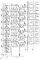
本参考の形態における表示装置のドライバ回路は、液晶表示装置のデータ信号線ドライバである。図1にこのようなデータ信号線ドライバ31の構成を示す。
【0078】
データ信号線ドライバ31は、シフトレジスタ31aとサンプリング部31bとを備えている。
【0079】
シフトレジスタ31aは、複数段のセット・リセット型のフリップフロップSRFF1・SRFF2・…と、複数のスイッチ回路(制御信号供給回路)ASW1・ASW2・…とを備えている。スイッチ回路ASWk(k=1,2,…)はフリップフロップSRFFkのQ出力を導通および非導通の制御信号としている。kが奇数であるスイッチ回路ASWkは、導通すると、後述するタイミングパルスとは別の外部の供給源から供給されるクロック信号(予備充電制御信号(予備充電を行わせるための信号))SCKを取り込んで出力する。また、kが偶数であるスイッチ回路ASWkは、導通すると、同じくタイミングパルスとは別の外部の供給源から供給されるクロック信号(予備充電制御信号)SCKBを取り込んで出力する。クロック信号SCKBはクロック信号SCKの反転信号である。
【0080】
スイッチ回路ASW1・ASW2・…は、フリップフロップSRFFkのQ出力をスイッチV−ASWn(後述)へ送る信号線(第1信号線)S1と分離した信号線(第2信号線)S2を通して、クロック信号SCK・SCKB(後述する出力信号SR1・SR2・…)をスイッチP−ASWn(後述)に出力する。また、スイッチ回路ASW1・ASW2・…は、フリップフロップSRFFkのQ出力をスイッチV−ASWn(後述)へ送る信号線(第1信号線)と分離した信号線を通して、外部の供給源からクロック信号SCK・SCKBを取り込む。
【0081】
スイッチ回路ASW1の出力は出力信号DSR1であり、スイッチ回路ASW2・ASW3・…の出力は順に、出力信号SR1・SR2・…である。各スイッチ回路ASWkの出力信号は、フリップフロップSRFF(k+1)のセット信号となり、また、後述するサンプリング部31bの予備充電回路が備えるスイッチP−ASW(k+1)への入力信号となる。
【0082】
スイッチ回路ASW1・ASW2・…として使用可能なスイッチ回路の一例を図19に基づいて説明する。図19は、スイッチ回路の一例の構成を示す回路図である。
【0083】
スイッチ回路は、上記インバータ回路INV11と、pchトランジスタp11およびnchトランジスタn11によって構成されるCMOSスイッチと、nchトランジスタn12とによって構成されている。外部から入力される制御信号ENに応じて、制御信号ENがHighの場合には、nchトランジスタn12が閉じ、CMOSスイッチのpchトランジスタp11およびnchトランジスタn11は開き、外部から入力された信号CKINが出力信号OUTとしてそのまま出力される。また、制御信号ENがLowになると、CMOSスイッチのpchトランジスタp11およびnchトランジスタn11は閉じ、nchトランジスタn12が開き、出力信号OUTはLowに固定される。制御信号ENは、図1におけるフリップフロップSRFFkのQ出力に相当する。また、入力信号CKINは、図1におけるクロック信号SCKまたはSCKBに相当する。また、出力信号OUTは、図1における出力信号DSR1・SR1・SR2・…に相当する。
【0084】
フリップフロップSRFFkのQ出力は、k=1では出力信号DQ1であり、k=2,3,…に対しては順に出力信号Q1・Q2・…である。スイッチ回路ASW(k+2)の出力信号は、フリップフロップSRFFkのリセット信号となる。初段のフリップフロップSRFF1のセット信号としては、外部から入力されるスタートパルスSSPが入力される。このスタートパルスSSPは、スイッチP−ASWへの入力信号にもなる。フリップフロップSRFF1の出力信号DQ1はスイッチ回路ASW1へ入力され、フリップフロップSRFF2・SRFF3・…の出力信号Q1・Q2・…は順に、後述するサンプリング部31bが備えるバッファBuf1・Buf2・…を介してサンプリング部31bが備えるスイッチV−ASW1・V−ASW2・…に入力される。出力信号Q1・Q2・…は、後述するビデオ信号VIDEOのサンプリングのタイミングパルスとなる。
【0085】
次に、サンプリング部(書き込み回路、予備充電回路)31bは、バッファBuf1・Buf2・…と、スイッチV−ASW1・V−ASW2・…と、予備充電回路とを備えている。予備充電回路は、スイッチP−ASW1・P−ASW2・…を備えている。バッファBuf1・Buf2・…と、スイッチV−ASW1・V−ASW2・…とにより、書き込み回路が構成されている。
【0086】
バッファBufn(n=1,2,…)は、それぞれ4つのインバータが縦続接続されたバッファであり、その入力は前述したようにシフトレジスタ31aから出力される出力信号Qnである。スイッチ(第1スイッチ)V−ASWnは、バッファBufnの出力信号を入力信号とし、その入力信号がゲート(第1制御端子)Gに直接入力されるNチャネルMOSトランジスタ(TFT)およびその入力信号が反転された信号がゲートGに入力されるPチャネルMOSトランジスタ(TFT)からなるアナログスイッチと、上記入力信号を反転してPチャネルMOSトランジスタのゲートに入力するインバータとからなる。各MOSトランジスタのゲートGは容量性の制御端子であり、スイッチV−ASWnは、ゲートの充電電圧に応じて導通と非導通とが切り換わる。各スイッチV−ASWnのアナログスイッチのチャネル経路の一端には外部から供給されるアナログのビデオ信号(書き込み信号)VIDEOが共通に入力される。
【0087】
スイッチ(第2スイッチ)P−ASWnは、前述の説明からも分かるようにフリップフロップSRFFk(k=n)のセット信号を入力信号とし、その入力信号がゲート(第2制御端子)G’に直接入力されるNチャネルMOSトランジスタおよびその入力信号が反転された信号がゲートG’に入力されるPチャネルMOSトランジスタからなるアナログスイッチと、上記入力信号を反転してPチャネルMOSトランジスタのゲートG’に入力するインバータとからなる。各MOSトランジスタのゲートG’は容量性の制御端子であり、スイッチP−ASWnは、ゲートの充電電圧に応じて導通と非導通とが切り換わる。各スイッチP−ASWnのアナログスイッチのチャネル経路の一端には、外部から印加される予備充電電位PVIDが共通に入力される。
【0088】
また、各スイッチV−ASWnのアナログスイッチのチャネル経路の他端と、各スイッチP−ASWnのアナログスイッチのチャネル経路の他端とは、液晶表示パネルに設けられたデータ信号線(信号供給線)SLn(n=1,2,…)に接続されている。液晶表示パネルにはさらに、データ信号線SLnと直交するように走査信号線GL1・GL2・…が設けられている。データ信号線SLnと走査信号線GLm(m=1,2,…)との交点にはマトリクス状に画素Pixm−n(m=1,2,…、n=1,2,…)が形成されている。各画素は、通常のアクティブマトリクス型の液晶表示装置と同じように、NチャネルMOSトランジスタ(TFT)、液晶容量、および補助容量を備えている。走査信号線GLmは所定周期で選択され、選択されている間、走査信号線GLmにつながれている画素のMOSトランジスタを導通させる。
【0089】
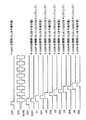
次に、上記の構成のデータ信号線ドライバの動作を、図2に示すタイミングチャートを用いて説明する。
【0090】
ある走査信号線GLmが選択されている1期間について述べる。走査信号線GLmが選択されているので、データ信号線LSへの予備充電では、データ信号線LSとそれに接続されて選択されている画素との両方を充電する。スタートパルスSSPが入力されると、フリップフロップSRFF1から出力信号DQ1が出力されるとともに、スタートパルスSSPはスイッチP−ASW1に入力される。これによりスイッチP−ASW1のアナログスイッチは導通し(以下、スイッチが導通するあるいは非導通になると表現する)、予備充電電位PVIDがデータ信号線SL1に印加される。これにより、データ信号線SL1と、選択されている画素の容量とが予備充電される。このとき、スイッチV−ASW1は非導通であるので、予備充電電位PVIDとビデオ信号VIDEOとがデータ信号線SL1上で衝突することはない。
【0091】
また、出力信号DQ1によってスイッチ回路ASW1が導通し、クロック信号SCKを取り込んで出力信号DSR1を出力する。出力信号DSR1はフリップフロップSRFF2のセット信号となり、フリップフロップSRFF2は出力信号Q1を出力する。出力信号Q1によってスイッチASW2が導通し、スイッチASW2はクロック信号SCKBを取り込んで出力信号SR1を出力する。また、出力信号Q1はタイミングパルスとしてバッファBuf1を介してスイッチV−ASW1を導通させる。これにより、データ信号線SL1にはビデオ信号VIDEOが供給され、データ信号線SL1および画素容量が所定の電圧に充電される。すなわち、ビデオ信号VIDEOのサンプリングが行われ、上記所定周期中の各データ信号線が順次サンプリングの期間となるサンプリング実効期間(書き込み実効期間)が開始される。
【0092】
このときすでにスタートパルスSSPはLowになっているため、スイッチP−ASW1は非導通となっており、予備充電電位PVIDとビデオ信号VIDEOとがデータ信号線SL1上で衝突することはない。また、出力信号DSRによってスイッチP−ASW2が導通するので、ビデオ信号VIDEOがデータ信号線SL1に出力されると同時に、データ信号線SL2および画素容量が予備充電される。一方、出力信号SR1はフリップフロップSRFF1のリセット信号となるので、SRFF1の出力信号DQ1はLowになる。これにより、スイッチASW1は非導通になる。
【0093】
このようにして、データ信号線SLnの予備充電を行った後にデータ信号線SLnにビデオ信号VIDEOを供給し、このビデオ信号VIDEOの供給の間にデータ信号線SL(n+1)の予備充電を行うという動作を順次繰り返し、点順次でサンプリングが行われていく。この動作は、フリップフロップSRFFkとスイッチASWkとによって、タイミングパルスがシフトレジスタ中を後段のフリップフロップSRFFへ向けて順次転送されていく動作に準じている。図2に示すように、前後する各サンプリングの期間はクロック信号SCK・SCKBの半周期分ずつ重複している。この場合、各サンプリングの期間におけるタイミングパルスの立ち下がり時の画素容量およびデータ信号線の充電電位でサンプリング電位が決定される。
【0094】
先に述べたサンプリング実効期間は、最終段のデータ信号線ドライバSLにおけるサンプリングが終了するまでの期間であり、この期間の間に行うサンプリングの期間中でないデータ信号線への予備充電は、タイミングパルスとは別の供給源から入力されるクロック信号SCK・SCKBがスイッチ回路ASWkによって取り込まれて出力され、制御端子(ゲートG’)が充電されてスイッチP−ASWn(n=k+1)が導通することにより行われる。サンプリング実効期間に常にこのような予備充電を行うようにするため、スイッチ回路ASWkの総数は、サンプリング実効期間に予備充電を行うデータ信号線SLの数に等しくなっている。サンプリング実効期間外に行う予備充電(例えばデータ信号線LS1への予備充電)については、必ずしもこのようなスイッチ回路を用いなくてよい。
【0095】
このように、データ信号線SLにビデオ信号VIDEOのサンプリングを行っている間に、別のデータ信号線SLの予備充電を行うことができる。また、このときに、サンプリングのタイミングパルスが供給される系統と、予備充電を行わせる信号が供給される系統とは分離されるので、スイッチV−ASWの制御信号回路とP−ASWの制御信号回路とが共用されることはない。これにより、予備充電に伴ってデータ信号線SLに流れる大きな電流が、スイッチP−ASWの容量性の制御端子(ゲートG’)を介して、そのときに書き込みを行っているデータ信号線SLのビデオ信号VIDEOの電位を揺動させてしまうことを回避することができる。また、クロック信号SCK・SCKBを取り込んで出力する各スイッチ回路ASWkはフリップフロップよりも簡単に構成することができるので、シフトレジスタ31aの回路規模は、従来のようにシフトレジスタを2倍にする場合よりもはるかに抑制される。
【0096】
以上により、予備充電回路を内部に備え、信号供給線に駆動能力の小さい予備充電電源から予備充電を行う場合に、シフトレジスタの回路規模を抑制しながら、他の信号供給線に供給される信号の揺動を回避することのできる表示装置のドライバ回路を提供することができる。
【0097】
なお、特許文献4に対して、本参考の形態では、データ信号線の予備充電を行うための制御信号としてクロック信号を取り込み、予備充電電位をデータ信号線へ印加するためのスイッチへ入力するという全く新しい思想を導入している。
【0098】
〔参考の形態2〕
本発明の他の参考の形態について、図3および図4を用いて説明すれば、以下の通りである。なお、前記参考の形態1で述べた構成要素と同一の機能を有する構成要素には同一の符号を付し、その説明を省略する。
【0099】
本参考の形態における表示装置のドライバ回路は、液晶表示装置のデータ信号線ドライバである。図3にこのようなデータ信号線ドライバ32の構成を示す。
【0100】
データ信号線ドライバ32は、シフトレジスタ32aとサンプリング部(書き込み回路、予備充電回路)32bとを備えている。
【0101】
シフトレジスタ32aは図1のシフトレジスタ31aと内部構成は同じであるが、予備充電用の信号の出力先が異なっている。フリップフロップSRFF1のセット信号となるスタートパルスSSPは、予備充電用の信号としては、スイッチP−ASW2に入力される。また、出力信号DSR1はスイッチP−ASW3に入力される。さらに、出力信号SR(k−1)(k=2,3,…)はスイッチP−ASWn(n=k+2)に入力される。
【0102】
サンプリング部32bは、図1のサンプリング部31bからスイッチP−ASW1を取り除いた構成である。また、図1のデータ信号線SL1はダミーのデータ信号線DSLに置き換えられ、図1のデータ信号線SL2・SL3・…が順に図3ではデータ信号線SL1・SL2・…に置き換えられている。また、データ信号線DSLに接続される画素はダミーの画素Pixm−D(m=1,2,…)に置き換えられ、データ信号線SL1・SL2・…に接続される画素はその分、水平方向にシフトされている。すなわち、本参考の形態のデータ信号線ドライバ32は、ダミーのデータ信号線および画素を備えた表示装置のドライバ回路として好適に用いられる。
【0103】
図4は、上記構成のデータ信号線ドライバ32の動作を示すタイミングチャートである。信号伝達の原理は図1の場合と同じであるので詳細な説明は省略する。特徴的なことは、例えば、スタートパルスSSPによってスイッチP−ASW2が導通することにより、データ信号線SL1が予備充電された後、クロック信号SCK・SCKBの半周期だけ時間が経過してからデータ信号線SL1へのサンプリングが行われるといったように、同じデータ信号線SLへの予備充電の終了時とサンプリングの開始時とがクロック信号SCK・SCKBの半周期分だけずれていることである。
【0104】
これにより、参考の形態1で述べた効果に加えて、予備充電電位PVIDとビデオ信号VIDEOとの衝突を確実に回避することができ、それだけ高品位の表示を得ることができるという効果がある。なお、上述したダミーの画素は、通常、ブラックマトリクスと呼ばれる遮光体の下に設けられるため、その画素の表示は画面には現れない。従って、ダミーの画素およびデータ信号線への予備充電を行う必要はない。
【0105】
〔参考の形態3〕
本発明のさらに他の参考の形態について、図5および図6を用いて説明すれば、以下の通りである。なお、前記参考の形態1および2で述べた構成要素と同一の機能を有する構成要素には同一の符号を付し、その説明を省略する。
【0106】
本参考の形態における表示装置のドライバ回路は、液晶表示装置のデータ信号線ドライバである。図5にこのようなデータ信号線ドライバ33の構成を示す。
【0107】
データ信号線ドライバ33は、シフトレジスタ33aとサンプリング部(書き込み回路、予備充電回路)33bとを備えている。
【0108】
シフトレジスタ33aは、複数段のDフリップフロップであるフリップフロップDFFD1・DFF1・DFF2・…と、複数のスイッチ回路ASWD1・ASW1・ASW2・…とを備えている。初段のフリップフロップDFFD1の入力信号INはスタートパルスSSPであり、各フリップフロップのQ出力は次段のフリップフロップの入力信号INとなるように、各フリップフロップが縦続接続されている。また、上記スイッチ回路のそれぞれは互いに同じ構成であり、スイッチ回路ASWD1はスタートパルスSSPを、スイッチ回路ASW1はフリップフロップDFFD1のQ出力を、スイッチ回路ASW2・ASW3・…は順にフリップフロップDFF1・DFF2・…のQ出力を、それぞれ導通および非導通の制御信号としている。
【0109】
スイッチ回路ASWD1とkが偶数であるスイッチ回路ASWkとは、導通すると、後述するタイミングパルスとは別の外部の供給源から供給される各フリップフロップの動作用のクロック信号SCKを取り込んで出力する。また、kが奇数であるスイッチ回路ASWkは、導通すると、同じくタイミングパルスとは別の外部の供給源から供給される各フリップフロップの動作用のクロック信号SCKBを取り込んで出力する。クロック信号SCK・SCKBは、各フリップフロップにおいては内部のクロックト・インバータの動作用に用いられる。
【0110】
スイッチ回路ASWD1の出力は出力信号DSR1であり、スイッチ回路ASW1の出力は出力信号DSR2であり、スイッチ回路ASW2・ASW3・…の出力は順に、出力信号SR1・SR2・…である。各スイッチ回路ASWD1・ASW1・ASW2・…の出力信号は順に、後述するサンプリング部33bの予備充電回路が備えるスイッチP−ASW1・P−ASW2・P−ASW3・…への入力信号となる。
【0111】
フリップフロップDFFD1のQ出力は出力信号DQ1であり、フリップフロップDFFn(n=1,2,…)のQ出力は出力信号Qnである。フリップフロップDFFnの出力信号Qnは、後述するサンプリング部33bが備えるバッファBufnを介してサンプリング部33bが備えるスイッチV−ASWnに入力される。出力信号Qnは、後述するビデオ信号VIDEOのサンプリングのタイミングパルスとなる。
【0112】
また、サンプリング部(書き込み回路)33bの内部構成は図1のサンプリング部31bと同じであり、シフトレジスタ33aとの接続関係が上述したようになっている。また、データ信号線SLn(n=1,2,…)、走査信号線SLm(m=1,2,…)、および画素Pixm−n(m=1,2,…、n=1,2,…)は図1と同じである。
【0113】
ここで、レベルシフト回路LSD0・LSD1・LS1・LS2・…として使用可能なレベルシフト回路の一例について、図16に基づいて以下に説明する。図16は、レベルシフト回路の一例の構成を示す回路図である。
【0114】
レベルシフト回路は、外部から入力される制御信号ENがHighになると、外部からクロック信号SCK・SCKBを取り込み、クロック信号SCKをレベルシフトした信号を出力信号OUTとして出力するものである。制御信号ENは、図7におけるフリップフロップのQ出力に相当する。また、出力信号OUTは、図7における出力信号DLS1・LR1・LR2・…に相当する。
【0115】
ただし、レベルシフト回路がレベルシフト回路LSD0である場合には、クロック信号SCK・SCKBに代えてスタートパルスSSP・SSPBを取り込み、クロック信号SSPをレベルシフトした信号を出力信号OUTとして出力する。
【0116】
図16のレベルシフト回路は、外部からの制御信号ENに応じて動作を制御され、制御信号ENがHighの場合に動作を開始する。また、本レベルシフト回路は、制御信号ENがLowの場合には常に、出力信号OUTとしてLowを出力するようになっている。
【0117】
図16の記号及び図17のタイミングチャートを用いて、上記レベルシフト回路の動作を以下に説明する。図17は、上記レベルシフト回路における入力信号、ノードの信号、および出力信号の波形を示すタイミングチャートである。
【0118】
今、図17のタイミングチャートが示すように制御信号ENがHighであり、クロック信号CKがHighになると、制御信号ENに応じて、pchトランジスタp3・p4が閉じ、nchトランジスタn1・n2が開く。このとき、pchトランジスタp1・p2およびnchトランジスタn3・n4により、ノードaには、クロック信号CKがHighのときには、pchトランジスタp2を介してHighの信号が入力され、ノードaはHighとなる。次に、クロック信号CKがLowとなると、ノードaにはnchトランジスタn4を介してLowの信号が入力され、ノードaはLowとなる。ノードaのそれぞれの状態(HighまたはLow)は、インバータ回路INV1・INV2によってレベルシフト回路の出力端に伝達され、出力信号OUTとして出力される。この信号は、レベルシフトされたクロック信号CKとなって出力端に現れる。
【0119】
次に、制御信号ENがLowとなると、pchトランジスタp3・p4が開く一方、nchトランジスタn1・n2が閉じる。このとき、pchトランジスタp1・p2のゲートには、電源VCCから電源電圧VCCが、pchトランジスタp3・p4を介して入力される。これにより、pchトランジスタp1・p2は閉じ、電源VCCから流れる電流のパスがなくなる。また、nchトランジスタn3のゲートには、pchトランジスタp1・p2のゲートと同様に、電源電圧VCCが与えられるので、nchトランジスタn3が開き、ノードaはLowとなる。これによって、上記レベルシフト回路の出力信号OUTはLowとなる。したがって、クロック信号CKが電源電圧VCCより低い電位の振幅で入力されても、上記レベルシフト回路の出力信号OUTはLowとして得られる。また、制御信号ENがLowの場合には、電源VCCよりの電流の流れるパスがなくなるため、必要外の電力消費を抑えることが可能となる。
【0120】
また、動作の説明はしないが、図18の構成を備えるレベルシフト回路であっても図16のレベルシフト回路と同様の効果が得られる。なお、図18は、レベルシフト回路の他の一例の構成を示す回路図である。
【0121】
次に、上記構成のデータ信号線ドライバ33の動作について、図6のタイミングチャートを用いて説明する。
【0122】
ある走査信号線GLmが選択されている1期間について述べる。走査信号線GLmが選択されているので、データ信号線LSへの予備充電では、データ信号線LSとそれに接続されて選択されている画素との両方を充電する。スタートパルスSSPが入力されると、スイッチ回路ASWD1は導通し、クロック信号SCKを取り込んで出力信号DSR1を出力する。これにより、スイッチP−ASW1が導通してデータ信号線SL1に予備充電電位PVIDが印加され、データ信号線SL1と画素容量とに予備充電が行われる。また、フリップフロップDFFD1はクロック信号SCKの立ち上がり時にスタートパルスSSPを出力信号DQ1として出力し始め、クロック信号SCKの次の立ち上がり時までこれを保持する。フリップフロップDFF1は、出力信号DQ1が入力されている間、クロック信号SCKBの立ち上がり時に出力信号DQ1を出力信号Q1として出力し始め、クロック信号SCKBの次の立ち上がり時までこれを保持する。出力信号Q1がHighの間は出力信号Q1はサンプリングのタイミングパルスとしてバッファBuf1を介してスイッチV−ASW1を導通させる。これにより、データ信号線SL1および画素容量にビデオ信号VIDEOのサンプリングが行われる。これにより、サンプリング実効期間(書き込み実効期間)が開始される。このとき、すでに出力信号DSR1はLowになっているため、スイッチP−ASW1は非導通になっており、予備充電電位PVIDとビデオ信号VIDEOとがデータ信号線SL1上で衝突することはない。
【0123】
また、出力信号DQ1によりスイッチ回路ASW1は導通し、クロック信号SCKBを取り込んで出力信号DSR2を出力するので、データ信号線SL1にサンプリングが行われている間には、データ信号線SL2の予備充電が行われる。
【0124】
このようにして、データ信号線SLnの予備充電を行った後にデータ信号線SLnにビデオ信号VIDEOを供給し、このビデオ信号VIDEOの供給の間にデータ信号線SL(n+1)の予備充電を行うという動作を順次繰り返し、点順次でサンプリングが行われていく。この動作は、フリップフロップDFFD1・DFF1・DFF2・…によって、タイミングパルスがシフトレジスタ中を後段のフリップフロップへ向けて順次転送されていく動作に準じている。図6に示すように、前後する各サンプリングの期間はクロック信号SCK・SCKBの半周期分ずつ重複している。この場合、各サンプリングの期間におけるタイミングパルスの立ち下がり時の画素容量およびデータ信号線の充電電位でサンプリング電位が決定される。
【0125】
先に述べたサンプリング実効期間は、最終段のデータ信号線ドライバSLにおけるサンプリングが終了するまでの期間であり、この期間の間に行うサンプリングの期間中でないデータ信号線SLへの予備充電は、タイミングパルスとは別の供給源から入力されるクロック信号SCK・SCKBがスイッチ回路ASWD1・ASW1・ASW2・…によって取り込まれて出力され、制御端子(ゲートG’)が充電されてスイッチP−ASWnが導通することにより行われる。サンプリング実効期間に常にこのような予備充電を行うようにするため、スイッチ回路ASWkの総数は、サンプリング実効期間に予備充電を行うデータ信号線SLの数に等しくなっている。サンプリング実効期間外に行う予備充電(例えばデータ信号線SL1への予備充電)については、必ずしもこのようなスイッチ回路を用いなくてよい。
【0126】
このように、データ信号線SLにビデオ信号VIDEOのサンプリングを行っている間に、別のデータ信号線SLの予備充電を行うことができる。また、このときに、サンプリングのタイミングパルスが供給される系統と、予備充電を行わせる信号が供給される系統とは分離されるので、スイッチV−ASWの制御信号回路とP−ASWの制御信号回路とが共用されることはない。これにより、予備充電に伴ってデータ信号線SLに流れる大きな電流が、スイッチP−ASWの容量性の制御端子(ゲートG’)を介して、そのときに書き込みを行っているデータ信号線SLのビデオ信号VIDEOの電位を揺動させてしまうことを回避することができる。また、クロック信号SCK・SCKBを取り込んで出力する各スイッチ回路ASWD1・ASWkはフリップフロップよりも簡単に構成することができるので、シフトレジスタ33aの回路規模は、従来のようにシフトレジスタを2倍にする場合よりもはるかに抑制される。
【0127】
以上により、予備充電回路を内部に備え、信号供給線に駆動能力の小さい予備充電電源から予備充電を行う場合に、シフトレジスタの回路規模を抑制しながら、他の信号供給線に供給される信号の揺動を回避することのできる表示装置のドライバ回路を提供することができる。
【0128】
〔実施の形態1〕
本発明の一実施の形態について、図7および図8を用いて説明すれば、以下の通りである。なお、前記参考の形態1ないし3で述べた構成要素と同一の機能を有する構成要素には同一の符号を付し、その説明を省略する。
【0129】
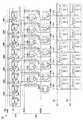
本実施の形態における表示装置のドライバ回路は、液晶表示装置のデータ信号線ドライバである。図7にこのようなデータ信号線ドライバ34の構成を示す。
【0130】
データ信号線ドライバ34は、シフトレジスタ34aとサンプリング部(書き込み回路、予備充電回路)34bとを備えている。
【0131】
シフトレジスタ34aは、図1のフリップフロップSRFFk(k=1,2,…)と、レベルシフト回路LSD0・LSD1・LS1・LS2・…とを備えている。レベルシフト回路LSD1・LS1・LS2・…は順に、図1のスイッチ回路ASW1・ASW2・ASW3・…を置き換えたものとなっている。レベルシフト回路LSD1・LS1・LS2・…のそれぞれは互いに同じ構成であり、フリップフロップのHighのQ出力が入力されるとクロック信号SCK・SCKBを取り込み、これらを用いてレベルシフトを行う。レベルシフト回路LSD1・LS2・LS4・…はクロック信号SCKの波形のレベルシフトを行い、レベルシフト回路LSD1・LS1・LS3・…はクロック信号SCKBの波形のレベルシフトを行う。そして、レベルシフト回路LSD1・LS1・LS2・…のそれぞれは、レベルシフトの結果として、順に出力信号DLS1・LR1・LR2・…(予備充電制御信号)を出力する。これらの出力信号はそれぞれ次段のフリップフロップのセット信号となる。
【0132】
また、レベルシフト回路LSD0は、初段のフリップフロップに入力されるスタートパルスSSPのレベルシフトを行うために、スタートパルスSSP・SSPBが入力されるレベルシフト回路である。スタートパルスSSPBはスタートパルスSSPの反転信号である。レベルシフト回路LSD0は、スタートパルスSSPのレベルシフトを行って出力信号DLR0として出力する。
【0133】
すなわち、本実施の形態のデータ信号線ドライバ34は、外部から入力されるクロック信号SCK・SCKBやスタートパルス信号SSPといった信号の電圧レベルが低い場合の表示装置のドライバ回路として好適に用いられるものである。
【0134】
サンプリング部34bは図1のサンプリング部31bと内部構成は同じである。シフトレジスタ34aの出力信号DLS0・DLS1・LR1・LR2・…は順に、スイッチP−ASW1・P−ASW2・P−ASW3・P−ASW4・…の入力信号となる。
【0135】
また、データ信号線SLn(n=1,2,…)、走査信号線SLm(m=1,2,…)、および画素Pixm−n(m=1,2,…、n=1,2,…)は図1と同じである。
【0136】
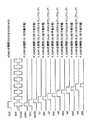
次に、上記の構成のデータ信号線ドライバ34の動作を、図8に示すタイミングチャートを用いて説明する。
【0137】
ある走査信号線GLmが選択されている1期間について述べる。走査信号線GLmが選択されているので、データ信号線LSへの予備充電では、データ信号線LSとそれに接続されて選択されている画素との両方を充電する。スタートパルスSSP・SSPBが入力されると、レベルシフト回路LSD0がこれのレベルシフトを行って出力信号DLR0を出力する。すると、フリップフロップSRFF1から出力信号DQ1が出力されるとともに、スタートパルスSSPはスイッチP−ASW1に入力される。これによりスイッチP−ASW1は導通し、予備充電電位PVIDがデータ信号線SL1に印加される。これにより、データ信号線SL1と、選択されている画素の容量とが予備充電される。このとき、スイッチV−ASW1は非導通であるので、予備充電電位PVIDとビデオ信号VIDEOとがデータ信号線SL1上で衝突することはない。
【0138】
また、出力信号DQ1が入力されることによってレベルシフト回路LSD1はクロック信号SCK・SCKBを取り込んでクロック信号SCKのレベルシフトを行い出力信号DLS1を出力する。出力信号DLS1はフリップフロップSRFF2のセット信号となり、フリップフロップSRFF2は出力信号Q1を出力する。出力信号Q1が入力されることによってレベルシフト回路LS1はクロック信号SCKB・SCKを取り込んでクロック信号SCKBのレベルシフトを行い出力信号LR1を出力する。また、出力信号Q1はタイミングパルスとしてバッファBuf1を介してスイッチV−ASW1を導通させる。これにより、データ信号線SL1にはビデオ信号VIDEOが供給され、データ信号線SL1および画素容量が所定の電圧に充電される。すなわち、ビデオ信号VIDEOのサンプリングが行われ、上記所定周期中の各データ信号線が順次サンプリングの期間となるサンプリング実効期間(書き込み実効期間)が開始される。
【0139】
このときすでにスタートパルスSSPおよび出力信号DLR0はLowになっているため、スイッチP−ASW1は非導通となっており、予備充電電位PVIDとビデオ信号VIDEOとがデータ信号線SL1上で衝突することはない。また、出力信号DLS1によってスイッチP−ASW2が導通するので、ビデオ信号VIDEOがデータ信号線SL1に出力されると同時に、データ信号線SL2および画素容量が予備充電される。一方、出力信号LR1はフリップフロップSRFF1のリセット信号となるので、SRFF1の出力信号DQ1はLowになる。これにより、レベルシフト回路LSD1はレベルシフト動作を停止する。
【0140】
なお、シフトレジスタを構成するフリップフロップとして互いに縦続接続されるDフリップフロップを用いたとすれば、上記のようにレベルシフト回路の動作の実行および停止を制御するためには、各段のDフリップフロップの入力信号と出力信号との両方を用いなければならない。これに対して本実施の形態におけるシフトレジスタ34aにはセット・リセットフリップフロップを用いているので、レベルシフト回路の動作の実行および停止を制御するためには、前段のフリップフロップの出力信号のみを用いればよいので、構成が簡略化される。
【0141】
このようにして、データ信号線SLnの予備充電を行った後にデータ信号線SLnにビデオ信号VIDEOを供給し、このビデオ信号VIDEOの供給の間にデータ信号線SL(n+1)の予備充電を行うという動作を順次繰り返し、点順次でサンプリングが行われていく。この動作は、フリップフロップSRFFkと各レベルシフト回路とによって、タイミングパルスがシフトレジスタ中を後段へ向けて順次転送されていく動作に準じている。図8に示すように、前後する各サンプリングの期間はクロック信号SCK・SCKBの半周期分ずつ重複している。この場合、各サンプリングの期間におけるタイミングパルスの立ち下がり時の画素容量およびデータ信号線SLの充電電位でサンプリング電位が決定される。
【0142】
先に述べたサンプリング実効期間は、最終段のデータ信号線ドライバSLにおけるサンプリングが終了するまでの期間であり、この期間の間に行うサンプリングの期間中でないデータ信号線SLへの予備充電は、タイミングパルスとは別の供給源から入力されるクロック信号SCK・SCKBがレベルシフト回路LSD1・LS1・LS2・…によって取り込まれて出力され、制御端子(ゲートG’)が充電されてスイッチP−ASWnが導通することにより行われる。サンプリング実効期間に常にこのような予備充電を行うようにするため、レベルシフト回路LSD1・LS1・LS2・…の総数は、サンプリング実効期間に予備充電を行うデータ信号線SLの数に等しくなっている。サンプリング実効期間外に行う予備充電(例えばデータ信号線SL1への予備充電)については、必ずしもこのようなレベルシフト回路を用いなくてよい。
【0143】
このように、データ信号線SLにビデオ信号VIDEOのサンプリングを行っている間に、別のデータ信号線SLの予備充電を行うことができる。また、このときに、サンプリングのタイミングパルスが供給される系統と、予備充電を行わせる信号が供給される系統とは分離されるので、スイッチV−ASWの制御信号回路とP−ASWの制御信号回路とが共用されることはない。これにより、予備充電に伴ってデータ信号線SLに流れる大きな電流が、スイッチP−ASWの容量性の制御端子(ゲートG’)を介して、そのときに書き込みを行っているデータ信号線SLのビデオ信号VIDEOの電位を揺動させてしまうことを回避することができる。また、クロック信号SCK・SCKBを取り込んでレベルシフトを行って出力する各レベルシフト回路LSD1・LS1・LS2・…、およびレベルシフト回路LSD0はフリップフロップよりも簡単に構成することができるので、シフトレジスタ34aの回路規模は、従来のようにシフトレジスタを2倍にする場合よりもはるかに抑制される。
【0144】
以上により、予備充電回路を内部に備え、信号供給線に駆動能力の小さい予備充電電源から予備充電を行う場合に、シフトレジスタの回路規模を抑制しながら、他の信号供給線に供給される信号の揺動を回避することのできる表示装置のドライバ回路を提供することができる。
【0145】
また、レベルシフト回路に入力されるクロック信号は低電圧信号でよいことから分かるように、レベルシフト回路は低電圧インタフェースとしての機能を備えており、クロック信号を発生する外部回路の低消費電力化を図ることができる。
【0146】
なお、特許文献5および特許文献6に対して、本実施の形態では、データ信号線の予備充電を行うための制御信号を、クロック信号のレベルシフトを行って生成し、予備充電電位をデータ信号線へ印加するためのスイッチへ入力するようにするという全く新しい思想を導入している。
【0147】
〔実施の形態2〕
本発明のさらに他の実施の形態について、図9および図10を用いて説明すれば、以下の通りである。なお、前記参考の形態1ないし3および実施の形態1で述べた構成要素と同一の機能を有する構成要素には同一の符号を付し、その説明を省略する。
【0148】
データ信号線ドライバ35は、シフトレジスタ35aとサンプリング部(書き込み回路、予備充電回路)35bとを備えている。
【0149】
シフトレジスタ35aは図7のシフトレジスタ34aと内部構成は同じであるが、予備充電用の信号の出力先が異なっている。フリップフロップSRFF1のセット信号となる出力信号DLR0は、予備充電用の信号としては、スイッチP−ASW2に入力される。また、出力信号DLS1はスイッチP−ASW3に入力される。さらに、出力信号LR1・LR2・…はスイッチP−ASW4・P−ASW5・…に入力される。
【0150】
サンプリング部35bは、図7のサンプリング部34bからスイッチP−ASW1を取り除いた構成である。また、図7のデータ信号線SL1はダミーのデータ信号線DSLに置き換えられ、図7のデータ信号線SL2・SL3・…が順に図9ではデータ信号線SL1・SL2・…に置き換えられている。また、データ信号線DSLに接続される画素はダミーの画素Pixm−D(m=1,2,…)に置き換えられ、データ信号線SL1・SL2・…に接続される画素はその分、水平方向にシフトされている。すなわち、本実施の形態のデータ信号線ドライバ35は、ダミーのデータ信号線および画素を備えた表示装置のドライバ回路として好適に用いられる。
【0151】
図10は、上記構成のデータ信号線ドライバ35の動作を示すタイミングチャートである。信号伝達の原理は図7の場合と同じであるので詳細な説明は省略する。特徴的なことは、例えば、スタートパルスSSP、従って出力信号DLR0によってスイッチP−ASW2が導通することにより、データ信号線SL1が予備充電された後、クロック信号SCK・SCKBの半周期だけ時間が経過してからデータ信号線SL1へのサンプリングが行われるといったように、同じデータ信号線SLへの予備充電の終了時とサンプリングの開始時とがクロック信号SCK・SCKBの半周期だけずれていることである。
【0152】
これにより、実施の形態1で述べた効果に加えて、予備充電電位PVIDとビデオ信号VIDEOとの衝突を確実に回避することができ、それだけ高品位の表示を得ることができるという効果がある。なお、上述したダミーの画素は、通常、ブラックマトリクスと呼ばれる遮光体の下に設けられるため、その画素の表示は画面には現れない。従って、ダミーの画素およびデータ信号線への予備充電を行う必要はない。
【0153】
〔実施の形態3〕
本発明のさらに他の実施の形態について、図11を用いて説明すれば、以下の通りである。なお、前記参考の形態1ないし3および実施の形態1,2で述べた構成要素と同一の機能を有する構成要素には同一の符号を付し、その説明を省略する。
【0154】
図11に本実施の形態の表示装置である液晶表示装置1の構成を示す。
【0155】
液晶表示装置1は画素の点順次かつ交流駆動を行うアクティブマトリクス型の液晶表示装置であり、マトリクス状に配された画素Pixを有する表示部2と、各画素Pixを駆動するデータ信号線ドライバ3および走査信号線ドライバ4と、制御回路5と、データ信号線SL…および走査信号線GL…とを備えている。制御回路5が各画素Pixの表示状態を示すビデオ信号VIDEOを生成すると、このビデオ信号VIDEOに基づいて画像を表示することができる。
【0156】
ここで、表示部2は参考の形態1ないし3および実施の形態1,2で述べた画素Pixm−n(m=1,2,…、n=1,2,…)およびダミーの画素と同じものである。データ信号線ドライバ3には、参考の形態1ないし3および実施の形態1,2で述べたデータ信号線ドライバ31〜35のいずれかを用いている。データ信号線ドライバ3のシフトレジスタ3aおよびサンプリング部(書き込み回路、予備充電回路)3bは、参考の形態1ないし3および実施の形態1,2で述べたシフトレジスタ31a〜35aおよびサンプリング部31b〜35bに相当する。
【0157】
また、走査信号線ドライバ4は、参考の形態1ないし3および実施の形態1,2で述べた走査信号線GLnを線順次に駆動してそれぞれに接続された画素のMOSFET(TFT)を選択する回路である。また、走査信号線ドライバ4は走査信号線GLの選択を線順次で行うタイミング信号を転送するためのシフトレジスタ4aを備えている。
【0158】
上記表示部2、データ信号線ドライバ3、および走査信号線ドライバ4は、製造時の手間と、配線容量とを削減するために、同一基板上に設けられている。また、より多くの画素Pixを集積し、表示面積を拡大するために、上記表示部2、データ信号線ドライバ3、および走査信号線ドライバ4は、ガラス基板上に形成された多結晶シリコン薄膜トランジスタから構成されている。さらに、通常のガラス基板(歪み点が600度以下のガラス基板)を用いても、歪み点以上のプロセスに起因するソリやタワミが発生しないように、上記多結晶薄膜シリコントランジスタは、600度以下のプロセス温度で製造される。
【0159】
また、制御回路5は、クロック信号SCK・SCKB、スタートパルスSSP、予備充電電位PVID、およびビデオ信号VIDEOを生成してデータ信号線ドライバ3へ向けて出力する。さらに制御回路5は、クロック信号GCK、スタートパルスGSP、および信号GPSを生成して走査信号線ドライバ4へ向けて出力する。
【0160】
上記の構成により、液晶表示装置1では参考の形態1ないし3および実施の形態1,2で述べた効果が得られ、高い表示品位で表示を行うことができる。
【0161】
また、本発明の表示装置は液晶表示装置に限らず、有機EL表示装置などでもよく、配線容量を充電する必要のある表示装置であればどのようなものでもよい。
【0162】
〔実施の形態4〕
本発明のさらに他の実施の形態について、図12ないし図15に基づいて説明すれば、以下の通りである。なお、前記参考の形態1ないし3および実施の形態1ないし3で述べた構成要素と同一の機能を有する構成要素には同一の符号を付し、その説明を省略する。
【0163】
前記参考の形態1ないし3および実施の形態1,2の表示装置のドライバ回路は、複数のデータ信号線に順次書き込みを行う、いわゆる点順次駆動方式のドライバ回路示している。例えば、参考の形態1の表示装置のドライバ回路をみると、サンプリング用のスイッチV−ASWの導通・非導通を制御するシフトレジスタの出力Qと、シフトレジスタを構成するフリップフロップSRFFの次段へのセット信号および予備充電用のスイッチP−ASWの導通・非導通を制御する信号SRが、それぞれ1系統のスイッチに関連する事例について説明してきたが、図12に示すようにサンプリングがRGB信号の3系統のものにも本発明は適用可能である。
【0164】
また、図13に示すようにビデオ信号を複数系統に相展開して、ビデオ信号のサンプリング周期を遅くするようなものにも本発明は適用可能である。なお、図面を簡略化して作成しているため、予備充電用のスイッチおよび本サンプリング用のスイッチを図12とは異なる記号で示しているが、実際には図14に示すように同じものを用いていると考えてよい。同様に、本サンプリング用アナログスイッチを駆動するためのバッファ群も図12とは異なる記号で示しているが、図15に示すように同じものを用いていると考えてよい。同様に、シフトレジスタも図12とは異なるものではなく、実際には図12と同じような構成であると考えてよい。但し、バッファ群は、予備充電およびサンプリングの系統数に対して十分な駆動能力のものとする必要がある。
【0165】
ここで、図12および図13のように、信号供給線のi(iは2以上の整数)本を1単位としてサンプリングをi系統にする場合には、フリップフロップからのタイミングパルスにより、サンプリング用のスイッチを単位内で同時にかつ各単位毎で順次に導通させるとともに、スイッチ回路を単位の数に対応して備え、予備充電用のスイッチを単位内で同時にかつ各単位毎で順次に導通させている。基本的な動作は1系統の場合と同様であるが、サンプリング用のスイッチおよび予備充電用のスイッチを複数個同時に導通させていることが異なる点である。
【0166】
さらに、本発明は、図12および図13に限定されることはなく、参考の形態1ないし3および実施の形態1,2の表示装置のドライバ回路において、図12および図13のように予備充電およびサンプリングの系統数を複数にしたものを適用することができる。
【0167】
【発明の効果】
本発明の参考に係る表示装置のドライバ回路は、以上のように、複数の信号供給線が設けられた表示装置のためのドライバ回路であって、容量性の第1制御端子の充電電圧に応じて導通と非導通とが切り換わる第1スイッチを、上記複数の信号供給線のそれぞれに対して備え、各上記信号供給線に対する書き込み信号の書き込みを各上記第1スイッチの導通により行う書き込み回路と、上記書き込みのタイミングパルスを上記第1スイッチの第1制御端子へ向けて出力するフリップフロップを、上記タイミングパルスを順次転送して上記書き込みが所定周期で行われるように複数段備えたシフトレジスタと、容量性の第2制御端子の充電電圧に応じて導通と非導通とが切り換わる第2スイッチを上記信号供給線のそれぞれに対して備え、各上記信号供給線への予備充電を各上記第2スイッチの導通により行う予備充電回路とを備え、上記予備充電回路は、一部の信号供給線に対して上記書き込み回路による書き込み信号の書き込みが行われている間に、他の信号供給線の予備充電を行うものであり、上記シフトレジスタは、上記タイミングパルスを上記第1制御端子へ送る第1信号線とは分離した第2信号線を通して、第2スイッチの導通を制御する予備充電制御信号を上記第2制御端子に出力する制御信号供給回路を備えている構成である。
【0168】
それゆえ、信号供給線に書き込み信号の書き込みを行っている間に、別の信号供給線の予備充電を行うことができる。また、このときに、第1スイッチの制御信号回路と第2スイッチの制御信号回路とが共用されることはない。これにより、予備充電に伴って信号供給線に流れる大きな電流が、第1スイッチの容量性の第1制御端子および第2スイッチの容量性の第2の制御端子を介して、そのときに書き込みを行っている信号供給線の書き込み信号の電位を揺動させてしまうことを回避することができる。また、第2スイッチの導通を制御する予備充電制御信号を上記第2制御端子に出力する制御信号供給回路はフリップフロップよりも簡単に構成することができるので、シフトレジスタの回路規模は、従来のようにシフトレジスタを2倍にする場合よりもはるかに抑制される。
【0169】
以上により、予備充電回路を内部に備え、信号供給線に駆動能力の小さい予備充電電源から予備充電を行う場合に、シフトレジスタの回路規模を抑制しながら、他の信号供給線に供給される信号の揺動を回避することのできる表示装置のドライバ回路を提供することができるという効果を奏する。
【0170】
本発明の参考に係る表示装置のドライバ回路は、以上のように、上記フリップフロップはセット・リセットフリップフロップであり、上記シフトレジスタは、上記所定周期中で各上記信号供給線が上記書き込みの期間となる書き込み実効期間に、転送される上記タイミングパルスが上記セット・リセットフリップフロップから入力されると、上記タイミングパルスとは別の供給源から入力されるクロック信号を取り込んで上記書き込みの期間中でない所定の上記信号供給線に対応する上記第2スイッチの制御端子へ向けて出力して該第2スイッチを導通させるスイッチ回路を、上記書き込み実効期間に上記予備充電を行う上記信号供給線に対応するように複数個備えており、各上記スイッチ回路は、取り込んだ上記クロック信号を、上記タイミングパルスを入力した上記セット・リセットフリップフロップの次段の上記セット・リセットフリップフロップに転送される上記タイミングパルスであるセット信号としても出力し、各上記セット・リセットフリップフロップは、入力される上記セット信号を、より前段の所定の上記セット・リセットフリップフロップのリセット信号とする構成である。
【0171】
それゆえ、信号供給線に書き込み信号の書き込みを行っている間に、別の信号供給線の予備充電を行うことができる。また、このときに、第1スイッチの制御信号回路と第2スイッチの制御信号回路とが共用されることはない。これにより、予備充電に伴って信号供給線に流れる大きな電流が、スイッチの容量性の制御端子を介して、そのときに書き込みを行っている信号供給線の書き込み信号の電位を揺動させてしまうことを回避することができる。また、クロック信号を取り込んで出力するスイッチ回路はフリップフロップよりも簡単に構成することができるので、シフトレジスタの回路規模は、従来のようにシフトレジスタを2倍にする場合よりもはるかに抑制される。
【0172】
以上により、予備充電回路を内部に備え、信号供給線に駆動能力の小さい予備充電電源から予備充電を行う場合に、シフトレジスタの回路規模を抑制しながら、他の信号供給線に供給される信号の揺動を回避することのできる表示装置のドライバ回路を提供することができるという効果を奏する。
【0173】
また、本発明の参考に係る表示装置のドライバ回路は、以上のように、上記フリップフロップは出力信号を次段の入力信号とするDフリップフロップであり、上記Dフリップフロップに入力されるクロック信号は上記タイミングパルスとは別の供給源から入力されるようになっており、上記シフトレジスタは、上記所定周期中で各上記信号供給線が上記書き込みの期間となる書き込み実効期間に、転送される上記タイミングパルスが上記Dフリップフロップから入力されると上記クロック信号を取り込んで上記書き込みの期間中でない所定の上記信号供給線に対応する上記第2スイッチの制御端子へ向けて出力して該第2スイッチを導通させるスイッチ回路を、上記書き込み実効期間に上記予備充電を行う上記信号供給線に対応するように複数個備えている構成である。
【0174】
それゆえ、信号供給線に書き込み信号の書き込みを行っている間に、別の信号供給線の予備充電を行うことができる。また、このときに、第1スイッチの制御信号回路と第2スイッチの制御信号回路とが共用されることはない。これにより、予備充電に伴って信号供給線に流れる大きな電流が、スイッチの容量性の制御端子を介して、そのときに書き込みを行っている信号供給線の書き込み信号の電位を揺動させてしまうことを回避することができる。また、クロック信号を取り込んで出力するスイッチ回路はフリップフロップよりも簡単に構成することができるので、シフトレジスタの回路規模は、従来のようにシフトレジスタを2倍にする場合よりもはるかに抑制される。
【0175】
以上により、予備充電回路を内部に備え、信号供給線に駆動能力の小さい予備充電電源から予備充電を行う場合に、シフトレジスタの回路規模を抑制しながら、他の信号供給線に供給される信号の揺動を回避することのできる表示装置のドライバ回路を提供することができるという効果を奏する。
【0176】
また、本発明の表示装置の参考に係るドライバ回路は、以上のように、上記フリップフロップからの上記タイミングパルスにより、各上記第1スイッチを順次に導通させるとともに、上記スイッチ回路を上記信号供給線の数に対応して備え、各上記第2スイッチを順次に導通させてもよい。
【0177】
それゆえ、フリップフロップからのタイミングパルスにより各信号供給線に順次書き込みを行う、いわゆる点順次駆動方式のドライバ回路に対して、スイッチ回路によって信号供給線への点順次の導通を制御される予備充電回路を内部に備え、信号供給線に駆動能力の小さい充電電源から予備充電を行う場合に、シフトレジスタの回路規模を抑制しながら、他の信号供給線に供給される信号の揺動を回避することのできる表示装置のドライバ回路を提供することができるという効果を奏する。
【0178】
また、本発明の参考に係る表示装置のドライバ回路は、以上のように、上記フリップフロップからの上記タイミングパルスにより、上記信号供給線のi(iは2以上の整数)本を1単位として、各上記第1スイッチを上記単位内で同時にかつ各単位毎で順次に導通させるとともに、上記スイッチ回路を上記単位の数に対応して備え、上記第2スイッチを上記単位内で同時にかつ各上記単位毎で順次に導通させてもよい。
【0179】
それゆえ、フリップフロップからのタイミングパルスにより信号供給線を複数本ずつ順次に書き込みを行う、いわゆる多点同時駆動方式のドライバ回路に対して、スイッチ回路によって信号供給線への多点同時の導通を制御される予備充電回路を内部に備え、信号供給線に駆動能力の小さい充電電源から予備充電を行う場合に、シフトレジスタの回路規模を抑制しながら、他の信号供給線に供給される信号の揺動を回避することのできる表示装置のドライバ回路を提供することができるという効果を奏する。
【0180】
特に、本発明の表示装置のドライバ回路は、以上のように、上記フリップフロップはセット・リセットフリップフロップであり、上記シフトレジスタは、上記所定周期中で各上記信号供給線が上記書き込みの期間となる書き込み実効期間に、転送される上記タイミングパルスが上記セット・リセットフリップフロップから入力されると、上記タイミングパルスとは別の供給源から入力されるクロック信号を取り込んでレベルシフトを行い、上記書き込みの期間中でない所定の上記信号供給線に対応する上記第2スイッチの制御端子へ向けて出力して該第2スイッチを導通させるレベルシフト回路を、上記書き込み実効期間に上記予備充電を行う上記信号供給線に対応するように複数個備えており、各上記レベルシフト回路は、取り込んでレベルシフトを行った上記クロック信号を、上記タイミングパルスを入力した上記セット・リセットフリップフロップの次段の上記セット・リセットフリップフロップに転送される上記タイミングパルスであるセット信号としても出力し、各上記セット・リセットフリップフロップは、入力される上記セット信号を、より前段の所定の上記セット・リセットフリップフロップのリセット信号とする構成である。
【0181】
それゆえ、信号供給線に書き込み信号の書き込みを行っている間に、別の信号供給線の予備充電を行うことができる。また、このときに、第1スイッチの制御信号回路と第2スイッチの制御信号回路とが共用されることはない。これにより、予備充電に伴って信号供給線に流れる大きな電流が、スイッチの容量性の制御端子を介して、そのときに書き込みを行っている信号供給線の書き込み信号の電位を揺動させてしまうことを回避することができる。また、クロック信号を取り込んでレベルシフトを行って出力するレベルシフト回路はフリップフロップよりも簡単に構成することができるので、シフトレジスタの回路規模は、従来のようにシフトレジスタを2倍にする場合よりもはるかに抑制される。
【0182】
以上により、予備充電回路を内部に備え、信号供給線に駆動能力の小さい予備充電電源から予備充電を行う場合に、シフトレジスタの回路規模を抑制しながら、他の信号供給線に供給される信号の揺動を回避することのできる表示装置のドライバ回路を提供することができるという効果を奏する。
【0183】
また、レベルシフト回路に入力されるクロック信号は低電圧信号でよいことから分かるように、レベルシフト回路は低電圧インタフェースとしての機能を備えており、クロック信号を発生する外部回路の低消費電力化を図ることができるという効果を奏する。
【0184】
また、本発明の表示装置のドライバ回路は、以上のように、上記フリップフロップからの上記タイミングパルスにより、各上記第1スイッチを順次に導通させるとともに、上記レベルシフト回路を上記信号供給線の数に対応して備え、各上記第2スイッチを順次に導通させてもよい。
【0185】
それゆえ、フリップフロップからのタイミングパルスにより各信号供給線に順次書き込みを行う、いわゆる点順次駆動方式のドライバ回路に対して、レベルシフト回路によって信号供給線への点順次の導通を制御される予備充電回路を内部に備え、信号供給線に駆動能力の小さい充電電源から予備充電を行う場合に、シフトレジスタの回路規模を抑制しながら、他の信号供給線に供給される信号の揺動を回避することのできる表示装置のドライバ回路を提供することができるという効果を奏する。
【0186】
また、本発明の表示装置のドライバ回路は、以上のように、上記フリップフロップからの上記タイミングパルスにより、上記信号供給線のi(iは2以上の整数)本を1単位として、各上記第1スイッチを上記単位内で同時にかつ各単位毎で順次に導通させるとともに、上記レベルシフト回路を上記単位の数に対応して備え、上記第2スイッチを上記単位内で同時にかつ各上記単位毎で順次に導通させてもよい。
【0187】
それゆえ、フリップフロップからのタイミングパルスにより信号供給線を複数本ずつ順次に書き込みを行う、いわゆる多点同時駆動方式のドライバ回路に対して、レベルシフト回路によって信号供給線への多点同時の導通を制御される予備充電回路を内部に備え、信号供給線に駆動能力の小さい充電電源から予備充電を行う場合に、シフトレジスタの回路規模を抑制しながら、他の信号供給線に供給される信号の揺動を回避することのできる表示装置のドライバ回路を提供することができるという効果を奏する。
【0188】
また、本発明の参考に係るシフトレジスタは、以上のように、表示装置に設けられた複数の信号供給線に対する書き込み信号の書き込みのタイミングパルスを出力するフリップフロップを、上記タイミングパルスを順次転送して上記書き込みが所定周期で行われるように複数段備え、上記所定周期中で各上記信号供給線が上記書き込みの期間となる書き込み実効期間に、転送される上記タイミングパルスが上記フリップフロップから入力されると、上記タイミングパルスとは別の供給源から入力されるクロック信号を取り込んで、該クロック信号に同期した信号を上記書き込みの期間中でない所定の上記信号供給線への予備充電を行わせるための信号として出力する制御信号供給回路を、上記書き込み実効期間に上記予備充電を行う上記信号供給線に対応するように複数個備えている構成である。
【0189】
それゆえ、予備充電回路を内部に備え、信号供給線に駆動能力の小さい予備充電電源から予備充電を行う場合に他の信号供給線に供給される信号の揺動を回避することのできる表示装置のドライバ回路に対して、好適に用いられる回路規模の抑制されたシフトレジスタを提供することができるという効果を奏する。
【0190】
また、本発明の参考に係るシフトレジスタは、以上のように、表示装置に設けられた複数の信号供給線に対する書き込み信号の書き込みのタイミングパルスを出力するセット・リセットフリップフロップを、上記タイミングパルスを順次転送して上記書き込みが所定周期で行われるように複数段備え、上記所定周期中で各上記信号供給線が上記書き込みの期間となる書き込み実効期間に、転送される上記タイミングパルスが上記セット・リセットフリップフロップから入力されると、上記タイミングパルスとは別の供給源から入力されるクロック信号を取り込んで上記書き込みの期間中でない所定の上記信号供給線への予備充電を行わせるための信号として出力するスイッチ回路を、上記書き込み実効期間に上記予備充電を行う上記信号供給線に対応するように複数個備えており、各上記スイッチ回路は、取り込んだ上記クロック信号を、上記タイミングパルスを入力した上記セット・リセットフリップフロップの次段の上記セット・リセットフリップフロップに転送される上記タイミングパルスであるセット信号としても出力し、各上記セット・リセットフリップフロップは、入力される上記セット信号を、より前段の所定の上記セット・リセットフリップフロップのリセット信号とする構成である。
【0191】
それゆえ、予備充電回路を内部に備え、信号供給線に駆動能力の小さい予備充電電源から予備充電を行う場合に他の信号供給線に供給される信号の揺動を回避することのできる表示装置のドライバ回路に対して、好適に用いられる回路規模の抑制されたシフトレジスタを提供することができるという効果を奏する。
【0192】
また、本発明の参考に係るシフトレジスタは、以上のように、表示装置に設けられた複数の信号供給線に対する書き込み信号の書き込みのタイミングパルスを出力するDフリップフロップを、出力信号が次段の入力信号となるようにして上記タイミングパルスを順次転送して上記書き込みが所定周期で行われるように複数段備え、上記Dフリップフロップに入力されるクロック信号は上記タイミングパルスとは別の供給源から入力されるようになっており、上記所定周期中で各上記信号供給線が上記書き込みの期間となる書き込み実効期間に、転送される上記タイミングパルスが上記Dフリップフロップから入力されると上記クロック信号を取り込んで上記書き込みの期間中でない所定の上記信号供給線への予備充電を行わせるための信号として出力するスイッチ回路を、上記書き込み実効期間に上記予備充電を行う上記信号供給線に対応するように複数個備えている構成である。
【0193】
それゆえ、予備充電回路を内部に備え、信号供給線に駆動能力の小さい予備充電電源から予備充電を行う場合に他の信号供給線に供給される信号の揺動を回避することのできる表示装置のドライバ回路に対して、好適に用いられる回路規模の抑制されたシフトレジスタを提供することができるという効果を奏する。
【0194】
また、本発明の参考に係るシフトレジスタは、以上のように、上記スイッチ回路を上記信号供給線の数に対応して備えてもよい。
【0195】
それゆえ、スイッチ回路によって信号供給線への点順次の導通を制御される予備充電回路を内部に備え、信号供給線に駆動能力の小さい充電電源から予備充電を行う場合に他の信号供給線に供給される信号の揺動を回避することのできる表示装置のドライバ回路に対して、好適に用いられる回路規模の抑制されたシフトレジスタを提供することができるという効果を奏する。
【0196】
また、本発明の参考に係るシフトレジスタは、以上のように、上記信号供給線のi(iは2以上の整数)本を1単位として、上記スイッチ回路を上記単位の数に対応して備えてもよい。
【0197】
それゆえ、スイッチ回路によって信号供給線への多点同時の導通を制御される予備充電回路を内部に備え、信号供給線に駆動能力の小さい充電電源から予備充電を行う場合に他の信号供給線に供給される信号の揺動を回避することのできる表示装置のドライバ回路に対して、好適に用いられる回路規模の抑制されたシフトレジスタを提供することができるという効果を奏する。
【0198】
特に、本発明のシフトレジスタは、以上のように、表示装置に設けられた複数の信号供給線に対する書き込み信号の書き込みのタイミングパルスを出力するセット・リセットフリップフロップを、上記タイミングパルスを順次転送して上記書き込みが所定周期で行われるように複数段備え、上記所定周期中で各上記信号供給線が上記書き込みの期間となる書き込み実効期間に、転送される上記タイミングパルスが上記セット・リセットフリップフロップから入力されると、上記タイミングパルスとは別の供給源から入力されるクロック信号を取り込んでレベルシフトを行い、上記書き込みの期間中でない所定の上記信号供給線への予備充電を行わせるための信号として出力するレベルシフト回路を、上記書き込み実効期間に上記予備充電を行う上記信号供給線に対応するように複数個備えており、各上記レベルシフト回路は、取り込んでレベルシフトを行った上記クロック信号を、上記タイミングパルスを入力した上記セット・リセットフリップフロップの次段の上記セット・リセットフリップフロップに転送される上記タイミングパルスであるセット信号としても出力し、各上記セット・リセットフリップフロップは、入力される上記セット信号を、より前段の所定の上記セット・リセットフリップフロップのリセット信号とする構成である。
【0199】
それゆえ、予備充電回路を内部に備え、信号供給線に駆動能力の小さい予備充電電源から予備充電を行う場合に他の信号供給線に供給される信号の揺動を回避することのできる表示装置のドライバ回路に対して、好適に用いられる回路規模の抑制されたシフトレジスタを提供することができるという効果を奏する。
【0200】
また、本発明のシフトレジスタは、以上のように、上記レベルシフト回路を上記信号供給線の数に対応して備えてもよい。
【0201】
それゆえ、レベルシフト回路によって信号供給線への点順次の導通を制御される予備充電回路を内部に備え、信号供給線に駆動能力の小さい充電電源から予備充電を行う場合に他の信号供給線に供給される信号の揺動を回避することのできる表示装置のドライバ回路に対して、好適に用いられる回路規模の抑制されたシフトレジスタを提供することができるという効果を奏する。
【0202】
また、本発明のシフトレジスタは、以上のように、上記信号供給線のi(iは2以上の整数)本を1単位として、上記レベルシフト回路を上記単位の数に対応して備えてもよい。
【0203】
それゆえ、レベルシフト回路によって信号供給線への多点同時の導通を制御される予備充電回路を内部に備え、信号供給線に駆動能力の小さい充電電源から予備充電を行う場合に他の信号供給線に供給される信号の揺動を回避することのできる表示装置のドライバ回路に対して、好適に用いられる回路規模の抑制されたシフトレジスタを提供することができるという効果を奏する。
【0204】
また、本発明の表示装置は、以上のように、複数の画素と、上記画素に対応して設けられる複数の信号供給線としてのデータ信号線および複数の信号供給線としての走査信号線と、書き込み信号としてのビデオ信号を上記データ信号線および上記画素に書き込むデータ信号線ドライバと、上記ビデオ信号を書き込む画素を選択するために上記走査信号線に書き込み信号としての走査信号を書き込む走査信号線ドライバとを備えた表示装置において、上記データ信号線ドライバを上記のいずれかの表示装置のドライバ回路とする構成である。
【0205】
それゆえ、データ信号線ドライバや走査信号線ドライバにおいて、予備充電回路を内部に備え、信号供給線に駆動能力の小さい予備充電電源から予備充電を行う場合に、シフトレジスタの回路規模を抑制しながら、他の信号供給線に供給される信号の揺動を回避することができる。従って、表示の均一性が向上した表示品位の高い表示装置を提供することができるという効果を奏する。
【図面の簡単な説明】
【図1】 本発明の第1の参考の形態に係るデータ信号線ドライバの構成を示す回路ブロック図である。
【図2】 図1のデータ信号線ドライバの動作に関わる信号のタイミングチャートである。
【図3】 本発明の第2の参考の形態に係るデータ信号線ドライバの構成を示す回路ブロック図である。
【図4】 図3のデータ信号線ドライバの動作に関わる信号のタイミングチャートである。
【図5】 本発明の第3の参考の形態に係るデータ信号線ドライバの構成を示す回路ブロック図である。
【図6】 図5のデータ信号線ドライバの動作に関わる信号のタイミングチャートである。
【図7】 本発明の第1の実施の形態に係るデータ信号線ドライバの構成を示す回路ブロック図である。
【図8】 図7のデータ信号線ドライバの動作に関わる信号のタイミングチャートである。
【図9】 本発明の第2の実施の形態に係るデータ信号線ドライバの構成を示す回路ブロック図である。
【図10】 図9のデータ信号線ドライバの動作に関わる信号のタイミングチャートである。
【図11】 本発明の第3の実施の形態に係る表示装置の構成を示す回路ブロック図である。
【図12】 本発明の第4の実施の形態に係るデータ信号線ドライバの構成を示す回路ブロック図である。
【図13】 本発明の第4の実施の形態に係る他のデータ信号線ドライバの構成を示す回路ブロック図である。
【図14】 本発明の第4の実施の形態に係るデータ信号線ドライバの一部の構成を示す回路ブロック図である。
【図15】 本発明の第4の実施の形態に係るデータ信号線ドライバの一部の構成を示す回路ブロック図である。
【図16】 レベルシフト回路の一例の構成を示す回路図である。
【図17】 上記レベルシフト回路における入力信号、ノードの信号、および出力信号の波形を示すタイミングチャートである。
【図18】 レベルシフト回路の他の一例の構成を示す回路図である。
【図19】 スイッチ回路の一例の構成を示す回路図である。
【符号の説明】
1 液晶表示装置(表示装置)
3 データ信号線ドライバ(表示装置のドライバ回路)
3a シフトレジスタ
3b サンプリング部(書き込み回路、予備充電回路)
4 走査信号線ドライバ
4a シフトレジスタ
31〜35
データ信号線ドライバ(表示装置のドライバ回路)
31a〜35a
シフトレジスタ
31b〜35b
サンプリング部(書き込み回路、予備充電回路)
ASW スイッチ回路(制御信号供給回路)
V−ASW
スイッチ(第1スイッチ)
P−ASW
スイッチ(第2スイッチ)
SRFF フリップフロップ(セット・リセットフリップフロップ)
DFF フリップフロップ(Dフリップフロップ)
LS レベルシフト回路(制御信号供給回路)
GL 走査信号線(信号供給線)
SL データ信号線(信号供給線)
Pix 画素
G ゲート(第1制御端子)
G’ ゲート(第2制御端子)
SCK、SCKB
クロック信号(予備充電制御信号)
LRn レベルシフトしたクロック信号(予備充電制御信号)
VIDEO
ビデオ信号(書き込み信号)
Q1、Q2、…
出力信号(タイミングパルス)[0001]
BACKGROUND OF THE INVENTION
The present invention relates to a driver circuit, a shift register, and a display device that preliminarily charge a signal supply line of the display device and supply a signal.
[0002]
[Prior art]
In a dot-sequential active matrix liquid crystal display device, when an AC drive of a liquid crystal panel is performed, before a video signal is supplied to the pixel via a data signal line so that each pixel is stably charged by a desired amount of charge. Each data signal line is precharged at the same time. In this case, if all the data signal lines are preliminarily charged at a time, the total capacity of all the data signal lines is large, so that the driving capability of the precharging power source must be increased. As a technique that can solve this problem, there is a configuration in which preliminary charging is performed for each unit of a small number of data signal lines.
[0003]
For example, Japanese Patent Laid-Open No. 7-295520 uses a video signal sampling signal output from a shift register of a data signal line driver when a video signal is output to one data signal line. Thus, a configuration is disclosed in which the switch of the other data signal line is turned on to perform preliminary charging from the preliminary charging power source.
[0004]
Further, in Patent Document 2 (Japanese Patent Laid-Open No. 2000-89194), all data signal lines are divided into blocks each composed of several data signal lines, and the data of the nth data signal line block from the data signal line driver is disclosed. A configuration is disclosed in which when a video signal is output to a signal line, the data signal line of the (n + 1) th data signal line block is precharged from a precharge power source using the video signal sampling signal. Yes.
[0005]
Patent Document 3 (Japanese Patent Application Laid-Open No. 2000-206491) discloses a transfer pulse input of each transfer stage of a data signal line driver and a timing for opening / closing an analog switch for precharging the data signal line of the transfer stage. A configuration is disclosed in which it is used as a pulse and also used as a timing pulse for opening and closing an analog switch for outputting actual data (video signal) to the data signal line with a delay from a timing pulse for precharging. The transfer pulse output of the transfer stage becomes the transfer pulse input of the next transfer stage, and becomes the precharge timing pulse and the actual data output timing pulse of the next transfer stage.
[0006]
In the data signal line driver as described above, each data signal line is provided with a switch having a capacitive control terminal (for example, a gate) such as a MOSFET including a TFT in order to output a video signal to the data signal line dot-sequentially. Then, the charging voltage of the control terminal is controlled to switch between conduction and non-conduction in a dot-sequential manner. A control signal (for example, a gate signal) for switching the switches dot-sequentially is generally shifted in the horizontal direction and output by a shift register including a plurality of stages of flip-flops. Further, in order to precharge the data signal line, a similar switch is provided separately that switches between conduction and non-conduction in a dot sequence.
[0007]
Further, according to the configuration of the above publication, by providing a circuit for performing preliminary charging inside the data signal line driver, it is possible to reduce the area of the preliminary charging circuit, such as ensuring a sufficient frame area of the liquid crystal display device. Be able to.
[0008]
In Patent Document 4 (Japanese Patent Application Laid-Open No. 2001-135093) previously filed and filed by the present applicant, a clock signal is received by receiving the output of the set / reset flip-flops constituting each stage of the shift register. A configuration is disclosed in which the clock signal is taken in by a switch circuit and used as a set signal for the next set / reset flip-flop. Further, Patent Document 5 (Japanese Patent Laid-Open No. 2001-307495) and Patent Document 6 (Japanese Patent Laid-Open No. 2000-339985) previously filed by the applicant of the present application constitute each stage of the shift register. A configuration is disclosed in which the output of the set / reset flip-flop is received, a clock signal is taken in, the level of the clock signal is shifted, and the set signal of the next-stage set / reset flip-flop is obtained.
[0009]
[Patent Document 1]
JP 7-295520 A (published on November 10, 1995)
[0010]
[Patent Document 2]
JP 2000-89194 A (published March 31, 2000)
[0011]
[Patent Document 3]
JP 2000-206491 A (published July 28, 2000)
[0012]
[Patent Document 4]
JP 2001-135093 A (published on May 18, 2001)
[0013]
[Patent Document 5]
JP 2001-307495 A (released on November 2, 2001)
[0014]
[Patent Document 6]
JP 2000-339985 A (released on December 8, 2000)
[0015]
[Problems to be solved by the invention]
However, in the data signal line drivers of
[0016]
On the other hand, in the data signal line driver of
[0017]
Thus, conventionally, a driver circuit of a display device such as a data signal line driver is spared from a precharge power source having a small driving capability to a signal supply line such as a data signal line by a precharge circuit provided therein. When charging, there is a problem that it is impossible to avoid the fluctuation of the signal supplied to another signal supply line while suppressing the circuit scale of the shift register.
[0018]
The present invention has been made in view of the above-described conventional problems, and an object of the present invention is to provide a shift register in the case where a precharge circuit is provided therein and the signal supply line is precharged from a precharge power source having a small driving capability. It is an object of the present invention to provide a driver circuit for a display device capable of avoiding fluctuation of a signal supplied to another signal supply line while suppressing the circuit scale. In addition, a shift register used in the driver circuit and a display device including the driver circuit are provided.
[0019]
[Means for Solving the Problems]
BookIn order to solve the above-described conventional problems, the driver circuit of the display device according to the present invention includes a plurality of first switches provided on the display device, the first switch switching between conduction and non-conduction according to the charging voltage of the capacitive control terminal. A write circuit for writing a write signal to each of the signal supply lines by conduction of the first switch, and directing the write timing pulse to the control terminal of the first switch. A flip-flop that outputs the timing pulse sequentially transfers the timing pulse so that the writing is performed in a predetermined cycle, and a conduction state and a non-conduction state according to the charging voltage of the capacitive control terminal. A second switch for switching is provided for each of the signal supply lines, and precharging to each of the signal supply lines is performed by conduction of each of the second switches. In the driver circuit of the display device including the pre-charging circuit, the flip-flop is a set / reset flip-flop, and the shift register performs writing in which each signal supply line is in the writing period in the predetermined period. When the timing pulse transferred in the effective period is input from the set / reset flip-flop, the clock signal input from a supply source different from the timing pulse is taken to perform level shift, and the write period A level shift circuit that outputs the control signal to the control terminal of the second switch corresponding to the predetermined signal supply line that is not in the middle and makes the second switch conductive, and the signal supply line that performs the preliminary charging in the effective writing period A plurality of level shift circuits are provided to correspond to The clock signal subjected to the bell shift is also output as a set signal which is the timing pulse transferred to the set / reset flip-flop next to the set / reset flip-flop to which the timing pulse is input. The reset flip-flop is characterized in that the input set signal is a reset signal for a predetermined set-reset flip-flop at a preceding stage.
[0020]
According to the above invention, the first switch of the write circuit is turned on by charging the control terminal by outputting the write timing pulse of the write signal from the set / reset flip-flop, while the second switch of the precharge circuit. The switch is brought into conduction by charging the control terminal when a clock signal input from a supply source different from the timing pulse is captured and output by the switch circuit. Each signal supply line becomes a writing period in the effective writing period, but when the set / reset flip-flop outputs a timing pulse, the level shift circuit to which the timing pulse output from the preceding set / reset flip-flop is input The clock signal that is taken in and level-shifted and output causes the predetermined signal supply line to be precharged during the writing period.
[0021]
In addition, each level shift circuit can also receive a clock signal that has been captured and level shifted as a set signal that is a timing pulse that is transferred to the set / reset flip-flop next to the set / reset flip-flop to which the timing pulse is input. Each set / reset flip-flop outputs the set signal as a reset signal for a predetermined set / reset flip-flop in the preceding stage. Thereby, timing pulses can be transferred sequentially.
[0022]
In this manner, another signal supply line can be precharged while a write signal is written to the signal supply line. At this time, since the system to which the write timing pulse is supplied and the system to which the signal for performing the preliminary charging are supplied are separated, the control signal circuit for the first switch and the control signal circuit for the second switch And are not shared. As a result, a large current that flows in the signal supply line due to the preliminary charging causes the potential of the write signal of the signal supply line to be written at that time to fluctuate via the capacitive control terminal of the switch. You can avoid that. In addition, since the level shift circuit that takes in the clock signal and performs level shift and outputs it can be configured more simply than the flip-flop, the circuit scale of the shift register is double that of the shift register as in the prior art. Is much more restrained.
[0023]
As described above, a signal supplied to another signal supply line while suppressing the circuit scale of the shift register when a preliminary charge circuit is provided inside and the signal supply line is preliminarily charged from a precharge power source having a small driving capability. It is possible to provide a driver circuit for a display device that can avoid the oscillation of the display device.
[0024]
In addition, as can be seen from the fact that the clock signal input to the level shift circuit may be a low voltage signal, the level shift circuit has a function as a low voltage interface, which reduces the power consumption of the external circuit that generates the clock signal. Can be achieved.
[0025]
The driver circuit of the display device according to the present invention sequentially turns on the first switches by the timing pulse from the flip-flop, and includes the level shift circuit corresponding to the number of the signal supply lines. Each of the second switches may be sequentially turned on.
[0026]
According to the above-described invention, in contrast to a so-called dot-sequential drive type driver circuit that sequentially writes to each signal supply line by the timing pulse from the flip-flop, the level shift circuit provides point-sequential conduction to the signal supply line. A precharge circuit to be controlled is provided inside, and when precharging is performed from a charging power source with a small driving capability to the signal supply line, the signal supplied to the other signal supply lines is suppressed while suppressing the circuit scale of the shift register. It is possible to provide a driver circuit for a display device that can avoid swinging.
[0027]
Further, the driver circuit of the display device according to the present invention uses the timing pulse from the flip-flop to set i (i is an integer of 2 or more) of the signal supply lines as one unit, and each of the first switches as the unit. The level shift circuit is provided corresponding to the number of the units at the same time and sequentially in each unit, and the second switch is turned on simultaneously in the unit and sequentially for each unit. Also good.
[0028]
According to the above invention, in contrast to a so-called multi-point simultaneous drive type driver circuit in which a plurality of signal supply lines are sequentially written by a timing pulse from a flip-flop, a level shift circuit applies multiple signals to the signal supply lines. A pre-charge circuit that controls conduction at the same time is provided inside, and when pre-charging is performed on a signal supply line from a charging power source with a small driving capability, the circuit scale of the shift register is suppressed, while other signal supply lines are connected. It is possible to provide a driver circuit for a display device capable of avoiding fluctuation of a supplied signal.The
[0029]
BookIn order to solve the above-described conventional problems, the shift register of the invention includes a set / reset flip-flop that outputs a timing pulse for writing a write signal to a plurality of signal supply lines provided in a display device, and the timing pulse in turn. A plurality of stages are provided so that the writing is performed in a predetermined cycle, and the timing pulse to be transferred is set and reset during a writing effective period in which each signal supply line is the writing period in the predetermined cycle. When input from a flip-flop, a clock signal input from a supply source different from the timing pulse is taken in and level-shifted to precharge the predetermined signal supply line not during the writing period. A level shift circuit that outputs a signal for A plurality of level shift circuits are provided so as to correspond to the signal supply lines to be charged, and each level shift circuit receives the clock signal that has been fetched and subjected to level shift to the set / reset flip-flop to which the timing pulse is input. It is also output as a set signal which is the timing pulse transferred to the set / reset flip-flop at the next stage, and each set / reset flip-flop receives the set signal input at a predetermined set / A reset flip-flop reset signal is used.
[0030]
According to the above-described invention, the precharge circuit is provided inside, and when the precharge is performed from the precharge power source having a small driving capability to the signal supply line, the fluctuation of the signal supplied to the other signal supply line is avoided. Therefore, it is possible to provide a shift register with a reduced circuit scale that is preferably used for a driver circuit of a display device that can be used.
[0031]
The shift register of the present invention may include the level shift circuit corresponding to the number of the signal supply lines in order to solve the conventional problem.
[0032]
According to the above-described invention, the preliminary charging circuit whose point sequential conduction to the signal supply line is controlled by the level shift circuit is provided inside, and the signal supply line is used for the preliminary charging from the charging power source having a small driving capability. Therefore, it is possible to provide a shift register with a reduced circuit scale that is preferably used for a driver circuit of a display device that can avoid fluctuation of a signal supplied to the signal supply line.
[0033]
In order to solve the above-described conventional problems, the shift register according to the present invention corresponds to the number of units of the level shift circuit, with i (i is an integer of 2 or more) of the signal supply lines as one unit. You may prepare.
[0034]
According to the above invention, when the precharge circuit is provided with a precharge circuit that controls the multipoint simultaneous conduction to the signal supply line by the level shift circuit, and the signal supply line is precharged from the charging power source having a small driving capability. For a driver circuit of a display device that can avoid fluctuation of a signal supplied to another signal supply line, it is possible to provide a shift register with a reduced circuit scale that is preferably used.
[0035]
In order to solve the above-described conventional problems, the display device of the present invention includes a plurality of pixels, a data signal line as a plurality of signal supply lines provided corresponding to the pixels, and a plurality of signal supply lines. A scanning signal line; a data signal line driver that writes a video signal as a writing signal to the data signal line and the pixel; and a scanning signal as a writing signal to the scanning signal line to select a pixel that writes the video signal. A display device including a scanning signal line driver for writing is characterized in that the data signal line driver is a driver circuit of any of the above display devices.
[0036]
According to the above invention, in the data signal line driver, when the preliminary charging circuit is provided inside, and the preliminary charging is performed from the preliminary charging power source having a small driving capability to the signal supply line, the circuit scale of the shift register is suppressed, The fluctuation of the signal supplied to the other signal supply lines can be avoided. Accordingly, it is possible to provide a display device with high display quality with improved display uniformity.
[0037]
In order to solve the above-described conventional problems, a driver circuit for a display device according to the present invention is a driver circuit for a display device provided with a plurality of signal supply lines, and has a capacitive first control terminal. Each of the plurality of signal supply lines is provided with a first switch that switches between conduction and non-conduction in accordance with the charging voltage of each of the plurality of signal supply lines, and a write signal is written to each of the signal supply lines. And a flip-flop that outputs the write timing pulse to the first control terminal of the first switch, and a plurality of stages so that the write is performed in a predetermined cycle by sequentially transferring the timing pulse. And a second switch that switches between conducting and non-conducting in accordance with the charging voltage of the capacitive second control terminal. And a precharging circuit that precharges each of the signal supply lines by conducting the second switch, and the precharging circuit writes data to a part of the signal supply lines by the writing circuit. While the signal is being written, the other signal supply line is precharged, and the shift register is separated from the first signal line that sends the timing pulse to the first control terminal. A control signal supply circuit for outputting a precharge control signal for controlling conduction of the second switch to the second control terminal through the two signal lines is provided.
[0038]
According to the driver circuit of the display device according to the above reference, the first switch of the writing circuit is controlled by the timing pulse output from the set / reset flip-flop, while the second switch of the precharging circuit is controlled by the control signal. It is controlled by a precharge control signal output from the supply circuit.
[0039]
Furthermore, according to the driver circuit of the display device according to the above reference, the other signal supply lines are precharged while the write signal is written to the some signal supply lines by the write circuit. Do. At this time, the precharge control signal for controlling the conduction of the second switch is input to the second switch through the second signal line separated from the first signal line for sending the timing pulse to the first control terminal. Therefore, a system in which a timing pulse for writing by the write circuit is supplied to the first switch, and a system in which a precharge control signal for controlling conduction of the second switch of the precharge circuit is supplied to the second switch Are separated. Therefore, the control signal circuit of the first switch and the control signal circuit of the second switch are not shared. That is, the signal supply system for controlling the writing circuit and the signal supply system for controlling the precharging circuit are not shared. As a result, a large current flowing in the signal supply line in accordance with the preliminary charging is written at that time via the capacitive first control terminal of the first switch and the capacitive second control terminal of the second switch. It is possible to avoid swinging the potential of the write signal of the signal supply line being performed. In addition, since the control signal supply circuit that outputs the precharge control signal for controlling the conduction of the second switch to the second control terminal can be configured more simply than the flip-flop, the circuit scale of the shift register is the same as that of the conventional circuit. Thus, it is much more suppressed than when the shift register is doubled.
[0040]
As described above, a signal supplied to another signal supply line while suppressing the circuit scale of the shift register when a preliminary charge circuit is provided inside and the signal supply line is preliminarily charged from a precharge power source having a small driving capability. It is possible to provide a driver circuit for a display device that can avoid the oscillation of the display device.
[0041]
Note that the preliminary charging circuit only needs to perform preliminary charging of other signal supply lines while the write signal is being written by the writing circuit to some signal supply lines. The number of signal supply lines to be performed and the number of signal supply lines to be precharged are not particularly limited.
[0042]
In addition, the state where the two signal lines are “separated” is a state where the two signal lines are not electrically connected to each other. For example, one of the two signal lines is connected to the source or drain of the transistor, For example, the other is connected to the transistor, and the two signal lines are insulated from each other.
[0043]
The control signal supply circuit includes (1) a clock signal supplied from the outside (for example, outside the driver circuit) to the second control terminal as a precharge control signal, and (2) an external (for example, driver circuit). A clock signal supplied from the outside is processed (for example, level shifted) and transferred to the second control terminal as a precharge control signal. (3) A precharge control signal is generated and output to the second control terminal. Etc. Of these, the configurations (1) and (2) are advantageous in that the circuit scale of the control signal supply circuit can be reduced.
[0044]
In the driver circuit of the display device according to the present reference, the control signal supply circuit transmits the timing pulse transferred to the flip-flop during the write effective period in which each signal supply line is the write period in the predetermined period. Is input from a supply source different from the timing pulse, and a precharge control signal synchronized with the clock signal is applied to the predetermined signal supply line not in the writing period. Output to the control terminal of the corresponding second switch to make the second switch conductive, and a plurality are provided so as to correspond to the signal supply line that performs the preliminary charging in the write effective period. It may be a configuration.
[0045]
According to the above configuration, each signal supply line becomes a writing period in the writing effective period, but when the flip-flop outputs a timing pulse, the switch circuit to which the timing pulse output from the preceding flip-flop is input is Then, the clock signal is taken in and a control signal synchronized with the clock signal is output to the control terminal of the second switch, so that the predetermined signal supply line is pre-charged during the writing period. As a result, another signal supply line can be precharged while a write signal is written to the signal supply line. In addition, since the clock signal input from another supply source is captured and output, the circuit scale can be reduced.
[0046]
Examples of the precharge control signal synchronized with the clock signal include the clock signal itself, a signal obtained by level shifting the clock signal, and a signal obtained by inverting the clock signal.
[0047]
In the driver circuit having the above configuration, the flip-flop is a set / reset flip-flop, each of the control signal supply circuits is a switch circuit that outputs the clock signal as the precharge control signal, and each of the switch circuits is The captured clock signal is also output as a set signal to be transferred to the set / reset flip-flop next to the set / reset flip-flop that has output the timing pulse. The input set signal may be a reset signal of a predetermined set / reset flip-flop at a preceding stage.
[0048]
That is, the driver circuit of the display device according to the present reference provides the display device with a first switch that switches between conduction and non-conduction according to the charging voltage of the capacitive control terminal in order to solve the above-described conventional problem. A writing circuit provided for each of the plurality of provided signal supply lines, and writing a write signal to each of the signal supply lines by conduction of each of the first switches; and a timing pulse for the writing of the first switch. A flip-flop that outputs to the control terminal, a shift register having a plurality of stages so that the writing is performed in a predetermined cycle by sequentially transferring the timing pulse, and conduction according to the charging voltage of the capacitive control terminal. A second switch that switches between non-conduction is provided for each of the signal supply lines, and precharge to each of the signal supply lines is performed for each of the second switches. In a driver circuit of a display device including a pre-charging circuit that performs conduction of H, the flip-flop is a set / reset flip-flop, and the shift register is configured such that each of the signal supply lines performs the writing in the predetermined period. When the timing pulse to be transferred is input from the set / reset flip-flop during the write effective period, the clock signal input from a supply source different from the timing pulse is received and the write period is A switch circuit that outputs to the control terminal of the second switch corresponding to the predetermined signal supply line that is not and corresponds to the signal supply line that performs the preliminary charging during the write effective period. A plurality of the switching circuits are connected to each of the clocks Is output as a set signal that is the timing pulse transferred to the set / reset flip-flop next to the set / reset flip-flop to which the timing pulse is input, and each set / reset flip-flop The set signal to be input is used as a reset signal for a predetermined set / reset flip-flop at a preceding stage.
[0049]
According to the driver circuit of the display device according to the above reference, the first switch of the writing circuit becomes conductive when the control terminal is charged by outputting the write timing pulse of the write signal from the set / reset flip-flop. The second switch of the preliminary charging circuit is turned on by charging the control terminal when a clock signal input from a supply source different from the timing pulse is captured and output by the switch circuit. Each signal supply line is a writing period in the effective writing period, but when the set / reset flip-flop outputs a timing pulse, the switch circuit to which the timing pulse output from the preceding set / reset flip-flop is input The clock signal fetched and outputted causes the predetermined signal supply line to be precharged during the writing period.
[0050]
Furthermore, each switch circuit also outputs the captured clock signal as a set signal that is a timing pulse transferred to the set / reset flip-flop next to the set / reset flip-flop to which the timing pulse has been input. The reset flip-flop uses the input set signal as a reset signal for a predetermined set / reset flip-flop in the preceding stage. As a result, the timing pulses can be transferred sequentially.
[0051]
In this manner, another signal supply line can be precharged while a write signal is written to the signal supply line. At this time, since the system to which the write timing pulse is supplied and the system to which the signal for performing the preliminary charging are supplied are separated, the control signal circuit for the first switch and the control signal circuit for the second switch And are not shared. As a result, a large current that flows in the signal supply line due to the preliminary charging causes the potential of the write signal of the signal supply line to be written at that time to fluctuate via the capacitive control terminal of the switch. You can avoid that. In addition, since the switch circuit that captures and outputs the clock signal can be configured more simply than the flip-flop, the circuit scale of the shift register is much more suppressed than when the shift register is doubled as in the prior art. The
[0052]
As described above, a signal supplied to another signal supply line while suppressing the circuit scale of the shift register when a preliminary charge circuit is provided inside and the signal supply line is preliminarily charged from a precharge power source having a small driving capability. It is possible to provide a driver circuit for a display device that can avoid the oscillation of the display device.
[0053]
In the driver circuit having the above configuration, the flip-flop is a D flip-flop having an output signal as an input signal of the next stage, and the D flip-flop is supplied from a supply source different from the input timing pulse. A clock signal may be input, and each of the control signal supply circuits may be a switch circuit that outputs the clock signal as the preliminary charge control signal.
[0054]
That is, the driver circuit of the display device according to the present reference includes a first switch that switches between conduction and non-conduction in accordance with the charging voltage of the capacitive control terminal, and a plurality of signal supply lines provided in the display device. A write circuit that writes a write signal to each signal supply line by conduction of each first switch, and a flip-flop that outputs the write timing pulse toward the control terminal of the first switch. , A shift register having a plurality of stages so that the timing pulses are sequentially transferred and the writing is performed in a predetermined cycle, and a second switch that switches between conduction and non-conduction according to the charging voltage of the capacitive control terminal. A precharging circuit provided for each of the signal supply lines, wherein precharging to each of the signal supply lines is performed by conduction of the second switches. The flip-flop is a D flip-flop having an output signal as an input signal of the next stage, and the clock signal input to the D flip-flop is a supply source different from the timing pulse. The shift register receives the timing pulse transferred from the D flip-flop during the write effective period in which each signal supply line is the write period in the predetermined period. A switch circuit that captures the clock signal and outputs the clock signal to the control terminal of the second switch corresponding to the predetermined signal supply line that is not in the writing period, and makes the second switch conductive. A plurality of signal supply lines are provided so as to correspond to the signal supply lines that perform the preliminary charging during an effective period. It is set to.
[0055]
According to the driver circuit of the display device according to the above reference, the first switch of the writing circuit is electrically connected by charging the control terminal by outputting the write timing pulse of the write signal from the D flip-flop. The second switch of the charging circuit is turned on by charging the control terminal when the clock signal for the D flip-flop input from a supply source different from the timing pulse is captured and output by the switch circuit. Each signal supply line becomes a writing period in the writing effective period, but when the D flip-flop outputs a timing pulse, the switching circuit to which the timing pulse output from the preceding D flip-flop is input takes in and outputs it. The clock signal causes precharging of a predetermined signal supply line that is not in the writing period.
[0056]
Accordingly, it is possible to precharge another signal supply line while writing a write signal to the signal supply line. At this time, since the system to which the write timing pulse is supplied and the system to which the signal for performing the preliminary charging are supplied are separated, the control signal circuit for the first switch and the control signal circuit for the second switch And are not shared. As a result, a large current that flows in the signal supply line due to the preliminary charging causes the potential of the write signal of the signal supply line to be written at that time to fluctuate via the capacitive control terminal of the switch. You can avoid that. In addition, since the switch circuit that captures and outputs the clock signal can be configured more simply than the flip-flop, the circuit scale of the shift register is much more suppressed than when the shift register is doubled as in the prior art. The
[0057]
As described above, a signal supplied to another signal supply line while suppressing the circuit scale of the shift register when a preliminary charge circuit is provided inside and the signal supply line is preliminarily charged from a precharge power source having a small driving capability. It is possible to provide a driver circuit for a display device that can avoid the oscillation of the display device.
[0058]
Further, the driver circuit of the display device according to the present reference sequentially turns on each of the first switches by the timing pulse from the flip-flop, and includes the switch circuits corresponding to the number of the signal supply lines. Each of the second switches may be sequentially turned on.
[0059]
According to the driver circuit of the display device according to the above reference, a so-called dot-sequential drive type driver circuit in which writing is sequentially performed on each signal supply line by a timing pulse from a flip-flop is applied to the signal supply line by a switch circuit. In the case where a preliminary charging circuit that controls the dot sequential conduction is internally provided, and the signal supply line is preliminarily charged from a charging power source with a small driving capability, the other signal supply line is suppressed while suppressing the circuit scale of the shift register. It is possible to provide a driver circuit for a display device that can avoid the fluctuation of the signal supplied to the display device.
[0060]
In addition, the driver circuit of the display device according to the present reference sets each of the first switches to one unit with i (i is an integer of 2 or more) of the signal supply lines as a unit by the timing pulse from the flip-flop. In the unit simultaneously and sequentially in each unit, the switch circuit is provided corresponding to the number of units, and the second switch is simultaneously conducted in the unit and sequentially in each unit. Also good.
[0061]
According to the driver circuit of the display device according to the above reference, a switch circuit is used for a driver circuit of a so-called multi-point simultaneous driving method in which a plurality of signal supply lines are sequentially written by a timing pulse from a flip-flop. A precharge circuit that controls the multipoint simultaneous conduction to the signal supply line is provided inside, and when performing precharge from a charging power source with a small driving capability to the signal supply line, while suppressing the circuit scale of the shift register, It is possible to provide a driver circuit for a display device that can avoid fluctuation of a signal supplied to another signal supply line.
[0062]
Further, in the driver circuit of the display device according to the present reference, the flip-flop is a set / reset flip-flop, and the control signal supply circuit level-shifts the captured clock signal and captures the level-shifted clock. A level shift circuit that outputs a signal as the precharge control signal, and each level shift circuit outputs the clock signal that has been captured and level shifted to the next stage of the set / reset flip-flop that has output the timing pulse. Output as a set signal transferred to the set / reset flip-flop, and each set / reset flip-flop outputs the set signal input thereto as a reset signal of a predetermined set / reset flip-flop at a preceding stage. It may be configured to.
[0063]
In order to solve the above-described conventional problems, a shift register according to the present invention includes a flip-flop that outputs a timing pulse for writing a write signal to a plurality of signal supply lines provided in a display device. A plurality of stages are provided so that the writing is performed in a predetermined cycle by sequentially transferring pulses, and the timing pulse transferred in the writing effective period in which each signal supply line becomes the writing period in the predetermined cycle When inputted from a flip-flop, a clock signal inputted from a supply source different from the timing pulse is taken, and a signal synchronized with the clock signal is reserved for a predetermined signal supply line not in the writing period. A control signal supply circuit that outputs as a signal for charging is provided in the reserve effective period. It is characterized in that it comprises a plurality to correspond to the signal supply lines for performing electrostatic.
[0064]
According to the shift register according to the above reference, when the preliminary charging circuit is provided inside and the preliminary charging is performed from the preliminary charging power source having a small driving capability to the signal supply line, the fluctuation of the signal supplied to the other signal supply line is performed. Therefore, it is possible to provide a shift register with a reduced circuit scale that is preferably used for a driver circuit of a display device that can avoid the above problem.
[0065]
Further, in the shift register according to this reference, the flip-flop is a set / reset flip-flop, and each control signal supply circuit is a switch circuit that outputs the clock signal as the precharge control signal. The control signal supply circuit is a switch circuit that outputs the clock signal as a signal for precharging the predetermined signal supply line that is not during the writing period, and each of the switch circuits is configured to output the clock signal The signal is also output as a set signal to be transferred to the set / reset flip-flop next to the set / reset flip-flop that has output the timing pulse. The signal is sent to the predetermined set / reset It may be configured to flop reset signal.
[0066]
That is, in order to solve the above-described conventional problem, the shift register according to the present reference includes a set / reset flip-flop that outputs a write signal write timing pulse to a plurality of signal supply lines provided in the display device. A plurality of stages are provided so that the timing pulse is sequentially transferred and the writing is performed in a predetermined cycle, and the timing pulse transferred in the writing effective period in which each signal supply line is the writing period in the predetermined cycle. When input from the set / reset flip-flop, a clock signal input from a supply source different from the timing pulse is taken in to precharge the predetermined signal supply line not during the writing period. Switch circuit that outputs as a signal of A plurality of switch circuits are provided corresponding to the signal supply lines, and each of the switch circuits uses the set clock signal as the next stage of the set / reset flip-flop to which the timing pulse is input. Each set / reset flip-flop outputs the set signal as a reset signal of a predetermined set / reset flip-flop at a preceding stage. It is characterized by that.
[0067]
According to the shift register according to the above reference, when a preliminary charging circuit is provided internally and preliminary charging is performed from a preliminary charging power source with a small driving capability on the signal supply line, the signal supplied to the other signal supply lines is oscillated. For a driver circuit of a display device that can be avoided, it is possible to provide a shift register that is suitably used and whose circuit scale is suppressed.
[0068]
Further, in the shift register according to this reference, the flip-flop is a D flip-flop having an output signal as an input signal of the next stage, and the D flip-flop has a supply source different from the input timing pulse. The control signal supply circuit outputs the clock signal as a signal for precharging the predetermined signal supply line that is not in the writing period. The configuration may be a switch circuit.
[0069]
That is, in order to solve the above-described conventional problem, the shift register according to this reference includes a D flip-flop that outputs a timing pulse for writing a write signal to a plurality of signal supply lines provided in a display device. A plurality of stages are provided so that the timing pulse is sequentially transferred so as to become an input signal of the next stage and the writing is performed in a predetermined cycle, and the clock signal input to the D flip-flop is different from the timing pulse. When the timing pulse to be transferred is input from the D flip-flop during the write effective period in which each signal supply line is the write period in the predetermined period. Capture the clock signal and precharge the predetermined signal supply line not during the writing period A switch circuit for outputting as because of the signal, is characterized in that it comprises a plurality to correspond to the signal supply lines for performing the pre-charging in the writing effective period.
[0070]
According to the shift register according to the above reference, when the preliminary charging circuit is provided inside and the preliminary charging is performed from the preliminary charging power source having a small driving capability to the signal supply line, the fluctuation of the signal supplied to the other signal supply line is performed. Therefore, it is possible to provide a shift register with a reduced circuit scale that is preferably used for a driver circuit of a display device that can avoid the above problem.
[0071]
Further, the shift register according to the present reference may include the switch circuit corresponding to the number of the signal supply lines in order to solve the conventional problem.
[0072]
According to the shift register according to the above reference, a preliminary charging circuit whose dot sequential conduction to the signal supply line is controlled by the switch circuit is internally provided, and the signal supply line is preliminarily charged from a charging power source having a small driving capability. In this case, it is possible to provide a shift register with a reduced circuit scale that is suitably used for a driver circuit of a display device that can avoid fluctuation of a signal supplied to another signal supply line.
[0073]
In addition, in order to solve the above-described conventional problem, the shift register according to this reference corresponds to the number of units of the switch circuit with i (i is an integer of 2 or more) of the signal supply lines as one unit. You may prepare.
[0074]
According to the shift register according to the above reference, a precharge circuit that is internally controlled by the switch circuit to control the multipoint simultaneous conduction to the signal supply line is provided, and the signal supply line is preliminarily charged from a charging power source with a small driving capability. A shift register with a reduced circuit scale that can be suitably used can be provided for a driver circuit of a display device that can avoid fluctuation of a signal supplied to another signal supply line.
[0075]
Further, in the shift register according to this reference, the flip-flop is a set / reset flip-flop, and the control signal supply circuit level-shifts the captured clock signal, and the captured and level-shifted clock signal is A level shift circuit that outputs a signal for precharging the predetermined signal supply line that is not in a writing period, and each level shift circuit receives the clock signal that has been captured and level-shifted, as described above. It is also output as a set signal transferred to the set / reset flip-flop at the next stage of the set / reset flip-flop that has output the timing pulse. Predetermined set / reset flip above It may be configured to drop the reset signal.
[0076]
DETAILED DESCRIPTION OF THE INVENTION
[Reference form 1]
One of the present inventionreferenceThe following is a description of the embodiment with reference to FIG. 1 and FIG.
[0077]
BookreferenceThe driver circuit of the display device in the embodiment is a data signal line driver of the liquid crystal display device. FIG. 1 shows the configuration of such a data
[0078]
The data signal
[0079]
The
[0080]
The switch circuits ASW1, ASW2,... Pass the clock signal through a signal line (second signal line) S2 separated from a signal line (first signal line) S1 that sends the Q output of the flip-flop SRFFk to a switch V-ASWn (described later). SCK · SCKB (output signals SR1, SR2,... Described later) are output to a switch P-ASWn (described later). Further, the switch circuits ASW1, ASW2,... Are supplied from an external supply source through a signal line separated from a signal line (first signal line) for sending the Q output of the flip-flop SRFFk to a switch V-ASWn (described later). -Capture SCKB.
[0081]
The output of the switch circuit ASW1 is an output signal DSR1, and the outputs of the switch circuits ASW2, ASW3,... Are sequentially output signals SR1, SR2,. The output signal of each switch circuit ASWk becomes a set signal of the flip-flop SRFF (k + 1), and also becomes an input signal to the switch P-ASW (k + 1) provided in the precharge circuit of the
[0082]
An example of a switch circuit that can be used as the switch circuits ASW1, ASW2,... Will be described with reference to FIG. FIG. 19 is a circuit diagram showing a configuration of an example of the switch circuit.
[0083]
The switch circuit is constituted by the inverter circuit INV11, a CMOS switch constituted by the pch transistor p11 and the nch transistor n11, and an nch transistor n12. When the control signal EN is High according to the control signal EN input from the outside, the nch transistor n12 is closed, the pch transistor p11 and the nch transistor n11 of the CMOS switch are opened, and the signal CKIN input from the outside is output. The signal OUT is output as it is. When the control signal EN becomes Low, the pch transistor p11 and the nch transistor n11 of the CMOS switch are closed, the nch transistor n12 is opened, and the output signal OUT is fixed to Low. The control signal EN corresponds to the Q output of the flip-flop SRFFk in FIG. The input signal CKIN corresponds to the clock signal SCK or SCKB in FIG. Further, the output signal OUT corresponds to the output signals DSR1, SR1, SR2,.
[0084]
The Q output of the flip-flop SRFFk is the output signal DQ1 when k = 1, and the output signals Q1, Q2,. The output signal of the switch circuit ASW (k + 2) is a reset signal for the flip-flop SRFFk. An externally input start pulse SSP is input as the set signal of the first flip-flop SRFF1. This start pulse SSP also becomes an input signal to the switch P-ASW. The output signal DQ1 of the flip-flop SRFF1 is input to the switch circuit ASW1, and the output signals Q1, Q2,... Of the flip-flops SRFF2, SRFF3,. Are input to the switches V-ASW1, V-ASW2,. The output signals Q1, Q2,... Are timing pulses for sampling a video signal VIDEO described later.
[0085]
Next, the sampling unit (write circuit, precharge circuit) 31b includes buffers Buf1, Buf2,..., Switches V-ASW1, V-ASW2,. The preliminary charging circuit includes switches P-ASW1, P-ASW2,. The buffers Buf1, Buf2,... And the switches V-ASW1, V-ASW2,.
[0086]
The buffer Bufn (n = 1, 2,...) Is a buffer in which four inverters are connected in cascade, and the input is the output signal Qn output from the
[0087]
The switch (second switch) P-ASWn receives the set signal of the flip-flop SRFFk (k = n) as an input signal, as can be seen from the above description, and the input signal is directly applied to the gate (second control terminal) G ′. An analog switch composed of an input N-channel MOS transistor and a P-channel MOS transistor in which a signal obtained by inverting the input signal is input to the gate G ′, and the input signal is inverted to the gate G ′ of the P-channel MOS transistor. It consists of an input inverter. The gate G ′ of each MOS transistor is a capacitive control terminal, and the switch P-ASWn switches between conduction and non-conduction according to the charge voltage of the gate. The precharge potential PVID applied from the outside is commonly input to one end of the channel path of the analog switch of each switch P-ASWn.
[0088]
The other end of the channel path of the analog switch of each switch V-ASWn and the other end of the channel path of the analog switch of each switch P-ASWn are data signal lines (signal supply lines) provided on the liquid crystal display panel. It is connected to SLn (n = 1, 2,...). The liquid crystal display panel is further provided with scanning signal lines GL1, GL2,... So as to be orthogonal to the data signal lines SLn. Pixels Pixm-n (m = 1, 2,..., N = 1, 2,...) Are formed in a matrix at intersections between the data signal lines SLn and the scanning signal lines GLm (m = 1, 2,...). ing. Each pixel includes an N-channel MOS transistor (TFT), a liquid crystal capacitor, and an auxiliary capacitor as in a normal active matrix liquid crystal display device. The scanning signal line GLm is selected at a predetermined cycle, and during the selection, the MOS transistor of the pixel connected to the scanning signal line GLm is made conductive.
[0089]
Next, the operation of the data signal line driver having the above configuration will be described with reference to the timing chart shown in FIG.
[0090]
One period in which a certain scanning signal line GLm is selected will be described. Since the scanning signal line GLm is selected, in the preliminary charging to the data signal line LS, both the data signal line LS and the selected pixel connected to the data signal line LS are charged. When the start pulse SSP is input, the output signal DQ1 is output from the flip-flop SRFF1, and the start pulse SSP is input to the switch P-ASW1. As a result, the analog switch of the switch P-ASW1 is turned on (hereinafter referred to as a switch being turned on or off), and the precharge potential PVID is applied to the data signal line SL1. As a result, the data signal line SL1 and the capacity of the selected pixel are precharged. At this time, since the switch V-ASW1 is non-conductive, the precharge potential PVID and the video signal VIDEO do not collide with each other on the data signal line SL1.
[0091]
Further, the switch circuit ASW1 is turned on by the output signal DQ1, takes in the clock signal SCK, and outputs the output signal DSR1. The output signal DSR1 becomes a set signal for the flip-flop SRFF2, and the flip-flop SRFF2 outputs the output signal Q1. The switch ASW2 is turned on by the output signal Q1, and the switch ASW2 takes in the clock signal SCKB and outputs the output signal SR1. The output signal Q1 makes the switch V-ASW1 conductive through the buffer Buf1 as a timing pulse. As a result, the video signal VIDEO is supplied to the data signal line SL1, and the data signal line SL1 and the pixel capacitance are charged to a predetermined voltage. That is, the sampling of the video signal VIDEO is performed, and a sampling effective period (write effective period) in which each data signal line in the predetermined period becomes a sampling period sequentially is started.
[0092]
At this time, since the start pulse SSP is already Low, the switch P-ASW1 is non-conductive, and the precharge potential PVID and the video signal VIDEO do not collide on the data signal line SL1. Further, since the switch P-ASW2 is turned on by the output signal DSR, the video signal VIDEO is output to the data signal line SL1, and at the same time, the data signal line SL2 and the pixel capacitance are precharged. On the other hand, since the output signal SR1 becomes a reset signal for the flip-flop SRFF1, the output signal DQ1 of the SRFF1 becomes Low. As a result, the switch ASW1 becomes non-conductive.
[0093]
In this way, after the data signal line SLn is precharged, the video signal VIDEO is supplied to the data signal line SLn, and the data signal line SL (n + 1) is precharged during the supply of the video signal VIDEO. The operation is repeated sequentially, and sampling is performed in a dot sequence. This operation conforms to the operation in which the timing pulse is sequentially transferred through the shift register to the subsequent flip-flop SRFF by the flip-flop SRFFk and the switch ASWk. As shown in FIG. 2, the sampling periods that precede and follow overlap each other by a half cycle of the clock signals SCK and SCKB. In this case, the sampling potential is determined by the pixel capacitance at the fall of the timing pulse in each sampling period and the charging potential of the data signal line.
[0094]
The sampling effective period described above is a period until the sampling in the data signal line driver SL at the final stage is completed. The precharge to the data signal line that is not in the sampling period performed during this period is a timing pulse. Clock signal SCK / SCKB input from a different supply source is taken in and output by the switch circuit ASWk, the control terminal (gate G ′) is charged, and the switch P-ASWn (n = k + 1) becomes conductive. Is done. In order to always perform such preliminary charging during the effective sampling period, the total number of switch circuits ASWk is equal to the number of data signal lines SL that perform preliminary charging during the effective sampling period. Such a switch circuit is not necessarily used for preliminary charging performed outside the sampling effective period (for example, preliminary charging to the data signal line LS1).
[0095]
In this manner, another data signal line SL can be precharged while the video signal VIDEO is being sampled on the data signal line SL. At this time, the system to which the sampling timing pulse is supplied is separated from the system to which the signal for performing the preliminary charging is supplied, so that the control signal circuit for the switch V-ASW and the control signal for the P-ASW The circuit is not shared. As a result, a large current flowing through the data signal line SL in accordance with the preliminary charging is transferred to the data signal line SL that is writing at that time via the capacitive control terminal (gate G ′) of the switch P-ASW. It is possible to avoid swinging the potential of the video signal VIDEO. In addition, each switch circuit ASWk that takes in and outputs the clock signals SCK and SCKB can be configured more simply than a flip-flop, so that the circuit scale of the
[0096]
As described above, a signal supplied to another signal supply line while suppressing the circuit scale of the shift register when a preliminary charge circuit is provided inside and the signal supply line is preliminarily charged from a precharge power source having a small driving capability. It is possible to provide a driver circuit for a display device that can avoid the oscillation of the display device.
[0097]
Note that this is different from Patent Document 4referenceIn this embodiment, a completely new concept of introducing a clock signal as a control signal for precharging the data signal line and inputting the precharge potential to the switch for applying the precharge potential to the data signal line is introduced.
[0098]
[referenceForm 2]
Other of the present inventionreferenceThe following is a description of the embodiment with reference to FIG. 3 and FIG. In addition, the abovereferenceComponents having the same functions as those described in the first embodiment are denoted by the same reference numerals, and description thereof is omitted.
[0099]
BookreferenceThe driver circuit of the display device in the embodiment is a data signal line driver of the liquid crystal display device. FIG. 3 shows the configuration of such a data
[0100]
The data signal
[0101]
The
[0102]
The
[0103]
FIG. 4 is a timing chart showing the operation of the data signal
[0104]
ThisreferenceIn addition to the effect described in the first embodiment, it is possible to reliably avoid the collision between the precharge potential PVID and the video signal VIDEO, and to obtain a high-quality display. Note that the above-described dummy pixel is usually provided under a light shielding body called a black matrix, and thus the display of the pixel does not appear on the screen. Therefore, it is not necessary to pre-charge dummy pixels and data signal lines.
[0105]
[referenceForm 3]
Still another aspect of the present inventionreferenceThe following is a description of the embodiment with reference to FIG. 5 and FIG. In addition, the abovereferenceConstituent elements having the same functions as the constituent elements described in
[0106]
BookreferenceThe driver circuit of the display device in the embodiment is a data signal line driver of the liquid crystal display device. FIG. 5 shows the configuration of such a data
[0107]
The data signal
[0108]
The
[0109]
When the switch circuit ASWD1 and the switch circuit ASWk having an even number k are turned on, the clock signal SCK for operation of each flip-flop supplied from an external supply source different from a timing pulse described later is taken in and output. Further, when the switch circuit ASWk in which k is an odd number is turned on, it takes in and outputs the clock signal SCKB for operation of each flip-flop supplied from an external supply source different from the timing pulse. The clock signals SCK and SCKB are used for the operation of the internal clocked inverter in each flip-flop.
[0110]
The output of the switch circuit ASWD1 is an output signal DSR1, the output of the switch circuit ASW1 is an output signal DSR2, and the outputs of the switch circuits ASW2, ASW3,... Are output signals SR1, SR2,. The output signals of the respective switch circuits ASWD1, ASW1, ASW2,... Are sequentially input signals to the switches P-ASW1, P-ASW2, P-ASW3,.
[0111]
The Q output of the flip-flop DFFD1 is the output signal DQ1, and the Q output of the flip-flop DFFn (n = 1, 2,...) Is the output signal Qn. The output signal Qn of the flip-flop DFFn is input to the switch V-ASWn included in the
[0112]
The internal configuration of the sampling unit (write circuit) 33b is the same as that of the
[0113]
Here, an example of a level shift circuit that can be used as the level shift circuits LSD0, LSD1, LS1, LS2,... Will be described with reference to FIG. FIG. 16 is a circuit diagram showing a configuration of an example of the level shift circuit.
[0114]
When the control signal EN input from the outside becomes High, the level shift circuit takes in the clock signals SCK and SCKB from the outside and outputs a signal obtained by level shifting the clock signal SCK as the output signal OUT. The control signal EN corresponds to the Q output of the flip-flop in FIG. Further, the output signal OUT corresponds to the output signals DLS1, LR1, LR2,.
[0115]
However, when the level shift circuit is the level shift circuit LSD0, the start pulses SSP and SSPB are taken in place of the clock signals SCK and SCKB, and a signal obtained by level shifting the clock signal SSP is output as the output signal OUT.
[0116]
The operation of the level shift circuit of FIG. 16 is controlled according to the control signal EN from the outside, and starts operation when the control signal EN is High. The level shift circuit always outputs Low as the output signal OUT when the control signal EN is Low.
[0117]
The operation of the level shift circuit will be described below using the symbols in FIG. 16 and the timing chart in FIG. FIG. 17 is a timing chart showing waveforms of an input signal, a node signal, and an output signal in the level shift circuit.
[0118]
As shown in the timing chart of FIG. 17, when the control signal EN is High and the clock signal CK is High, the pch transistors p3 and p4 are closed and the nch transistors n1 and n2 are opened according to the control signal EN. At this time, when the clock signal CK is High by the pch transistors p1 and p2 and the nch transistors n3 and n4, a High signal is input to the node a through the pch transistor p2, and the node a becomes High. Next, when the clock signal CK becomes Low, a Low signal is input to the node a via the nch transistor n4, and the node a becomes Low. Each state (High or Low) of the node a is transmitted to the output terminal of the level shift circuit by the inverter circuits INV1 and INV2, and is output as the output signal OUT. This signal appears at the output terminal as a level-shifted clock signal CK.
[0119]
Next, when the control signal EN becomes Low, the pch transistors p3 and p4 are opened while the nch transistors n1 and n2 are closed. At this time, the power supply voltage VCC from the power supply VCC is input to the gates of the pch transistors p1 and p2 via the pch transistors p3 and p4. As a result, the pch transistors p1 and p2 are closed and there is no path for current flowing from the power supply VCC. Further, similarly to the gates of the pch transistors p1 and p2, the power supply voltage VCC is applied to the gate of the nch transistor n3, so that the nch transistor n3 is opened and the node a becomes Low. As a result, the output signal OUT of the level shift circuit becomes Low. Therefore, even when the clock signal CK is input with an amplitude having a potential lower than the power supply voltage VCC, the output signal OUT of the level shift circuit is obtained as Low. Further, when the control signal EN is Low, there is no path through which a current flows from the power supply VCC, so that it is possible to suppress unnecessary power consumption.
[0120]
Although the description of the operation is not given, the same effect as that of the level shift circuit of FIG. 16 can be obtained even with the level shift circuit having the configuration of FIG. FIG. 18 is a circuit diagram showing a configuration of another example of the level shift circuit.
[0121]
Next, the operation of the data signal
[0122]
One period in which a certain scanning signal line GLm is selected will be described. Since the scanning signal line GLm is selected, in the preliminary charging to the data signal line LS, both the data signal line LS and the selected pixel connected to the data signal line LS are charged. When the start pulse SSP is input, the switch circuit ASWD1 becomes conductive, takes in the clock signal SCK, and outputs the output signal DSR1. As a result, the switch P-ASW1 becomes conductive, the precharge potential PVID is applied to the data signal line SL1, and the data signal line SL1 and the pixel capacitor are precharged. The flip-flop DFFD1 starts outputting the start pulse SSP as the output signal DQ1 when the clock signal SCK rises, and holds it until the next rise of the clock signal SCK. While the output signal DQ1 is input, the flip-flop DFF1 starts to output the output signal DQ1 as the output signal Q1 when the clock signal SCKB rises and holds it until the next rise of the clock signal SCKB. While the output signal Q1 is High, the output signal Q1 conducts the switch V-ASW1 through the buffer Buf1 as a sampling timing pulse. Thus, the video signal VIDEO is sampled on the data signal line SL1 and the pixel capacitor. Thereby, a sampling effective period (write effective period) is started. At this time, since the output signal DSR1 is already Low, the switch P-ASW1 is non-conductive, and the precharge potential PVID and the video signal VIDEO do not collide on the data signal line SL1.
[0123]
Further, since the switch circuit ASW1 is turned on by the output signal DQ1, and takes in the clock signal SCKB and outputs the output signal DSR2, the precharge of the data signal line SL2 is performed while the data signal line SL1 is being sampled. Done.
[0124]
In this way, after the data signal line SLn is precharged, the video signal VIDEO is supplied to the data signal line SLn, and the data signal line SL (n + 1) is precharged during the supply of the video signal VIDEO. The operation is repeated sequentially, and sampling is performed in a dot sequence. This operation conforms to the operation in which the timing pulses are sequentially transferred through the shift register to the subsequent flip-flops by the flip-flops DFFD1, DFF1, DFF2,. As shown in FIG. 6, the sampling periods that precede and follow overlap each other by a half cycle of the clock signals SCK and SCKB. In this case, the sampling potential is determined by the pixel capacitance at the fall of the timing pulse in each sampling period and the charging potential of the data signal line.
[0125]
The sampling effective period described above is a period until the sampling in the data signal line driver SL at the final stage is completed, and the preliminary charging to the data signal line SL that is not in the sampling period performed during this period is a timing. A clock signal SCK · SCKB input from a supply source different from the pulse is captured and output by the switch circuits ASWD1, ASW1, ASW2,..., The control terminal (gate G ′) is charged, and the switch P-ASWn is turned on. Is done. In order to always perform such preliminary charging during the effective sampling period, the total number of switch circuits ASWk is equal to the number of data signal lines SL that perform preliminary charging during the effective sampling period. Such a switch circuit is not necessarily used for the preliminary charging performed outside the effective sampling period (for example, preliminary charging to the data signal line SL1).
[0126]
In this manner, another data signal line SL can be precharged while the video signal VIDEO is being sampled on the data signal line SL. At this time, the system to which the sampling timing pulse is supplied is separated from the system to which the signal for performing the preliminary charging is supplied, so that the control signal circuit for the switch V-ASW and the control signal for the P-ASW The circuit is not shared. As a result, a large current flowing through the data signal line SL in accordance with the preliminary charging is transferred to the data signal line SL that is writing at that time via the capacitive control terminal (gate G ′) of the switch P-ASW. It is possible to avoid swinging the potential of the video signal VIDEO. In addition, since the switch circuits ASWD1 and ASWk that take in and output the clock signals SCK and SCKB can be configured more simply than flip-flops, the circuit scale of the
[0127]
As described above, a signal supplied to another signal supply line while suppressing the circuit scale of the shift register when a preliminary charge circuit is provided inside and the signal supply line is preliminarily charged from a precharge power source having a small driving capability. It is possible to provide a driver circuit for a display device that can avoid the oscillation of the display device.
[0128]
Embodiment1]
Of the present inventiononeThe embodiment will be described with reference to FIGS. 7 and 8 as follows. In addition, the abovereferenceConstituent elements having the same functions as the constituent elements described in
[0129]
The driver circuit of the display device in this embodiment is a data signal line driver of the liquid crystal display device. FIG. 7 shows the configuration of such a data
[0130]
The data signal
[0131]
The
[0132]
The level shift circuit LSD0 is a level shift circuit to which start pulses SSP and SSPB are input in order to perform level shift of the start pulse SSP input to the first stage flip-flop. The start pulse SSPB is an inverted signal of the start pulse SSP. The level shift circuit LSD0 performs level shift of the start pulse SSP and outputs it as an output signal DLR0.
[0133]
That is, the data signal
[0134]
The
[0135]
Further, the data signal lines SLn (n = 1, 2,...), The scanning signal lines SLm (m = 1, 2,...), And the pixels Pixm-n (m = 1, 2,..., N = 1, 2, ...) is the same as FIG.
[0136]
Next, the operation of the data signal
[0137]
One period in which a certain scanning signal line GLm is selected will be described. Since the scanning signal line GLm is selected, in the preliminary charging to the data signal line LS, both the data signal line LS and the selected pixel connected to the data signal line LS are charged. When the start pulses SSP and SSPB are input, the level shift circuit LSD0 performs a level shift of this and outputs an output signal DLR0. Then, the output signal DQ1 is output from the flip-flop SRFF1, and the start pulse SSP is input to the switch P-ASW1. As a result, the switch P-ASW1 becomes conductive and the precharge potential PVID is applied to the data signal line SL1. As a result, the data signal line SL1 and the capacity of the selected pixel are precharged. At this time, since the switch V-ASW1 is non-conductive, the precharge potential PVID and the video signal VIDEO do not collide with each other on the data signal line SL1.
[0138]
When the output signal DQ1 is input, the level shift circuit LSD1 takes in the clock signals SCK and SCKB, shifts the level of the clock signal SCK, and outputs the output signal DLS1. The output signal DLS1 becomes a set signal for the flip-flop SRFF2, and the flip-flop SRFF2 outputs the output signal Q1. When the output signal Q1 is input, the level shift circuit LS1 takes in the clock signals SCKB and SCK, shifts the level of the clock signal SCKB, and outputs the output signal LR1. The output signal Q1 makes the switch V-ASW1 conductive through the buffer Buf1 as a timing pulse. As a result, the video signal VIDEO is supplied to the data signal line SL1, and the data signal line SL1 and the pixel capacitance are charged to a predetermined voltage. That is, the sampling of the video signal VIDEO is performed, and a sampling effective period (write effective period) in which each data signal line in the predetermined period becomes a sampling period sequentially is started.
[0139]
At this time, since the start pulse SSP and the output signal DLR0 are already low, the switch P-ASW1 is non-conductive, and the precharge potential PVID and the video signal VIDEO do not collide on the data signal line SL1. Absent. Further, since the switch P-ASW2 is turned on by the output signal DLS1, the video signal VIDEO is output to the data signal line SL1, and at the same time, the data signal line SL2 and the pixel capacitor are precharged. On the other hand, since the output signal LR1 becomes a reset signal for the flip-flop SRFF1, the output signal DQ1 of the SRFF1 becomes Low. As a result, the level shift circuit LSD1 stops the level shift operation.
[0140]
If the D flip-flops connected in cascade are used as the flip-flops constituting the shift register, the D flip-flops at each stage are used to control the execution and stop of the operation of the level shift circuit as described above. Both input and output signals must be used. On the other hand, since the set / reset flip-flop is used for the
[0141]
In this way, after the data signal line SLn is precharged, the video signal VIDEO is supplied to the data signal line SLn, and the data signal line SL (n + 1) is precharged during the supply of the video signal VIDEO. The operation is repeated sequentially, and sampling is performed in a dot sequence. This operation conforms to the operation in which the timing pulse is sequentially transferred through the shift register to the subsequent stage by the flip-flop SRFFk and each level shift circuit. As shown in FIG. 8, the preceding and following sampling periods overlap each other by a half cycle of the clock signals SCK and SCKB. In this case, the sampling potential is determined by the pixel capacitance at the fall of the timing pulse and the charging potential of the data signal line SL in each sampling period.
[0142]
The sampling effective period described above is a period until the sampling in the data signal line driver SL at the final stage is completed, and the preliminary charging to the data signal line SL that is not in the sampling period performed during this period is a timing. The clock signal SCK · SCKB input from a supply source different from the pulse is taken in and output by the level shift circuits LSD1, LS1, LS2,..., The control terminal (gate G ′) is charged, and the switch P-ASWn is This is done by conducting. In order to always perform such preliminary charging during the sampling effective period, the total number of level shift circuits LSD1, LS1, LS2,... Is equal to the number of data signal lines SL that perform preliminary charging during the sampling effective period. . Such a level shift circuit is not necessarily used for preliminary charging performed outside the sampling effective period (for example, preliminary charging to the data signal line SL1).
[0143]
In this manner, another data signal line SL can be precharged while the video signal VIDEO is being sampled on the data signal line SL. At this time, the system to which the sampling timing pulse is supplied is separated from the system to which the signal for performing the preliminary charging is supplied, so that the control signal circuit for the switch V-ASW and the control signal for the P-ASW The circuit is not shared. As a result, a large current flowing through the data signal line SL in accordance with the preliminary charging is transferred to the data signal line SL that is writing at that time via the capacitive control terminal (gate G ′) of the switch P-ASW. It is possible to avoid swinging the potential of the video signal VIDEO. Further, the level shift circuits LSD1, LS1, LS2,. The circuit scale of 34a is much less than when the shift register is doubled as in the prior art.
[0144]
As described above, a signal supplied to another signal supply line while suppressing the circuit scale of the shift register when a preliminary charge circuit is provided inside and the signal supply line is preliminarily charged from a precharge power source having a small driving capability. It is possible to provide a driver circuit for a display device that can avoid the oscillation of the display device.
[0145]
In addition, as can be seen from the fact that the clock signal input to the level shift circuit may be a low voltage signal, the level shift circuit has a function as a low voltage interface, which reduces the power consumption of the external circuit that generates the clock signal. Can be achieved.
[0146]
In contrast to
[0147]
[Embodiment 2]
The following will describe still another embodiment of the present invention with reference to FIGS. In addition, the
[0148]
The data signal
[0149]
The
[0150]
The
[0151]
FIG. 10 is a timing chart showing the operation of the data signal
[0152]
As a result, the embodiment1In addition to the effects described above, there is an effect that the collision between the precharge potential PVID and the video signal VIDEO can be surely avoided, and a high-quality display can be obtained accordingly. Note that the above-described dummy pixel is usually provided under a light shielding body called a black matrix, and thus the display of the pixel does not appear on the screen. Therefore, it is not necessary to pre-charge dummy pixels and data signal lines.
[0153]
Embodiment3]
The following will describe still another embodiment of the present invention with reference to FIG. In addition, the
[0154]
FIG. 11 shows a configuration of a liquid
[0155]
The liquid
[0156]
Here, the
[0157]
The scanning signal
[0158]
The
[0159]
In addition, the
[0160]
With the above configuration, the liquid crystal
[0161]
Further, the display device of the present invention is not limited to a liquid crystal display device, and may be an organic EL display device or the like, and any display device that needs to charge a wiring capacity may be used.
[0162]
Embodiment4]
The following will describe still another embodiment of the present invention with reference to FIGS. In addition, the
[0163]
[0164]
Further, as shown in FIG. 13, the present invention can also be applied to a case where the video signal is phase-expanded into a plurality of systems and the sampling period of the video signal is delayed. Since the drawing is simplified, the switch for precharging and the switch for main sampling are indicated by symbols different from those in FIG. 12, but actually the same switches are used as shown in FIG. You may think. Similarly, a buffer group for driving the sampling analog switch is also indicated by a symbol different from that in FIG. 12, but it may be considered that the same buffer group is used as shown in FIG. Similarly, the shift register is not different from that in FIG. 12, and may actually be considered to have the same configuration as that in FIG. However, the buffer group needs to have sufficient driving capability for the number of precharging and sampling systems.
[0165]
Here, as shown in FIG. 12 and FIG. 13, in the case where sampling is made into i systems with i (i is an integer of 2 or more) signal supply lines as a unit, sampling is performed by a timing pulse from a flip-flop. The switch is made to conduct simultaneously in the unit and sequentially in each unit, and the switch circuit is provided corresponding to the number of units, and the precharge switch is made to conduct simultaneously in the unit and sequentially in each unit. Yes. The basic operation is the same as in the case of a single system, except that a plurality of sampling switches and preliminary charging switches are simultaneously turned on.
[0166]
Furthermore, the present invention is not limited to FIG. 12 and
[0167]
【The invention's effect】
Of the present inventionRelated to referenceAs described above, the driver circuit of the display device is a driver circuit for a display device provided with a plurality of signal supply lines, and is turned on and off according to the charging voltage of the capacitive first control terminal. Each of the plurality of signal supply lines, a write circuit for writing a write signal to each of the signal supply lines by conduction of each of the first switches, and the write timing pulse. A shift register having a plurality of stages so that the writing is performed in a predetermined cycle by sequentially transferring the timing pulse, and a capacitive second Each of the signal supply lines is provided with a second switch that switches between conduction and non-conduction according to the charging voltage of the control terminal. A pre-charging circuit that performs charging by conduction of each of the second switches, and the pre-charging circuit is configured to perform other operations while a write signal is being written by the write circuit to some signal supply lines. The shift register controls the conduction of the second switch through the second signal line separated from the first signal line for sending the timing pulse to the first control terminal. And a control signal supply circuit that outputs a precharge control signal to the second control terminal.
[0168]
Therefore, it is possible to precharge another signal supply line while writing a write signal to the signal supply line. At this time, the control signal circuit of the first switch and the control signal circuit of the second switch are not shared. As a result, a large current flowing in the signal supply line in accordance with the preliminary charging is written at that time via the capacitive first control terminal of the first switch and the capacitive second control terminal of the second switch. It is possible to avoid swinging the potential of the write signal of the signal supply line being performed. In addition, since the control signal supply circuit that outputs the precharge control signal for controlling the conduction of the second switch to the second control terminal can be configured more simply than the flip-flop, the circuit scale of the shift register is the same as that of the conventional circuit. Thus, it is much more suppressed than when the shift register is doubled.
[0169]
As described above, a signal supplied to another signal supply line while suppressing the circuit scale of the shift register when a preliminary charge circuit is provided inside and the signal supply line is preliminarily charged from a precharge power source having a small driving capability. It is possible to provide a driver circuit for a display device that can avoid the oscillation of the display device.
[0170]
Of the present inventionRelated to referenceAs described above, in the driver circuit of the display device, the flip-flop is a set / reset flip-flop, and the shift register is in a write effective period in which each signal supply line becomes the write period in the predetermined period. When the timing pulse to be transferred is input from the set / reset flip-flop, the predetermined signal supply line that takes in a clock signal input from a supply source different from the timing pulse and is not in the writing period A plurality of switch circuits that output to the control terminal of the second switch corresponding to the second switch and make the second switch conductive so as to correspond to the signal supply line that performs the preliminary charging in the effective writing period. Each of the switch circuits inputs the captured clock signal and the timing pulse. The set / reset flip-flop is also output as a set signal that is the timing pulse transferred to the set / reset flip-flop next to the set / reset flip-flop. This is a configuration in which a reset signal of a predetermined set / reset flip-flop in the preceding stage is used.
[0171]
Therefore, it is possible to precharge another signal supply line while writing a write signal to the signal supply line. At this time, the control signal circuit of the first switch and the control signal circuit of the second switch are not shared. As a result, a large current that flows in the signal supply line due to the preliminary charging causes the potential of the write signal of the signal supply line to be written at that time to fluctuate via the capacitive control terminal of the switch. You can avoid that. In addition, since the switch circuit that captures and outputs the clock signal can be configured more simply than the flip-flop, the circuit scale of the shift register is much more suppressed than when the shift register is doubled as in the prior art. The
[0172]
As described above, a signal supplied to another signal supply line while suppressing the circuit scale of the shift register when a preliminary charge circuit is provided inside and the signal supply line is preliminarily charged from a precharge power source having a small driving capability. It is possible to provide a driver circuit for a display device that can avoid the oscillation of the display device.
[0173]
In addition, the present inventionRelated to referenceAs described above, the driver circuit of the display device is a D flip-flop in which the output signal is an input signal of the next stage, and the clock signal input to the D flip-flop is different from the timing pulse. The shift register receives the timing pulse transferred during the write effective period during which the signal supply line is the write period during the predetermined period. A switch circuit that takes in the clock signal and outputs the clock signal to the control terminal of the second switch corresponding to the predetermined signal supply line that is not in the writing period and makes the second switch conductive, A plurality of signal supply lines are provided so as to correspond to the signal supply lines that perform the preliminary charging during the write effective period.
[0174]
Therefore, it is possible to precharge another signal supply line while writing a write signal to the signal supply line. At this time, the control signal circuit of the first switch and the control signal circuit of the second switch are not shared. As a result, a large current that flows in the signal supply line due to the preliminary charging causes the potential of the write signal of the signal supply line to be written at that time to fluctuate via the capacitive control terminal of the switch. You can avoid that. In addition, since the switch circuit that captures and outputs the clock signal can be configured more simply than the flip-flop, the circuit scale of the shift register is much more suppressed than when the shift register is doubled as in the prior art. The
[0175]
As described above, a signal supplied to another signal supply line while suppressing the circuit scale of the shift register when a preliminary charge circuit is provided inside and the signal supply line is preliminarily charged from a precharge power source having a small driving capability. It is possible to provide a driver circuit for a display device that can avoid the oscillation of the display device.
[0176]
The display device of the present inventionRelated to referenceAs described above, the driver circuit sequentially turns on the first switches by the timing pulses from the flip-flops, and includes the switch circuits corresponding to the number of the signal supply lines. Two switches may be sequentially turned on.
[0177]
Therefore, for the so-called dot-sequential drive type driver circuit that sequentially writes to each signal supply line by the timing pulse from the flip-flop, the pre-charge is controlled by the switch circuit for dot-sequential conduction to the signal supply line. When the circuit is provided and the signal supply line is precharged from a charging power source having a small driving capability, the fluctuation of the signal supplied to the other signal supply line is avoided while suppressing the circuit scale of the shift register. The display device driver circuit can be provided.
[0178]
In addition, the present inventionRelated to referenceAs described above, the driver circuit of the display device uses the timing pulse from the flip-flop as a unit for i (i is an integer of 2 or more) of the signal supply lines as a unit. The switch circuit is provided in correspondence with the number of the units, and the second switch may be turned on simultaneously in the unit and sequentially in each unit. Good.
[0179]
Therefore, a multi-point simultaneous drive to the signal supply line is performed by a switch circuit for a so-called multi-point simultaneous drive type driver circuit in which a plurality of signal supply lines are sequentially written by a timing pulse from a flip-flop. A precharge circuit to be controlled is provided inside, and when precharging is performed from a charging power source with a small driving capability to the signal supply line, the signal supplied to the other signal supply lines is suppressed while suppressing the circuit scale of the shift register. There is an effect that it is possible to provide a driver circuit for a display device that can avoid swinging.
[0180]
In particularIn the driver circuit of the display device of the present invention, as described above, the flip-flop is a set / reset flip-flop, and the shift register has the signal supply line in the writing period in the predetermined period. When the timing pulse to be transferred is input from the set / reset flip-flop during the write effective period, a clock signal input from a supply source different from the timing pulse is taken to perform level shift, and the write pulse A level shift circuit that outputs to a control terminal of the second switch corresponding to a predetermined signal supply line that is not in a period and makes the second switch conductive, and the signal supply that performs the preliminary charging in the write effective period A plurality of level shift circuits are provided so as to correspond to the lines. The set clock signal, which is the timing pulse transferred to the set / reset flip-flop next to the set / reset flip-flop to which the timing pulse is input, is output as the set signal. The reset flip-flop has a configuration in which the set signal that is input is used as a reset signal for a predetermined set-reset flip-flop at a preceding stage.
[0181]
Therefore, it is possible to precharge another signal supply line while writing a write signal to the signal supply line. At this time, the control signal circuit of the first switch and the control signal circuit of the second switch are not shared. As a result, a large current that flows in the signal supply line due to the preliminary charging causes the potential of the write signal of the signal supply line to be written at that time to fluctuate via the capacitive control terminal of the switch. You can avoid that. In addition, since the level shift circuit that takes in the clock signal and performs level shift and outputs it can be configured more simply than the flip-flop, the circuit scale of the shift register is double that of the shift register as in the prior art. Is much more restrained.
[0182]
As described above, a signal supplied to another signal supply line while suppressing the circuit scale of the shift register when a preliminary charge circuit is provided inside and the signal supply line is preliminarily charged from a precharge power source having a small driving capability. It is possible to provide a driver circuit for a display device that can avoid the oscillation of the display device.
[0183]
In addition, as can be seen from the fact that the clock signal input to the level shift circuit may be a low voltage signal, the level shift circuit has a function as a low voltage interface, which reduces the power consumption of the external circuit that generates the clock signal. There is an effect that can be achieved.
[0184]
Further, as described above, the driver circuit of the display device according to the present invention sequentially turns on each of the first switches by the timing pulse from the flip-flop, and connects the level shift circuit to the number of the signal supply lines. And the second switches may be sequentially turned on.
[0185]
Therefore, in contrast to a so-called dot-sequential drive type driver circuit in which writing is sequentially performed on each signal supply line by a timing pulse from a flip-flop, a spare circuit in which point-sequential conduction to the signal supply line is controlled by a level shift circuit. When precharging from a charging power supply with a small drive capability, the signal supply line avoids fluctuations in the signal supplied to other signal supply lines while suppressing the circuit scale of the shift register. Thus, an effect is provided that a driver circuit of a display device that can be provided can be provided.
[0186]
Further, as described above, the driver circuit of the display device according to the present invention uses the timing pulse from the flip-flop to set i (i is an integer of 2 or more) of the signal supply lines as one unit. One switch is simultaneously turned on in the unit and sequentially in each unit, the level shift circuit is provided corresponding to the number of the units, and the second switch is provided in the unit at the same time and for each unit. You may conduct sequentially.
[0187]
Therefore, the multi-point simultaneous conduction to the signal supply line by the level shift circuit, compared to the so-called multi-point simultaneous drive type driver circuit that sequentially writes a plurality of signal supply lines by the timing pulse from the flip-flop. A signal to be supplied to other signal supply lines while suppressing the circuit scale of the shift register when the signal supply line is preliminarily charged from a charging power source with a small driving capability. It is possible to provide a driver circuit for a display device that can avoid the oscillation of the display device.
[0188]
In addition, the present inventionRelated to referenceAs described above, the shift register sequentially transfers the timing pulse to the flip-flop that outputs the timing pulse for writing the write signal to the plurality of signal supply lines provided in the display device, and the writing is performed in a predetermined cycle. When the timing pulse to be transferred is input from the flip-flop during the write effective period in which each signal supply line is the write period in the predetermined period, the timing pulse is Control signal supply that takes in a clock signal input from another supply source and outputs a signal synchronized with the clock signal as a signal for precharging the predetermined signal supply line that is not in the writing period A circuit is configured to correspond to the signal supply line that performs the preliminary charging in the effective writing period. A configuration in which a number.
[0189]
Therefore, a display device that includes a precharge circuit therein and can avoid fluctuation of signals supplied to other signal supply lines when precharge is performed from a precharge power supply having a small driving capability to the signal supply lines. For this driver circuit, it is possible to provide a shift register with a suitably reduced circuit scale.
[0190]
In addition, the present inventionRelated to referenceAs described above, the shift register sequentially transfers the timing pulse to a set / reset flip-flop that outputs a timing pulse for writing a write signal to a plurality of signal supply lines provided in the display device. When the timing pulse to be transferred is input from the set / reset flip-flop in a write effective period in which each signal supply line is in the write period in the predetermined period. A switch circuit that takes in a clock signal input from a supply source different from the timing pulse and outputs the clock signal as a signal for pre-charging the predetermined signal supply line that is not during the writing period; Plural to correspond to the signal supply line that performs the preliminary charging in the effective period Each switch circuit receives the clock signal as a set signal which is the timing pulse transferred to the set / reset flip-flop next to the set / reset flip-flop to which the timing pulse is input. Each of the set / reset flip-flops is configured so that the input set signal is used as a reset signal for a predetermined set / reset flip-flop at a preceding stage.
[0191]
Therefore, a display device that includes a precharge circuit therein and can avoid fluctuation of signals supplied to other signal supply lines when precharge is performed from a precharge power supply having a small driving capability to the signal supply lines. For this driver circuit, it is possible to provide a shift register with a suitably reduced circuit scale.
[0192]
In addition, the present inventionRelated to referenceAs described above, the shift register includes a D flip-flop that outputs a timing pulse for writing a write signal to a plurality of signal supply lines provided in the display device so that the output signal becomes an input signal of the next stage. A plurality of stages are provided so that the timing pulses are sequentially transferred and the writing is performed in a predetermined cycle, and the clock signal input to the D flip-flop is input from a supply source different from the timing pulse. When the timing pulse to be transferred is input from the D flip-flop during the write effective period in which each signal supply line becomes the write period in the predetermined period, the clock signal is taken in and the write period is A switch circuit that outputs a signal for precharging the predetermined signal supply line that is not A configuration that includes a plurality to correspond to the signal supply lines for performing the pre-charging in the writing effective period.
[0193]
Therefore, a display device that includes a precharge circuit therein and can avoid fluctuation of signals supplied to other signal supply lines when precharge is performed from a precharge power supply having a small driving capability to the signal supply lines. For this driver circuit, it is possible to provide a shift register with a suitably reduced circuit scale.
[0194]
In addition, the present inventionRelated to referenceAs described above, the shift register may include the switch circuit corresponding to the number of the signal supply lines.
[0195]
Therefore, when the switch circuit is equipped with a preliminary charging circuit that controls the point-sequential conduction to the signal supply line, and the signal supply line is precharged from a charging power source with a low driving capability, There is an effect that it is possible to provide a shift register with a reduced circuit scale that is suitably used for a driver circuit of a display device that can avoid fluctuation of a supplied signal.
[0196]
In addition, the present inventionRelated to referenceAs described above, the shift register may include the switch circuit corresponding to the number of units, where i (i is an integer of 2 or more) of the signal supply lines is one unit.
[0197]
Therefore, when the switch circuit is equipped with a preliminary charging circuit that controls the simultaneous conduction of multiple points to the signal supply line, and the signal supply line is precharged from a charging power source with a low driving capability, the other signal supply line The present invention provides an effect that it is possible to provide a shift register with a reduced circuit scale that is preferably used for a driver circuit of a display device that can avoid fluctuation of a signal supplied to the display device.
[0198]
In particularIn the shift register of the present invention, as described above, the set / reset flip-flop that outputs the write signal write timing pulse to the plurality of signal supply lines provided in the display device sequentially transfers the timing pulse. A plurality of stages are provided so that the writing is performed in a predetermined cycle, and the timing pulse to be transferred from the set / reset flip-flops in the writing effective period in which each signal supply line is the writing period in the predetermined cycle. When input, a signal for taking in a clock signal input from a supply source different from the timing pulse and performing level shift, and precharging the predetermined signal supply line not during the writing period The level shift circuit that outputs the above-mentioned pre-charge during the write effective period A plurality of level shift circuits are provided so as to correspond to the signal supply lines, and each of the level shift circuits takes the clock signal that has been captured and level-shifted, and the next stage of the set / reset flip-flop to which the timing pulse is input. It is also output as a set signal that is the timing pulse transferred to the set / reset flip-flop, and each set / reset flip-flop outputs the set signal input thereto to a predetermined set / reset flip-flop of the preceding stage. The reset signal is used.
[0199]
Therefore, a display device that includes a precharge circuit therein and can avoid fluctuation of signals supplied to other signal supply lines when precharge is performed from a precharge power supply having a small driving capability to the signal supply lines. For this driver circuit, it is possible to provide a shift register with a suitably reduced circuit scale.
[0200]
Further, as described above, the shift register of the present invention may include the level shift circuit corresponding to the number of the signal supply lines.
[0201]
Therefore, when the precharge circuit is provided with a precharge circuit that controls the point-sequential conduction to the signal supply line by the level shift circuit, and the signal supply line is precharged from a charging power source having a low driving capability, the other signal supply line The present invention provides an effect that it is possible to provide a shift register with a reduced circuit scale that is preferably used for a driver circuit of a display device that can avoid fluctuation of a signal supplied to the display device.
[0202]
Further, as described above, the shift register of the present invention may include the level shift circuit corresponding to the number of the units, with i (i is an integer of 2 or more) of the signal supply lines as one unit. Good.
[0203]
Therefore, when a pre-charge circuit is provided with a pre-charge from a charging power source having a small driving capability, a pre-charge circuit that controls multi-point simultaneous conduction to the signal supply line by a level shift circuit is provided. The present invention provides an effect that a shift register with a reduced circuit scale that can be suitably used can be provided for a driver circuit of a display device that can avoid fluctuation of a signal supplied to a line.
[0204]
Further, as described above, the display device of the present invention includes a plurality of pixels, a data signal line as a plurality of signal supply lines provided corresponding to the pixels, and a scanning signal line as a plurality of signal supply lines, A data signal line driver that writes a video signal as a write signal to the data signal line and the pixel, and a scanning signal line driver that writes a scan signal as a write signal to the scan signal line in order to select a pixel to write the video signal The data signal line driver is used as a driver circuit for any one of the above display devices.
[0205]
Therefore, in the data signal line driver and the scanning signal line driver, when the precharge circuit is provided inside and the precharge is performed from the precharge power source having a small driving capability to the signal supply line, the circuit scale of the shift register is suppressed. The fluctuation of the signal supplied to the other signal supply lines can be avoided. Therefore, it is possible to provide a display device with high display quality with improved display uniformity.
[Brief description of the drawings]
FIG. 1 shows the first of the present invention.referenceIt is a circuit block diagram which shows the structure of the data signal line driver which concerns on the form.
2 is a timing chart of signals related to the operation of the data signal line driver of FIG. 1. FIG.
FIG. 3 shows the second of the present invention.referenceIt is a circuit block diagram which shows the structure of the data signal line driver which concerns on the form.
4 is a timing chart of signals related to the operation of the data signal line driver of FIG.
FIG. 5 shows a third embodiment of the present invention.referenceIt is a circuit block diagram which shows the structure of the data signal line driver which concerns on the form.
6 is a timing chart of signals related to the operation of the data signal line driver of FIG.
FIG. 7 shows the first of the present invention.1It is a circuit block diagram which shows the structure of the data signal line driver which concerns on this embodiment.
8 is a timing chart of signals related to the operation of the data signal line driver of FIG.
FIG. 9 shows the first of the present invention.2It is a circuit block diagram which shows the structure of the data signal line driver which concerns on this embodiment.
10 is a timing chart of signals related to the operation of the data signal line driver of FIG.
FIG. 11 shows the first of the present invention.3It is a circuit block diagram which shows the structure of the display apparatus which concerns on this embodiment.
FIG. 12 shows the first of the present invention.4It is a circuit block diagram which shows the structure of the data signal line driver which concerns on this embodiment.
FIG. 13 shows the first of the present invention.4It is a circuit block diagram which shows the structure of the other data signal line driver which concerns on this embodiment.
FIG. 14 shows the first of the present invention.4It is a circuit block diagram which shows the structure of a part of data signal line driver concerning the embodiment.
FIG. 15 shows the first of the present invention.4It is a circuit block diagram which shows the structure of a part of data signal line driver concerning the embodiment.
FIG. 16 is a circuit diagram showing a configuration of an example of a level shift circuit.
FIG. 17 is a timing chart showing waveforms of an input signal, a node signal, and an output signal in the level shift circuit.
FIG. 18 is a circuit diagram showing a configuration of another example of the level shift circuit.
FIG. 19 is a circuit diagram showing a configuration of an example of a switch circuit.
[Explanation of symbols]
1 Liquid crystal display device (display device)
3. Data signal line driver (display device driver circuit)
3a Shift register
3b Sampling unit (write circuit, precharge circuit)
4 Scanning signal line driver
4a Shift register
31-35
Data signal line driver (display device driver circuit)
31a-35a
Shift register
31b-35b
Sampling unit (writing circuit, precharge circuit)
ASW switch circuit (control signal supply circuit)
V-ASW
Switch (first switch)
P-ASW
Switch (second switch)
SRFF flip-flop (set / reset flip-flop)
DFF flip-flop (D flip-flop)
LS level shift circuit (control signal supply circuit)
GL scanning signal line (signal supply line)
SL data signal line (signal supply line)
Pix pixel
G Gate (first control terminal)
G 'gate (second control terminal)
SCK, SCKB
Clock signal (pre-charge control signal)
LRn Level-shifted clock signal (pre-charge control signal)
VIDEO
Video signal (write signal)
Q1, Q2, ...
Output signal (timing pulse)
Claims (7)
Translated fromJapanese上記書き込みのタイミングパルスを上記第1スイッチの第1制御端子へ向けて出力するフリップフロップを、上記タイミングパルスを順次転送して上記書き込みが所定周期で行われるように複数段備えたシフトレジスタと、
容量性の第2制御端子の充電電圧に応じて導通と非導通とが切り換わる第2スイッチを上記信号供給線のそれぞれに対して備え、各上記信号供給線への予備充電を各上記第2スイッチの導通により行う予備充電回路とを備えた表示装置のドライバ回路において、
上記フリップフロップはセット・リセットフリップフロップであり、
上記シフトレジスタは、上記所定周期中で各上記信号供給線が上記書き込みの期間となる書き込み実効期間に、転送される上記タイミングパルスが上記セット・リセットフリップフロップから入力されると、上記タイミングパルスとは別の供給源から入力されるクロック信号を取り込んでレベルシフトを行い、上記書き込みの期間中でない所定の上記信号供給線に対応する上記第2スイッチの第2制御端子へ向けて出力して該第2スイッチを導通させるレベルシフト回路を、上記書き込み実効期間に上記予備充電を行う上記信号供給線に対応するように複数個備えており、
各上記レベルシフト回路は、取り込んでレベルシフトを行った上記クロック信号を、上記タイミングパルスを出力した上記セット・リセットフリップフロップの次段の上記セット・リセットフリップフロップに転送されるセット信号としても出力し、
各上記セット・リセットフリップフロップは、入力される上記セット信号を、より前段の所定の上記セット・リセットフリップフロップのリセット信号とすることを特徴とする表示装置のドライバ回路。A first switch that switches between conduction and non-conduction according to the charge voltage of the capacitive first control terminal is provided for each of the plurality of signal supply lines provided in the display device, A write circuit for writing a write signal by the conduction of each of the first switches;
A flip-flop that outputs the timing pulse for writing to the first control terminal of the first switch, a shift register that includes a plurality of stages so that the timing pulse is sequentially transferred and the writing is performed in a predetermined cycle;
Each of the signal supply lines is provided with a second switch that switches between conduction and non-conduction in accordance with the charging voltage of the capacitive second control terminal, and each of the signal supply lines is precharged. In a driver circuit of a display device including a precharging circuit that is performed by conducting a switch,
The flip-flop is a set / reset flip-flop,
When the timing pulse to be transferred is input from the set / reset flip-flop during the write effective period in which each signal supply line is the write period in the predetermined cycle, the shift register Takes a clock signal input from another supply source, performs level shift, and outputs it to the second control terminal of the second switch corresponding to the predetermined signal supply line that is not in the writing period. A plurality of level shift circuits for conducting the second switch are provided so as to correspond to the signal supply line that performs the preliminary charging in the write effective period,
Each level shift circuit outputs the clock signal that has been taken and level shifted as a set signal that is transferred to the set / reset flip-flop next to the set / reset flip-flop that has output the timing pulse. And
Each of the set / reset flip-flops uses the set signal input thereto as a reset signal for a predetermined set / reset flip-flop in a preceding stage.
上記レベルシフト回路を上記信号供給線の数に対応して備え、各上記第2スイッチを順次に導通させることを特徴とする請求項1に記載の表示装置のドライバ回路。With the timing pulse from the flip-flop, the first switches are sequentially turned on,
2. The driver circuit of the display device according to claim1 , wherein the level shift circuit is provided corresponding to the number of the signal supply lines, and the second switches are sequentially turned on.
上記レベルシフト回路を上記単位の数に対応して備え、上記第2スイッチを上記単位内で同時にかつ各上記単位毎で順次に導通させることを特徴とする請求項1に記載の表示装置のドライバ回路。By the timing pulse from the flip-flop, i (i is an integer of 2 or more) of the signal supply lines is set as one unit, and the first switches are turned on simultaneously in the unit and sequentially in units. With
2. The display device driver according to claim1 , wherein the level shift circuit is provided corresponding to the number of the units, and the second switch is turned on simultaneously in the unit and sequentially in each of the units. circuit.
上記データ信号線ドライバを請求項1ないし3のいずれか1項に記載の表示装置のドライバ回路とすることを特徴とする表示装置。A plurality of pixels, a data signal line as a plurality of signal supply lines provided corresponding to the pixels, a scanning signal line as a plurality of signal supply lines, and a video signal as a write signal are transmitted to the data signal lines and the pixels. A display device comprising: a data signal line driver for writing to a scanning signal line driver; and a scanning signal line driver for writing a scanning signal as a writing signal to the scanning signal line in order to select a pixel to which the video signal is written.
Display apparatus characterized by a driver circuit of a display device according to the data signal line driver to anyone ofclaims 1 to3.
上記所定周期中で各上記信号供給線が上記書き込みの期間となる書き込み実効期間に、転送される上記タイミングパルスが上記セット・リセットフリップフロップから入力されると、上記タイミングパルスとは別の供給源から入力されるクロック信号を取り込んでレベルシフトを行い、上記書き込みの期間中でない所定の上記信号供給線への予備充電を行わせるための信号として出力するレベルシフト回路を、上記書き込み実効期間に上記予備充電を行う上記信号供給線に対応するように複数個備えており、
各上記レベルシフト回路は、取り込んでレベルシフトを行った上記クロック信号を、上記タイミングパルスを出力した上記セット・リセットフリップフロップの次段の上記セット・リセットフリップフロップに転送されるセット信号としても出力し、
各上記セット・リセットフリップフロップは、入力される上記セット信号を、より前段の所定の上記セット・リセットフリップフロップのリセット信号とすることを特徴とするシフトレジスタ。A set / reset flip-flop that outputs a timing pulse for writing a write signal to a plurality of signal supply lines provided in a display device includes a plurality of stages so that the timing pulse is sequentially transferred and the writing is performed in a predetermined cycle. ,
When the timing pulse to be transferred is input from the set / reset flip-flop during the write effective period in which each signal supply line is the write period in the predetermined period, a supply source different from the timing pulse A level shift circuit that takes in a clock signal input from the output circuit and performs level shift, and outputs a signal for precharging the predetermined signal supply line that is not in the write period during the write effective period. A plurality are provided so as to correspond to the signal supply line for pre-charging,
Each level shift circuit outputs the clock signal that has been taken and level shifted as a set signal that is transferred to the set / reset flip-flop next to the set / reset flip-flop that has output the timing pulse. And
Each of the set / reset flip-flops uses the input set signal as a reset signal for a predetermined set / reset flip-flop at a preceding stage.
Priority Applications (5)
| Application Number | Priority Date | Filing Date | Title |
|---|---|---|---|
| JP2003140367AJP4391128B2 (en) | 2002-05-30 | 2003-05-19 | Display device driver circuit, shift register, and display device |
| TW092114410ATWI228621B (en) | 2002-05-30 | 2003-05-28 | Driver circuit and shift register of display device and display device |
| US10/446,149US7274351B2 (en) | 2002-05-30 | 2003-05-28 | Driver circuit and shift register of display device and display device |
| CNB031382991ACN1273949C (en) | 2002-05-30 | 2003-05-30 | Drive circuit for display device, and shift register thereof and display device |
| KR1020030034795AKR100596091B1 (en) | 2002-05-30 | 2003-05-30 | Driver circuit and shift register of display device and display device |
Applications Claiming Priority (2)
| Application Number | Priority Date | Filing Date | Title |
|---|---|---|---|
| JP2002158124 | 2002-05-30 | ||
| JP2003140367AJP4391128B2 (en) | 2002-05-30 | 2003-05-19 | Display device driver circuit, shift register, and display device |
Publications (2)
| Publication Number | Publication Date |
|---|---|
| JP2004054235A JP2004054235A (en) | 2004-02-19 |
| JP4391128B2true JP4391128B2 (en) | 2009-12-24 |
Family
ID=29738312
Family Applications (1)
| Application Number | Title | Priority Date | Filing Date |
|---|---|---|---|
| JP2003140367AExpired - Fee RelatedJP4391128B2 (en) | 2002-05-30 | 2003-05-19 | Display device driver circuit, shift register, and display device |
Country Status (5)
| Country | Link |
|---|---|
| US (1) | US7274351B2 (en) |
| JP (1) | JP4391128B2 (en) |
| KR (1) | KR100596091B1 (en) |
| CN (1) | CN1273949C (en) |
| TW (1) | TWI228621B (en) |
Families Citing this family (37)
| Publication number | Priority date | Publication date | Assignee | Title |
|---|---|---|---|---|
| JP4105132B2 (en)* | 2003-08-22 | 2008-06-25 | シャープ株式会社 | Display device drive circuit, display device, and display device drive method |
| TWI273540B (en)* | 2004-02-10 | 2007-02-11 | Sharp Kk | Display apparatus and driver circuit of display apparatus |
| JP2005227390A (en)* | 2004-02-10 | 2005-08-25 | Sharp Corp | Display device driver circuit and display device |
| US7427884B2 (en)* | 2004-05-21 | 2008-09-23 | Semiconductor Energy Laboratory Co., Ltd. | Semiconductor device |
| JP4400508B2 (en) | 2004-07-09 | 2010-01-20 | セイコーエプソン株式会社 | Electro-optical device drive circuit, electro-optical device, and electronic apparatus |
| KR101080352B1 (en) | 2004-07-26 | 2011-11-04 | 삼성전자주식회사 | Display device |
| JP2006091845A (en)* | 2004-08-27 | 2006-04-06 | Seiko Epson Corp | Electro-optical device driving circuit and driving method thereof, and electro-optical device and electronic apparatus |
| CN100461252C (en)* | 2004-10-14 | 2009-02-11 | 夏普株式会社 | Drive circuit for display device and display device having the same |
| US8098225B2 (en) | 2004-10-14 | 2012-01-17 | Sharp Kabushiki Kaisha | Display device driving circuit and display device including same |
| CN100383839C (en)* | 2004-11-26 | 2008-04-23 | 鸿富锦精密工业(深圳)有限公司 | Shift register system and method, its driving circuit of displaying device |
| US8274451B2 (en)* | 2004-12-16 | 2012-09-25 | Lg Display Co., Ltd. | Electroluminescent device and method of driving the same |
| JP4899327B2 (en)* | 2005-03-15 | 2012-03-21 | カシオ計算機株式会社 | Shift register circuit, drive control method thereof, and drive control apparatus |
| US8344988B2 (en) | 2005-07-15 | 2013-01-01 | Sharp Kabushiki Kaisha | Signal output circuit, shift register, output signal generating method, display device driving circuit, and display device |
| KR100624115B1 (en) | 2005-08-16 | 2006-09-15 | 삼성에스디아이 주식회사 | Light emission control driving device of organic light emitting device |
| US7623097B2 (en) | 2005-08-17 | 2009-11-24 | Samsung Mobile Display Co., Ltd. | Emission control driver and organic light emitting display device having the same and a logical or circuit for an emission control driver for outputting an emission control signal |
| KR20070026981A (en)* | 2005-08-29 | 2007-03-09 | 엘지.필립스 엘시디 주식회사 | Liquid crystal display and its precharge driving method |
| TWI282984B (en)* | 2005-10-07 | 2007-06-21 | Innolux Display Corp | Shift register system, shift registering method and LCD driving circuit |
| KR20070052051A (en)* | 2005-11-16 | 2007-05-21 | 삼성전자주식회사 | Driving device of liquid crystal display and liquid crystal display including the same |
| TWI340941B (en)* | 2006-05-19 | 2011-04-21 | Chimei Innolux Corp | System for displaying image |
| US8330492B2 (en) | 2006-06-02 | 2012-12-11 | Semiconductor Energy Laboratory Co., Ltd. | Liquid crystal display device and electronic device |
| EP1895545B1 (en) | 2006-08-31 | 2014-04-23 | Semiconductor Energy Laboratory Co., Ltd. | Liquid crystal display device |
| KR101277975B1 (en)* | 2006-09-07 | 2013-06-27 | 엘지디스플레이 주식회사 | Shift resister and data driver having the same, liquid crystal display device |
| TWI514347B (en) | 2006-09-29 | 2015-12-21 | Semiconductor Energy Lab | Display device and electronic device |
| CN100561562C (en)* | 2007-04-04 | 2009-11-18 | 友达光电股份有限公司 | Time sequence generating circuit and time sequence generating method of display device |
| US8970565B2 (en)* | 2009-06-17 | 2015-03-03 | Sharp Kabushiki Kaisha | Display driving circuit, display panel and display device |
| CN101751896B (en)* | 2010-03-05 | 2013-05-22 | 华映光电股份有限公司 | Liquid crystal display device and driving method thereof |
| TWI427587B (en) | 2010-05-11 | 2014-02-21 | Innolux Corp | Display thereof |
| TWI515707B (en)* | 2011-04-25 | 2016-01-01 | 群創光電股份有限公司 | Image display system, shift register and a method for controlling a shift register |
| JP2014197120A (en)* | 2013-03-29 | 2014-10-16 | ソニー株式会社 | Display device, cmos operational amplifier, and driving method of display device |
| JP6367566B2 (en)* | 2014-01-31 | 2018-08-01 | ラピスセミコンダクタ株式会社 | Display device driver |
| CN104464597B (en)* | 2014-12-23 | 2018-01-05 | 厦门天马微电子有限公司 | Multiplexer circuit and display device |
| CN104656741B (en)* | 2015-03-13 | 2017-05-31 | 浪潮集团有限公司 | Sequential control method for different partitions of server system based on nios II |
| US9781800B2 (en) | 2015-05-21 | 2017-10-03 | Infineon Technologies Ag | Driving several light sources |
| US9974130B2 (en)* | 2015-05-21 | 2018-05-15 | Infineon Technologies Ag | Driving several light sources |
| CN104835443B (en)* | 2015-06-03 | 2017-09-26 | 京东方科技集团股份有限公司 | A kind of shifting deposit unit, gate driving circuit and display device |
| US9824658B2 (en)* | 2015-09-22 | 2017-11-21 | Shenzhen China Star Optoelectronics Technology Co., Ltd | GOA circuit and liquid crystal display device |
| US9918367B1 (en) | 2016-11-18 | 2018-03-13 | Infineon Technologies Ag | Current source regulation |
Family Cites Families (10)
| Publication number | Priority date | Publication date | Assignee | Title |
|---|---|---|---|---|
| JP3482683B2 (en)* | 1994-04-22 | 2003-12-22 | ソニー株式会社 | Active matrix display device and driving method thereof |
| JP3520756B2 (en) | 1998-02-03 | 2004-04-19 | セイコーエプソン株式会社 | Driving circuit of electro-optical device, electro-optical device, and electronic apparatus |
| TW530287B (en) | 1998-09-03 | 2003-05-01 | Samsung Electronics Co Ltd | Display device, and apparatus and method for driving display device |
| JP3472173B2 (en) | 1999-01-19 | 2003-12-02 | キヤノン株式会社 | Developing device |
| JP3473745B2 (en)* | 1999-05-28 | 2003-12-08 | シャープ株式会社 | Shift register and image display device using the same |
| JP2001005432A (en) | 1999-06-22 | 2001-01-12 | Sharp Corp | Liquid crystal display |
| TW538400B (en)* | 1999-11-01 | 2003-06-21 | Sharp Kk | Shift register and image display device |
| TW525138B (en)* | 2000-02-18 | 2003-03-21 | Semiconductor Energy Lab | Image display device, method of driving thereof, and electronic equipment |
| JP3535067B2 (en)* | 2000-03-16 | 2004-06-07 | シャープ株式会社 | Liquid crystal display |
| TWI273540B (en)* | 2004-02-10 | 2007-02-11 | Sharp Kk | Display apparatus and driver circuit of display apparatus |
- 2003
- 2003-05-19JPJP2003140367Apatent/JP4391128B2/ennot_activeExpired - Fee Related
- 2003-05-28TWTW092114410Apatent/TWI228621B/ennot_activeIP Right Cessation
- 2003-05-28USUS10/446,149patent/US7274351B2/ennot_activeExpired - Fee Related
- 2003-05-30KRKR1020030034795Apatent/KR100596091B1/ennot_activeExpired - Fee Related
- 2003-05-30CNCNB031382991Apatent/CN1273949C/ennot_activeExpired - Fee Related
Also Published As
| Publication number | Publication date |
|---|---|
| TW200405075A (en) | 2004-04-01 |
| CN1273949C (en) | 2006-09-06 |
| JP2004054235A (en) | 2004-02-19 |
| KR100596091B1 (en) | 2006-07-03 |
| US7274351B2 (en) | 2007-09-25 |
| KR20030094058A (en) | 2003-12-11 |
| TWI228621B (en) | 2005-03-01 |
| CN1471068A (en) | 2004-01-28 |
| US20030234761A1 (en) | 2003-12-25 |
Similar Documents
| Publication | Publication Date | Title |
|---|---|---|
| JP4391128B2 (en) | Display device driver circuit, shift register, and display device | |
| KR100992506B1 (en) | Driver Circuit and Display of Display Unit | |
| KR101547565B1 (en) | Display and driving method of the same | |
| JP4753948B2 (en) | Liquid crystal display device and driving method thereof | |
| US7656382B2 (en) | Shift register and liquid crystal display device using the same | |
| US7907696B2 (en) | Shift register | |
| JP2005003714A (en) | Image display device | |
| US7505022B2 (en) | Shift register and display device | |
| US6417847B1 (en) | Flat-panel display device, array substrate, and method for driving flat-panel display device | |
| US8098224B2 (en) | Driver circuit for display device and display device | |
| JP4611315B2 (en) | Display device drive circuit and display device including the same | |
| JP2007192867A (en) | Liquid crystal display device and driving method thereof | |
| JPH09182004A (en) | Scanning circuit and image display device | |
| JP2004127509A (en) | Shift register circuit and image display device | |
| JP2005055461A (en) | Data line driving circuit and display device | |
| JP2008090983A (en) | Semiconductor circuit, shift register circuit, and display device |
Legal Events
| Date | Code | Title | Description |
|---|---|---|---|
| A621 | Written request for application examination | Free format text:JAPANESE INTERMEDIATE CODE: A621 Effective date:20050810 | |
| A977 | Report on retrieval | Free format text:JAPANESE INTERMEDIATE CODE: A971007 Effective date:20090204 | |
| A131 | Notification of reasons for refusal | Free format text:JAPANESE INTERMEDIATE CODE: A131 Effective date:20090512 | |
| A521 | Request for written amendment filed | Free format text:JAPANESE INTERMEDIATE CODE: A523 Effective date:20090709 | |
| RD02 | Notification of acceptance of power of attorney | Free format text:JAPANESE INTERMEDIATE CODE: A7422 Effective date:20090709 | |
| TRDD | Decision of grant or rejection written | ||
| A01 | Written decision to grant a patent or to grant a registration (utility model) | Free format text:JAPANESE INTERMEDIATE CODE: A01 Effective date:20091006 | |
| A01 | Written decision to grant a patent or to grant a registration (utility model) | Free format text:JAPANESE INTERMEDIATE CODE: A01 | |
| A61 | First payment of annual fees (during grant procedure) | Free format text:JAPANESE INTERMEDIATE CODE: A61 Effective date:20091007 | |
| FPAY | Renewal fee payment (event date is renewal date of database) | Free format text:PAYMENT UNTIL: 20121016 Year of fee payment:3 | |
| R150 | Certificate of patent or registration of utility model | Ref document number:4391128 Country of ref document:JP Free format text:JAPANESE INTERMEDIATE CODE: R150 Free format text:JAPANESE INTERMEDIATE CODE: R150 | |
| FPAY | Renewal fee payment (event date is renewal date of database) | Free format text:PAYMENT UNTIL: 20131016 Year of fee payment:4 | |
| LAPS | Cancellation because of no payment of annual fees |