JP4388029B2 - Manufacturing method of connecting member - Google Patents
Manufacturing method of connecting memberDownload PDFInfo
- Publication number
- JP4388029B2 JP4388029B2JP2006127663AJP2006127663AJP4388029B2JP 4388029 B2JP4388029 B2JP 4388029B2JP 2006127663 AJP2006127663 AJP 2006127663AJP 2006127663 AJP2006127663 AJP 2006127663AJP 4388029 B2JP4388029 B2JP 4388029B2
- Authority
- JP
- Japan
- Prior art keywords
- polyimide film
- metal
- wiring pattern
- forming
- plating
- Prior art date
- Legal status (The legal status is an assumption and is not a legal conclusion. Google has not performed a legal analysis and makes no representation as to the accuracy of the status listed.)
- Expired - Lifetime
Links
- 238000004519manufacturing processMethods0.000titleclaimsdescription8
- 229910052751metalInorganic materials0.000claimsdescription30
- 239000002184metalSubstances0.000claimsdescription30
- 238000007747platingMethods0.000claimsdescription25
- 229920001721polyimidePolymers0.000claimsdescription24
- 238000005498polishingMethods0.000claimsdescription7
- 238000009713electroplatingMethods0.000claimsdescription3
- 238000005530etchingMethods0.000claimsdescription3
- 230000001678irradiating effectEffects0.000claimsdescription3
- 230000010355oscillationEffects0.000claimsdescription3
- 239000011888foilSubstances0.000claims2
- 238000000034methodMethods0.000description16
- 239000004642PolyimideSubstances0.000description13
- RYGMFSIKBFXOCR-UHFFFAOYSA-NCopperChemical compound[Cu]RYGMFSIKBFXOCR-UHFFFAOYSA-N0.000description8
- PXHVJJICTQNCMI-UHFFFAOYSA-NNickelChemical compound[Ni]PXHVJJICTQNCMI-UHFFFAOYSA-N0.000description8
- 239000011889copper foilSubstances0.000description8
- 238000012545processingMethods0.000description7
- 239000000758substrateSubstances0.000description7
- 239000002585baseSubstances0.000description5
- 239000000463materialSubstances0.000description5
- PCHJSUWPFVWCPO-UHFFFAOYSA-NgoldChemical compound[Au]PCHJSUWPFVWCPO-UHFFFAOYSA-N0.000description4
- 239000010931goldSubstances0.000description4
- 229910052737goldInorganic materials0.000description4
- 229910052759nickelInorganic materials0.000description4
- 229910000365copper sulfateInorganic materials0.000description3
- ARUVKPQLZAKDPS-UHFFFAOYSA-Lcopper(II) sulfateChemical compound[Cu+2].[O-][S+2]([O-])([O-])[O-]ARUVKPQLZAKDPS-UHFFFAOYSA-L0.000description3
- 238000007689inspectionMethods0.000description3
- 239000004065semiconductorSubstances0.000description3
- 230000015572biosynthetic processEffects0.000description2
- 238000005536corrosion preventionMethods0.000description2
- 230000000149penetrating effectEffects0.000description2
- 239000000523sampleSubstances0.000description2
- KWYUFKZDYYNOTN-UHFFFAOYSA-MPotassium hydroxideChemical compound[OH-].[K+]KWYUFKZDYYNOTN-UHFFFAOYSA-M0.000description1
- 239000000853adhesiveSubstances0.000description1
- 230000001070adhesive effectEffects0.000description1
- 239000003513alkaliSubstances0.000description1
- 229910052782aluminiumInorganic materials0.000description1
- XAGFODPZIPBFFR-UHFFFAOYSA-NaluminiumChemical compound[Al]XAGFODPZIPBFFR-UHFFFAOYSA-N0.000description1
- 238000003486chemical etchingMethods0.000description1
- 238000013461designMethods0.000description1
- 238000011161developmentMethods0.000description1
- 239000012776electronic materialSubstances0.000description1
- 238000010438heat treatmentMethods0.000description1
- 239000007788liquidSubstances0.000description1
- 239000002245particleSubstances0.000description1
- 238000000206photolithographyMethods0.000description1
- 239000009719polyimide resinSubstances0.000description1
- 238000003825pressingMethods0.000description1
- 238000003672processing methodMethods0.000description1
- 238000012360testing methodMethods0.000description1
Images

Landscapes
- Testing Of Individual Semiconductor Devices (AREA)
- Measuring Leads Or Probes (AREA)
Description
Translated fromJapanese本発明は、微細ピッチに配置された相対する電極間を電気的に導通させる接続部材の製造方法に関する。 The present invention relates to a method for manufacturing a connecting member that electrically connects opposing electrodes arranged at a fine pitch.
従来、半導体素子やモジュール基板を電気的に検査する接続部材として、ニッケル粒子をゴムシート内に充填させ、加圧することにより電気的接続を確保するものや、片面にピン状のプローブを配置したものがあった。また、耐熱絶縁フィルムを貫通する金属バンプを所定の密度で配置したフィルム材や上記金属バンプと電気的に接続した展開配線パターンを反対面に有するものなどがあった。 Conventionally, as a connecting member for electrically inspecting semiconductor elements and module substrates, a nickel sheet is filled in a rubber sheet and pressed to ensure electrical connection, or a pin-like probe is arranged on one side was there. In addition, there are film materials in which metal bumps penetrating the heat-resistant insulating film are arranged at a predetermined density, and those having a developed wiring pattern electrically connected to the metal bumps on the opposite surface.
導電粒子を充填させたゴムシートやプローブを有する検査基板の場合、検査ピッチの微細化には限界があるなどの問題があった。以上のような背景から、金属バンプを所定のピッチで配置したフィルム基材が提案されている。(「高密度実装用マイクロフィルムコネクタ」:電子材料,p28(1992年11月号))、「整列した微細ピッチ」:NIKKEI MICRODEVICES,p15(1992年3月号))。金属バンプはポリイミド層から上下に突出しており、この上下の突出部が相対する電極間に接触、あるいは、接合して電気的導通を確保する。製造方法は、銅箔上にポリイミド層を形成後、ポリイミド層表面から銅箔に達する凹部を形成し、銅箔の露出部分を所定量だけ等方的に化学エッチングし、電気めっき法で凹部底から金属バンプ(導通用金属柱)を形成するものである。 In the case of an inspection substrate having a rubber sheet or a probe filled with conductive particles, there is a problem that there is a limit to miniaturization of the inspection pitch. From the above background, a film base material in which metal bumps are arranged at a predetermined pitch has been proposed. ("Microfilm connector for high-density mounting": Electronic material, p28 (November 1992 issue)), "Aligned fine pitch": NIKKEI MICRODEVICES, p15 (March 1992 issue)). The metal bumps protrude upward and downward from the polyimide layer, and the upper and lower protrusions are in contact or bonded between the opposing electrodes to ensure electrical conduction. In the manufacturing method, after forming a polyimide layer on the copper foil, a recess reaching the copper foil from the polyimide layer surface is formed, and an exposed portion of the copper foil is isotropically etched by a predetermined amount, and the bottom of the recess is formed by electroplating. The metal bumps (conducting metal pillars) are formed.
この方式で形成する金属バンプの断面形状はリベット形状をしており、その頭頂部はポリイミド層に形成した凹部の直径よりも大きくなる。すなわち、たとえ凹部径を精度良く制御できたとしても、ポリイミド層厚さ以上の領域ではめっきが等方的に成長するため成長方向に対する精度制御が必要になる。実際に電気めっき法で微小領域にバンプ形成する場合、バンプ配置や電流密度及びめっき槽構成など複雑な要因があり、結果としてバンプ形状(直径、ポリイミド層表面からの高さ)を制御することが困難であった。特に、微細バンプを半導体ウエハーのバーイン試験用のプローバーとして適用するような場合、バンプ高さやバンプ径が不揃いだとアルミ電極とZ方向で良好な接触が得られなかったり、更にX、Y方向での位置ずれに対する許容度が減少してしまうという問題があった。本発明は、電極間を電気的に導通させる金属バンプ(金属柱)の形成を高精度で行う接続部材の製造方法を提供するものである。 The cross-sectional shape of the metal bump formed by this method is a rivet shape, and the top of the bump is larger than the diameter of the recess formed in the polyimide layer. That is, even if the recess diameter can be controlled with high accuracy, the plating grows isotropically in a region larger than the polyimide layer thickness, so that it is necessary to control the accuracy in the growth direction. When bumps are actually formed in a small area by electroplating, there are complicated factors such as bump arrangement, current density, and plating tank configuration, and as a result, the bump shape (diameter, height from the polyimide layer surface) can be controlled. It was difficult. In particular, when applying fine bumps as probers for semiconductor wafer burn-in tests, if the bump height and bump diameter are uneven, good contact with the aluminum electrode in the Z direction cannot be obtained, and further in the X and Y directions. There is a problem in that the tolerance for misalignment is reduced. The present invention provides a method of manufacturing a connection member that performs formation of metal bumps (metal pillars) that electrically connect electrodes with high accuracy.
本発明は、1A.シ−ト状絶縁基材の所望する箇所に絶縁基材を貫通する金属柱を形成し、1B.絶縁基材及び金属柱の所定量を研磨して絶縁基材表面及び金属柱頭頂部を平坦化し、1C.紫外領域に発振波長を有するレーザ光を研磨面から照射し、所望する厚さの絶縁基材を選択的に除去し金属柱の所望する部分を絶縁基材面から突出させる、工程を含むことを特徴とする接続部材の製造方法である。 The present invention relates to 1A. Forming a metal column penetrating the insulating base material at a desired position of the sheet-like insulating base material; A predetermined amount of the insulating base and metal pillars are polished to flatten the surface of the insulating base and the tops of the metal pillars. Irradiating a laser beam having an oscillation wavelength in the ultraviolet region from a polished surface, selectively removing an insulating substrate having a desired thickness, and projecting a desired portion of a metal column from the insulating substrate surface. It is a manufacturing method of the connecting member characterized.
本発明により、従来問題となっていた微細バンプ(導通用金属柱)頭頂部のXY及びZ方向の加工精度を著しく向上させることができた。 According to the present invention, the processing accuracy in the XY and Z directions of the tops of the fine bumps (conducting metal columns), which has been a problem in the past, can be remarkably improved.
シ−ト状絶縁基材としては、ポリイミドフィルム等の可とう性のものが好ましい。本発明で使用される研磨法としては、電解研磨法などの化学エッチング法も適用可能であるが、研磨砥粒や研磨砥粒をベルト上に固着させたものなど物理的に研磨する方法が好ましい。この場合、研磨終点はめっき柱頭頂部径が金属めっき柱形成用の凹部の直径になったときであり、凹部加工精度がそのまま金属めっき柱頭頂部の形成精度となる。すなわち、凹部加工をレーザ光や公知のフォトリソ法などで高精度で形成することにより、金属柱頭頂部を同程度の精度で加工することが可能になる。 As the sheet-like insulating substrate, a flexible material such as a polyimide film is preferable. As a polishing method used in the present invention, a chemical etching method such as an electrolytic polishing method can be applied, but a method of physically polishing such as a polishing abrasive or a method in which a polishing abrasive is fixed on a belt is preferable. . In this case, the polishing end point is when the diameter of the top of the plating column becomes the diameter of the recess for forming the metal plating column, and the processing accuracy of the recess becomes the formation accuracy of the top of the metal plating column as it is. That is, by forming the recesses with high accuracy using laser light or a known photolithography method, it is possible to process the tops of the metal pillars with the same degree of accuracy.
絶縁基材表面から照射するレーザ光としてはエキシマレーザ光が適しており、XeF(波長:351nm)、XeCl(波長:308nm)、KrF(波長:248nm)、ArF(波長:193nm)などが使用可能である。例えば、KrFエキシマレーザ光を照射してポリイミド樹脂をアブレーション加工(エッチング加工)する場合、サブミクロンオーダーで加工深さを制御することができる。この場合、加工方式は特に限定されず、コンタクトマスク法、コンフォーマルマスク法及びマスクイメージ法などが適用できる。 Excimer laser light is suitable as the laser light irradiated from the insulating substrate surface, and XeF (wavelength: 351 nm), XeCl (wavelength: 308 nm), KrF (wavelength: 248 nm), ArF (wavelength: 193 nm), etc. can be used. It is. For example, when polyimide resin is ablated (etched) by irradiating KrF excimer laser light, the processing depth can be controlled on the order of submicrons. In this case, the processing method is not particularly limited, and a contact mask method, a conformal mask method, a mask image method, and the like can be applied.
本発明の接続部材は、半導体素子やモジュ−ル基板等の検査用だけでなく接続用にも使用される。 The connection member of the present invention is used not only for inspection of a semiconductor element, a module substrate, etc. but also for connection.
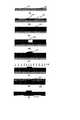
(実施例1)
本発明の一実施例を図1によって説明する。外形250mm角の銅張りポリイミドフィルム(日立化成工業(株)製:商品名MCF5000−I)11(a)の銅箔上に第一のレジストパターン12を形成し(b)、公知のサブトラクト法により所定の配線パターン13を形成後、第一のレジストパターンを剥離した(c)。次に、ポリイミド面からマスクイメージ法で波長248nmのKrFエキシマレーザを所定の位置に照射し、配線パターン13に達する凹部(直径30μm)14を形成した(d)。用いたエキシマレーザは、0.2μm/パルスの加工速度であるので、必要な加工深さはパルス数を制御することにより得られる。この場合は、約150パルスで所定の部分の配線パターンを露出させることができた。次に、配線パターン13面に第二のレジストパターン15を形成後、硫酸銅めっきにより凹部底(レーザ照射により露出した銅箔面)からポリイミド層表面以上のめっき柱16を形成した(e)。次に、めっき柱頭頂部及びポリイミド表面を研磨してめっき柱頭頂部及びポリイミド表面を平坦化した後、全面にエキシマレーザ光17を照射して(f)金属めっき柱をポリイミド表面から10μmだけ突出させた(g)。最後に、第二のレジストパターン15を剥離した後、腐食防止用表面仕上として厚さ0.2μmの無電解パターン金めっき18を施した。この場合、金属めっき柱頭頂部径dは設計値に対して±2μm以内であった。Example 1
An embodiment of the present invention will be described with reference to FIG. A
(実施例2)
本発明の一実施例を図2によって説明する。外形250mm角、厚さ35μmの電解銅箔21(日本電解(株)製:商品名SLP−12)上に厚さ0.5μmのニッケル薄層22を形成した(a)。次に、ドライフィルムレジスト(日立化成工業(株)製:商品名HS−415ED)をラミネートし、公知の露光・現像により所望する第一のレジストパターン23を形成した。次に、硫酸銅めっきにより電流密3.0A/dm2で配線パターン24を形成した(b)。次に、第一のレジストパターン23を3.0wt%の水酸化カリウム溶液で剥離した後、ポリイミドカバーレイ25(ニッカン工業(株)製:商品名CUSV−2035)の接着剤面を配線パターン面に向かい合わせて170℃、30kgf/cm2で60分間加熱加圧することにより配線パターンと積層した(c)。続いて、カバーレイ側からマスクイメージ法で波長248nmのKrFエキシマレーザを所定の位置に照射し、配線パターン24に達する凹部(直径30μm)26を形成した(d)。用いたエキシマレーザは、0.2μm/パルスの加工速度であるので、必要な加工深さはパルス数を制御することにより得られる。この場合は、約300パルスで所定の部分の配線パターンを露出させることができた。次に、硫酸銅めっきにより露出した配線パターン面からカバーレイ表面以上のめっき柱27を形成した(e)。次に、めっき柱頭頂部及びカバーレイ表面を研磨してめっき柱頭頂部及びカバーレイ表面を平坦化した後、全面にエキシマレーザ光8を照射して金属めっき柱をカバーレイ表面から10μmだけ突出させた(f)。次に、研磨面に第二のレジストパターン29を形成した後、アルカリエッチャント(メルテックス社製:商品名 Aプロセス)で露出している銅箔21を、続いて、ニッケル薄層22をニッケルエッチング液(メルテックス社製:商品名メルストリップ)によりエッチングして配線パターン24を露出させるとともに、接続端子部30を形成した。最後に、第二のレジストパターン29を剥離した後、腐食防止用表面仕上として厚さ0.2μmの無電解パターン金めっき31を施した。(Example 2)
An embodiment of the present invention will be described with reference to FIG. A nickel
11.銅張りポリイミドフィルム
12.第一のレジストパターン
13.配線パターン
14.凹部
15.第二のレジストパターン
16.めっき金属柱
17.レーザ光
18.パターン金めっき
21.銅箔
22.金属薄層
23.第一のレジストパターン
24.配線パターン
25.ポリイミドカバーレイ
26.凹部
27.めっき金属柱
28.レーザ光
29.第二のレジストパターン
30.接続端子部
31.パタ−ン金めっき
11. Copper-
Claims (1)
Translated fromJapanese前記金属箔をエッチングして配線パターンを形成した後、前記エッチングレジストパターンを剥離する工程、
前記ポリイミドフィルム側から前記配線パターンに達する凹部を、紫外領域に発振波長を有するエキシマレーザ光を照射することにより、所定の位置に形成する工程、
前記配線パターン面にめっきレジストを形成した後、電気めっき法により前記凹部底からポリイミドフィルム表面以上の金属柱を形成する工程、
前記ポリイミドフィルム及び前記金属柱の所定量を研磨して、前記ポリイミドフィルム表面及び前記金属柱頭頂部を平坦化する工程、
紫外領域に発振波長を有するエキシマレーザ光を研磨面の全面に照射し、所望する厚さの前記ポリイミドフィルムを選択的に除去して前記金属柱の所望する部分を前記ポリイミドフィルム表面から10μmだけ突出させる工程、および
前記めっきレジストを剥離する工程、
を有することを特徴とする接続部材の製造方法。Forming an etching resist pattern on the metal foil of the metal foil-cladpolyimide film ,
After the metal foil is etched to form a wiring pattern, the etching resist pattern is peeled off,
A step of forming a recess reaching the wiring pattern from thepolyimide film side ata predetermined positionby irradiating an excimer laser beam having an oscillation wavelength in the ultraviolet region ,
After forming a plating resist on the wiring pattern surface, a step of forming a metal column above thepolyimide film surface from the bottom of the recess by electroplating,
Step thepolyimide film and polishing the predetermined amount of the metal pillar, planarizing the surface of thepolyimide film and the metal column top part,
Excimer laser light having an oscillation wavelength in the ultraviolet region is irradiated onthe entire surfaceof the polished surface, and thepolyimide film having a desired thickness is selectively removed to project a desired portion of the metal pillar by10 μm from thepolyimide film surface. And a step of removing the plating resist,
The manufacturing method of the connection member characterized by having.
Priority Applications (1)
| Application Number | Priority Date | Filing Date | Title |
|---|---|---|---|
| JP2006127663AJP4388029B2 (en) | 2006-05-01 | 2006-05-01 | Manufacturing method of connecting member |
Applications Claiming Priority (1)
| Application Number | Priority Date | Filing Date | Title |
|---|---|---|---|
| JP2006127663AJP4388029B2 (en) | 2006-05-01 | 2006-05-01 | Manufacturing method of connecting member |
Related Parent Applications (1)
| Application Number | Title | Priority Date | Filing Date |
|---|---|---|---|
| JP03817895ADivisionJP3873294B2 (en) | 1995-02-27 | 1995-02-27 | Manufacturing method of connecting member |
Publications (2)
| Publication Number | Publication Date |
|---|---|
| JP2006284594A JP2006284594A (en) | 2006-10-19 |
| JP4388029B2true JP4388029B2 (en) | 2009-12-24 |
Family
ID=37406635
Family Applications (1)
| Application Number | Title | Priority Date | Filing Date |
|---|---|---|---|
| JP2006127663AExpired - LifetimeJP4388029B2 (en) | 2006-05-01 | 2006-05-01 | Manufacturing method of connecting member |
Country Status (1)
| Country | Link |
|---|---|
| JP (1) | JP4388029B2 (en) |
Family Cites Families (6)
| Publication number | Priority date | Publication date | Assignee | Title |
|---|---|---|---|---|
| JPH0680713B2 (en)* | 1989-10-11 | 1994-10-12 | 三菱電機株式会社 | Wafer test probe card and method of manufacturing the same |
| US5160779A (en)* | 1989-11-30 | 1992-11-03 | Hoya Corporation | Microprobe provided circuit substrate and method for producing the same |
| JP3057206B2 (en)* | 1991-03-27 | 2000-06-26 | キヤノン株式会社 | Electrical connection member and method of manufacturing the same |
| JP2981057B2 (en)* | 1992-07-07 | 1999-11-22 | 日東電工株式会社 | Flexible printed circuit board for hard disk driver |
| JPH06204651A (en)* | 1992-12-28 | 1994-07-22 | Canon Inc | Connecting method for electric circuit component to circuit board |
| JPH06347480A (en)* | 1993-06-04 | 1994-12-22 | Nitto Denko Corp | Probe structure |
- 2006
- 2006-05-01JPJP2006127663Apatent/JP4388029B2/ennot_activeExpired - Lifetime
Also Published As
| Publication number | Publication date |
|---|---|
| JP2006284594A (en) | 2006-10-19 |
Similar Documents
| Publication | Publication Date | Title |
|---|---|---|
| JP2730357B2 (en) | Electronic component mounted connector and method of manufacturing the same | |
| JP2023126229A (en) | Glass device intermediate | |
| US20180310417A1 (en) | Circuit board structure and method for forming the same | |
| WO2007058147A1 (en) | Printed wiring board, method for manufacturing same and use of same | |
| CN101112141A (en) | Multi-layer printed wiring board and manufacturing method thereof | |
| JPH11133062A (en) | Probe card and method for forming it | |
| JPH11145172A (en) | Bump structural body and forming method therefor | |
| JP2023081264A (en) | Method for manufacturing multilayer wiring board | |
| JP2005197649A (en) | Method for forming bump pad of flip chip and structure thereof | |
| JPH0917828A (en) | Circuit board | |
| US6562250B1 (en) | Method for manufacturing wiring circuit boards with bumps and method for forming bumps | |
| JP4388029B2 (en) | Manufacturing method of connecting member | |
| JP2002118204A (en) | Semiconductor device, substrate for mounting semiconductor and method for manufacturing the same | |
| JP3873294B2 (en) | Manufacturing method of connecting member | |
| JP2977124B2 (en) | Circuit board, manufacturing method thereof, and bump type contact head using the circuit board | |
| JP2009272571A (en) | Printed circuit board and method of manufacturing the same | |
| KR20090071494A (en) | Manufacturing Method of Printed Wiring Board | |
| JP2013058545A (en) | Electronic device and manufacturing method of the same | |
| KR20100111858A (en) | Method of fabricating a metal bump for printed circuit board | |
| JPH08235935A (en) | Anisotropic conductive film | |
| JP4246558B2 (en) | Wiring substrate for probe and method for manufacturing semiconductor element | |
| JP4190857B2 (en) | Printed circuit board connection method and composite printed circuit board | |
| CN114375496A (en) | Electronic interconnects defined by conductive paste lithography | |
| JP2006038457A (en) | Film probe manufacturing method | |
| KR100752016B1 (en) | Manufacturing method of printed circuit board |
Legal Events
| Date | Code | Title | Description |
|---|---|---|---|
| A131 | Notification of reasons for refusal | Free format text:JAPANESE INTERMEDIATE CODE: A131 Effective date:20071218 | |
| A02 | Decision of refusal | Free format text:JAPANESE INTERMEDIATE CODE: A02 Effective date:20080408 | |
| A521 | Written amendment | Free format text:JAPANESE INTERMEDIATE CODE: A523 Effective date:20080606 | |
| A911 | Transfer of reconsideration by examiner before appeal (zenchi) | Free format text:JAPANESE INTERMEDIATE CODE: A911 Effective date:20080729 | |
| A912 | Removal of reconsideration by examiner before appeal (zenchi) | Free format text:JAPANESE INTERMEDIATE CODE: A912 Effective date:20090206 | |
| A01 | Written decision to grant a patent or to grant a registration (utility model) | Free format text:JAPANESE INTERMEDIATE CODE: A01 | |
| A61 | First payment of annual fees (during grant procedure) | Free format text:JAPANESE INTERMEDIATE CODE: A61 Effective date:20091001 | |
| R150 | Certificate of patent or registration of utility model | Free format text:JAPANESE INTERMEDIATE CODE: R150 | |
| FPAY | Renewal fee payment (event date is renewal date of database) | Free format text:PAYMENT UNTIL: 20121009 Year of fee payment:3 |