JP4384410B2 - Thin film manufacturing method on special substrate and its application - Google Patents
Thin film manufacturing method on special substrate and its applicationDownload PDFInfo
- Publication number
- JP4384410B2 JP4384410B2JP2002570292AJP2002570292AJP4384410B2JP 4384410 B2JP4384410 B2JP 4384410B2JP 2002570292 AJP2002570292 AJP 2002570292AJP 2002570292 AJP2002570292 AJP 2002570292AJP 4384410 B2JP4384410 B2JP 4384410B2
- Authority
- JP
- Japan
- Prior art keywords
- manufacturing
- substrate
- component
- layer
- additional layer
- Prior art date
- Legal status (The legal status is an assumption and is not a legal conclusion. Google has not performed a legal analysis and makes no representation as to the accuracy of the status listed.)
- Expired - Lifetime
Links
- 239000000758substrateSubstances0.000titleclaimsabstractdescription166
- 238000004519manufacturing processMethods0.000titleclaimsabstractdescription55
- 239000010409thin filmSubstances0.000titleclaimsdescription41
- 238000000926separation methodMethods0.000claimsabstractdescription41
- 239000000463materialSubstances0.000claimsabstractdescription25
- 239000010410layerSubstances0.000claimsdescription117
- 238000000034methodMethods0.000claimsdescription48
- 239000011521glassSubstances0.000claimsdescription24
- 229920003023plasticPolymers0.000claimsdescription18
- VYPSYNLAJGMNEJ-UHFFFAOYSA-NSilicium dioxideChemical compoundO=[Si]=OVYPSYNLAJGMNEJ-UHFFFAOYSA-N0.000claimsdescription17
- 239000004033plasticSubstances0.000claimsdescription16
- 238000012545processingMethods0.000claimsdescription16
- 229910021420polycrystalline siliconInorganic materials0.000claimsdescription11
- 239000007789gasSubstances0.000claimsdescription9
- 238000010438heat treatmentMethods0.000claimsdescription9
- 229910052814silicon oxideInorganic materials0.000claimsdescription9
- 239000005350fused silica glassSubstances0.000claimsdescription8
- 239000011159matrix materialSubstances0.000claimsdescription8
- 229910052710siliconInorganic materials0.000claimsdescription8
- 239000010703siliconSubstances0.000claimsdescription8
- 239000001257hydrogenSubstances0.000claimsdescription7
- 229910052739hydrogenInorganic materials0.000claimsdescription7
- 238000000151depositionMethods0.000claimsdescription6
- 239000010408filmSubstances0.000claimsdescription6
- 239000011241protective layerSubstances0.000claimsdescription6
- UFHFLCQGNIYNRP-UHFFFAOYSA-NHydrogenChemical compound[H][H]UFHFLCQGNIYNRP-UHFFFAOYSA-N0.000claimsdescription5
- GNPVGFCGXDBREM-UHFFFAOYSA-Ngermanium atomChemical compound[Ge]GNPVGFCGXDBREM-UHFFFAOYSA-N0.000claimsdescription5
- 238000005520cutting processMethods0.000claimsdescription4
- 230000008021depositionEffects0.000claimsdescription4
- 230000003287optical effectEffects0.000claimsdescription4
- 230000008569processEffects0.000claimsdescription4
- 239000000126substanceSubstances0.000claimsdescription4
- 230000000295complement effectEffects0.000claimsdescription3
- 230000008878couplingEffects0.000claimsdescription3
- 238000010168coupling processMethods0.000claimsdescription3
- 238000005859coupling reactionMethods0.000claimsdescription3
- 229910052732germaniumInorganic materials0.000claimsdescription3
- 239000001307heliumSubstances0.000claimsdescription3
- 229910052734heliumInorganic materials0.000claimsdescription3
- SWQJXJOGLNCZEY-UHFFFAOYSA-Nhelium atomChemical compound[He]SWQJXJOGLNCZEY-UHFFFAOYSA-N0.000claimsdescription3
- 239000000203mixtureSubstances0.000claimsdescription3
- 230000010070molecular adhesionEffects0.000claimsdescription3
- 239000004065semiconductorSubstances0.000claimsdescription3
- 229910000927Ge alloyInorganic materials0.000claimsdescription2
- 229910000676Si alloyInorganic materials0.000claimsdescription2
- 239000011248coating agentSubstances0.000claimsdescription2
- 238000000576coating methodMethods0.000claimsdescription2
- 230000000694effectsEffects0.000claimsdescription2
- 229910052756noble gasInorganic materials0.000claimsdescription2
- 238000001953recrystallisationMethods0.000claimsdescription2
- 230000002441reversible effectEffects0.000claimsdescription2
- 238000010276constructionMethods0.000claims1
- 150000002431hydrogenChemical class0.000claims1
- 150000002835noble gasesChemical class0.000claims1
- 238000002360preparation methodMethods0.000abstractdescription4
- 238000010494dissociation reactionMethods0.000abstract1
- 230000005593dissociationsEffects0.000abstract1
- 238000012546transferMethods0.000description18
- 239000003351stiffenerSubstances0.000description7
- 238000005516engineering processMethods0.000description6
- XUIMIQQOPSSXEZ-UHFFFAOYSA-NSiliconChemical compound[Si]XUIMIQQOPSSXEZ-UHFFFAOYSA-N0.000description5
- 230000008901benefitEffects0.000description5
- 230000015572biosynthetic processEffects0.000description5
- 238000002513implantationMethods0.000description5
- 229920005591polysiliconPolymers0.000description4
- 229910021417amorphous siliconInorganic materials0.000description3
- 238000002347injectionMethods0.000description3
- 239000007924injectionSubstances0.000description3
- 230000010354integrationEffects0.000description3
- 150000002500ionsChemical class0.000description3
- 238000007725thermal activationMethods0.000description3
- 229910004298SiO 2Inorganic materials0.000description2
- 239000000853adhesiveSubstances0.000description2
- 230000001070adhesive effectEffects0.000description2
- 238000013459approachMethods0.000description2
- 239000011324beadSubstances0.000description2
- 239000000919ceramicSubstances0.000description2
- 239000013078crystalSubstances0.000description2
- 238000005468ion implantationMethods0.000description2
- 238000004377microelectronicMethods0.000description2
- 229910021421monocrystalline siliconInorganic materials0.000description2
- 230000036961partial effectEffects0.000description2
- 229920000642polymerPolymers0.000description2
- 229910052581Si3N4Inorganic materials0.000description1
- 229910000577Silicon-germaniumInorganic materials0.000description1
- 238000004026adhesive bondingMethods0.000description1
- 230000002411adverseEffects0.000description1
- 230000008859changeEffects0.000description1
- 238000007796conventional methodMethods0.000description1
- 230000000593degrading effectEffects0.000description1
- 230000001419dependent effectEffects0.000description1
- 230000006866deteriorationEffects0.000description1
- 229910003460diamondInorganic materials0.000description1
- 239000010432diamondSubstances0.000description1
- 238000009792diffusion processMethods0.000description1
- 230000002349favourable effectEffects0.000description1
- 238000011049fillingMethods0.000description1
- -1hydrogen ionsChemical class0.000description1
- GPRLSGONYQIRFK-UHFFFAOYSA-NhydronChemical compound[H+]GPRLSGONYQIRFK-UHFFFAOYSA-N0.000description1
- 238000002955isolationMethods0.000description1
- 239000007788liquidSubstances0.000description1
- 239000004973liquid crystal related substanceSubstances0.000description1
- 230000000873masking effectEffects0.000description1
- 239000012528membraneSubstances0.000description1
- 230000001681protective effectEffects0.000description1
- 230000035939shockEffects0.000description1
- HQVNEWCFYHHQES-UHFFFAOYSA-Nsilicon nitrideChemical compoundN12[Si]34N5[Si]62N3[Si]51N64HQVNEWCFYHHQES-UHFFFAOYSA-N0.000description1
- 125000006850spacer groupChemical group0.000description1
- 230000001502supplementing effectEffects0.000description1
Images


Classifications
- H—ELECTRICITY
- H01—ELECTRIC ELEMENTS
- H01L—SEMICONDUCTOR DEVICES NOT COVERED BY CLASS H10
- H01L21/00—Processes or apparatus adapted for the manufacture or treatment of semiconductor or solid state devices or of parts thereof
- H01L21/67—Apparatus specially adapted for handling semiconductor or electric solid state devices during manufacture or treatment thereof; Apparatus specially adapted for handling wafers during manufacture or treatment of semiconductor or electric solid state devices or components ; Apparatus not specifically provided for elsewhere
- H01L21/683—Apparatus specially adapted for handling semiconductor or electric solid state devices during manufacture or treatment thereof; Apparatus specially adapted for handling wafers during manufacture or treatment of semiconductor or electric solid state devices or components ; Apparatus not specifically provided for elsewhere for supporting or gripping
- H01L21/6835—Apparatus specially adapted for handling semiconductor or electric solid state devices during manufacture or treatment thereof; Apparatus specially adapted for handling wafers during manufacture or treatment of semiconductor or electric solid state devices or components ; Apparatus not specifically provided for elsewhere for supporting or gripping using temporarily an auxiliary support
- H—ELECTRICITY
- H01—ELECTRIC ELEMENTS
- H01L—SEMICONDUCTOR DEVICES NOT COVERED BY CLASS H10
- H01L21/00—Processes or apparatus adapted for the manufacture or treatment of semiconductor or solid state devices or of parts thereof
- H01L21/70—Manufacture or treatment of devices consisting of a plurality of solid state components formed in or on a common substrate or of parts thereof; Manufacture of integrated circuit devices or of parts thereof
- H01L21/71—Manufacture of specific parts of devices defined in group H01L21/70
- H01L21/76—Making of isolation regions between components
- H01L21/762—Dielectric regions, e.g. EPIC dielectric isolation, LOCOS; Trench refilling techniques, SOI technology, use of channel stoppers
- H01L21/7624—Dielectric regions, e.g. EPIC dielectric isolation, LOCOS; Trench refilling techniques, SOI technology, use of channel stoppers using semiconductor on insulator [SOI] technology
- H01L21/76251—Dielectric regions, e.g. EPIC dielectric isolation, LOCOS; Trench refilling techniques, SOI technology, use of channel stoppers using semiconductor on insulator [SOI] technology using bonding techniques
- H01L21/76254—Dielectric regions, e.g. EPIC dielectric isolation, LOCOS; Trench refilling techniques, SOI technology, use of channel stoppers using semiconductor on insulator [SOI] technology using bonding techniques with separation/delamination along an ion implanted layer, e.g. Smart-cut, Unibond
- H—ELECTRICITY
- H01—ELECTRIC ELEMENTS
- H01L—SEMICONDUCTOR DEVICES NOT COVERED BY CLASS H10
- H01L2221/00—Processes or apparatus adapted for the manufacture or treatment of semiconductor or solid state devices or of parts thereof covered by H01L21/00
- H01L2221/67—Apparatus for handling semiconductor or electric solid state devices during manufacture or treatment thereof; Apparatus for handling wafers during manufacture or treatment of semiconductor or electric solid state devices or components; Apparatus not specifically provided for elsewhere
- H01L2221/683—Apparatus for handling semiconductor or electric solid state devices during manufacture or treatment thereof; Apparatus for handling wafers during manufacture or treatment of semiconductor or electric solid state devices or components; Apparatus not specifically provided for elsewhere for supporting or gripping
- H01L2221/68304—Apparatus for handling semiconductor or electric solid state devices during manufacture or treatment thereof; Apparatus for handling wafers during manufacture or treatment of semiconductor or electric solid state devices or components; Apparatus not specifically provided for elsewhere for supporting or gripping using temporarily an auxiliary support
- H01L2221/68368—Apparatus for handling semiconductor or electric solid state devices during manufacture or treatment thereof; Apparatus for handling wafers during manufacture or treatment of semiconductor or electric solid state devices or components; Apparatus not specifically provided for elsewhere for supporting or gripping using temporarily an auxiliary support used in a transfer process involving at least two transfer steps, i.e. including an intermediate handle substrate
- H—ELECTRICITY
- H01—ELECTRIC ELEMENTS
- H01L—SEMICONDUCTOR DEVICES NOT COVERED BY CLASS H10
- H01L2924/00—Indexing scheme for arrangements or methods for connecting or disconnecting semiconductor or solid-state bodies as covered by H01L24/00
- H01L2924/30—Technical effects
- H01L2924/301—Electrical effects
- H01L2924/30105—Capacitance
- Y—GENERAL TAGGING OF NEW TECHNOLOGICAL DEVELOPMENTS; GENERAL TAGGING OF CROSS-SECTIONAL TECHNOLOGIES SPANNING OVER SEVERAL SECTIONS OF THE IPC; TECHNICAL SUBJECTS COVERED BY FORMER USPC CROSS-REFERENCE ART COLLECTIONS [XRACs] AND DIGESTS
- Y10—TECHNICAL SUBJECTS COVERED BY FORMER USPC
- Y10S—TECHNICAL SUBJECTS COVERED BY FORMER USPC CROSS-REFERENCE ART COLLECTIONS [XRACs] AND DIGESTS
- Y10S438/00—Semiconductor device manufacturing: process
- Y10S438/96—Porous semiconductor
Landscapes
- Engineering & Computer Science (AREA)
- Microelectronics & Electronic Packaging (AREA)
- Condensed Matter Physics & Semiconductors (AREA)
- General Physics & Mathematics (AREA)
- Manufacturing & Machinery (AREA)
- Computer Hardware Design (AREA)
- Physics & Mathematics (AREA)
- Power Engineering (AREA)
- Thin Film Transistor (AREA)
- Laminated Bodies (AREA)
- Crystals, And After-Treatments Of Crystals (AREA)
- Polymers With Sulfur, Phosphorus Or Metals In The Main Chain (AREA)
- Glass Compositions (AREA)
Abstract
Description
Translated fromJapanese本発明は、特殊基板における薄膜製造方法およびその適用に関する。 The present invention relates to a method for manufacturing a thin film on a special substrate and its application.
将来の携帯システム(たとえば携帯電話、チップカード、あるいはまた将来の携帯情報端末)は、ますます多機能を搭載するようになる見込みである。たとえば将来の携帯情報端末等の携帯システムの実現には、多数の技術的な「単位装置(brique)」が必要である。こうした技術的な単位装置の中には、スクリーン、オペレーティングシステム、マイクロプロセッサ、バッテリーが挙げられる。これらの構成部品の中で、スクリーンは大きな面積を占有し、システムへのスクリーンの集積は重要なポイントである。 Future mobile systems (eg, mobile phones, chip cards, or even future personal digital assistants) are likely to be equipped with more and more functions. For example, in order to realize a portable system such as a portable information terminal in the future, a number of technical “units” are necessary. Among these technical unit devices are screens, operating systems, microprocessors and batteries. Among these components, the screen occupies a large area, and the integration of the screen into the system is an important point.
こうした対象は、構成部品のコストが低い場合のみ大規模に開発される。そのためには、たとえばガラス等の大型基板に、これらの構成部品を形成可能にする大容量技術を持つことが必要である。しかし、この基板は、安価であるが衝撃に弱いという主要な欠点を有する。そこで、これらの基板に形成される構成部品または装置には、携帯システムに集積可能にするための追加保護手段を用いなければならない。 Such objects are developed on a large scale only when the cost of the components is low. For this purpose, it is necessary to have a large-capacity technology that enables these components to be formed on a large substrate such as glass. However, this substrate has the major drawback of being inexpensive but vulnerable to shock. Thus, additional protection means must be used for components or devices formed on these substrates to enable integration in portable systems.
ところで、こうした構成部品の集積化を最大にするには、最終基板にこれらの構成部品を集積することが有効であるように思われる。多くの場合、基板がプラスチック製であることが有利である。一つの試みは、たとえば、低価格、軽量、および良好な衝撃強さ(少なくともガラスに比べて)を併せ持つプラスチック基板上でスクリーンを得ることにある。この適用は、新世代の携帯電話には特に有効である。 By the way, in order to maximize the integration of these components, it seems effective to integrate these components on the final substrate. In many cases it is advantageous for the substrate to be made of plastic. One attempt is, for example, to obtain a screen on a plastic substrate that combines low cost, light weight, and good impact strength (at least compared to glass). This application is particularly effective for new generation mobile phones.
たとえばチップカード等の携帯システムの場合、さらに、(チップカードに適合させるための)重量の問題および柔軟性の問題から、構成部品の厚みを薄くすることが必要である。 For example, in the case of a portable system such as a chip card, it is further necessary to reduce the thickness of the component due to weight and flexibility issues (to fit the chip card).
(解決すべき問題点)
プラスチック等の基板にこれらの構成部品を形成することは、難しい問題である。事実、従来のプラスチックに適合するように構成部品の製造技術全体を変えるか、技術上の熱処理に適した特別な「プラスチック」基板を見出すかしなければならない(実際には、特に、基板の軟化点に達してはならないことは明らかである)。(Problem to be solved)
Forming these components on a substrate such as plastic is a difficult problem. In fact, we have to either change the overall manufacturing technology of the components to match conventional plastics or find a special “plastic” substrate suitable for technical heat treatment (in particular, softening of the substrate in particular) Obviously the point must not be reached).
別のアプローチは、既存の技術に適合する基板に構成部品(IC、スクリーン、パッシブ構成部品)を形成し、これを最終基板に移転することからなる。 Another approach consists of forming components (IC, screen, passive components) on a substrate that is compatible with existing technology and transferring it to the final substrate.
このアプローチは、概して、標準的なマイクロエレクトロニクス技術よりも簡単な技術により、低価格な基板に幾つかの構成部品を形成できるという長所がある。たとえば、アモルファスシリコンまたは多結晶シリコンからなる薄膜トランジスタ(略号TFT)等の、フラットスクリーンの製造に用いられる技術を挙げることができる。こうした技術は、一般にガラスからなる基板で実施される。 This approach generally has the advantage that several components can be formed on a low cost substrate with simpler technology than standard microelectronics technology. For example, the technique used for manufacture of flat screens, such as a thin film transistor (abbreviation TFT) which consists of amorphous silicon or polycrystalline silicon, can be mentioned. Such techniques are generally performed on substrates made of glass.
基板から別の基板に層を移転するには、さまざまな技術を用いることができる。たとえば、T.Hamaguchiらにより1985年に公表されたProc.IEDM1985(688ページ)の技術を挙げることができる。これらの技術は、一つの基板から別の基板に一つの層を有効に移転可能にするので、非常に有効である。しかし、ベース基板の消費(方法の間で破壊される)を要し、基板の消費を妨げるために停止層が存在する場合を除いて、薄膜を均質に(すなわち、全ての箇所において一定の厚みで)移転することができない。 Various techniques can be used to transfer a layer from one substrate to another. For example, T.W. Proc., Published in 1985 by Hamaguchi et al. The technology of IEDM 1985 (page 688) can be mentioned. These techniques are very effective because they enable one layer to be effectively transferred from one substrate to another. However, the thin film must be homogeneous (ie constant thickness at all points), unless it requires consumption of the base substrate (broken between methods) and there is a stop layer to prevent consumption of the substrate. Cannot be relocated).
最近になって、(ガラス基板上のポリシリコンからなる)TFTトランジスタを、プラスチック基板に移転する別の技術が紹介された。S.UtunomiyaらProc、IDS2000(916ページ)、またはSeikoによるEP−0924769Al参照。これらの方法は、(一般にはアモルファスシリコンからなる)分離層を基板に形成することに基づいており、この層に構成部品を形成後、分離を可能にし、別の基板への移転を可能にする。この場合、分離(または剥離)は、光(一般にレーザータイプビーム)による照射によって得られる。だが、このような照射は、大型面積の制御には難しい。実際、不均質な照射により剥離が不均質になり、表面膜の劣化を導くことがある。こうした技術的な悪条件は、無視できないものである。 Recently, another technique has been introduced for transferring TFT transistors (consisting of polysilicon on a glass substrate) to a plastic substrate. S. See Utunomia et al. Proc, IDS 2000 (page 916), or EP-09247769 Al by Seiko. These methods are based on forming a separation layer (generally made of amorphous silicon) on a substrate, allowing components to be separated after formation on this layer and allowing transfer to another substrate. . In this case, separation (or peeling) is obtained by irradiation with light (generally a laser type beam). However, such irradiation is difficult to control a large area. Actually, non-uniform irradiation may cause non-uniform peeling, leading to deterioration of the surface film. These technical adverse conditions cannot be ignored.
移転方法の中で、マイクロエレクトロニクス構成部品の全部または一部を含む材料、または含まない材料からなる薄膜の移転方法を用いることも同様に可能である。この方法は、一つまたは複数のガス種の導入によって、材料に埋められる脆い層を形成することに基づいている。こうした方法を紹介する、US−A−5374564(またはFR−A−2681472、またはEP−A−533551)、US−A−6020252(またはFR−A−2748851、またはEP−A−807970)、FR−A−2767416(またはEP−A−1010198)、FR−A−2748850(またはEP−A−902843)、またはFR−A−2773261(またはEP−A−9635598)を参照することができる。 In the transfer method, it is also possible to use a transfer method of a thin film made of a material including or not including all or part of the microelectronic component. This method is based on the formation of a brittle layer embedded in the material by the introduction of one or more gas species. US-A-5374564 (or FR-A-2681472 or EP-A-533551), US-A-6020252 (or FR-A-2748511, or EP-A-807970), FR-, which introduces such methods Reference may be made to A-2767416 (or EP-A-1010198), FR-A-2748850 (or EP-A-928443), or FR-A-2773261 (or EP-A-9635598).
一般に、上記の方法は、最初の基板の薄膜全体を剥がして、一定の基板に移転する目的で用いられる。その場合、得られた薄膜は基板の一部を含む。これらの薄膜は、電子構成部品または光構成部品を形成するための活性層の役割を果たすことができる。実際、こうした方法の主な長所は、異なる基板に単結晶基板の薄膜が得られることにある。薄膜は、構成部品の全部または一部を含むことが可能である。 In general, the above method is used for the purpose of peeling the entire thin film of the first substrate and transferring it to a certain substrate. In that case, the obtained thin film includes a part of the substrate. These thin films can serve as an active layer for forming electronic or optical components. In fact, the main advantage of such a method is that thin films of single crystal substrates can be obtained on different substrates. The thin film can include all or part of the components.
それに対して、こうした方法では、たとえばガラス、溶融シリカ、セラミック、幾つかのポリマー、および幾つかのアモルファス材料等の一定の基板における薄膜の分離が難しい。そのため、分離を行うには、実験条件を極端なものにすることが必要である。すなわち、注入量を非常に多くするか、および/または機械的な分離エネルギーを大きくすることが必要であるが、目下のところ、実際にこうした条件を検討することは難しい。 In contrast, such methods make it difficult to separate thin films on certain substrates such as glass, fused silica, ceramics, some polymers, and some amorphous materials. Therefore, in order to perform the separation, it is necessary to make the experimental conditions extreme. In other words, it is necessary to increase the injection amount and / or increase the mechanical separation energy, but it is difficult to actually examine these conditions at present.
ところで、ガラスは、多数の長所を備えた基板である。ガラスは安価であり、大型サイズでも存在し、取り扱いが簡単である。これは、フラットスクリーン用、カラーフィルタ用、または幾つかのパッシブ構成部品(R、L、C)用の、アクティブマトリクスおよび読み取り回路といった構成部品を製造する際に非常によく用いられる基板である。 By the way, glass is a substrate having many advantages. Glass is inexpensive, exists in large sizes, and is easy to handle. This is a substrate that is very often used in the production of components such as active matrices and reading circuits for flat screens, color filters, or some passive components (R, L, C).
かくして、本発明は、このタイプの基板に形成される構成部品を取り出して、別の支持体(たとえばプラスチック)または別の基板に移転することを目的とし、構成部品を形成して取り出すように、脆い層を最初の基板に形成する必要がない。 Thus, the present invention aims to take out the component formed on this type of substrate and transfer it to another support (eg plastic) or another substrate, so as to form and remove the component, There is no need to form a brittle layer on the first substrate.
一般に、本発明は、最初の基板に形成された構成部品または装置を別の基板に移転可能にし、上記の全ての方法の欠点(支持体の消費、不均質な移転、基板の特殊性)を持たない方法を目的とする。特に、本発明は、脆化される埋め込み層が容易に得られない基板に、一般に形成される構成部品または装置を回収可能にすること(構成部品の全てまたは一部を含む薄膜を回収後、基板をリサイクルして再利用可能にすること)、および、大型サイズ(数十センチメートル)で非常に均質な移転を実施可能にすることをめざしている。 In general, the present invention allows a component or device formed on the first substrate to be transferred to another substrate, and eliminates the disadvantages of all the above methods (consumer consumption, heterogeneous transfer, substrate peculiarities). The purpose is to have no method. In particular, the present invention makes it possible to recover a generally formed component or device on a substrate where an embrittled buried layer is not easily obtained (after recovering a thin film containing all or part of the component, It aims to make the substrate recyclable and reusable) and to enable a very homogeneous transfer in large sizes (tens of centimeters).
このため、本発明は、少なくとも構成部品の一部を組み込んだ薄膜の製造方法を提案し、この方法は、
少なくとも一部を局部的に脆化させることができる付加層を最初の基板に形成し、前記基板と前記脆化可能な部分とが、異なる材料からなり、および/または異なるミクロ構造を有する、準備ステップと、
この脆化可能な部分に脆い副層を生成する脆化ステップと、
前記付加層に少なくとも構成部品の全部または一部を形成する加工ステップと、
前記付加層の一部と前記構成部品の一部とを組み込んだ薄膜を得るために、前記脆化可能な部分が、前記脆い副層に沿って分離される分離ステップとを含む。For this reason, the present invention proposes a method of manufacturing a thin film incorporating at least a part of a component,
An additional layer that can be at least partially locally embrittled is formed on an initial substrate, the substrate and the embrittleable part being made of different materials and / or having different microstructures Steps,
An embrittlement step for generating a brittle sublayer in this embrittleable part;
A processing step of forming at least all or a part of the components in the additional layer;
In order to obtain a thin film incorporating a portion of the additional layer and a portion of the component, the embrittleable portion includes a separation step of separating along the fragile sublayer.
かくして、本発明は、構成部品の準備に関連する各種の基準に応じて自由に選択された基板に対して、構成部品を含む薄膜を分離可能にし、基板でこの分離を行うように構成する必要がない。 Thus, it is necessary for the present invention to be able to separate the thin film containing the component from the substrate freely selected according to various criteria related to the preparation of the component, and to perform this separation on the substrate. There is no.
本発明は、特に、後で行われる分離のための脆化層が容易に得られない基板に適している。そのため、本発明は、特に、基板が、半導体材料、ガラス、または溶融シリカからなる場合(他の材料は、特にセラミック、幾つかのポリマー、および幾つかのアモルファス材料など、同様の不利な条件を持つ。上記参照)、あるいは、付加層の存在により可能になる条件よりもずっと厳しい条件で、分離を可能にする基板に適している。 The present invention is particularly suitable for a substrate in which an embrittlement layer for subsequent separation is not easily obtained. Therefore, the present invention is particularly suitable when the substrate is made of a semiconductor material, glass, or fused silica (other materials have similar disadvantages, especially ceramics, some polymers, and some amorphous materials. Suitable for substrates that allow separation under conditions much more severe than those possible due to the presence of additional layers.
本発明は、特に、大型の薄膜が望ましい場合に適しており(もちろん、これは、基板が少なくとも同じサイズであると想定している)、この場合、実際には、すぐれた機械強度、特に、すぐれた剛性をもつ基板を用いなければならない。 The present invention is particularly suitable when large thin films are desired (which, of course, assumes that the substrates are at least the same size), in which case, in practice, excellent mechanical strength, in particular, A substrate with excellent rigidity must be used.
付加層は、様々な性質のものとすることができる。たとえば、(好適なケースでは)付加層が、シリコンからなり、さらにはゲルマニウム、またはシリコンとゲルマニウムとの合金からなる。付加層がシリコンである場合、好適には、単結晶シリコンよりも安価な多結晶シリコンとすることができる。 The additional layer can be of various properties. For example, (in the preferred case) the additional layer is made of silicon, and further consists of germanium or an alloy of silicon and germanium. When the additional layer is silicon, it can be preferably polycrystalline silicon that is cheaper than single crystal silicon.
脆化可能なこの部分は、有利には、堆積、次いで再結晶により形成される。しかし、US−5374564に記載されているような別の方法で形成してもよい。 This part that can be embrittled is advantageously formed by deposition followed by recrystallization. However, it may be formed by another method as described in US-5374564.
この脆化可能な部分の厚みは、一般に、少なくとも約50ナノメータであり、好適には約1000ナノメータ未満である。これにより、薄膜の底面の良好な平面性が得られる。 The thickness of the embrittleable portion is generally at least about 50 nanometers, and preferably less than about 1000 nanometers. Thereby, the favorable flatness of the bottom face of a thin film is obtained.
場合によっては、基板と脆化可能な部分との間に連結層を配置する。このため、基板がガラスまたは溶融シリカからなり、脆化可能な部分がシリコンからなる場合、場合によっては酸化シリコンからなる連結層がある。 In some cases, a connecting layer is disposed between the substrate and the brittle portion. For this reason, when the substrate is made of glass or fused silica and the brittle portion is made of silicon, there is a connecting layer made of silicon oxide in some cases.
本発明の有利な別の特徴によれば、付加層は、脆化可能な部分に、(組成、機械特性、化学特性等の観点から)基板の性質と同じかまたは類似する性質を備えた、構成部品(または構成部品の少なくとも一部)を受容する追加層を含む。基板がガラスまたは溶融シリカからなる場合、追加層は、有利には酸化シリコンからなる。 According to another advantageous characteristic of the invention, the additional layer has, in the embrittleable part, a property that is the same as or similar to that of the substrate (in terms of composition, mechanical properties, chemical properties, etc.) It includes an additional layer that receives the component (or at least a portion of the component). If the substrate is made of glass or fused silica, the additional layer is advantageously made of silicon oxide.
追加層は、脆化ステップの前または後に付加可能である。 Additional layers can be added before or after the embrittlement step.
かくして、本発明のこの特徴によれば、「準基板(quasi−substrate)」の内部に脆化層を形成する(脆化層は、二つの同じ材料または非常に類似した材料の間にサンドイッチ状に挟まれる)。準基板は、基板の全ての長所を有し(ガラスの場合、たとえば表面状態、アセンブリの剛性)、サンドイッチ状に挟まれた層で、ガス種の導入による脆化層の形成と容易に適合する。この「準基板」により、容易な分離に適さない基板に構成部品または装置を形成し、その後、これらを簡単に引き離して、別の基板に移転することができる。 Thus, according to this aspect of the invention, an embrittlement layer is formed within a “quasi-substrate” (the embrittlement layer is sandwiched between two identical or very similar materials). Between). The quasi-substrate has all the advantages of the substrate (in the case of glass, for example, the surface state, the rigidity of the assembly), and is sandwiched between layers, easily compatible with the formation of an embrittled layer by the introduction of gas species. . This “quasi-substrate” allows components or devices to be formed on a substrate that is not suitable for easy separation, after which they can be easily pulled apart and transferred to another substrate.
追加層の厚みは、好適には約300ナノメータから10000ナノメータであり、脆化処理を可能にするように十分に薄くするが、しかし、一つ(または複数)の構成部品を少なくとも部分的に適切に形成可能にするように、および/または薄膜を自己支持形とすることができるように、および/または構成部品の形成ステップ、脆化ステップ、または分離ステップ中に、ブリスターが現われることがないように、十分に有効な厚みにする。換言すれば、脆化可能な層と構成部品との間に配置される追加層は、得られる薄膜の補剛材の役割をすることができる。これによって、また、最終基板への移転前に薄膜を取り扱うことができ、一時的な基板が不要になる。 The thickness of the additional layer is preferably about 300 nanometers to 10,000 nanometers and is thin enough to allow embrittlement, but one (or more) components are at least partially suitable So that the film can be self-supporting and / or the blisters do not appear during the component forming, embrittlement or separation steps And a sufficiently effective thickness. In other words, the additional layer disposed between the embrittleable layer and the component can serve as a stiffener for the resulting thin film. This also allows the thin film to be handled before transfer to the final substrate, eliminating the need for a temporary substrate.
この追加層の厚みは、好適には、脆化可能な層の厚みよりも厚い(脆化可能な層の厚みと、追加層とに関する上記の理由による)。 The thickness of this additional layer is preferably greater than the thickness of the embrittleable layer (for the above reasons regarding the thickness of the embrittleable layer and the additional layer).
有利には、追加層の下に(追加層と脆化可能な層との間に)、構成部品を含む層と最終基板とを適合可能にする第三の層を設けることができる。第三の層は、たとえばSi3N4の層である。この場合、脆化ゾーンで破砕後、付加層の残留部分を除去し、Si3N4の層を露出する。Advantageously, a third layer can be provided below the additional layer (between the additional layer and the embrittleable layer) that allows the layer containing the component and the final substrate to be compatible. The third layer is, for example, a layer of Si3 N4 . In this case, after crushing in the embrittlement zone, the remaining portion of the additional layer is removed, and the Si3 N4 layer is exposed.
有利には、脆化ステップが、熱活性処理の実施を含む。特に、この処理は、好適には、脆化可能な層の深さでの元素の導入を含み、その後、元素の拡散により、熱条件に応じて所望の脆化を引き起こすことができる。 Advantageously, the embrittlement step comprises performing a thermal activation treatment. In particular, this treatment preferably involves the introduction of elements at the depth of the embrittleable layer, after which diffusion of the elements can cause the desired embrittlement depending on the thermal conditions.
このため、本発明の有利な特徴によれば、脆化ゾーンは、好適には水素および/またはヘリウムおよび/または希ガスの中から選択される、ガス種の導入により形成される。特に水素の使用が適している。ここでは、US−A−5374564(またはFR−A−2681472、またはEP−A−533551)、US−A−6020252(またはFR−A−2748851、またはEP−A−807970)、FR−A−2767416(またはEP−A−1010198)、FR−A−2748850(またはEP−A−902843)またはFR−A−2773261(またはEP−A−963598)を参照することができる。 Thus, according to an advantageous feature of the invention, the embrittlement zone is formed by the introduction of a gas species, preferably selected from hydrogen and / or helium and / or a noble gas. The use of hydrogen is particularly suitable. Here, US-A-5374564 (or FR-A-2681472 or EP-A-5335551), US-A-6020252 (or FR-A-2878551 or EP-A-807970), FR-A-2767416 (Or EP-A-1010198), FR-A-2748850 (or EP-A-902843) or FR-A-2773261 (or EP-A-963598).
こうした熱活性処理の場合、分離ステップは、好適には特別な熱エネルギー供給を含む。 In the case of such thermal activation treatment, the separation step preferably includes a special heat energy supply.
この熱エネルギー供給は、これを非常に有効にするために、少なくとも脆化可能な部分を、構成部品の製造ステップ中に既に供給された熱収支より大きい熱収支に至らせる効果がある。 This thermal energy supply has the effect that, in order to make this very effective, at least the part that can be embrittled leads to a heat balance that is greater than the heat balance already supplied during the component manufacturing steps.
分離処理は、上記の熱エネルギー供給と組み合わせて使用されるか、または単独で使用される機械エネルギー供給(この表現の最も広い意味で、すなわち、構造体に加えられる力または構造体にもたらされる応力として、一方でまた、たとえばガス導入等による気体としての)を含むことができる。 The separation process is used in combination with the thermal energy supply described above or used alone (in the broadest sense of this expression, ie the force applied to the structure or the stress exerted on the structure). On the other hand, it can also include (for example, as a gas by gas introduction etc.)
同一基板に複数の構成部品または装置を形成する一定の場合、1個の装置(または整数の複数装置)の寸法に対応する寸法のゾーンで、局部的な分離を行うことが有利である。 In certain cases where multiple components or devices are formed on the same substrate, it may be advantageous to perform local separation in zones whose dimensions correspond to the dimensions of a single device (or an integral number of devices).
好適には、本発明による方法は、あとで一緒に同一機能を果たすアクティブまたはパッシブ素子のアセンブリを形成することを目的とする。このようなアセンブリを一般に「装置」と呼ぶ。たとえば、装置は、光構成部品、光−電気構成部品、電子構成部品、カラーフィルタ、または機械、化学、および/または生物学センサ等を含むことができる。これは、また、アドレッシング回路(フラットスクリーンの場合)を備えたアクティブマトリクスであってもよい。従って、装置は、原則として1個以上の構成部品を含む。そのため、層に存在する構成部品は必ずしも同じではない。 Preferably, the method according to the invention is aimed at forming an assembly of active or passive elements which later perform the same function together. Such an assembly is generally referred to as an “apparatus”. For example, the device can include optical components, opto-electrical components, electronic components, color filters, or mechanical, chemical, and / or biological sensors and the like. This may also be an active matrix with an addressing circuit (in the case of a flat screen). Thus, the device comprises in principle one or more components. Thus, the components present in the layers are not necessarily the same.
かくして、製造ステップが、光構成部品または光−電気構成部品の製造を含み、および/または電子構成部品の製造を含み、および/または機械、化学、または生物学センサの製造を含むのに応じて、複数の(限定的ではない)個別的なケースを区別することができる。 Thus, depending on whether the manufacturing steps include the manufacture of optical components or opto-electrical components, and / or the manufacture of electronic components, and / or the manufacture of mechanical, chemical, or biological sensors Multiple (but not limited) individual cases can be distinguished.
特に有効なケースは、製造ステップが、その後フラットスクリーンに集積されるように構成された、少なくとも一つのアクティブマトリクス、およびそのアドレッシング回路の製造を少なくとも含むケースである。 A particularly effective case is one in which the manufacturing steps include at least the manufacture of at least one active matrix and its addressing circuit, which are then configured to be integrated on a flat screen.
本発明による方法は、また、加工ステップ後、構成部品を含む付加層に保護層を堆積する被覆ステップを含むことができる。保護層は、少なくともシリコンからなる付加層および/または酸化シリコンからなる追加層の場合、好適には、窒化シリコンSi3N4からなる。保護層は、最終基板との適合性を保証する役割を果たすことができる(例えば、プラスチック基板上で構成部品が劣化しないようにする)。The method according to the invention can also include a coating step, after the processing step, depositing a protective layer on the additional layer containing the component. In the case of at least an additional layer made of silicon and / or an additional layer made of silicon oxide, the protective layer is preferably made of silicon nitride Si3 N4 . The protective layer can serve to ensure compatibility with the final substrate (eg, keep components from degrading on plastic substrates).
1個の最終基板(または、薄膜が単独の最終基板用ではない場合は、複数の最終基板)に薄膜の全部または一部を移転する場合、中間基板を介在させてもさせなくてもよい。 When transferring all or part of the thin film to one final substrate (or a plurality of final substrates if the thin film is not for a single final substrate), an intermediate substrate may or may not be interposed.
さらに、本発明による方法は、分離ステップの前に、付加層(場合によっては、追加層を含む)に中間基板を固定する結合ステップを含み、分離ステップ後、この中間基板を用いて、一つ(または複数)の最終基板に薄膜の全部または一部を固定する移転ステップを含むことができる。 Furthermore, the method according to the invention comprises a bonding step for fixing the intermediate substrate to an additional layer (possibly including an additional layer) prior to the separation step, and using this intermediate substrate after the separation step, A transfer step may be included that secures all or part of the thin film to the (or more) final substrates.
好適には、この結合ステップ時に、中間基板に可逆的に薄膜を固定し、移転ステップ後、中間基板から薄膜を剥がす。中間基板からの薄膜の移転部分の引き離し、非常に容易であり、特別な処理は不要である。 Preferably, the thin film is reversibly fixed to the intermediate substrate during the bonding step, and after the transfer step, the thin film is peeled off from the intermediate substrate. The transfer part of the thin film from the intermediate substrate can be easily separated and no special treatment is required.
有利には、最終基板が、出発基板とは異なる材料からなる。特に、最終基板は、加工ステップまたは分離ステップの熱条件と相容れない材料から構成可能である。これにより、最終基板のための選択の余地が非常に広がる。かくして、有利には、たとえば加工ステップの最大温度より軟化温度を低くすることができる、透明なプラスチック材料から最終基板を構成可能である(従って、最終基板は、加工ステップに対して耐性がない)。実際、これは、全く有効なケースに対応する。 Advantageously, the final substrate is made of a different material than the starting substrate. In particular, the final substrate can be composed of a material that is incompatible with the thermal conditions of the processing or separation step. This greatly expands the choice for the final substrate. Thus, advantageously, the final substrate can be constructed from a transparent plastic material, for example, with a softening temperature that can be lower than the maximum temperature of the processing step (thus the final substrate is not resistant to the processing step). . In fact, this corresponds to a completely valid case.
このため、本発明は、この方法の、フラットスクリーンの製造への特定の適用を含む。 Thus, the present invention includes a specific application of this method to the manufacture of flat screens.
最終基板の寸法は、出発基板の寸法、従って得られる薄膜の寸法とは異なるものにしてもよい(必要に応じて大きくしたり小さくしたりする)ことに留意されたい。 Note that the dimensions of the final substrate may be different from the dimensions of the starting substrate and thus the resulting thin film (increase or decrease as necessary).
特に別の有利なケースでは、最終基板が、チップカードまたは移動電話の一部であり、さらには、自己支持形で柔軟なスクリーンのプラスチック偏光子である。 In another particularly advantageous case, the final substrate is part of a chip card or a mobile phone, and further is a self-supporting flexible screen plastic polarizer.
ここで注意することが大切なのは、加工ステップ時に、付加層または追加層に複数の構成部品を形成した場合、各構成部品を、薄膜の残りの部分から剥がしながら、特定の最終基板たとえばチップカードに、個々に固定可能であることである(これは、製造ステップが、複数ロットの補足する構成部品を形成することからなる場合にも、あてはまる。すなわち、各ロットを個々に堆積可能である)。 It is important to note that if multiple components are formed in the additional layer or additional layers during the processing step, each component is peeled off from the rest of the thin film and applied to a specific final substrate such as a chip card. (This also applies if the manufacturing step consists of forming complementary components of multiple lots, ie each lot can be deposited individually).
このような中間基板は、基板に対して薄膜を引き離す脆化部分で、機械応力を発生する役割を果たすことができる。 Such an intermediate substrate can play a role of generating mechanical stress at an embrittled portion that separates the thin film from the substrate.
さらに、出発基板とは別の最終基板に移転するためのこのような中間基板が、上記のケースでは、補剛材の機能を果たす十分に厚い追加層を必要としないことに注目すべきである。 Furthermore, it should be noted that such an intermediate substrate for transfer to a final substrate different from the starting substrate does not require a sufficiently thick additional layer to serve as a stiffener in the above case. .
本発明の方法の別の変形実施形態は、さらに、分離ステップの前に、最終基板に付加層(追加層がある場合には追加層を含めて)を固定する結合ステップを含むことからなる。この場合、構成部品は、最終基板上で、付加層におけるこれらの構成部品の構成とは逆の構成になる(移転が中間基板を介して行われる場合、構成部品の構成は維持される。この構成は薄膜が自己支持形であるとき、すなわち追加層が補剛材の役割を果たすとき、自由選択で維持もしくは逆転可能である)。 Another alternative embodiment of the method of the invention further comprises a bonding step of fixing an additional layer (including the additional layer, if any) to the final substrate prior to the separation step. In this case, the components are on the final substrate opposite to the configuration of these components in the additional layer (if the transfer takes place via the intermediate substrate, the configuration of the components is maintained. The configuration can be optionally maintained or reversed when the membrane is self-supporting, ie when the additional layer acts as a stiffener).
一つ(または複数の)構成部品は、あらゆる手段、特に、接着剤による貼り合わせあるいは分子接着により、薄膜の他の部分と共に、あるいは別に、固定可能である。 The component (s) can be fixed together with or separately from other parts of the thin film by any means, in particular by adhesive bonding or molecular adhesion.
本発明の目的、特徴、および長所は、添付図面に関して限定的ではなく例として挙げられた以下の説明から明らかになるであろう。 Objects, features, and advantages of the present invention will become apparent from the following description, given by way of example and not limitation with reference to the accompanying drawings.
図1から4は、本発明の方法を実施する例を一般的に示す。 1 to 4 generally show examples of implementing the method of the invention.
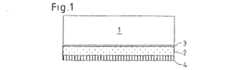
たとえばLCDスクリーンの製造に用いられるような大型のガラスプレート1を選ぶ。たとえば、CORNING社の整理番号1737と記載されたガラスにする。 For example, a
たとえば厚さ300nmのアモルファスシリコン層2を堆積し、たとえばレーザビームを用いてこれを再結晶化することにより、ポリシリコンとも呼ばれる多結晶シリコンを得る。後述するように、この層2は脆化可能である。単結晶シリコンを移転することもできるが、そうすると経済的な面で不利である。 For example, an
一定の場合、薄膜を引き離し可能にするこうした特別な層を形成する前に、接合を促す中間層3を基板に堆積することができる。この整合層3は、たとえば酸化シリコン層とすることができる。図1では、分かりやすくするために、この層の厚さを誇張してある。厚さは、わずか10ナノメータにすぎない。 In certain cases, an intermediate layer 3 that facilitates bonding can be deposited on the substrate prior to forming such a special layer that allows the film to be pulled apart. This matching layer 3 can be, for example, a silicon oxide layer. In FIG. 1, the thickness of this layer is exaggerated for clarity. The thickness is only 10 nanometers.
また、たとえば温度550℃でCVDタイプの堆積により、ポリシリコン層を得ることもできる。この変形実施形態は、基板が溶融シリカであり、この基板が堆積温度程度の温度に耐える場合、前の実施形態よりも好ましい場合がある。本発明の方法では、実施形態に応じて基板をリサイクルできる(消費されない)ので、価格が高い基板を用いてもよいことに留意されたい。 Further, for example, a polysilicon layer can be obtained by CVD type deposition at a temperature of 550 ° C. This variant embodiment may be preferred over the previous embodiment if the substrate is fused silica and the substrate can withstand temperatures as high as the deposition temperature. It should be noted that in the method of the present invention, the substrate can be recycled (not consumed) depending on the embodiment, so that a costly substrate may be used.
図示された例では、その後、たとえば数百ナノメータ(たとえば800nm)の酸化シリコン層4を堆積し、最初のガラスに近いSiO2タイプの自由面をもつようにする。その場合、準基板1+2+4が得られ、1と4は、非常に近い材料に相当する。In the example shown, a silicon oxide layer 4 of, for example, a few hundred nanometers (for example 800 nm) is then deposited so as to have a free surface of the SiO2 type close to the original glass. In that case, a
図2に示したように、層2に脆い副層5を生成する。このため、次に、熱活性化可能な処理を施す。好適には、イオンまたはガス種(最も軽いイオンが気体元素イオンである限り、双方は同じである)をポリシリコン層の深さに導入し、脆化層を形成して、これを後で引き離す。たとえば、ドーズ量約7E16H+/cm2、エネルギー100keVで水素を注入する。As shown in FIG. 2, a
これらの分離処理は、脆化ステップ(注入ドーズ量、エネルギー、注入温度など)に応じて適合される。 These separation processes are adapted according to the embrittlement step (implantation dose, energy, implantation temperature, etc.).
引き離し後、自己支持形の構造を得るように、厚さ3マイクロメータの酸化シリコン堆積物を付加してもよい(従って、考慮された例では層4が厚くなる)。この層は、薄膜製造方法において補剛材の役割を果たす。 After pulling, a 3 micrometer thick silicon oxide deposit may be added to obtain a self-supporting structure (thus, in the example considered, layer 4 is thicker). This layer serves as a stiffener in the thin film manufacturing method.
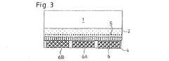
その後、SiO2の面に、装置の全部または一部、すなわち少なくとも一つの構成部品6を形成する(図3参照)(図3では、装置を共に形成可能な構成部品6、6A、6Bの3個の構成部品がある)。このステップは、全体がガラスからなる基板に構成部品を形成可能であるような、従来の条件で行われる。Thereafter, all or part of the device, that is, at least one
最終的にフラットスクリーンが望まれる場合、装置は、アクティブマトリクスとそのアドレッシング回路とのトランジスタユニットから構成可能である。一般に、約400℃を超える温度は、この技術では使用されない。 If a flat screen is ultimately desired, the device can consist of a transistor unit of an active matrix and its addressing circuit. In general, temperatures above about 400 ° C. are not used in this technique.
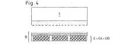
その後、移転を引き起こすために分離処理(引き離しまで進められる)を行う(図4参照)。一般に、このステップは、熱処理および/または機械処理を含むことができる。一定の場合、この分離は、第一の手段(たとえば熱処理)により開始され、その後、第二の手段(たとえば機械手段)によって裂くことにより、引き離しまで進められる。変形実施形態では、また、たとえば何分間か約450℃で熱処理を実施し、すべての層が熱処理に耐えることができる場合、分離、次いで引き離しを行う。分離条件および引き離し条件は、知られているように、注入条件に著しく応じる。 Thereafter, separation processing (proceeding to separation) is performed to cause relocation (see FIG. 4). In general, this step can include heat treatment and / or mechanical treatment. In certain cases, this separation is initiated by a first means (eg heat treatment) and then advanced to tearing by tearing by a second means (eg mechanical means). In an alternative embodiment, the heat treatment is also performed, for example, at about 450 ° C. for several minutes, and if all layers can withstand the heat treatment, separation and then pull-off are performed. Separation and pull-out conditions are highly dependent on injection conditions, as is known.
その場合、装置または構成部品6は、製造基板1+2から分離される。このように得られた薄膜に参照符号8を付した。構成部品間のスペースを保護材料で占有してもよい。 In that case, the device or
分離するとは、装置が依然として基板と接触していてもよいが、結合エネルギーが非常に弱い(たとえば静電保持力)ことを意味する。一方、引き離しとは、薄膜8が完全にその基板とは無関係になるまでの完全な分離を意味する。 Separation means that the device may still be in contact with the substrate, but the binding energy is very weak (eg, electrostatic holding force). On the other hand, separation means complete separation until the
前述のように、補剛材の役割を果たせるように追加層4を寸法決定する限り、薄膜が自己支持され、その操作には付加的な補剛材が不要である。従って、最終基板(図示せず)に構成部品を移転可能である。 As mentioned above, as long as the additional layer 4 is dimensioned to serve as a stiffener, the thin film is self-supported and no additional stiffener is required for its operation. Accordingly, the components can be transferred to the final substrate (not shown).
しかしながら、薄膜を自己支持形とみなすことができるにしても、装置または構成部品6を中間基板に接着させて、装置または構成部品を最終基板までもっと容易に操作可能にすることが好ましい場合がある。このような接着を行うには、材料、たとえば接着剤などの添加といったあらゆる手段、あるいは、表面調製(特に分子接着)の実施手段を用いることができる。 However, even though the film can be considered self-supporting, it may be preferable to adhere the device or
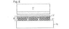
かくして、図5は、図3の基板と同様の基板を示しており、ガラス層1’と、脆化可能な層2’(場合によっては整合層3’を含む)と、構成部品6’、6A’、6B’を製造する追加層4’とを含む。さらに、有利には、図示していない保護層が堆積される。薄膜の引き離しを行う前に、構成部品を基板10に固定する。引き離し後(図6)、基板10が構成部品の操作を容易にする。 Thus, FIG. 5 shows a substrate similar to the substrate of FIG. 3, with a
そのため、図7で示されている基板の構成部品6’は、薄膜の残りの部分から剥がされて、最終基板12に個別に移転されている。 Therefore, the
別の任意選択は、構成部品を最終基板に直接接触させようとすることからなる。この場合、構成部品は、基板に留まるようにされる。 Another option consists in trying to bring the component directly into contact with the final substrate. In this case, the component is allowed to remain on the substrate.
もちろん、基板10は、一時的な基板の役割をするか最終基板の役割をするかに応じて、同じ組成も同じ特性も持たないようにすることができる。 Of course, the
中間基板を使用する場合、接着を可逆式にするように、この接着を制御可能である。かくして、装置をその最終基板に結合後、中間基板を除去可能である。 If an intermediate substrate is used, this adhesion can be controlled so that the adhesion is reversible. Thus, after bonding the device to its final substrate, the intermediate substrate can be removed.
従来技術の知られている文献に記載されたような方法を実施可能であり、すなわち、特に、表面剛性の制御または親水性の制御により、結合力を制御できることに留意すべきである。 It should be noted that methods such as those described in the known literature of the prior art can be implemented, i.e. the binding force can be controlled in particular by controlling the surface stiffness or the hydrophilicity.
最終基板に装置を移転後、最終基板に適合する従来の技術ステップを実施することにより、装置を補完できる。 After transferring the device to the final substrate, the device can be complemented by performing conventional technical steps that are compatible with the final substrate.
この方法の変形実施形態では、装置(6’+6A’+6B’)の形成後、機械的な力の使用(たとえばブレードの導入、液体流または気体流の使用など)によって、熱処理を補うことにより引き離しが行われる。中間基板10は、たとえばねじれ力の付与により、脆い副層に様々な力を発生する役割を果たすことができる。 In a variant embodiment of this method, after the formation of the device (6 ′ + 6A ′ + 6B ′), it is pulled apart by supplementing the heat treatment by the use of mechanical forces (eg introduction of blades, use of liquid or gas flow, etc.). Is done. The
このような引き離しは、埋められた脆い層が、水素注入(6E16H+/cm2、100keV) により得られた場合に実施可能である。たとえば温度300℃未満で装置を形成後、30分間、450℃で熱処理を実施して、脆いゾーンで著しい脆化を行う。この脆化は、熱活性化現象を介在させるので、各注入条件(エネルギー、ドーズ量)に対して時間と温度との組み合わせが存在する。Such detachment can be performed when the buried brittle layer is obtained by hydrogen implantation (6E16H+ / cm2 , 100 keV). For example, after forming the device at a temperature of less than 300 ° C., heat treatment is performed for 30 minutes at 450 ° C., and significant embrittlement is performed in the brittle zone. Since this embrittlement causes a thermal activation phenomenon, there is a combination of time and temperature for each implantation condition (energy, dose).
最終的には、引き離しを機械的に終了する。 Eventually, the separation is mechanically terminated.
上記の例では、脆化可能な層がシリコンからなる。変形実施形態では、また、脆化可能なこの層が、ゲルマニウム、SiGe、あるいはイオン注入により脆化可能な他のあらゆる材料(たとえば単結晶または多結晶半導体)から構成可能である。 In the above example, the brittle layer is made of silicon. In alternative embodiments, the layer that can be embrittled can also be composed of germanium, SiGe, or any other material that can be embrittled by ion implantation (eg, single crystal or polycrystalline semiconductor).
従って、本発明の方法を適用して、(第一の基板に全体として構成された)装置を、たとえばプラスチックタイプの第二の基板に移転することができる。かくして、従来の手段によりLCDスクリーンを完全に形成し、有利には柔軟な基板とすることができるプラスチック基板に、このスクリーンを最終的に移転可能である。 Thus, the method of the present invention can be applied to transfer the device (configured as a whole on the first substrate) to a second substrate, for example of the plastic type. Thus, the screen can finally be transferred to a plastic substrate, which can be completely formed by conventional means, advantageously a flexible substrate.
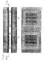
図8から17は、このような複数の各LCD構成部品の製造を示している。 Figures 8 to 17 illustrate the manufacture of such a plurality of LCD components.
要約すれば、このために2個のガラスプレートを選択するが、これはフラットスクリーンの製造では一般的である。1枚のプレートには、アクティブマトリクスのトランジスタとアドレッシング回路とを形成し、1枚のプレートには、カラーフィルタを形成する。2個の部分を組み立ててスクリーンを仕上げてから、ガラス基板を除去し、このスクリーンを最終基板に移転する。この方法の変形実施形態では、最終基板への移転後、スクリーンを仕上げることができる。 In summary, two glass plates are selected for this, which is common in flat screen manufacturing. An active matrix transistor and an addressing circuit are formed on one plate, and a color filter is formed on one plate. After assembling the two parts to finish the screen, the glass substrate is removed and the screen is transferred to the final substrate. In an alternative embodiment of the method, the screen can be finished after transfer to the final substrate.
図8は、一方の出発プレート21Aを示している(他方のプレート21Bにも同じ処理を施す)。各プレートに、脆化可能な層22A(または22B)と補剛材の役割を果たすことができる上部層24A(または24B)とを含む付加層を堆積する。 FIG. 8 shows one starting
有利には、脆化可能なこの層が、多結晶シリコン(たとえば200nm)からなる。好適には、この層の厚みをずっと薄くし(100nm)、こうした非常に薄い層に破砕を特定化する。次いで、その後の引き離しを可能にする脆いゾーンをこの層に形成する。 Advantageously, this embrittleable layer consists of polycrystalline silicon (for example 200 nm). Preferably, the thickness of this layer is much thinner (100 nm) and the fracture is specified in such a very thin layer. A brittle zone is then formed in this layer that allows subsequent pulling.
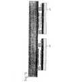
ここで考慮された、同じプレートに複数の装置を構成することが必要なケースでは、将来の装置にだけ脆いゾーンを形成することが有利である。そのため、構成部品に関して基板から分離され、装置間のスペース(脆いゾーンはない)によりプレートに保持されるゾーンを得ることを目的とする。図8(および図9)および図10では、第一および第二のプレートに参照符号25A、25Bとしてこれらの脆いゾーンを示した。 In the case considered here, where it is necessary to configure multiple devices on the same plate, it is advantageous to form a fragile zone only for future devices. Therefore, the aim is to obtain a zone that is separated from the substrate with respect to the components and is held on the plate by the space between the devices (no fragile zones). In FIG. 8 (and FIG. 9) and FIG. 10, these brittle zones are shown as
脆いゾーンを形成するには、たとえば水素イオンおよび/またはヘリウムイオン注入により、ガス種を導入する。水素イオンを選択する場合、3E16H+/cm2から1E17H+/cm2の範囲でドーズ量を選択可能である。将来の装置に関して脆いゾーンを特定化するには、たとえば、非注入ゾーンをマスクすることにより実施可能である。In order to form a fragile zone, gas species are introduced, for example, by hydrogen ion and / or helium ion implantation. When hydrogen ions are selected, the dose can be selected in the range of 3E16H+ / cm2 to 1E17H+ / cm2 . To identify a fragile zone for future devices, it can be done, for example, by masking a non-implanted zone.
補剛材をなす層24Aまたは24B、たとえば酸化物の層は、こうした注入後にのみ堆積可能である。この層により、ブリスターを形成せずに分離が得られる。その場合、層が自己支持されるという条件になる(FR−A−2738671参照)。 A
たとえば、厚さ数ミクロン、たとえば5ミクロンの酸化シリコン層を堆積可能であり、あるいは薄いガラス薄膜(たとえば30ミクロン)を堆積可能である。 For example, a silicon oxide layer that is several microns thick, for example 5 microns, can be deposited, or a thin glass film (for example, 30 microns) can be deposited.
このように準備されたプレートで、構成部品LCDに必要なアクティブマトリクスまたはカラーフィルタを得られる全てのステップを実施する。図9は、カラーフィルタ26Aの様々な素子を形成したプレート21Aを示し、図10は、アクティブマトリクスの様々な素子26B(TFTトランジスタ(「Thin Film Transistors」およびCA素子(アドレッシング回路))を形成したプレート21Bを示している。 With the plate prepared in this way, all steps are carried out to obtain the active matrix or color filter required for the component LCD. FIG. 9 shows a
次に、局部的な注入ゾーンで、基板または疑似基板から装置の一部を備えた薄膜を分離可能にする処理を行う。たとえば、この処理は、450℃の範囲にある温度による熱処理であり、局部的な分離または著しい脆化を得ることにより、機械的な力を用いて後で分離を可能にする。図11では、引き離しゾーンを実線で示し、図9、10の脆化ゾーンとは区別している。 Next, in the local injection zone, a process is performed that makes it possible to separate the thin film with a part of the device from the substrate or pseudo-substrate. For example, this treatment is a heat treatment at a temperature in the range of 450 ° C., allowing subsequent separation using mechanical force by obtaining local separation or significant embrittlement. In FIG. 11, the separation zone is indicated by a solid line, and is distinguished from the embrittlement zone of FIGS.
その後、この二つのプレートは、それらの構成部品と共に、従来の方法に従って接着ビードにより組み立てられる。このビードが引き離し条件に適合する場合、組み立て後、局部的な引き離しを実施可能である。 The two plates are then assembled together with their components by adhesive beads according to conventional methods. If this bead meets the pull-off conditions, a local pull-out can be performed after assembly.
図11では、スペーサ26Cと共に上下逆に組み立てられた2個のプレートが、各TFTトランジスタ群と各カラーフィルタとを同時に囲んでいることが分かる。 In FIG. 11, it can be seen that two plates assembled upside down with the
次に、LCDスクリーンを形成する従来のステップ、すなわち、液晶の充填および封入を実施する(図12参照)。 Next, the conventional steps of forming the LCD screen are performed, i.e. filling and enclosing the liquid crystal (see FIG. 12).
その後、図13、14から分かるように、従来のダイヤモンドカット技術(「scribe and break」)により所望の寸法に下方プレートをカットする。その場合、ガラス基板は、(上記引き離しにより)垂直に、また(上記カットにより)側面に、構成部品の他の部分から分離される。脆化ゾーンで完全な引き離しを得るには、機械応力を及ぼすことが必要な場合がある。 Thereafter, as can be seen in FIGS. 13 and 14, the lower plate is cut to the desired dimensions by conventional diamond cutting techniques (“scribe and break”). In that case, the glass substrate is separated from other parts of the component vertically (by the pulling-off) and side-by-side (by the cutting). It may be necessary to exert a mechanical stress in order to obtain complete detachment in the embrittlement zone.
有利には、最終基板への移転前に多結晶シリコン層の全部または一部を除去できる。そのため、図15に示した例では、この多結晶シリコンの残留部分全体を、ここではプラスチック基板40である最終基板に構成部品を貼り合わせる前に除去できる。有利には、プラスチック基板を偏光子とすることができる。対象とされる用途に応じて偏光子の厚みを選択可能である。 Advantageously, all or part of the polycrystalline silicon layer can be removed before transfer to the final substrate. Therefore, in the example shown in FIG. 15, the entire remaining portion of the polycrystalline silicon can be removed before the components are bonded to the final substrate, which is here the
その後、上方プレートでカット操作を繰り返し(図15)、最終的に、2個の偏光子40、41の間にLCDスクリーンを得(図16、17)、作成する役割をするガラスは存在しない。 Thereafter, the cutting operation is repeated on the upper plate (FIG. 15), and finally an LCD screen is obtained between the two
Claims (38)
Translated fromJapanese第一および第二の付加層(22A、22B)を第一および第二の基板(21A、21B)に形成し、各第一および第二の付加層の少なくとも一部は局部的に脆化可能であり、各基板と脆化される付加層の少なくとも一部とが、異なる材料からなり、および/または異なるミクロ構造を有する、準備ステップと、
付加層における脆化可能な各部分の所定の位置だけに、局部的に脆い副層(25A、25B)を生成する脆化ステップと、
前記付加層の局部的に脆い副層に面する位置に、複数の構成部品または前記構成部品の一部(26A、26B)を補完する部分を形成する加工ステップと、
構成部品を補完する部分が向かい合い、両方の付加層の局部的に脆い副層が構成部品または構成部品の一部を含む薄膜を画定するように、付加層とともに2個の基板を上下逆に組み立てる結合ステップと、
分離ステップとを含み、該分離ステップが、脆化ステップと結合ステップとの間で一部を実施可能であり、複数の構成部品または構成部品の一部の個別の引き離しが、前記局部的に脆い副層に沿って前記脆化可能な部分で引き起こされる、製造方法。At least one component or part of the componentsof (26A, 26B) a manufacturinghowto produce a thin film,
The first and second additional layers (22A, 22B) are formed on the first and second substrates (21A, 21B), and at least a part of each of the first and second additional layers can be locally embrittled. A preparatory step, wherein each substrateand at least part of the additional layer to be embrittled are made of different materials and / or have different microstructures;
An embrittlement step for generatinglocally fragile sublayers (25A, 25B)only atpredetermined positions of each of the portions that can be embrittled in theadditional layer ;
Aposition facing the locally fragile sublayer of the additional layer, and the processing stepsin which a plurality of components or the construction part of the components of(26A, 26B) forming a portion ofcomplement,
Component ofcomplement to portionshave facingcase, aslocally fragile sub-layers of both of the additional layer to define a thin film containing a portion of the component or components, the two substratestogether with additional layers above and below A coupling step to assemble in reverse,
And a separation step, the separation step is a feasible part between the coupling steps andembrittlement step,a portion of the plurality of components or components of distancing individual, thelocal brittle A manufacturing methodcaused by theembrittleable portion along the sublayer.
Applications Claiming Priority (2)
| Application Number | Priority Date | Filing Date | Title |
|---|---|---|---|
| FR0102890AFR2821697B1 (en) | 2001-03-02 | 2001-03-02 | METHOD OF MANUFACTURING THIN LAYERS ON A SPECIFIC CARRIER AND AN APPLICATION |
| PCT/FR2002/000754WO2002071475A1 (en) | 2001-03-02 | 2002-03-01 | Method for producing thin layers on a specific support and an application thereof |
Publications (3)
| Publication Number | Publication Date |
|---|---|
| JP2004532515A JP2004532515A (en) | 2004-10-21 |
| JP2004532515A5 JP2004532515A5 (en) | 2005-12-22 |
| JP4384410B2true JP4384410B2 (en) | 2009-12-16 |
Family
ID=8860683
Family Applications (1)
| Application Number | Title | Priority Date | Filing Date |
|---|---|---|---|
| JP2002570292AExpired - LifetimeJP4384410B2 (en) | 2001-03-02 | 2002-03-01 | Thin film manufacturing method on special substrate and its application |
Country Status (7)
| Country | Link |
|---|---|
| US (1) | US6939782B2 (en) |
| EP (1) | EP1364400B9 (en) |
| JP (1) | JP4384410B2 (en) |
| AT (1) | ATE468606T1 (en) |
| DE (1) | DE60236410D1 (en) |
| FR (1) | FR2821697B1 (en) |
| WO (1) | WO2002071475A1 (en) |
Families Citing this family (18)
| Publication number | Priority date | Publication date | Assignee | Title |
|---|---|---|---|---|
| FR2874455B1 (en)* | 2004-08-19 | 2008-02-08 | Soitec Silicon On Insulator | HEAT TREATMENT BEFORE BONDING TWO PLATES |
| FR2839385B1 (en)* | 2002-05-02 | 2004-07-23 | Soitec Silicon On Insulator | PROCESS FOR TAKING OFF MATERIAL LAYERS |
| US6759277B1 (en)* | 2003-02-27 | 2004-07-06 | Sharp Laboratories Of America, Inc. | Crystalline silicon die array and method for assembling crystalline silicon sheets onto substrates |
| US7309446B1 (en)* | 2004-02-25 | 2007-12-18 | Metadigm Llc | Methods of manufacturing diamond capsules |
| EP1571705A3 (en)* | 2004-03-01 | 2006-01-04 | S.O.I.Tec Silicon on Insulator Technologies | Process of making a semiconductor structure on a substrate |
| FR2866983B1 (en) | 2004-03-01 | 2006-05-26 | Soitec Silicon On Insulator | REALIZING AN ENTITY IN SEMICONDUCTOR MATERIAL ON SUBSTRATE |
| KR101152141B1 (en)* | 2005-06-08 | 2012-06-15 | 삼성전자주식회사 | Liquid crystal display and making method of liquid crystal display panel |
| WO2007019487A2 (en)* | 2005-08-05 | 2007-02-15 | Reveo, Inc. | Method and system for fabricating thin devices |
| FR2935537B1 (en) | 2008-08-28 | 2010-10-22 | Soitec Silicon On Insulator | MOLECULAR ADHESION INITIATION METHOD |
| US7927975B2 (en) | 2009-02-04 | 2011-04-19 | Micron Technology, Inc. | Semiconductor material manufacture |
| FR2943177B1 (en) | 2009-03-12 | 2011-05-06 | Soitec Silicon On Insulator | METHOD FOR MANUFACTURING A MULTILAYER STRUCTURE WITH CIRCUIT LAYER REPORT |
| FR2947380B1 (en) | 2009-06-26 | 2012-12-14 | Soitec Silicon Insulator Technologies | METHOD OF COLLAGE BY MOLECULAR ADHESION. |
| US9847243B2 (en) | 2009-08-27 | 2017-12-19 | Corning Incorporated | Debonding a glass substrate from carrier using ultrasonic wave |
| FR2977069B1 (en) | 2011-06-23 | 2014-02-07 | Soitec Silicon On Insulator | METHOD FOR MANUFACTURING A SEMICONDUCTOR STRUCTURE USING TEMPORARY COLLAGE |
| JP5480321B2 (en) | 2012-03-21 | 2014-04-23 | 株式会社東芝 | Magnetic memory and manufacturing method thereof |
| WO2014020387A1 (en) | 2012-07-31 | 2014-02-06 | Soitec | Methods of forming semiconductor structures including mems devices and integrated circuits on opposing sides of substrates, and related structures and devices |
| FR2995136B1 (en)* | 2012-09-04 | 2015-06-26 | Soitec Silicon On Insulator | PSEUDO-SUBSTRATE WITH IMPROVED EFFICIENCY OF USE OF MONOCRYSTALLINE MATERIAL |
| US9209142B1 (en)* | 2014-09-05 | 2015-12-08 | Skorpios Technologies, Inc. | Semiconductor bonding with compliant resin and utilizing hydrogen implantation for transfer-wafer removal |
Family Cites Families (16)
| Publication number | Priority date | Publication date | Assignee | Title |
|---|---|---|---|---|
| US5300788A (en)* | 1991-01-18 | 1994-04-05 | Kopin Corporation | Light emitting diode bars and arrays and method of making same |
| WO1993018428A2 (en)* | 1992-03-13 | 1993-09-16 | Kopin Corporation | Head-mounted display system |
| FR2715501B1 (en)* | 1994-01-26 | 1996-04-05 | Commissariat Energie Atomique | Method for depositing semiconductor wafers on a support. |
| JP3352340B2 (en)* | 1995-10-06 | 2002-12-03 | キヤノン株式会社 | Semiconductor substrate and method of manufacturing the same |
| FR2744285B1 (en)* | 1996-01-25 | 1998-03-06 | Commissariat Energie Atomique | METHOD FOR TRANSFERRING A THIN FILM FROM AN INITIAL SUBSTRATE TO A FINAL SUBSTRATE |
| FR2748851B1 (en)* | 1996-05-15 | 1998-08-07 | Commissariat Energie Atomique | PROCESS FOR PRODUCING A THIN FILM OF SEMICONDUCTOR MATERIAL |
| US6127199A (en)* | 1996-11-12 | 2000-10-03 | Seiko Epson Corporation | Manufacturing method of active matrix substrate, active matrix substrate and liquid crystal display device |
| US6534380B1 (en)* | 1997-07-18 | 2003-03-18 | Denso Corporation | Semiconductor substrate and method of manufacturing the same |
| JPH11233449A (en)* | 1998-02-13 | 1999-08-27 | Denso Corp | Manufacture of semiconductor substrate |
| JP3809733B2 (en)* | 1998-02-25 | 2006-08-16 | セイコーエプソン株式会社 | Thin film transistor peeling method |
| JP4085459B2 (en)* | 1998-03-02 | 2008-05-14 | セイコーエプソン株式会社 | Manufacturing method of three-dimensional device |
| US6271101B1 (en)* | 1998-07-29 | 2001-08-07 | Semiconductor Energy Laboratory Co., Ltd. | Process for production of SOI substrate and process for production of semiconductor device |
| JP2000077287A (en)* | 1998-08-26 | 2000-03-14 | Nissin Electric Co Ltd | Manufacture of crystal thin-film substrate |
| FR2795866B1 (en)* | 1999-06-30 | 2001-08-17 | Commissariat Energie Atomique | METHOD FOR PRODUCING A THIN MEMBRANE AND MEMBRANE STRUCTURE THUS OBTAINED |
| JP3804349B2 (en)* | 1999-08-06 | 2006-08-02 | セイコーエプソン株式会社 | Thin film device device manufacturing method, active matrix substrate manufacturing method, and electro-optical device |
| AU6905000A (en)* | 1999-08-10 | 2001-03-05 | Silicon Genesis Corporation | A cleaving process to fabricate multilayered substrates using low implantation doses |
- 2001
- 2001-03-02FRFR0102890Apatent/FR2821697B1/ennot_activeExpired - Fee Related
- 2002
- 2002-03-01EPEP02708436Apatent/EP1364400B9/ennot_activeExpired - Lifetime
- 2002-03-01WOPCT/FR2002/000754patent/WO2002071475A1/enactiveApplication Filing
- 2002-03-01DEDE60236410Tpatent/DE60236410D1/ennot_activeExpired - Lifetime
- 2002-03-01JPJP2002570292Apatent/JP4384410B2/ennot_activeExpired - Lifetime
- 2002-03-01USUS10/469,633patent/US6939782B2/ennot_activeExpired - Lifetime
- 2002-03-01ATAT02708436Tpatent/ATE468606T1/ennot_activeIP Right Cessation
Also Published As
| Publication number | Publication date |
|---|---|
| JP2004532515A (en) | 2004-10-21 |
| US6939782B2 (en) | 2005-09-06 |
| WO2002071475A1 (en) | 2002-09-12 |
| FR2821697B1 (en) | 2004-06-25 |
| EP1364400A1 (en) | 2003-11-26 |
| EP1364400B9 (en) | 2012-03-21 |
| US20040110320A1 (en) | 2004-06-10 |
| EP1364400B1 (en) | 2010-05-19 |
| DE60236410D1 (en) | 2010-07-01 |
| FR2821697A1 (en) | 2002-09-06 |
| ATE468606T1 (en) | 2010-06-15 |
Similar Documents
| Publication | Publication Date | Title |
|---|---|---|
| JP4384410B2 (en) | Thin film manufacturing method on special substrate and its application | |
| US7045441B2 (en) | Method for forming a single-crystal silicon layer on a transparent substrate | |
| EP0924769B1 (en) | Method of transferring thin film devices | |
| KR100500520B1 (en) | A transferring method and a method for manufacturing an active matrix substrate | |
| TWI362547B (en) | Peeling method and method for manufacturing display device using the peeling method | |
| US6858517B2 (en) | Methods of producing a heterogeneous semiconductor structure | |
| US20030077885A1 (en) | Embrittled substrate and method for making same | |
| CN100592467C (en) | transfer method | |
| TW200403858A (en) | Method of transferring a laminate and method of manufacturing a semiconductor device | |
| JP2012160754A (en) | Process for cutting out block of material and process for forming thin film | |
| JP2004532515A5 (en) | ||
| JP2010118638A (en) | Manufacturing method of thin-film element | |
| KR101033551B1 (en) | Liquid crystal display substrate transfer jig and manufacturing method of liquid crystal display device using same | |
| JP4186502B2 (en) | Thin film device manufacturing method, thin film device, and display device | |
| JP2003068995A (en) | Method for manufacturing thin film device substrate | |
| JP2008203851A (en) | Gray scale mask manufacturing method using wafer bonding process | |
| JP2679676B2 (en) | SOI substrate manufacturing method and semiconductor device manufacturing method | |
| JP2002270617A (en) | Semiconductor device | |
| US6853414B2 (en) | Flat liquid crystal, screen operating in reflective mode and method for manufacturing this screen | |
| JP2003298029A (en) | Peeling transfer device, peeling transfer method, semiconductor device and IC card | |
| JP4748351B2 (en) | Thin film element manufacturing method | |
| JP2006310399A (en) | Thin film element manufacturing method and electronic device | |
| JP3278062B2 (en) | Semiconductor device and manufacturing method thereof | |
| JP5196212B2 (en) | Thin film device manufacturing method | |
| CN100481328C (en) | Flexible single crystal film and method for manufacturing the same |
Legal Events
| Date | Code | Title | Description |
|---|---|---|---|
| A521 | Request for written amendment filed | Free format text:JAPANESE INTERMEDIATE CODE: A523 Effective date:20050119 | |
| A621 | Written request for application examination | Free format text:JAPANESE INTERMEDIATE CODE: A621 Effective date:20050119 | |
| A131 | Notification of reasons for refusal | Free format text:JAPANESE INTERMEDIATE CODE: A131 Effective date:20080902 | |
| A601 | Written request for extension of time | Free format text:JAPANESE INTERMEDIATE CODE: A601 Effective date:20081126 | |
| A602 | Written permission of extension of time | Free format text:JAPANESE INTERMEDIATE CODE: A602 Effective date:20081203 | |
| A521 | Request for written amendment filed | Free format text:JAPANESE INTERMEDIATE CODE: A523 Effective date:20090217 | |
| TRDD | Decision of grant or rejection written | ||
| A01 | Written decision to grant a patent or to grant a registration (utility model) | Free format text:JAPANESE INTERMEDIATE CODE: A01 Effective date:20090901 | |
| A01 | Written decision to grant a patent or to grant a registration (utility model) | Free format text:JAPANESE INTERMEDIATE CODE: A01 | |
| A61 | First payment of annual fees (during grant procedure) | Free format text:JAPANESE INTERMEDIATE CODE: A61 Effective date:20090925 | |
| FPAY | Renewal fee payment (event date is renewal date of database) | Free format text:PAYMENT UNTIL: 20121002 Year of fee payment:3 | |
| R150 | Certificate of patent or registration of utility model | Ref document number:4384410 Country of ref document:JP Free format text:JAPANESE INTERMEDIATE CODE: R150 Free format text:JAPANESE INTERMEDIATE CODE: R150 | |
| FPAY | Renewal fee payment (event date is renewal date of database) | Free format text:PAYMENT UNTIL: 20131002 Year of fee payment:4 | |
| R250 | Receipt of annual fees | Free format text:JAPANESE INTERMEDIATE CODE: R250 | |
| R250 | Receipt of annual fees | Free format text:JAPANESE INTERMEDIATE CODE: R250 | |
| R250 | Receipt of annual fees | Free format text:JAPANESE INTERMEDIATE CODE: R250 | |
| R250 | Receipt of annual fees | Free format text:JAPANESE INTERMEDIATE CODE: R250 | |
| R250 | Receipt of annual fees | Free format text:JAPANESE INTERMEDIATE CODE: R250 | |
| R250 | Receipt of annual fees | Free format text:JAPANESE INTERMEDIATE CODE: R250 | |
| R250 | Receipt of annual fees | Free format text:JAPANESE INTERMEDIATE CODE: R250 | |
| R250 | Receipt of annual fees | Free format text:JAPANESE INTERMEDIATE CODE: R250 | |
| R250 | Receipt of annual fees | Free format text:JAPANESE INTERMEDIATE CODE: R250 | |
| R250 | Receipt of annual fees | Free format text:JAPANESE INTERMEDIATE CODE: R250 | |
| EXPY | Cancellation because of completion of term |