JP4382593B2 - Probe unit and manufacturing method thereof - Google Patents
Probe unit and manufacturing method thereofDownload PDFInfo
- Publication number
- JP4382593B2 JP4382593B2JP2004190963AJP2004190963AJP4382593B2JP 4382593 B2JP4382593 B2JP 4382593B2JP 2004190963 AJP2004190963 AJP 2004190963AJP 2004190963 AJP2004190963 AJP 2004190963AJP 4382593 B2JP4382593 B2JP 4382593B2
- Authority
- JP
- Japan
- Prior art keywords
- layer
- manufacturing
- substrate
- probe unit
- probe
- Prior art date
- Legal status (The legal status is an assumption and is not a legal conclusion. Google has not performed a legal analysis and makes no representation as to the accuracy of the status listed.)
- Expired - Fee Related
Links
- 239000000523sampleSubstances0.000titleclaimsdescription198
- 238000004519manufacturing processMethods0.000titleclaimsdescription123
- 239000010410layerSubstances0.000claimsdescription440
- 239000000758substrateSubstances0.000claimsdescription98
- 239000002344surface layerSubstances0.000claimsdescription65
- 239000000463materialSubstances0.000claimsdescription51
- 238000000034methodMethods0.000claimsdescription20
- 239000004020conductorSubstances0.000claimsdescription13
- WABPQHHGFIMREM-UHFFFAOYSA-Nlead(0)Chemical compound[Pb]WABPQHHGFIMREM-UHFFFAOYSA-N0.000claimsdescription4
- 238000010586diagramMethods0.000description31
- 229910001030Iron–nickel alloyInorganic materials0.000description14
- 238000007747platingMethods0.000description14
- 230000001681protective effectEffects0.000description8
- 229910000990Ni alloyInorganic materials0.000description7
- 229910003266NiCoInorganic materials0.000description7
- 229910003289NiMnInorganic materials0.000description7
- 239000002184metalSubstances0.000description6
- 229910052751metalInorganic materials0.000description6
- 229910052782aluminiumInorganic materials0.000description4
- 230000015572biosynthetic processEffects0.000description4
- 229910052737goldInorganic materials0.000description4
- 229910052759nickelInorganic materials0.000description4
- 238000003801millingMethods0.000description3
- 238000005498polishingMethods0.000description3
- 229910001020Au alloyInorganic materials0.000description2
- SECXISVLQFMRJM-UHFFFAOYSA-NN-MethylpyrrolidoneChemical compoundCN1CCCC1=OSECXISVLQFMRJM-UHFFFAOYSA-N0.000description2
- 239000000853adhesiveSubstances0.000description2
- 230000001070adhesive effectEffects0.000description2
- 239000000919ceramicSubstances0.000description2
- 238000005520cutting processMethods0.000description2
- 230000002500effect on skinEffects0.000description2
- 239000011521glassSubstances0.000description2
- 239000002241glass-ceramicSubstances0.000description2
- 238000007689inspectionMethods0.000description2
- 229910052741iridiumInorganic materials0.000description2
- 229910052763palladiumInorganic materials0.000description2
- 229920001296polysiloxanePolymers0.000description2
- 239000011347resinSubstances0.000description2
- 229920005989resinPolymers0.000description2
- 229910052703rhodiumInorganic materials0.000description2
- 229910052710siliconInorganic materials0.000description2
- 239000010703siliconSubstances0.000description2
- 238000004544sputter depositionMethods0.000description2
- 239000000126substanceSubstances0.000description2
- 238000001039wet etchingMethods0.000description2
- 238000005452bendingMethods0.000description1
- 239000003795chemical substances by applicationSubstances0.000description1
- 238000009713electroplatingMethods0.000description1
- 238000005530etchingMethods0.000description1
- 238000005304joiningMethods0.000description1
- 239000007788liquidSubstances0.000description1
- 239000004973liquid crystal related substanceSubstances0.000description1
- 230000000873masking effectEffects0.000description1
- 229920002120photoresistant polymerPolymers0.000description1
- 238000007493shaping processMethods0.000description1
Images


Classifications
- G—PHYSICS
- G01—MEASURING; TESTING
- G01R—MEASURING ELECTRIC VARIABLES; MEASURING MAGNETIC VARIABLES
- G01R1/00—Details of instruments or arrangements of the types included in groups G01R5/00 - G01R13/00 and G01R31/00
- G01R1/02—General constructional details
- G01R1/06—Measuring leads; Measuring probes
- G01R1/067—Measuring probes
- G01R1/073—Multiple probes
- G—PHYSICS
- G01—MEASURING; TESTING
- G01R—MEASURING ELECTRIC VARIABLES; MEASURING MAGNETIC VARIABLES
- G01R3/00—Apparatus or processes specially adapted for the manufacture or maintenance of measuring instruments, e.g. of probe tips
- G—PHYSICS
- G01—MEASURING; TESTING
- G01R—MEASURING ELECTRIC VARIABLES; MEASURING MAGNETIC VARIABLES
- G01R1/00—Details of instruments or arrangements of the types included in groups G01R5/00 - G01R13/00 and G01R31/00
- G01R1/02—General constructional details
- G01R1/06—Measuring leads; Measuring probes
- G01R1/067—Measuring probes
- G01R1/073—Multiple probes
- G01R1/07307—Multiple probes with individual probe elements, e.g. needles, cantilever beams or bump contacts, fixed in relation to each other, e.g. bed of nails fixture or probe card
- G01R1/07342—Multiple probes with individual probe elements, e.g. needles, cantilever beams or bump contacts, fixed in relation to each other, e.g. bed of nails fixture or probe card the body of the probe being at an angle other than perpendicular to test object, e.g. probe card
- H—ELECTRICITY
- H01—ELECTRIC ELEMENTS
- H01L—SEMICONDUCTOR DEVICES NOT COVERED BY CLASS H10
- H01L22/00—Testing or measuring during manufacture or treatment; Reliability measurements, i.e. testing of parts without further processing to modify the parts as such; Structural arrangements therefor
- Y—GENERAL TAGGING OF NEW TECHNOLOGICAL DEVELOPMENTS; GENERAL TAGGING OF CROSS-SECTIONAL TECHNOLOGIES SPANNING OVER SEVERAL SECTIONS OF THE IPC; TECHNICAL SUBJECTS COVERED BY FORMER USPC CROSS-REFERENCE ART COLLECTIONS [XRACs] AND DIGESTS
- Y10—TECHNICAL SUBJECTS COVERED BY FORMER USPC
- Y10T—TECHNICAL SUBJECTS COVERED BY FORMER US CLASSIFICATION
- Y10T29/00—Metal working
- Y10T29/49—Method of mechanical manufacture
- Y10T29/49002—Electrical device making
- Y10T29/49117—Conductor or circuit manufacturing
- Y10T29/49124—On flat or curved insulated base, e.g., printed circuit, etc.
- Y10T29/49155—Manufacturing circuit on or in base
- Y10T29/49156—Manufacturing circuit on or in base with selective destruction of conductive paths
Landscapes
- Physics & Mathematics (AREA)
- General Physics & Mathematics (AREA)
- Engineering & Computer Science (AREA)
- Manufacturing & Machinery (AREA)
- Computer Hardware Design (AREA)
- Microelectronics & Electronic Packaging (AREA)
- Power Engineering (AREA)
- Measuring Leads Or Probes (AREA)
- Testing Or Measuring Of Semiconductors Or The Like (AREA)
Description
Translated fromJapanese本発明はプローブユニット及びその製造方法に関する。 The present invention relates to a probe unit and a manufacturing method thereof.
従来、並列配置された複数の導線が基板から突出し、その先端部分が検体の電極と接触するプローブユニットが知られている。特許文献1に記載されたプローブユニットでは導線が基板から突出しているため、オーバードライブをかけると導線の先端部およびその近傍が撓む。そのため導線の先端部と検体の電極とを適切な接触圧で確実に導通させることができる。
従来のプローブユニットでは、特許文献1などに開示されているとおり、導線の厚さが均一である。また導線を形成する材料および導線の厚さは、導線の基板から突出する部分の耐久性および上述の接触圧を考慮して設計される。そのため特許文献1に記載されたプローブユニットでは、導線を電気抵抗率の低い材料で形成したり導線を厚くしたりすることにより、導線の電気抵抗を小さく設計することは容易ではない。また導線の幅は検体の電極のピッチに応じて設計される。そのため導線の幅を広くすることにより、導線の電気抵抗を小さくすることができない。このようなプローブユニットでは、導体損が大きくなるため導通試験で使用可能な信号の周波数が狭くなる等の問題がある。2. Description of the Related Art Conventionally, a probe unit is known in which a plurality of conductors arranged in parallel protrude from a substrate and the tip portion thereof contacts an electrode of a specimen. In the probe unit described in Patent Document 1, since the conducting wire protrudes from the substrate, the tip of the conducting wire and its vicinity are bent when overdrive is applied. Therefore, it is possible to reliably conduct the leading end portion of the conducting wire and the electrode of the specimen with an appropriate contact pressure.
In the conventional probe unit, as disclosed in Patent Document 1 and the like, the thickness of the conducting wire is uniform. The material for forming the conductive wire and the thickness of the conductive wire are designed in consideration of the durability of the portion protruding from the substrate of the conductive wire and the contact pressure described above. Therefore, in the probe unit described in Patent Document 1, it is not easy to design the electrical resistance of the conducting wire to be small by forming the conducting wire with a material having a low electrical resistivity or by increasing the thickness of the conducting wire. The width of the conducting wire is designed according to the pitch of the electrode of the specimen. Therefore, the electrical resistance of the conducting wire cannot be reduced by increasing the width of the conducting wire. In such a probe unit, there is a problem that the frequency of a signal that can be used in a continuity test becomes narrow because the conductor loss increases.
一方、特許文献2には、複数の導線がフィルム上に形成され、導線の先端部分がフィルムから突出し、先端部分より後端側に設けられている中間部分が先端部分と異なる材料で形成されるプローブユニットが開示されている。特許文献2に記載のプローブユニットでは、導線の中間部分を先端部分よりも電気抵抗率の低い材料で形成することができる。つまり、導線の電気抵抗を小さくできるため、導体損を小さくでき、導通試験で使用可能な信号の周波数を拡げることができる。
しかしながら、特許文献2に記載のプローブユニットは、支持金属板上に導線を形成し、導線のフィルムから突出させない部分とフィルムとを接着剤で接合し、支持金属板を分離して製造される。導線を支持金属板上に形成するため、導線の支持金属板側は平坦になる。また導線とフィルムとを接着剤で接合するため、導線のフィルム側には大きな段差を設けることができない。つまり特許文献2に記載のプローブユニットでは、導線の厚さを自由に設計して導線の電気抵抗を小さくすることができない。
However, the probe unit described in
本発明は、上記の問題に鑑みてなされたものであって、適切な接触圧で検体と確実に導通させることができ、導線の電気抵抗を小さくできるプローブユニット、及びその製造方法を提供することを目的とする。 The present invention has been made in view of the above problems, and provides a probe unit that can be reliably connected to a specimen with an appropriate contact pressure and can reduce the electrical resistance of a conducting wire, and a method for manufacturing the probe unit. With the goal.
上記目的を達成するためのプローブユニットの製造方法は、基板と、前記基板上に形成され、前記基板の縁部から突出し検体の電極に接触する先端部、前記先端部よりも厚い厚肉部、前記先端部と前記厚肉部との間に位置し前記先端部と同一厚さの薄肉部、前記先端部と前記薄肉部と前記厚肉部の下部層とに相当する第一層、および、前記厚肉部の上部層に相当し前記第一層と異なる材質の第二層を有する導線と、を備えるプローブユニットの製造方法であって、前記基板に凹部を形成する凹部形成工程と、前記基板上に前記凹部を埋める犠牲層を形成する犠牲層形成工程と、一端が前記犠牲層上に位置する前記第一層を前記犠牲層および前記基板上に形成する第一層形成工程と、少なくとも前記一端を除く前記第一層上に前記第二層を形成する第二層形成工程と、前記犠牲層を除去する犠牲層除去工程と、を含む。一端が犠牲層上に位置する第一層を犠牲層および基板上に形成し、犠牲層を除去するため、第一層の一端は基板の凹部に突出する。また少なくとも一端を除く第一層上に第二層を形成するため、第二層が第一層に形成されている部分は第二層が第一層に形成されていない部分と比較して第二層の厚さだけ厚くなる。つまり請求項1に係るプローブユニットの製造方法によれば、導線の先端部に相当する第一層の一端が基板から突出するプローブユニットを製造できる。
尚、本明細書において、「・・・上に形成する」とは、技術上の阻害要因がない限りにおいて、「・・・上に直に形成する」と、「・・・上に中間物を介して形成する」の両方を含む意味とする。
請求項1に記載の製造方法により製造されるプローブユニットは、基板と、前記基板上に形成され、前記基板の縁部から突出し検体の電極に接触する先端部と前記先端部よりも厚い厚肉部とを有する導線と、を備える。導線の先端部が基板の縁部から突出するので、オーバードライブをかけると先端部およびその近傍が撓む。そのため検体の電極に導線の先端部を適切な接触圧で確実に導通できる。ここで導線の先端部およびその近傍の厚さは、その耐久性と上述の接触圧とを考慮して設計されることが望ましい。そのため導線の先端部およびその近傍を厚くすることにより、導線の電気抵抗を小さくすることはできない。しかしながら導線は先端部と比較して厚い厚肉部を有している。そのため厚肉部の厚さを導線の電気抵抗を考慮して設計すれば、導線の電気抵抗を小さくすることができる。
前記導線は、前記先端部と前記厚肉部との間に前記先端部と同一厚さの薄肉部を有する。
また、前記導線は、前記先端部と前記薄肉部と前記厚肉部の下部層とに相当する第一層と、前記厚肉部の上部層に相当し前記第一層と異なる材質の第二層とを有する。第一層は先端部および薄肉部に相当する。そのため第一層を形成する材料は、オーバードライブによる先端部と検体の電極との接触圧と、その耐久性とを考慮して設計されるのが望ましい。上述の接触圧と耐久性とを考慮して第一層を設計すると、第一層を電気抵抗率の低い材料で形成するなどして、導線の電気抵抗を小さくすることは容易ではない。しかしながら導線は、第一層と異なる材質の第二層を有する。そのため第二層を第一層と比較して電気抵抗率の低い材料で形成すれば、導線の電気抵抗を小さくすることができる。
前記厚肉部と前記薄肉部との境界は、前記導線の前記基板上に形成されている部位に位置してもよい。A probe unit manufacturing method for achieving the above object includes a substrate, a tip formed on the substrate, protruding from an edge of the substrate and contacting an electrode of a specimen, a thick portion thicker than the tip, A thin layer located between the tip portion and the thick portion and having the same thickness as the tip portion, a first layer corresponding to the tip portion, the thin portion, and a lower layer of the thick portion; and A conductor unit having a second layer made of a material different from the first layer and corresponding to the upper layer of the thick-walled portion, and a recess forming step of forming a recess in the substrate; A sacrificial layer forming step of forming a sacrificial layer filling the concave portion on the substrate, a first layer forming step of forming the first layer having one end positioned on the sacrificial layer on the sacrificial layer and the substrate, at least Forming the second layer on the first layer excluding the one end That includes a second layer forming step, a sacrificial layer removing step of removing the sacrificial layer. In order to form a first layer having one end positioned on the sacrificial layer on the sacrificial layer and the substrate and remove the sacrificial layer, one end of the first layer protrudes into the recess of the substrate. Since the second layer is formed on the first layer except at least one end, the portion where the second layer is formed on the first layer is compared with the portion where the second layer is not formed on the first layer. Thicken by two layers. That is, according to the probe unit manufacturing method of the first aspect, it is possible to manufacture a probe unit in which one end of the first layer corresponding to the leading end portion of the conducting wire protrudes from the substrate.
In the present specification, “... formed on” means “... formed directly on” and “... on the intermediate” unless there is a technical impediment. It is meant to include both “formed through”.
A probe unitmanufactured by the manufacturing method according to claim 1 is a substrate, a tip formed on the substrate, protruding from an edge of the substrate and contacting a specimen electrode, and thicker than the tip A conductor having a portion. Since the leading end portion of the conducting wire protrudes from the edge portion of the substrate, when the overdrive is applied, the leading end portion and the vicinity thereof are bent. Therefore, it is possible to reliably conduct the tip of the lead wire to the electrode of the specimen with an appropriate contact pressure. Here, it is desirable that the thickness of the leading end portion and the vicinity thereof be designed in consideration of the durability and the contact pressure described above. For this reason, the electrical resistance of the conducting wire cannot be reduced by increasing the thickness of the leading end of the conducting wire and the vicinity thereof. However, the conducting wire has a thick part thicker than the tip part. Therefore, if the thickness of the thick portion is designed in consideration of the electrical resistance of the conducting wire, the electrical resistance of the conducting wire can be reduced.
The conductorwill have the said front end portion and the thin portion of the same thickness between the thick portion and the distal portion.
The conducting wire includes a first layer corresponding to the tip portion, the thin portion, and a lower layer of the thick portion, and a second material made of a material different from the first layer corresponding to the upper layer of the thick portion. And having a layer. The first layer corresponds to the tip portion and the thin portion. Therefore, it is desirable that the material forming the first layer is designed in consideration of the contact pressure between the tip portion and the electrode of the specimen due to overdrive and its durability. When the first layer is designed in consideration of the contact pressure and durability described above, it is not easy to reduce the electrical resistance of the conducting wire by forming the first layer with a material having a low electrical resistivity. However, the conducting wire has a second layer of a material different from the first layer. Therefore, if the second layer is formed of a material having a lower electrical resistivity than the first layer, the electrical resistance of the conducting wire can be reduced.
The boundary between the thick part and the thin part may be located at a portion of the conducting wire formed on the substrate.
前記厚肉部と前記薄肉部との境界は、前記導線の前記基板の前記縁部から突出する部位に位置するのが望ましい。オーバードライブによって先端部およびその近傍が撓むと導線が基板から剥離する方向の力が導線に加わる。特に基板の縁部近傍の導線が撓むとその力が大きくなる。しかしながら厚肉部と薄肉部との境界が導線の基板の縁部から突出する部位に位置するため、基板の縁部近傍における導線の撓みを小さくできる。そのため導線が基板の縁部から剥離することを防止できる。
前記導線の前記基板と反対側の表面に、前記厚肉部と前記薄肉部との境界の段差が形成されていてもよい。It is desirable that the boundary between the thick part and the thin part is located at a portion protruding from the edge of the substrate of the conductor. When the tip portion and its vicinity are bent by overdrive, a force in a direction in which the conductive wire is peeled off from the substrate is applied to the conductive wire. In particular, when the conducting wire near the edge of the substrate is bent, the force increases. However, since the boundary between the thick portion and the thin portion is located at a portion protruding from the edge of the conductor substrate, the deflection of the conductor near the edge of the substrate can be reduced. Therefore, it can prevent that a conducting wire peels from the edge part of a board | substrate.
A step at the boundary between the thick part and the thin part may be formed on the surface of the conducting wire opposite to the substrate.
前記導線は、内部と異なる材質の表面層を有するのが望ましい。表面層を電気抵抗率の低い材料で形成すれば、導線の電気抵抗を小さくできる。特に高周波の電気信号は表皮効果によって表面層を伝わるので、高周波の電気信号に対する導体損を効果的に低減できる。また導線の先端部の表面に先端部の内部よりも硬質な材料で表面層を形成すれば、導線の先端部が検体の電極との接触によって摩耗することを抑制できる。 It is desirable that the conducting wire has a surface layer made of a material different from the inside. If the surface layer is formed of a material having a low electrical resistivity, the electrical resistance of the conducting wire can be reduced. In particular, since a high frequency electrical signal is transmitted through the surface layer by the skin effect, the conductor loss for the high frequency electrical signal can be effectively reduced. Further, if the surface layer is formed of a material harder than the inside of the tip portion on the surface of the tip portion of the lead wire, it is possible to suppress the tip portion of the lead wire from being worn by contact with the electrode of the specimen.
以下、本発明の実施の形態を図面に基づいて説明する。まずプローブユニットの構成を複数の実施例に基づいて説明する。
(プローブユニットの第一実施例)
図1は本発明のプローブユニットの第一実施例によるプローブユニット1の構成を表す模式図である。プローブユニット1は、プローブ4と液晶パネルやIC(Integrated Circuit)等の検体5の電極5aとを導通させて検体5の電気的特性を検査するために用いるものである(図7参照)。プローブユニット1は、後述するオーバードライブによる検体5の電極5aとの接触圧を考慮して設計可能な薄肉部4bと、プローブ4の電気抵抗を考慮して設計可能な厚肉部4cとを有する。そのため適切な接触圧で検体5の電極5aと接触させて導通させることができるとともに、プローブ4の電気抵抗を小さくできる。Hereinafter, embodiments of the present invention will be described with reference to the drawings. First, the configuration of the probe unit will be described based on a plurality of embodiments.
(First embodiment of the probe unit)
FIG. 1 is a schematic diagram showing the configuration of a probe unit 1 according to a first embodiment of the probe unit of the present invention. The probe unit 1 is used to inspect the electrical characteristics of the
基板2はセラミックで板状に形成されている。尚、基板2はガラスセラミック、ガラス、シリコン、金属等の無機物の他、樹脂でもよい。
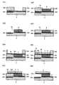
基板2上には複数のプローブ4が形成されている。導線としてのプローブ4は、先端部4a、薄肉部4b、および厚肉部4cを有する。先端部4aは基板2の縁部2aから突出している。薄肉部4bは先端部4aと厚肉部4cとの間に形成されている。薄肉部4bは先端部4aと同じ厚さに形成され、厚肉部4cは先端部4aおよび薄肉部4bと比較して厚く形成されている。本実施例では、薄肉部4bと厚肉部4cとの境界40が基板2上に位置し、薄肉部4bと厚肉部4cとによる段差42がプローブ4の表面の基板2と反対側に形成されているプローブユニット1について説明するが、プローブユニットの形状はこれに限定されない。例えばプローブユニットの第二実施例で説明するプローブユニット161のプローブ4のように、薄肉部4bと厚肉部4cとの境界40が基板2上に位置していなくてもよいし(図9参照)、図2に示すプローブユニット111のプローブ4のように、段差42がプローブ4の表面の基板2側に形成されていてもよい。The
A plurality of
プローブ4は、第一層6と第二層8と表面層10とを有している。
先端部4a、薄肉部4bおよび厚肉部4cの下部層としての第一層6は、基板2上に形成されている。先端部4aとしての第一層6の一端6aは、基板2の縁部2aから突出している。第一層6の基板2の縁部2aから突出する部分は、後述するオーバードライブによりプローブ4の先端部4aが検体5の電極5aに接触した状態で撓む(図7参照)。そのため第一層6の材料とその厚さとは、オーバードライブによる先端部4aと検体5の電極5aとの接触圧と、その耐久性とを考慮して設計されるのが望ましい。
表1は、図3のようにNiFeで形成した第一層6でオーバードライブの距離(OD)に対する接触圧(W)および応力(σ)の関係を検証した実験結果である。第一層6は、幅(B)50μm、基板2の縁部2aから突出する部分の長さ(L)1.2mmのものを用いた。NiFeのヤング率(E)は21414kgf/mm2であり、降伏点は130kgf/mm2であるとする。The
A
Table 1 shows the experimental results of verifying the relationship between the contact pressure (W) and the stress (σ) with respect to the overdrive distance (OD) in the

この実験結果によると、厚さ(T)0.02mmの第一層6では、オーバードライブ距離(OD)が0.05mmから0.2mmまでの範囲で降伏点より小さい応力(σ)になる。例えば、オーバードライブ距離(OD)が0.2mmのときの応力(σ)は89.225kgf/mm2であり、降伏点の130kgf/mm2よりも小さい。一方、厚さ(T)0.03mmの第一層6では、オーバードライブ距離(OD)が0.2mmで降伏点より大きな応力(σ:133.838kgf/mm2)となる。つまりオーバードライブの距離が0.05mmから0.2mmで使用されるプローブユニット1の第一層6は、NiFeで、厚さ0.02mm、幅50μm、基板2の縁部2aから突出する部分の長さ1.2mmに形成すればよい。尚、第一層6を形成する材料は、NiFeに限定されない。例えば第一層6を形成する材料は、NiCo、NiMn等のNi合金でもよいし、Niでもよい。According to this experimental result, in the
第二層8は第一層6上に形成されている。厚肉部4cの上部層としての第二層8は、オーバードライブにより撓まない。そのため第二層8の材料とその厚さとは、プローブ4の電気抵抗を考慮して設計されることが望ましい。例えば第二層8はCuで形成する。尚、第二層8は第一層6の材料よりも電気抵抗率の低い材料で形成されることが望ましいが、Cuに限定されない。例えば第二層8の材料は、第一層6と同一材料のNiFeでもよいし、NiCo、NiMn等のNi合金でもよいし、Ni、Au、Al等でもよい。 The
表面層10は、第一層6上と第二層8上とにAuで形成されている。尚、表面層10は、電気抵抗率の低い材料で形成されることが望ましいが、Auに限定されない。例えば表面層10の材料は、Au合金、Pd、Rh、Ir等でもよい。また表面層10の形状およびその配置は、図1に示す形状および配置に限定されない。例えば図4に示すプローブユニット121のように、第一層6および第二層8の表面を覆う表面層10を形成してもよい。また図5に示すプローブユニット131のように、第一層6上と第二層8上とにそれぞれ表面層10としての第一表面層10aと第二表面層10bとを形成してもよいし、第一層6上と第二層8上とのいずれか一方に表面層10を形成してもよい。また検体5の検査の仕様を満足するのであれば、図6に示すプローブユニット141のように表面層を有していなくてもよい。 The
表2は、第一層6の厚さ(T1)、第二層8の厚さ(T2)、および表面層10の厚さ(T3)とプローブの電気抵抗(R)との関係の算出結果である。プローブは、幅50μm、基板2の縁部2aから突出する部分(突出部)の長さ1.2mm、基板2上に形成されている部分(配線部)の長さ3.0mmとしている。NiFeで形成されている第一層6の電気抵抗(R1)、Cuで形成されている第二層8の電気抵抗(R2)、およびAuで形成されている表面層10の電気抵抗(R3)は、それぞれNiFeの電気抵抗率を20μΩcm、Cuの電気抵抗率を2μΩcm、Auの電気抵抗率を3μΩcmとして算出している。尚、プローブが有していない層は、その層の厚さを0で示している。 Table 2 shows the calculation results of the relationship between the thickness (T1) of the
この算出結果によると、第二層8および表面層10を有しているプローブ4(プローブC)では、第二層および表面層を有していないプローブ(プローブA)と比較して、0.693Ωの電気抵抗を低減できる。また第二層8を有しているが表面層を有していないプローブ4(プローブB)では、プローブAと比較して0.571Ωの電気抵抗を低減できる。 According to this calculation result, the probe 4 (probe C) having the
図7は、プローブユニット1を用いた検体5の電気的特性の検査方法を説明する模式図である。プローブ4の先端部4aと検体5の電極5aとを一対一で接触させて、プローブ4と検体5の電極5aとを導通させる。
まず図7(A1)、(B1)に示すように、プローブ4と検体5の電極5aが一対一で対応するように、プローブユニット1を検体5に対して配置する。FIG. 7 is a schematic diagram for explaining an inspection method for the electrical characteristics of the
First, as shown in FIGS. 7A1 and 7B1, the probe unit 1 is arranged with respect to the
次に図7(A2)、(B2)に示すように、プローブユニット1を検体5に接近させてプローブ4の先端部4aを電極5aに接触させる。さらにプローブユニット1を検体5に接近させると(すなわち、オーバードライブをかけると)、プローブ4の先端部4aと薄肉部4bの一部とはオーバードライブにより撓む。このとき第一層6の材料とその厚さとがオーバードライブによる接触圧を考慮して設計されていれば、プローブ4の先端部4aと検体5の電極5aとを適切な接触圧で接触させることができる。 Next, as shown in FIGS. 7A2 and 7B2, the probe unit 1 is brought close to the
次に、プローブ4と検体5の電極5aとを導通させた状態で、検査装置本体からプローブ4を通じて電極5aに検査信号を入力し、検体5の電気的特性を検査する。このときプローブ4の電気抵抗が小さければ、広範囲の周波数の検査信号を使用して検体5の検査を行うことができる。
検査終了後に検体5とプローブユニット1を離間させると、プローブ4は弾性により検査前の状態に復元する。Next, in a state where the
When the
以上説明したプローブユニットの第一実施例に係るプローブユニット1によると、プローブ4の先端部4aと薄肉部4bの一部とが基板2の縁部2aから突出するため、オーバードライブをかけるとプローブ4の先端部4aが検体5の電極5aに接触した状態でプローブ4の先端部4aと薄肉部4bの一部とが撓む。そのため第一層6の材料とその厚さとをオーバードライブによる接触圧を考慮して設計すれば、検体5の電極5aにプローブ4の先端部4aを適切な接触圧で接触させてプローブ4と電極5aとを確実に導通させることができる。 According to the probe unit 1 according to the first embodiment of the probe unit described above, the
しかしながら、第一層6の材料とその厚さとをオーバードライブによる接触圧を考慮して設計すると、プローブ4の電気抵抗を小さく設計することは容易ではない。しかしながら、プローブユニット1の厚肉部4cは第二層8を有している。そのため第二層8の厚さだけ厚肉部4cの厚さが厚くなる。さらに第二層8の材料とその厚さとをプローブ4の電気抵抗を考慮して設計することもできるため、プローブ4の電気抵抗を小さくできる。つまりプローブ4による導体損を小さくすることができる。
また、プローブ4は電気抵抗率の低いAuの表面層10を有している。そのためプローブ4の電気抵抗を小さくできる。特に高周波の電気信号は表皮効果によってプローブ4の表面に近い表面層10を伝わるので、高周波の電気信号に対する導体損を効果的に低減することができる。However, if the material of the
The
尚、プローブ4は第一層6と第二層8と表面層10とを有しているとして説明したが、プローブ4の構成はこれに限定されない。例えば図8に示すプローブユニット151ように、厚肉部4cの上部層としての第三層152を有していてもよい。 Although the
(プローブユニットの第二実施例)
プローブユニットの第二実施例によるプローブユニット161は、プローブの形状が第一実施例によるプローブユニット1と異なる。尚、第二実施例では第一実施例と実質的に同一な部分については同一の符号を付して説明を省略する。
図9は、本発明のプローブユニットの第二実施例によるプローブユニット161の構成を表す模式図である。プローブユニット161のプローブ4の厚肉部4cは、基板2の縁部2aから突出している。つまり薄肉部4bと厚肉部4cとの境界40はプローブ4の基板2の縁部2aから突出する部位に位置する。尚、厚肉部4cとしての第二層8と表面層10とが基板2の縁部2aから突出しているとして説明したが、プローブ4の構成はこれに限定されない。例えば、表面層10のみが基板2の縁部2aから突出していてもよいし、プローブユニット141のように表面層10を有していないプローブユニットでは、第二層8のみが基板2の縁部2aから突出していてもよい。(Second embodiment of the probe unit)
The
FIG. 9 is a schematic diagram showing the configuration of the
図10は、検体5の導通試験においてオーバードライブをかけたときのプローブユニット161の状態を表す模式図である。プローブ4の先端部4aおよび薄肉部4bはオーバードライブによって撓むが、厚肉部4cの基板2の縁部2aから突出する部分はほとんど撓まない。つまり基板2の縁部2a近傍におけるプローブ4の撓みは小さい。 FIG. 10 is a schematic diagram showing the state of the
プローブ4の基板2の縁部2aから突出する部分がオーバードライブにより撓むと、プローブ4を基板2から剥離する方向の力がプローブ4に加わる。特に基板2の縁部2a近傍のプローブ4が撓むとその力が大きくなる。しかしながら、以上説明したプローブユニットの第二実施例に係るプローブユニット161によると、厚肉部4cがプローブ4の基板2の縁部2aから突出しているため、基板2の縁部2a近傍におけるプローブ4の撓みを小さい。つまりプローブ4を基板2から剥離する方向の力を低減できるため、プローブ4が基板2の縁部2aから剥離することを防止できる。 When the portion of the
(プローブユニットの第一参考例)
プローブユニットの第一参考例によるプローブユニット171は、プローブ4の構成が第一実施例によるプローブユニット1と異なる。尚、第一参考例では第一実施例と実質的に同一な部分については同一の符号を付して説明を省略する。(First reference example of probe unit)
The
図11は、本発明のプローブユニットの第一参考例によるプローブユニット171の構成を表す模式図である。
薄肉層12はNiFeで基板2に形成されている。先端部4aとしての薄肉層12の一端12aは、基板2の縁部2aから突出している。薄肉層12の基板2の縁部2aから突出する部分はオーバードライブにより撓むため、薄肉層12の厚さとその材料とは、オーバードライブによる先端部4aと検体5の電極5aとの接触圧と、その耐久性とを考慮して設計されることが望ましい。尚、薄肉層12の材料はNiFeに限定されない。例えば薄肉層12の材料は、NiCo、NiMn等のNi合金でもよいし、Niでもよい。FIG. 11 is a schematic diagram showing the configuration of the
The
厚肉層14はCuで薄肉層12より厚く形成されている。厚肉層14は、薄肉層12の他端12bに接続している。尚、厚肉層14は、薄肉層12を形成する材料よりも電気抵抗率の低い材料で形成されることが望ましいが、Cuに限定されない。具体的には例えば、厚肉層14の材料は、薄肉層12と同一材料のNiFeでもよいし、NiCo、NiMn等のNi合金でもよいし、Ni、Au、Al等でもよい。また図12に示すプローブユニット181のように、厚肉層14に薄肉層12の他端12bを埋没させてもよい。また図13に示すプローブユニット191のように、厚肉層14の一端14a側の一部上にも薄肉層12を形成してもよい。 The
以上説明した本発明のプローブユニットの第一参考例に係るプローブユニット171によると、プローブ4の先端部4aと薄肉部4bとに相当する薄肉層12が基板2の縁部2aから突出するため、薄肉層12の厚さと材料とをオーバードライブによる先端部4aと検体5の電極5aとの接触圧を考慮して設計すれば、検体5の電極5aにプローブ4の先端部4aを適切な接触圧で接触させてプローブ4と検体5の電極5aとを確実に導通できる。
また、厚肉層14は薄肉層12より厚く形成されているため、プローブ4の電気抵抗を小さくできる。また厚肉層14の材料とその厚さとをプローブ4の電気抵抗を考慮して設計すれば、プローブ4の電気抵抗をさらに小さくすることができる。According to the
Moreover, since the
尚、上記複数のプローブユニットの実施例では、プローブ4は、電気抵抗率の低い材料(例えばAu)の表面層10を有しているとして説明したが、プローブ4の先端部4aの表面にその内部よりも硬質の材料の表面層10を形成してもよい。オーバードライブをかけると硬質の表面層10が検体5の電極5aに接触するため、プローブ4の先端部4aが検体5の電極5aとの接触により摩耗することを抑制できる。 In the above embodiments of the plurality of probe units, the
次に、プローブユニットの製造方法について複数の実施例に基づいて説明する。
(製造方法の第一実施例)
図14および図15は、製造方法の第一実施例を説明するための模式図である。製造方法の第一実施例による製造方法によればプローブユニット1を製造できる。尚、プローブユニットの第一実施例と実質的に同一な部分については同一の符号を付して説明を省略する。
まず、セラミックで形成された基板2に溝状の凹部200を形成する(図14(A1)参照)。この工程が特許請求の範囲に記載の「凹部形成工程」に相当する。尚、基板2はガラスセラミック、ガラス、シリコン、金属等の無機物の他、樹脂でもよい。また凹部200は、板状に成形した基板2に切削加工などで基板2の一部を除去することにより形成してもよいし、凹部200を有する形状に基板2を成形することにより形成してもよい。
次に、凹部200を埋める犠牲層204をCuで形成する(図14(A1)参照)。この工程が特許請求の範囲に記載の「犠牲層形成工程」に相当する。尚、犠牲層204の材料は後述する犠牲層204を除去する工程で除去可能であればよく、Cuに限定されない。Next, a method for manufacturing the probe unit will be described based on a plurality of embodiments.
(First Example of Manufacturing Method)
14 and 15 are schematic views for explaining the first embodiment of the manufacturing method. According to the manufacturing method according to the first embodiment of the manufacturing method, the probe unit 1 can be manufactured. In addition, about the substantially same part as the 1st Example of a probe unit, the same code | symbol is attached | subjected and description is abbreviate | omitted.
First, a groove-
Next, a
次に、基板2および犠牲層204上に、凹部200の長手方向に直交する方向に長い棒状の第一層6を、その一端6aが犠牲層204上に位置するように形成する。具体的には例えば、スパッタなどにより基板2および犠牲層204上に第一シード層206を形成し、第一層6を形成する部位を棒状に露出させる第一レジスト層208を第一シード層206上に形成する(図14(A2)参照)。そして第一レジスト層208から露出する第一シード層206上にNiFeをめっきすることにより、第一層6を形成する(図14(A3)参照)。ここで第一レジスト層208は、第一シード層206上にフォトレジストを塗布して形成したレジスト膜に所定形状のマスクを配置し、露光現像処理を行って不要なレジスト膜を除去して形成される。以上説明した第一層6を形成する工程が特許請求の範囲に記載の「第一層形成工程」に相当する。尚、第一層6は、Ni、NiCo、NiMnなどで形成してもよい。また第一層6の形成方法はめっきに限定されない。第一層6をめっき以外の方法で形成するときは第一シード層206を形成しなくてもよい。以下では、シード層は第一シード層206と同様に形成され、レジスト層は第一レジスト層208と同様に形成されるものとする。 Next, on the
次に、第一層6上に第二層8を形成する。具体的には例えば、第一レジスト層208から露出する第一層6上にCuをめっきすることにより、第二層8を形成する(図14(A4)参照)。尚、第二層8は、Ni、Ni合金、Au、Al等により形成してもよい。また第二層8の形成方法はめっきに限定されない。
次に、第二層8の犠牲層204上の一端8aから基板2上の所定の部位までの第二層8を除去する。具体的には例えば、第二層8の犠牲層204上の一端8aから基板2上の所定の部位までの第二層8を露出させる第二レジスト層210を第一層6上に形成し(図14(A5)参照)、第二レジスト層210から露出する第二層8をエッチング等により除去する(図14(A6)参照)。第一層6上に第二層8を形成する工程から第二層8の一部を除去する工程までの工程が、特許請求の範囲に記載の「第二層形成工程」に相当する。Next, the
Next, the
次に、第一レジスト層208と第二レジスト層210とを除去し、犠牲層204側に第一層6から露出する第一シード層206を、ミリング等により除去する(図14(A7)参照)。ここで第一レジスト層208および第二レジスト層210の除去には、N−メチル−2−ピロリドン等の液剤を用いる。以下では、レジスト層は、第一レジスト層208および第二レジスト層210と同様に除去されるものとする。
次に、第一層6上と第二層8上とに表面層10を形成する。表面層10の厚さは0.01μmから10μm程度が望ましい。具体的には例えば、基板2および犠牲層204の第一層6が形成されていない部位上に第三レジスト層212を形成し(図15(A8)参照)、第三レジスト層212から露出する第一層6および第二層8上にAuをめっきすることにより、表面層10を形成する(図15(A9)参照)。最後に第三レジスト層212を除去する。尚、表面層10はAu合金、Pd、Rh、Ir等により形成してもよい。また表面層10の形成方法はめっきに限定されない。Next, the first resist
Next, the
次に、犠牲層204を除去する。具体的には例えば、第二層8を覆う保護膜214を形成し(図15(A10)参照)、ウェットエッチング等により犠牲層204を除去し(図15(A11)参照)、最後に保護膜214を除去する。ここで保護膜214とは、犠牲層204を除去するときに犠牲層204とともに第二層8が除去されないように保護する膜のことである。したがって保護膜214は、犠牲層204とともに除去されない材料で形成される。犠牲層204を除去する工程が特許請求の範囲に記載の「犠牲層除去工程」に相当する。尚、犠牲層204と第二層8とをCuで形成するため、保護膜214を形成するとして説明したが、犠牲層204と第二層8とを選択的に除去可能な材料で形成すれば、保護膜214を形成しなくてもよい。
次に、基板2および第一シード層206をダイシングで切断して整形する(図15(A12)参照)。尚、基板2および第一シード層206の整形方法はダイシングによる切断に限定されない。Next, the
Next, the
(製造方法の第二実施例)
製造方法の第二実施例による製造方法によればプローブユニット1を製造できる。製造方法の第二実施例による製造方法は、製造方法の第一実施例による製造方法と第二層形成工程が異なる。尚、製造方法の第二実施例ではプローブユニットの第一実施例、製造方法の第一実施例と実質的に同一な部分については同一の符号を付して説明を省略する。(Second Example of Manufacturing Method)
According to the manufacturing method according to the second embodiment of the manufacturing method, the probe unit 1 can be manufactured. The manufacturing method according to the second embodiment of the manufacturing method is different from the manufacturing method according to the first embodiment of the manufacturing method in the second layer forming step. In the second embodiment of the manufacturing method, parts substantially the same as those of the first embodiment of the probe unit and the first embodiment of the manufacturing method are denoted by the same reference numerals and description thereof is omitted.
図16は、製造方法の第二実施例を説明するための模式図である。
まず、製造方法の第一実施例と同様に形成した第一層6上(図14(A3)参照)に、第二層8を形成する部位を露出させる第四レジスト層216を形成する(図16(A1)参照)。具体的には、第一層6の犠牲層204上に位置する一端6aから基板上の所定の部位までの第一層6上に第四レジスト層216を形成する。FIG. 16 is a schematic diagram for explaining a second embodiment of the manufacturing method.
First, a fourth resist
次に、第四レジスト層216から露出する第一層6上にCuをめっきすることにより、第二層8を形成する(図16(A2)参照)。
次に、第一レジスト層208および第四レジスト層216を除去し、犠牲層204側に第一層6から露出する第一シード層206を除去する(図16(A3)参照)。
その後の工程は、製造方法の第一実施例と実質的に同一である(図15参照)。Next, the
Next, the first resist
The subsequent steps are substantially the same as those in the first embodiment of the manufacturing method (see FIG. 15).
以上説明した本発明の製造方法の第一実施例、製造方法の第二実施例に係る製造方法によると、一端6aが犠牲層204上に位置する第一層6を犠牲層204および基板2上に形成し、犠牲層204を除去するため、第一層6の一端6aは基板2の凹部200に突出する。
また、第二層8の犠牲層204上の一端8aから基板2上の所定の部位までの第二層8を除去、または一端6aから基板2上の所定の部位までの第一層6上を第四レジスト層216でマスクして第二層8を形成するため、第一層6の少なくとも一端6aには第二層8は形成されない。また基板2上の所定の部位から第一層6の他端6bまでの第一層6上には第二層8が形成される。
また、基板2および犠牲層204の第一層6が形成されていない部位上に第三レジスト層212を形成し、第三レジスト層212から露出する第一層6および第二層8上に表面層10を形成するため、第一層6上と第二層8上とに表面層10を形成できる。つまりプローブユニットの第一実施例に係るプローブユニット1を製造できる。According to the manufacturing method according to the first embodiment of the manufacturing method of the present invention and the second embodiment of the manufacturing method described above, the
Further, the
Further, a third resist
(製造方法の第三実施例)
製造法の第三実施例による製造方法によれば、プローブユニット121を製造できる。製造法の第三実施例による製造方法は、製造方法の第一実施例による製造方法と表面層10を形成する工程が異なる。尚、製造方法の第三実施例ではプローブユニットの第一実施例、上述の複数の製造方法の実施例と実質的に同一な部分については同一の符号を付して説明を省略する。(Third embodiment of manufacturing method)
According to the manufacturing method according to the third embodiment of the manufacturing method, the
図17は、製造方法の第三実施例を説明するための模式図である。
まず、製造方法の第一実施例または製造方法の第二実施例と同様にして、基板2上に第一シード層206と第一層6と第二層8とを形成し、第一レジスト層208等を除去する(図14(A7)、図16(A3)参照)。
次に、犠牲層204を除去する。具体的には例えば、第二層8を覆う保護膜214を形成し(図17(A1)参照)、ウェットエッチング等により犠牲層204を除去し(図17(A2)参照)する。最後に保護膜214を除去する(図17(A3)参照)。
次に、第一層6および第二層8の表面を被覆する表面層10を形成する(図17(A4)参照)。具体的には例えば、第一シード層206の第一層6が形成されていない部位に通電させて、Auを電気めっきする。表面層10の形成方法は電気めっきに限定されない。尚、通電させる部位は、第一層6上であっても、第二層8上であってもよい。
次に、製造方法の第一実施例と同様にして、基板2と第一シード層206と表面層10とをダイシングで切断して整形する(図17(A5)参照)。
以上説明したように表面層を形成することにより、第一層6および第二層8の表面を被覆する表面層10を形成できる。つまり製造法の第三実施例による製造方法によれば、プローブユニット121を製造できる。FIG. 17 is a schematic diagram for explaining a third embodiment of the manufacturing method.
First, in the same manner as in the first embodiment of the manufacturing method or the second embodiment of the manufacturing method, the
Next, the
Next, a
Next, similarly to the first embodiment of the manufacturing method, the
By forming the surface layer as described above, the
(製造方法の第四実施例、製造方法の第五実施例)
製造法の第四実施例(または製造法の第五実施例)による製造方法によれば、プローブユニット131を製造できる。製造法の第四実施例(または製造法の第五実施例)によるの製造方法による製造方法は、製造方法の第一実施例から第三実施例による製造方法と表面層10を形成する工程が異なる。尚、製造方法の第四実施例(または製造方法の第五実施例)ではプローブユニットの第一実施例、上述の複数の製造方法の実施例と実質的に同一な部分については同一の符号を付して説明を省略する。(Fourth Example of Manufacturing Method, Fifth Example of Manufacturing Method)
According to the manufacturing method according to the fourth embodiment of the manufacturing method (or the fifth embodiment of the manufacturing method), the
図18は、プローブユニットの製造方法の第四実施例を説明するための模式図である。
まず、製造方法の第一実施例と同様にして形成した第一層6上(図14(A3)参照)に、第一表面層10aを形成する(図18(A1)参照)。第一表面層10aは、表面層10と同様の材料および形成方法で形成する。具体的には例えば、第一レジスト層208から露出する第一層6上にAuをめっきすることにより第一表面層10aを形成する。
次に、第一表面層10a上に第二層8を形成する。
次に、第二層8上に第二表面層10bを形成する。第二表面層10bは、表面層10と同様の材料および形成方法で形成する。
次に、製造方法の第一実施例と同様の第二レジスト層210を第二表面層10b上に形成し、第二レジスト層210から露出する第二表面層10bと第二層8とをエッチングなどで除去する(図18(A2)参照)。
次に、第一レジスト層208および第二レジスト層210を除去し、犠牲層204側に第一層6から露出する第一シード層206を除去する(図18(A3)参照)。
その後の工程は、上述の複数の製造方法の実施例と実質的に同一である(図15、図17参照)。FIG. 18 is a schematic diagram for explaining a fourth embodiment of the method for manufacturing the probe unit.
First, the
Next, the
Next, the
Next, a second resist
Next, the first resist
Subsequent steps are substantially the same as those of the above-described embodiments of the plurality of manufacturing methods (see FIGS. 15 and 17).
図19は、製造方法の第五実施例を説明するための模式図である。
まず、製造方法の第一実施例と同様にして形成した第一層6上(図14(A3)参照)に、第一表面層10aを形成する(図19(A1)参照)。具体的には例えば、第一レジスト層208から露出する第一層6上に第一表面層10aを形成する。
次に、第一表面層10a上に第二層8を形成する。具体的には例えば、製造方法の第二実施例と同様の第四レジスト層216を第一表面層10a上に形成し(図19(A1)参照)、第四レジスト層216から露出する第一表面層10a上に第二層8を形成する(図19(A2)参照)。
次に、第二層8上に第二表面層10bを形成する。具体的には例えば、第四レジスト層216から露出する第二層8上に第二表面層10bを形成する。
次に、第一レジスト層208および第四レジスト層216を除去し、犠牲層204側に第一層6から露出する第一シード層206を除去する(図19(A3)参照)。
その後の工程は、上述の複数の製造方法の実施例と実質的に同一である(図15、図17参照)。FIG. 19 is a schematic diagram for explaining a fifth embodiment of the manufacturing method.
First, the
Next, the
Next, the
Next, the first resist
Subsequent steps are substantially the same as those of the above-described embodiments of the plurality of manufacturing methods (see FIGS. 15 and 17).
(製造方法の第一参考例)
図20は、製造方法の第一参考例を説明するための模式図である。製造方法の第一参考例による製造方法によればプローブユニット171を製造できる。尚、製造方法の第一参考例ではプローブユニットの第一参考例、上述の複数の製造方法の実施例と実質的に同一な部分については同一の符号を付して説明を省略する。(First reference example of manufacturing method)
FIG. 20 is a schematic diagram for explaining afirst reference example ofthe manufacturing method. According to the manufacturing method according tothe first reference example of the manufacturing method, the
まず、製造方法の第一実施例と同様にして、基板2に犠牲層204を形成する(図14(A1))。
次に、犠牲層204および基板2上に、凹部200の長手方向に直交する方向に長い棒状の薄肉層12を、その一端12aが犠牲層204上に位置するように形成する。具体的には例えば、基板2および犠牲層204上に第一シード層206を形成し、薄肉層12を形成する部位を棒状に露出させる第五レジスト層218を第一シード層206上に形成する(図20(A1)参照)。そして第五レジスト層218から露出する第一シード層206上にNiFeをめっきすることにより、薄肉層12を形成する(図20(A2)参照)。薄肉層12を形成する工程を「薄肉層形成工程」という。尚、薄肉層12の材料は、NiFeに限定されない。例えば薄肉層12の材料は、NiCo、NiMn等のNi合金でもよいし、Niでもよい。First, the
Next, on the
次に、薄肉層12の他端12bで薄肉層12に接続され、薄肉層12と同一幅の厚肉層14を棒状に形成する。具体的には例えば、厚肉層14を形成する部位を棒状に露出させる第六レジスト層220を第一シード層206上に形成する(図20(A3)参照)。ここで第六レジスト層220は、薄肉層12の他端面12bを露出させた状態で薄肉層12を埋没させている。そして第六レジスト層220から露出する第一シード層206上にCuをめっきすることにより、厚肉層14を形成する(図20(A4)参照)。厚肉層14は薄肉層12より厚く形成するのが望ましい。厚肉層14を形成する工程を「厚肉層形成工程」という。尚、厚肉層14の材料は、Cuに限定されない。例えば厚肉層14の材料は、薄肉層12と同一材料のNiFeでもよいし、NiCo、NiMn等のNi合金でもよいし、Ni、Au、Al等でもよい。また薄肉層12および厚肉層14の形成方法は、めっきに限定されない。めっき以外の方法で薄肉層12および厚肉層14を形成するときは第一シード層206を形成しなくてもよい。
次に、第六レジスト層220を除去し、犠牲層204側に薄肉層12から露出する第一シード層206をミリング等により除去する(図20(A5)参照)。
その後の工程は、上述の複数の製造方法の実施例と実質的に同一である(図15、図17参照)。Next, the
Next, the sixth resist
Subsequent steps are substantially the same as those of the above-described embodiments of the plurality of manufacturing methods (see FIGS. 15 and 17).
(製造方法の第二参考例)
製造法の第二参考例による製造方法によれば、プローブユニット191を製造できる。製造法の第二参考例による製造方法は、製造方法の第一参考例による製造方法と薄肉層12および厚肉層14を形成する工程が異なる。尚、製造方法の第二参考例ではプローブユニットの第一参考例、上述の複数の製造方法の実施例と実質的に同一な部分については同一の符号を付して説明を省略する。(Second reference example of manufacturing method)
According to the manufacturing method according tothe second reference example of the manufacturing method, the
図21は、プローブユニット191の製造方法を説明するための模式図である。
まず、製造方法の第一実施例と同様にして、基板2に犠牲層204を形成する(図14(A1)参照)。
次に、凹部200の長手方向に直交する方向に長い棒状の厚肉層14を基板2上に形成する。具体的には例えば、製造方法の第一実施例と同様に形成した第一シード層206に、厚肉層14を形成する部位を棒状に露出させる第七レジスト層222を形成する(図21(A1)参照)。第七レジスト層222から露出する第一シード層206上にCuをめっきすることにより厚肉層14を形成する(図21(A2)参照)。最後に第七レジスト層222を除去する。
次に、厚肉層14と同一幅で厚肉層14より薄い棒状の薄肉層12を形成する。ここで薄肉層12の一端12aは犠牲層204上に形成され、他端12bは厚肉層14の一端14a側の一部上に形成される。具体的には例えば、厚肉層14の一端14a側の一部を除いて厚肉層14を埋没させ、薄肉層12を形成する部位を棒状に露出させる第八レジスト層224を形成する(図21(A3)参照)。そして第八レジスト層224から露出する第一シード層206と厚肉層14と上に薄肉層12を形成する(図21(A4)参照)。
次に、第八レジスト層224を除去し、犠牲層204側に薄肉層12から露出する第一シード層206をミリング等により除去する(図21(A5)参照)。
その後の工程は、上述の複数の製造方法の実施例と実質的に同一である(図15、図17参照)。FIG. 21 is a schematic diagram for explaining a method for manufacturing the
First, the
Next, a rod-like
Next, a rod-shaped
Next, the eighth resist
Subsequent steps are substantially the same as those of the above-described embodiments of the plurality of manufacturing methods (see FIGS. 15 and 17).
以上説明した本発明の製造方法の第一参考例(または製造方法の第二参考例)に係る製造方法によると、一端12aが犠牲層204上に位置する薄肉層12を犠牲層204および基板2上に形成し、犠牲層204を除去するため、薄肉層12の一端12aは基板2の凹部200に突出する。また、薄肉層12と厚肉層14とを有するため、厚肉層14を薄肉層12よりも厚く形成できる。つまりプローブユニットの第一参考例に係るプローブユニット171(またはプローブユニット191)を製造できる。
尚、製造方法の第一参考例では、薄肉層12の他端12bを露出させた状態で薄肉層12を埋没させる第六レジスト層220を形成するとして説明したが、図22に示すように薄肉層12の他端12b側の一部を露出させる第六レジスト層220を形成すれば、薄肉層12の他端12b側の一部が厚肉層14の一端14aに埋没するプローブユニット181を製造できる。According to the manufacturing method according tothe first reference example (orthe second reference example of the manufacturing method) of the manufacturing method ofthe present invention described above, the
Inthe first reference example ofthe manufacturing method, it has been described that the sixth resist
(製造方法の第六実施例)
製造法の第六実施例による製造方法によれば、プローブユニット111を製造できる。尚、製造方法の第六実施例ではプローブユニットの第一実施例、上述の複数の製造方法の実施例と実質的に同一な部分については同一の符号を付して説明を省略する。(Sixth embodiment of manufacturing method)
According to the manufacturing method according to thesixth embodiment of the manufacturing method, the
図23は、プローブユニット111の製造方法を説明するための模式図である。
まず、製造方法の第一実施例と同様にして、基板2上に第一シード層206を形成し、第一シード層206上に第二層8を形成する部位を棒状に露出させる第九レジスト層228を形成する(図23(A1)参照)。そして第九レジスト層228から露出する第一シード層206上に第二層8を形成する(図23(A2)参照)。最後に第九レジスト層228を除去する。
次に、犠牲層204側に第二層8から露出している第一シード層206を除去する(図23(A3)参照)。FIG. 23 is a schematic diagram for explaining a method for manufacturing the
First, in the same manner as in the first embodiment of the manufacturing method, the ninth resist is formed such that the
Next, the
次に、第二層8を埋める第十レジスト層230を形成し、研磨などにより第二層8の上面と第十レジスト層230の上面とを平坦にする(図23(A4)参照)。尚、第二層8の上面と第十レジスト層230の上面とを平坦にする方法は研磨に限定されない。また製造上問題のない範囲に第二層8の上面と第十レジスト層230の上面とが平坦になるように第十レジスト層230を形成できれば、研磨などをしなくてもよい。 Next, a tenth resist
次に、凹部200の長手方向に直交する方向に長い棒状の第一層6を、第二層8上に形成する。ここで第一層6は、一端6aが第二層8の一端8aから突出し、その一端6aが犠牲層204上に位置するように形成する。具体的には例えば、第二層8および第十レジスト層230上に第二シード層234をスパッタなどにより形成し、第一層6を形成する部位を棒状に露出させる第十一レジスト層236を形成する(図23(A5)参照)。そして第十一レジスト層236から露出する第二シード層234上に第一層6を形成する(図23(A6)参照)。最後に第十一レジスト層236を除去する。 Next, the rod-like
次に、第一層6から露出している第二シード層234を除去する(図23(A7)参照)。
次に、第十レジスト層230を除去する(図23(A8)参照)。
その後の工程は、上述の複数の製造方法の実施例と実質的に同一である(図15、図17参照)。Next, the
Next, the tenth resist
Subsequent steps are substantially the same as those of the above-described embodiments of the plurality of manufacturing methods (see FIGS. 15 and 17).
以上説明した本発明の製造方法の第六実施例に係る製造方法によると、第一層6の一端6aを犠牲層204および第十レジスト層230を介して凹部200上に形成し、犠牲層204および第十レジスト層230は除去するため、第二層8上に形成される第一層6は凹部200に突出する。つまりプローブユニット111を製造できる。According to the manufacturing method according to thesixth embodiment of the manufacturing method of the present invention described above, the one
1、111、121、131、141、151、161、171、181、191 プローブユニット、2 基板、2a 縁部(基板の縁部)、4 プローブ、5 検体、5a 電極(検体の電極)、6 第一層、8 第二層、10 表面層、10a 第一表面層(表面層)、10b 第二表面層(表面層)、40 境界(厚肉部と薄肉部との境界)
1, 111, 121, 131, 141, 151, 161, 171, 181, 191 Probe unit, 2 substrate, 2a edge (substrate edge), 4 probe, 5 sample, 5a electrode (sample electrode), 6 First layer, 8 Second layer, 10 Surface layer, 10a First surface layer (surface layer), 10b Second surface layer (surface layer), 40 boundary (boundary between thick part and thin part)
Claims (5)
Translated fromJapanese前記基板に凹部を形成する凹部形成工程と、
前記基板上に前記凹部を埋める犠牲層を形成する犠牲層形成工程と、
一端が前記犠牲層上に位置する前記第一層を前記犠牲層および前記基板上に形成する第一層形成工程と、
少なくとも前記一端を除く前記第一層上に前記第二層を形成する第二層形成工程と、
前記犠牲層を除去する犠牲層除去工程と、
を含むことを特徴とするプローブユニットの製造方法。Asubstrate, formed on said substrate, the tip portion in contact with the electrodes protruding specimen from the edge of thesubstrate, thick thick portion than the distalportion, located between said tip portion and the thick portion A thin layer having the same thickness as the tip, a first layer corresponding to the tip, the thin portion, and a lower layer of the thick portion, and a first layer corresponding to the upper layer of the thick portion And a lead wire having asecond layer of adifferent material, andamethod of manufacturing a probe unit comprising:
A recess forming step of forming a recess in the substrate;
A sacrificial layer forming step of forming a sacrificial layer filling the concave portion on the substrate;
A first layer forming step of forming the first layer having one end positioned on the sacrificial layer on the sacrificial layer and the substrate;
A second layer forming step of forming the second layer on the first layer excluding at least the one end;
A sacrificial layer removing step of removing the sacrificial layer;
A method for manufacturing a probe unit comprising:
前記厚肉部と前記薄肉部との境界は、前記導線の前記基板上に形成されている部位に位置することを特徴とするプローブユニット。A probe unit manufactured by the manufacturing method according to claim 1,
Theprobe unit is characterized in that a boundary between the thick part and the thin part is located at a portion of the conducting wire formed on the substrate.
前記厚肉部と前記薄肉部との境界は、前記導線の前記基板の前記縁部から突出する部位に位置することを特徴とするプローブユニット。A probe unit manufactured by the manufacturing method according to claim 1,
The boundary between the thick portion and the thin portion,the probe unit, characterized inthat located at a site which projects from the edge of the substrate of the conductor.
Priority Applications (6)
| Application Number | Priority Date | Filing Date | Title |
|---|---|---|---|
| JP2004190963AJP4382593B2 (en) | 2004-06-29 | 2004-06-29 | Probe unit and manufacturing method thereof |
| KR1020050055998AKR100715413B1 (en) | 2004-06-29 | 2005-06-28 | Probe unit and its manufacturing method |
| TW094121771ATWI275804B (en) | 2004-06-29 | 2005-06-29 | Probe unit and its manufacturing method |
| US11/168,319US20050285609A1 (en) | 2004-06-29 | 2005-06-29 | Probe unit and its manufacturing method |
| KR1020070021011AKR100747961B1 (en) | 2004-06-29 | 2007-03-02 | Probe unit and its manufacturing method |
| US11/970,704US7559139B2 (en) | 2004-06-29 | 2008-01-08 | Method for manufacturing a probe unit |
Applications Claiming Priority (1)
| Application Number | Priority Date | Filing Date | Title |
|---|---|---|---|
| JP2004190963AJP4382593B2 (en) | 2004-06-29 | 2004-06-29 | Probe unit and manufacturing method thereof |
Publications (2)
| Publication Number | Publication Date |
|---|---|
| JP2006010605A JP2006010605A (en) | 2006-01-12 |
| JP4382593B2true JP4382593B2 (en) | 2009-12-16 |
Family
ID=35505000
Family Applications (1)
| Application Number | Title | Priority Date | Filing Date |
|---|---|---|---|
| JP2004190963AExpired - Fee RelatedJP4382593B2 (en) | 2004-06-29 | 2004-06-29 | Probe unit and manufacturing method thereof |
Country Status (4)
| Country | Link |
|---|---|
| US (2) | US20050285609A1 (en) |
| JP (1) | JP4382593B2 (en) |
| KR (2) | KR100715413B1 (en) |
| TW (1) | TWI275804B (en) |
Families Citing this family (9)
| Publication number | Priority date | Publication date | Assignee | Title |
|---|---|---|---|---|
| TWI332086B (en)* | 2006-10-24 | 2010-10-21 | Ind Tech Res Inst | Multi-layer electric probe and fabricating method |
| JP5123533B2 (en)* | 2007-02-01 | 2013-01-23 | 株式会社日本マイクロニクス | Probe for energization test and manufacturing method thereof |
| JP5414158B2 (en)* | 2007-06-13 | 2014-02-12 | 日本電子材料株式会社 | Contact probe manufacturing method |
| WO2012173890A2 (en) | 2011-06-16 | 2012-12-20 | Smith & Nephew, Inc. | Surgical alignment using references |
| TWI444625B (en)* | 2012-03-20 | 2014-07-11 | Mpi Corp | High frequency probe card |
| JP6103821B2 (en) | 2012-05-29 | 2017-03-29 | 株式会社日本マイクロニクス | Probe for current test |
| TWI522624B (en)* | 2014-06-06 | 2016-02-21 | 旺矽科技股份有限公司 | Probe and method for manufacturaing a probe |
| CN107689379B (en)* | 2016-08-05 | 2021-04-23 | 中国科学院苏州纳米技术与纳米仿生研究所 | Scanning probe and preparation method thereof |
| US10514391B2 (en)* | 2016-08-22 | 2019-12-24 | Kla-Tencor Corporation | Resistivity probe having movable needle bodies |
Family Cites Families (19)
| Publication number | Priority date | Publication date | Assignee | Title |
|---|---|---|---|---|
| JPH06342011A (en)* | 1993-06-01 | 1994-12-13 | Nitto Denko Corp | Probe structure and continuity inspection method |
| JP2680556B2 (en)* | 1995-03-02 | 1997-11-19 | 株式会社双晶テック | Probe unit |
| KR100202998B1 (en)* | 1995-12-02 | 1999-06-15 | 남재우 | Wafer Probe Card with Micro Tip and Manufacturing Method Thereof |
| JP3095360B2 (en)* | 1997-02-20 | 2000-10-03 | 株式会社双晶テック | Structure of contact end in contact probe |
| JPH10246730A (en)* | 1997-03-04 | 1998-09-14 | Canon Inc | Probe, method of manufacturing the same, and information processing apparatus equipped with the probe |
| US6245444B1 (en)* | 1997-10-02 | 2001-06-12 | New Jersey Institute Of Technology | Micromachined element and method of fabrication thereof |
| US7247035B2 (en)* | 2000-06-20 | 2007-07-24 | Nanonexus, Inc. | Enhanced stress metal spring contactor |
| US6218203B1 (en)* | 1999-06-28 | 2001-04-17 | Advantest Corp. | Method of producing a contact structure |
| US6827584B2 (en)* | 1999-12-28 | 2004-12-07 | Formfactor, Inc. | Interconnect for microelectronic structures with enhanced spring characteristics |
| JP3650722B2 (en)* | 2000-05-18 | 2005-05-25 | 株式会社アドバンテスト | Probe card and manufacturing method thereof |
| JP2002286755A (en) | 2001-03-23 | 2002-10-03 | Yamaha Corp | Method of manufacturing for probe unit |
| JP2002286758A (en)* | 2001-03-28 | 2002-10-03 | Yamaha Corp | Probe unit and its manufacturing method |
| US6560861B2 (en)* | 2001-07-11 | 2003-05-13 | Xerox Corporation | Microspring with conductive coating deposited on tip after release |
| JP2003057266A (en) | 2001-08-20 | 2003-02-26 | Mitsubishi Materials Corp | Contact probe and manufacturing method therefor |
| JP2003185676A (en)* | 2001-12-17 | 2003-07-03 | Yamaha Corp | Probe unit |
| US6668628B2 (en)* | 2002-03-29 | 2003-12-30 | Xerox Corporation | Scanning probe system with spring probe |
| JP2004198352A (en)* | 2002-12-20 | 2004-07-15 | Yamaha Corp | Continuity test method, and probe unit used therefor |
| US7082684B2 (en)* | 2004-08-04 | 2006-08-01 | Palo Alto Research Center Incorporated | Intermetallic spring structure |
| US7238031B2 (en)* | 2005-02-14 | 2007-07-03 | Alps Electric Co., Ltd. | Contact structure and manufacturing method thereof, and electronic member to which the contact structure is attached and manufacturing method thereof |
- 2004
- 2004-06-29JPJP2004190963Apatent/JP4382593B2/ennot_activeExpired - Fee Related
- 2005
- 2005-06-28KRKR1020050055998Apatent/KR100715413B1/ennot_activeExpired - Fee Related
- 2005-06-29USUS11/168,319patent/US20050285609A1/ennot_activeAbandoned
- 2005-06-29TWTW094121771Apatent/TWI275804B/ennot_activeIP Right Cessation
- 2007
- 2007-03-02KRKR1020070021011Apatent/KR100747961B1/ennot_activeExpired - Fee Related
- 2008
- 2008-01-08USUS11/970,704patent/US7559139B2/ennot_activeExpired - Lifetime
Also Published As
| Publication number | Publication date |
|---|---|
| KR20070037724A (en) | 2007-04-06 |
| TWI275804B (en) | 2007-03-11 |
| KR100747961B1 (en) | 2007-08-08 |
| US7559139B2 (en) | 2009-07-14 |
| JP2006010605A (en) | 2006-01-12 |
| US20050285609A1 (en) | 2005-12-29 |
| KR20060048573A (en) | 2006-05-18 |
| KR100715413B1 (en) | 2007-05-07 |
| TW200613742A (en) | 2006-05-01 |
| US20080115354A1 (en) | 2008-05-22 |
Similar Documents
| Publication | Publication Date | Title |
|---|---|---|
| JP7625603B2 (en) | Contact probe with improved current carrying capacity for high frequency applications | |
| KR100747961B1 (en) | Probe unit and its manufacturing method | |
| JP3745184B2 (en) | Probe for probe card and manufacturing method thereof | |
| JP5255459B2 (en) | Contact probe | |
| JP2015230314A (en) | Probe and method for manufacturing the same | |
| TW200940999A (en) | Contactor for electrical testing and its manufacturing method | |
| JP2007212472A (en) | Manufacturing method of semiconductor integrated circuit, and probe card | |
| US7316065B2 (en) | Method for fabricating a plurality of elastic probes in a row | |
| JP2004184237A (en) | Method for connecting probe pin to wiring board, and manufacturing method of probe card | |
| KR101306654B1 (en) | probe module and method of manufacturing the same, and probe card having the probe module and method of manufacturing the same | |
| JP4421550B2 (en) | Probes and probe cards | |
| JP2008233022A (en) | Contact probe | |
| JP4624372B2 (en) | Multilayer electrical probe | |
| JP2008164317A (en) | Probe card | |
| KR20080019366A (en) | Probe Tips and Manufacturing Methods | |
| JP2005037199A (en) | Probe unit, the continuity test method, and its manufacturing method | |
| JP4074297B2 (en) | Manufacturing method of probe unit | |
| KR100743978B1 (en) | Contact element for probe card and manufacturing method thereof | |
| WO2024135182A1 (en) | Connection device | |
| JP4436235B2 (en) | Probe unit and inspection method using the same | |
| JP5203136B2 (en) | Contact probe manufacturing method | |
| JP2009122123A (en) | Contact probe | |
| JP2010016294A (en) | Wiring structure, probe for inspection, and its manufacturing method | |
| JP4523438B2 (en) | Probe unit, probe assembly, and electronic device inspection method | |
| JP2006071405A (en) | Probe unit |
Legal Events
| Date | Code | Title | Description |
|---|---|---|---|
| RD04 | Notification of resignation of power of attorney | Free format text:JAPANESE INTERMEDIATE CODE: A7424 Effective date:20060628 | |
| A711 | Notification of change in applicant | Free format text:JAPANESE INTERMEDIATE CODE: A711 Effective date:20061213 | |
| A621 | Written request for application examination | Free format text:JAPANESE INTERMEDIATE CODE: A621 Effective date:20070323 | |
| RD02 | Notification of acceptance of power of attorney | Free format text:JAPANESE INTERMEDIATE CODE: A7422 Effective date:20070402 | |
| A977 | Report on retrieval | Free format text:JAPANESE INTERMEDIATE CODE: A971007 Effective date:20090624 | |
| A131 | Notification of reasons for refusal | Free format text:JAPANESE INTERMEDIATE CODE: A131 Effective date:20090629 | |
| A521 | Written amendment | Free format text:JAPANESE INTERMEDIATE CODE: A523 Effective date:20090821 | |
| TRDD | Decision of grant or rejection written | ||
| A01 | Written decision to grant a patent or to grant a registration (utility model) | Free format text:JAPANESE INTERMEDIATE CODE: A01 Effective date:20090907 | |
| A01 | Written decision to grant a patent or to grant a registration (utility model) | Free format text:JAPANESE INTERMEDIATE CODE: A01 | |
| A61 | First payment of annual fees (during grant procedure) | Free format text:JAPANESE INTERMEDIATE CODE: A61 Effective date:20090917 | |
| FPAY | Renewal fee payment (event date is renewal date of database) | Free format text:PAYMENT UNTIL: 20121002 Year of fee payment:3 | |
| R150 | Certificate of patent or registration of utility model | Free format text:JAPANESE INTERMEDIATE CODE: R150 | |
| FPAY | Renewal fee payment (event date is renewal date of database) | Free format text:PAYMENT UNTIL: 20121002 Year of fee payment:3 | |
| FPAY | Renewal fee payment (event date is renewal date of database) | Free format text:PAYMENT UNTIL: 20121002 Year of fee payment:3 | |
| FPAY | Renewal fee payment (event date is renewal date of database) | Free format text:PAYMENT UNTIL: 20121002 Year of fee payment:3 | |
| FPAY | Renewal fee payment (event date is renewal date of database) | Free format text:PAYMENT UNTIL: 20131002 Year of fee payment:4 | |
| FPAY | Renewal fee payment (event date is renewal date of database) | Free format text:PAYMENT UNTIL: 20131002 Year of fee payment:4 | |
| R250 | Receipt of annual fees | Free format text:JAPANESE INTERMEDIATE CODE: R250 | |
| R250 | Receipt of annual fees | Free format text:JAPANESE INTERMEDIATE CODE: R250 | |
| R250 | Receipt of annual fees | Free format text:JAPANESE INTERMEDIATE CODE: R250 | |
| R250 | Receipt of annual fees | Free format text:JAPANESE INTERMEDIATE CODE: R250 | |
| LAPS | Cancellation because of no payment of annual fees |