JP4380748B2 - Semiconductor device and microphone package - Google Patents
Semiconductor device and microphone packageDownload PDFInfo
- Publication number
- JP4380748B2 JP4380748B2JP2007206724AJP2007206724AJP4380748B2JP 4380748 B2JP4380748 B2JP 4380748B2JP 2007206724 AJP2007206724 AJP 2007206724AJP 2007206724 AJP2007206724 AJP 2007206724AJP 4380748 B2JP4380748 B2JP 4380748B2
- Authority
- JP
- Japan
- Prior art keywords
- lead
- stage
- mold sheet
- terminal
- stage portion
- Prior art date
- Legal status (The legal status is an assumption and is not a legal conclusion. Google has not performed a legal analysis and makes no representation as to the accuracy of the status listed.)
- Active
Links
- 239000004065semiconductorSubstances0.000titleclaimsdescription77
- 239000011347resinSubstances0.000claimsdescription75
- 229920005989resinPolymers0.000claimsdescription75
- 239000002184metalSubstances0.000claimsdescription46
- 229910052751metalInorganic materials0.000claimsdescription46
- 239000000725suspensionSubstances0.000claimsdescription38
- 238000005530etchingMethods0.000claimsdescription26
- 238000000465mouldingMethods0.000claimsdescription11
- 238000001514detection methodMethods0.000claimsdescription9
- 238000005520cutting processMethods0.000claimsdescription4
- 238000000034methodMethods0.000description26
- 238000004519manufacturing processMethods0.000description16
- 239000000758substrateSubstances0.000description14
- 239000000853adhesiveSubstances0.000description7
- 230000001070adhesive effectEffects0.000description7
- 238000005452bendingMethods0.000description4
- 230000015572biosynthetic processEffects0.000description4
- NJPPVKZQTLUDBO-UHFFFAOYSA-NnovaluronChemical compoundC1=C(Cl)C(OC(F)(F)C(OC(F)(F)F)F)=CC=C1NC(=O)NC(=O)C1=C(F)C=CC=C1FNJPPVKZQTLUDBO-UHFFFAOYSA-N0.000description4
- 238000003825pressingMethods0.000description3
- 238000005476solderingMethods0.000description3
- RYGMFSIKBFXOCR-UHFFFAOYSA-NCopperChemical compound[Cu]RYGMFSIKBFXOCR-UHFFFAOYSA-N0.000description2
- 229910052802copperInorganic materials0.000description2
- 239000010949copperSubstances0.000description2
- 230000000694effectsEffects0.000description2
- 239000000463materialSubstances0.000description2
- 235000014676Phragmites communisNutrition0.000description1
- 230000001133accelerationEffects0.000description1
- 239000000919ceramicSubstances0.000description1
- 239000004020conductorSubstances0.000description1
- 239000012777electrically insulating materialSubstances0.000description1
- 239000011810insulating materialSubstances0.000description1
- 230000007257malfunctionEffects0.000description1
- 230000000149penetrating effectEffects0.000description1
- 230000002093peripheral effectEffects0.000description1
- 238000000926separation methodMethods0.000description1
- 229910052710siliconInorganic materials0.000description1
- 239000010703siliconSubstances0.000description1
- 229910000679solderInorganic materials0.000description1
Images


Classifications
- H—ELECTRICITY
- H01—ELECTRIC ELEMENTS
- H01L—SEMICONDUCTOR DEVICES NOT COVERED BY CLASS H10
- H01L23/00—Details of semiconductor or other solid state devices
- H01L23/02—Containers; Seals
- H—ELECTRICITY
- H04—ELECTRIC COMMUNICATION TECHNIQUE
- H04R—LOUDSPEAKERS, MICROPHONES, GRAMOPHONE PICK-UPS OR LIKE ACOUSTIC ELECTROMECHANICAL TRANSDUCERS; DEAF-AID SETS; PUBLIC ADDRESS SYSTEMS
- H04R19/00—Electrostatic transducers
- H04R19/005—Electrostatic transducers using semiconductor materials
- H—ELECTRICITY
- H01—ELECTRIC ELEMENTS
- H01L—SEMICONDUCTOR DEVICES NOT COVERED BY CLASS H10
- H01L21/00—Processes or apparatus adapted for the manufacture or treatment of semiconductor or solid state devices or of parts thereof
- H01L21/02—Manufacture or treatment of semiconductor devices or of parts thereof
- H01L21/04—Manufacture or treatment of semiconductor devices or of parts thereof the devices having potential barriers, e.g. a PN junction, depletion layer or carrier concentration layer
- H01L21/50—Assembly of semiconductor devices using processes or apparatus not provided for in a single one of the groups H01L21/18 - H01L21/326 or H10D48/04 - H10D48/07 e.g. sealing of a cap to a base of a container
- H01L21/56—Encapsulations, e.g. encapsulation layers, coatings
- H—ELECTRICITY
- H04—ELECTRIC COMMUNICATION TECHNIQUE
- H04R—LOUDSPEAKERS, MICROPHONES, GRAMOPHONE PICK-UPS OR LIKE ACOUSTIC ELECTROMECHANICAL TRANSDUCERS; DEAF-AID SETS; PUBLIC ADDRESS SYSTEMS
- H04R19/00—Electrostatic transducers
- H04R19/04—Microphones
- H—ELECTRICITY
- H05—ELECTRIC TECHNIQUES NOT OTHERWISE PROVIDED FOR
- H05K—PRINTED CIRCUITS; CASINGS OR CONSTRUCTIONAL DETAILS OF ELECTRIC APPARATUS; MANUFACTURE OF ASSEMBLAGES OF ELECTRICAL COMPONENTS
- H05K5/00—Casings, cabinets or drawers for electric apparatus
- H05K5/0091—Housing specially adapted for small components
- H05K5/0095—Housing specially adapted for small components hermetically-sealed
- H—ELECTRICITY
- H01—ELECTRIC ELEMENTS
- H01L—SEMICONDUCTOR DEVICES NOT COVERED BY CLASS H10
- H01L2224/00—Indexing scheme for arrangements for connecting or disconnecting semiconductor or solid-state bodies and methods related thereto as covered by H01L24/00
- H01L2224/01—Means for bonding being attached to, or being formed on, the surface to be connected, e.g. chip-to-package, die-attach, "first-level" interconnects; Manufacturing methods related thereto
- H01L2224/42—Wire connectors; Manufacturing methods related thereto
- H01L2224/47—Structure, shape, material or disposition of the wire connectors after the connecting process
- H01L2224/48—Structure, shape, material or disposition of the wire connectors after the connecting process of an individual wire connector
- H01L2224/4805—Shape
- H01L2224/4809—Loop shape
- H01L2224/48091—Arched
- H—ELECTRICITY
- H01—ELECTRIC ELEMENTS
- H01L—SEMICONDUCTOR DEVICES NOT COVERED BY CLASS H10
- H01L2224/00—Indexing scheme for arrangements for connecting or disconnecting semiconductor or solid-state bodies and methods related thereto as covered by H01L24/00
- H01L2224/01—Means for bonding being attached to, or being formed on, the surface to be connected, e.g. chip-to-package, die-attach, "first-level" interconnects; Manufacturing methods related thereto
- H01L2224/42—Wire connectors; Manufacturing methods related thereto
- H01L2224/47—Structure, shape, material or disposition of the wire connectors after the connecting process
- H01L2224/48—Structure, shape, material or disposition of the wire connectors after the connecting process of an individual wire connector
- H01L2224/481—Disposition
- H01L2224/48135—Connecting between different semiconductor or solid-state bodies, i.e. chip-to-chip
- H01L2224/48137—Connecting between different semiconductor or solid-state bodies, i.e. chip-to-chip the bodies being arranged next to each other, e.g. on a common substrate
- H—ELECTRICITY
- H01—ELECTRIC ELEMENTS
- H01L—SEMICONDUCTOR DEVICES NOT COVERED BY CLASS H10
- H01L2224/00—Indexing scheme for arrangements for connecting or disconnecting semiconductor or solid-state bodies and methods related thereto as covered by H01L24/00
- H01L2224/01—Means for bonding being attached to, or being formed on, the surface to be connected, e.g. chip-to-package, die-attach, "first-level" interconnects; Manufacturing methods related thereto
- H01L2224/42—Wire connectors; Manufacturing methods related thereto
- H01L2224/47—Structure, shape, material or disposition of the wire connectors after the connecting process
- H01L2224/48—Structure, shape, material or disposition of the wire connectors after the connecting process of an individual wire connector
- H01L2224/481—Disposition
- H01L2224/48151—Connecting between a semiconductor or solid-state body and an item not being a semiconductor or solid-state body, e.g. chip-to-substrate, chip-to-passive
- H01L2224/48221—Connecting between a semiconductor or solid-state body and an item not being a semiconductor or solid-state body, e.g. chip-to-substrate, chip-to-passive the body and the item being stacked
- H01L2224/48245—Connecting between a semiconductor or solid-state body and an item not being a semiconductor or solid-state body, e.g. chip-to-substrate, chip-to-passive the body and the item being stacked the item being metallic
- H01L2224/48247—Connecting between a semiconductor or solid-state body and an item not being a semiconductor or solid-state body, e.g. chip-to-substrate, chip-to-passive the body and the item being stacked the item being metallic connecting the wire to a bond pad of the item
- H—ELECTRICITY
- H01—ELECTRIC ELEMENTS
- H01L—SEMICONDUCTOR DEVICES NOT COVERED BY CLASS H10
- H01L2224/00—Indexing scheme for arrangements for connecting or disconnecting semiconductor or solid-state bodies and methods related thereto as covered by H01L24/00
- H01L2224/01—Means for bonding being attached to, or being formed on, the surface to be connected, e.g. chip-to-package, die-attach, "first-level" interconnects; Manufacturing methods related thereto
- H01L2224/42—Wire connectors; Manufacturing methods related thereto
- H01L2224/47—Structure, shape, material or disposition of the wire connectors after the connecting process
- H01L2224/49—Structure, shape, material or disposition of the wire connectors after the connecting process of a plurality of wire connectors
- H01L2224/491—Disposition
- H01L2224/4912—Layout
- H01L2224/49175—Parallel arrangements
- H—ELECTRICITY
- H01—ELECTRIC ELEMENTS
- H01L—SEMICONDUCTOR DEVICES NOT COVERED BY CLASS H10
- H01L2924/00—Indexing scheme for arrangements or methods for connecting or disconnecting semiconductor or solid-state bodies as covered by H01L24/00
- H01L2924/15—Details of package parts other than the semiconductor or other solid state devices to be connected
- H01L2924/161—Cap
- H01L2924/1615—Shape
- H01L2924/16151—Cap comprising an aperture, e.g. for pressure control, encapsulation
- H—ELECTRICITY
- H01—ELECTRIC ELEMENTS
- H01L—SEMICONDUCTOR DEVICES NOT COVERED BY CLASS H10
- H01L2924/00—Indexing scheme for arrangements or methods for connecting or disconnecting semiconductor or solid-state bodies as covered by H01L24/00
- H01L2924/15—Details of package parts other than the semiconductor or other solid state devices to be connected
- H01L2924/161—Cap
- H01L2924/1615—Shape
- H01L2924/16152—Cap comprising a cavity for hosting the device, e.g. U-shaped cap
- H—ELECTRICITY
- H01—ELECTRIC ELEMENTS
- H01L—SEMICONDUCTOR DEVICES NOT COVERED BY CLASS H10
- H01L2924/00—Indexing scheme for arrangements or methods for connecting or disconnecting semiconductor or solid-state bodies as covered by H01L24/00
- H01L2924/30—Technical effects
- H01L2924/301—Electrical effects
- H01L2924/3025—Electromagnetic shielding
Landscapes
- Engineering & Computer Science (AREA)
- Microelectronics & Electronic Packaging (AREA)
- Physics & Mathematics (AREA)
- Acoustics & Sound (AREA)
- Signal Processing (AREA)
- General Physics & Mathematics (AREA)
- Condensed Matter Physics & Semiconductors (AREA)
- Computer Hardware Design (AREA)
- Power Engineering (AREA)
- Manufacturing & Machinery (AREA)
- Pressure Sensors (AREA)
- Electrostatic, Electromagnetic, Magneto- Strictive, And Variable-Resistance Transducers (AREA)
- Lead Frames For Integrated Circuits (AREA)
Description
Translated fromJapanese 本発明は、半導体センサチップを備える半導体装置、及び、マイクロフォンパッケージに関する。
The present invention relates to a semiconductor device including a semiconductor sensor chipand a microphone package.
従来の半導体装置には、音響等を検出する半導体センサチップを搭載する基板の表面に蓋体を設置し、これら基板及びカバーによって画成される中空の空洞部内に半導体センサチップが収容されるように構成したものがある。なお、基板の構成としては、例えば特許文献1のように、略板状のステージ部と、その周囲に配される複数のリードと、これらステージ部及びリードをモールドする樹脂層とを備えたものがある。
ここで、半導体センサチップを搭載するステージ部の上面及び半導体センサチップとワイヤーで電気接続されるリードの一端は樹脂層から外方に露出しており、蓋体の開口端はステージ部の上面周囲の樹脂層に設置されている。
また、ステージ部や蓋体はそれぞれ導電性を有している。これにより、空洞部内に侵入しようとする電磁気的なノイズをこれらステージ部及び蓋体で遮断(シールド)し、ノイズに基づいて半導体センサチップに誤作動が生じないようにしている。
Here, the upper surface of the stage part on which the semiconductor sensor chip is mounted and one end of the lead electrically connected to the semiconductor sensor chip by the wire are exposed outward from the resin layer, and the opening end of the lid is around the upper surface of the stage part It is installed in the resin layer.
Moreover, the stage part and the lid have conductivity. Thereby, the electromagnetic noise which tries to penetrate into the hollow portion is blocked (shielded) by the stage portion and the lid so that the semiconductor sensor chip does not malfunction based on the noise.
しかしながら、上記従来の半導体装置においては、ステージ部の周縁と蓋体の開口端との隙間や相互に隣り合うリードの隙間があり、ステージ部及び蓋体によって覆われていないため、これらの隙間から空洞部内に前記ノイズが侵入する虞がある。 However, in the above-described conventional semiconductor device, there is a gap between the periphery of the stage portion and the opening end of the lid body or a gap between leads adjacent to each other, and the gap is not covered by the stage portion and the lid body. There is a risk that the noise may enter the cavity.
本発明は、上述した事情に鑑みてなされたものであって、樹脂モールドの技術を用いて空洞部内へのノイズ侵入を許す隙間領域を小さくして、セラミックパッケージと同等の機能を有するシールド性の向上を図ることができる半導体装置、及び、マイクロフォンパッケージを提供することを目的とする。
The present invention has been made in view of the above-described circumstances, and has a shielding property having a function equivalent to that of a ceramic package by using a resin mold technique to reduce a gap region allowing noise intrusion into the cavity. An object is to provide a semiconductor deviceand a microphone package that can be improved.
上記の目的を達するために、この発明は以下の手段を提供している。
本発明の半導体装置は、板状に形成されたモールドシートと、該モールドシートの上面上に搭載される半導体センサチップと、導電性を有し、前記半導体センサチップの上方を覆って前記モールドシートと共に前記半導体センサチップを含む中空の空洞部を形成する有底略筒状の蓋体と、を備え、前記モールドシートが、略板状に形成されて前記上面をなすと共に周辺から内側に向けて複数の切り欠きを形成した導電性のステージ部と、少なくとも一部が各切り欠き内に配置されて前記半導体センサチップと電気接続される導電性の複数のリード端子と、前記ステージ部及び前記リード端子を相互に電気的に絶縁させるように樹脂モールドする絶縁部と、を備え、前記リード端子が、前記切り欠き内に配置されると共に前記空洞部に露出して前記半導体センサチップに電気接続する内部接続面を有する接続部と、該接続部から前記ステージ部の外方に向けて伸び、前記モールドシートの側面にその先端が露出するサポートリードと、を備え、少なくとも前記サポートリードのうち前記切り欠き内に配される部分に、その幅方向にわたって前記上面よりも下方に配される窪み部が形成され、該窪み部上に前記絶縁部が形成され、前記蓋体の開口端が、前記ステージ部の上面、及び、前記窪み部上に形成された前記絶縁部上の両方に配されていることを特徴とする。
In order to achieve the above object, the present invention provides the following means.
The semiconductor device of the present invention includes a mold sheet formed in a plate shape, a semiconductor sensor chip mounted on the upper surface of the mold sheet, and has conductivity, and covers the upper side of the semiconductor sensor chip. And a bottomed substantially cylindrical lid that forms a hollow cavity including the semiconductor sensor chip, and the mold sheet is formed in a substantially plate shape to form the upper surface and from the periphery toward the inside. A conductive stage portion having a plurality of cutouts, a plurality of conductive lead terminals at least partially disposed in each cutout and electrically connected to the semiconductor sensor chip, the stage portion and the leads An insulating portion that is resin-molded so as to electrically insulate the terminals from each other, and the lead terminal is disposed in the notch and exposed to the cavity portion. A connection portion having an internal connection surface that is electrically connected to the semiconductor sensor chip, and a support lead extending from the connection portion toward the outside of the stage portion, the tip of which is exposed on the side surface of the mold sheet, At least a portion of the support lead that is disposed in the notch is formed with a recess portion that is disposed below the top surface in the width direction, the insulating portion is formed on the recess portion, and thelid The open end of the body is arranged on both the upper surface of the stage part and the insulating part formed on the recessed part .
この発明に係る半導体装置においては、半導体センサチップと空洞部に露出したリード端子の内部接続面とをワイヤー等により電気接続することができる。また、リード端子の窪み部は、絶縁部によって覆われてステージ部の上面側から露出しないため、リード端子と蓋体とは電気的に絶縁されることになる。
そして、蓋体の開口端はステージ部の上面に接触するため、ステージ部及び蓋体が相互に電気接続されることになる。したがって、半導体装置を実装する実装基板のグランドパターンにステージ部や蓋体を電気接続することで、これらステージ部及び蓋体によって空洞部内へのノイズの侵入を遮断するシールド部を形成することができる。ここで、シールド部は、ステージ部と蓋体とが接触しない切り欠きの形成部分を除いて空洞部全体を覆うため、ノイズが空洞部内に侵入する隙間領域を最小限に抑えることが可能となる。In the semiconductor device according to the present invention, the semiconductor sensor chip and the internal connection surface of the lead terminal exposed in the cavity can be electrically connected by a wire or the like. Moreover, since the hollow part of a lead terminal is covered with an insulating part and is not exposed from the upper surface side of a stage part, a lead terminal and a cover body are electrically insulated.
And since the opening end of a cover body contacts the upper surface of a stage part, a stage part and a cover body are electrically connected mutually. Therefore, by electrically connecting the stage portion and the lid to the ground pattern of the mounting substrate on which the semiconductor device is mounted, a shield portion that blocks noise intrusion into the cavity can be formed by the stage portion and the lid. . Here, since the shield part covers the entire cavity part except for the notch formation part where the stage part and the lid do not contact with each other, it is possible to minimize the gap area where noise enters the cavity part. .
また、前記半導体装置においては、前記ステージ部及び前記リード端子が、金属製薄板からなるリードフレームによって構成され、前記窪み部が、前記ステージ部の上面をなす前記金属製薄板の一方の主面から前記金属製薄板をエッチングして形成され、前記ステージ部が、前記金属製薄板の他方の主面から前記金属製薄板をエッチングして形成され、前記ステージ部の下面に前記絶縁部が形成される、としてもよい。
Further, in the semiconductor device, the stage portion and the lead terminal are configured by a lead frame made of a metal thin plate, and the recessed portion is formed from one main surface of the metal thin plate forming the upper surface of the stage portion. The metal thin plate is formed by etching, the stage portion is formed by etching the metal thin plate from the other main surface of the metal thin plate, and the insulating portion is formed on the lower surface of the stage portion. It is good also as.
この場合には、ステージ部及びリード端子を絶縁部により樹脂モールドしてモールドシートを製造する工程において、前述の金型によりステージ部及びリード端子をその厚さ方向から挟み込む際に、ステージ部及びリード端子が変形することを防止できるため、半導体装置を容易に製造することができる。
すなわち、プレス加工によりリード端子を折り曲げたり、ステージ部をアップセットする等して、リード端子の窪み部をステージ部の上面よりも下方に配する場合には、絶縁部の形成時にリードフレームを挟み込む際に、前述の連結部やリード端子の折り曲げ部分が変形してステージ部やリード端子の一部が金型の内面から離れる場合があるため、ステージ部やリード端子と絶縁部との境界に樹脂のバリが形成される。
In this case, in the process of manufacturing the mold sheet by resin-molding the stage part and the lead terminal with the insulating part, when the stage part and the lead terminal are sandwiched from the thickness direction by the mold described above, the stage part and the lead Since the terminal can be prevented from being deformed, the semiconductor device can be easily manufactured.
That is, when the lead terminal is bent below the upper surface of the stage part by bending the lead terminal by pressing or upsetting the stage part, the lead frame is sandwiched when the insulating part is formed. In this case, the bent portion of the connecting portion or the lead terminal may be deformed and a part of the stage portion or the lead terminal may be separated from the inner surface of the mold. The burr is formed.
これに対して、本発明のようにリード端子の窪み部やステージ部をエッチングにより形成した場合には、前述したように絶縁部の形成時にステージ部及びリード端子の変形を防止できるため、上述したバリの発生を容易に防止できる。
また、この場合には、ステージ部及びリード端子を樹脂モールドする絶縁部の厚み寸法をエッチング前の金属製薄板と同等とすることができるため、半導体装置の薄型化を容易に図ることができる。On the other hand, when the recessed portion or the stage portion of the lead terminal is formed by etching as in the present invention, the stage portion and the lead terminal can be prevented from being deformed when the insulating portion is formed as described above. Generation of burrs can be easily prevented.
Inthis case, since the thickness dimension of the insulating part for resin-molding the stage part and the lead terminal can be made equal to that of the metal thin plate before etching, the semiconductor device can be easily thinned.
また、前記半導体装置においては、前記接続部が、前記金属製薄板の他方の主面から前記金属製薄板をエッチングして形成され、前記接続部の下側に前記絶縁部が形成される、としてもよい。
この場合には、リード端子が絶縁部によってその厚さ方向から挟み込まれることになるため、リード端子と絶縁部との密着力を向上させることができ、リード端子が絶縁部から剥離することを容易に防止できる。Further, in the semiconductor device, the connection portion is formed by etching the metal thin plate from the other main surface of the metal thin plate, and the insulating portion is formed below the connection portion. Also good.
In this case, since the lead terminal is sandwiched by the insulating portion from the thickness direction, the adhesion between the lead terminal and the insulating portion can be improved, and the lead terminal can be easily separated from the insulating portion. Can be prevented.
また、前記半導体装置においては、前記モールドシートが、前記ステージ部の下面から突出するように前記ステージ部に一体に形成されて、前記半導体センサチップに電気接続される導電性のグランド用端子を備え、前記グランド用端子の外部接続面が、前記ステージ部の下面に形成された前記絶縁部から外方に露出する、としてもよい。
この場合には、グランド用端子を実装基板のグランドパターンに接触させるだけで、空洞部内へのノイズ侵入を遮断するシールド部を容易に形成することができる。また、この場合には、グランド用端子によってステージ部が絶縁部と噛み合うことになる。すなわち、グランド用端子のアンカー効果によってステージ部と絶縁部との密着力を向上させることができ、ステージ部が絶縁部から剥離することを防止できる。Further, in the semiconductor device, the mold sheet is formed integrally with the stage portion so as to protrude from the lower surface of the stage portion, and includes a conductive ground terminal electrically connected to the semiconductor sensor chip. The external connection surface of the ground terminal may be exposed outward from the insulating portion formed on the lower surface of the stage portion.
In this case, it is possible to easily form a shield part that blocks noise intrusion into the cavity by simply bringing the ground terminal into contact with the ground pattern of the mounting substrate. In this case, the stage portion meshes with the insulating portion by the ground terminal. That is, the adhesion between the stage portion and the insulating portion can be improved by the anchor effect of the ground terminal, and the stage portion can be prevented from peeling off from the insulating portion.
さらに、前記半導体装置においては、前記半導体センサチップが、圧力変動を振動により検出する音響検出部を有するマイクロフォンチップからなり、前記蓋体に、前記空洞部を外方に連通させる音響孔が形成される、としてもよい。
この構成の半導体装置においては、音響等の圧力変動を音響孔から空洞部内に導入すると共に音響検出部に到達させることで、圧力変動を検出することができる。Furthermore, in the semiconductor device, the semiconductor sensor chip includes a microphone chip having an acoustic detection unit that detects a pressure variation by vibration, and an acoustic hole that communicates the cavity portion outward is formed in the lid. It may be.
In the semiconductor device with this configuration, pressure fluctuations such as sound can be detected by introducing pressure fluctuations from the acoustic holes into the cavity and reaching the acoustic detection part.
また、本発明のマイクロフォンパッケージは、導電部と絶縁部とからなる板状のモールドシートと、導電性を有し前記モールドシートと共に中空の空洞部及び音響孔を有するハウジングを形成する蓋体と、該ハウジング内に配置されるマイクロフォンチップと、を備え、前記導電部は、前記マイクロフォンチップを搭載する一面を有すると共にその周辺から内側に向けて複数の切り欠きが形成された板状のステージ部と、配線と電気的に接続される接続面を有する複数の端子と、からなり、これら複数の端子は、前記ステージ部と一体に形成された一の端子と、少なくとも前記絶縁部によって前記ステージ部と電気的に絶縁されるように前記切り欠き内に配置された他の端子と、を備え、前記モールドシートは、少なくとも前記ステージ部の一面と前記複数の端子の接続面とを露出させるように、前記ステージ部及び前記他の端子を前記絶縁部によって樹脂モールドしてなり、前記蓋体は、前記マイクロフォンチップと前記配線によって電気接続される前記他の端子の接続面が前記ハウジング内に露出するように、前記他の端子と電気的に絶縁された状態で前記ステージ部と電気的に接続されることを特徴とする。 In addition, the microphone package of the present invention includes a plate-shaped mold sheet composed of a conductive portion and an insulating portion, a lid that has conductivity and forms a housing having a hollow cavity and an acoustic hole together with the mold sheet, A microphone chip disposed in the housing, and the conductive portion has a surface on which the microphone chip is mounted and a plate-like stage portion in which a plurality of notches are formed from the periphery to the inside. A plurality of terminals having connection surfaces that are electrically connected to the wiring, the plurality of terminals including one terminal formed integrally with the stage part, and at least the stage part by the insulating part. Another terminal disposed in the notch so as to be electrically insulated, and the mold sheet is at least of the stage portion. The stage portion and the other terminals are resin-molded by the insulating portion so as to expose a surface and a connection surface of the plurality of terminals, and the lid body is electrically connected by the microphone chip and the wiring. The other terminal is electrically connected to the stage portion in a state of being electrically insulated from the other terminal such that a connection surface of the other terminal is exposed in the housing.
この発明に係るマイクロフォンパッケージにおいては、ワイヤー等の配線によりマイクロフォンチップをハウジング内に露出した他の端子の接続面に電気接続することができる。そして、マイクロフォンパッケージを実装する実装基板のグランドパターン(配線)に一の端子の接続面を電気接続することで、蓋体及びステージ部によって空洞部内へのノイズの侵入を遮断するシールド部を形成することができる。ここで、シールド部は、ステージ部と他の端子とが接触しない切り欠きの形成部分を除いて空洞部全体を覆うことができるため、ノイズが空洞部内に侵入する隙間領域を最小限に抑えることができる。 In the microphone package according to the present invention, the microphone chip can be electrically connected to the connection surface of the other terminal exposed in the housing by wiring such as a wire. Then, the connection surface of one terminal is electrically connected to the ground pattern (wiring) of the mounting substrate on which the microphone package is mounted, thereby forming a shield portion that blocks noise from entering the cavity portion by the lid and the stage portion. be able to. Here, since the shield part can cover the entire cavity part except for the notch formation part where the stage part and other terminals do not contact, the gap area where noise enters the cavity part is minimized. Can do.
また、前記マイクロフォンパッケージにおいて、前記導電部は、リードフレームにより構成され、前記他の端子は、前記ステージ部の内方から外方に向けて伸び、前記モールドシートの側面にその先端が露出するサポートリードを有し、該サポートリードには、前記モールドシートのうち前記蓋体を搭載する面から窪む窪み部が形成され、該窪み部上に前記絶縁部が形成される、としてもよい。
さらに、前記マイクロフォンパッケージにおいて、前記導電部は、枠部を備えるリードフレームにより構成され、前記他の端子は、前記枠部に接合するサポートリードを有し、該サポートリードには、ハーフエッチングが施されることにより前記蓋体を搭載する面から窪む窪み部が形成されており、前記ステージ部は、その周辺から外方に向けて伸び、前記モールドシートの側面に先端が露出する吊リードを有し、前記モールドシートは、前記窪み部上に絶縁部が形成されるように前記リードフレームを樹脂モールドし、前記吊リードを含む面において切断することで形成される、としても構わない。Further, in the microphone package, the conductive portion is constituted by a lead frame, and the other terminals extend from the inside to the outside of the stage portion, and the tip is exposed on the side surface of the mold sheet. The support lead may be provided with a recessed portion that is recessed from a surface of the mold sheet on which the lid is mounted, and the insulating portion may be formed on the recessed portion.
Further, in the microphone package, the conductive portion is constituted by a lead frame having a frame portion, and the other terminal has a support lead joined to the frame portion, and the support lead is subjected to half etching. As a result, a hollow portion that is recessed from the surface on which the lid is mounted is formed, and the stage portion has a suspension lead that extends outward from its periphery and has a tip exposed on the side surface of the mold sheet. The mold sheet may be formed by resin-molding the lead frame so that an insulating portion is formed on the recess, and cutting the surface including the suspension lead.
これらの場合には、ステージ部及び複数の端子を絶縁部により樹脂モールドしてモールドシートを製造する工程において、リードフレームをその厚さ方向から挟み込む際に、ステージ部や複数の端子の変形を防止できるため、マイクロフォンパッケージを容易に製造することができる。 In these cases, in the process of manufacturing the mold sheet by resin molding the stage part and the plurality of terminals with the insulating part, the stage part and the plurality of terminals are prevented from being deformed when the lead frame is sandwiched from the thickness direction. Therefore, the microphone package can be easily manufactured.
さらに、前記マイクロフォンパッケージにおいて、前記ステージ部がその周辺から外方に向けて伸び、前記モールドシートの側面に先端が露出する吊リードを有する場合には、該吊リードが前記蓋体に接触する、としてもよい。
この場合には、蓋体とステージ部とを直接電気接続することができる。Furthermore, in the microphone package, when the stage portion has a suspension lead that extends outward from its periphery and the tip is exposed on the side surface of the mold sheet, the suspension lead contacts the lid. It is good.
In this case, the lid and the stage unit can be directly electrically connected.
本発明によれば、ノイズが空洞部内に侵入する隙間領域を最小限に抑えることができるため、半導体装置やマイクロフォンパッケージのシールド性向上を図ることができる。 According to the present invention, it is possible to minimize the gap region where noise enters the cavity, and thus it is possible to improve the shielding performance of the semiconductor device and the microphone package.
以下、図1から図8を参照し、本発明の一実施形態に係る半導体装置について説明する。本実施形態は、外部に発生した音響等の圧力変動を検出する半導体装置に関し、特にリードフレームを用いて製造される表面実装型の半導体装置に関するものである。
図1から図3に示すように、本実施形態の半導体装置1は、平面視略矩形の板状に形成されたモールドシート3と、モールドシート3の上面3aに配されたマイクロフォンチップ(半導体センサチップ)5及びコンパニオンチップ7と、マイクロフォンチップ5及びコンパニオンチップ7のさらに上方を覆うようにモールドシート3に重ねて配された蓋体9とを備えている。Hereinafter, a semiconductor device according to an embodiment of the present invention will be described with reference to FIGS. The present embodiment relates to a semiconductor device that detects pressure fluctuations such as sound generated outside, and particularly to a surface-mount type semiconductor device manufactured using a lead frame.
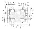
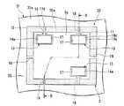
As shown in FIGS. 1 to 3, the
モールドシート3は、平面視略矩形の板状に形成されてモールドシート3の上面3aをなすステージ部(導電部)11と、マイクロフォンチップ5及びコンパニオンチップ7に電気接続される複数(図示例では3つ)のリード端子(導電部、他の端子)13と、これらステージ部11及びリード端子13をモールドする樹脂モールド部(絶縁部)15とを備えている。そして、ステージ部11及びリード端子13は、金属製薄板からなるリードフレームによって構成されており、導電性を有している。 The
ステージ部11の上面3aは樹脂モールド部15の表面15aから外方に露出しており、また、ステージ部11の下面11b及び側部は樹脂モールド部15によって覆われている。なお、本実施形態においては、ステージ部11の上面3aが樹脂モールド部15と同一平面を構成してマイクロフォンチップ5及びコンパニオンチップ7を搭載する一面となるモールドシート3の上面3aをなしている。
また、ステージ部11は、その周辺から内側に向けて切り欠き17を複数(図示例では3つ)形成してなり、各切り欠き17内にはリード端子13の一部が配されるようになっている。そして、各切り欠き17のうちその開口端17aにおける幅寸法は、開口端17aよりもステージ部11の内側に位置する各切り欠き17の底部よりも狭く形成されている。なお、この実施形態においては、2つの切り欠き17,17が矩形状のステージ部11の一辺(第1の辺)11cに並べて配されており、1つの切り欠き17が第1の辺11cと反対側に位置する一辺(第2の辺)11dに配されると共に、第1の辺11cに配された1つの切り欠き17に対向している。The
Further, the
さらに、ステージ部11には、その周辺から樹脂モールド部15の側面4まで一体に延びる吊リード19が複数(実施例では3つ)形成されており、これら吊リード19はステージ部11の上面3aと共に樹脂モールド部15の表面15aから外方に露出している。
なお、この実施形態においては、1つの吊リード19が第2の辺11dに形成されると共に第2の辺11dに形成された1つの切り欠き17に隣り合うように、かつ、第1の辺11cに形成された1つの切り欠き17に対向する位置に配されている。また、残り2つの吊リード19,19は、第1の辺11c及び第2の辺11dに直交するステージ部11の他の辺に1つずつ形成されており、互いに対向する位置に配されている。Furthermore, the
In this embodiment, one
また、ステージ部11には、その下面11bから突出するグランド用端子(一の端子)21が一体に形成されており、グランド用端子21の先端が樹脂モールド部15の外方に露出している。具体的には、グランド用端子21の外部接続面21bがモールドシート3の下面をなす樹脂モールド部15の裏面15bと共に同一平面を形成している。なお、このグランド用端子21は、半導体装置1を実装する実装基板のグランドパターン(不図示、外部配線)に半田付け等によって電気接続されるものである。 In addition, a ground terminal (one terminal) 21 protruding from the
各リード端子13は、ステージ部11の各切り欠き17内に配置されると共にコンパニオンチップ7に電気接続される内部配線用接続面(内部接続面)14aを有する接続部13aと、接続部13aからステージ部11の外方に向けて伸びる板状のサポートリード18とを有し、ステージ部11に接触しないように配されている。サポートリード18は、切り欠き17の開口端17aに配されると共にステージ部11の周縁から突出しており、樹脂モールド部15の側面4にその先端が露出するようになっている。また、サポートリード18は接続部13aよりも幅狭に形成されている。 Each
また、各リード端子13は、樹脂モールド部15から外方に露出して外部配線と電気的に接続される外部配線用接続面14bも有しており、外部配線用接続面14bは樹脂モールド部15の裏面15bと共に同一平面を形成している。なお、本実施形態においては、外部配線用接続面14bが接続部13a及びサポートリード18の全体にわたって形成されている。
以上のように構成された複数のリード端子13は、内部配線用接続面14a及び外部配線用接続面14bを一体に形成してなり、半導体装置1を実装基板(不図示)に実装する際に、半田付け等によりマイクロフォンチップ5及びコンパニオンチップ7を実装基板の接続端子(外部配線)に電気接続する外部接続端子としての役割を果たしている。Each
The plurality of
また、上述したステージ部11、サポートリード18及び吊リード19は、前述した金属製薄板にハーフエッチング加工を施して形成されるものであり、モールドシート3よりも薄く形成された部分を有している。
すなわち、リード端子13を構成するサポートリード18は、ステージ部11の上面3aや接続部13aの内部配線用接続面14aをなす金属製薄板の一方の主面から金属製薄板をエッチングして形成されており、元の金属製薄板の厚さ寸法の略半分に形成されている。これによって、サポートリード18がステージ部11の上面3aよりも下方に配される。すなわち、サポートリード18には、その全体にわたってモールドシート3のうち後述する蓋体9を搭載する面から窪む窪み部24が形成されている。Further, the
That is, the
また、ステージ部11及び吊リード19は、金属製薄板の他方の主面から金属製薄板をエッチングして形成されており、元の金属製薄板の厚さ寸法の略半分に形成されている。なお、ステージ部11のうちグランド用端子21の形成部分には、前述のハーフエッチング加工が施されておらず、グランド用端子21とあわせて元の金属製薄板と同じ厚さ寸法となっている。すなわち、グランド用端子21の形成部分は、切り欠き17内に形成された樹脂モールド部15と同じ厚さとなっている。また、リード端子13の接続部13aにもハーフエッチング加工が施されておらず、これも元の金属製薄板と同じ厚さ寸法となっている。 Moreover, the
樹脂モールド部15は、電気的な絶縁材料からなり、ステージ部11の下面11b、吊リード19の下側、及び、サポートリード18の窪み部24上に形成されると共に、ステージ部11と切り欠き17内に配されたリード端子13との隙間を埋めるように形成されている。また、樹脂モールド部15は、ステージ部11の上面3a及びリード端子13の内部配線用接続面14aを表面15aから外方に露出させるように、さらに、リード端子13の外部配線用接続面14b及びグランド用端子21の外部接続面21bを裏面15bから外方に露出させるように形成されている。
したがって、ステージ部11と切り欠き17内のリード端子13との隙間に配された樹脂モールド部15の厚み寸法は、前述したハーフエッチング加工を施す前の金属製薄板と同等になり、モールドシート3の厚み寸法が金属製薄板と等しくなる。The
Therefore, the thickness dimension of the
蓋体9は、例えば銅材などの導電性材料を箱型の有底略筒状に形成してなり、ステージ部11の上面3a及びサポートリード18の窪み部24上に形成された樹脂モールド部15上にわたって配されている。すなわち、蓋体9の開口端9aがステージ部11の上面3aの周縁及び切り欠き17の開口端17a内に形成された樹脂モールド部15上にわたって配されている。これにより、ここで、蓋体9の開口端9aは、導電性接着剤32によってステージ部11の上面3aに接着固定されており、これにより、ステージ部11と蓋体9とが電気接続されることになる。
なお、切り欠き17の開口端17aに配されたサポートリード18は、ステージ部11の上面3aと同一平面をなす樹脂モールド部15によって覆われてステージ部11の上面3a側から露出しないため、各リード端子13と蓋体9とは電気的に絶縁されることになる。The
In addition, since the
そして、このように蓋体9を配置することで、蓋体9が前述のモールドシート3と共にマイクロフォンチップ5及びコンパニオンチップ7を含む中空の空洞部S1が形成される。すなわち、蓋体9はモールドシート3と共に中空の空洞部S1を有するハウジングを形成することになる。
また、ステージ部11の上面3a及びリード端子13を構成する接続部13aの内部配線用接続面14aは、樹脂モールド部15から前述の空洞部S1に露出している。すなわち、ステージ部11と電気的に絶縁された内部配線用接続面14aが、ハウジング内に露出している。そして、蓋体9には、前述の空洞部S1を外方に連通させる音響孔9bが形成されている。And by arrange | positioning the
Further, the
マイクロフォンチップ5は、シリコン等からなり、音響等の圧力変動を電気信号に変換するものであり、圧力変動に応じて振動する音響検出部5aを有している。また、このマイクロフォンチップ5は、音響検出部5aの振動を電気抵抗の変化として捉え、これら容量や抵抗の変化を電気信号として取り出すように構成されている。
そして、マイクロフォンチップ5は、音響検出部5aがステージ部11の上面3aに対向するように、絶縁性接着ペースト(不図示)を介してステージ部11に接着固定されている。これにより、マイクロフォンチップ5の音響検出部5aとステージ部11の上面3aとの間に空洞部S2が形成される。The
The
コンパニオンチップ7は、マイクロフォンチップ5を駆動制御する役割を果たすものであり、例えばマイクロフォンチップ5からの電気信号を増幅するための増幅回路や、前記電気信号をデジタル信号として処理するためのA/D変換器、DSP(デジタルシグナルプロセッサ)、等を含んで構成されている。このコンパニオンチップ7は、マイクロフォンチップ5の場合と同様の絶縁性接着ペースト(不図示)を介してステージ部11の上面3aに固定されている。 The
そして、コンパニオンチップ7は、内部配線をなす第1のワイヤー23によってマイクロフォンチップ5と電気的に接続されており、内部配線をなす第2のワイヤー25によりリード端子13の内部配線用接続面14aに電気接続されている。また、コンパニオンチップ7は、第3のワイヤー27によりステージ部11の上面3aに電気接続されている。これにより、マイクロフォンチップ5がリード端子13及びステージ部11と電気的に接続されることになる。
以上のように構成された半導体装置1は、音響等の圧力変動を音響孔9bから空洞部S1内に導入すると共に音響検出部5aに到達させることで、上記圧力変動を検出するマイクロフォンパッケージを構成している。The
The
次に、この半導体装置1の製造方法について、以下に説明する。
本実施形態の半導体装置1を製造する場合には、はじめに、モールドシート3を製造する(モールドシート製造工程)。このモールドシート製造工程においては、はじめに、図4,5に示すように、銅材等からなる金属製薄板31にプレス加工やエッチング加工を施して、枠部35の内側に複数のリード端子13及び吊リード19を突出させると共に、吊リード19を枠部35の内側に配される平面視略矩形状のステージ部11に一体に連結させた構成のリードフレーム33を形成する(リードフレーム形成工程)。すなわち、このリードフレーム33においては、枠部35及び吊リード19がステージ部11及びリード端子13を一体に連結する連結部をなしている。Next, a method for manufacturing the
When manufacturing the
また、このリードフレーム形成工程においては、ステージ部11に金属製薄板31の一方の主面31aからなるステージ部11の上面3aの周縁から内側に向けて切り欠いた切り欠き17が形成され、リード端子13の接続部13a及びサポートリード18の一部がステージ部11に接触しないように切り欠き17内に配置される。すなわち、略板状のステージ部11には、その周辺から内側に向けて複数の切り欠き17が形成され、リード端子13の接続面14a,14b側がステージ部11と電気的に絶縁して樹脂モールドできるように間隔を保ちながら、切り欠き17内に配置されている。 Further, in this lead frame forming step, a
そして、リード端子13のサポートリード18、ステージ部11及び吊リード19には、ハーフエッチング加工が施される(ハーフエッチング工程)。このハーフエッチング工程においては、金属製薄板31の一方の主面31a側からハーフエッチング加工を施して、サポートリード18全体(図4におけるハッチング部分)を元の金属製薄板31よりも薄く形成する。すなわち、サポートリード18には、その全体にわたって前記蓋体9が搭載される面よりも窪む窪み部が形成されている。 The
また、この工程においては、金属製薄板31の他方の主面31b側からハーフエッチング加工を施して、グランド用端子21の形成部分を除くステージ部11及び吊リード19(図5におけるハッチング部分)を元の金属製薄板31よりも薄く形成する。
なお、このハーフエッチング工程は、前述のリードフレーム形成工程と同時に行われるとしてもよいし、リードフレーム形成工程の前後に実施されるとしても構わない。そして、このリードフレーム33は、1つの金属製薄板31に1つだけ形成されるとしてもよいし、複数連ねて形成されるとしても構わない。Further, in this step, half etching processing is performed from the other
This half-etching process may be performed simultaneously with the above-described lead frame forming process, or may be performed before and after the lead frame forming process. Then, only one
そして、これらリードフレーム形成工程及びハーフエッチング工程の終了後には、図6〜8に示すように、リードフレーム33を樹脂モールド部15により樹脂モールドする(モールド工程)。このモールド工程においては、樹脂モールド部形成用の金型によってリードフレーム33をその厚さ方向から挟み込むことで、ハーフエッチング工程においてリードフレーム33のうち元の金属製薄板31よりも薄く形成された部分と、金型の内面とによってキャビティが形成されることになる。そして、このキャビティ内に樹脂(絶縁材料)を充填することで樹脂モールド部15が形成されることになる。
最後に、樹脂モールド部15によってモールドされたリード端子13及び吊リード19を樹脂モールド部15の外側に位置する枠部35から切り離す(切断工程)ことで、モールドシート3の製造が完了する。なお、この切り離しは、ステージ部11と枠部35の間に形成された樹脂モールド部15を切断し、その切断面には、サポートリード18及び吊リード19の先端が露出する。And after completion | finish of these lead frame formation processes and a half etching process, as shown to FIGS. 6-8, the
Finally, the
なお、図6におけるハッチング部分はステージ部11の上面3a側から見た場合の樹脂モールド部15の形成部分を示しており、図6,8に示すように、ステージ部11の上面3a、リード端子13を構成する接続部13aの内部配線用接続面14a及び吊リード19が樹脂モールド部15から露出し、樹脂モールド部15の表面15aと共に同一平面を形成している。また、ステージ部11と枠部35との隙間、及び、ステージ部11と切り欠き17内に配された接続部13a及びサポートリード18との隙間にも樹脂が充填され、さらに、サポートリード18の上側が樹脂モールド部15によって覆われている。 The hatched portion in FIG. 6 shows a portion where the
また、図7におけるハッチング部分はステージ部11の下面側から見た場合の樹脂モールド部15の形成部分を示しており、図7,8に示すように、リード端子13の外部配線用接続面14b及びグランド用端子21の外部接続面21bが樹脂モールド部15から露出し、樹脂モールド部15の裏面15bと共に同一平面を形成している。また、ステージ部11の下面11b及び吊リード19の下側が樹脂モールド部15によって覆われている。
すなわち、このモールドシート製造工程においては、元の金属製薄板31と同じ厚さ寸法のモールドシート3が製造されることになる。Further, the hatched portion in FIG. 7 indicates a portion where the
That is, in this mold sheet manufacturing process, the
そして、モールドシート製造工程後には、図1〜3に示すように、モールドシート3の上面3aをなすステージ部11に絶縁性の接着ペースト(不図示)を介してマイクロフォンチップ5及びコンパニオンチップ7を固定する(チップ配置工程)。また、ワイヤーボンディングによりマイクロフォンチップ5とコンパニオンチップ7を第1のワイヤー23で電気接続すると共に、コンパニオンチップ7とリード端子13の内部配線用接続面14a及びステージ部11の上面3aとを第2のワイヤー25及び第3のワイヤー27で電気接続する(電気接続工程)。 After the mold sheet manufacturing process, as shown in FIGS. 1 to 3, the
最後に、蓋体9がマイクロフォンチップ5及びコンパニオンチップ7の上方を覆うように、蓋体9の開口端9aをステージ部11の上面3aの周縁に固定する(蓋体配置工程)ことで、半導体装置1の製造が完了する。
なお、この蓋体配置工程においては、蓋体9の固定が導電性接着剤32によって行われる。また、この蓋体配置工程においては、蓋体9の開口端9aが切り欠き17の開口端17aにおいてその幅方向にわたって配されるが、切り欠き17の開口端17aに配されるサポートリード18はその全体が窪み部24に形成されてステージ部11の上面3aよりも下方に配されている。また、窪み部24に形成されたサポートリード18の上方は樹脂モールド部15によって覆われるため、リード端子13が蓋体9に接触することを容易に防止できる。
なお、この半導体装置1の製造方法においては、前述したモールドシート製造工程の切断工程が、例えばチップ配置工程後から蓋体配置工程後までの間に行われるとしても構わない。Finally, the
In this lid body arranging step, the
In the method for manufacturing the
そして、以上のように製造された半導体装置1を実装基板(不図示)に実装する際には、樹脂モールド部15の裏面15bを実装基板の表面に対向させた状態で、半田付け等によりリード端子13及びグランド用端子21を実装基板のランドに電気接続すればよい。
これにより、蓋体9及びステージ部11が実装基板のグランドパターンに電気接続することができ、蓋体9及びステージ部11によって空洞部S1内へのノイズの侵入を遮断するシールド部が形成されることになる。ここで、シールド部は、蓋体9とステージ部11とが接触しない切り欠き17及び蓋体9に形成された音響孔9bを除いて空洞部S1全体を覆うため、ノイズが空洞部S1内に侵入する隙間領域を最小限に抑えることができる。したがって、この実施形態にかかる半導体装置1及びリードフレーム33によれば、そのシールド性向上を図ることができる。When the
Accordingly, the
また、この半導体装置1及びリードフレーム33によれば、ステージ部11や吊リード19、リード端子13のサポートリード18にハーフエッチング加工を施してリードフレーム33を形成し、リード端子13等に折り曲げ部分が存在しないため、モールド工程において金型によりリードフレーム33をその厚さ方向から挟み込む際に、ステージ部11及びリード端子13が変形することを防止できるため、半導体装置1を容易に製造することができる。
すなわち、プレス加工によりリード端子13を折り曲げたり、吊リード19を折り曲げてステージ部11をアップセットする等して、先端部13aを除くリード端子13をステージ部11の上面3aよりも下方に配する場合には、モールド工程において金型によりステージ部11及びリード端子13を挟み込む際に、リード端子13や吊リード19の折り曲げ部分が変形してステージ部11やリード端子13の一部が金型の内面から離れる場合があるため、ステージ部11や吊リード19、リード端子13と樹脂モールド部15との境界に樹脂のバリが形成される。Further, according to the
That is, the
これに対して、上記実施形態のように先端部13aを除くリード端子13やステージ部11を金属製薄板よりも薄く形成した場合には、前述したようにモールド工程においてステージ部11及びリード端子13の変形を防止できるため、上述したバリの発生を容易に防止できる。
また、ステージ部11及びリード端子13をモールドする樹脂モールド部15の厚み寸法を金属製薄板31と同等に形成することもできるため、半導体装置1の薄型化を容易に図ることができる。On the other hand, when the
Moreover, since the thickness dimension of the
さらに、ステージ部11の下面11bに突出して形成されたグランド用端子21の周囲に樹脂モールド部15を形成することで、このグランド用端子21によってステージ部11が樹脂モールド部15と噛み合うことになる。すなわち、ステージ部11と樹脂モールド部15との密着力を向上させて、ステージ部11が樹脂モールド部15から剥離することを容易に防止できる。
なお、ステージ部11と樹脂モールド部15との密着力を向上させる他の手法としては、例えばマイクロフォンチップ5及びコンパニオンチップ7の配置領域を除くステージ部11にその厚さ方向に貫通する貫通孔を形成しておき、この貫通孔内にも樹脂モールド部15を形成することが挙げられる。この場合には、貫通孔内に充填された樹脂によるアンカー効果によってステージ部11と樹脂モールド部15との密着力をさらに向上させることができる。なお、貫通孔の形成位置は、半導体装置1のシールド性が低下しない位置に形成されることが望ましい。Further, by forming the
As another method for improving the adhesion between the
そして、上記実施形態において、リード端子13の接続部13aは、エッチング前の金属製薄板と同じ厚さ寸法を有するとしたが、これに限ることはなく、例えば図9に示すように、外部配線用接続面14bから窪むように元の金属製薄板の厚さ寸法の略半分に形成されるとしても構わない。すなわち、リード端子13の外部配線用接続面14bの周辺にモールドシート3の裏面15bから窪む段差が形成されるとしてもよい。この場合には、上記実施形態のように、接続部13aと一体に形成されたサポートリード18の窪み部24上に樹脂モールド部15が形成されることに加え、接続部13aの下側にも樹脂モールド部15が形成されるため、リード端子13が樹脂モールド部15によってその厚さ方向から挟み込まれることになる。したがって、リード端子13と樹脂モールド部15との密着力を向上させて、リード端子13が樹脂モールド部15から剥離することを容易に防止できる。 In the above embodiment, the connecting
また、ステージ部11に一体に形成される吊リード19は、樹脂モールド部15の表面15aから外方に露出するとしたが、これに限ることは無く、例えば図10に示すように、樹脂モールド部15の表面15aから外方に露出させずに、樹脂モールド部15の裏面15bから外方に露出させるとしても構わない。すなわち、吊リード19には、上記実施形態のサポートリード18と同様に、金属製薄板の一方の主面側からハーフエッチング加工が施されるとしてもよい。すなわち、吊リード19はその一面が蓋体9を搭載する面よりも窪むように形成されていればよい。
この場合には、吊リード19の上側及びステージ部11の下側に樹脂モールド部15が形成されるため、すなわち、一体に形成されたステージ部11及び吊リード19が樹脂モールド部15によってその厚さ方向から挟み込まれることになるため、ステージ部11と樹脂モールド部15との密着力の向上をさらに図ることができる。Further, the
In this case, since the
さらに、この場合には、リードフレームの状態において、枠部35に連結される吊リード19が、ステージ部11の周縁から外側に突出するサポートリード18と同様に、樹脂モールド部15の裏面15bから露出するため、モールドシート3の製造において、プレス加工によりモールドシート3の個片化を容易かつ迅速に行うことができる。すなわち、半導体装置の製造効率の向上を図ることができる。
また、このように吊リード19を形成する場合には、例えば図示例のようにグランド用端子21に連ねて形成されるとしても構わない。Further, in this case, in the state of the lead frame, the
Further, when the
さらに、複数のリード端子13は、平面視略矩形状に形成されたステージ部11の第1の辺11c及び第2の辺11dに配されるとしたが、これに限ることは無く、例えばステージ部11の第1の辺11cのみに並べて配されるとしてもよい。この場合には、ステージ部11の残りの三辺にリード端子13が配されないため、すなわち、リード端子13を配するための切り欠き17を形成する必要が無くなり、ステージ部11の残りの三辺には切り欠き17に基づくステージ部11と蓋体9との隙間が形成されない。これにより、ステージ部11の三辺から空洞部S1内へのノイズの侵入を遮断することができる。
なお、この場合には、ステージ部11の第2の辺11dの近傍に、ステージ部11の下面11bから突出する上記実施形態と同様のグランド用端子を第2の辺11dに沿って複数配列することが好ましい。このように複数のグランド用端子を配列することで、半導体装置を実装基板に安定した状態で実装することが可能となる。Furthermore, although the plurality of
In this case, a plurality of ground terminals similar to those in the above-described embodiment protruding from the
また、マイクロフォンチップ5やコンパニオンチップ7は、絶縁性接着ペーストによってステージ部11の上面3aに固定されるとしたが、これに限ることは無く、少なくともステージ部11の上面3a上に搭載されていればよい。すなわち、例えばステージ部11の上面3aに樹脂からなる台座用モールド部を形成し、台座用モールド部の上面にマイクロフォンチップ5やコンパニオンチップ7が固定されるとしても構わない。
この台座用モールド部は、例えばモールドシート3の製造工程において樹脂モールド部15と同時に形成されるとしてもよい。ただし、台座用モールド部は、ステージ部11の上面3aのうち少なくとも蓋体9の開口端9aの配置領域を避けるように形成する必要がある。In addition, the
This pedestal mold part may be formed simultaneously with the
さらに、蓋体9の開口端9aは、ステージ部11の上面3aの周縁に配されるとしたが、これに限ることは無く、少なくともマイクロフォンチップ5、コンパニオンチップ7及びリード端子13の内部配線用接続面14aが空洞部S1内に含まれるようにステージ部11の上面3aに配されていればよい。すなわち、蓋体9の開口端9aは、少なくともリード端子13と電気的に絶縁されるようにステージ部11の一部と電気的に接続していればよい。さらに、蓋体9の開口端9aは、リード端子13の内部配線用接続面14aやマイクロフォンチップ5、コンパニオンチップ7の配置領域を除けば、例えばステージ部11の周縁よりも内側に配されるとしても構わない。 Further, the opening
また、蓋体9の開口端9aは、吊リード19と接触すると共に、ステージ部11の上面3aに接続されていてもよいし、蓋体9の開口端9aとステージ部11の上面3aとの間に導電部材を配置しておき、蓋体9の開口端9aが、吊リード19と接触すると共に、ステージ部11の上面3aと接続する導電部材を介してステージ部11の上面3aに電気的に接続されるとしてもよい。これらの場合には、蓋体9とステージ部11との接触部分が増えることから、蓋体9とステージ部11との固定の信頼性が増す。 Further, the opening
さらに、蓋体9は、導電性接着剤32によってモールドシート3に固定されるとしたが、これに限ることはない。蓋体9は、例えば、半田によってモールドシート3に固定することもできる。この場合、蓋体9は、マイクロフォンチップ5及びコンパニオンチップ7を搭載し、これらと電気接続されたモールドシート3を実装基板にリフロー工程にて半田付けすると同時にモールドシート3に固定することも可能となる。
また、リード端子13の窪み部24は、サポートリード18の全体にわたって形成されるとしたが、蓋体9がサポートリード18に接触しなければ、サポートリード18の一部のみに形成されていてもよい。すなわち、蓋体9が上記実施形態のように配される場合、窪み部24は、切り欠き17の開口端17aに配されるサポートリード18の幅方向にわたって形成されていればよい。Furthermore, although the
In addition, the
さらに、サポートリード18は、その一部が切り欠き17の外側に突出するとしたが、例えば全体が切り欠き17に配されるとしても構わない。ステージ部11の各切り欠き17内には各リード端子13の一部が配されるとしたが、これに限ることは無く、例えば各リード端子13の全体が配されるとしても構わない。
また、上記実施形態のリードフレーム33は、これにハーフエッチング加工を施して形成されるとしたが、モールドシート3の薄型化や樹脂のバリを考慮しない場合には、例えばプレス加工を施す、すなわちリード端子13に折り曲げ加工を施す等して形成されるとしても構わない。この場合でも、上記実施形態の窪み部24と同様に、サポートリード18にステージ部11の上面3aの下方に配される窪み部を形成することができる。
さらに、空洞部S1を外方に連通させる音響孔9bは、蓋体9に形成されるとしたが、これに限ることはなく、例えばモールドシート3に形成されるとしても構わない。Furthermore, although the
In addition, the
Furthermore, although the
また、複数のリード端子13及びグランド用端子21は、樹脂モールド部15の裏面15bから外側に露出するとしたが、少なくとも実装基板に電気接続させるようにモールドシート3の外側に露出していればよく、例えばモールドシート3の側面4から外側に突出するとしてもよい。この場合、グランド用端子21は吊リード19により構成すればよい。
また、半導体装置1は、ステージ部11の上面3aにコンパニオンチップ7を設けて構成されるとしたが、少なくともマイクロフォンチップ5を設けて構成されていればよい。なお、この場合には、半導体装置1を実装する実装基板にコンパニオンチップ7を別途搭載すると共に、実装基板を介して半導体装置1とコンパニオンチップ7とを電気接続すればよい。Further, the plurality of
In addition, the
さらに、上記実施形態においては、圧力変動を検出するマイクロフォンチップ5を備える半導体装置1について説明したが、少なくともモールドシート3及び蓋体9により半導体センサチップを含む中空の空洞部S1を形成した構成の半導体装置に適用することができる。すなわち、モールドシート3や蓋体9に音響孔9bが形成されていない構成の半導体装置にも適用することができ、外方に対して密閉された空洞部S1内に配する半導体センサチップとしては、例えば加速度センサチップが挙げられる。 Furthermore, in the above embodiment, the
以上、本発明の実施形態について図面を参照して詳述したが、具体的な構成はこの実施形態に限られるものではなく、本発明の要旨を逸脱しない範囲の設計変更等も含まれる。 As mentioned above, although embodiment of this invention was explained in full detail with reference to drawings, the concrete structure is not restricted to this embodiment, The design change etc. of the range which does not deviate from the summary of this invention are included.
1…半導体装置(マイクロフォンパッケージ)、3…モールドシート、3a…上面、4…側面、5…マイクロフォンチップ(半導体センサチップ)、5a…音響検出部、9…蓋体、9a…開口端、9b…音響孔、11…ステージ部(導電部)、11b…下面、13…リード端子13(導電部、他の端子)、13a…接続部、14a…内部配線用接続面(内部接続面)、14b…外部配線用接続面、15…樹脂モールド部(絶縁部)、17…切り欠き、18…サポートリード、19…吊リード(連結部)、21…グランド用端子(突起部、一の端子)、21b…外部接続面、23…第1のワイヤー(内部配線)、24…窪み部、25…第2のワイヤー(内部配線)、31…金属製薄板、31a…一方の主面、31b…他方の主面、33…リードフレーム、35…枠部(連結部)、S1…空洞部DESCRIPTION OF
Claims (9)
Translated fromJapanese前記モールドシートが、略板状に形成されて前記上面をなすと共に周辺から内側に向けて複数の切り欠きを形成した導電性のステージ部と、少なくとも一部が各切り欠き内に配置されて前記半導体センサチップと電気接続される導電性の複数のリード端子と、前記ステージ部及び前記リード端子を相互に電気的に絶縁させるように樹脂モールドする絶縁部と、を備え、
前記リード端子が、前記切り欠き内に配置されると共に前記空洞部に露出して前記半導体センサチップに電気接続する内部接続面を有する接続部と、該接続部から前記ステージ部の外方に向けて伸び、前記モールドシートの側面にその先端が露出するサポートリードと、を備え、
少なくとも前記サポートリードのうち前記切り欠き内に配される部分に、その幅方向にわたって前記上面よりも下方に配される窪み部が形成され、
該窪み部上に前記絶縁部が形成され、
前記蓋体の開口端が、前記ステージ部の上面、及び、前記窪み部上に形成された前記絶縁部上の両方に配されていることを特徴とする半導体装置。A mold sheet formed in a plate shape, a semiconductor sensor chip mounted on the upper surface of the mold sheet, and having conductivity, including the semiconductor sensor chip together with the mold sheet so as to cover the upper side of the semiconductor sensor chip A bottomed substantially cylindrical lid that forms a hollow cavity, and
The mold sheet is formed in a substantially plate shape to form the upper surface and a plurality of cutouts from the periphery to the inside, and at least a part thereof is disposed in each cutout. A plurality of conductive lead terminals electrically connected to the semiconductor sensor chip, and an insulating part that is resin-molded so as to electrically insulate the stage part and the lead terminals from each other,
The lead terminal is disposed in the notch and is exposed to the cavity and has an internal connection surface that is electrically connected to the semiconductor sensor chip, and the connection portion is directed outward from the stage portion. A support lead whose tip is exposed on the side surface of the mold sheet,
At least a portion of the support lead that is disposed in the notch is formed with a recess that is disposed below the upper surface over the width direction thereof.
The insulating part is formed on the hollow part,
An opening end of the lid is arranged on both the upper surface of the stage portion and the insulating portion formed on the recess portion .
前記窪み部が、前記ステージ部の上面をなす前記金属製薄板の一方の主面から前記金属製薄板をエッチングして形成され、
前記ステージ部が、前記金属製薄板の他方の主面から前記金属製薄板をエッチングして形成され、
前記ステージ部の下面に前記絶縁部が形成されていることを特徴とする請求項1に記載の半導体装置。The stage part and the lead terminal are constituted by a lead frame made of a thin metal plate,
The recess is formed by etching the metal thin plate from one main surface of the metal thin plate forming the upper surface of the stage portion,
The stage portion is formed by etching the metal thin plate from the other main surface of the metal thin plate,
The semiconductor device according to claim 1, wherein the insulating portion is formed on a lower surface of the stage portion.
前記接続部の下側に前記絶縁部が形成されていることを特徴とする請求項2に記載の半導体装置。The connecting portion is formed by etching the metal thin plate from the other main surface of the metal thin plate,
The semiconductor device according to claim 2, wherein the insulating portion is formed below the connecting portion.
前記グランド用端子の外部接続面が、前記ステージ部の下面に形成された前記絶縁部から外方に露出していることを特徴とする請求項1から請求項3のいずれか1項に記載の半導体装置。The mold sheet is formed integrally with the stage portion so as to protrude from the lower surface of the stage portion, and includes a conductive ground terminal electrically connected to the semiconductor sensor chip,
4. The external connection surface of the ground terminal is exposed to the outside from the insulating portion formed on the lower surface of the stage portion. 5. Semiconductor device.
前記蓋体に、前記空洞部を外方に連通させる音響孔が形成されていることを特徴とする請求項1から請求項4のいずれか1項に記載の半導体装置。The semiconductor sensor chip comprises a microphone chip having an acoustic detection unit that detects pressure fluctuations by vibrations,
5. The semiconductor device according to claim 1, wherein an acoustic hole that allows the cavity to communicate outward is formed in the lid. 6.
前記導電部は、前記マイクロフォンチップを搭載する一面を有すると共にその周辺から内側に向けて複数の切り欠きが形成された板状のステージ部と、配線と電気的に接続される接続面を有する複数の端子と、からなり、
これら複数の端子は、前記ステージ部と一体に形成された一の端子と、少なくとも前記絶縁部によって前記ステージ部と電気的に絶縁されるように前記切り欠き内に配置された他の端子と、を備え、
前記モールドシートは、少なくとも前記ステージ部の一面と前記複数の端子の接続面とを露出させるように、前記ステージ部及び前記他の端子を前記絶縁部によって樹脂モールドしてなり、
前記蓋体は、前記マイクロフォンチップと前記配線によって電気接続される前記他の端子の接続面が前記ハウジング内に露出するように、前記他の端子と電気的に絶縁された状態で前記ステージ部と電気的に接続されることを特徴とするマイクロフォンパッケージ。A plate-shaped mold sheet composed of a conductive part and an insulating part, a lid that forms a housing having conductivity and a hollow cavity and an acoustic hole together with the mold sheet, and a microphone chip disposed in the housing And comprising
The conductive portion has a surface on which the microphone chip is mounted, a plate-like stage portion in which a plurality of notches are formed from the periphery to the inside, and a plurality of connection surfaces that are electrically connected to the wiring. The terminal and
The plurality of terminals are one terminal formed integrally with the stage part, and another terminal disposed in the notch so as to be electrically insulated from the stage part by at least the insulating part, With
The mold sheet is formed by resin-molding the stage part and the other terminals with the insulating part so as to expose at least one surface of the stage part and connection surfaces of the plurality of terminals.
The lid body is electrically insulated from the other terminal so that a connection surface of the other terminal electrically connected to the microphone chip by the wiring is exposed in the housing. A microphone package characterized by being electrically connected.
前記他の端子は、前記ステージ部の内方から外方に向けて伸び、前記モールドシートの側面にその先端が露出するサポートリードを有し、
該サポートリードには、前記モールドシートのうち前記蓋体を搭載する面から窪む窪み部が形成され、
該窪み部上に前記絶縁部が形成されていることを特徴とする請求項6に記載のマイクロフォンパッケージ。The conductive portion is constituted by a lead frame,
The other terminal has a support lead that extends from the inside of the stage portion to the outside and the tip of the mold sheet is exposed on the side surface of the mold sheet.
The support lead is formed with a recessed portion that is recessed from the surface of the mold sheet on which the lid is mounted,
The microphone package according toclaim 6 , wherein the insulating portion is formed on the hollow portion.
該吊リードは、前記蓋体に接触していることを特徴とする請求項7に記載のマイクロフォンパッケージ。The stage portion extends outward from the periphery thereof, and has a suspension lead whose tip is exposed on the side surface of the mold sheet,
The microphone package according toclaim 7 , wherein the suspension lead is in contact with the lid.
前記他の端子は、前記枠部に接合するサポートリードを有し、
該サポートリードには、ハーフエッチングが施されることにより前記蓋体を搭載する面から窪む窪み部が形成されており、
前記ステージ部は、その周辺から外方に向けて伸び、前記モールドシートの側面に先端が露出する吊リードを有し、
前記モールドシートは、前記窪み部上に絶縁部が形成されるように前記リードフレームを樹脂モールドし、前記吊リードを含む面において切断することで形成されることを特徴とする請求項6に記載のマイクロフォンパッケージ。The conductive portion is constituted by a lead frame including a frame portion,
The other terminal has a support lead joined to the frame portion,
The support lead is formed with a recess that is recessed from the surface on which the lid is mounted by being half-etched.
The stage portion extends outward from the periphery thereof, and has a suspension lead whose tip is exposed on the side surface of the mold sheet,
The mold sheet according toclaim 6, said lead frame as an insulating portion on the recess portion is formed by resin molding, characterized in that it is formed by cutting in a plane including said interconnection leads Microphone package.
Priority Applications (6)
| Application Number | Priority Date | Filing Date | Title |
|---|---|---|---|
| JP2007206724AJP4380748B2 (en) | 2007-08-08 | 2007-08-08 | Semiconductor device and microphone package |
| US12/221,572US20090065882A1 (en) | 2007-08-08 | 2008-08-05 | Semiconductor device, lead frame, and microphone package therefor |
| KR1020080076271AKR100966681B1 (en) | 2007-08-08 | 2008-08-05 | Semiconductor device, lead frame and its microphone package |
| EP08014088AEP2023658A2 (en) | 2007-08-08 | 2008-08-06 | Semiconductor device, lead frame, and microphone package therefor |
| CN2008101461137ACN101362585B (en) | 2007-08-08 | 2008-08-06 | Semiconductor device, lead frame, and microphone package therefor |
| TW097129923ATW200926363A (en) | 2007-08-08 | 2008-08-06 | Semiconductor device, lead frame, and microphone package therefor |
Applications Claiming Priority (1)
| Application Number | Priority Date | Filing Date | Title |
|---|---|---|---|
| JP2007206724AJP4380748B2 (en) | 2007-08-08 | 2007-08-08 | Semiconductor device and microphone package |
Publications (2)
| Publication Number | Publication Date |
|---|---|
| JP2009043894A JP2009043894A (en) | 2009-02-26 |
| JP4380748B2true JP4380748B2 (en) | 2009-12-09 |
Family
ID=39951691
Family Applications (1)
| Application Number | Title | Priority Date | Filing Date |
|---|---|---|---|
| JP2007206724AActiveJP4380748B2 (en) | 2007-08-08 | 2007-08-08 | Semiconductor device and microphone package |
Country Status (6)
| Country | Link |
|---|---|
| US (1) | US20090065882A1 (en) |
| EP (1) | EP2023658A2 (en) |
| JP (1) | JP4380748B2 (en) |
| KR (1) | KR100966681B1 (en) |
| CN (1) | CN101362585B (en) |
| TW (1) | TW200926363A (en) |
Families Citing this family (12)
| Publication number | Priority date | Publication date | Assignee | Title |
|---|---|---|---|---|
| US8148808B2 (en)* | 2007-08-13 | 2012-04-03 | Lv Sensors, Inc. | Partitioning of electronic packages |
| KR101074732B1 (en)* | 2010-12-14 | 2011-10-18 | 주식회사 비에스이 | Vacuum adsorption mounted condenser microphone structure and its mounting method |
| CN103367615B (en)* | 2012-04-06 | 2018-02-02 | 日亚化学工业株式会社 | Light-emitting device is with being packaged into body and used its light-emitting device |
| US8836110B2 (en)* | 2012-08-31 | 2014-09-16 | Freescale Semiconductor, Inc. | Heat spreader for use within a packaged semiconductor device |
| DE102013217888B4 (en)* | 2012-12-20 | 2024-07-04 | Continental Automotive Technologies GmbH | Electronic device and method for manufacturing an electronic device |
| US20140208689A1 (en) | 2013-01-25 | 2014-07-31 | Renee Joyal | Hypodermic syringe assist apparatus and method |
| US10551011B2 (en)* | 2013-01-25 | 2020-02-04 | Lumileds Llc | Lighting assembly and method for manufacturing a lighting assembly |
| JP2015005597A (en)* | 2013-06-20 | 2015-01-08 | 日立オートモティブシステムズ株式会社 | Resin sealed type sensor device |
| KR101598270B1 (en)* | 2014-03-03 | 2016-02-26 | 삼성전기주식회사 | Microphone package |
| US20150296306A1 (en)* | 2014-04-10 | 2015-10-15 | Knowles Electronics, Llc. | Mems motors having insulated substrates |
| DE102015216217A1 (en)* | 2015-08-25 | 2017-03-02 | Continental Teves Ag & Co. Ohg | Method of encasing an electrical unit and electrical component |
| US10327060B2 (en)* | 2017-11-05 | 2019-06-18 | xMEMS Labs, Inc. | Air pulse generating element and sound producing device |
Family Cites Families (7)
| Publication number | Priority date | Publication date | Assignee | Title |
|---|---|---|---|---|
| JP2007012895A (en) | 2005-06-30 | 2007-01-18 | Sanyo Electric Co Ltd | Circuit device and manufacturing method thereof |
| US7646092B2 (en) | 2005-12-06 | 2010-01-12 | Yamaha Corporation | Semiconductor device and manufacturing method thereof |
| JP4652281B2 (en) | 2006-05-29 | 2011-03-16 | パナソニック株式会社 | Resin-sealed semiconductor device |
| US7550828B2 (en)* | 2007-01-03 | 2009-06-23 | Stats Chippac, Inc. | Leadframe package for MEMS microphone assembly |
| US7777310B2 (en)* | 2007-02-02 | 2010-08-17 | Stats Chippac Ltd. | Integrated circuit package system with integral inner lead and paddle |
| JP2007206724A (en) | 2007-04-20 | 2007-08-16 | Hitachi Displays Ltd | Liquid crystal display device and driving method thereof |
| US8507319B2 (en)* | 2007-12-07 | 2013-08-13 | Stats Chippac Ltd. | Integrated circuit package system with shield |
- 2007
- 2007-08-08JPJP2007206724Apatent/JP4380748B2/enactiveActive
- 2008
- 2008-08-05KRKR1020080076271Apatent/KR100966681B1/ennot_activeExpired - Fee Related
- 2008-08-05USUS12/221,572patent/US20090065882A1/ennot_activeAbandoned
- 2008-08-06EPEP08014088Apatent/EP2023658A2/ennot_activeWithdrawn
- 2008-08-06CNCN2008101461137Apatent/CN101362585B/ennot_activeExpired - Fee Related
- 2008-08-06TWTW097129923Apatent/TW200926363A/enunknown
Also Published As
| Publication number | Publication date |
|---|---|
| TW200926363A (en) | 2009-06-16 |
| KR20090015823A (en) | 2009-02-12 |
| CN101362585A (en) | 2009-02-11 |
| US20090065882A1 (en) | 2009-03-12 |
| CN101362585B (en) | 2011-12-14 |
| EP2023658A2 (en) | 2009-02-11 |
| JP2009043894A (en) | 2009-02-26 |
| KR100966681B1 (en) | 2010-06-29 |
Similar Documents
| Publication | Publication Date | Title |
|---|---|---|
| JP4380748B2 (en) | Semiconductor device and microphone package | |
| JP2009164475A (en) | Microphone package, lead frame, mold substrate, and mounting structure of microphone package | |
| US8385569B2 (en) | Acoustic transducer unit | |
| JP2007180201A (en) | Semiconductor device | |
| US20090072334A1 (en) | Semiconductor device, pre-mold package, and manufacturing method therefor | |
| JP2009038077A (en) | Premolded package type semiconductor device and manufacturing method thereof, molded resin body, premolded package, and microphone chip package | |
| JP2008187607A (en) | Semiconductor device | |
| JPWO2010095596A1 (en) | Acoustic transducer unit | |
| JP2009246116A (en) | Lead frame, package body, package, semiconductor device, and microphone package | |
| JP2007258670A (en) | Semiconductor device | |
| JP2009038053A (en) | Semiconductor sensor device | |
| CN109495831B (en) | Packaging structure of MEMS microphone and manufacturing method thereof | |
| JP2002101497A (en) | Electret condenser microphone and method of manufacturing the same | |
| JP2010035070A (en) | Microphone module | |
| JP2007199049A (en) | Semiconductor device | |
| JP2007060389A (en) | Silicon microphone package | |
| JP2008066983A (en) | Microphone package | |
| JP4742706B2 (en) | Semiconductor device and manufacturing method thereof | |
| JP2009289924A (en) | Package for semiconductor device chassis and its production process, package, semiconductor device, and microphone package | |
| JP2010040656A (en) | Semiconductor package, semiconductor device and method of manufacturing the same, and microphone package | |
| JP2008282971A (en) | Semiconductor device, and mounting structure of semiconductor device | |
| JP2007071821A (en) | Semiconductor device | |
| JP2010192670A (en) | Semiconductor package and method of manufacturing the same | |
| JP2010153517A (en) | Lead frame continuous molding, package body continuous molding, and method of manufacturing semiconductor device | |
| JP2007263677A (en) | Semiconductor device |
Legal Events
| Date | Code | Title | Description |
|---|---|---|---|
| A977 | Report on retrieval | Free format text:JAPANESE INTERMEDIATE CODE: A971007 Effective date:20090527 | |
| A131 | Notification of reasons for refusal | Free format text:JAPANESE INTERMEDIATE CODE: A131 Effective date:20090602 | |
| A521 | Request for written amendment filed | Free format text:JAPANESE INTERMEDIATE CODE: A523 Effective date:20090803 | |
| TRDD | Decision of grant or rejection written | ||
| A01 | Written decision to grant a patent or to grant a registration (utility model) | Free format text:JAPANESE INTERMEDIATE CODE: A01 Effective date:20090901 | |
| A01 | Written decision to grant a patent or to grant a registration (utility model) | Free format text:JAPANESE INTERMEDIATE CODE: A01 | |
| A61 | First payment of annual fees (during grant procedure) | Free format text:JAPANESE INTERMEDIATE CODE: A61 Effective date:20090914 | |
| FPAY | Renewal fee payment (event date is renewal date of database) | Free format text:PAYMENT UNTIL: 20121002 Year of fee payment:3 | |
| R150 | Certificate of patent or registration of utility model | Free format text:JAPANESE INTERMEDIATE CODE: R150 |