JP4380747B2 - Charger - Google Patents
ChargerDownload PDFInfo
- Publication number
- JP4380747B2 JP4380747B2JP2007193326AJP2007193326AJP4380747B2JP 4380747 B2JP4380747 B2JP 4380747B2JP 2007193326 AJP2007193326 AJP 2007193326AJP 2007193326 AJP2007193326 AJP 2007193326AJP 4380747 B2JP4380747 B2JP 4380747B2
- Authority
- JP
- Japan
- Prior art keywords
- voltage
- charging
- resistor
- current
- detection
- Prior art date
- Legal status (The legal status is an assumption and is not a legal conclusion. Google has not performed a legal analysis and makes no representation as to the accuracy of the status listed.)
- Expired - Fee Related
Links
- 238000007600chargingMethods0.000claimsdescription115
- 238000001514detection methodMethods0.000claimsdescription52
- 101710170231Antimicrobial peptide 2Proteins0.000description21
- 101100219315Arabidopsis thaliana CYP83A1 geneProteins0.000description13
- 101100269674Mus musculus Alyref2 geneProteins0.000description13
- 101100140580Saccharomyces cerevisiae (strain ATCC 204508 / S288c) REF2 geneProteins0.000description13
- 238000010277constant-current chargingMethods0.000description7
- 101710170230Antimicrobial peptide 1Proteins0.000description6
- 230000007423decreaseEffects0.000description6
- 101000806846Homo sapiens DNA-(apurinic or apyrimidinic site) endonucleaseProteins0.000description5
- 101000835083Homo sapiens Tissue factor pathway inhibitor 2Proteins0.000description5
- 102100026134Tissue factor pathway inhibitor 2Human genes0.000description5
- 238000010586diagramMethods0.000description5
- 238000000034methodMethods0.000description5
- 238000004804windingMethods0.000description5
- 239000003990capacitorSubstances0.000description3
- 238000010280constant potential chargingMethods0.000description2
- 238000010281constant-current constant-voltage chargingMethods0.000description2
- HBBGRARXTFLTSG-UHFFFAOYSA-NLithium ionChemical compound[Li+]HBBGRARXTFLTSG-UHFFFAOYSA-N0.000description1
- 230000000694effectsEffects0.000description1
- 229910001416lithium ionInorganic materials0.000description1
- 238000012544monitoring processMethods0.000description1
- 230000035945sensitivityEffects0.000description1
- 230000000087stabilizing effectEffects0.000description1
- 230000009466transformationEffects0.000description1
Images


Classifications
- H—ELECTRICITY
- H02—GENERATION; CONVERSION OR DISTRIBUTION OF ELECTRIC POWER
- H02J—CIRCUIT ARRANGEMENTS OR SYSTEMS FOR SUPPLYING OR DISTRIBUTING ELECTRIC POWER; SYSTEMS FOR STORING ELECTRIC ENERGY
- H02J7/00—Circuit arrangements for charging or depolarising batteries or for supplying loads from batteries
- H02J7/0042—Circuit arrangements for charging or depolarising batteries or for supplying loads from batteries characterised by the mechanical construction
- H02J7/0044—Circuit arrangements for charging or depolarising batteries or for supplying loads from batteries characterised by the mechanical construction specially adapted for holding portable devices containing batteries
Landscapes
- Engineering & Computer Science (AREA)
- Power Engineering (AREA)
- Charge And Discharge Circuits For Batteries Or The Like (AREA)
- Secondary Cells (AREA)
Description
Translated fromJapaneseこの発明は、二次電池の電池パックを充電する充電装置に関する。 The present invention relates to a charging device for charging a battery pack of a secondary battery.
従来から商用電源によって2次電池を充電する充電装置が知られている。この発明の発明者は、先に、充電装置としては、下記の特許文献1に記載のものを提案している。 Conventionally, a charging device that charges a secondary battery with a commercial power source is known. The inventor of this invention has proposed the thing of the following
図1は、特許文献1に記載の充電装置と同様の構成を示す。商用の交流(以下、ACと適宜称する)電源が入力フィルタ1および整流回路2によって、DC電源へ変換される。パルス幅変調制御回路3、トランジスタQ1、トランスT1によってスイッチング電源が構成される。スイッチング素子としてのトランジスタQ1がパルス幅変調制御回路3の出力パルスによって例えば100kHzでもってスイッチング動作を行う。トランスT1の3次巻線N3に接続されたダイオードD1およびコンデンサC1の整流出力がパルス幅変調制御回路3の電源として供給される。 FIG. 1 shows the same configuration as the charging device described in
1次巻線N1に流れる電流をトランジスタQ1が制御し、2次巻線N2および3次巻線N3に電力が誘起される。2次巻線N2から誘起された電圧をダイオードD2およびコンデンサC2で整流し、整流出力Voが得られる。整流出力VoがFET−F1、FET−F2およびトランジスタTr1等で構成されるスイッチ部4を介して出力端子5a(+側)および5b(−側)に取り出される。 The transistor Q1 controls the current flowing through the primary winding N1, and power is induced in the secondary winding N2 and the tertiary winding N3. The voltage induced from the secondary winding N2 is rectified by the diode D2 and the capacitor C2, and a rectified output Vo is obtained. The rectified output Vo is taken out to the
出力端子5aおよび5bに2次電池例えばリチウムイオン2次電池BATが接続されている。2次電池BATは、充電装置に対して装着/離脱可能に取り付けられる。2次電池BATが装着/離脱を検出するスイッチSWが設けられている。2次電池BATが装着されると、スイッチSWがオンし、2次電池BATが装着されたことを示すL(ローレベルを意味する。以下同様)の検出信号Battがマイクロコンピュータで構成されるコントローラ11に供給される。 A secondary battery such as a lithium ion secondary battery BAT is connected to the
また、整流出力Voが抵抗R7および抵抗R8によって抵抗分圧されてオペアンプAMP1のー端子に入力される。一方、オペアンプAMP1の+端子には基準電圧REF1が入力されており、基準電圧REF1と出力電圧Voと比較され、基準電圧との誤差信号がダイオードD3を介してホトカプラPH1に供給される。 Further, the rectified output Vo is resistance-divided by the resistors R7 and R8 and input to the negative terminal of the operational amplifier AMP1. On the other hand, the reference voltage REF1 is input to the + terminal of the operational amplifier AMP1. The reference voltage REF1 is compared with the output voltage Vo, and an error signal from the reference voltage is supplied to the photocoupler PH1 via the diode D3.
ホトカプラPH1の2次側から1次側に伝達された誤差信号がパルス幅変調制御回路3に供給され、パルス幅変調制御回路3によって、トランジスタQ1の出力パルスのON期間を制御して、2次側への電力を制御し、2次側の基準電圧により設定された出力電圧が取り出されるように制御される。 The error signal transmitted from the secondary side to the primary side of the photocoupler PH1 is supplied to the pulse width
また,出力(充電)電流Ioが抵抗R2によって検出される。抵抗R2の負荷側(出力側)端子が抵抗R5を介してオペアンプAMP2の−端子に供給される。また、オペアンプAMP2の+端子には、基準電圧REF1を抵抗R4とR6とで分圧した電圧が供給され、オペアンプAMP2の+端子の電圧を上昇させている。 The output (charging) current Io is detected by the resistor R2. The load side (output side) terminal of the resistor R2 is supplied to the negative terminal of the operational amplifier AMP2 via the resistor R5. Further, a voltage obtained by dividing the reference voltage REF1 by the resistors R4 and R6 is supplied to the + terminal of the operational amplifier AMP2, and the voltage at the + terminal of the operational amplifier AMP2 is increased.
出力電流Ioが流れることによって、抵抗R2に出力電流Ioによる電圧降下が生じる。その結果、抵抗R4とR6とで抵抗分圧された電圧が下降する。さらに、出力電流Ioが増加すると、オペアンプAMP2の+端子がさらに電圧降下する。オペアンプAMP2の+端子は、その−端子と同電圧以下になることによって、オペアンプAMP2の出力信号がH(ハイレベルを意味する。以下同様)からLに変化する。 When the output current Io flows, a voltage drop due to the output current Io occurs in the resistor R2. As a result, the voltage divided by the resistors R4 and R6 drops. Further, when the output current Io increases, the voltage at the + terminal of the operational amplifier AMP2 further drops. When the + terminal of the operational amplifier AMP2 becomes equal to or lower than the voltage of the − terminal, the output signal of the operational amplifier AMP2 changes from H (which means high level; the same applies hereinafter) to L.
オペアンプAMP2の出力信号がダイオードD4およびホトカプラPH1を介してパルス幅変調制御回路3に供給され、電圧制御と同様に、1次側のパルス幅変調回路3によって電力制御が行われる。すなわち、抵抗R2に流れる電流量によってオペアンプAMP2の+端子が電圧降下してその−端子と比較され、抵抗R2に生じる電圧を一定に制御するように、出力電流量が制御される。このように、出力電流が一定値に制御される。 The output signal of the operational amplifier AMP2 is supplied to the pulse width
コントローラ11に対しては、出力電圧Voをレギュレータ12によって安定化した所定の電圧が電源電圧として供給される。また、コントローラ11に対して充電動作の状態を表すための表示部としてのLED(Light Emitting Diode)13が接続されている。 A predetermined voltage obtained by stabilizing the output voltage Vo by the
スイッチ部4は、コントローラ11が出力するドライブパルス信号DR1,DR2,DR3によって駆動される。2次電池BATの装着を検出信号Battによってコントローラ11が検出すると、充電動作が開始され、電池電圧Vbattを監視しながら所定の充電動作がなされる。 The
上述した充電装置は、定電流充電と定電圧充電とを組合せたCC・CV(Constant Current Constant Voltage:定電流定電圧)充電方式でもって2次電池BATを充電する。図2は、上述した充電装置の出力特性を示す。横軸が充電電流であり、縦軸が充電電圧である。充電装置は、先ず、例えば1.0Aの定電流制御の動作を行い、次に、出力電圧例えば4.2Vの定電圧制御の動作を行う。充電当初の初期充電モードでは、初期充電電流Ifによる充電がなされる。電圧が急速切替電圧例えば2.7Vに達すると、急速充電モードに切り替わる。 The charging device described above charges the secondary battery BAT by a CC / CV (Constant Current Constant Voltage) charging method in which constant current charging and constant voltage charging are combined. FIG. 2 shows the output characteristics of the above-described charging apparatus. The horizontal axis is the charging current, and the vertical axis is the charging voltage. The charging device first performs a constant current control operation of 1.0 A, for example, and then performs a constant voltage control operation of an output voltage of 4.2 V, for example. In the initial charging mode at the beginning of charging, charging is performed with the initial charging current If. When the voltage reaches a rapid switching voltage, for example, 2.7 V, the mode is switched to the rapid charging mode.
図3は、充電時の充電電圧および充電電流の時間変化(充電カーブ)を示す。例えば電池電圧が定電圧制御電圧(例えば4.2V)以下の領域では、定電流制御が行われ、一定の電流(例えば1.0A)によって定電流充電を行う。充電によって電池電圧(内部起電力)が上昇し、電池電圧が4.2Vに達すると、充電装置が定電圧制御の動作に切り換わり、次第に充電電流が減少する。そして、充電電流が設定された充電終了検出値Isに達したことを検出すると、充電終了が検出される。この時点からフロートタイマーを開始してタイムアウトまで充電して電池への充電を停止する。充電終了が検出された時点からも多少の容量の増加が可能なためにフロートタイマーを使用して充電がなされる。 FIG. 3 shows the change over time (charging curve) of the charging voltage and charging current during charging. For example, in a region where the battery voltage is a constant voltage control voltage (for example, 4.2 V) or less, constant current control is performed, and constant current charging is performed with a constant current (for example, 1.0 A). When the battery voltage (internal electromotive force) increases due to charging and the battery voltage reaches 4.2 V, the charging device is switched to the constant voltage control operation, and the charging current gradually decreases. Then, when it is detected that the charging current has reached the set charging end detection value Is, the charging end is detected. At this point, the float timer is started and the battery is charged until time-out to stop charging the battery. Since the capacity can be slightly increased even after the end of charging is detected, charging is performed using a float timer.
図1の構成において、定電流充電を行っている場合では、オペアンプAMP2の出力がダイオードD4を経由してフォトカプラPH1に供給され、出力電流が定電流となるように電源が制御される。定電圧充電を行っている場合では、オペアンプAMP1の出力がダイオードD3を経由してフォトカプラPH1に供給され、オペアンプAMP1の出力によって出力電圧Voが所定の電圧となるように電源が制御される。図1の構成における電流検出抵抗R2の負荷側の一端がコンパレータ6の−端子に接続され、その他端が基準電圧REF2の−側に接続され、基準電圧REF2の+側がコンパレータ6の+端子に接続される。抵抗R2によって充電電流が電圧へ変換され、その電圧が基準電圧REF2と比較される。充電電流が減少すると、コンパレータ6の+端子の基準電圧の方がその−端子の検出電圧より大となり、コンパレータ6の出力Csが反転する。コンパレータ6の出力Csがコントローラ11に供給され、コントローラ11が充電終了を検出する。 In the configuration of FIG. 1, when constant current charging is performed, the output of the operational amplifier AMP2 is supplied to the photocoupler PH1 via the diode D4, and the power supply is controlled so that the output current becomes a constant current. When performing constant voltage charging, the output of the operational amplifier AMP1 is supplied to the photocoupler PH1 via the diode D3, and the power supply is controlled so that the output voltage Vo becomes a predetermined voltage by the output of the operational amplifier AMP1. 1, one end on the load side of the current detection resistor R2 is connected to the negative terminal of the
このように充電終了を検出する従来の充電装置は、充電終了検出用の基準電圧REF2を設ける必要があり、また、充電終了検出用のコンパレータ6として、オフセット電圧の小さい高精度オフセットのコンパレータを使用する必要があり,高価な部品を必要とする問題があった。 Thus, the conventional charging device for detecting the end of charging needs to provide the reference voltage REF2 for detecting the end of charging, and a high-precision offset comparator having a small offset voltage is used as the
また、下記の特許文献2にも、同様の充電装置が記載されている。 Also,
特許文献2に記載の構成においては、充電電流が減少し、ある設定値以下になると、充電電流検出抵抗値をより抵抗値が大きくなるように切り換えて、電流の検出感度を高くする方法が提案されている。この場合、抵抗値を切り換える切り換えスイッチを設ける必要があり、そのスイッチに例えばFET素子を使用すると、抵抗値のかなり小さなFETを選択することが必要となり、高価なFETを必要とする問題があった。 In the configuration described in
したがって、この発明の目的は、充電終了を検出するための構成として高価な素子或いは切り換えスイッチを必要とせず、ローコストに構成することができる充電装置を提供することにある。 Accordingly, an object of the present invention is to provide a charging device that does not require an expensive element or a changeover switch as a configuration for detecting the end of charging and can be configured at low cost.
上述した課題を解決するために、この発明は、交流入力を直流出力に変換する電源回路により2次電池を充電し、電源回路の出力特性が定電流制御および定電圧制御特性とされた充電装置であって、
定電流制御検出用第1の抵抗と、充電終了を検出する充電終了検出用第2の抵抗とが直列に充電電流の電流路に挿入され、
第1の抵抗に発生する第1の検出電圧によって定電流制御を行い、
第1の抵抗および第2の抵抗の直列抵抗に発生する第2の検出電圧をコンパレータにて基準電圧と比較し、第2の検出電圧が基準電圧より小となることを充電終了として検出し、
第2の抵抗と並列に充電電流に対して順方向のダイオードが接続され、
第2の抵抗に発生する電圧がダイオードの順方向電圧降下以上になった場合に、充電電流をダイオードによってバイパスすることによって、第2の抵抗の損失を低減した充電装置である。
In order to solve the above-described problems, the present invention charges a secondary battery by a power supply circuit that converts an AC input into a DC output, and the output characteristics of the power supply circuit are constant current control and constant voltage control characteristics. Because
The first resistor for constant current control detection and the second resistor for charge end detection for detecting the end of charge are inserted in series in the current path of the charge current,
Constant current control is performed by the first detection voltage generated in the first resistor,
The second detection voltage generated in the series resistance of the first resistor and the second resistor is compared with the reference voltage by the comparator, and it is detected asthe end of charging that the second detection voltage is lower than the reference voltage.
A diode in the forward direction with respect to the charging current is connected in parallel with the second resistor,
When the voltage generated in the second resistor is equal to or higher than the forward voltage drop of the diode, the charging devicereduces the loss of the second resistor by bypassing the charging current with the diode .
この発明では、充電終了時の電流検出値を大きくすることが可能となり、オフセットの小さい高価なコンパレータを使用する必要がなく、ローコストな構成を実現でき、また、基準電圧REF2の設定も容易とできる。 According to the present invention, it is possible to increase the current detection value at the end of charging, it is not necessary to use an expensive comparator with a small offset, a low-cost configuration can be realized, and the reference voltage REF2 can be easily set. .
また、この発明は、定電流制御用の検出抵抗と充電終了検出用抵抗とを直列に接続するので、内部の基準電圧値を変更することなく、各抵抗の抵抗値の設定によって、定電流制御の電流値と充電終了検出の電流値とを独立して設定することができ、電流設定に対しての設計の自由度が拡大し、設定が容易となる利点がある。 Further, according to the present invention, the constant current control detection resistor and the charge end detection resistor are connected in series, so that the constant current control can be performed by setting the resistance value of each resistor without changing the internal reference voltage value. Current value for detecting the end of charge and the current value for detecting the end of charge can be set independently, and there is an advantage that the degree of freedom of design with respect to the current setting is expanded and the setting becomes easy.
さらに、この発明は、充電終了検出用の抵抗と並列にダイオードを接続することによって、この抵抗に発生する電圧がダイオードの順方向電圧降下以上になった場合に、ダイオードを介して電流をバイパスするので、抵抗損失を低減させることができる。 Furthermore, the present invention bypasses the current through the diode by connecting a diode in parallel with the resistor for detecting the end of charge, so that when the voltage generated at this resistor exceeds the forward voltage drop of the diode. Therefore, resistance loss can be reduced.
以下、図4を参照しながらこの発明の一実施形態について説明する。図4に示す充電装置は、上述した図1に示す従来の充電装置を改良した構成を有し、定電流充電と定電圧充電とを組合せたCC・CV(Constant Current Constant Voltage:定電流定電圧)充電方式でもって2次電池BATを充電する。ダイオードD2およびコンデンサC2により整流された出力電圧Voがスイッチ部4を介して2次電池BATの両端に印加される。 Hereinafter, an embodiment of the present invention will be described with reference to FIG. The charging device shown in FIG. 4 has an improved configuration of the conventional charging device shown in FIG. 1, and is a CC / CV (Constant Current Constant Voltage) that combines constant current charging and constant voltage charging. ) The secondary battery BAT is charged by the charging method. The output voltage Vo rectified by the diode D2 and the capacitor C2 is applied to both ends of the secondary battery BAT via the
抵抗R7、抵抗R8、オペアンプAMP1および基準電圧REF1によって出力電圧Voの変動が検出され、パルス幅変調制御回路3によって、出力電圧Voが所望の電圧となるように制御される。 Changes in the output voltage Vo are detected by the resistor R7, the resistor R8, the operational amplifier AMP1, and the reference voltage REF1, and the pulse width
この発明の一実施の形態では、充電電流検出抵抗R21に対して直列に充電終了検出抵抗R22を接続する。また、抵抗R22と並列で、充電電流Ioに対して順方向の極性でもってダイオード例えばショットキーダイオードD5が接続される。 In one embodiment of the present invention, a charge end detection resistor R22 is connected in series with the charge current detection resistor R21. In parallel with the resistor R22, a diode such as a Schottky diode D5 is connected with a polarity in the forward direction with respect to the charging current Io.
抵抗R21が従来構成(図1)における抵抗R2に相当する。すなわち、抵抗R21の負荷側(出力側)端子が抵抗R5を介してオペアンプAMP2の−端子に供給され、オペアンプAMP2の+端子には、基準電圧REF1を抵抗R4とR6とで分圧した電圧が供給され、オペアンプAMP2の+端子の電圧を上昇させている。 The resistor R21 corresponds to the resistor R2 in the conventional configuration (FIG. 1). That is, the load side (output side) terminal of the resistor R21 is supplied to the negative terminal of the operational amplifier AMP2 via the resistor R5, and a voltage obtained by dividing the reference voltage REF1 by the resistors R4 and R6 is supplied to the positive terminal of the operational amplifier AMP2. The voltage at the + terminal of the operational amplifier AMP2 is increased.
出力(充電)電流Ioが流れることによって、抵抗R21に出力電流による電圧降下が生じる。その結果、抵抗R4とR6とで抵抗分圧された電圧が下降する。さらに、出力電流Ioが増加すると、オペアンプAMP2の+端子がさらに電圧降下する。オペアンプAMP2の+端子は、その−端子と同電圧以下になることによって、オペアンプAMP2の出力信号がHからLに変化する。 When the output (charge) current Io flows, a voltage drop due to the output current occurs in the resistor R21. As a result, the voltage divided by the resistors R4 and R6 drops. Further, when the output current Io increases, the voltage at the + terminal of the operational amplifier AMP2 further drops. The output signal of the operational amplifier AMP2 changes from H to L when the + terminal of the operational amplifier AMP2 becomes equal to or lower than the voltage of the − terminal.
オペアンプAMP2の出力信号がダイオードD4およびホトカプラPH1を介してパルス幅変調制御回路3に供給され、電圧制御と同様に、1次側のパルス幅変調回路3によって電力制御が行われる。すなわち、抵抗R21に流れる電流量によってオペアンプAMP2の+端子が電圧降下してその−端子と比較され、抵抗R21に生じる電圧を一定に制御するように、出力電流量が制御される。このように、出力電流が一定値に制御される。 The output signal of the operational amplifier AMP2 is supplied to the pulse width
抵抗R22の電源側(入力側)の一端が基準電圧REF2の−側と接続され、基準電圧REF2の+側がコンパレータ6の+端子に入力される。コンパレータ6の−端子が抵抗R21の負荷側(出力側)の一端と接続される。コンパレータ6の比較出力Csがコントローラ11に対して供給される。 One end of the resistor R22 on the power supply side (input side) is connected to the − side of the reference voltage REF2, and the + side of the reference voltage REF2 is input to the + terminal of the
出力電流Ioが大きい場合には、コンパレータ6の比較出力CsがLであり、出力電流Ioが設定した電流値例えば0.1Aより小となると、コンパレータ6の比較出力がHとなり、充電終了検出モードとなる。 When the output current Io is large, the comparison output Cs of the
スイッチ部4に含まれるトランジスタTr1、FET−F1、FET−F2は、コントローラ11から出力されるドライブ信号DR1,DR2,DR3によってそれぞれスイッチングされる。コントローラ11には、2次電池BATが装着されているか否かを示すスイッチSWの発生する検出信号Battが供給される。また、直列接続されたFET−F1およびFET−F2の接続点から電池電圧Vbattが取り出され、電池電圧Vbattがコントローラ11に対して供給される。コントローラ11に対して充電状態を表示するLED13が接続されている。 The transistors Tr1, FET-F1, and FET-F2 included in the
コントローラ11による充電制御について図5のフローチャートを参照して説明する。スイッチSWによって2次電池BATの装着が検出されると、検出信号BattがLとなり、充電動作が開始する。 The charging control by the
ステップS1において、ドライブ信号DR1がHとされてFET−F1がOFFし、ドライブ信号DR2がLとされてFET−F2がONし、ドライブ信号DR3がLとされてトランジスタTr1がONする。したがって、トランジスタTr1、抵抗R10およびFET−F2を通じて2次電池BATが初期充電される。初期充電モードでは、スタンバイ状態では消灯していたLED13が点灯される。 In step S1, the drive signal DR1 is set to H, the FET-F1 is turned OFF, the drive signal DR2 is set to L, the FET-F2 is turned ON, the drive signal DR3 is set to L, and the transistor Tr1 is turned ON. Therefore, the secondary battery BAT is initially charged through the transistor Tr1, the resistor R10, and the FET-F2. In the initial charging mode, the
初期充電電流Ifは、下記の式(1)で表される。式(1)において、Vtrは、トランジスタTr1のエミッタ・コレクタ間電圧である。
If=(Vo−Vtr)/R10 (1)The initial charging current If is expressed by the following formula (1). In Formula (1), Vtr is the emitter-collector voltage of the transistor Tr1.
If = (Vo−Vtr) / R10 (1)
ステップS2において、電池電圧Vbattが所定電圧例えば2.7Vより大となったか否かが判定される。電池電圧Vbattが所定電圧例えば2.7Vより大と判定されると、ステップS3において、急速タイマーを起動して急速充電モードへ移行する。 In step S2, it is determined whether or not the battery voltage Vbatt is greater than a predetermined voltage, for example, 2.7V. When it is determined that the battery voltage Vbatt is greater than a predetermined voltage, for example, 2.7 V, in step S3, a rapid timer is activated to shift to the rapid charge mode.
急速充電モード(ステップS4)では、ドライブ信号DR1がLとされてFET−F1がONし、ドライブ信号DR2がLとされてFET−F2がONし、ドライブ信号DR3がHとされてトランジスタTr1がOFFする。したがって、FET−F1およびFET−FF2を通じて2次電池BATが充電される。急速充電モードでは、LED13が引き続き点灯する。 In the quick charge mode (step S4), the drive signal DR1 is set to L, the FET-F1 is turned ON, the drive signal DR2 is set to L, the FET-F2 is turned ON, the drive signal DR3 is set to H, and the transistor Tr1 is turned on. Turn off. Therefore, the secondary battery BAT is charged through the FET-F1 and the FET-FF2. In the quick charge mode, the
急速充電モードでは、ステップS5において、急速タイマーが終了したか否かが判定され、急速タイマーが終了していないと判定された場合には、ステップS6において、充電終了が判定される。充電電流が所定値例えば0.1Aより小となり、充電終了と判定されると、コンパレータ6の検出信号CsがHとなる。急速タイマーが終了せず、また、充電終了が検出されない場合には、ステップS4の急速充電モードが継続する。 In the quick charge mode, it is determined in step S5 whether or not the quick timer has ended. If it is determined that the quick timer has not ended, it is determined in step S6 that charging has ended. When the charging current becomes smaller than a predetermined value, for example, 0.1 A, and it is determined that the charging is finished, the detection signal Cs of the
ステップS5において、急速タイマーが終了したと判定されるか、またはステップS6において充電終了が検出されると、ステップS7の充電終了検出モードへ移行する。充電終了検出モードでは、ドライブ信号DR1がLとされてFET−F1がONし、ドライブ信号DR2がLとされてFET−F2がONし、ドライブ信号DR3がHとされてトランジスタTr1がOFFし、フロート充電のタイマー(フロートタイマー)が起動する。したがって、FET−F1およびFET−FF2を通じて2次電池BATが充電される。充電終了検出モードにおいては、LED13が消灯される。ユーザに対して充電の終了がLED13の消灯によって通知される。 If it is determined in step S5 that the rapid timer has expired, or if the end of charging is detected in step S6, the process proceeds to the charging end detection mode in step S7. In the charge end detection mode, the drive signal DR1 is set to L, the FET-F1 is turned ON, the drive signal DR2 is set to L, the FET-F2 is turned ON, the drive signal DR3 is set to H, the transistor Tr1 is turned OFF, The float charging timer (float timer) starts. Therefore, the secondary battery BAT is charged through the FET-F1 and the FET-FF2. In the charge end detection mode, the
ステップS8において、フロートタイマーが終了(タイムアウト)したか否かが判定される。フロートタイマーが終了したと判定されると、ステップS9の充電停止モードへ移行する。充電停止モードでは、ドライブ信号DR1がHとされてFET−F1がOFFし、ドライブ信号DR2がHとされてFET−F2がOFFし、ドライブ信号DR3がHとされてトランジスタTr1がOFFする。スイッチ部4のOFFによって、充電電流が遮断され、2次電池BATに対する充電が停止する。LED13は、引き続き消灯状態である。 In step S8, it is determined whether or not the float timer has expired (timed out). When it is determined that the float timer has ended, the process proceeds to the charge stop mode in step S9. In the charge stop mode, the drive signal DR1 is set to H, the FET-F1 is turned off, the drive signal DR2 is set to H, the FET-F2 is turned off, the drive signal DR3 is set to H, and the transistor Tr1 is turned off. When the
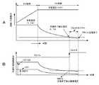
図6Aに示すように、電池電圧が定電圧制御電圧(例えば4.2V)以下の領域では、定電流制御が行われ、一定の充電電流(例えば1.0A)によって定電流充電を行う。充電によって電池電圧(内部起電力)が上昇し、電池電圧Vが4.2Vに達すると、充電装置が定電圧制御の動作に切り換わり、次第に充電電流が減少する。そして、充電電流が設定された充電終了検出値に達したことを検出すると、充電終了が検出される。この時点からフロートタイマーを起動してタイムアウトまで充電して電池への充電を停止する。このような充電動作は、図1に示す充電装置と同様である。 As shown in FIG. 6A, in a region where the battery voltage is equal to or lower than a constant voltage control voltage (for example, 4.2 V), constant current control is performed, and constant current charging is performed with a constant charging current (for example, 1.0 A). When the battery voltage (internal electromotive force) increases due to charging and the battery voltage V reaches 4.2 V, the charging device is switched to the constant voltage control operation, and the charging current gradually decreases. When it is detected that the charging current has reached the set charging end detection value, the charging end is detected. At this point, the float timer is started to charge until timeout and the charging to the battery is stopped. Such a charging operation is the same as that of the charging apparatus shown in FIG.
図6Bは、充電電流検出抵抗R21の両端電圧の変化と、充電電流検出抵抗R21および充電終了検出抵抗R22の直列回路(充電終了検出回路)の両端電圧の変化とを示す。一例として、R21=0.1Ω、R22=0.9Ω、急速充電電流Ic=1.0A、充電終了の電流Is=0.1Aとする。 FIG. 6B shows the change in the voltage across the charging current detection resistor R21 and the change in the voltage across the series circuit (charging termination detection circuit) of the charging current detection resistor R21 and the charging termination detection resistor R22. As an example, it is assumed that R21 = 0.1Ω, R22 = 0.9Ω, rapid charging current Ic = 1.0A, and charging end current Is = 0.1A.
充電電流が1.0A一定の定電流制御の期間では、抵抗R21で(検出電圧V21=Ic×R21=1.0A×0.1Ω=0.1V)の電圧降下が生じる。この0.1VがオペアンプAMP2の+端子に入力される基準電圧と同一電圧となっており、抵抗R21に充電電流1.0Aが流れて、オペアンプAMP2の+端子が降下し、オペアンプAMP2の−端子と同一電位となって、充電電流1.0Aを一定にするように電力制御が行われる。 During a constant current control period in which the charging current is constant at 1.0 A, a voltage drop of (detection voltage V21 = Ic × R21 = 1.0 A × 0.1Ω = 0.1 V) occurs at the resistor R21. This 0.1 V is the same voltage as the reference voltage input to the + terminal of the operational amplifier AMP2, a charging current of 1.0 A flows through the resistor R21, the + terminal of the operational amplifier AMP2 drops, and the-terminal of the operational amplifier AMP2 And the electric power control is performed so that the charging current 1.0A is constant.
また、この時に抵抗R21およびR22の直列回路で生じる電圧降下(検出電圧V2122=Ic×(R21+R22)=1.0A×(0.1+0.9)Ω=1.0V)となる。この電圧は、基準電圧REF2の−端子側に供給されている。抵抗R21とR22の直列抵抗間に生じる検出電圧V2122がコンパレータ6にて基準電圧REF2と比較される。抵抗直列回路は、抵抗R21と比較して抵抗値が大となるので、検出電圧V2122が検出電圧V21より大となる。定電流充電では、コンパレータ6の出力CsがLである。 At this time, a voltage drop (detection voltage V2122 = Ic × (R21 + R22) = 1.0 A × (0.1 + 0.9) Ω = 1.0 V) generated in the series circuit of the resistors R21 and R22. This voltage is supplied to the negative terminal side of the reference voltage REF2. The detection voltage V2122 generated between the series resistors of the resistors R21 and R22 is compared with the reference voltage REF2 by the
定電流充電から定電圧充電に移行すると、充電電流が徐々に減少し、検出電圧V2122が低下する。充電電流が充電終了電流Is=0.1A以下になると、(V2122=0.1A×(0.1+0.9)Ω=0.1V)となる。この電圧と同一電圧がコンパレータ6の+端子側に接続されている基準電圧REF2となる。この場合、コンパレータ6の出力がLからHに変化する。コントローラ11がコントローラ6の出力がLからHに変化したと判断すると、充電終了検出モードの動作に移行する。 When shifting from constant current charging to constant voltage charging, the charging current gradually decreases and the detection voltage V2122 decreases. When the charging current becomes equal to or less than the charging end current Is = 0.1 A, (V2122 = 0.1 A × (0.1 + 0.9) Ω = 0.1 V). The same voltage as this voltage becomes the reference voltage REF2 connected to the + terminal side of the
ここで、図1に示す従来の充電装置において、定電流Icおよび充電終了電流Isを抵抗R2で検出する場合について、上述した条件と同一で検討する。抵抗R2=R21=0.1Ωとし、抵抗R2における電圧降下をV2とする。充電終了時の電流値Is=V2/R2であるので、(V2=Is×R2=0.1A×0.1Ω=0.01V)となる。 Here, in the conventional charging device shown in FIG. 1, the case where the constant current Ic and the charging end current Is are detected by the resistor R2 is examined under the same conditions as described above. Resistance R2 = R21 = 0.1Ω, and voltage drop at resistance R2 is V2. Since the current value Is = V2 / R2 at the end of charging, (V2 = Is × R2 = 0.1 A × 0.1Ω = 0.01 V).
この電圧値は、上述したこの発明の一実施の形態における電圧値V2122=0.1Vと比較すると、1/10の値である。このことは、充電終了検出用の基準電圧REF2を非常に小さく設定することが必要とされ、コンパレータ6として、オフセット電圧の小さい高精度オフセットのコンパレータを使用する必要があり,高価な部品を必要とする。この発明の一実施の形態は、かかる問題を解決することができ、充電終了検出の精度を高くすることができる。 This voltage value is 1/10 of the voltage value V2122 = 0.1 V in the embodiment of the present invention described above. This means that it is necessary to set the reference voltage REF2 for detecting the end of charging very small, and it is necessary to use a high-precision offset comparator with a small offset voltage as the
さらに、この発明の一実施の形態では、ショットキーダイオードD5を抵抗R22と並列に接続しているので、抵抗R22における電力損失を低減することができる。図6Bに示す検出電圧V2122は、ショットキーダイオードD5を接続していない場合のものであり、定電流制御時にV2122=0.9Vである。ショットキーダイオードD5の順方向電圧降下Vfは、例えば0.4Vであり、図7に示すように、ショットキーダイオードD5によって検出電圧V2122が0.4V以下に抑えられる。その結果、抵抗R22における損失を1/2以下へ減少させることができる。なお、ショットキーダイオード以外のダイオードを使用しても良いが、順方向電圧降下がなるべく小さいことが損失を抑える点で好ましい。 Furthermore, in the embodiment of the present invention, since the Schottky diode D5 is connected in parallel with the resistor R22, power loss in the resistor R22 can be reduced. The detection voltage V2122 shown in FIG. 6B is obtained when the Schottky diode D5 is not connected, and is V2122 = 0.9 V during constant current control. The forward voltage drop Vf of the Schottky diode D5 is, for example, 0.4V, and the detection voltage V2122 is suppressed to 0.4V or less by the Schottky diode D5 as shown in FIG. As a result, the loss in the resistor R22 can be reduced to ½ or less. Although a diode other than a Schottky diode may be used, it is preferable that the forward voltage drop is as small as possible in terms of suppressing loss.
上述したこの発明の一実施の形態は、下記の効果を奏する。
1)定電流制御のための電流検出抵抗R21に対して直列に抵抗R22を接続し、この直列回路の抵抗(R21+R22)に発生する電圧をコンパレータにおいて基準電圧REF2と比較するので、充電終了時の検出値を大きくすることが可能となり、通常のオフセットのコンパレータを使用することができ、基準電圧REF2の設定も容易となる。
2)定電圧制御の電流は、抵抗R21の抵抗値によって設定することができ、充電終了検出の電流値も直列に接続する抵抗R22の抵抗値によって設定することができ、内部の基準電圧の値を変更することなく、電流設定の自由度が拡大し、回路設計が容易となる利点がある。
3)充電終了用に直列に追加する抵抗R22と並列にダイオードD5を接続することによって、抵抗R22に発生する電圧がダイオードの順方向電圧降下以上になった場合に、ダイオードを介して電流をバイパスすることによって、抵抗R22で発生する損失を抑えることができる。充電電流が比較的大きい場合には、抵抗R22で発生する損失を低減することによる利点が大きい。One embodiment of the present invention described above has the following effects.
1) A resistor R22 is connected in series to the current detection resistor R21 for constant current control, and the voltage generated in the resistor (R21 + R22) of this series circuit is compared with the reference voltage REF2 in the comparator. The detection value can be increased, a normal offset comparator can be used, and the reference voltage REF2 can be easily set.
2) The current of the constant voltage control can be set by the resistance value of the resistor R21, the current value of the end of charge detection can also be set by the resistance value of the resistor R22 connected in series, and the value of the internal reference voltage There is an advantage that the degree of freedom of current setting is expanded and the circuit design is facilitated without changing.
3) By connecting the diode D5 in parallel with the resistor R22 added in series for the end of charging, when the voltage generated at the resistor R22 exceeds the forward voltage drop of the diode, the current is bypassed through the diode. By doing so, the loss which generate | occur | produces by resistance R22 can be suppressed. When the charging current is relatively large, the advantage of reducing the loss generated in the resistor R22 is great.
以上、この発明の一実施形態について説明したが、この発明は、一実施形態に限定されるものではなく、この発明の要旨を逸脱しない範囲内で様々な変形や応用が可能である。例えば複数本の2次電池を充電しても良く、充電電圧および充電電流を出力する電源回路としては、一実施の形態に示される構成以外のものを使用しても良い。 As mentioned above, although one Embodiment of this invention was described, this invention is not limited to one Embodiment, A various deformation | transformation and application are possible within the range which does not deviate from the summary of this invention. For example, a plurality of secondary batteries may be charged, and a power supply circuit that outputs a charging voltage and a charging current other than the configuration shown in the embodiment may be used.
2 整流回路
3 パルス幅変調制御回路
4 スイッチ部
5a +側電源出力端子
5b −側電源入力端子
6 コンパレータ
11 コントローラ
BAT 2次電池
AMP1,AMP2 オペアンプ
R21 充電電流検出抵抗
R22 充電終了検出抵抗
D5 ショットキーダイオード2
Claims (5)
Translated fromJapanese定電流制御検出用第1の抵抗と、充電終了を検出する充電終了検出用第2の抵抗とが直列に充電電流の電流路に挿入され、
上記第1の抵抗に発生する第1の検出電圧によって定電流制御を行い、
上記第1の抵抗および上記第2の抵抗の直列抵抗に発生する第2の検出電圧をコンパレータにて基準電圧と比較し、上記第2の検出電圧が上記基準電圧より小となることを充電終了として検出し、
上記第2の抵抗と並列に充電電流に対して順方向のダイオードが接続され、
上記第2の抵抗に発生する電圧が上記ダイオードの順方向電圧降下以上になった場合に、上記充電電流を上記ダイオードによってバイパスすることによって、上記第2の抵抗の損失を低減した充電装置。A charging device in which a secondary battery is charged by a power supply circuit that converts AC input into DC output, and the output characteristics of the power supply circuit are constant current control and constant voltage control characteristics,
The first resistor for constant current control detection and the second resistor for charge end detection for detecting the end of charge are inserted in series in the current path of the charge current,
Constant current control is performed by the first detection voltage generated in the first resistor,
The second detection voltage generated in the series resistance of the first resistor and the second resistor is compared with a reference voltage by a comparator, and charging ends when the second detection voltage becomes smaller than the reference voltage. detectedas,
A forward diode is connected to the charging current in parallel with the second resistor,
A charging devicein which a loss of the second resistor is reduced by bypassing the charging current by the diode when a voltage generated in the second resistor becomes equal to or higher than a forward voltage drop of the diode .
上記パルス幅変調制御回路と上記第1および第2の抵抗の間がトランスによって絶縁され、
上記第1の検出電圧がホトカプラを介して上記パルス幅変調制御回路に供給される請求項1記載の充電装置。A pulse width modulation control circuit for power control of the power supply circuit;
The pulse width modulation control circuit and the first and second resistors are insulated by a transformer,
The charging device according to claim 1, wherein the first detection voltage is supplied to the pulse width modulation control circuit via a photocoupler.
Priority Applications (4)
| Application Number | Priority Date | Filing Date | Title |
|---|---|---|---|
| JP2007193326AJP4380747B2 (en) | 2007-07-25 | 2007-07-25 | Charger |
| TW097121433ATWI392194B (en) | 2007-07-25 | 2008-06-09 | Battery charger |
| US12/176,448US8098052B2 (en) | 2007-07-25 | 2008-07-21 | Battery charger |
| CN2008101350187ACN101355263B (en) | 2007-07-25 | 2008-07-24 | Battery charger |
Applications Claiming Priority (1)
| Application Number | Priority Date | Filing Date | Title |
|---|---|---|---|
| JP2007193326AJP4380747B2 (en) | 2007-07-25 | 2007-07-25 | Charger |
Publications (2)
| Publication Number | Publication Date |
|---|---|
| JP2009033824A JP2009033824A (en) | 2009-02-12 |
| JP4380747B2true JP4380747B2 (en) | 2009-12-09 |
Family
ID=40294707
Family Applications (1)
| Application Number | Title | Priority Date | Filing Date |
|---|---|---|---|
| JP2007193326AExpired - Fee RelatedJP4380747B2 (en) | 2007-07-25 | 2007-07-25 | Charger |
Country Status (4)
| Country | Link |
|---|---|
| US (1) | US8098052B2 (en) |
| JP (1) | JP4380747B2 (en) |
| CN (1) | CN101355263B (en) |
| TW (1) | TWI392194B (en) |
Families Citing this family (11)
| Publication number | Priority date | Publication date | Assignee | Title |
|---|---|---|---|---|
| JP4817054B2 (en)* | 2006-03-02 | 2011-11-16 | 日立工機株式会社 | Charger |
| US8159204B2 (en)* | 2008-09-29 | 2012-04-17 | Active-Semi, Inc. | Regulating current output from a buck converter without external current sensing |
| JP4770916B2 (en)* | 2008-11-17 | 2011-09-14 | 日本テキサス・インスツルメンツ株式会社 | Electronic price tag system |
| WO2010073593A1 (en)* | 2008-12-22 | 2010-07-01 | 新電元工業株式会社 | Battery charger |
| CN101702528B (en)* | 2009-11-19 | 2014-10-29 | 北京中星微电子有限公司 | Battery charging control device |
| KR101113415B1 (en)* | 2009-12-29 | 2012-03-02 | 삼성에스디아이 주식회사 | Protection Circuit for Battery Pack |
| CN104600820B (en)* | 2014-12-30 | 2017-01-18 | 上海力申科学仪器有限公司 | Lead-acid cell quick charge control circuit |
| CN105305551B (en)* | 2015-11-11 | 2018-11-30 | 南京矽力杰半导体技术有限公司 | Charge power supply and its control method |
| US9997945B2 (en)* | 2015-11-30 | 2018-06-12 | Oura Health Oy | Chargeable device and charger thereof |
| EP3282550B1 (en)* | 2016-02-05 | 2020-04-15 | Guangdong Oppo Mobile Telecommunications Corp., Ltd. | Adapter and charging control method |
| CN112018844B (en)* | 2020-08-24 | 2022-04-22 | 维沃移动通信有限公司 | Charging parameter detection circuit, method and charger |
Family Cites Families (10)
| Publication number | Priority date | Publication date | Assignee | Title |
|---|---|---|---|---|
| JP3430264B2 (en)* | 1992-06-23 | 2003-07-28 | ソニー株式会社 | Charging device |
| JP2601974B2 (en)* | 1992-09-16 | 1997-04-23 | インターナショナル・ビジネス・マシーンズ・コーポレイション | Power supply for electronic equipment and electronic equipment system |
| JP3735999B2 (en)* | 1997-02-20 | 2006-01-18 | ソニー株式会社 | Charger |
| JP3157127B2 (en)* | 1997-08-07 | 2001-04-16 | セイコーインスツルメンツ株式会社 | Charge / discharge control circuit with charge / discharge current detection function and rechargeable power supply |
| JP4453172B2 (en)* | 2000-07-28 | 2010-04-21 | ソニー株式会社 | Power supply device and power supply system |
| CN1564421A (en)* | 2004-03-17 | 2005-01-12 | 毛锦铭 | Charger for lithium cell |
| TWI364600B (en)* | 2004-04-12 | 2012-05-21 | Kuraray Co | An illumination device an image display device using the illumination device and a light diffusing board used by the devices |
| JP2006121797A (en)* | 2004-10-20 | 2006-05-11 | Matsushita Electric Ind Co Ltd | Charger |
| JP4526453B2 (en)* | 2005-07-07 | 2010-08-18 | パナソニック株式会社 | Charger |
| JP5029055B2 (en)* | 2007-02-16 | 2012-09-19 | 富士通セミコンダクター株式会社 | Detection circuit and power supply system |
- 2007
- 2007-07-25JPJP2007193326Apatent/JP4380747B2/ennot_activeExpired - Fee Related
- 2008
- 2008-06-09TWTW097121433Apatent/TWI392194B/ennot_activeIP Right Cessation
- 2008-07-21USUS12/176,448patent/US8098052B2/ennot_activeExpired - Fee Related
- 2008-07-24CNCN2008101350187Apatent/CN101355263B/ennot_activeExpired - Fee Related
Also Published As
| Publication number | Publication date |
|---|---|
| US8098052B2 (en) | 2012-01-17 |
| TWI392194B (en) | 2013-04-01 |
| TW200908508A (en) | 2009-02-16 |
| JP2009033824A (en) | 2009-02-12 |
| CN101355263B (en) | 2011-05-11 |
| US20090027011A1 (en) | 2009-01-29 |
| CN101355263A (en) | 2009-01-28 |
Similar Documents
| Publication | Publication Date | Title |
|---|---|---|
| JP4380747B2 (en) | Charger | |
| JP4479760B2 (en) | Charging apparatus and charging method | |
| RU2448402C2 (en) | Device for charging batteries | |
| JP4766095B2 (en) | Charger | |
| JP4333777B2 (en) | Charger | |
| US11146094B2 (en) | Electrical apparatus | |
| US20110025255A1 (en) | Solar Power System For Charging Battery Pack | |
| JP6641665B2 (en) | Power storage state adjustment device, battery pack, load system, and power storage state adjustment method | |
| JP4526453B2 (en) | Charger | |
| JP2012055043A (en) | Charging system, battery pack, and charger | |
| JP2020043763A (en) | Power storage state adjustment device, battery pack, load system, and power storage state adjustment method | |
| JP2006158103A (en) | Charger | |
| JP3019353B2 (en) | Charging device | |
| JP4962547B2 (en) | Power supply apparatus and power supply method | |
| JP4407157B2 (en) | Power supply device and power supply method | |
| JP4046139B2 (en) | Battery charger | |
| JPH09147921A (en) | Charging method for secondary battery | |
| JP5419551B2 (en) | Charging device and lighting device | |
| JPH04248333A (en) | Charger | |
| JP4060103B2 (en) | Electronic equipment power supply circuit | |
| JP2020145771A (en) | Charge/discharge controller and storage battery with charge/discharge controller | |
| JPH1070847A (en) | Charger | |
| JP2000181550A (en) | Charger and power supply |
Legal Events
| Date | Code | Title | Description |
|---|---|---|---|
| A977 | Report on retrieval | Free format text:JAPANESE INTERMEDIATE CODE: A971007 Effective date:20090611 | |
| A131 | Notification of reasons for refusal | Free format text:JAPANESE INTERMEDIATE CODE: A131 Effective date:20090630 | |
| A521 | Request for written amendment filed | Free format text:JAPANESE INTERMEDIATE CODE: A523 Effective date:20090810 | |
| TRDD | Decision of grant or rejection written | ||
| A01 | Written decision to grant a patent or to grant a registration (utility model) | Free format text:JAPANESE INTERMEDIATE CODE: A01 Effective date:20090901 | |
| A01 | Written decision to grant a patent or to grant a registration (utility model) | Free format text:JAPANESE INTERMEDIATE CODE: A01 | |
| A61 | First payment of annual fees (during grant procedure) | Free format text:JAPANESE INTERMEDIATE CODE: A61 Effective date:20090914 | |
| FPAY | Renewal fee payment (event date is renewal date of database) | Free format text:PAYMENT UNTIL: 20121002 Year of fee payment:3 | |
| R151 | Written notification of patent or utility model registration | Ref document number:4380747 Country of ref document:JP Free format text:JAPANESE INTERMEDIATE CODE: R151 | |
| FPAY | Renewal fee payment (event date is renewal date of database) | Free format text:PAYMENT UNTIL: 20121002 Year of fee payment:3 | |
| FPAY | Renewal fee payment (event date is renewal date of database) | Free format text:PAYMENT UNTIL: 20131002 Year of fee payment:4 | |
| R250 | Receipt of annual fees | Free format text:JAPANESE INTERMEDIATE CODE: R250 | |
| R250 | Receipt of annual fees | Free format text:JAPANESE INTERMEDIATE CODE: R250 | |
| R250 | Receipt of annual fees | Free format text:JAPANESE INTERMEDIATE CODE: R250 | |
| R250 | Receipt of annual fees | Free format text:JAPANESE INTERMEDIATE CODE: R250 | |
| R250 | Receipt of annual fees | Free format text:JAPANESE INTERMEDIATE CODE: R250 | |
| R250 | Receipt of annual fees | Free format text:JAPANESE INTERMEDIATE CODE: R250 | |
| R250 | Receipt of annual fees | Free format text:JAPANESE INTERMEDIATE CODE: R250 | |
| R250 | Receipt of annual fees | Free format text:JAPANESE INTERMEDIATE CODE: R250 | |
| R250 | Receipt of annual fees | Free format text:JAPANESE INTERMEDIATE CODE: R250 | |
| LAPS | Cancellation because of no payment of annual fees |