JP4378847B2 - Equipment that uses electronic devices - Google Patents
Equipment that uses electronic devicesDownload PDFInfo
- Publication number
- JP4378847B2 JP4378847B2JP2000157098AJP2000157098AJP4378847B2JP 4378847 B2JP4378847 B2JP 4378847B2JP 2000157098 AJP2000157098 AJP 2000157098AJP 2000157098 AJP2000157098 AJP 2000157098AJP 4378847 B2JP4378847 B2JP 4378847B2
- Authority
- JP
- Japan
- Prior art keywords
- electronic device
- function
- current
- register
- current value
- Prior art date
- Legal status (The legal status is an assumption and is not a legal conclusion. Google has not performed a legal analysis and makes no representation as to the accuracy of the status listed.)
- Expired - Fee Related
Links
Images


Classifications
- G—PHYSICS
- G06—COMPUTING OR CALCULATING; COUNTING
- G06F—ELECTRIC DIGITAL DATA PROCESSING
- G06F1/00—Details not covered by groups G06F3/00 - G06F13/00 and G06F21/00
- G06F1/26—Power supply means, e.g. regulation thereof
- G06F1/266—Arrangements to supply power to external peripherals either directly from the computer or under computer control, e.g. supply of power through the communication port, computer controlled power-strips
Landscapes
- Engineering & Computer Science (AREA)
- General Engineering & Computer Science (AREA)
- Theoretical Computer Science (AREA)
- Computer Hardware Design (AREA)
- Physics & Mathematics (AREA)
- General Physics & Mathematics (AREA)
- Power Sources (AREA)
Description
Translated fromJapanese【0001】
本発明は、例えば本体機器に対して着脱自在に設けられて任意の機能を行う機器に使用して好適な電子装置を使用する機器に関する。詳しくはメモリカード装置、あるいはそれに類似する半導体メモリ装置と同等の形状を有し、これらの装置の接続部に接続されて任意の機能を実行する電子装置を使用する機器に関するものである。
【0002】
【従来の技術】
例えば本体機器に対して着脱自在に設けられるメモリカード装置、あるいはそれに類似する半導体メモリ装置と同等の形状を有し、本体機器のこれらのメモリ装置等の接続部に接続されて任意の機能を実行する電子装置が提案されている。すなわちこのような電子装置においては、例えばコンピュータネットワークへの接続機能や外部との通信機能を持たせることによって、本体機器の運用や用途を容易に拡張することができるようになるものである。
【0003】
【発明が解決しようとする課題】
ところがこのような電子装置において、電子装置に設けられる機能によって、その機能が実行された場合の消費電流が大幅に変化する。すなわち例えば上述のコンピュータネットワークへの接続機能や外部との通信機能を実行する場合には、従来のメモリ機能のみの場合に比べて数倍の消費電流が必要とされるものである。そこで例えばこのような大きな消費電流の必要とされる電子装置が、従来のメモリ機能のみを想定した本体機器に装着されると、過大な電流が流されて内蔵電池が短時間で消耗されたり、電源電圧が低下されて機能が実行できなくなったり、最悪の場合には本体機器の破損の恐れなども生じるものである。
【0004】
このため従来の装置では、例えば電子装置と本体機器との接続部の形状を、メモリ機能のみの場合と大きな消費電流を必要とされる場合とで違えて、消費電流の異なる電子装置が装着されないようにすることが行われている。しかしながらこのような対策では、接続部の形状を違えるための構造の形成が容易ではなく、また将来より大きな消費電力の電子装置が形成された場合には、さらに形状を違えた構造が必要になるなど、抜本的な解決にはならないものである。
【0005】
この出願はこのような点に鑑みて成されたものであって、解決しようとする問題点は、従来の装置では、消費電流の異なる電子装置を本体機器に装着して使用する場合に、過大な電流の発生によって内蔵電池が短時間で消耗されたり、電源電圧の低下によって機能が実行できなくなったり、最悪の場合には本体機器の破損なども生じる恐れがあり、また消費電流に応じて接続部の形状を違えるような対策では抜本的な解決にはならなかったというものである。
【0006】
【課題を解決するための手段】
このため本発明においては、メモリ機能及び拡張機能を有し、使用する機能の組み合わせによって内部で消費される電流値を所定のアドレスのエリアに記載したレジスタが設けられた電子装置と、メモリ機能のみを有し、前記エリアに内部で消費される電流値が記載されていないレジスタが設けられた電子装置とのいずれもが着脱自在に設けられ、装着された電子装置との間で任意のデータの交換を行うと共に、装着された電子装置の機能を実行させる電子装置を使用する機器であって、
装着された電子装置に設けられたレジスタの前記エリアから電流値を読み出す手段と、
前記エリアから読み出された電流値が、当該機器の仕様通りであるか、または前記仕様通りではないが供給可能であり且つ0でない場合は、読み出された電流値に従った駆動電流を前記電子装置に供給し、前記エリアから読み出された電流値が、前記仕様通りでなく且つ供給不可能であるか、または0である場合は、前記仕様通りの電流値に従った駆動電流を前記電子装置に供給する手段とを有してなるものである。
【0007】
【発明の実施の形態】
以下、図面を参照して本発明を説明するに、
1243313796828_0
は本発明を適用した一の実施形態である電子装置と、他の実施形態である電子装置を使用する機器の構成を示すブロック図である。
【0010】
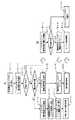
図1において、図面の左側は電子装置を使用する機器としての本体機器100を示す。この本体機器100には、メインメモリ(図示せず)等に記憶されたデータファイルを入出力するファイルマネージャー10が設けられ、このファイルマネージャー10のデータがメモリ用の通信プロトコル回路11を通じてシリアルインターフェース12と交換される。また、任意の拡張機能を実行するためのドライバー13が設けられ、このドライバー13のデータが拡張機能用の通信プロトコル回路14を通じてシリアルインターフェース12と交換される。
【0011】
さらにこのシリアルインターフェース12の入出力端子が接続部のそれぞれ所定の接点に接続される。また、電源装置15からの電源VCC及びVSSが接続部のそれぞれ所定の接点に接続される。すなわちこの接続部には、例えば10個の接点101〜110が設けられる。そしてこの内の接点101には電源VSSが接続される。また接点102には電源VCCが接続される。さらに接点103にはシリアルインターフェース12からのシリアルデータクロック(SCLK)が接続される。
【0012】
また、接点104にはシリアルインターフェース12の拡張機能用のシリアルデータ入出力(SDIO)が接続される。さらに接点105には電子装置の装着の有無を検出する端子INSが接続される。また接点106は未使用である。さらに接点107にはシリアルインターフェース12のメモリ機能用のシリアルデータ入出力(SDIO)が接続される。また接点108には電源VCCが接続される。さらに接点109にはシリアルインターフェース12のバスステイタス出力(BS)が接続される。また接点110には電源VSSが接続される。
【0013】
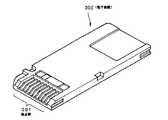
一方、図面の右側は電子装置200を示す。この電子装置200は、例えば図2に示すようにいわゆるメモリカード装置、あるいはそれに類似する半導体メモリ装置と同等の形状を有している。そしてこの電子装置200が本体機器100に対して着脱自在に設けられると共に、その端部に形成される接点群201を介して、上述の本体機器100の接点101〜110に電気的に接続されるものである。これによって、本体機器100と電子装置200との間での電源の供給及びデータの交換が行われる。
【0014】
すなわち図1においては、電子装置200に設けられるシリアルインターフェース20と本体機器100に設けられるシリアルインターフェース12との間でデータの交換が行われる。さらにこのシリアルインターフェース20とレジスタ21及びページバッファ22との間でデータの交換が行われる。そしてこのページバッファ22に拡張機能のインターフェース23が接続されて、例えばコンピュータネットワーク(LAN:Local Area Netwotk)への接続機能や外部との通信機能を実行するためのデータの交換が行われる。
【0015】
また、上述のページバッファ22にはメモリ機能のインターフェース24が接続されて、例えばフラッシュメモリ25の書き込み及び読み出しを行うためのデータの交換が行われる。なおページバッファ22の一部には、フラッシュメモリ25に書き込まれるデータに誤り検出コード(ECC)を付加するためのECC回路22eが設けられる。そしてこのECC回路22eで発生された誤り検出コードがインターフェース24に供給されて、上述のデータと共にフラッシュメモリ25に書き込まれる。
【0016】
さらに電子装置200には、属性メモリ(ROM)26が設けられる。この属性メモリ26には電子装置200のヴァージョン番号や初期設定値が記憶されているものである。そしてこの電子装置200が本体機器100の装着されると、最初にこの属性メモリ26のヴァージョン番号が本体機器100に読み出され、この本体機器100からのヴァージョン番号に従ったコマンドによって電子装置200の初期設定が行われる。この初期設定によって、例えばレジスタ21の所定のエリアに、電子装置200の内部で消費される電流値が記載される。
【0017】
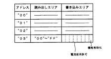
ここでレジスタ21には、例えば図3に示すように複数のアドレスが設けられ、各アドレスは例えば8ビットずつの読み出しエリアと書き込みエリアで構成される。そして例えばアドレス“03”(“−−”は16進値を示す)の読み出しエリアが電流値の記載エリアとされ、例えば“00”〜“FF”の値で電流値が記載される。また、同じアドレス“03”の書き込みエリアは制御信号の記載エリアとされ、例えば第4ビットが電流使用許可ビット(1:使用可、0:使用不可)とされ、第8ビットが機能有効化ビット(1:機能有効、0:機能無効)とされる。なお、他のアドレスには初期値等が記載される。
【0018】
また、電子装置200には振動子27が設けられ、この振動子27からの信号が発振器28に供給されて内部の動作クロック信号が発生される。そしてこのクロック信号が電子装置200内の各回路に供給される。さらにスイッチ29はフラッシュメモリ25に書き込まれたデータが誤って書き換えられるのを防ぐためのもので、例えば図示のように電源VCC側に接続されているときはデータの書き込みが許可され、逆に接地側に接続されているときは書き込みが禁止されて、誤ってデータが書き換えられるのを防ぐことができる。
【0019】
さらに上述の本体機器100で電源VCCが接続される接点102、108に対応する電子装置200側の接点は互いに接続されて電子装置200の電源部とされる。すなわちこれらの接点102、108に対応する接点の接続中点が、電子装置200の各回路の電源VCCに接続される。ただし、例えば拡張機能のインターフェース23とメモリ機能のインターフェース24には、それぞれ電源制御回路23pと24pを通じて電源VCCが接続され、これらの制御回路23pと24pがレジスタ21に記入される値に従って制御される。
【0020】
また、上述の本体機器100で電源VSSが接続される接点101、110に対応する電子装置200側の接点は互いに接続されて電子装置200の接地部とされると共に、この接地部に接点105に対応する接点が接続される。これによって、例えば本体機器100で接点105に任意の電位を与えておくことにより電子装置200が装着されると接点105の電位が接地電位となり、この電位の変化を検出することで本体機器100側で電子装置200の装着の有無を検出することができる。
【0021】
そしてこのような本体機器100及び電子装置200に対して、図4は電子装置200が単機能の場合に、機能が開始されるまでの処理の流れを示す。なお図4のAは本体機器100側の処理を示し、Bは電子装置200側の処理を示している。この図4のAにおいて、ステップ〔A1〕で電子装置200のレジスタ21に記載された電流値が読み出される。次にステップ〔A2〕でこの電流値が本体機器100の仕様通りか否か判断され、仕様通りでないと判断されたとき(No)はさらにステップ〔A3〕で電流供給が可能か否か判断される。
【0022】
さらにステップ〔A3〕で電流供給が不可と判断されたとき(No)は、ステップ〔A4〕で電子装置200のレジスタ21のアドレス“03”の第4ビットに電流使用不可(0)を記入し、ステップ〔A5〕で電子装置200が使用できないことを使用者に告知する。またステップ〔A3〕で電流供給が可能と判断されたとき(Yes)、及びステップ〔A2〕で仕様通りであると判断されたとき(Yes)は、ステップ〔A6〕で電子装置200のレジスタ21のアドレス“03”の第4ビットに電流使用可(1)を記入する。
【0023】
これに対して図4のBにおいては、ステップ〔B1〕でレジスタ21のアドレス“03”の第4ビットが読み出される。さらにステップ〔B2〕でこの第4ビットの値に応じて電流供給が可能か否か判断される。すなわち第4ビットが値(1)のときは電流供給が可能と判断され、第4ビットが値(0)のときは電流供給が不可と判断される。そしてステップ〔B2〕で電流供給が不可と判断されたとき(No)は、ステップ〔B3〕でレジスタ21のアドレス“03”の第8ビットに機能無効(0)のままにされ、電子装置200は不動作にされる。
【0024】
一方、ステップ〔B2〕で電流供給が可能と判断されたとき(Yes)は、ステップ〔B4〕でレジスタ21のアドレス“03”の第8ビットに機能有効(1)が記入される。さらに図4のAのステップ〔A7〕でレジスタ21の第8ビットが機能有効(1)になったことが確認されると、ステップ〔A8〕でステップ〔A1〕で読み出された電流値に従った要求電流が、電源VCCの接続される接点102、108及び電源VSSの接続される接点101、110に供給される。そして図4のBのステップ〔B5〕で電子装置200の動作が開始される。
【0025】
すなわちレジスタ21のアドレス“03”には、最初に例えば図5のAに示すように読み出しエリアに電子装置200で要求される電流値が16進値で記載される。なお、図示の値は“41”=65mAである。これに対してこの電流値が本体機器100から供給可能であるときは、図5のBに示すように書き込みエリアの第4ビットの電流使用許可ビットが(1)にされる。さらに電子装置200で電流使用許可ビットが確認されて機能が有効にされると、図5のCに示すように書き込みエリアの第8ビットの機能有効化ビットが(1)にされる。
【0026】
このようにして、電子装置200で要求される電流値が本体機器100で確認され、この電流値が本体機器100から供給可能であるときは電子装置200で機能が動作されると共に、電流値が本体機器100から供給できないときは、電子装置200の機能が動作されないようにすることができる。これによって、過大な電流が流されて本体機器100の内蔵電池が短時間で消耗されたり、電源電圧が低下されて機能が実行できなくなったり、最悪の場合には本体機器100の破損するなどの恐れを解消することができるものである。
【0027】
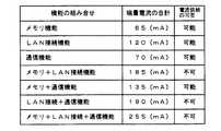
さらに上述の実施形態において、電子装置200には複数の機能が設けられている場合には、それらの機能の組み合わせによって要求される消費電流が異なる場合がある。すなわち図6において、例えばメモリ機能とLAN接続機能、及び通信機能が設けられている場合に、それぞれの機能を単独で使用した場合の消費電流はそれぞれ異なるものであり、さらにそれらの機能の組み合わせて使用した場合の消費電流もそれぞれ組み合わせごとに異なり、例えば3つの機能が設けられている場合には7通りの消費電流が要求されることになる。
【0028】
従ってこのような場合には、機能の組み合わせによって電流供給ができる場合と、できない場合とが生じることがある。すなわち例えば図6に示すように、メモリ機能の消費電流を65mA、LAN接続機能の消費電流を120mA、通信機能の消費電流を70mAとした場合に、それぞれ組み合わせの消費電流は図中に示すようになる。これに対して、本体機器100から供給可能な電流の最大値を例えば150mAとすると、各機能の単独の場合とメモリ機能と通信機能の組み合わせでは電流供給が可能であるが、他の組み合わせは不可となる。
【0029】
そこで図7には、電子装置200が複数の機能を有している場合の、機能が開始されるまでの処理の流れを示す。なお図7のAは本体機器100側の処理を示し、Bは電子装置200側の処理を示している。そしてこの図7のAにおいて、ステップ〔A11〕で拡張機能用のレジスタへの切り換えが行われる。次に、ステップ〔A12〕で電子装置200のレジスタ21に記載された電流値が読み出される。さらにステップ〔A13〕でこの電流値が本体機器100の仕様通りか否か判断される。
【0030】
そしてステップ〔A13〕で電流値が仕様通りでないと判断されたとき(No)は、さらにステップ〔A14〕で電流供給が可能か否か判断され、電流供給が不可と判断されたとき(No)は、ステップ〔A15〕で電子装置200のレジスタ21のアドレス“03”の第4ビットに電流使用不可(0)が記入される。さらにステップ〔A16〕で電子装置200の拡張機能が使用できないことが使用者に告知され、ステップ〔A17〕で電子装置200をメモリ機能のみとするように本体機器100側の切り替えが行われる。
【0031】
またステップ〔A14〕で電流供給が可能と判断されたとき(Yes)と、ステップ〔A13〕で仕様通りであると判断されたとき(Yes)は、ステップ〔A18〕で電子装置200のレジスタ21のアドレス“03”の第4ビットに電流使用可(1)が記入される。このレジスタ21のアドレス“03”の第4ビットが図7のBのステップ〔B11〕で読み出される。そしてステップ〔B12〕でこの第4ビットの値に応じて電流供給が可能か否か判断される。すなわち第4ビットが値(1)のときは可能、値(0)のときは不可と判断される。
【0032】
そしてステップ〔B12〕で電流供給が可能と判断されたとき(Yes)は、ステップ〔B13〕でレジスタ21のアドレス“03”の第8ビットに機能有効(1)が記入される。さらに図7のAのステップ〔A19〕でレジスタ21の第8ビットが機能有効(1)になったことが確認されると、ステップ〔A20〕でステップ〔A12〕で読み出された電流値に従った要求電流が、接点102、108及び接点101、110に供給される。そして図7のBのステップ〔B14〕で電子装置200の動作が開始される。
【0033】
さらに図7のAのステップ〔A14〕で電流供給が不可と判断されたとき(No)の処理では、ステップ〔A21〕で仕様通りの電流が接点102、108及び接点101、110供給される。そして図7のBのステップ〔B12〕で電流供給が不可と判断されたとき(No)の処理では、レジスタ21のアドレス“03”の第8ビットに機能無効(0)のままにされ、ステップ〔B15〕で電子装置200のメモリ機能のみが動作される。これによって本体機器100側で電流供給が不可のときは、電子装置200のメモリ機能のみが動作される。
【0034】
このようにして、電子装置200で要求される電流値が本体機器100で確認され、この電流値が本体機器100から供給可能であるときは電子装置200で機能が動作されると共に、電流値が本体機器100から供給できないときは、電子装置200の供給可能な機能のみが動作されるようにすることができる。これによって、過大な電流が流されて本体機器100の内蔵電池が短時間で消耗されたり、電源電圧が低下されて機能が実行できなくなったり、最悪の場合には本体機器100の破損するなどの恐れを解消することができるものである。
【0035】
従ってこの実施形態において、電子装置に必要な消費電流値を記載したレジスタを設け、このレジスタの値を本体機器が読み出して、それに応じた電流を電子装置に供給することによって、電子装置には常に必要な消費電流が供給されて、電子装置に設けられた所望の機能を円滑に実行することができると共に、消費電流がさらに増加するような場合にも良好に対応することができる。
【0036】
これによって、従来の装置では、消費電流の異なる電子装置を本体機器に装着して使用する場合に、過大な電流の発生によって内蔵電池が短時間で消耗されたり、電源電圧の低下によって機能が実行できなくなったり、最悪の場合には本体機器の破損なども生じる恐れがあり、また消費電流に応じて接続部の形状を違えるような対策では抜本的な解決にはならなかったものを、本発明によればこれらの問題点を容易に解消することができるものである。
【0037】
なお上述の実施形態において、例えばレジスタ21のアドレス“03”の読み出しエリアに、例えば値“00”=0mAのように消費電流値としてはあり得ない値が記載されていた場合には、その値を供給電流値とはせずに、仕様通りの電流供給が行われるようにする。これによって、例えば従来仕様のレジスタ21にアドレス“03”を持たない電子装置が装着された場合には、仕様通りの電流供給が行われて、例えば従来仕様の電子装置をそのまま使用することができ、従来仕様の電子装置との互換性を持たせることができる。
【0038】
また上述の実施形態において、例えば接点104は拡張機能用のシリアルデータ入出力(SDIO)に用いられるが、この接点104は従来仕様のメモリ機能のみの電子装置では未使用になっている。その場合に、この接点104を任意の機能が有効とされるまでは高インピーダンスに保ち、その機能が有効になってときのみ導通されることによって、例えば従来仕様のメモリ機能のみの電子装置を対象とした本体機器にこの電子装置が装着されても、不要な電流が流れることの無いようにすることができる。
【0039】
さらに本発明は、上述の説明した実施の形態に限定されるものではなく、本発明の精神を逸脱することなく種々の変形が可能とされるものである。
【0040】
【発明の効果】
従って請求項1の発明の電子装置を使用する機器によれば、装着された電子装置に設けられたレジスタの所定のアドレスのエリアから電子装置の内部で消費される電流値を読み出して、それに応じた電流を電子装置に供給することによって、従来の機器では、メモリ機能及び拡張機能を有する電子装置を本体機器に装着して使用する場合に、過大な電流の発生によって内蔵電池が短時間で消耗されたり、電源電圧の低下によって機能が実行できなくなったり、最悪の場合には本体機器の破損なども生じる恐れがあり、また消費電流に応じて接続部の形状を違えるような対策では抜本的な解決にはならなかったものを、本発明によればこれらの問題点を容易に解消することができるものである。
また、レジスタの所定のアドレスのエリアに内部で消費される電流値が記載されていない従来仕様のメモリ機能のみを有する電子装置が装着された場合には、仕様通りの電流供給が行われて、従来仕様の電子装置をそのまま使用することができ、従来仕様の電子装置との互換性を持たせることができるものである。
【0044】
さらに請求項2の発明によれば、駆動電流の供給の可否を示す情報を、メモリ機能及び拡張機能を有する電子装置のレジスタの所定のアドレスのエリアに記入する手段を有することによって、駆動電流の供給を円滑に行うことができるものである。
【0045】
さらに請求項3の発明によれば、駆動電流の供給の可否に従ってメモリ機能及び拡張機能を有する電子装置で実行される機能の有効無効を示す情報を、レジスタの所定のアドレスのエリアから読み出す手段を有することによって、機能の実行を円滑に行うことができるものである。
【図面の簡単な説明】
【図1】本発明の適用される電子装置及び本体機器の一実施形態の構成図である。
【図2】本発明の適用される電子装置の一実施形態の外観図である。
【図3】その説明のための線図である。
【図4】その動作の説明のための一の流れ図である。
【図5】その説明のための線図である。
【図6】その説明のための線図である。
【図7】その動作の説明のための他の流れ図である。
【符号の説明】
100…本体機器、10…ファイルマネージャー、11…メモリ機能のプロトコル回路、12…シリアルインターフェース、13…任意の拡張機能を実行するためのドライバー、14…拡張機能のプロトコル回路、13…電源装置、200…電子装置、20…シリアルインターフェース、21…レジスタ、22…ページバッファ、23…拡張機能用インターフェース、24…メモリ機能用インターフェース、25…フラッシュメモリ、26…属性メモリ、27…振動子、28…発振器、29…スイッチ[0001]
The present invention is, for example, detachably attached to the main body apparatus related equipmentusing suitable electronicequipment using the device to perform any function. For more details, it has a semiconductor memory device equivalent shape similar memory card device, or it is connected to the connecting portion of these devices relate equipmentusing electronicequipment to perform any function.
[0002]
[Prior art]
For example, it has the same shape as a memory card device that is detachably attached to the main unit or a semiconductor memory device similar to it, and is connected to the connection part of these main units to execute arbitrary functions. Electronic devices have been proposed. That is, in such an electronic device, for example, by providing a function of connecting to a computer network and a function of communication with the outside, the operation and application of the main device can be easily expanded.
[0003]
[Problems to be solved by the invention]
However, in such an electronic device, the current consumption when the function is executed varies greatly depending on the function provided in the electronic device. That is, for example, when executing the above-mentioned function for connecting to a computer network or the function for communication with the outside, current consumption several times that of a conventional memory function alone is required. Therefore, for example, when an electronic device requiring such a large current consumption is attached to a main device assuming only a conventional memory function, an excessive current is passed and the internal battery is consumed in a short time, The power supply voltage is lowered and the function cannot be executed, or in the worst case, the main device may be damaged.
[0004]
For this reason, in the conventional device, for example, the shape of the connection part between the electronic device and the main device is different between the case where only the memory function is required and the case where large current consumption is required, and electronic devices with different current consumption are not mounted. So that it is done. However, with such a countermeasure, it is not easy to form a structure for changing the shape of the connecting portion, and when an electronic device with higher power consumption is formed in the future, a structure with a different shape is required. This is not a drastic solution.
[0005]
This application has been made in view of the above points, and the problem to be solved is that in the conventional apparatus, when an electronic device having a different current consumption is used by being attached to the main device, it is excessive. The built-in battery may be consumed in a short time due to excessive current generation, the function may not be executed due to a drop in power supply voltage, or the main unit may be damaged in the worst case. It was said that measures that changed the shape of the parts did not provide a radical solution.
[0006]
[Means for Solving the Problems]
For this reason, in the present invention, there is provided an electronic device having a memory function and an expansion function, provided with a register in which a current value consumed internally by a combination of functions used is written in an area of a predetermined address, and a memory function only. Any of the electronic devices provided with a register in which the current value consumed internally in the area is not described is detachably provided, and any data can be exchanged with the attached electronic device. A device that uses the electronic device to perform the function of the mounted electronic device while performing replacement.
Means for reading the current value from the area of the register provided in the mounted electronic device;
When the current value read from the area is in accordance with the specification of thedevice or not in accordance with the specification but can be supplied and is not 0, the drive current according to the read current value is If the current value supplied to the electronic device and read from the area is not according to the specification and cannot be supplied or is 0, the drive current according to the current value according to the specification is And means for supplying to the electronic device.
[0007]
DETAILED DESCRIPTION OF THE INVENTION
Hereinafter, the present invention will be described with reference to the drawings.
1243313796828_0
These are the block diagrams which show the structure of the apparatus which uses the electronic device which is one Embodiment to which this invention is applied, and the electronic device which is other embodiment.
[0010]
In FIG. 1, the left side of the drawing shows a main device 100 as a device that uses an electronic device. The main device 100 is provided with a
[0011]
Further, the input / output terminals of the serial interface 12 are connected to predetermined contacts of the connection portions. In addition, the power supplies VCC and VSS from the
[0012]
Further, the serial data input / output (SDIO) for the extended function of the serial interface 12 is connected to the
[0013]
On the other hand, the right side of the drawing shows the electronic device 200. The electronic device 200 has a shape equivalent to a so-called memory card device or a similar semiconductor memory device as shown in FIG. 2, for example. The electronic device 200 is detachably provided to the main device 100 and is electrically connected to the contacts 101 to 110 of the main device 100 through a
[0014]
That is, in FIG. 1, data is exchanged between the
[0015]
Further, the above-described
[0016]
Further, the electronic device 200 is provided with an attribute memory (ROM) 26. This attribute memory 26 stores the version number and initial setting value of the electronic device 200. When the electronic device 200 is attached to the main device 100, first, the version number of the attribute memory 26 is read to the main device 100, and the electronic device 200 has a command according to the version number from the main device 100. Initial settings are made. By this initial setting, for example, a current value consumed inside the electronic device 200 is written in a predetermined area of the register 21.
[0017]
Here, the register 21 is provided with a plurality of addresses, for example, as shown in FIG. 3, and each address is composed of, for example, an 8-bit read area and a write area. For example, the read area of the address “03” (“-” indicates a hexadecimal value) is set as the current value description area, and the current value is described with values of “00” to “FF”, for example. The write area of the same address “03” is a control signal description area. For example, the fourth bit is a current use permission bit (1: usable, 0: unusable), and the eighth bit is a function enable bit. (1: function valid, 0: function invalid). Note that initial values and the like are described in other addresses.
[0018]
Further, the electronic device 200 is provided with a vibrator 27, and a signal from the vibrator 27 is supplied to an oscillator 28 to generate an internal operation clock signal. This clock signal is supplied to each circuit in the electronic device 200. Further, the switch 29 is for preventing data written in the
[0019]
Further, the contacts on the electronic device 200 side corresponding to the
[0020]
Further, the contacts on the electronic device 200 side corresponding to the
[0021]
FIG. 4 shows the flow of processing until the function is started when the electronic device 200 has a single function for the main device 100 and the electronic device 200. 4A shows processing on the main device 100 side, and B shows processing on the electronic device 200 side. In FIG. 4A, in step [A1], the current value written in the register 21 of the electronic device 200 is read. Next, in step [A2], it is determined whether or not the current value conforms to the specification of the main device 100. When it is determined that the current value does not conform to the specification (No), it is further determined in step [A3] whether or not current supply is possible. The
[0022]
Further, when it is determined in step [A3] that current supply is not possible (No), in step [A4], the current unusable (0) is entered in the fourth bit of the address “03” of the register 21 of the electronic device 200. In step [A5], the user is notified that the electronic device 200 cannot be used. Further, when it is determined in step [A3] that current supply is possible (Yes), and when it is determined in step [A2] that it is as specified (Yes), the register 21 of the electronic device 200 is determined in step [A6]. The current available (1) is written in the fourth bit of the address “03”.
[0023]
On the other hand, in FIG. 4B, the fourth bit of the address “03” of the register 21 is read in step [B1]. In step [B2], it is determined whether or not current can be supplied according to the value of the fourth bit. That is, when the fourth bit is a value (1), it is determined that current supply is possible, and when the fourth bit is a value (0), it is determined that current supply is not possible. When it is determined in step [B2] that current supply is impossible (No), the function is disabled (0) in the eighth bit of the address “03” of the register 21 in step [B3], and the electronic device 200 Is disabled.
[0024]
On the other hand, when it is determined in step [B2] that current supply is possible (Yes), function valid (1) is entered in the eighth bit of address “03” of register 21 in step [B4]. Further, when it is confirmed in step [A7] of FIG. 4A that the eighth bit of the register 21 is enabled (1), the current value read in step [A1] in step [A8] is set. The requested current is supplied to the
[0025]
That is, at the address “03” of the register 21, first, as shown in FIG. 5A, for example, the current value required by the electronic device 200 is written as a hexadecimal value in the reading area. The illustrated value is “41” = 65 mA. On the other hand, when the current value can be supplied from the main device 100, the current use permission bit of the fourth bit in the write area is set to (1) as shown in B of FIG. Further, when the current use permission bit is confirmed in the electronic device 200 and the function is enabled, the function enable bit of the eighth bit in the write area is set to (1) as shown in C of FIG.
[0026]
In this way, the current value required by the electronic device 200 is confirmed by the main device 100, and when this current value can be supplied from the main device 100, the function is operated by the electronic device 200 and the current value is When the power cannot be supplied from the main device 100, the function of the electronic device 200 can be prevented from being operated. As a result, an excessive current is passed and the built-in battery of the main device 100 is consumed in a short time, the power supply voltage is lowered and the function cannot be executed, or the main device 100 is damaged in the worst case. It can eliminate fear.
[0027]
Furthermore, in the above-described embodiment, when the electronic device 200 is provided with a plurality of functions, the required current consumption may differ depending on the combination of these functions. That is, in FIG. 6, for example, when a memory function, a LAN connection function, and a communication function are provided, the current consumption when each function is used independently is different, and further, a combination of these functions. The current consumption when used is different for each combination. For example, when three functions are provided, seven current consumptions are required.
[0028]
Therefore, in such a case, a case where current can be supplied and a case where current cannot be supplied depending on the combination of functions may occur. That is, for example, as shown in FIG. 6, when the current consumption of the memory function is 65 mA, the current consumption of the LAN connection function is 120 mA, and the current consumption of the communication function is 70 mA, the current consumption of each combination is as shown in the figure. Become. On the other hand, if the maximum value of current that can be supplied from the main device 100 is, for example, 150 mA, current can be supplied with each function alone and with a combination of the memory function and the communication function, but other combinations are not possible. It becomes.
[0029]
FIG. 7 shows a processing flow until the function is started when the electronic apparatus 200 has a plurality of functions. 7A shows processing on the main device 100 side, and B shows processing on the electronic device 200 side. In FIG. 7A, in step [A11], switching to the register for the extended function is performed. Next, in step [A12], the current value written in the register 21 of the electronic device 200 is read. Further, in step [A13], it is determined whether or not the current value is in accordance with the specifications of the main device 100.
[0030]
When it is determined in step [A13] that the current value is not as specified (No), it is further determined in step [A14] whether or not current supply is possible, and when it is determined that current supply is not possible (No). In step [A15], the current unusable (0) is entered in the fourth bit of the address “03” of the register 21 of the electronic device 200. Further, in step [A16], the user is notified that the extended function of the electronic device 200 cannot be used, and in step [A17], the main device 100 is switched so that the electronic device 200 has only the memory function.
[0031]
When it is determined in step [A14] that current supply is possible (Yes) and when it is determined in step [A13] that the current is as specified (Yes), the register 21 of the electronic device 200 is determined in step [A18]. Current available (1) is written in the fourth bit of address “03”. The fourth bit of the address “03” of the register 21 is read out in step [B11] of FIG. In step [B12], it is determined whether or not current can be supplied according to the value of the fourth bit. That is, when the fourth bit is a value (1), it is possible, and when the value is a value (0), it is judged as impossible.
[0032]
When it is determined in step [B12] that current supply is possible (Yes), function valid (1) is written in the eighth bit of the address “03” of the register 21 in step [B13]. Further, when it is confirmed in step [A19] of FIG. 7A that the eighth bit of the register 21 is enabled (1), the current value read in step [A12] in step [A20] is set. The required current is supplied to the
[0033]
Further, when it is determined in step [A14] of FIG. 7A that current supply is not possible (No), the
[0034]
In this way, the current value required by the electronic device 200 is confirmed by the main device 100, and when this current value can be supplied from the main device 100, the function is operated by the electronic device 200 and the current value is When it cannot be supplied from the main device 100, only the functions that the electronic device 200 can supply can be operated. As a result, an excessive current is passed and the built-in battery of the main device 100 is consumed in a short time, the power supply voltage is lowered and the function cannot be executed, or the main device 100 is damaged in the worst case. It can eliminate fear.
[0035]
Therefore, in this embodiment, the electronic device is always provided with a register in which the current consumption value necessary for the electronic device is provided, the main device reads out the value of the register, and supplies a current corresponding thereto to the electronic device. It is possible to smoothly execute a desired function provided in the electronic device by supplying necessary current consumption, and to cope with a case where the current consumption further increases.
[0036]
As a result, in conventional devices, when an electronic device with different current consumption is attached to the main unit, the built-in battery is consumed in a short time due to excessive current generation, or the function is executed due to a decrease in power supply voltage. In the worst case, there is a risk that the main device may be damaged, and a measure that differs in the shape of the connection part according to the current consumption did not provide a drastic solution. Therefore, these problems can be easily solved.
[0037]
In the above-described embodiment, for example, when a value that is impossible as the current consumption value is described in the read area of the address “03” of the register 21, for example, the value “00” = 0 mA, the value The current supply is performed according to the specification without using the supply current value. Thus, for example, when an electronic device that does not have the address “03” is mounted on the conventional register 21, current supply is performed as specified, and the conventional electronic device can be used as it is, for example. Therefore, compatibility with the electronic device of the conventional specification can be provided.
[0038]
In the above-described embodiment, for example, the
[0039]
Furthermore, the present invention is not limited to the above-described embodiment, and various modifications can be made without departing from the spirit of the present invention.
[0040]
【The invention's effect】
Therefore, according to the apparatususing the electronic device of the first aspect of the invention, thecurrent value consumed inside the electronic device is read from the area of the predetermined address of the register provided in the mounted electronic device, and accordingly By supplying a large amount of current to an electronic device, when an electronic device having a memory function and an expansion function is mounted on the main device and used in a conventional device, the built-in battery is consumed in a short time due to the generation of an excessive current. If the power supply voltage drops, functions may not be executed, or in the worst case, the main unit may be damaged. According to the present invention, these problems can be easily solved according to the present invention which has not been solved.
In addition, when an electronic device having only a memory function of a conventional specification in which the current value consumed internally is not described in an area of a predetermined address of the register, current supply according to the specification is performed, The electronic device of the conventional specification can be used as it is, and the compatibility with the electronic device of the conventional specification can be provided.
[0044]
According to asecond aspect of the present invention, there is provided means for writing information indicating whether or not the drive current can be supplied in apredetermined address area ofa register ofan electronic device having a memory function and an expansion function, thereby Supply can be performed smoothly.
[0045]
Further, according to the invention of claim3, information indicating valid or invalid ofthe memory function andFunction that runs in an electronic devicewith extended functions according to whether the supply of the driving current, means for reading from apredetermined address of the register area By having the function, the function can be executed smoothly.
[Brief description of the drawings]
FIG. 1 is a configuration diagram of an embodiment of an electronic apparatus and a main device to which the present invention is applied.
FIG. 2 is an external view of an embodiment of an electronic device to which the present invention is applied.
FIG. 3 is a diagram for explanation thereof;
FIG. 4 is a flowchart for explaining the operation.
FIG. 5 is a diagram for explanation thereof;
FIG. 6 is a diagram for explaining the same.
FIG. 7 is another flowchart for explaining the operation.
[Explanation of symbols]
DESCRIPTION OF SYMBOLS 100 ... Main body apparatus, 10 ... File manager, 11 ... Memory function protocol circuit, 12 ... Serial interface, 13 ... Driver for executing arbitrary extension functions, 14 ... Extension function protocol circuit, 13 ... Power supply apparatus, 200 ... Electronic device, 20 ... Serial interface, 21 ... Register, 22 ... Page buffer, 23 ... Expansion function interface, 24 ... Memory function interface, 25 ... Flash memory, 26 ... Attribute memory, 27 ... Oscillator, 28 ... Oscillator 29 ... Switch
Claims (3)
Translated fromJapanese装着された電子装置に設けられたレジスタの前記エリアから電流値を読み出す手段と、
前記エリアから読み出された電流値が、当該機器の仕様通りであるか、または前記仕様通りではないが供給可能であり且つ0でない場合は、読み出された電流値に従った駆動電流を前記電子装置に供給し、前記エリアから読み出された電流値が、前記仕様通りでなく且つ供給不可能であるか、または0である場合は、前記仕様通りの電流値に従った駆動電流を前記電子装置に供給する手段とを有する
電子装置を使用する機器。An electronic device having a memory function and an expansion function, provided with a register in which a current value consumed internally by a combination of functions to be used is written in an area of a predetermined address, and having only a memory function, Any electronic device provided with a register that does not describe the value of the current consumed inside is provided detachably, and exchanges arbitrary data with the attached electronic device. A device that uses an electronic device to execute the functions of the electronic device,
Means for reading the current value from the area of the register provided in the mounted electronic device;
When the current value read from the area is in accordance with the specification of thedevice or not in accordance with the specification but can be supplied and is not 0, the drive current according to the read current value is If the current value supplied to the electronic device and read from the area is not according to the specification and cannot be supplied or is 0, the drive current according to the current value according to the specification is A device that uses the electronic device.
前記駆動電流の供給の可否を示す情報を、前記メモリ機能及び拡張機能を有する前記電子装置の前記レジスタの所定のアドレスのエリアに記入する手段を有する
電子装置を使用する機器。In the apparatus using the electronic device according to claim 1,
An apparatus using an electronic device, comprising means for entering information indicating whether or not the drive current can be supplied in a predetermined address area of the register of the electronic device having the memory function and the expansion function.
前記駆動電流の供給の可否に従って前記メモリ機能及び拡張機能を有する前記電子装置で実行される機能の有効無効を示す情報を、前記レジスタの所定のアドレスのエリアから読み出す手段を有する
電子装置を使用する機器。In the apparatus using the electronic device according to claim 2,
An electronic device having means for reading information indicating validity / invalidity of a function executed by the electronic device having the memory function and the expansion function from an area of a predetermined address of the register according to whether or not the drive current can be supplied is used machine.
Priority Applications (7)
| Application Number | Priority Date | Filing Date | Title |
|---|---|---|---|
| JP2000157098AJP4378847B2 (en) | 2000-05-26 | 2000-05-26 | Equipment that uses electronic devices |
| TW090111979ATW594971B (en) | 2000-05-26 | 2001-05-18 | Electronic device, machine and system using the same |
| EP01304487AEP1158390A1 (en) | 2000-05-26 | 2001-05-22 | Electronic expansion device, unit using the same, and system |
| MYPI20012413AMY127438A (en) | 2000-05-26 | 2001-05-22 | Electronic device, unit using the same, and system. |
| US09/862,549US6945452B2 (en) | 2000-05-26 | 2001-05-22 | Electronic device, unit using the same, and system |
| KR1020010028954AKR100795278B1 (en) | 2000-05-26 | 2001-05-25 | Electronic devices and devices and systems using them |
| CNB011197307ACN1241090C (en) | 2000-05-26 | 2001-05-26 | Electronic device, and unit and system therewith |
Applications Claiming Priority (1)
| Application Number | Priority Date | Filing Date | Title |
|---|---|---|---|
| JP2000157098AJP4378847B2 (en) | 2000-05-26 | 2000-05-26 | Equipment that uses electronic devices |
Publications (2)
| Publication Number | Publication Date |
|---|---|
| JP2001337755A JP2001337755A (en) | 2001-12-07 |
| JP4378847B2true JP4378847B2 (en) | 2009-12-09 |
Family
ID=18661790
Family Applications (1)
| Application Number | Title | Priority Date | Filing Date |
|---|---|---|---|
| JP2000157098AExpired - Fee RelatedJP4378847B2 (en) | 2000-05-26 | 2000-05-26 | Equipment that uses electronic devices |
Country Status (7)
| Country | Link |
|---|---|
| US (1) | US6945452B2 (en) |
| EP (1) | EP1158390A1 (en) |
| JP (1) | JP4378847B2 (en) |
| KR (1) | KR100795278B1 (en) |
| CN (1) | CN1241090C (en) |
| MY (1) | MY127438A (en) |
| TW (1) | TW594971B (en) |
Families Citing this family (4)
| Publication number | Priority date | Publication date | Assignee | Title |
|---|---|---|---|---|
| JP4050924B2 (en)* | 2002-04-03 | 2008-02-20 | オリンパス株式会社 | Data processing device |
| US7698405B2 (en)* | 2005-01-07 | 2010-04-13 | Lantronix, Inc. | MILARRS systems and methods |
| CN107861900B (en)* | 2017-10-24 | 2019-12-31 | 华大半导体有限公司 | Signal selection module and signal selection system |
| JP2019133471A (en)* | 2018-01-31 | 2019-08-08 | Dynabook株式会社 | Electronic apparatus, and method for starting electronic apparatus |
Family Cites Families (24)
| Publication number | Priority date | Publication date | Assignee | Title |
|---|---|---|---|---|
| US4368519A (en)* | 1979-04-20 | 1983-01-11 | Emax, Incorporated | Energy utilization or consumption recording method |
| EP0368144B1 (en)* | 1988-11-10 | 1996-02-07 | Motorola, Inc. | Digital computing system with low power mode |
| US6081205A (en)* | 1992-05-19 | 2000-06-27 | Williams; Douglas J. | Electronic parking meter and electric automobile recharging station |
| FR2696568B1 (en)* | 1992-10-06 | 1994-11-04 | Electricite De France | Autonomous self-service electrical energy delivery device. |
| US5327066A (en)* | 1993-05-25 | 1994-07-05 | Intellectual Property Development Associates Of Connecticut, Inc. | Methods and apparatus for dispensing a consumable energy source to a vehicle |
| JPH0728570A (en)* | 1993-06-24 | 1995-01-31 | Hitachi Ltd | Power saving control device for microprocessor |
| KR950025448A (en)* | 1994-02-28 | 1995-09-15 | 김무 | Battery remaining capacity measuring device and measuring method |
| JPH0844788A (en)* | 1994-05-24 | 1996-02-16 | Toshiba Corp | Method and apparatus for calculating power consumption of integrated circuit |
| US5532945A (en)* | 1994-06-17 | 1996-07-02 | Intel Corporation | Power budgetting in a computer system having removable devices |
| US5911080A (en)* | 1994-11-30 | 1999-06-08 | Samsung Electronics Co., Ltd. | Computer system whose power supply is controlled by an identification card and a method of supplying power to the computer system |
| WO1996019764A1 (en)* | 1994-12-22 | 1996-06-27 | Intel Corporation | Power budgeting with device specific characterization of power consumption |
| JPH09219932A (en)* | 1996-02-13 | 1997-08-19 | Alps Electric Co Ltd | Charging device for wireless equipment |
| JP3402953B2 (en)* | 1996-09-13 | 2003-05-06 | 株式会社東芝 | Communication method, communication system and communication device |
| TW347501B (en)* | 1996-10-29 | 1998-12-11 | Hitachi Ltd | Memory and microcomputer |
| JPH10198467A (en)* | 1997-01-14 | 1998-07-31 | Hitachi Ltd | Power control system |
| JP3013825B2 (en)* | 1997-12-02 | 2000-02-28 | 日本電気株式会社 | Information terminal device, input / output control method, and recording medium |
| US5884086A (en)* | 1997-04-15 | 1999-03-16 | International Business Machines Corporation | System and method for voltage switching to supply various voltages and power levels to a peripheral device |
| US5903764A (en)* | 1997-05-02 | 1999-05-11 | Micro International, Ltd. | Smart battery selector offering power conversion internally within a portable device |
| JP3364133B2 (en)* | 1997-10-16 | 2003-01-08 | 富士通株式会社 | Card, host device, and drive device |
| WO1999026330A2 (en)* | 1997-11-17 | 1999-05-27 | Lifestyle Technologies | Universal power supply |
| US6078871A (en)* | 1998-01-15 | 2000-06-20 | Micron Electronics, Inc. | Method of displaying a status condition of a battery |
| US6134666A (en)* | 1998-03-12 | 2000-10-17 | Cisco Technology, Inc. | Power supervisor for electronic modular system |
| JP2000020343A (en)* | 1998-07-07 | 2000-01-21 | Seiko Epson Corp | Emulation device |
| US6442699B1 (en)* | 1998-09-18 | 2002-08-27 | Matsushita Electric Industrial Co., Ltd. | Power control method and apparatus therefor |
- 2000
- 2000-05-26JPJP2000157098Apatent/JP4378847B2/ennot_activeExpired - Fee Related
- 2001
- 2001-05-18TWTW090111979Apatent/TW594971B/ennot_activeIP Right Cessation
- 2001-05-22USUS09/862,549patent/US6945452B2/ennot_activeExpired - Lifetime
- 2001-05-22MYMYPI20012413Apatent/MY127438A/enunknown
- 2001-05-22EPEP01304487Apatent/EP1158390A1/ennot_activeWithdrawn
- 2001-05-25KRKR1020010028954Apatent/KR100795278B1/ennot_activeExpired - Fee Related
- 2001-05-26CNCNB011197307Apatent/CN1241090C/ennot_activeExpired - Fee Related
Also Published As
| Publication number | Publication date |
|---|---|
| US6945452B2 (en) | 2005-09-20 |
| KR100795278B1 (en) | 2008-01-15 |
| CN1326148A (en) | 2001-12-12 |
| EP1158390A1 (en) | 2001-11-28 |
| KR20010107757A (en) | 2001-12-07 |
| US20020013023A1 (en) | 2002-01-31 |
| TW594971B (en) | 2004-06-21 |
| MY127438A (en) | 2006-12-29 |
| JP2001337755A (en) | 2001-12-07 |
| CN1241090C (en) | 2006-02-08 |
Similar Documents
| Publication | Publication Date | Title |
|---|---|---|
| JP4115494B2 (en) | Automatic voltage detection when multiple voltages are applied | |
| US20080294838A1 (en) | Universal boot loader using programmable on-chip non-volatile memory | |
| US8145831B2 (en) | Memory system and controller with mode for direct access memory | |
| TW381214B (en) | Power management means, power management method and I/O device controller | |
| US7278038B2 (en) | Operational voltage control circuit and method | |
| CN1637925B (en) | Semiconductor device card providing multiple working voltages | |
| US7353408B2 (en) | USB (Universal Serial Bus) interface device | |
| EP0825530A2 (en) | Computer apparatus having electrically rewritable nonvolatile memory, and nonvolatile semiconductor memory | |
| JP2007299377A (en) | Multi-micro memory card, and its interface change detection method | |
| JP2000148310A (en) | Selective power source supply system for portable information equipment | |
| JP4378847B2 (en) | Equipment that uses electronic devices | |
| JPH06131257A (en) | Interface card, wherein constitution can be dynamically formed and memory size can be changed | |
| CN107391212A (en) | Burning device and its guard method | |
| JPH11306086A (en) | Memory module device | |
| US7924631B2 (en) | Memory card and non-volatile memory controller thereof | |
| KR101542353B1 (en) | Multi-regulator power delivery system for asic cores | |
| CN112530489B (en) | Electronic devices | |
| JP2006517704A (en) | Multi chip card | |
| JP3984408B2 (en) | Memory element control circuit and memory element control method | |
| JP2001337757A (en) | Electronic equipment and card PC used for it | |
| JP2006107049A (en) | Semiconductor device and memory card provided with the semiconductor device | |
| JP4064182B2 (en) | Disk devices, electronic devices, connectors | |
| JPH10201089A (en) | Power supply system, power supply method, and AC / DC adapter | |
| JP2002049441A (en) | Pc card and driving voltage switching system for pc card | |
| CN116126121A (en) | Power-on control circuit, method and storage medium |
Legal Events
| Date | Code | Title | Description |
|---|---|---|---|
| A621 | Written request for application examination | Free format text:JAPANESE INTERMEDIATE CODE: A621 Effective date:20061117 | |
| A977 | Report on retrieval | Free format text:JAPANESE INTERMEDIATE CODE: A971007 Effective date:20090410 | |
| A131 | Notification of reasons for refusal | Free format text:JAPANESE INTERMEDIATE CODE: A131 Effective date:20090414 | |
| A521 | Request for written amendment filed | Free format text:JAPANESE INTERMEDIATE CODE: A523 Effective date:20090527 | |
| A131 | Notification of reasons for refusal | Free format text:JAPANESE INTERMEDIATE CODE: A131 Effective date:20090623 | |
| A521 | Request for written amendment filed | Free format text:JAPANESE INTERMEDIATE CODE: A523 Effective date:20090730 | |
| TRDD | Decision of grant or rejection written | ||
| A01 | Written decision to grant a patent or to grant a registration (utility model) | Free format text:JAPANESE INTERMEDIATE CODE: A01 Effective date:20090825 | |
| A01 | Written decision to grant a patent or to grant a registration (utility model) | Free format text:JAPANESE INTERMEDIATE CODE: A01 | |
| A61 | First payment of annual fees (during grant procedure) | Free format text:JAPANESE INTERMEDIATE CODE: A61 Effective date:20090907 | |
| FPAY | Renewal fee payment (event date is renewal date of database) | Free format text:PAYMENT UNTIL: 20121002 Year of fee payment:3 | |
| R151 | Written notification of patent or utility model registration | Ref document number:4378847 Country of ref document:JP Free format text:JAPANESE INTERMEDIATE CODE: R151 | |
| FPAY | Renewal fee payment (event date is renewal date of database) | Free format text:PAYMENT UNTIL: 20121002 Year of fee payment:3 | |
| FPAY | Renewal fee payment (event date is renewal date of database) | Free format text:PAYMENT UNTIL: 20131002 Year of fee payment:4 | |
| R250 | Receipt of annual fees | Free format text:JAPANESE INTERMEDIATE CODE: R250 | |
| R250 | Receipt of annual fees | Free format text:JAPANESE INTERMEDIATE CODE: R250 | |
| R250 | Receipt of annual fees | Free format text:JAPANESE INTERMEDIATE CODE: R250 | |
| R250 | Receipt of annual fees | Free format text:JAPANESE INTERMEDIATE CODE: R250 | |
| R250 | Receipt of annual fees | Free format text:JAPANESE INTERMEDIATE CODE: R250 | |
| R250 | Receipt of annual fees | Free format text:JAPANESE INTERMEDIATE CODE: R250 | |
| R250 | Receipt of annual fees | Free format text:JAPANESE INTERMEDIATE CODE: R250 | |
| LAPS | Cancellation because of no payment of annual fees |