JP4372048B2 - Refractive index change element - Google Patents
Refractive index change elementDownload PDFInfo
- Publication number
- JP4372048B2 JP4372048B2JP2005157529AJP2005157529AJP4372048B2JP 4372048 B2JP4372048 B2JP 4372048B2JP 2005157529 AJP2005157529 AJP 2005157529AJP 2005157529 AJP2005157529 AJP 2005157529AJP 4372048 B2JP4372048 B2JP 4372048B2
- Authority
- JP
- Japan
- Prior art keywords
- refractive index
- quantum dot
- electron
- function
- change
- Prior art date
- Legal status (The legal status is an assumption and is not a legal conclusion. Google has not performed a legal analysis and makes no representation as to the accuracy of the status listed.)
- Expired - Fee Related
Links
Images


Classifications
- G—PHYSICS
- G02—OPTICS
- G02F—OPTICAL DEVICES OR ARRANGEMENTS FOR THE CONTROL OF LIGHT BY MODIFICATION OF THE OPTICAL PROPERTIES OF THE MEDIA OF THE ELEMENTS INVOLVED THEREIN; NON-LINEAR OPTICS; FREQUENCY-CHANGING OF LIGHT; OPTICAL LOGIC ELEMENTS; OPTICAL ANALOGUE/DIGITAL CONVERTERS
- G02F1/00—Devices or arrangements for the control of the intensity, colour, phase, polarisation or direction of light arriving from an independent light source, e.g. switching, gating or modulating; Non-linear optics
- G02F1/0009—Materials therefor
- G02F1/0018—Electro-optical materials
- B—PERFORMING OPERATIONS; TRANSPORTING
- B82—NANOTECHNOLOGY
- B82Y—SPECIFIC USES OR APPLICATIONS OF NANOSTRUCTURES; MEASUREMENT OR ANALYSIS OF NANOSTRUCTURES; MANUFACTURE OR TREATMENT OF NANOSTRUCTURES
- B82Y10/00—Nanotechnology for information processing, storage or transmission, e.g. quantum computing or single electron logic
- B—PERFORMING OPERATIONS; TRANSPORTING
- B82—NANOTECHNOLOGY
- B82Y—SPECIFIC USES OR APPLICATIONS OF NANOSTRUCTURES; MEASUREMENT OR ANALYSIS OF NANOSTRUCTURES; MANUFACTURE OR TREATMENT OF NANOSTRUCTURES
- B82Y20/00—Nanooptics, e.g. quantum optics or photonic crystals
- G—PHYSICS
- G02—OPTICS
- G02F—OPTICAL DEVICES OR ARRANGEMENTS FOR THE CONTROL OF LIGHT BY MODIFICATION OF THE OPTICAL PROPERTIES OF THE MEDIA OF THE ELEMENTS INVOLVED THEREIN; NON-LINEAR OPTICS; FREQUENCY-CHANGING OF LIGHT; OPTICAL LOGIC ELEMENTS; OPTICAL ANALOGUE/DIGITAL CONVERTERS
- G02F1/00—Devices or arrangements for the control of the intensity, colour, phase, polarisation or direction of light arriving from an independent light source, e.g. switching, gating or modulating; Non-linear optics
- G02F1/01—Devices or arrangements for the control of the intensity, colour, phase, polarisation or direction of light arriving from an independent light source, e.g. switching, gating or modulating; Non-linear optics for the control of the intensity, phase, polarisation or colour
- G02F1/015—Devices or arrangements for the control of the intensity, colour, phase, polarisation or direction of light arriving from an independent light source, e.g. switching, gating or modulating; Non-linear optics for the control of the intensity, phase, polarisation or colour based on semiconductor elements having potential barriers, e.g. having a PN or PIN junction
- G02F1/017—Structures with periodic or quasi periodic potential variation, e.g. superlattices, quantum wells
- G02F1/01791—Quantum boxes or quantum dots
- G—PHYSICS
- G02—OPTICS
- G02F—OPTICAL DEVICES OR ARRANGEMENTS FOR THE CONTROL OF LIGHT BY MODIFICATION OF THE OPTICAL PROPERTIES OF THE MEDIA OF THE ELEMENTS INVOLVED THEREIN; NON-LINEAR OPTICS; FREQUENCY-CHANGING OF LIGHT; OPTICAL LOGIC ELEMENTS; OPTICAL ANALOGUE/DIGITAL CONVERTERS
- G02F2202/00—Materials and properties
- G02F2202/13—Materials and properties photorefractive
- Y—GENERAL TAGGING OF NEW TECHNOLOGICAL DEVELOPMENTS; GENERAL TAGGING OF CROSS-SECTIONAL TECHNOLOGIES SPANNING OVER SEVERAL SECTIONS OF THE IPC; TECHNICAL SUBJECTS COVERED BY FORMER USPC CROSS-REFERENCE ART COLLECTIONS [XRACs] AND DIGESTS
- Y10—TECHNICAL SUBJECTS COVERED BY FORMER USPC
- Y10S—TECHNICAL SUBJECTS COVERED BY FORMER USPC CROSS-REFERENCE ART COLLECTIONS [XRACs] AND DIGESTS
- Y10S977/00—Nanotechnology
- Y10S977/70—Nanostructure
- Y10S977/773—Nanoparticle, i.e. structure having three dimensions of 100 nm or less
- Y10S977/774—Exhibiting three-dimensional carrier confinement, e.g. quantum dots
- Y—GENERAL TAGGING OF NEW TECHNOLOGICAL DEVELOPMENTS; GENERAL TAGGING OF CROSS-SECTIONAL TECHNOLOGIES SPANNING OVER SEVERAL SECTIONS OF THE IPC; TECHNICAL SUBJECTS COVERED BY FORMER USPC CROSS-REFERENCE ART COLLECTIONS [XRACs] AND DIGESTS
- Y10—TECHNICAL SUBJECTS COVERED BY FORMER USPC
- Y10S—TECHNICAL SUBJECTS COVERED BY FORMER USPC CROSS-REFERENCE ART COLLECTIONS [XRACs] AND DIGESTS
- Y10S977/00—Nanotechnology
- Y10S977/70—Nanostructure
- Y10S977/778—Nanostructure within specified host or matrix material, e.g. nanocomposite films
- Y—GENERAL TAGGING OF NEW TECHNOLOGICAL DEVELOPMENTS; GENERAL TAGGING OF CROSS-SECTIONAL TECHNOLOGIES SPANNING OVER SEVERAL SECTIONS OF THE IPC; TECHNICAL SUBJECTS COVERED BY FORMER USPC CROSS-REFERENCE ART COLLECTIONS [XRACs] AND DIGESTS
- Y10—TECHNICAL SUBJECTS COVERED BY FORMER USPC
- Y10S—TECHNICAL SUBJECTS COVERED BY FORMER USPC CROSS-REFERENCE ART COLLECTIONS [XRACs] AND DIGESTS
- Y10S977/00—Nanotechnology
- Y10S977/70—Nanostructure
- Y10S977/81—Of specified metal or metal alloy composition
- Y—GENERAL TAGGING OF NEW TECHNOLOGICAL DEVELOPMENTS; GENERAL TAGGING OF CROSS-SECTIONAL TECHNOLOGIES SPANNING OVER SEVERAL SECTIONS OF THE IPC; TECHNICAL SUBJECTS COVERED BY FORMER USPC CROSS-REFERENCE ART COLLECTIONS [XRACs] AND DIGESTS
- Y10—TECHNICAL SUBJECTS COVERED BY FORMER USPC
- Y10S—TECHNICAL SUBJECTS COVERED BY FORMER USPC CROSS-REFERENCE ART COLLECTIONS [XRACs] AND DIGESTS
- Y10S977/00—Nanotechnology
- Y10S977/902—Specified use of nanostructure
- Y10S977/932—Specified use of nanostructure for electronic or optoelectronic application
Landscapes
- Engineering & Computer Science (AREA)
- Physics & Mathematics (AREA)
- Nanotechnology (AREA)
- Chemical & Material Sciences (AREA)
- Optics & Photonics (AREA)
- Crystallography & Structural Chemistry (AREA)
- Nonlinear Science (AREA)
- Mathematical Physics (AREA)
- Theoretical Computer Science (AREA)
- General Physics & Mathematics (AREA)
- Life Sciences & Earth Sciences (AREA)
- Biophysics (AREA)
- Optical Modulation, Optical Deflection, Nonlinear Optics, Optical Demodulation, Optical Logic Elements (AREA)
- Optical Integrated Circuits (AREA)
Description
Translated fromJapanese本発明は、光照射により屈折率を大きく変化させることが可能な屈折率変化素子に関する。 The present invention relates to a refractive index changing element capable of greatly changing a refractive index by light irradiation.
光を情報伝達媒体とする光・電子機能素子やシステムには、各種材料・素子の屈折率制御が必要不可欠である。それは、光の伝播特性が屈折率によって支配されているからである。従って、光導波路、光ファイバーはもとより、光スイッチング素子や光記録素子も、所定の屈折率分布に設計したり、所定の屈折率を持つ材料を配置したり、屈折率を変化させることが重要となる。 Refractive index control of various materials and elements is indispensable for optical and electronic functional elements and systems that use light as an information transmission medium. This is because the light propagation characteristics are governed by the refractive index. Therefore, it is important to design optical switching elements and optical recording elements as well as optical waveguides and optical fibers to have a predetermined refractive index distribution, to dispose a material having a predetermined refractive index, and to change the refractive index. .
屈折率を大きく変化させる方法としては、(1)シュタルクシフト、(2)フランツ・ケルディッシュ、(3)ポッケルス効果、(4)カー効果、(5)配向変化、(6)磁場による準位分裂、(7)Cotton−Mouton効果、(8)光シュタルク効果、(9)吸収飽和、(10)EIT、(11)光異性化、(12)光照射構造変化、(13)光イオン化、(14)ピエゾ反射効果、(15)温度バンドシフト、(16)温度異性化、(17)温度による構造変化、などが知られている。例えば、ポッケルス効果を用いて屈折率を変化させる技術が知られている(特許文献1、2、3参照)。 The methods for changing the refractive index greatly include (1) Stark shift, (2) Franz Keldish, (3) Pockels effect, (4) Kerr effect, (5) Orientation change, and (6) Level splitting by magnetic field. (7) Cotton-Mouton effect, (8) Photo-Stark effect, (9) Absorption saturation, (10) EIT, (11) Photoisomerization, (12) Light irradiation structure change, (13) Photoionization, (14 ) Piezo reflection effect, (15) temperature band shift, (16) temperature isomerization, (17) structural change with temperature, etc. are known. For example, a technique for changing the refractive index using the Pockels effect is known (see
屈折率は複素数であり、その実部は狭義の「屈折率」を表し、その虚部は吸収を表す。上記に列挙した屈折率変化機構では、屈折率実部の変化は、吸収領域や吸収端では大きいが、非吸収領域では1%以下程度と小さい。また、光機能デバイスとしては光吸収型光スイッチなど吸収率の変化を利用するデバイスも検討されているが、吸収があると情報を載せた光の強度が小さくなることを意味する。従って、吸収がない波長領域で屈折率実部が大きく変化することが望ましい。屈折率変化材料のうち液晶は、吸収がない波長領域の屈折率実部の変化が例外的に大きく、10%強の変化が得られる。これは、液晶では、電子分極率の変化ではなく、配向の変化により屈折率変化が生じるためである。しかし、光機能デバイスに適用しようとした場合、液晶のような液状のものは応用範囲が限られる。
本発明の目的は、非吸収領域において屈折率を大きく変化させることができる屈折率変化素子を提供することにある。 An object of the present invention is to provide a refractive index changing element capable of greatly changing the refractive index in a non-absorbing region.
本発明の一態様に係る屈折率変化素子は、固体マトリックス中に、離散的な占有および非占有電子エネルギー準位を有する1種類または複数種類の量子ドットを分散させた構造部を有し、前記量子ドットが光照射によって正負一対の電荷を発生する機能と正電荷を捕捉する機能と負電荷を捕捉する機能を有し、前記負電荷を捕捉する機能を有する量子ドットが、電子注入により占有軌道の電子殻の変化をともなう元素のカチオンとアクセプターの組み合わせ、金属キレート錯体、ならびにメタロセンおよびその誘導体からなる群より選択されることを特徴とする。 The refractive index changing element according to an aspect of the present invention includes a structure in which one or more types of quantum dots having discrete occupied and unoccupied electron energy levels are dispersed in a solid matrix, The quantum dot has a function of generating a pair of positive and negative charges by light irradiation, a function of capturing a positive charge, and a function of capturing a negative charge. It is characterized in that it is selected from the group consisting of a combination of a cation and an acceptor of an element with a change in the electron shell, a metal chelate complex, and a metallocene and its derivatives.
本発明の他の態様に係る屈折率変化素子は、固体マトリックス中に、離散的な占有および非占有電子エネルギー準位を有する1種類または複数種類の量子ドットを分散させた構造部を有し、前記量子ドットが光照射によって正負一対の電荷を発生する機能と正電荷を捕捉する機能と負電荷を捕捉する機能を有し、前記負電荷を捕捉する機能を有する量子ドットは負電荷を捕捉した際の電子分極率の変化を分子軌道法のB3LYP/6-31+G*で計算した計算値が20%以上であることを特徴とする。A refractive index changing element according to another aspect of the present invention has a structure in which one or more types of quantum dots having discrete occupied and unoccupied electron energy levels are dispersed in a solid matrix, The quantum dot has a function of generating a pair of positive and negative charges by light irradiation, a function of capturing a positive charge, and a function of capturing a negative charge, and the quantum dot having a function of capturing the negative charge has captured a negative charge. The calculated value of the change in the electronic polarizability at the time of B3LYP / 6-31 + G* of the molecular orbital method is 20% or more.
本発明のさらに他の態様に係る屈折率変化素子は、固体マトリックス中に、アニオンとなる電子受容性の量子ドットとカチオンとなる電子供与性の量子ドットとが対をなし電子が両方の量子ドットの間を移動可能な量子ドット対が分散された構造部と、前記構造部へ電圧を印加する電圧印加部とを有することを特徴とする。 The refractive index changing element according to still another aspect of the present invention is a quantum dot in which a solid matrix includes an electron-accepting quantum dot as an anion and an electron-donating quantum dot as a cation. It has a structure part in which a pair of quantum dots that can move between and a voltage application part that applies a voltage to the structure part.
本発明によれば、非吸収領域において屈折率を大きく変化させることができる屈折率変化素子を提供することができる。 ADVANTAGE OF THE INVENTION According to this invention, the refractive index change element which can change a refractive index largely in a non-absorption area | region can be provided.
以下、本発明の実施形態をより詳細に説明する。 Hereinafter, embodiments of the present invention will be described in more detail.
本発明の実施形態において、量子ドットとはド・ブロイ波長程度の幅のドット状の領域に電子を閉じ込めることにより、状態密度エネルギーが離散化される0次元電子系をいう。本発明の実施形態においては、離散的な占有および非占有電子エネルギー準位を有する量子ドットが固体マトリックス中に分散されている。 In the embodiment of the present invention, a quantum dot refers to a zero-dimensional electron system in which state density energy is discretized by confining electrons in a dot-like region having a width of about the de Broglie wavelength. In embodiments of the present invention, quantum dots having discrete occupied and unoccupied electron energy levels are dispersed in a solid matrix.
本発明の実施形態に係る量子ドットは、光照射によって正負一対の電荷(電子およびホール)を発生する機能と、正電荷を捕捉する機能と、負電荷を捕捉する機能を有する。図1(a)および(b)に、構造部10内に含まれる、電荷発生機能を有する量子ドット11、電子捕捉機能を有する量子ドット12、およびホール捕捉機能を有する量子ドット13を模式的に示す。なお、図1では、それぞれの機能を有する3種類の量子ドットを示しているが、単一の量子ドットが複数の機能を有していてもよい。また、上記のいずれか1つの機能を有する複数種類の量子ドットが含まれていてもよい。 The quantum dot according to the embodiment of the present invention has a function of generating a pair of positive and negative charges (electrons and holes) by light irradiation, a function of capturing positive charges, and a function of capturing negative charges. 1A and 1B schematically show a
本発明の実施形態に係る屈折率変化素子では、構造部への光照射によって量子ドットで正負一対の電荷を発生させ、このうち負電荷を捕捉した量子ドットにおいて分子分極率が大きく変わることを利用して屈折率を変化させる。 In the refractive index change element according to the embodiment of the present invention, a pair of positive and negative charges is generated in the quantum dot by light irradiation to the structure part, and the molecular polarizability greatly changes in the quantum dot in which the negative charge is captured. To change the refractive index.
本発明の実施形態に係る屈折率変化素子は、さらに前記構造部に光を照射する光照射部をさらに有していてもよい。本発明の実施形態に係る屈折率変化素子は、さらに前記構造部を挟む透明電極を有していてもよい。また、光照射部による光照射と、透明電極による電圧印加を同時に行うようにしてもよい。また、前記量子ドットのうち、負電荷を捕捉して負にイオン化されたものと正電荷を捕捉して正にイオン化されたものが不均一に存在し、前記構造部は屈折率の分布が不均一になっていてもよい。 The refractive index changing element according to the embodiment of the present invention may further include a light irradiation unit that irradiates light to the structure unit. The refractive index changing element according to the embodiment of the present invention may further include a transparent electrode that sandwiches the structure portion. Further, light irradiation by the light irradiation unit and voltage application by the transparent electrode may be performed simultaneously. In addition, among the quantum dots, those negatively ionized by capturing a negative charge and those positively ionized by capturing a positive charge are non-uniformly present, and the structure portion has an uneven refractive index distribution. It may be uniform.
光照射によって正負一対の電荷を発生する機能を有する量子ドットとしては、例えば金属フタロシアニン、無金属フタロシアニン、またはそれらの誘導体などのフタロシアニン色素および顔料、モノアゾ色素、ビスアゾ色素、トリスアゾ色素、およびテトラキスアゾ色素などのアゾ系色素および顔料、ペリレン酸無水物およびペリレン酸イミドなどのペリレン系染料および顔料、ペリノン顔料、インジゴ系染料および顔料、キナクリドン系顔料、アントラキノン、アントロンおよびジブロモアントロンなどの多環キノン系顔料、シアニン色素、C60、C70などのフラーレンおよびその誘導体、テレフタル酸ジメチル、テレフタル酸ジエチルなどのカルボニル基を有するテレフタル酸誘導体、キサンテン系染料および顔料、アズレニウム色素などの物質が挙げられる。Examples of quantum dots having a function of generating a pair of positive and negative charges by light irradiation include phthalocyanine dyes and pigments such as metal phthalocyanine, metal-free phthalocyanine, or derivatives thereof, monoazo dyes, bisazo dyes, trisazo dyes, and tetrakisazo dyes Azo dyes and pigments such as, perylene dyes and pigments such as perylene anhydride and perylene imide, perinone pigments, indigo dyes and pigments, quinacridone pigments, polycyclic quinone pigments such as anthraquinone, anthrone and dibromoanthrone , Cyanine dyes, fullerenes such as C60 and C70 and derivatives thereof, terephthalic acid derivatives having a carbonyl group such as dimethyl terephthalate and diethyl terephthalate, xanthene dyes and pigments, and azurenium dyes Which substances are mentioned.
正電荷を捕捉する機能を有する量子ドットは、固体マトリックスを構成する物質系よりもイオン化ポテンシャルが小さく、正孔を受け取ることによって安定化する性質がある。正電荷を捕捉する機能を有する量子ドットとしては、例えばジフェニルアミン類やトリフェニルアミン類などのアリールアミン類、ヒドラゾン類、またオキサゾール類やオキサジアゾール類やピラゾリン類などの複素環式化合物が挙げられる。 A quantum dot having a function of capturing a positive charge has a smaller ionization potential than a material system constituting a solid matrix, and has a property of being stabilized by receiving holes. Examples of the quantum dot having a function of capturing a positive charge include arylamines such as diphenylamines and triphenylamines, hydrazones, and heterocyclic compounds such as oxazoles, oxadiazoles, and pyrazolines. .
負電荷を捕捉する機能を有する量子ドットは、固体マトリックスを構成する物質系よりも電子親和力が高く、電子を捕捉することによって安定化する性質がある。負電荷を捕捉する機能を有する量子ドットは、[1]電子注入により占有軌道の電子殻の変化をともなう元素のカチオンとアクセプターの組み合わせ、[2]金属キレート錯体、ならびに[3]メタロセンおよびその誘導体からなる群より選択される。 A quantum dot having a function of capturing a negative charge has a higher electron affinity than a material system constituting a solid matrix, and has a property of being stabilized by capturing an electron. Quantum dots having a function of trapping negative charges include: [1] a combination of an element cation and an acceptor that changes the electron shell of an occupied orbit by electron injection, [2] a metal chelate complex, and [3] metallocene and derivatives thereof Selected from the group consisting of
[1]電子注入により占有軌道の電子殻の変化をともなう元素のカチオンとアクセプターの組み合わせとしては、I族、II族元素の有機酸塩、無機酸塩、I族、II族元素とTCNQ(7,7,8,8−テトラシアノキノジメタン)、TCNE(テトラシアノエチレン)、1,4−ベンゾキノンおよび分子式C6X4(:O)2(X=F,Cl,Br)で表されるそのハロゲン置換体などのπ電子系化合物との複合体が挙げられる。[1] The combination of the cation and acceptor of the element accompanied by the change of the electron shell of the occupied orbit by electron injection includes the organic acid salt, inorganic acid salt, group I, group II element and TCNQ (7 , 7,8,8-tetracyanoquinodimethane), TCNE (tetracyanoethylene), 1,4-benzoquinone and molecular formula C6 X4 (: O)2 (X = F, Cl, Br) Examples thereof include a complex with a π-electron compound such as a halogen-substituted product.
[2]金属キレート錯体としては、例えば、アセチルアセトン錯体(アセチルアセトナトナトリウム、ビスアセチルアセトナトカルシウムなど)、カテコール錯体(H3[Na(O2C6H4)2]、K2[Ca(O2C6H4)2]など)、オキシン錯体(マグネシウムビスオキシン、アルミニウムトリオキシンなど)が挙げられる。このうちカテコール錯体の例を下記化1に示す。
[3]メタロセンおよびその誘導体は、下記化2に示すように、一般式(C5H5)2M(M=Fe,Ni,Ti,Cr,Mn,Co,Ruなど)で表されるメタロセンと、置換基X(X=アシル基、置換されていてもよい芳香族炭化水素基、置換されていてもよい芳香族複素環基、ニトロ基、ハロゲノ基、シアノ基、スルホ基など。芳香族炭化水素基及び芳香族複素環基の置換基は、ニトロ基、ハロゲノ基、シアノ基、スルホ基など)を有するその誘導体を含む。具体的には、フェロセン、ニッケロセン、アセチルフェロセン、フェニルフェロセン、p−ニトロフェニルフェロセン、アセチルニッケロセン、フェニルニッケロセン、p−ニトロフェニルニッケロセンなどが挙げられる。
一方、屈折率nは、以下に示すように、ローレンツ−ローレンスの式を通して分子分極率と関係づけられる。
ここで、nは屈折率、Vmolは1モルあたりの体積、NAはアボガドロ数、Vは1ドットあたりの体積、Mはモル質量(1モルあたりの質量)、ρは密度、αは分極率である。R0はモル屈折率と定義される。従って、屈折率の変化は分極率の変化で概算可能である。量子ドットの電子分極率は平均分極率<P>として静的分極率のテンソル成分から以下の式で算出される。
<P>=(1/3)(Pxx+Pyy+Pzz)。Here, n is the refractive index, Vmol is per molar volume, NA is Avogadro's number, V is the volume per dot, M is the molar mass (1 per molar mass), [rho is the density, alpha is polarized Rate. R0 is defined as the molar refractive index. Therefore, the change in refractive index can be approximated by the change in polarizability. The electronic polarizability of the quantum dot is calculated from the tensor component of the static polarizability as the average polarizability <P> by the following formula.
<P> = (1/3) (Pxx + Pyy + Pzz ).
本発明の実施形態においては、この静的分極率の計算を分子軌道法の1種である、ベッケの3変数交換ポテンシャル、リー・ヤン・パールの相関ポテンシャル(B3LYP)の補正を用いた密度汎関数法(DFT)に基づく計算によって、基底関数系としてdiffuse sp functionを含む6-31+G*基底を用いて静的分極率α(0;0)を計算し、上式に従って算出した電子分極率の値について、中性量子ドットの分極率<P>よりも、電子を捕捉したアニオン量子ドットの分極率<P(-)>の方が20%以上大きいものを、電子捕捉機能を有する量子ドットとして採用する。In the embodiment of the present invention, the calculation of the static polarizability is a density generalization using correction of Becke's three-variable exchange potential and Lee Yang-Pearl correlation potential (B3LYP), which is a kind of molecular orbital method. By calculating based on the function method (DFT), the static polarizability α (0; 0) is calculated using the 6-31 + G* basis including the diffuse sp function as the basis function system, and the electronic polarization calculated according to the above formula As for the value of the rate, a quantum having an electron trapping function is obtained when the polarizability <P (-)> of an anion quantum dot that has trapped electrons is 20% or more larger than the polarizability <P> of a neutral quantum dot. Adopt as dots.
量子ドットの密度は、その種類にもよるが構造部全体に対して3〜50体積%であることが望ましい。密度が3体積%よりも低いと構造部全体の屈折率変化が小さくなるおそれがある。密度が50体積%よりも高いと、量子ドット間のバリアがなくなるおそれがある。 The density of the quantum dots is preferably 3 to 50% by volume with respect to the entire structure portion, depending on the type. If the density is lower than 3% by volume, the refractive index change of the entire structure portion may be small. When the density is higher than 50% by volume, the barrier between the quantum dots may be lost.
マトリックス材としては、光学的に不活性であり、分子量のばらつきが小さいものが好ましい。例えば、ポリエチレン樹脂、ナイロン樹脂、ポリエステル樹脂、ポリカーボネート樹脂、ポリアリレート樹脂、ブチラール樹脂、ポリスチレン樹脂、スチレン−ブタジエン共重合体樹脂、ポリビニルアセタール樹脂、ジアリルフタレート樹脂、シリコーン樹脂、ポリスルホン樹脂、アクリル樹脂、酢酸ビニル、ポリオレフィンオキシド樹脂、アルキド樹脂、スチレン−無水マレイン酸共重合体樹脂、フェノール樹脂、塩化ビニル−酢酸ビニル共重合体、ポリエステルカーボネート、ポリ塩化ビニル、ポリビニルアセタール、ポリアリレート、およびパラフィンワックス、ポリスチレンなどの透明高分子、あるいはゾル−ゲル法により作製された無機ガラスなどが挙げられる。これらは、単独で用いてもよいし、2種以上を組み合わせて用いてもよい。特に、比誘電率が高いマトリックス材を用いた場合には、電荷を捕捉した量子ドットのエネルギーが誘電緩和により安定化するという利点があり、また系によっては分極率変化が大きくなるという効果をともなう場合もある。 As the matrix material, those which are optically inactive and have small variations in molecular weight are preferable. For example, polyethylene resin, nylon resin, polyester resin, polycarbonate resin, polyarylate resin, butyral resin, polystyrene resin, styrene-butadiene copolymer resin, polyvinyl acetal resin, diallyl phthalate resin, silicone resin, polysulfone resin, acrylic resin, acetic acid Vinyl, polyolefin oxide resin, alkyd resin, styrene-maleic anhydride copolymer resin, phenol resin, vinyl chloride-vinyl acetate copolymer, polyester carbonate, polyvinyl chloride, polyvinyl acetal, polyarylate, paraffin wax, polystyrene, etc. Or transparent glass prepared by a sol-gel method. These may be used alone or in combination of two or more. In particular, when a matrix material having a high relative dielectric constant is used, there is an advantage that the energy of the quantum dot that has captured the charge is stabilized by dielectric relaxation, and the change in the polarizability is increased depending on the system. In some cases.
なお、本発明の実施形態に係る屈折率変化素子は、固体マトリックス中に分散された量子ドットが光照射によって正負一対の電荷を発生させる電荷発生能を有し、その電荷を分離することで屈折率変化を起こすという点で、フォトリフラクティブ材料と混同されやすい。しかし、フォトリフラクティブ効果と、本発明のメカニズムによる屈折率変化は全く異なるものである。フォトリフラクティブ効果とは、光吸収によって物質内部に電界を発生させ、この電界で電気光学効果(非線形光学効果)が生じて屈折率が発生する現象のことである。従って、非線形光学効果を起こす非線形光学材料が必須となる。これに対して、本発明の実施形態では非線形光学効果を利用しないので、当然のことながら非線形光学材料は不要である。一方、本発明の実施形態では、屈折率変化を起こさせる構成要素として、電子捕捉によって電子分極率が大きく変化する量子ドットが必要になる。また、フォトリフラクティブ効果を発生させるためには物質中で光を干渉させなければならないのに対し、本発明の実施形態では光の干渉は不要であり、光照射した領域内で正負の電荷分離が起きる。さらに、フォトリフラクティブ効果で発現可能な屈折率変化は10-4〜10-3であるのに対し、本発明の実施形態に係る屈折率変化素子では10-1以上の屈折率変化率を達成できる。Note that the refractive index changing element according to the embodiment of the present invention has a charge generation capability in which quantum dots dispersed in a solid matrix generate a pair of positive and negative charges by light irradiation, and the refractive is changed by separating the charges. It is easily confused with photorefractive materials in that it causes rate changes. However, the photorefractive effect and the change in refractive index due to the mechanism of the present invention are completely different. The photorefractive effect is a phenomenon in which an electric field is generated inside a substance by light absorption, and an electro-optic effect (nonlinear optical effect) is generated by this electric field to generate a refractive index. Therefore, a nonlinear optical material that causes a nonlinear optical effect is essential. On the other hand, since the nonlinear optical effect is not used in the embodiment of the present invention, the nonlinear optical material is naturally unnecessary. On the other hand, in the embodiment of the present invention, a quantum dot whose electron polarizability changes greatly by electron capture is required as a component that causes a change in refractive index. In addition, in order to generate the photorefractive effect, it is necessary to cause light to interfere in the material, whereas in the embodiment of the present invention, interference of light is unnecessary, and positive and negative charge separation is performed in the region irradiated with light. Get up. Furthermore, while the refractive index change that can be manifested by the photorefractive effect is 10−4 to 10−3 , the refractive index change element according to the embodiment of the present invention can achieve a refractive index change rate of 10−1 or more. .
本発明の実施形態においては、電子を捕捉した量子ドットの電子分極率変化を利用しているが、同様な効果は外部から量子ドットへ電子注入した場合にも得られる。しかし、外部から量子ドットへ電子注入した場合には、電子注入量が増加するに従って構造部でクーロン反発が増大し、注入可能な電荷量が限られるおそれがあるため、印加電圧などの制御が必要となる。これに対して、本発明の実施形態においては、構造部において正負両方の電荷が発生し、全体として中性が保たれるため、構造部でクーロン反発が増大することはない。したがって、本発明の実施形態では、構造部に電荷注入された量子ドットを高密度に集積することができ、より高い屈折率変化が可能となる。一方、ホールを捕捉した量子ドットの電子分極率の変化は小さく、この量子ドットが構造部の屈折率変化に及ぼす影響は小さい。このように、構造部全体の屈折率変化は、電子を捕捉した量子ドットの電子分極率変化で決定付けられる。 In the embodiment of the present invention, the change in the electronic polarizability of a quantum dot that has captured electrons is used, but the same effect can be obtained when electrons are injected into the quantum dot from the outside. However, when electrons are injected into the quantum dots from the outside, coulomb repulsion increases in the structure as the amount of injected electrons increases, and the amount of charge that can be injected may be limited. It becomes. On the other hand, in the embodiment of the present invention, both positive and negative charges are generated in the structure portion, and neutrality is maintained as a whole, so that the Coulomb repulsion does not increase in the structure portion. Therefore, in the embodiment of the present invention, quantum dots injected into the structure portion can be integrated with high density, and a higher refractive index change is possible. On the other hand, the change in the electronic polarizability of the quantum dot capturing the hole is small, and the influence of the quantum dot on the change in the refractive index of the structure is small. Thus, the change in the refractive index of the entire structure is determined by the change in the electronic polarizability of the quantum dots that have captured electrons.
本発明の実施形態に係る屈折率変化素子においては、構造体の一部で部分的に屈折率を変化させることもできる。例えば図2に示すように、構造部20の上方にフォトマスク25を設置し、パターン露光することによって、構造部20の光照射部21の屈折率を変化させることができる。また、構造体の一部をレーザーでスキャンしてもよい。これらの方法を用いて導波路を形成することができる。導波路を形成するための光と、導波路として使用する際の入射光とは波長領域が異なるので、第1の光で導波路を形成しつつ同時に第2の光を入射して使用することもできる。 In the refractive index changing element according to the embodiment of the present invention, the refractive index can be partially changed at a part of the structure. For example, as shown in FIG. 2, the refractive index of the
本発明の他の実施形態に係る屈折率変化素子は、固体マトリックス中に、アニオンとなる電子受容性の量子ドットとカチオンとなる電子供与性の量子ドットとが対をなし電子が両方の量子ドットの間を移動可能な量子ドット対が分散された構造部を有する。電子受容性の量子ドットは離散的なエネルギー準位をもちアニオン状態でも安定である。電子供与性の量子ドットは離散的なエネルギー準位をもちカチオン状態でも安定である。量子ドット対は、金属微粒子、半導体微粒子、フラーレン分子、カーボンナノチューブ、有機分子のいずれか、またはこれらのうち複数のものを含むことができる。 The refractive index changing element according to another embodiment of the present invention is a quantum dot in which a solid matrix includes an electron-accepting quantum dot that becomes an anion and an electron-donating quantum dot that becomes a cation and both electrons. Quantum dot pairs that can move between each other have a dispersed structure. Electron-accepting quantum dots have discrete energy levels and are stable in the anionic state. Electron donating quantum dots have discrete energy levels and are stable in the cationic state. The quantum dot pair may include metal fine particles, semiconductor fine particles, fullerene molecules, carbon nanotubes, organic molecules, or a plurality of these.
このような屈折率変化素子では、電圧印加部により構造部へ電圧を印加すると、中性状態の量子ドット対がアニオンとカチオンの量子ドット対となり、屈折率変化が生じる。 In such a refractive index change element, when a voltage is applied to the structure portion by the voltage application portion, the neutral quantum dot pair becomes an anion and cation quantum dot pair, and the refractive index changes.
ここで、電極から量子ドット対へ電子またはホールが移動してアニオンとカチオンが生じる場合にも屈折率変化は生じうるが、電子移動距離が長くなるため屈折率変化の速度が遅くなるおそれがある。これに対して、本発明の実施形態に係る量子ドット対の場合には、電子が両方の量子ドットの間を移動するので、電子移動距離が短く屈折率変化の速度が速くなる。ただし、他の量子ドットまたは電極から移動してくる電子あるいはホールの移動によってアニオン、カチオンが形成されても全く問題ない。量子ドット対の間にはバリア層が必要であり、量子ドットが有機分子であれば、電子の移動がトンネリングでは起こりえないもの、例えば量子ドットどうしを連結するアルキル鎖などでバリア層が形成されることが好ましい。また、アルキル鎖などの連結基は、合成過程において容易に導入することができる。一方、量子ドットどうしがπ電子共役系のみを介して連結している場合には電圧を印加しない通常の状態で電子移動が起こりうるため、屈折率変化の効果は得られない。 Here, even when electrons or holes move from the electrode to the quantum dot pair to generate anions and cations, a change in refractive index can occur, but the rate of change in refractive index may be slowed because the electron transfer distance becomes longer. . On the other hand, in the case of the quantum dot pair according to the embodiment of the present invention, the electrons move between both quantum dots, so that the electron moving distance is short and the refractive index change speed is high. However, there is no problem even if anions and cations are formed by the movement of electrons or holes moving from other quantum dots or electrodes. A barrier layer is required between a pair of quantum dots. If the quantum dot is an organic molecule, the barrier layer is formed of an electron chain that cannot transfer electrons by tunneling, for example, an alkyl chain that connects quantum dots. It is preferable. In addition, a linking group such as an alkyl chain can be easily introduced during the synthesis process. On the other hand, when the quantum dots are connected only via the π-electron conjugated system, electron transfer can occur in a normal state where no voltage is applied, and thus the effect of changing the refractive index cannot be obtained.
本発明の実施形態に係る屈折率変化素子に電圧を印加する際に、光照射部からバリアを超えるエネルギーをもつ光を照射すると、さらに効率よくアニオン−カチオン対を形成できる。また、アニオン−カチオン対が形成されると、自発分極が生じることになり、強誘電体と同様に自発分極による屈折率増大効果をもたらす。強誘電体は正電荷の中心と負電荷の中心がずれ、電圧を印加していなくとも有限の分極を持つ状態にあり、誘電率が大きく且つ異方性を持つ。一般的に誘電分極は振動数依存性があり低周波数に関する特性に反映されるが、光の周波数成分にも影響を及ぼすため、屈折率が大きくなり且つ異方性を持つ。従って、人工的に自発分極特性を持たせれば屈折率を大きくすることができ、且つ自発分極を制御できれば屈折率を制御できる。 When a voltage is applied to the refractive index change element according to the embodiment of the present invention, anion-cation pairs can be formed more efficiently by irradiating light having energy exceeding the barrier from the light irradiation unit. In addition, when an anion-cation pair is formed, spontaneous polarization occurs, and the effect of increasing the refractive index due to spontaneous polarization is brought about like a ferroelectric. A ferroelectric has a center with a positive charge and a center with a negative charge, has a finite polarization even when no voltage is applied, has a large dielectric constant, and has anisotropy. In general, the dielectric polarization depends on the frequency and is reflected in the characteristics relating to the low frequency. However, since the dielectric polarization also affects the frequency component of the light, the refractive index increases and the film has anisotropy. Therefore, the refractive index can be increased if the spontaneous polarization characteristic is artificially provided, and the refractive index can be controlled if the spontaneous polarization can be controlled.
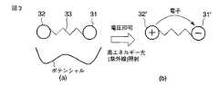
図3(a)および(b)に本発明の他の実施形態に係る量子ドット対を模式的に示す。図3(a)は電子受容性量子ドット31と電子供与性量子ドット32がアルキル鎖33によって連結されている量子ドット対を示す。電子受容性量子ドット31および電子供与性量子ドット32のポテンシャルは極小値をもち、両者の中間にはポテンシャルバリア(アルキル鎖33によるバリア層)が存在する。図3(b)に示すように、電圧を印加すると、電子がポテンシャルバリアを超えて電子供与性量子ドット32から電子受容性量子ドット31へ移動する。電子受容性量子ドット31はアニオン量子ドット31’となり、電子供与性量子ドット32はカチオン量子ドット32’となる。 3A and 3B schematically show a quantum dot pair according to another embodiment of the present invention. FIG. 3A shows a quantum dot pair in which an electron-accepting
例えばC60は中性状態もアニオン状態もカチオン状態も安定である。従って、C60の対をアルキル鎖で連結し、電圧を印加すると、一方がアニオン状態、他方がカチオン状態となって屈折率が変化する。この場合にも、正電荷と負電荷とが同時に生じ、全体では中性であるので、チャージアップすることはない。電圧を印加する場合、ポテンシャルバリアを超えやすくするため、紫外線などの高エネルギー光を照射すると、電子移動に要する電圧を低減できる。For example, C60 is stable in neutral, anionic and cationic states. Therefore, when a pair of C60 is connected by an alkyl chain and a voltage is applied, one becomes an anionic state and the other becomes a cationic state, and the refractive index changes. Also in this case, the positive charge and the negative charge are generated at the same time and are neutral as a whole, so that they are not charged up. When a voltage is applied, in order to easily exceed the potential barrier, irradiation with high energy light such as ultraviolet rays can reduce the voltage required for electron transfer.
図3の状態で、移動可能な電子がどちらかの量子ドットに存在する必要がある。このため、電子が双方の量子ドットに広がらないように、量子ドット間は上記のようにたとえばアルキル鎖で連結されていることが好ましい。ただし、量子ドット間の連結基は共役していなければよく、アルキル鎖に限定されない。 In the state of FIG. 3, movable electrons must be present in either quantum dot. For this reason, it is preferable that the quantum dots are connected by, for example, an alkyl chain as described above so that electrons do not spread to both quantum dots. However, the connecting group between the quantum dots is not limited and is not limited to the alkyl chain.
電子を発生する量子ドットとしてはホール輸送分子、ホール注入分子を使用できる。全体の屈折率変化はアニオン量子ドットの屈折率変化によってほぼ決定され、電子を注入した場合に屈折率変化が大きくなる。電子供与性量子ドットは中性状態とカチオン状態で屈折率が大きく変化することはなく、屈折率は大きくなる場合と小さくなる場合がある。屈折率変化への寄与という点ではアニオン量子ドットの影響が大きい。すなわち、アニオン量子ドットの特性がもっとも重要であり、アニオン量子ドットに応じて屈折率変化が大きくなったり小さくなったりする。単に分子内電荷移動が起これば屈折率変化が大きくなるというわけではない。 As a quantum dot that generates electrons, a hole transport molecule or a hole injection molecule can be used. The total refractive index change is almost determined by the refractive index change of the anion quantum dots, and the refractive index change becomes large when electrons are injected. The electron donating quantum dot does not change its refractive index greatly between the neutral state and the cationic state, and the refractive index may be increased or decreased. In terms of contribution to refractive index change, the influence of anion quantum dots is significant. That is, the characteristics of anion quantum dots are the most important, and the refractive index change increases or decreases depending on the anion quantum dots. If intramolecular charge transfer simply occurs, the change in refractive index does not increase.
本発明の実施形態において、量子ドット対を含む構造部へ電圧を印加する電圧印加部としては、たとえば構造部を挟む1対の電極や、近接場光学顕微鏡(Near-field Scanning Optical Microscope,NSOM)のプローブが挙げられる。 In the embodiment of the present invention, examples of the voltage application unit that applies a voltage to a structure including a quantum dot pair include a pair of electrodes sandwiching the structure, and a near-field scanning optical microscope (NSOM). These probes are mentioned.
電圧印加部が構造部を挟む1対の電極である場合、1対の電極のうち少なくとも一方は、構造部の一部に対応して設けられていてもよい。この場合、1対の電極のうち少なくとも一方を複数の部分に分割した形態とし、構造部の任意の一部を選択して電子移動させ、その部分の屈折率を選択的に変化させるようにしてもよい。 When the voltage application unit is a pair of electrodes sandwiching the structure unit, at least one of the pair of electrodes may be provided corresponding to a part of the structure unit. In this case, at least one of the pair of electrodes is divided into a plurality of parts, an arbitrary part of the structure part is selected and moved, and the refractive index of the part is selectively changed. Also good.
また、光で励起し、かつ電圧を印加した方がアニオン−カチオンの量子ドット対が発生する効率が高くなる。ただし、電圧印加のみまたは光励起のみでもアニオン−カチオンの量子ドット対を発生させることができる。 In addition, the efficiency of generating anion-cation quantum dot pairs increases when excited by light and applied with a voltage. However, anion-cation quantum dot pairs can be generated only by voltage application or photoexcitation.
電子印加部が構造部を挟む1対の電極である場合、光が電極間のみを伝播する場合には両方の電極が光不透過性であってもよい。また、電極を通して光を照射する場合も多いので、その場合は両方の電極が光透過性であるか、または一方の電極が光透過性で他方の電極が光不透過性である必要がある。 When the electron application part is a pair of electrodes sandwiching the structure part, when light propagates only between the electrodes, both electrodes may be light-impermeable. In many cases, light is irradiated through the electrodes. In this case, both electrodes must be light-transmitting, or one electrode must be light-transmitting and the other electrode light-impermeable.
本発明の実施形態において、電圧の印加によってアニオン状態の量子ドットとカチオン状態の量子ドットとの間で中間のバリア層を通過して電子が移動するメカニズムとしては、(1)バリアを超える電子移動、(2)トンネル効果、(3)ホッピング伝導が考えられる。例えば、(1)高電圧を加えた場合、電子はバリアを超えて移動しやすい。(2)バリア層(例えば、アルキル鎖)が十分薄い場合にはトンネリングが起こりやすい。(3)バリア層がアモルファスであるか不純物やイオンを含むものである場合には、局在する準位が形成され、ホッピングによって電子が移動する場合がある。 In the embodiment of the present invention, as a mechanism for moving electrons through an intermediate barrier layer between an anionic quantum dot and a cationic quantum dot by applying a voltage, (1) electron transfer exceeding the barrier (2) Tunnel effect and (3) Hopping conduction. For example, (1) When a high voltage is applied, electrons easily move across the barrier. (2) Tunneling tends to occur when the barrier layer (for example, alkyl chain) is sufficiently thin. (3) When the barrier layer is amorphous or contains impurities or ions, localized levels are formed, and electrons may move by hopping.
以下、(2)のトンネル効果についてより詳細に説明する。トンネル効果とは、量子力学的な系でポテンシャルV0の高さがあるバリアに、V0よりも小さいエネルギーEの電子が衝突した時にバリアを突き抜ける現象である。バリアの内側でも外側でも確率tがゼロでない場合に起こる。シュレディンガー方程式に従って計算すれば、バリアを通り抜ける透過率すなわちトンネル効果の確率tは下記の式で表わされる(「単一電子トンネリング概論」春山純志著、コロナ社、2002年初版参照)。
この式によると、バリアの厚みaが薄いほどトンネリングが起こり易いことがわかる。 According to this formula, it can be seen that tunneling is more likely to occur as the barrier thickness a decreases.
屈折率は基底準位(HOMO:Highest Occupied Molecular Orbital、SOMO:Single occupied molecular orbital)と励起準位(LUMO:Lowest Unoccupied Molecular Orbital)との間のエネルギーギャップの大きさに関係しており、これら2つの相対関係である。 The refractive index is related to the size of the energy gap between the ground level (HOMO: Highest Occupied Molecular Orbital, SOMO: Single occupied molecular orbital) and the excitation level (LUMO: Lowest Unoccupied Molecular Orbital). Is a relative relationship.
本発明の実施形態においては、アニオン−カチオン対が形成された後であれば電圧印加部がなくても構造部の屈折率変化の効果が維持されるので、電子注入後に電子注入部を取り外すことができる。 In the embodiment of the present invention, if the anion-cation pair is formed, the effect of changing the refractive index of the structure portion is maintained without the voltage application portion, so that the electron injection portion is removed after the electron injection. Can do.
本発明は屈折率変化の新しいメカニズムを提案するものであり、本発明の実施形態に係る屈折率変化素子ではこれまでの素子よりも大きな屈折率変化が得られる。 The present invention proposes a new mechanism for changing the refractive index, and the refractive index changing element according to the embodiment of the present invention can provide a larger refractive index change than the conventional elements.
本発明における屈折率変化のメカニズムは以下の通りである。量子ドットに電子を注入すると、屈折率の決定に大きく寄与する最外殻オービタル(すなわち最高被占分子軌道)の外側に、新たに最外殻オービタル(すなわちより高エネルギーの最高被占分子軌道)が形成され、このような量子ドットが固体マトリックスで囲まれていると大きな屈折率変化の効果を得ることができる。逆に、量子ドットから電子を排出すると、屈折率の決定に大きく寄与する最外殻オービタル(すなわち最高被占分子軌道)がなくなり、大きな屈折率変化の効果を得ることができる。 The mechanism of refractive index change in the present invention is as follows. When electrons are injected into a quantum dot, the outermost orbital (that is, the highest occupied molecular orbital) is newly added outside the outermost orbital (that is, the highest occupied molecular orbital) that greatly contributes to the determination of the refractive index. When such quantum dots are surrounded by a solid matrix, a large refractive index change effect can be obtained. Conversely, when electrons are ejected from the quantum dots, the outermost orbital (that is, the highest occupied molecular orbital) that greatly contributes to the determination of the refractive index disappears, and the effect of a large refractive index change can be obtained.
本発明の実施形態に係る屈折率変化素子の効果は、2次や3次の非線形光学効果によって構造部の屈折率変化を得る従来技術とは大きく異なる。両者の相違点について以下に説明する。 The effect of the refractive index changing element according to the embodiment of the present invention is significantly different from the conventional technique that obtains the refractive index change of the structure portion by the second-order or third-order nonlinear optical effect. Differences between the two will be described below.
(1)一般にフォトクロミズムなど吸収スペクトルを変化させる方法はいくつかある。また、クラマース=クロニッヒの関係が導くように、吸収端近傍における屈折率変化は比較的大きくできる。このため、吸収スペクトルまたは吸収係数を変化させて屈折率実部を変化させる方法はよく用いられている。しかし、透明領域においては大きく屈折率を変化させることは難しい。一方、本発明の実施形態においては、透明領域においても大きな屈折率変化をもたらすことができる。 (1) In general, there are several methods for changing the absorption spectrum such as photochromism. Further, as the Kramers-Kronig relationship leads, the refractive index change in the vicinity of the absorption edge can be made relatively large. For this reason, a method of changing the real part of the refractive index by changing the absorption spectrum or the absorption coefficient is often used. However, it is difficult to greatly change the refractive index in the transparent region. On the other hand, in the embodiment of the present invention, a large refractive index change can be brought about even in the transparent region.
(2)一般的な3次元のバルク半導体の場合、多数の電荷が同一励起バンド枝に存在するため、1個の電子を注入してもバンド(エネルギー準位)を占有する電子の分布の変化が非常に小さい。一方、本発明の実施形態では、量子ドットのエネルギー準位が離散化されているため、1個のエネルギー準位に存在できる電子の数は数えられる程度である。このため量子ドットに新たに1個の電子を注入した場合、電子はそれまで電子が存在していなかったエネルギー準位を占有する。また、量子ドットのエネルギー準位が離散化しているため、吸収スペクトルピークの幅が狭く透明領域が広い。 (2) In the case of a general three-dimensional bulk semiconductor, since a large number of charges exist in the same excitation band branch, the change in the distribution of electrons that occupy the band (energy level) even if one electron is injected. Is very small. On the other hand, in the embodiment of the present invention, since the energy levels of the quantum dots are discretized, the number of electrons that can exist in one energy level is only counted. For this reason, when one electron is newly injected into the quantum dot, the electron occupies an energy level that had not existed until then. In addition, since the energy level of the quantum dots is discretized, the width of the absorption spectrum peak is narrow and the transparent region is wide.
(3)本発明の実施形態に係る屈折率変化素子は、光を導波させることを目的とするものであり、この点で吸収や共鳴状態を伴うレーザーや増幅器とは異なる。従って、透明な波長領域が広ければ広いほど光デバイスとしての応用範囲は広くなる。さらに、本発明の実施形態は、吸収共鳴効果で3次非線形光学効果が増幅される量子ドット励起子効果とは原理も異なり、透明領域でも屈折率変化するという効果も異なる。 (3) The refractive index changing element according to the embodiment of the present invention is intended to guide light, and is different from a laser or an amplifier with an absorption or resonance state in this respect. Accordingly, the wider the transparent wavelength region, the wider the application range as an optical device. Furthermore, the embodiment of the present invention is different in principle from the quantum dot exciton effect in which the third-order nonlinear optical effect is amplified by the absorption resonance effect, and also has the effect that the refractive index changes even in the transparent region.
(4)本発明の実施形態では、量子ドット以外の固体マトリックスは屈折率変化しないため、量子ドットの密度が高いほど全体の平均屈折率変化が大きくなる。本発明の実施形態に係る屈折率変化素子を導波路として使用する場合、平均屈折率変化が少なくとも1.5%を超えるように量子ドットの密度を設定することが有効である。1.5%とは現在使用されている導波路の屈折率変化の一般的な値である。 (4) In the embodiment of the present invention, since the refractive index of the solid matrix other than the quantum dots does not change, the overall average refractive index change increases as the density of the quantum dots increases. When the refractive index changing element according to the embodiment of the present invention is used as a waveguide, it is effective to set the density of the quantum dots so that the average refractive index change exceeds at least 1.5%. 1.5% is a general value of the refractive index change of the currently used waveguide.
(5)従来技術では、電子は構造部に電場を加えるための電極にとどまっており、電子は量子ドットや分子内で分極するだけである。すなわち、従来技術ではバリア層は存在せず、当然、バリア層を超える電子移動もない。一方、本発明の実施形態では、量子ドット対の間のバリア層を超えて電子が移動する(なお、電子受容性の量子ドットと電子供与性の量子ドットが有機分子であってバリア層となるアルキル鎖などで連結されて1分子になっている場合、量子ドット対をなすその1分子中にバリア層が存在することになる)。 (5) In the prior art, electrons remain in the electrode for applying an electric field to the structure, and the electrons are only polarized in quantum dots or molecules. That is, in the prior art, there is no barrier layer and, of course, there is no electron transfer beyond the barrier layer. On the other hand, in the embodiment of the present invention, electrons move beyond the barrier layer between the quantum dot pairs (note that the electron-accepting quantum dots and the electron-donating quantum dots are organic molecules and become barrier layers. In the case where one molecule is connected by an alkyl chain or the like, a barrier layer is present in the molecule constituting the quantum dot pair).
(6)従来技術では、構造部に電圧を印加するのを停止したときに、非線形光学効果が失われ、屈折率変化効果も失われる。一方、本発明の実施形態に係るアニオン−カチオンの量子ドット対は、存続時間が有限であるものの一種の安定状態にあり、屈折率変化の効果が持続する。 (6) In the prior art, when the voltage application is stopped, the nonlinear optical effect is lost and the refractive index change effect is also lost. On the other hand, the anion-cation quantum dot pair according to the embodiment of the present invention is in a kind of stable state although its lifetime is finite, and the effect of refractive index change is sustained.
(7)従来技術のポッケルス効果では、屈折率変化の度合いはたかだか10-3程度である。一方、本発明の実施形態では、量子ドット対が高密度であれば屈折率変化の度合いは10-1またはそれ以上になる。逆に、従来と同程度の屈折率変化を起こすには、量子ドット対が低密度であってもよい。(7) In the Pockels effect of the prior art, the degree of refractive index change is at most about 10−3 . On the other hand, in the embodiment of the present invention, if the number of quantum dot pairs is high, the degree of refractive index change is 10−1 or more. Conversely, the quantum dot pair may have a low density in order to cause a refractive index change similar to the conventional one.
上記の相違点に関連してさらに原理的な説明を述べる。量子ドットへ入射した光はその電場によって、電子殻を揺らす(励起)。揺らされた電子殻は光を放出する。この時の放出過程はアインシュタインのB係数に関わるもので、非共鳴領域においても励起から放出までに時間を要する。励起と放出を繰り返すことによって、光は伝播していく。この励起・放出にかかる時間が光伝播の位相速度Vpを決定する。真空中の光速をCとするとVp/Cが、本発明において変化を起こそうとする屈折率実部である。既述したように屈折率はローレンツ−ローレンスの式を通して分子分極率と関係づけられる。 A more fundamental explanation will be given in relation to the above differences. The light incident on the quantum dot shakes the electron shell by its electric field (excitation). The shaken electron shell emits light. The emission process at this time relates to Einstein's B coefficient, and it takes time from excitation to emission even in a non-resonant region. Light is propagated by repeating excitation and emission. The time required for this excitation / emission determines the phase velocity Vp of light propagation. Assuming that the speed of light in vacuum is C, Vp / C is the real part of the refractive index that is going to change in the present invention. As described above, the refractive index is related to the molecular polarizability through the Lorentz-Lawrence equation.
従来は2次、3次の非線形光学効果を利用し、電場を印加することによって電子のオービタルを歪ませて分子分極率を変化させるという方法が一般的であった。しかし、この方法による分極率変化は小さい。一方、ナノスケールサイズの量子ドットに電子を注入した場合、新しくオービタルが形成され、かつクーロン反発がおこるため、HOMOやLUMOのケミカルポテンシャルやHOMO−LUMOギャップが大きく変動する。従ってこれらの効果により分極率が大きく変化する。なお、量子ドットから電子を排出した場合、新たなオービタルは形成されないため、電子を注入した場合に較べて屈折率の変化は小さい。それでも、従来技術である非線形光学効果による分極率変化に較べて大きな変化が期待できる。 Conventionally, a method of using a second-order or third-order nonlinear optical effect and distorting an orbital of electrons by applying an electric field to change the molecular polarizability is common. However, the change in polarizability by this method is small. On the other hand, when electrons are injected into nanoscale-sized quantum dots, new orbitals are formed and coulomb repulsion occurs, so that the chemical potential of HOMO and LUMO and the HOMO-LUMO gap vary greatly. Therefore, the polarizability changes greatly due to these effects. When electrons are ejected from the quantum dots, no new orbital is formed, so the change in the refractive index is smaller than when electrons are injected. Nevertheless, a large change can be expected compared to the change in polarizability due to the nonlinear optical effect that is the prior art.
(実施例1)
本実施例においては、真空マトリックス中に分散された各種中性量子ドットが電子1個を捕捉した際の電子分極率の変化率と、その際の屈折率の変化をシミュレーションした。平均分極率<P>はB3LYP/6-31+G*に基づいて計算した。得られた<P>の値からローレンツ−ローレンスの式によって屈折率を算出した。その際、各量子ドットの密度を15%または5%として計算した。電子捕捉前の分極率および屈折率を基準として、電子捕捉による分極率変化率および屈折率変化率(単位:倍)を計算した。表1にこれらの結果をまとめて示す。
In this example, the change rate of the electronic polarizability when various neutral quantum dots dispersed in the vacuum matrix captured one electron and the change of the refractive index at that time were simulated. The average polarizability <P> was calculated based on B3LYP / 6-31 + G* . The refractive index was calculated from the obtained <P> value by the Lorentz-Lawrence equation. At that time, the density of each quantum dot was calculated as 15% or 5%. Based on the polarizability and refractive index before electron capture, the polarizability change rate and refractive index change rate (unit: times) due to electron capture were calculated. Table 1 summarizes these results.
表1中、Ia族(Na,K)に属する金属塩からなる量子ドットでは、電子捕捉時のアニオンの平均分極率<P>が非常に大きいため、密度を15%とすると、ローレンツ−ローレンスの式による屈折率の算出ができなかった。これらの系では、密度を5%程度に下げても非常に大きな屈折率変化が起きることが示された。また、比較例のo−クロラニル(C6O2Cl4)では単一ドット(分子)の分極率変化率が11%程度であるために屈折率換算した場合にもわずかな変化率になっている。一方、本実施例中の他の量子ドットについてはいずれも、5%の密度でも1%以上の屈折率変化計算値が得られた。また、酢酸ナトリウム(CH3COOK)を比誘電率10.43の誘電体マトリックス中に分散させた場合の分極率変化を計算したところ、22.98倍という値が得られた。これは、表1に示した値に比べて僅かに小さくなっているが、この場合の電子捕捉による安定化エネルギー(酢酸ナトリウムの電子親和力)は、真空中の場合に比べて約1.5倍になった。従って、誘電体マトリックスを用いることで電荷捕捉した量子ドットがより安定化することが確認できた。In Table 1, since the average polarizability <P> of the anion at the time of electron capture is very large in a quantum dot made of a metal salt belonging to Group Ia (Na, K), when the density is 15%, Lorentz-Lawrence The refractive index could not be calculated by the formula. In these systems, it was shown that a very large refractive index change occurs even when the density is lowered to about 5%. Further, in the o-chloranil (C6 O2 Cl4 ) of the comparative example, the change rate of the polarizability of a single dot (molecule) is about 11%. Yes. On the other hand, for the other quantum dots in this example, a calculated value of refractive index change of 1% or more was obtained even at a density of 5%. Further, when the change in polarizability was calculated when sodium acetate (CH3 COOK) was dispersed in a dielectric matrix having a relative dielectric constant of 10.43, a value of 22.98 times was obtained. This is slightly smaller than the value shown in Table 1, but the stabilization energy (electron affinity of sodium acetate) by electron trapping in this case is about 1.5 times that in the vacuum. Became. Therefore, it was confirmed that the use of the dielectric matrix stabilizes the charge trapped quantum dots.
(実施例2)
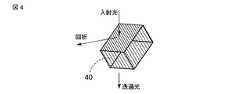
図4に示すように、量子ドット材料をポリマー中に均一に分散させて製膜した構造部40にレーザー光を照射して縞状に回折パターンを形成し、回折素子として用いられる屈折率変化素子を作製した。(Example 2)
As shown in FIG. 4, a refractive index changing element used as a diffraction element by forming a diffraction pattern in a stripe shape by irradiating a laser beam onto a
電荷発生機能とホール捕捉機能を有する量子ドットとして、下記化3に示すトリフェニルアミン誘導体を用いた。電子捕捉機能を有する量子ドットとして、表2に示すような化合物を用いた。それぞれの量子ドットを、密度が1.0mmol/cm3となるようにポリビニルアルコール中に均一に分散させ、1.0μmの膜厚に製膜した。これに波長350nmのレーザー光で回折縞を描いて回折素子を作製した。As a quantum dot having a charge generation function and a hole capturing function, a triphenylamine derivative represented by the following
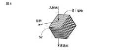
参照例として、図5に示すように、透明な多層の格子電極51の間に構造部52を挟んだ構造を有する屈折率変化素子を作製した。構造部52の材料として、下記化4に示す高分子液晶を1.0mmol/cm3の密度でポリスチレン中に均一に分散させたものを作製し、合計1.0μmの膜厚になるように積層した。各電極51に15Vの電圧を印加することにより、構造部52に電場を印加して回折素子を作製した。As a reference example, as shown in FIG. 5, a refractive index change element having a structure in which a
上記の回折素子に、波長900nmの光を照射し、回折光量を測定した。表2に、回折効率比を示す。表2に示されるように、本発明の材料系による量子ドットを用いると、参照例に比べて1桁以上大きな回折効率比が得られる。この結果から、本発明の屈折率変化素子では非常に大きい屈折率変化が得られることがわかった。
(実施例3)
電荷発生機能とホール捕捉機能を有する量子ドット(A)として、下記化5に示すトリフェニルアミン誘導体を用いた。電子捕捉機能を有する量子ドット(B)として、表3に示す6種類の分子を用いた。表3に、これらの分子の電子捕捉による分極率変化率(B3LYP/6-31+G*)を示す。マトリックス材としてはポリメチルメタクリレート(PMMA)を用いた。(Example 3)
As a quantum dot (A) having a charge generation function and a hole capturing function, a triphenylamine derivative represented by the following
蒸着温度は400℃、真空度は10-5Torrで真空蒸着を行い、ガラス基板上に、量子ドット(A)を含む層と、量子ドット(B)を含む層とを交互に各20層、合計40層積層して合計膜厚を1.0μmの構造部を形成した。Vacuum deposition is performed at a deposition temperature of 400 ° C. and a degree of vacuum of 10−5 Torr. On the glass substrate, 20 layers each including a quantum dot (A) layer and a quantum dot (B) layer are alternately arranged. A total of 40 layers were laminated to form a structure portion having a total film thickness of 1.0 μm.
図6に示すように、構造部60に対してフォトマスクを通して波長350nmで露光し、屈曲した導波路61のパターンを形成した。この導波路61にレーザー光(波長800nm)を入射した。導波路61の入口から見てレーザー光の光軸の延長線上に第1の光検出器62を設置し、導波路61の出口に第2の光検出器63を設置し、各光検出器での光量を測定した。 As shown in FIG. 6, the
表3に示すように、いずれの電子捕捉分子を用いた場合にも、第1の光検出器62では光は殆んど検出されず、第2の光検出器63では入射光の80〜90%の光量が検出された。このように、これらの屈折率変化素子は導波路として機能することが確認できた。
(実施例4)
実施例3で用いたのと同じ6種類の膜(構造部)を形成し、これらの膜をそれぞれITO電極で挟んだ素子を作製した。それぞれの素子の屈折率を、顕微エリプソメータを用いて測定した。次に、ITO電極から膜に20Vの電圧を1分間印加した後、再び屈折率を測定した。その結果、いずれの素子でも0.5%〜1%の屈折率増加が認められた。さらに、350nmの光を照射した後、再び屈折率を測定した。その結果、いずれの素子でも4.5%〜5.6%の屈折率の増加が認められた。(Example 4)
The same six types of films (structure parts) used in Example 3 were formed, and an element in which these films were sandwiched between ITO electrodes was produced. The refractive index of each element was measured using a microscopic ellipsometer. Next, after applying a voltage of 20 V from the ITO electrode to the film for 1 minute, the refractive index was measured again. As a result, an increase in refractive index of 0.5% to 1% was observed in any element. Furthermore, after irradiating 350 nm light, the refractive index was measured again. As a result, an increase in refractive index of 4.5% to 5.6% was observed in any element.
(実施例5)
量子ドット対として、下記化6に示すように、2つのC60をトリメチレン鎖(−C3H6−)で連結したものを用意した。この量子ドット対をポリスチレンに質量比50wt%で分散させた構造部を作製した。構造部の厚みは約100nm、300nm、1μmの3種類とした。図7に示すように、量子ドット対71を分散させた構造部70の両面を厚さ100nmのポリスチレン膜72で挟み、さらにこれらの積層体の両面を、ITO電極73を形成したガラス基板74で挟んで素子(実施例5)を作製した。構造部72の両面にポリスチレン膜73を設けたのは、ITO電極74から量子ドット対71へ電子が注入されないようにするためである。
As quantum dot pairs, as shown in the following Formula 6, the two C60 trimethylene chain - was prepared which was ligated (-C3 H6). A structure part in which this quantum dot pair was dispersed in polystyrene at a mass ratio of 50 wt% was produced. The thickness of the structure portion was set to three types of about 100 nm, 300 nm, and 1 μm. As shown in FIG. 7, both surfaces of the
比較のために、単独のC60量子ドットを実施例5と同じモル数となるようにポリスチレンに分散させた構造部を作製した。構造部の厚みは約100nm、300nm、1μmの3種類とした。図8に示すように、量子ドット81を分散させた構造部80の両面を、ITO電極73を形成したガラス基板74で挟んで素子(比較例5)を作製した。For comparison, a structure part in which a single C60 quantum dot was dispersed in polystyrene so as to have the same number of moles as in Example 5 was prepared. The thickness of the structure portion was set to three types of about 100 nm, 300 nm, and 1 μm. As shown in FIG. 8, an element (Comparative Example 5) was fabricated by sandwiching both surfaces of a
図7と図8との比較からわかるように、1対のITO電極73間の厚みは、実施例5の方が比較例5よりも200nm厚くなっている。 As can be seen from the comparison between FIG. 7 and FIG. 8, the thickness between the pair of
まず、350nmの光を照射しながら15Vの電圧印加を10秒間行い、実施例5では対をなす量子ドット間で電子を移動させ、比較例5では電極からC60量子ドットへ電子を注入した。その後、電圧印加を停止した。比較例5では、電圧印加により量子ドットへ注入された電子が、電圧印加を停止した後に抜ける現象(逆電流)が認められた。これは電子注入によりチャージアップのためであると考えられる。これに対して、実施例5では、電圧印加を停止した後にも逆電流は認められなかった。First, a voltage of 15 V was applied for 10 seconds while irradiating 350 nm light. In Example 5, electrons were moved between paired quantum dots, and in Comparative Example 5, electrons were injected from the electrodes intoC60 quantum dots. Thereafter, voltage application was stopped. In Comparative Example 5, a phenomenon (reverse current) in which electrons injected into the quantum dots by voltage application escape after the voltage application was stopped was observed. This is considered to be due to charge-up by electron injection. In contrast, in Example 5, no reverse current was observed even after the voltage application was stopped.
屈折率変化を顕微エリプソメータで測定した。屈折率変化は構造部の場所によって異なっていた。これは、構造部中に分散している量子ドットの分散質量比が場所によって異なるためである。ここでは、特定の構造部を有する素子で測定された最大の屈折率変化を採用している。電圧を切った後の屈折率変化率は、実施例5で6.5%、比較例5で5%であり、実施例5の方が比較例5より約30%高かった。 The refractive index change was measured with a micro ellipsometer. The refractive index change was different depending on the location of the structure. This is because the dispersion mass ratio of the quantum dots dispersed in the structure portion varies depending on the location. Here, the maximum refractive index change measured with an element having a specific structure is employed. The refractive index change rate after the voltage was turned off was 6.5% in Example 5 and 5% in Comparative Example 5, and Example 5 was about 30% higher than Comparative Example 5.
電圧印加時の屈折率変化速度を測定した。実施例5では、構造部の膜厚にかかわらず、屈折率変化速度は100nsec以下であった。比較例5では構造部の膜厚が100nmの場合でも屈折率変化速度は1μsec以上であり、構造部の膜厚が厚くなるに従って屈折率変化速度が遅くなった。 The refractive index change rate during voltage application was measured. In Example 5, the refractive index change rate was 100 nsec or less regardless of the film thickness of the structure portion. In Comparative Example 5, even when the thickness of the structure portion was 100 nm, the refractive index change rate was 1 μsec or more, and the refractive index change rate became slower as the thickness of the structure portion increased.
電圧を印加せずに、光照射のみを行い、屈折率変化を測定した。屈折率変化は、実施例5で2.0%、比較例5で1.4%であった。光照射なしで電圧印加を1分間行い、屈折率変化を測定した。屈折率変化は、実施例5で6.5%、比較例5で5%であった。光照射があった場合とほぼ同様な結果を得た。どちらの条件でも、屈折率変化率は実施例5の方が比較例5より高いという同様な傾向が認められた。 Only a light irradiation was performed without applying a voltage, and a change in refractive index was measured. The refractive index change was 2.0% in Example 5 and 1.4% in Comparative Example 5. Voltage application was performed for 1 minute without light irradiation, and the refractive index change was measured. The refractive index change was 6.5% in Example 5 and 5% in Comparative Example 5. The result was almost the same as when light was irradiated. Under either condition, the same tendency was observed that the refractive index change rate was higher in Example 5 than in Comparative Example 5.
(実施例6)
表4に示す量子ドット対をPMMA中に質量比50wt%の比率で分散して厚さ1μmの構造部を作製し、ITO電極で挟んだ。まず、顕微エリプソメータを用いて屈折率測定を行った。その後、350nmの光を照射しながら15Vの電圧印加を10秒間行った後、再び屈折率測定を行った。表4に屈折率変化を併記する。
A quantum dot pair shown in Table 4 was dispersed in PMMA at a mass ratio of 50 wt% to produce a structure portion having a thickness of 1 μm and sandwiched between ITO electrodes. First, the refractive index was measured using a microscopic ellipsometer. Thereafter, a voltage of 15 V was applied for 10 seconds while irradiating 350 nm light, and then the refractive index was measured again. Table 4 shows changes in refractive index.
(実施例7)
前記化3に示すトリフェニルアミン誘導体のメチル基とCH3COONaのメチル基をトリメチレン鎖で連結した量子ドット対を、ポリビニルアルコール(PVA)に10wt%の割合で分散させて構造部を作製した。構造部の両面を厚さ100nmのPVA膜で挟み、さらにこれらの積層体の両面を、ITO電極を形成したガラス基板で挟んで素子を作製した。(Example 7)
A quantum dot pair obtained by connecting the methyl group of the triphenylamine derivative shown in Chemical Formula3 and the methyl group of CH3 COONa with a trimethylene chain was dispersed in polyvinyl alcohol (PVA) at a rate of 10 wt% to prepare a structure part. A device was fabricated by sandwiching both surfaces of the structure portion with a PVA film having a thickness of 100 nm, and sandwiching both surfaces of the laminate with a glass substrate on which an ITO electrode was formed.
320nmの光を照射しながら20Vの電圧を1分間印加し、顕微エリプソメータで屈折率変化を測定した。その結果、最高で1.2%の屈折率変化が観測された。光照射のみ1分間行った場合には、0.6%の屈折率変化が観測された。20Vの電圧印加を1分間行った場合には、1.0%の屈折率変化が観測された。 A voltage of 20 V was applied for 1 minute while irradiating light of 320 nm, and the refractive index change was measured with a microscopic ellipsometer. As a result, a maximum refractive index change of 1.2% was observed. When only light irradiation was performed for 1 minute, a refractive index change of 0.6% was observed. When a voltage of 20 V was applied for 1 minute, a refractive index change of 1.0% was observed.
トリフェニルアミンの代わりに、テトラフェニルシクロペンタジエン、ヘキサフェニルベンゼン、ジフェニルアントラセン、またはルブレンを、CH3COONaに連結させた以外は上記と同様にして、素子を作製した。300nmの光を照射しながら20Vの電圧を印加して屈折率変化率を測定した結果、それぞれ1.1%、1.0%、1.5%、1.2%であった。A device was fabricated in the same manner as described above except that tetraphenylcyclopentadiene, hexaphenylbenzene, diphenylanthracene, or rubrene was linked to CH3 COONa instead of triphenylamine. As a result of measuring the refractive index change rate by applying a voltage of 20 V while irradiating 300 nm light, they were 1.1%, 1.0%, 1.5% and 1.2%, respectively.
CH3COONaの代わりにCH3COOKを用い、電子発生部位にトリフェニルアミン誘導体、テトラフェニルシクロペンタジエン、ヘキサフェニルベンゼン、ジフェニルアントラセン、またはルブレンを用いた以外は上記と同様にして、素子を作製した。300nmの光を照射しながら20Vの電圧を印加して屈折率変化率を測定した結果、それぞれ1.8%、1.6%、1.5%、2.2%、1.8%であった。A device was fabricated in the same manner as above except that CH3 COOK was used instead of CH3 COONa, and a triphenylamine derivative, tetraphenylcyclopentadiene, hexaphenylbenzene, diphenylanthracene, or rubrene was used as the electron generation site. . As a result of measuring the refractive index change rate by applying a voltage of 20 V while irradiating 300 nm light, it was 1.8%, 1.6%, 1.5%, 2.2%, and 1.8%, respectively. It was.
10…構造部、11…電荷発生機能を有する量子ドット、12…電子捕捉機能を有する量子ドット、13…ホール捕捉機能を有する量子ドット、20…構造部、21…光照射部、25…フォトマスク、31…電子受容性量子ドット、31’…アニオン量子ドット、32…電子供与性量子ドット、32’…カチオン量子ドット、33…アルキル鎖、40…構造部、51…電極、52…構造部、60…構造部、61…導波路、62…第1の光検出器、63…第2の光検出器、70…構造部、71…量子ドット対、72…ポリスチレン膜、73…ITO電極、74…ガラス基板、80…構造部、81…量子ドット。 DESCRIPTION OF
Claims (7)
Translated fromJapanese前記量子ドットは光照射によって正負一対の電荷を発生する機能と正電荷を捕捉する機能と負電荷を捕捉する機能を有し、
前記負電荷を捕捉する機能を有する量子ドットは、電子注入により占有軌道の電子殻の変化をともなう元素のカチオンとアクセプターの組み合わせ、金属キレート錯体、ならびにメタロセンおよびその誘導体からなる群より選択されることを特徴とする屈折率変化素子。Having a structure in which one or more types of quantum dots having discrete occupied and unoccupied electron energy levels are dispersed in a solid matrix;
The quantum dot has a function of generating a pair of positive and negative charges by light irradiation, a function of capturing a positive charge, and a function of capturing a negative charge,
The quantum dot having a function of capturing a negative charge is selected from the group consisting of a combination of an element cation and an acceptor, a metal chelate complex, and a metallocene and a derivative thereof accompanied by a change in an electron shell of an occupied orbit by electron injection. Refractive index change element characterized by the above.
前記量子ドットは光照射によって正負一対の電荷を発生する機能と正電荷を捕捉する機能と負電荷を捕捉する機能を有し、
前記負電荷を捕捉する機能を有する量子ドットは負電荷を捕捉した際の電子分極率の変化を分子軌道法のB3LYP/6-31+G*で計算した計算値が20%以上であることを特徴とする屈折率変化素子。Having a structure in which one or more types of quantum dots having discrete occupied and unoccupied electron energy levels are dispersed in a solid matrix;
The quantum dot has a function of generating a pair of positive and negative charges by light irradiation, a function of capturing a positive charge, and a function of capturing a negative charge,
The quantum dot having the function of trapping the negative charge has a calculated value calculated by B3LYP / 6-31 + G* of the molecular orbital method of the change of the electronic polarizability when the negative charge is trapped is 20% or more. Refractive index change element characterized.
前記構造部へ電圧を印加する電圧印加部と
を有することを特徴とする屈折率変化素子。In a solid matrix, a structure in which an electron-accepting quantum dot that becomes an anion and an electron-donating quantum dot that becomes a cation are paired and a quantum dot pair in which electrons can move between both quantum dots is dispersed When,
A refractive index changing element, comprising: a voltage application unit that applies a voltage to the structure unit.
Priority Applications (2)
| Application Number | Priority Date | Filing Date | Title |
|---|---|---|---|
| JP2005157529AJP4372048B2 (en) | 2005-05-30 | 2005-05-30 | Refractive index change element |
| US11/441,092US7732806B2 (en) | 2005-05-30 | 2006-05-26 | Refractive index variable element |
Applications Claiming Priority (1)
| Application Number | Priority Date | Filing Date | Title |
|---|---|---|---|
| JP2005157529AJP4372048B2 (en) | 2005-05-30 | 2005-05-30 | Refractive index change element |
Publications (2)
| Publication Number | Publication Date |
|---|---|
| JP2006330596A JP2006330596A (en) | 2006-12-07 |
| JP4372048B2true JP4372048B2 (en) | 2009-11-25 |
Family
ID=37523869
Family Applications (1)
| Application Number | Title | Priority Date | Filing Date |
|---|---|---|---|
| JP2005157529AExpired - Fee RelatedJP4372048B2 (en) | 2005-05-30 | 2005-05-30 | Refractive index change element |
Country Status (2)
| Country | Link |
|---|---|
| US (1) | US7732806B2 (en) |
| JP (1) | JP4372048B2 (en) |
Families Citing this family (17)
| Publication number | Priority date | Publication date | Assignee | Title |
|---|---|---|---|---|
| JP2007328188A (en)* | 2006-06-08 | 2007-12-20 | Toshiba Corp | Near-field interaction control element |
| JP4469871B2 (en)* | 2007-03-28 | 2010-06-02 | 株式会社東芝 | Optical waveguide |
| JP4477052B2 (en) | 2007-10-03 | 2010-06-09 | 株式会社東芝 | Method for producing metal nanoparticle inorganic composite and metal nanoparticle inorganic composite |
| ATE530342T1 (en)* | 2008-01-28 | 2011-11-15 | Hitachi Ind Equipment Sys | INKJET RECORDING APPARATUS |
| WO2009145813A1 (en) | 2008-03-04 | 2009-12-03 | Qd Vision, Inc. | Particles including nanoparticles, uses thereof, and methods |
| JP4595007B2 (en)* | 2008-07-23 | 2010-12-08 | 株式会社東芝 | Optical waveguide system |
| JP4477083B2 (en)* | 2008-09-24 | 2010-06-09 | 株式会社東芝 | Method for producing metal nanoparticle inorganic composite, metal nanoparticle inorganic composite, and plasmon waveguide |
| US20100264371A1 (en)* | 2009-03-19 | 2010-10-21 | Nick Robert J | Composition including quantum dots, uses of the foregoing, and methods |
| WO2011031876A1 (en) | 2009-09-09 | 2011-03-17 | Qd Vision, Inc. | Formulations including nanoparticles |
| CN102482457B (en) | 2009-09-09 | 2015-04-15 | Qd视光有限公司 | Particles including nanoparticles, uses thereof, and methods |
| JP6244092B2 (en)* | 2013-02-27 | 2017-12-06 | 三井化学株式会社 | Optical materials and applications |
| CN106356463B (en)* | 2016-10-11 | 2017-12-29 | 深圳市华星光电技术有限公司 | The preparation method of QLED display devices |
| WO2018221978A1 (en)* | 2017-05-31 | 2018-12-06 | Rohm And Haas Electronic Materials Korea Ltd. | Organic electroluminescent device |
| KR102641027B1 (en) | 2017-05-31 | 2024-02-28 | 롬엔드하스전자재료코리아유한회사 | Organic Electroluminescent Device |
| CN108983446B (en)* | 2017-06-01 | 2021-04-06 | Tcl科技集团股份有限公司 | Light intensity modulator |
| CN107817637B (en)* | 2017-12-15 | 2020-09-22 | 合肥京东方光电科技有限公司 | Anti-blue light structure, display device and anti-blue light adjustment method |
| NL2024294B1 (en)* | 2019-11-22 | 2021-08-26 | Lusoco B V | Luminescent optical device and luminescent ink composition |
Family Cites Families (9)
| Publication number | Priority date | Publication date | Assignee | Title |
|---|---|---|---|---|
| JPH05289123A (en) | 1992-04-14 | 1993-11-05 | Ricoh Co Ltd | Surface optical modulator |
| US5936258A (en)* | 1995-04-28 | 1999-08-10 | Fujitsu Limited | Optical semiconductor memory device and read/write method therefor |
| US6005707A (en) | 1997-11-21 | 1999-12-21 | Lucent Technologies Inc. | Optical devices comprising polymer-dispersed crystalline materials |
| JP2002217488A (en) | 2001-01-19 | 2002-08-02 | Ricoh Co Ltd | Surface emitting laser element, surface emitting laser system, wavelength adjusting method, surface emitting laser array, optical interconnection system, and local area network system |
| JP3720277B2 (en) | 2001-05-02 | 2005-11-24 | 独立行政法人科学技術振興機構 | Polymer photoresponsive material and photoresponsive device using photoinduced electron transfer reaction |
| US20030066998A1 (en)* | 2001-08-02 | 2003-04-10 | Lee Howard Wing Hoon | Quantum dots of Group IV semiconductor materials |
| JP2005228899A (en)* | 2004-02-13 | 2005-08-25 | Kyoto Univ | Semiconductor quantum dot and fine wiring forming method, semiconductor device using the same, and manufacturing method thereof |
| JP4383996B2 (en) | 2004-09-29 | 2009-12-16 | 株式会社東芝 | Refractive index changing device and refractive index changing method |
| JP3987519B2 (en) | 2004-09-30 | 2007-10-10 | 株式会社東芝 | Refractive index changing device and refractive index changing method |
- 2005
- 2005-05-30JPJP2005157529Apatent/JP4372048B2/ennot_activeExpired - Fee Related
- 2006
- 2006-05-26USUS11/441,092patent/US7732806B2/ennot_activeExpired - Fee Related
Also Published As
| Publication number | Publication date |
|---|---|
| US20060279833A1 (en) | 2006-12-14 |
| US7732806B2 (en) | 2010-06-08 |
| JP2006330596A (en) | 2006-12-07 |
Similar Documents
| Publication | Publication Date | Title |
|---|---|---|
| JP4372048B2 (en) | Refractive index change element | |
| Gu et al. | Nanomaterials for optical data storage | |
| JP3431386B2 (en) | Recording element and drift mobility modulation element | |
| Lynn et al. | Photorefractive polymers for holography | |
| Moerner et al. | Polymeric photorefractive materials | |
| JP4383996B2 (en) | Refractive index changing device and refractive index changing method | |
| Achimova | Direct surface relief formation in nanomultilayers based on chalcogenide glasses: A review | |
| Nandakumar et al. | Quantum size effects on the third order optical nonlinearity of CdS quantum dots in Nafion | |
| JP4018417B2 (en) | Optical recording medium and optical recording apparatus | |
| Merkel et al. | Understanding the formation of surface relief gratings in azopolymers: A combined molecular dynamics and experimental study | |
| Shelkovnikov et al. | Nanometer films of polymethine dyes in optical memory and nonlinear optics | |
| US20030123117A1 (en) | Method for optical date recording | |
| JP3532743B2 (en) | Optical recording method | |
| JP3842570B2 (en) | Optical recording medium and optical recording apparatus | |
| JP3472063B2 (en) | Optical recording medium | |
| Hamodi et al. | Spatial self-phase modulation in plasmon excited Graphene/WS2 heterostructure | |
| Peyghambarian et al. | Photorefractive, Electro-Optical and Nonlinear Optical Properties of Conjugated Polymers | |
| JP3472186B2 (en) | Optical recording medium and optical recording device | |
| Lynn | Geometry and fluence effects on photorefractive polymer devices for holography | |
| Van Stryland et al. | Engineered Multifunctional Nanophotonic Materials for Ultrafast Optical Switching | |
| Shcherbin et al. | Resonant enhancement of photorefraction in CdTe via excitation of appropriate space-charge waves | |
| Kamanina et al. | Spectral and nonlinear optical properties of fullerene-doped pi-conjugated organic systems | |
| Li | Nanoparticle-based multi-dimensional optical data storage | |
| Shen | Near-field study of nonlinear optical interactions and its applications | |
| Martin et al. | Design guidelines for molecules with large hyperpolarizabili-ties for third-order nonlinear optics |
Legal Events
| Date | Code | Title | Description |
|---|---|---|---|
| A621 | Written request for application examination | Free format text:JAPANESE INTERMEDIATE CODE: A621 Effective date:20061024 | |
| A977 | Report on retrieval | Free format text:JAPANESE INTERMEDIATE CODE: A971007 Effective date:20090223 | |
| TRDD | Decision of grant or rejection written | ||
| A01 | Written decision to grant a patent or to grant a registration (utility model) | Free format text:JAPANESE INTERMEDIATE CODE: A01 Effective date:20090804 | |
| A01 | Written decision to grant a patent or to grant a registration (utility model) | Free format text:JAPANESE INTERMEDIATE CODE: A01 | |
| A61 | First payment of annual fees (during grant procedure) | Free format text:JAPANESE INTERMEDIATE CODE: A61 Effective date:20090901 | |
| FPAY | Renewal fee payment (event date is renewal date of database) | Free format text:PAYMENT UNTIL: 20120911 Year of fee payment:3 | |
| FPAY | Renewal fee payment (event date is renewal date of database) | Free format text:PAYMENT UNTIL: 20120911 Year of fee payment:3 | |
| FPAY | Renewal fee payment (event date is renewal date of database) | Free format text:PAYMENT UNTIL: 20120911 Year of fee payment:3 | |
| FPAY | Renewal fee payment (event date is renewal date of database) | Free format text:PAYMENT UNTIL: 20130911 Year of fee payment:4 | |
| LAPS | Cancellation because of no payment of annual fees |