JP4371739B2 - Electronic device having serial ATA interface and power saving method of serial ATA bus - Google Patents
Electronic device having serial ATA interface and power saving method of serial ATA busDownload PDFInfo
- Publication number
- JP4371739B2 JP4371739B2JP2003310361AJP2003310361AJP4371739B2JP 4371739 B2JP4371739 B2JP 4371739B2JP 2003310361 AJP2003310361 AJP 2003310361AJP 2003310361 AJP2003310361 AJP 2003310361AJP 4371739 B2JP4371739 B2JP 4371739B2
- Authority
- JP
- Japan
- Prior art keywords
- mode
- command
- serial ata
- power save
- host
- Prior art date
- Legal status (The legal status is an assumption and is not a legal conclusion. Google has not performed a legal analysis and makes no representation as to the accuracy of the status listed.)
- Expired - Lifetime
Links
Images


Classifications
- G—PHYSICS
- G06—COMPUTING OR CALCULATING; COUNTING
- G06F—ELECTRIC DIGITAL DATA PROCESSING
- G06F1/00—Details not covered by groups G06F3/00 - G06F13/00 and G06F21/00
- G06F1/26—Power supply means, e.g. regulation thereof
- G06F1/32—Means for saving power
- G06F1/3203—Power management, i.e. event-based initiation of a power-saving mode
- G06F1/3206—Monitoring of events, devices or parameters that trigger a change in power modality
- G06F1/3228—Monitoring task completion, e.g. by use of idle timers, stop commands or wait commands
- G—PHYSICS
- G06—COMPUTING OR CALCULATING; COUNTING
- G06F—ELECTRIC DIGITAL DATA PROCESSING
- G06F1/00—Details not covered by groups G06F3/00 - G06F13/00 and G06F21/00
- G06F1/26—Power supply means, e.g. regulation thereof
- G06F1/32—Means for saving power
- G06F1/3203—Power management, i.e. event-based initiation of a power-saving mode
- G06F1/3234—Power saving characterised by the action undertaken
- G06F1/325—Power saving in peripheral device
- G06F1/3268—Power saving in hard disk drive
- G—PHYSICS
- G06—COMPUTING OR CALCULATING; COUNTING
- G06F—ELECTRIC DIGITAL DATA PROCESSING
- G06F3/00—Input arrangements for transferring data to be processed into a form capable of being handled by the computer; Output arrangements for transferring data from processing unit to output unit, e.g. interface arrangements
- G06F3/06—Digital input from, or digital output to, record carriers, e.g. RAID, emulated record carriers or networked record carriers
- G06F3/0601—Interfaces specially adapted for storage systems
- G06F3/0668—Interfaces specially adapted for storage systems adopting a particular infrastructure
- G06F3/0671—In-line storage system
- G06F3/0673—Single storage device
- Y—GENERAL TAGGING OF NEW TECHNOLOGICAL DEVELOPMENTS; GENERAL TAGGING OF CROSS-SECTIONAL TECHNOLOGIES SPANNING OVER SEVERAL SECTIONS OF THE IPC; TECHNICAL SUBJECTS COVERED BY FORMER USPC CROSS-REFERENCE ART COLLECTIONS [XRACs] AND DIGESTS
- Y02—TECHNOLOGIES OR APPLICATIONS FOR MITIGATION OR ADAPTATION AGAINST CLIMATE CHANGE
- Y02D—CLIMATE CHANGE MITIGATION TECHNOLOGIES IN INFORMATION AND COMMUNICATION TECHNOLOGIES [ICT], I.E. INFORMATION AND COMMUNICATION TECHNOLOGIES AIMING AT THE REDUCTION OF THEIR OWN ENERGY USE
- Y02D10/00—Energy efficient computing, e.g. low power processors, power management or thermal management
- Y—GENERAL TAGGING OF NEW TECHNOLOGICAL DEVELOPMENTS; GENERAL TAGGING OF CROSS-SECTIONAL TECHNOLOGIES SPANNING OVER SEVERAL SECTIONS OF THE IPC; TECHNICAL SUBJECTS COVERED BY FORMER USPC CROSS-REFERENCE ART COLLECTIONS [XRACs] AND DIGESTS
- Y02—TECHNOLOGIES OR APPLICATIONS FOR MITIGATION OR ADAPTATION AGAINST CLIMATE CHANGE
- Y02D—CLIMATE CHANGE MITIGATION TECHNOLOGIES IN INFORMATION AND COMMUNICATION TECHNOLOGIES [ICT], I.E. INFORMATION AND COMMUNICATION TECHNOLOGIES AIMING AT THE REDUCTION OF THEIR OWN ENERGY USE
- Y02D30/00—Reducing energy consumption in communication networks
- Y02D30/50—Reducing energy consumption in communication networks in wire-line communication networks, e.g. low power modes or reduced link rate
Landscapes
- Engineering & Computer Science (AREA)
- Theoretical Computer Science (AREA)
- Physics & Mathematics (AREA)
- General Engineering & Computer Science (AREA)
- General Physics & Mathematics (AREA)
- Power Sources (AREA)
- Signal Processing For Digital Recording And Reproducing (AREA)
Description
Translated fromJapanese本発明は、シリアルATA(AT Attachment)インタフェースを持つ電子機器に係り、特にシリアルATAインタフェースの規格に準拠したシリアルATAバスのパワーセーブに好適な、ディスクドライブに代表される電子機器及びシリアルATAバスのパワーセーブ方法に関する。 The present invention relates to an electronic device having a serial ATA (AT Attachment) interface, and particularly suitable for power saving of a serial ATA bus compliant with the serial ATA interface standard, and an electronic device represented by a disk drive and a serial ATA bus. It relates to the power saving method.
現在、ディスクドライブの新インタフェースであるシリアルATAインタフェースの規格が策定中である。シリアルATAインタフェースは、従来のATAインタフェース(つまりパラレルATAインタフェース)と同様に、磁気ディスクドライブに代表される周辺機器とホストシステム(ホスト)との間のインタフェースとして用いられる。 Currently, a standard for the serial ATA interface, which is a new interface for disk drives, is being formulated. The serial ATA interface is used as an interface between a peripheral device represented by a magnetic disk drive and a host system (host) in the same manner as a conventional ATA interface (that is, a parallel ATA interface).
シリアルATAインタフェースを持つ周辺機器、例えば磁気ディスクドライブ(以下、HDDと称する)は、ホストとシリアルATAバスにより接続される。このようなHDDでは、従来のATAインタフェースとの互換性を確保するために、従来のATAインタフェースをシリアルATAインタフェースに、そしてシリアルATAインタフェースを従来のATAインタフェースに、それぞれ変換する必要がある。このようなインタフェース変換は、例えばシリアルATAブリッジと呼ばれるLSI(ブリッジLSI)で行われる。 A peripheral device having a serial ATA interface, for example, a magnetic disk drive (hereinafter referred to as HDD) is connected to the host via a serial ATA bus. In such an HDD, it is necessary to convert the conventional ATA interface into a serial ATA interface and the serial ATA interface into a conventional ATA interface in order to ensure compatibility with the conventional ATA interface. Such interface conversion is performed by, for example, an LSI (bridge LSI) called a serial ATA bridge.
シリアルATA規格では、機能別に3つの層、つまりPHY(Physcal Layer)層(物理層)、LINK層(リンク層)及びトランスポート(Transport)層が定義されている。PHY層は高速の信号送受信を実行する機能を持つ部分であり、受信内容を解釈してLINK層に伝達し、またLINK層からの要求に応じて信号の出力を実施する。LINK層はTransport層(トランスポート層)からの要求内容に応じてPHY層に信号出力の要求を出し、またPHY層からの受信入力をTransport層へ伝達する。Transport層は従来のATA規格における動作への変換を行う。このTransport層の役割は、従来のATA接続の場合と比較すると、ブリッジLSIが磁気ディスクドライブに用いられたとき、ホスト側のATA信号出力を行う部分に相当する。このブリッジLSIとHDD内のディスクコントローラ(HDC)との間は、従来のATAインタフェース規格に準拠したATAバス(またはそれに準じたバス)で接続される。このためブリッジLSIとHDD内のHDCとの間の接続部分は、従来のATAインタフェース規格と同等の、またはそれに準じた動作となる。このように、シリアルATAインタフェースにおいては、論理的コマンド等のプロトコルについては従来のATA規格との互換性を有する一方、従来パラレルで接続されていた部分がシリアル信号に変換されるる。 In the serial ATA standard, three layers, that is, a PHY (Physical Layer) layer (physical layer), a LINK layer (link layer), and a transport layer are defined for each function. The PHY layer is a part having a function of executing high-speed signal transmission / reception, interprets the received content and transmits it to the LINK layer, and outputs a signal in response to a request from the LINK layer. The LINK layer issues a signal output request to the PHY layer according to the request content from the transport layer (transport layer), and transmits the reception input from the PHY layer to the transport layer. The Transport layer performs conversion to the operation in the conventional ATA standard. The role of the transport layer corresponds to a portion that outputs the ATA signal on the host side when the bridge LSI is used in the magnetic disk drive, as compared with the case of the conventional ATA connection. The bridge LSI and the disk controller (HDC) in the HDD are connected by an ATA bus (or a bus conforming thereto) conforming to the conventional ATA interface standard. Therefore, the connection portion between the bridge LSI and the HDC in the HDD operates equivalent to or equivalent to the conventional ATA interface standard. As described above, in the serial ATA interface, a protocol such as a logical command is compatible with the conventional ATA standard, while a portion connected in parallel in the past is converted into a serial signal.
シリアルATAインタフェースでは、従来のATAインタフェース(つまりパラレルATAインタフェース)の規格に準拠したパワーセーブの状態(モード)の他に、周辺機器とホストとを接続するシリアルATAバス自体を対象としてパワーセーブする状態が定義されている。このシリアルATAバス自体のパワーをセーブするという概念は従来のATA規格では存在しない。 In the serial ATA interface, in addition to the power saving state (mode) based on the standard of the conventional ATA interface (that is, the parallel ATA interface), the power saving is performed for the serial ATA bus itself that connects the peripheral device and the host. Is defined. The concept of saving the power of the serial ATA bus itself does not exist in the conventional ATA standard.
シリアルATAインタフェースの規格では、シリアルATAインタフェースの電力管理モードとして、“PHY READY(IDLE)”,“PARTIAL(パーシャル)”及び“SLUMBER(スランバ)”の3種類が定義されている。“PHY READY”モードとは、PHY層の動作を実現する回路(PHY回路)と主PLL(Phase-Locked Loop)回路とが動作し、ホスト側及び周辺機器側の各々のインタフェース状態が同期している状態をいう。“PARTIAL”及び“SLUMBER”モードとは、PHY回路は動作しているが、インタフェース信号は中立になっている状態をいう。 In the serial ATA interface standard, three types of power management modes of the serial ATA interface are defined: “PHY READY (IDLE)”, “PARTIAL (partial)”, and “SLUMBER (slumber)”. In “PHY READY” mode, the circuit that realizes the operation of the PHY layer (PHY circuit) and the main PLL (Phase-Locked Loop) circuit operate, and the interface states of the host side and the peripheral device side are synchronized. The state that is. “PARTIAL” and “SLUMBER” modes are states in which the PHY circuit is operating but the interface signal is neutral.
“PARTIAL”及び“SLUMBER”モードの定義上の違いは、それらのモードから“PHY READY(IDLE)”モードへの復帰時間にある。即ち、“PARTIAL”モードでは、当該モードからの復帰時間は10μsを超えてはならないと定義されている。これに対し、“SLUMBER”モードでは、当該モードからの復帰時間は10msを超えてはならないと定義されている。“PARTIAL”または“SLUMBER”モードで、機器内のどの部分の省電力機能を動作させるか(つまり、どの回路の電源を遮断するか)は、復帰時間、インタフェースの電源状態を遵守している限り製造者側で任意に規定できる。 The difference in definition between the “PARIAL” and “SLUMBER” modes is the return time from these modes to the “PHY READY (IDLE)” mode. That is, in the “PARIAL” mode, it is defined that the return time from the mode should not exceed 10 μs. On the other hand, in the “SLUMBER” mode, it is defined that the return time from the mode should not exceed 10 ms. In which part of the device the power saving function is to be operated in the “PARIAL” or “SLUMBER” mode (that is, which circuit power is cut off) as long as the recovery time and the power status of the interface are observed. It can be arbitrarily defined by the manufacturer.
従来のATAインタフェース規格に準拠したパワーセーブ(つまりATAパワーセーブ)の状態への遷移は、基本的には、ホスト側の主導により実現される。このATAパワーセーブの状態として、“IDLE(アイドル)”,“STANDBY(スタンバイ)”及び“SLEEP(スリープ)”等が定義されている。これに対し、シリアルATAインタフェース規格に準拠したシリアルATAバス自体のパワーセーブ(つまりシリアルATAパワーセーブ)の状態(“PARTIAL”または“SLUMBER”)への遷移は、ホスト側または周辺機器側のどちらの主導によって実現されても構わない。しかし、シリアルATAパワーセーブの状態を制御する技術(特にATAパワーセーブの状態にシリアルATAパワーセーブの状態を連携させる技術)に関しては、シリアルATAインタフェースの規格が策定中であることから、従来は何も知られておらず、文献も存在しない。 The transition to the power save (that is, ATA power save) state based on the conventional ATA interface standard is basically realized by the host side. As the ATA power save state, “IDLE (idle)”, “STANDBY (standby)”, “SLEEP (sleep)”, and the like are defined. On the other hand, the transition to the power saving state of the serial ATA bus itself (ie, serial ATA power saving) (“PARIAL” or “SLUMBER”) conforming to the serial ATA interface standard can be made on either the host side or the peripheral device side. It may be realized by initiative. However, regarding the technology for controlling the status of the serial ATA power save (particularly the technology for linking the status of the serial ATA power save to the status of the ATA power save), the standard of the serial ATA interface is being formulated. Is not known and there is no literature.
上記したように、HDDのインタフェースにシリアルATAインタフェースを適用して当該HDDをシリアルATAバスによりホストと接続する場合、HDDには、従来のATAインタフェースをシリアルATAインタフェースに変換するシリアルATAインタフェース制御回路回路(シリアルATAブリッジ)を設ける必要がある。このようなHDDでは、シリアルATAインタフェース制御回路とHDDのディスクコントローラ(HDC)との接続部分の動作は、従来のATAインタフェース規格と同等、またはそれに準じた動作となる。このため、ディスクコントローラからは、シリアルATAブリッジが、命令を発行するホストであるかのように認識される。よって、HDDにおけるシリアルATAブリッジ周辺を除く部分の動作は従来のHDDと変わらない。このシリアルATAインタフェースを適用するHDDでは、シリアルATAインタフェース制御回路とディスクコントローラ(HDC)とを接続する従来のATAバスは、当該HDDにおける印刷配線基板(PCB)上に実現可能であることから、ATAバスの配線長が短縮される。このため、シリアルATAインタフェースを適用するHDDでは、従来のATAバスで実現が難しかったデータ転送速度の向上が期待される。 As described above, when the serial ATA interface is applied to the HDD interface and the HDD is connected to the host via the serial ATA bus, the HDD includes a serial ATA interface control circuit circuit that converts the conventional ATA interface into a serial ATA interface. (Serial ATA bridge) must be provided. In such an HDD, the operation of the connection portion between the serial ATA interface control circuit and the disk controller (HDC) of the HDD is equivalent to or equivalent to the conventional ATA interface standard. Therefore, the disk controller recognizes the serial ATA bridge as if it is a host that issues an instruction. Therefore, the operation of the HDD except the periphery of the serial ATA bridge is the same as that of the conventional HDD. In an HDD to which this serial ATA interface is applied, a conventional ATA bus for connecting a serial ATA interface control circuit and a disk controller (HDC) can be realized on a printed wiring board (PCB) in the HDD. The bus wiring length is shortened. For this reason, an HDD to which a serial ATA interface is applied is expected to improve the data transfer speed, which is difficult to realize with a conventional ATA bus.
さて、シリアルATAインタフェースは、従来のATA規格との互換性を確保することを前提として検討されている規格である。このため、シリアルATAインタフェースで規定されている新たなパワーセーブの概念を実現するには、その旨の指示を行うための新たな手段をホスト側に設ける必要がある。しかし、新たな手段を適用することにより、従来のATA規格から逸脱する虞がある。特に、新たな手段をホスト側に設けることはシステム全体への影響が大きい。 The serial ATA interface is a standard that has been studied on the assumption that compatibility with the conventional ATA standard is ensured. For this reason, in order to realize a new concept of power saving defined by the serial ATA interface, it is necessary to provide a new means on the host side for giving an instruction to that effect. However, there is a risk of deviating from the conventional ATA standard by applying new means. In particular, providing new means on the host side has a great influence on the entire system.
本発明は上記事情を考慮してなされたものでその目的は、シリアルATA規格で定義されたシリアルATAバスのパワーセーブ機能を有効に活用して消費電力を低減できる、シリアルATAインタフェースを持つ電子機器及びシリアルATAバスのパワーセーブ方法を提供することにある。 The present invention has been made in consideration of the above circumstances, and an object of the present invention is to provide an electronic device having a serial ATA interface that can effectively reduce the power consumption by effectively using the power saving function of the serial ATA bus defined by the serial ATA standard. And providing a power saving method for the serial ATA bus.
本発明の1つの観点によれば、シリアルATAインタフェースを持つ電子機器が提供される。この電子機器は、予め定められたコマンドの発行または受信を検知する手段と、この検知手段によって検知されたコマンドの実行完了を確認する手段と、この確認手段によるコマンド実行完了確認に応じてシリアルATAインタフェースのパワーセーブモードに移行する制御を行う手段とを備えることを特徴とする。 According to one aspect of the present invention, an electronic device having a serial ATA interface is provided. The electronic device includes means for detecting issuance or reception of a predetermined command, means for confirming completion of execution of a command detected by the detection means, and serial ATA according to confirmation of command execution completion by the confirmation means. And a means for performing control for shifting to the power saving mode of the interface.
このような構成の電子機器においては、予め定められたコマンドの発行または受信が検知された場合に、当該コマンドの実行完了が確認されたことに応じて、シリアルATAインタフェース(シリアルATAバス)のパワーセーブモードへの移行が制御される。これにより、上記予め定められたコマンドとして、例えばATAインタフェースのパワーセーブ系のコマンドであるスリープコマンドのように、リード/ライトモードへの復帰に時間がかかるコマンドが定義されるならば、当該コマンドの発行または受信が検知された場合に、シリアルATAバスもパワーセーブモードに移行される。この結果、消費電力を低減できる。つまり本発明によれば、シリアルATA規格で定義されたシリアルATAバスのパワーセーブ機能を、従来のATA規格との互換性を維持しながら有効に活用して消費電力を低減できる。 In the electronic device having such a configuration, when the issuance or reception of a predetermined command is detected, the power of the serial ATA interface (serial ATA bus) is confirmed in response to the completion of execution of the command. Transition to save mode is controlled. As a result, if a command that takes a long time to return to the read / write mode, such as a sleep command that is a power save command of the ATA interface, is defined as the predetermined command, When issuance or reception is detected, the serial ATA bus is also shifted to the power save mode. As a result, power consumption can be reduced. That is, according to the present invention, the power saving function of the serial ATA bus defined by the serial ATA standard can be effectively utilized while maintaining compatibility with the conventional ATA standard, thereby reducing power consumption.
ここで、シリアルATAインタフェースのパワーセーブモードへの移行制御を、シリアルATAインタフェースとATAインタフェースとの間のインタフェース変換を行うシリアルATAインタフェース制御回路で自律的に行わせることも可能である。そのため、シリアルATAインタフェース制御回路に、次の各手段、即ちインタフェース変換の対象となるコマンドの受信に応じてシリアルATAインタフェースのアイドルモードに移行する毎に予め設定された一定時間を計測するための時間計測を開始する計測手段と、この計測手段により上記一定時間が計測されても新たなコマンドが受信されたなかった場合に、シリアルATAインタフェースの所定のパワーセーブモードに移行する手段とを持たせると良い。 Here, the shift control of the serial ATA interface to the power save mode can be autonomously performed by a serial ATA interface control circuit that performs interface conversion between the serial ATA interface and the ATA interface. For this reason, the serial ATA interface control circuit measures a predetermined time each time the system shifts to the idle mode of the serial ATA interface in response to reception of the following means, that is, a command subject to interface conversion. A measuring unit for starting measurement, and a unit for shifting to a predetermined power save mode of the serial ATA interface when a new command is not received even when the predetermined time is measured by the measuring unit. good.
また、上記電子機器がホストとシリアルATAバスを介して接続されるディスクドライブである場合には、当該ディスクドライブに、次の各手段、即ちホストからのコマンドの実行完了を当該コマンドの発行元に報告するための手段と、この報告手段による予め定められたコマンドの実行完了報告後にシリアルATAインタフェースのパワーセーブモードに移行する制御を行う手段とを持たせると良い。また、予め定められたコマンドとして、ATAインタフェースのパワーセーブ系のコマンドを定義するならば、シリアルATA規格で定義されたシリアルATAバスのパワーセーブ機能を、従来のATA規格との互換性を維持しながら有効に活用して、ディスクドライブでの消費電力を低減できる。このため、上記ディスクドライブを記憶装置として用いるホスト、例えば電池で駆動されるノートブック型のパーソナルコンピュータの稼働可能時間を延ばすことができる。 When the electronic device is a disk drive connected to the host via a serial ATA bus, the following means, that is, the execution completion of the command from the host, is sent to the issuer of the command. It is preferable to provide means for reporting and means for performing control to shift to the power saving mode of the serial ATA interface after the completion of execution of a predetermined command by the reporting means. Also, if the ATA interface power save command is defined as a predetermined command, the serial ATA bus power save function defined in the serial ATA standard maintains compatibility with the conventional ATA standard. However, it can be effectively utilized to reduce the power consumption of the disk drive. Therefore, the operating time of a host using the disk drive as a storage device, for example, a notebook personal computer driven by a battery, can be extended.
さて、上記予め定められたコマンドの実行完了報告後にシリアルATAインタフェースのパワーセーブモードに直ちに移行すると、その移行直後にホストからコマンドが発行された場合、リード/ライトコマンドが実行可能なリード/ライトモード(アクティブモード)に復帰(遷移)するのに時間を要する。例えば、スピンドルモータが完全に停止したかをディスクドライブに問い合わせるのに用いられるチェックパワーモードコマンドは、ATAインタフェースのパワーセーブ系のコマンドの実行完了報告直後に発行される可能性が高い。そこで、コマンドの実行完了報告後、ホストからのコマンドの受信頻度から決定される時間が経過するのを待ってシリアルATAインタフェースのパワーセーブモードに移行する構成とすると良い。この受信頻度は、ホストからのコマンドの受信時刻を表す受信時刻情報を記憶手段に記憶し、当該記憶手段に記憶されている受信時刻情報によって示されるコマンド受信時刻の系列から算出すれば良い。 When a transition is made immediately to the power saving mode of the serial ATA interface after the completion of execution of the predetermined command, a read / write mode in which a read / write command can be executed if a command is issued from the host immediately after the transition. It takes time to return (transition) to (active mode). For example, a check power mode command used to inquire the disk drive whether the spindle motor has completely stopped is likely to be issued immediately after the completion of execution of the ATA interface power save command. Therefore, after the command execution completion report, it is preferable to wait for the time determined from the command reception frequency from the host to elapse and shift to the power saving mode of the serial ATA interface. The reception frequency may be calculated from a series of command reception times indicated by the reception time information stored in the storage unit by storing the reception time information indicating the reception time of the command from the host.
また、シリアルATAインタフェースのパワーセーブモードに移行可能とするためには、ディスクドライブ側だけでなくホスト側でもシリアルATAインタフェースのパワーセーブ機能をサポートしている必要がある。そこで上記ディスクドライブに、上記制御手段によるシリアルATAインタフェースのパワーセーブモードへの移行制御の結果をもとに、ホスト側が当該シリアルATAインタフェースのパワーセーブ機能をサポートしているか否かを判定する手段と、この判定手段による判定結果を示すフラグ情報を記憶する手段とを追加し、上記フラグ情報によりホスト側がシリアルATAインタフェースのパワーセーブ機能をサポートしていないことが示されている場合、当該シリアルATAインタフェースのパワーセーブモードへの移行制御が抑止される構成とすると良い。このような構成においては、ホスト側がシリアルATAインタフェースのパワーセーブ機能をサポートしていないにも拘わらずに、ディスクドライブ側から無用なシリアルATAインタフェースのパワーセーブモードへの移行制御が行われるのを防止できる。これにより、シリアルATAバスでの無駄な状態遷移を発生させず当該シリアルATAバスを安定した状態に保つことができる。 Further, in order to be able to shift to the power saving mode of the serial ATA interface, it is necessary to support the power saving function of the serial ATA interface not only on the disk drive side but also on the host side. Therefore, a means for determining whether or not the host side supports the power saving function of the serial ATA interface based on the result of the shift control to the power saving mode of the serial ATA interface by the control means. And a means for storing flag information indicating the determination result by the determination means, and when the host information indicates that the host side does not support the power saving function of the serial ATA interface, the serial ATA interface It is preferable to adopt a configuration in which the shift control to the power save mode is suppressed. In such a configuration, even when the host side does not support the power saving function of the serial ATA interface, the transition control from the disk drive side to the power saving mode of the serial ATA interface is prevented. it can. Thus, it is possible to keep the serial ATA bus in a stable state without causing unnecessary state transition in the serial ATA bus.
本発明によれば、予め定められたコマンドの発行または受信が検知された場合に、当該コマンドの実行完了が確認されたことに応じて、シリアルATAインタフェース(シリアルATAバス)のパワーセーブモードへの移行が制御される構成とすることにより、シリアルATA規格で定義されたシリアルATAバスのパワーセーブ機能を有効に活用して消費電力を低減できる。 According to the present invention, when it is detected that a predetermined command is issued or received, when the completion of execution of the command is confirmed, the serial ATA interface (serial ATA bus) enters the power save mode. By adopting a configuration in which the transition is controlled, the power saving function of the serial ATA bus defined by the serial ATA standard can be effectively used to reduce power consumption.
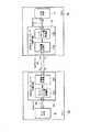
以下、本発明をシリアルATAインタフェース(以下、SATAインタフェースと称する)を持つ磁気ディスクドライブを備えたシステムに適用した一実施形態につき図面を参照して説明する。図1は本発明の一実施形態に係る磁気ディスクドライブ(以下、HDDと称する)10を備えたシステムの構成を示すブロック図である。HDD10は、従来から知られている、ATAインタフェースを用いてパラレルデータ転送を行うHDDの構成であるHDD本体11に加えて、SATAインタフェース制御回路12を備えている。SATAインタフェース制御回路12は、HDD本体11とATAバス(パラレルATAバス)13を介して接続されると共に、ホスト(ホストシステム)20とSATAバス(シリアルATAバス)30を介して接続される周辺機器用のSATAブリッジである。SATAインタフェース制御回路12は、ATAインタフェースとSATAインタフェースとの間のインタフェース変換を行う例えば1チップのLSI(Large Scale Integlated Circuit)である。SATAインタフェース制御回路12は特に、SATAバス30を介して与えられた指示をATAバス13(ATAインタフェース)の信号規則に変換し、当該ATAバス13を介してHDD本体11に送信する機能を有する。 Hereinafter, an embodiment in which the present invention is applied to a system including a magnetic disk drive having a serial ATA interface (hereinafter referred to as a SATA interface) will be described with reference to the drawings. FIG. 1 is a block diagram showing the configuration of a system including a magnetic disk drive (hereinafter referred to as HDD) 10 according to an embodiment of the present invention. The
ホスト20はHDD10を記憶装置として利用する電子機器であり、例えばパーソナルコンピュータである。ホスト20は、従来から知られている、ATAインタフェースを用いてパラレルデータ転送を行うホストの構成であるホスト本体21に加えて、SATAインタフェース制御回路22を備えている。SATAインタフェース制御回路22は、ホスト本体21とATAバス(パラレルATAバス)23を介して接続されると共に、HDD10とSATAバス(シリアルATAバス)30を介して接続される、ATAバス接続のホスト型ブリッジである。SATAインタフェース制御回路22は、HDD10内のSATAインタフェース制御回路12と同様に、ATAインタフェースとSATAインタフェースとの間のインタフェース変換を行う1チップのLSIである。SATAインタフェース制御回路22は特に、ホスト20側のATAバス23を介して与えられた指示をSATAバス30(SATAインタフェース)の信号規則に変換し、当該SATAバス30を介してHDD10に送信する機能を有する。 The
SATAインタフェース制御回路12,22は、それぞれ、物理層処理部121,221と、リンク/トランスポート層処理部122,222とを備えている。物理層処理部121,221は、SATAバス30を介して高速のシリアルデータ転送(送受信)を実行する機能を有する。ここでのデータ転送速度は、1.5Gbps(ギガビット/秒)である。物理層処理部121,221は、SATAバス30から受信した内容を解釈してリンク/トランスポート層処理部122,222(中のリンク層処理部)に伝達する。また物理層処理部121,221は、リンク/トランスポート層処理部122,222(中のリンク層処理部)からの要求に応じてシリアルデータ信号を出力(送信)する。リンク/トランスポート層処理部122,222は、リンク層処理部とトランスポート層処理部(図示せず)とを備えている。リンク層処理部は、トランスポート層処理部からの要求内容に応じて物理層処理部121,221に信号出力の要求を出し、また物理層処理部121,221からの受信入力をトランスポート層処理部へ伝達する。トランスポート層処理部はATAインタフェースとSATAインタフェースとの間のインタフェース変換を行う。 The SATA
なお、ATAバス13,23に代えて、当該ATAバスに準じたバス、例えばPCIバス(Peripheral Component Interconnect Bus)を用いることも可能である。この場合、SATAインタフェース制御回路12,22(を構成するSATAブリッジ)をPCIブリッジ内に設けることが可能である。また、SATAインタフェース制御回路12,22(を構成するSATAブリッジ)には、SATAバス30との間でシリアルATAインタフェースの信号を送受信する機能を持たせれば良い。 In place of the
図2は、図1中のHDD本体11の構成を示すブロック図である。HDD本体11は、記録媒体としてのディスク111を備えている。このディスク111の2つのディスク面の少なくとも一方のディスク面は、データが磁気記録される記録面をなしている。この記録面をなす、ディスク111の一方のディスク面に対応して、ヘッド(磁気ヘッド)112が配置されている。なお、図1では、作図の都合上、ヘッド112が1つであるHDD10の例が示されている。しかし、一般には、ディスク111の2つのディスク面が共に記録面をなしており、各々のディスク面に対応してヘッドが配置される。また図1の構成では、単一枚のディスク111を備えたHDD10を想定している。しかし、ディスク111が複数枚積層配置されたHDDであっても構わない。 FIG. 2 is a block diagram showing a configuration of the HDD
ディスク111はスピンドルモータ(以下、SPMと称する)113により高速に回転させられる。ヘッド112は、ディスク111へのデータ書き込み(データ記録)及びディスク111からのデータ読み出し(データ再生)に用いられる。ヘッド112は、アクチュエータ114の先端に取り付けられている。アクチュエータ114は、当該アクチュエータ114の駆動源となるボイスコイルモータ(以下、VCMと称する)115を有している。アクチュエータ114は、このVCM115により駆動されて、ヘッド112をディスク111の半径方向に移動する。これにより、ヘッド112は、目標トラック上に位置付けられる。SPM113及びVCM115は、モータドライバIC116からそれぞれ供給される駆動電流(SPM電流及びVCM電流)により駆動される。モータドライバIC116は、CPU121から指定された量のSPM電流をSPM113に対して供給する。またモータドライバIC116は、CPU121から指定された量のVCM電流をVCM115に対して供給する。 The
ヘッド112はヘッドIC(ヘッドアンプ回路)117と接続されている。ヘッドIC117はヘッド112により読み出されたリード信号を増幅するリードアンプ、及びライトデータをライト電流に変換するライトアンプを含む。ヘッドIC117は、リード/ライトIC(リード/ライトチャネル)118と接続されている。リード/ライトIC118は、リード信号に対するA/D(アナログ/デジタル)変換処理、ライトデータの符号化処理及びリードデータの復号化処理等の各種の信号処理を実行する信号処理デバイスである。リード/ライトIC118はディスクコントローラ(以下、HDCと称する)119と接続されている。 The head 112 is connected to a head IC (head amplifier circuit) 117. The
HDC119は当該HDC119とディスク111との間のデータ転送を制御するディスク制御機能を有する。HDC119はまた、ATAインタフェースを持つ。即ちHDC119は、ホスト20との間で、ATAバス13を介してコマンド(リード/ライトコマンド等)、及びデータをATAインタフェースにより送受信するATAインタフェース制御機能を有する。但し、HDD10がSATAインタフェースを持つ本実施形態では、HDC119は、従来のHDDとは異なって、ATAバス13を介してSATAインタフェース制御回路12と接続され、当該SATAインタフェース制御回路12及びSATAバス30を介してホスト20と接続されている。HDC119はまた、バッアァRAM120を制御するバッファ制御機能を有する。HDC119は、HDD10の状態をホスト20に通知するためのステータスレジスタ119aを含む。 The
バッファRAM120の記憶領域の一部は、ホスト20とHDD10内のHDC119との間で転送されるデータを一時格納するデータバッファのための領域に用いられる。バッアァRAM120の記憶領域の別の一部は、後述するSATAパワーセーブ不可フラグFを記憶するフラグ記憶領域120aと、受信コマンドの受信時刻を表す時刻情報を記憶するコマンド受信時刻記憶領域120bとに用いられる。コマンド受信時刻記憶領域120bは最新の一定数の受信コマンドの受信時刻情報を記憶するリングバッファとして用いられる。 A part of the storage area of the
CPU130は、制御プログラムが予め格納された図示せぬ不揮発性メモリ(例えば書き換えが可能な不揮発性メモリであるフラッシュROM)を有している。CPU130は、この不揮発性メモリに格納されている制御プログラムに従ってHDD10内の各部を制御する。特にCPU130は、HDC119によって受信されたホスト20からのコマンドがATAインタフェースのパワーセーブモード(以下、ATAパワーセーブモードと称する)を指定する特定コマンド(ATAパワーセーブコマンド)の場合に、HDD10を当該コマンドで指定されたATAパワーセーブモードに設定する。またCPU130は、ATAパワーセーブモードの設定時に、そのモードに予め対応付けられたSATAパワーセーブモードをHDC119、ATAバス13を介してSATAインタフェース制御回路12によって設定させる。 The
図3は、本実施形態で適用されるATAパワーセーブモード(ATAインタフェース規格に準拠したパワーセーブの状態)の状態遷移を示す図である。本実施形態では、ATAパワーセーブモードとして、アクティブ・アイドルモードM1、パフォーマンス・アイドルモードM2、ローパワー・アイドルモードM3、スタンバイモードM4及びスリープモードM5の5種類が用意されている。また、ATAインタフェースのモードとして、これらのパワーセーブ系のモードM1〜M5の他に、リード/ライトコマンドが実行可能なリード/ライトモード(アクティブモード)M0が用意される。ここで、消費電力は、リード/ライトモードM0→アクティブ・アイドルモードM1→パフォーマンス・アイドルモードM2→ローパワー・アイドルモードM3→スタンバイモードM4→スリープモードM5の順に小さくなる。 FIG. 3 is a diagram showing state transitions in the ATA power save mode (power save state compliant with the ATA interface standard) applied in the present embodiment. In this embodiment, five types of ATA power save modes are prepared: an active / idle mode M1, a performance / idle mode M2, a low power / idle mode M3, a standby mode M4, and a sleep mode M5. In addition to these power saving modes M1 to M5, a read / write mode (active mode) M0 capable of executing a read / write command is prepared as an ATA interface mode. Here, the power consumption decreases in the order of read / write mode M0 → active / idle mode M1 → performance / idle mode M2 → low power / idle mode M3 → standby mode M4 → sleep mode M5.
HDD10(内のHDD本体11)では、リード/ライトモードM0におけるリード/ライトコマンドに従うリード/ライトの実行が終了すると、当該HDD10での消費電力の節約のために、CPU130の制御によってアクティブ・アイドルモードM1に遷移させられる。アクティブ・アイドルモードM1に遷移した後一定時間T1が経過してもホスト20から新たなコマンドが送られなかった場合には、当該HDD10での消費電力の一層の節約のために、CPU130の制御によってパフォーマンス・アイドルモードM2に自動的に遷移させられる。モードM1及びM2は、製造者側で任意に規定されたATAパワーセーブモードである。 When the execution of the read / write according to the read / write command in the read / write mode M0 is completed in the HDD 10 (the HDD main body 11), the active / idle mode is controlled by the
パフォーマンス・アイドルモードM2に遷移した後一定時間T2が経過してもホスト20から新たなコマンドが送られなかった場合には、当該HDD10での消費電力の一層の節約のために、CPU130の制御によってローパワー・アイドルモードM3に遷移させられる。このモードM3は、ATAインタフェース規格の“IDLE(アイドル)”に相当する。このため、上記各モードM1,M2においてホスト20からアイドルコマンドが送られた場合、HDD10のATAパワーセーブモードは、当該コマンドに従ってローパワー・アイドルモードM3に遷移される。同様に、上記各モードM1,M2,M3においてホスト20からスタンバイコマンドが送られた場合、HDD10のATAパワーセーブモードは、当該コマンドに従ってスタンバイモードM4に遷移される。なお、スタンバイコマンドの一種に、スタンバイモードに遷移するまでの時間を指定可能なスタンバイ・イミーディエット(Standby Immediate)コマンドが知られている。スタンバイ・イミーディエットコマンドの場合には、当該コマンドで指定された時間後に、スタンバイモードM4に遷移される。また、上記各モードM1,M2,M3,M4においてホスト20からスリープコマンドが送られた場合、HDD10のATAパワーセーブモードは、当該コマンドに従ってスリープモードM5に遷移される。また、上記各モードM1,M2,M3,M4,M5においてホスト20からリード/ライトコマンドが送られた場合、HDD10のATAパワーセーブモードは、当該コマンドに従ってリード/ライトモードM0に遷移される。 If a new command is not sent from the
図4は、上記各モードM0〜M5と当該モードM0〜M5におけるHDD本体11内の各回路の電源OFF状態との対応関係を示す。リード/ライトモードM0では、HDD本体11内の各回路に、当該HDD本体11にてリード/ライト動作を即時に実行できるように電源が供給される。アクティブ・アイドルモードM1、パフォーマンス・アイドルモードM2及びローパワー・アイドルモードM3の各アイドルモードでは、HDD本体11内の一部の回路への電源供給が遮断(OFF)される。アクティブ・アイドルモードM1では、ディスク111はSPM113により回転されており、ヘッド112は、サーボ制御によりディスク111上のあるトラックに位置決めされている。パフォーマンス・アイドルモードM2では、ディスク111はSPM113により回転されており、ヘッド112はサーボ制御されずにディスク111上の任意のトラック上に存在する。ローパワー・アイドルモードM3では、ディスク111はSPM113により回転されているが、ヘッド112はディスク111から外れた退避箇所に移動されている。このためアクティブ・アイドルモードM1ではリード/ライトIC118内の一部の回路(ライトチャネル)への電源供給だけが遮断される。これに対し、パフォーマンス・アイドルモードM2ではモータドライバIC116内の一部の回路(VCMドライバ)及びリード/ライトIC118内の一部の回路への電源供給が遮断される。また、ローパワー・アイドルモードM3では、モータドライバIC116内の一部の回路への電源供給が遮断されると共に、ヘッドIC117及びリード/ライトIC118への電源供給が遮断される。リード/ライトモードM0に復帰するまでの時間(つまり、リード/ライトを再び実行可能とするまでの復帰時間)は、上記各アイドルモードによって異なり、アクティブ・アイドルモードM1→パフォーマンス・アイドルモードM2→ローパワー・アイドルモードM3の順に長くなる。上記各アイドルモードで必要となる消費電力は、アクティブ・アイドルモードM1→パフォーマンス・アイドルモードM2→ローパワー・アイドルモードM3の順に小さくなり、復帰時間が長い方が小さい。 FIG. 4 shows a correspondence relationship between the respective modes M0 to M5 and the power OFF state of each circuit in the HDD
スタンバイモードM4では、SPM113の回転は停止される。ここでは、SPM113、モータドライバIC116、ヘッドIC117、リード/ライトIC118及びバッアァRAM120への電源供給が遮断される。このため、スタンバイモードM4での消費電力は、ローパワー・アイドルモードM3よりも更に小さくなり、逆に復帰時間は長くなる。 In the standby mode M4, the rotation of the
スリープモードM5では、HDC119内の一部の回路(リセット処理回路)だけに電源が供給されるだけで、殆どの回路への電源供給が遮断される。ここでは、リード/ライトモードM0への復帰はリセット動作によってのみ可能であり、復帰時間はスタンバイモードM4から復帰する場合と同程度である。スリープモードM5における消費電力は、上記各モードM0〜M5の中で最も小さい。 In the sleep mode M5, power is supplied only to a part of the circuits (reset processing circuit) in the
図5は、上記各モードM1〜M5からリード/ライトモードM0に復帰するのに要する時間の一例を示す。 FIG. 5 shows an example of the time required to return from the above modes M1 to M5 to the read / write mode M0.
図6は、上記モードM0〜M5と、HDD10が当該モードM0〜M5に設定された場合に、当該HDD10内のCPU130の制御によって設定されるSATAパワーセーブモードとの関係を示す。図6の例では、ATAパワーセーブモード(ATAインタフェースモード)がリード/ライトモードM0の場合、SATAパワーセーブモード(SATAインタフェースモード)はアイドル(Idle)モードM11に設定される。また、ATAパワーセーブモードがアクティブ・アイドルモードM1またはパフォーマンス・アイドルモードM2の場合、SATAパワーセーブモードはパーシャル(Partial)モードM12に設定される。但し、パフォーマンス・アイドルモードM2はアクティブ・アイドルモードM1からしか遷移しないため、パフォーマンス・アイドルモードM2への遷移時には、パーシャルモードM12が継続されることになる。また、ATAパワーセーブモードがローパワー・アイドルモードM3、スタンバイモードM4またはスリープモードM5の場合、SATAパワーセーブモードはスランバ(Slumber)モードM13に設定される。 FIG. 6 shows the relationship between the modes M0 to M5 and the SATA power save mode set by the control of the
次に、図1のシステムにおける動作を、HDD10内のHDD本体11においてホスト20からのコマンドを受信した場合に行われるパワー制御を例に、図7のフローチャートを参照して説明する。 Next, operations in the system of FIG. 1 will be described with reference to the flowchart of FIG. 7 by taking as an example power control performed when a command from the
今、ホスト20のホスト本体21からATAバス23にATAインタフェース規格に準拠したHDD10宛てのコマンドが送出されたものとする。このATAバス23上のコマンドはホスト20のSATAインタフェース制御回路22で受信される。SATAインタフェース制御回路22のリンク/トランスポート層処理部222は、受信コマンドをSATAインタフェース規格に準拠したコマンド(SATAバス30の信号規則)に変換してSATAバス30に送出する。このSATAバス30上のコマンドはHDD10のSATAインタフェース制御回路12で受信される。SATAインタフェース制御回路12のリンク/トランスポート層処理部122は、受信コマンドをATAインタフェース規格に準拠したコマンド(ATAバス13の信号規則)に変換してATAバス13に送出する。このATAバス13上のコマンドはHDD10のHDD本体11に設けられたHDC119で受信される。HDC119からは、SATAインタフェース制御回路12がホストとして認識される。HDC119によって受信されたコマンドはCPU130に渡される。 Assume that a command addressed to the
CPU130は、HDC119から渡されたコマンドを受け取ると、当該コマンドの受信時刻を表すコマンド受信時刻情報をバッアァRAM120内のコマンド受信時刻記憶領域120bに格納する(ステップS1)。次にCPU130は、受信コマンドが予め定められたコマンドの1つであるか否かを判定する(ステップS2)。ここで、予め定められたコマンドは、パワーセーブに関係するコマンドであり、アイドルコマンド、スタンバイコマンド、及びスリープコマンドである。 When receiving the command passed from the
受信コマンドが予め定められたコマンドの1つである場合、CPU130は以下に述べる処理を実行する。まずCPU130は、受信コマンドを解釈して当該コマンドの指示する動作を実行する(ステップS3)。つまり、受信コマンドがアイドルコマンドである場合、CPU130はHDD10のATAパワーセーブモードをローパワー・アイドルモードM3に遷移させる。また、受信コマンドがスタンバイコマンドである場合、CPU130はHDD10のATAパワーセーブモードをスタンバイモードM4に遷移させる。また、受信コマンドがスリープコマンドである場合、CPU130はHDD10のATAパワーセーブモードをスリープモードM5に遷移させる。 When the received command is one of predetermined commands, the
CPU130は、受信コマンドを実行し終えて、当該コマンドの実行完了を確認すると、当該コマンドの実行完了をホスト20に報告するための処理を行う(ステップS4)。即ちCPU130は、コマンド実行完了を示す応答ステータスをステータスレジスタ119aに設定して、ATAバス13に割り込み信号を送出する。SATAインタフェース制御回路12は、この割り込み信号に応じて、HDC119内のステータスレジスタ119aの内容をリードする。SATAインタフェース制御回路12は、リードしたステータスレジスタ119aの内容をもとに、SATAインタフェース規格に準拠したコマンド実行完了報告をSATAバス30を介してホスト20に送出する。ホスト20内のSATAインタフェース制御回路22は、SATAバス30上のコマンド実行完了報告を受信すると、ホスト本体21に対してATAバス23を介して割り込み信号を送出する。ホスト本体21は、この割り込み信号に応じてSATAインタフェース制御回路22からコマンド実行完了報告(コマンド完了応答)を受け取る。 When
さて本実施形態では、ホスト20からHDD10に送られたコマンドが、予め定められたコマンド、即ちパワーセーブに関係するコマンドの1つである場合、CPU130はSATAインタフェース制御回路12に対し、SATAパワーセーブモードの制御(つまりATAバス13のパワー制御)を実行する。ここでは、アイドルコマンド、スタンバイコマンド、またはスリープコマンドの場合、いずれもスランバモードM13に遷移するように制御される。 In this embodiment, when the command sent from the
CPU130によるSATAパワーセーブモードの制御は、SATAインタフェース規格に準拠したSATAパワーセーブモードを指定する信号パターンが設定されたプリミティブをATAバス13を介してSATAインタフェース制御回路12のリンク/トランスポート層処理部122(に含まれているリンク処理部)に送信することにより実現される。なお、SATAインタフェース制御回路12内にSATAパワーセーブモードの制御のための制御レジスタを設け、当該レジスタをCPU130から制御することにより、SATAバス30を目的のSATAパワーセーブモードに遷移させても良い。 The control of the SATA power save mode by the
本実施形態では以下に示す理由により、ATAパワーセーブに関係するコマンドの実行完了の報告(コマンド完了応答)後、対応するSATAパワーセーブモードに直ちに遷移させる構成を適用していない。まず、コマンド実行完了報告後に、SATAバス30を即時にスランバモードM13に遷移させると、当該スランバモードM13の定義から、コマンドの応答に対して最大10msの復帰時間を要する。ここで、ホスト20がスタンバイコマンド、例えばスタンバイ・イミーディエットコマンドをHDD10に対して発行し、しかる後にチェックパワーモードコマンドを用いてHDD10内のSPM113の停止を確実に監視しようという場合を想定する。この場合、スタンバイ・イミーディエットコマンドの実行完了報告(コマンド完了応答)後、SATAパワーセーブモードを即時にスランバモードM13に移行してしまうと、引き続くチェックパワーモードコマンドに対する完了応答の速度が低下してしまう。このため本実施形態では、コマンド完了応答後にSATAバス30を無条件で即時にスランバモードM13に遷移させることはしない。 In the present embodiment, for the reason described below, a configuration in which a transition to a corresponding SATA power save mode is immediately performed after a command execution completion report (command completion response) related to ATA power save is not applied. First, when the
このことについて、更に詳細に説明する。まず、スタンバイ・イミーディエットコマンドの終了時点で即時にスランバモードM13に遷移した場合に、その直後にホスト20がHDD10に対してチェックパワーモードコマンドを発行したものとする。この場合、チェックパワーモードコマンドの発行時点には、SATAバス30は既にスランバモードM13移行している。この状態でSATAバス30を通してホスト20からHDD10のHDC119にコマンドが伝達されるためには、当該SATAバス30が通信可能な状態、つまりアイドルモードM11に復帰されなければならない。このとき、ホスト20内のSATAインタフェース制御回路22では、チェックパワーモードコマンドに応じて、SATAインタフェースの状態遷移規則に従って復帰手順が実施される。この場合、ホスト20では、チェックパワーモードコマンドの完了応答が、SATAバス30の復帰時間だけ遅くなったように認識される。 This will be described in more detail. First, assume that the
さて、ホスト20から発行されたコマンド(チェックパワーモードコマンド)は、当該コマンドの発行に応じて、SATAバス30の状態がスランバモードM13(パワーセーブ状態)からアイドルモードM11に復帰し、ホスト20とHDD10との間の交信が可能となった後にHDD10に到達する。そして、SATAインタフェース制御回路12のリンク/トランスポート層処理部122(に含まれているトランスポート層処理部)が作動して、HDD10内のHDC119に対してコマンドを発行する。このため、ホスト20から発行されたコマンドは、SATAバス30の復帰時間だけ遅れてHDD10内のHDC119に到達する。しかし、HDC119は、その遅れを認識できない。 The command (check power mode command) issued from the
そこで本実施形態では、HDD10内のCPU130は、SATAパワーセーブモードを制御しようとする場合、まずバッアァRAM120のコマンド受信時刻記憶領域120bに記憶されているコマンド受信時刻情報の示す例えば一定個数のコマンド受信時刻の系列から、コマンドの受信頻度を算出する(ステップS7)。ここで、コマンド受信頻度には、例えばコマンド受信時刻系列で示されるコマンド受信時間間隔の平均値、或いは最も確率の高いコマンド受信時間間隔を用いることができる。なお、一定個数のコマンド受信時刻の系列に代えて、現在時刻を基準とする一定時間内に受信されたコマンド受信時刻の系列を用いても構わない。 Therefore, in this embodiment, when the
CPU130は、算出されたコマンド受信頻度(コマンド受信時間間隔)から、今回受信したコマンドで決まるSATAパワーセーブモードに遷移するタイミングを決定し、そのタイミングが到来するのを待って、当該SATAパワーセーブモードへの遷移を制御する(ステップS8)。ここでは、算出されたコマンド受信頻度、つまりコマンド受信時間間隔をTcとすると、CPU130は時間Tcを待っても次のコマンドがHDC119で受信されなかった場合に、SATAバス30を、今回受信したコマンドで決まるSATAパワーセーブモードにSATAインタフェース制御回路12によって遷移させる(ステップS9)。これにより、ATAパワーセーブ系のコマンドの実行時に、当該コマンドで決まるSATAパワーセーブモードへの遷移を制御しても、ホスト20から次のコマンドが送られた場合に、当該次のコマンドに対する完了応答が遅れることを防止できる。 The
なお、ATAパワーセーブ系のコマンドの後にホスト20からHDD10にチェックパワーモードコマンドが発行される可能性が高いことを考慮して、ATAパワーセーブ系のコマンドの完了応答後に、CPU130がSPM113の停止状態を確認し、その確認時点から予め定められた一定時間後にスランバモードM13への遷移を制御するようにしても、次のコマンドに対する完了応答が遅れることを防止できる。また、SPM113の再起動を必要としないコマンドを最も最近に受信した時点から一定時間後にスランバモードM13への遷移を制御するようにしても良い。また本実施形態では、ホスト20からのATAパワーセーブ系のコマンドが、アイドルコマンド、スタンバイコマンドコマンドまたはスリープコマンドのいずれの場合にも、SATAパワーセーブモードをスランバモードM13としている。しかし、コマンドの種類、或いはSATAインタフェース制御回路12の構成(アイドルモードM11に復帰する能力)によっては、より短時間で復帰できるパーシャルモードM12に遷移するようにしても良い。 In consideration of the high possibility that the
さて本実施形態では、HDD10における消費電力を低減するために、図3に示すように、ホスト20からのATAパワーセーブ系のコマンドとは別に、HDD10内部で自律的にATAパワーセーブモードの遷移が行われる構成が適用されている。つまり、HDD10内のCPU130は、リード/ライトモードM0でのリード/ライト実行が終了すると、直ちにリード/ライトモードM0からアクティブ・アイドルモードM1に遷移させる。またアクティブ・アイドルモードM1への遷移後、一定時間T1を経過してもホスト20から新たなコマンドが送られなかった場合には、HDD10内のCPU130はアクティブ・アイドルモードM1からパフォーマンス・アイドルモードM2に遷移させる。またパフォーマンス・アイドルモードM2への遷移後、一定時間T2を経過してもホスト20から新たなコマンドが送られなかった場合には、CPU130はパフォーマンス・アイドルモードM2からローパワー・アイドルモードM3に遷移させる。ここで、上記時間T1,T2を、先に述べたコマンド受信頻度(コマンド受信時間間隔)から、例えば一定周期で動的に変更すると良い。 In the present embodiment, in order to reduce the power consumption in the
本実施形態では、このHDD10内部でのCPU130の制御による自律的なATAパワーセーブモードの遷移時に、図3に示すように、その遷移に連動してSATAパワーセーブモードも遷移させている。具体的には、リード/ライトモードM0からアクティブ・アイドルモードM1への遷移時に、アイドルモードM11からパーシャルモードM12に遷移される。また、アクティブ・アイドルモードM1からパフォーマンス・アイドルモードM2に遷移した場合には、パーシャルモードM12が継続される。また、パフォーマンス・アイドルモードM2からローパワー・アイドルモードM3の遷移時には、パーシャルモードM12からスランバモードM13に遷移される。ローパワー・アイドルモードM3では、ヘッド112はディスク111から外れた退避箇所に移動される。HDD10が、この状態になると、その後ホスト20からリード/ライトコマンドが与えられた場合に、リード/ライトモードM0に復帰するにのに要する時間は30ms以上(図6参照)と比較的長い。そこで、このような場合に、本実施形態のようにSATAバス30をスランバモードM13に設定してSATAバス30(SATAインタフェース)での消費電力を抑えることは有効である。 In this embodiment, at the time of transition of the autonomous ATA power save mode under the control of the
ホスト20からHDD10へのアクセスは時系列的に集中、或いは分散の傾向がある。例えばコマンド受信時間間隔が非常に短い状態が続いた後に、一定時間を超えてコマンドが受信されないことがある。このような場合、CPU130が、ホスト20におけるアプリケーションの実行が終了したものと推定して、比較的短時間で消費電力を下げるATAパワーセーブモードに設定すると良い。また、コマンド受信時間間隔は比較的長いものの、その状態が長時間続く場合、つまり継続してHDD10がアクセスされる場合には、CPU130が消費電力を下げる状態にするまでの時間が比較的長いATAパワーセーブモードに設定すると良い。ここでも、これらのSATAパワーセーブモードと連動してSATAパワーセーブモードを制御すると良い。 Access from the
また、本実施形態では、SATAパワーセーブモード(SATAバス30のパワーセーブ)がHDD10内のCPU130によって制御される。しかし、この制御が、SATAインタフェース制御回路12によって行われる構成とすることも可能である。図8は、SATAインタフェース制御回路12によってSATAパワーセーブモードが制御される場合の状態遷移を示す。今、ホスト20からのコマンドがSATAインタフェース制御回路12で受信された結果、SATAバス30がアイドルモードM11に遷移(復帰)したものとする。このアイドルモードM11への遷移時点から一定時間Tを経過しても新たなコマンドがホスト20から送られなかった場合、SATAインタフェース制御回路12は、SATAバス30をアイドルモードM11からパーシャルモードM12に遷移させる制御を行う。このパーシャルモードM12への遷移時点から一定時間Tを経過しても新たなコマンドがホスト20から送られなかった場合、SATAインタフェース制御回路12は、SATAバス30をパーシャルモードM12からスランバモードM13に遷移させる制御を行う。このスランバモードM13は、新たなコマンドがホスト20から送られるまで継続される。ここで、一定時間Tは、タイマ(時間計測手段)を用いて計測すれば良い。なお、アイドルモードM11からパーシャルモードM12に遷移した場合、新たなコマンドがホスト20から送られるまで当該パーシャルモードM12が継続される構成としても良い。またアイドルモードM11から直接スランバモードM13に遷移させる構成とすることも可能である。また、このSATAインタフェース制御回路12によるSATAパワーセーブモード制御機能を、HDD10内のHDC119に持たせることも可能である。 In this embodiment, the SATA power save mode (power save of the SATA bus 30) is controlled by the
本実施形態では、SATAパワーセーブモードの制御(SATAバス30のパワーセーブ)がHDD10側から(つまりHDD10の主導により)行われる。このSATAパワーセーブモードの制御のためには、HDD10側のSATAインタフェース制御回路12だけでなく、ホスト20側のSATAインタフェース制御回路22も共にSATAパワーセーブモードに対応していること(つまりSATAパワーセーブ機能をサポートしていること)が必要となる。もし、SATAインタフェース制御回路22がSATAパワーセーブモード(パーシャルモードM12及びスランバモードM13の各モード)に対応していない場合、指示されたSATAパワーセーブモードへの遷移は不可能となる。この状態については、SATAバスにより相互接続されたSATAインタフェース制御回路(本実施形態では、SATAインタフェース制御回路12及び22)相互の動作で知ることができる方法が、SATAインタフェース規格で定義されている。今、HDD10がSATAバス30を介して接続されているホスト20が、スランバモードM13に対応していない(SATAインタフェース制御回路22を含む)ものとする。この場合、HDD10側からスランバモードM13への移行指示(を表すパターンを含むプリミティブ)がホスト20に発行される都度、当該ホスト20(内のSATAインタフェース制御回路22)からはスランバモードM13への移行不能の応答が返される。このように、HDD10がSATAバス30を介して接続されているホスト20がSATAパワーセーブモードに対応していない場合、HDD10側からホスト20に対してSATAパワーセーブモードへの移行指示を発行しても、ホスト20からは常に移行不能の応答が返されるだけであり、SATAパワーセーブモードの制御は失敗する。つまり、HDD10がSATAパワーセーブモードに対応していないホスト20とSATAバス30を介して接続されている場合、HDD10がSATAパワーセーブモードの制御を実行することは無駄である。 In the present embodiment, control of the SATA power save mode (power save of the SATA bus 30) is performed from the
そこで本実施形態では、ホスト20から指示されたSATAパワーセーブモードへの移行不能の応答が返された場合、つまりSATAパワーセーブモードの制御に失敗した場合、HDD10内のCPU130は、バッアァRAM120内のフラグ記憶領域120aに記憶されているSATAパワーセーブ不可フラグFをON状態にする(ステップS9,S10)。これにより、次にSATAパワーセーブモードの制御が必要となった場合、CPU130はSATAパワーセーブ不可フラグFの状態を参照することで、SATAパワーセーブが不可であるか否かを判定することができる(ステップS5,S6)。SATAパワーセーブ不可フラグFがON状態にある場合、CPU130はSATAパワーセーブが不可であると判定する。この場合、CPU130はSATAパワーセーブモードの制御の実行(ステップS7,S8)を控える。これにより、ホスト20のSATAインタフェース制御回路22がSATAパワーセーブモードに対応していないにも拘わらずに、不要なSATAパワーセーブモードの状態遷移のための制御が行われることを防止でき、シリアルATAバス30の動作を安定させることができる。 Therefore, in the present embodiment, when the response indicating that the
HDD10及びホスト20の双方がSATAパワーセーブモードに対応している場合、ホスト20側から(つまりホスト20の主導により)SATAパワーセーブモードを制御することも可能である。しかし、HDD10内では、ホスト20からのATAパワーセーブ系のコマンドとは別に自律的にATAパワーセーブモードへの状態遷移が行われている。したがって、このHDD10内のATAパワーセーブモードに無関係にホスト20側からSATAバス30のSATAパワーセーブモードを制御するよりも、上記実施形態のようにHDD10内のATAパワーセーブモードに連動させてHDD10側からSATAバス30のSATAパワーセーブモードを制御する方が、HDD10内のATAパワーセーブモードに適したSATAパワーセーブモードを設定することができる。 When both the
上記実施形態では、本発明をHDD(磁気ディスクドライブ)を備えたシステムに適用した場合について説明した。しかし本発明は、光ディスクドライブ、光磁気ディスクドライブなどHDD以外のディスクドライブを備えたシステム、更にはディスクドライブ以外の電子機器を備えたシステムでも、SATAインタフェースを持つ電子機器を備えたシステムであれば、適用可能である。 In the above embodiment, the case where the present invention is applied to a system including an HDD (magnetic disk drive) has been described. However, the present invention is not limited to a system having a disk drive other than an HDD such as an optical disk drive or a magneto-optical disk drive, or even a system having an electronic device other than a disk drive, as long as the system has an electronic device having a SATA interface. Applicable.
なお、本発明は、上記実施形態そのままに限定されるものではなく、実施段階ではその要旨を逸脱しない範囲で構成要素を変形して具体化できる。また、上記実施形態に開示されている複数の構成要素の適宜な組み合せにより種々の発明を形成できる。例えば、実施形態に示される全構成要素から幾つかの構成要素を削除してもよい。 Note that the present invention is not limited to the above-described embodiment as it is, and can be embodied by modifying the constituent elements without departing from the scope of the invention in the implementation stage. Further, various inventions can be formed by appropriately combining a plurality of constituent elements disclosed in the embodiment. For example, some components may be deleted from all the components shown in the embodiment.
10…HDD(磁気ディスクドライブ、電子機器)、11…HDD本体、12,22…SATAインタフェース制御回路(シリアルATAインタフェース制御回路)、13,23…ATAバス、20…ホスト、21…ホスト本体、30…SATAバス(シリアルATAバス)、111…ディスク、112…ヘッド、113…SPM(スピンドルモータ)、116…モータドライバ、117…ヘッドIC、118…リード/ライトIC、119…HDC(ディスクコントローラ)、119a…ステータスレジスタ、120…バッアァRAM、120a…フラグ記憶領域、120b…コマンド受信時刻記憶領域、130…CPU。 DESCRIPTION OF
Claims (11)
Translated fromJapaneseホストから出力された電子機器を第1のパワーセーブモードに設定することを指定するコマンドを受信する受信手段と、
前記コマンドの受信の後、前記第1のパワーセーブモードに対応付けられたシリアルATAインタフェースの第2のパワーセーブモードの設定を制御する制御手段と
を具備することを特徴とするシリアルATAインタフェースを持つ電子機器。In an electronic device having a serial ATA interface connected to a host via a serial ATA bus,
Receiving means for receiving a command designating setting of the electronic device output from the host to the first power save mode;
And a control means for controlling the setting of the second power save mode of the serial ATA interface associated with the first power save mode after receiving the command. Electronics.
前記第2のパワーセーブモードがスランバモードまたはパーシャルモードである
ことを特徴とする請求項1記載のシリアルATAインタフェースを持つ電子機器。The command specifying the first power save mode is a sleep command, a standby command or an idle command defined by the ATA interface standard,
Electronic device with serial ATA interface of claim1, wherein the second power save mode is scan lamba mode or the partial mode.
前記検出結果を示すフラグ情報を記憶する手段とを更に具備し、
前記制御手段は、前記制御の前に前記フラグ情報を参照し、当該フラグ情報により前記ホスト側が前記シリアルATAインタフェースのパワーセーブ機能をサポートしていないことが検出された場合、前記制御を控えることを特徴とする請求項1記載のシリアルATAインタフェースを持つ電子機器。Means for detecting whether the host side supports a power saving function of a serial ATA interface based on the control by the control means;
Means for storing flag information indicating the detection result;
The control means refers to the flag information before the control, and refrains from the control when it is detected from the flag information that the host side does not support the power saving function of the serial ATA interface. The electronic device having a serial ATA interface according to claim1 .
前記計測手段により前記一定時間が計測されているときに前記ホストからのコマンドが受信されなかった場合に、前記シリアルATAインタフェースを、前記アイドルモードまたはパーシャルモードから、それぞれパーシャルモードまたはスランバモードに移行する移行手段と
を更に具備することを特徴とする請求項1記載のシリアルATAインタフェースを持つ電子機器。Measuring means for starting time measurement for measuring a predetermined time each time the serial ATA interface shifts to the idle mode or the partial mode which is one of the power saving modes;
The serial ATA interface is shifted from the idle mode or the partial mode to the partial mode or the slumber mode when the command from the host is not received when the predetermined time is measured by the measuring means. electronic device with serial ATA interface of claim1, wherein the further comprising a shifting unit for.
ことを特徴とする請求項1乃至4のいずれかに記載のシリアルATAインタフェースを持つ電子機器。The electronic device is an electronic device with a serial ATA interface as claimed in any of claims 1 to4, characterized in that it comprises a disk drive.
ホストから出力された電子機器を第1のパワーセーブモードに設定することを指定するコマンドを受信する受信手段と、
前記コマンドの受信の後、前記第1のパワーセーブモードに対応付けられたシリアルATAインタフェースの第2のパワーセーブモードの設定を制御する制御手段と
を具備することを特徴とするコントローラ。In a controller provided in an electronic device having a serial ATA interface connected to a host via a serial ATA bus,
Receiving means for receiving a command designating setting of the electronic device output from the host to the first power save mode;
And a controller that controls setting of the second power save mode of the serial ATA interface associated with the first power save mode after receiving the command.
前記第2のパワーセーブモードがスランバモードまたはパーシャルモードである
ことを特徴とする請求項6記載のコントローラ。The command specifying the first power save mode is a sleep command, a standby command or an idle command defined by the ATA interface standard,
The controller according to claim6, wherein the second power save mode is a slumber mode or a partial mode.
前記電子機器を利用するホストと、
前記電子機器と前記ホストが接続されるシリアルATAバスと
を具備することを特徴とする情報機器。An electronicequipment according to claim1,
A host using the electronic device;
An information device comprising: the electronic device and a serial ATA bus to which the host is connected.
前記第2のパワーセーブモードがスランバモードまたはパーシャルモードである
ことを特徴とする請求項8記載の情報機器。The command specifying the first power save mode is a sleep command, a standby command or an idle command defined by the ATA interface standard,
The information device according to claim8, wherein the second power save mode is a slumber mode or a partial mode.
ホストから出力された電子機器を第1のパワーセーブモードに設定することを指定するコマンドを受信するステップと、
前記コマンドの受信の後、前記第1のパワーセーブモードに対応付けられたシリアルATAインタフェースの第2のパワーセーブモードを設定するステップと
を具備することを特徴とするシリアルATAバスのパワーセーブ方法。A power saving method of a serial ATA bus in an electronic device having a serial ATA interface connected to a host via a serial ATA bus,
Receiving a command specifying that the electronic device output from the host is set to the first power save mode;
After the command is received, the method further comprises the step of: setting a second power save mode of the serial ATA interface associated with the first power save mode.
前記第2のパワーセーブモードがスランバモードまたはパーシャルモードである
ことを特徴とする請求項10記載のシリアルATAバスのパワーセーブ方法。The command specifying the first power save mode is a sleep command, a standby command or an idle command defined by the ATA interface standard,
The serial ATA bus power saving method according to claim10, wherein the second power saving mode is a slumber mode or a partial mode.
Priority Applications (18)
| Application Number | Priority Date | Filing Date | Title |
|---|---|---|---|
| JP2003310361AJP4371739B2 (en) | 2003-09-02 | 2003-09-02 | Electronic device having serial ATA interface and power saving method of serial ATA bus |
| SG200503835ASG113619A1 (en) | 2003-09-02 | 2004-08-20 | Electronic device with serial ata interface and power saving method for serial ata buses |
| SG200404527ASG109565A1 (en) | 2003-09-02 | 2004-08-20 | Electronic device with serial ata interface and power saving method for serial ata buses |
| US10/931,949US7328356B2 (en) | 2003-09-02 | 2004-09-01 | Apparatus and method for saving power in a disk drive with a serial ATA interface connected to a host via a serial ATA bus |
| CNB200410068692XACN1296799C (en) | 2003-09-02 | 2004-09-02 | Electronic device with serial ATA interface and power saving method for serial ATA buses |
| US11/956,996US7747885B2 (en) | 2003-09-02 | 2007-12-14 | Electronic device with serial ATA interface and power saving method for serial ATA buses |
| US12/398,569US7856565B2 (en) | 2003-09-02 | 2009-03-05 | Electronic device with serial ATA interface and power saving method for serial ATA buses |
| US12/398,499US7797562B2 (en) | 2003-09-02 | 2009-03-05 | Electronic device with serial ATA interface and power saving method for serial ATA buses |
| US12/398,530US20090172312A1 (en) | 2003-09-02 | 2009-03-05 | Electronic device with serial ata interface and power saving method for serial ata buses |
| US12/398,513US8219837B2 (en) | 2003-09-02 | 2009-03-05 | Electronic device and power saving method using predetermined command to designate portion of device in power saving mode |
| US12/398,556US7882378B2 (en) | 2003-09-02 | 2009-03-05 | Electronic device with serial ATA interface and power saving method for serial ATA buses |
| US12/398,585US7770041B2 (en) | 2003-09-02 | 2009-03-05 | Electronic device with serial ATA interface and power saving method for serial ATA buses |
| US12/398,576US7856567B2 (en) | 2003-09-02 | 2009-03-05 | Electronic device with serial ATA interface and power saving method for serial ATA buses |
| US12/398,544US7809967B2 (en) | 2003-09-02 | 2009-03-05 | Electronic device with serial ATA interface and power saving method for serial ATA buses |
| US12/398,524US20090177905A1 (en) | 2003-09-02 | 2009-03-05 | Electronic device with serial ata interface and power saving method for serial ata buses |
| US12/879,332US8732502B2 (en) | 2003-09-02 | 2010-09-10 | Electronic device with serial ATA interface and power saving method for serial ATA buses |
| US15/160,846USRE47050E1 (en) | 2003-09-02 | 2016-05-20 | Electronic device with serial ATA interference and power saving method for serial ATA buses |
| US15/837,317USRE48190E1 (en) | 2003-09-02 | 2017-12-11 | Electronic device with serial ATA interface and power saving method for serial ATA buses |
Applications Claiming Priority (1)
| Application Number | Priority Date | Filing Date | Title |
|---|---|---|---|
| JP2003310361AJP4371739B2 (en) | 2003-09-02 | 2003-09-02 | Electronic device having serial ATA interface and power saving method of serial ATA bus |
Related Child Applications (10)
| Application Number | Title | Priority Date | Filing Date |
|---|---|---|---|
| JP2008248669ADivisionJP4327893B2 (en) | 2008-09-26 | 2008-09-26 | Electronic equipment with serial ATA interface |
| JP2009009230ADivisionJP4435260B2 (en) | 2009-01-19 | 2009-01-19 | Electronic equipment with serial ATA interface |
| JP2009009231ADivisionJP4405577B2 (en) | 2009-01-19 | 2009-01-19 | Electronic equipment with serial ATA interface |
| JP2009009226ADivisionJP4410298B2 (en) | 2009-01-19 | 2009-01-19 | Electronic equipment with serial ATA interface |
| JP2009009224ADivisionJP4374070B2 (en) | 2009-01-19 | 2009-01-19 | Electronic equipment with serial ATA interface |
| JP2009009227ADivisionJP4352099B2 (en) | 2009-01-19 | 2009-01-19 | Electronic equipment with serial ATA interface |
| JP2009009228ADivisionJP4352100B2 (en) | 2009-01-19 | 2009-01-19 | Electronic equipment with serial ATA interface |
| JP2009009232ADivisionJP4405578B2 (en) | 2009-01-19 | 2009-01-19 | Electronic equipment with serial ATA interface |
| JP2009009229ADivisionJP4405576B2 (en) | 2009-01-19 | 2009-01-19 | Electronic equipment with serial ATA interface |
| JP2009009225ADivisionJP2009080856A (en) | 2009-01-19 | 2009-01-19 | Electronic equipment with serial ATA interface |
Publications (2)
| Publication Number | Publication Date |
|---|---|
| JP2005078514A JP2005078514A (en) | 2005-03-24 |
| JP4371739B2true JP4371739B2 (en) | 2009-11-25 |
Family
ID=34412255
Family Applications (1)
| Application Number | Title | Priority Date | Filing Date |
|---|---|---|---|
| JP2003310361AExpired - LifetimeJP4371739B2 (en) | 2003-09-02 | 2003-09-02 | Electronic device having serial ATA interface and power saving method of serial ATA bus |
Country Status (4)
| Country | Link |
|---|---|
| US (14) | US7328356B2 (en) |
| JP (1) | JP4371739B2 (en) |
| CN (1) | CN1296799C (en) |
| SG (2) | SG113619A1 (en) |
Families Citing this family (121)
| Publication number | Priority date | Publication date | Assignee | Title |
|---|---|---|---|---|
| US7885282B2 (en)* | 2003-07-24 | 2011-02-08 | Seagate Technology Llc | Dynamic control of physical layer quality on a serial bus |
| JP4371739B2 (en) | 2003-09-02 | 2009-11-25 | 株式会社東芝 | Electronic device having serial ATA interface and power saving method of serial ATA bus |
| US20050138441A1 (en)* | 2003-12-19 | 2005-06-23 | Huffman Amber D. | Power management without interrupt latency |
| US7783802B1 (en)* | 2004-02-09 | 2010-08-24 | Lsi Corporation | Serial advanced technology attachment (SATA) switch that toggles with power control to hard disk drive while avolding interruption to system |
| JP2005339135A (en)* | 2004-05-26 | 2005-12-08 | Toshiba Corp | Electronic device having serial ATA interface and power saving control method in the same device |
| US20060069930A1 (en)* | 2004-09-30 | 2006-03-30 | Seagate Technology Llc | Bus architecture with reduced power mode during an access time |
| JP2006099665A (en)* | 2004-09-30 | 2006-04-13 | Hitachi Global Storage Technologies Netherlands Bv | Data storage device and method for controlling power save mode of serial interface portion thereof |
| CN100555173C (en)* | 2004-10-22 | 2009-10-28 | 松下电器产业株式会社 | External memory and method for managing power supply thereof |
| JP2006139459A (en)* | 2004-11-11 | 2006-06-01 | Hitachi Global Storage Technologies Netherlands Bv | Media drive and power saving method thereof |
| JP2006164012A (en)* | 2004-12-09 | 2006-06-22 | Hitachi Global Storage Technologies Netherlands Bv | Data storage device and power save mode control method thereof |
| JP4295204B2 (en)* | 2004-12-16 | 2009-07-15 | インターナショナル・ビジネス・マシーンズ・コーポレーション | Magnetic disk device power control method, program, power control device, and electronic information device |
| JP2007012136A (en)* | 2005-06-29 | 2007-01-18 | Toshiba Corp | Video display device and recording / reproducing control method of recording medium |
| JP2007026125A (en)* | 2005-07-19 | 2007-02-01 | Hitachi Ltd | Recording / playback device |
| JP2007034537A (en) | 2005-07-25 | 2007-02-08 | Sony Corp | Composite storage device, data writing method, and program |
| KR101205324B1 (en) | 2005-11-25 | 2012-11-28 | 삼성전자주식회사 | Methods for controlling power of system with serial interface manner |
| JP4983033B2 (en)* | 2006-02-08 | 2012-07-25 | ソニー株式会社 | Communication apparatus and method, and program |
| JP4897387B2 (en)* | 2006-08-10 | 2012-03-14 | 株式会社日立製作所 | Storage apparatus and data management method using the same |
| JP2008071047A (en)* | 2006-09-13 | 2008-03-27 | Kwok-Yan Leung | Disk interface card |
| KR100914932B1 (en)* | 2007-01-30 | 2009-08-31 | 삼성전자주식회사 | Method for controlling of power saving mode used in SATA interface |
| JP2008293476A (en)* | 2007-04-27 | 2008-12-04 | Ricoh Co Ltd | Interface control circuit, image processing apparatus, and power management method |
| US7925799B2 (en) | 2007-04-27 | 2011-04-12 | Ricoh Company, Ltd. | Serial ATA interface control circuit and power management method wherein start and completion of data transfer is monitored during DMA operations using memory control unit |
| JP2008276691A (en)* | 2007-05-07 | 2008-11-13 | Kwok-Yan Leung | Interface card emulating hard disk interface |
| JP4681671B2 (en)* | 2007-11-05 | 2011-05-11 | パイオニア株式会社 | Information storage device, information recording / reproducing device, and power consumption management method |
| US8032690B2 (en)* | 2008-02-01 | 2011-10-04 | Skymedi Corporation | Non-volatile memory device, and method of accessing a non-volatile memory device |
| US8051314B2 (en)* | 2008-06-25 | 2011-11-01 | Intel Corporation | Serial ATA (SATA) power optimization through automatic deeper power state transition |
| US8364992B2 (en)* | 2008-11-25 | 2013-01-29 | Hgst, Netherlands B.V. | Method and system for reducing power consumption by command selection in a hard disk drive |
| JP2010152853A (en)* | 2008-12-26 | 2010-07-08 | Toshiba Corp | Data storage device |
| JP4840786B2 (en)* | 2009-02-04 | 2011-12-21 | 東芝ストレージデバイス株式会社 | Communication interface circuit, electronic device and communication method |
| US8478928B2 (en) | 2009-04-23 | 2013-07-02 | Samsung Electronics Co., Ltd. | Data storage device and information processing system incorporating data storage device |
| US8918663B2 (en) | 2009-06-07 | 2014-12-23 | Hewlett-Packard Development Company, L.P. | Method for active power management in a Serial ATA interface to operate at most a predetermined rate upon a refused speed request |
| US8245064B2 (en)* | 2009-06-16 | 2012-08-14 | Seagate Technology Llc | Power conservation during a power mode transition |
| JP5355337B2 (en)* | 2009-10-06 | 2013-11-27 | キヤノン株式会社 | Information processing apparatus and power control method for information processing apparatus |
| JP5574701B2 (en)* | 2009-12-28 | 2014-08-20 | キヤノン株式会社 | Data processing apparatus and program for controlling data processing apparatus |
| EP2534872B1 (en)* | 2010-02-12 | 2018-09-12 | Nokia Technologies Oy | Method and apparatus for reporting of measurement data |
| US8417979B2 (en)* | 2010-12-23 | 2013-04-09 | Western Digital Technologies, Inc. | Method and system for progressive power reduction of inactive device while maintaining ready status with host |
| KR101747797B1 (en)* | 2011-01-26 | 2017-06-15 | 삼성전자주식회사 | Serial advanced technology attachment interface and method for power management thereof |
| US8443221B2 (en)* | 2011-03-04 | 2013-05-14 | Sandisk Technologies Inc. | Methods, systems, and computer readable media for advanced power management for serial advanced technology attachment (SATA)-based storage devices |
| US8745282B2 (en)* | 2011-06-08 | 2014-06-03 | Lsi Corporation | Concurrent response for device information during an initialization process for a storage device |
| US8700850B1 (en) | 2011-06-24 | 2014-04-15 | Western Digital Technologies, Inc. | Data storage device evaluating a SATA connector to detect a non-SATA host |
| US9158722B1 (en) | 2011-11-02 | 2015-10-13 | Western Digital Technologies, Inc. | Data storage device to communicate with a host in a SATA or a USB mode |
| WO2013101180A1 (en)* | 2011-12-30 | 2013-07-04 | Intel Corporation | Pcie device power state control |
| JP5843656B2 (en) | 2012-02-24 | 2016-01-13 | 三菱電機株式会社 | Information processing apparatus and information processing method |
| US9116694B2 (en)* | 2012-09-26 | 2015-08-25 | Intel Corporation | Efficient low power exit sequence for peripheral devices |
| US20140223213A1 (en)* | 2013-02-05 | 2014-08-07 | Kabushiki Kaisha Toshiba | Memory system |
| US9141299B2 (en) | 2013-03-14 | 2015-09-22 | Intel Corporation | Method for reducing power consumption in solid-state storage device |
| KR102094902B1 (en) | 2013-07-08 | 2020-03-30 | 삼성전자주식회사 | Storage system and ufs system changing interface mode in active state |
| TWI512456B (en)* | 2013-12-09 | 2015-12-11 | Silicon Motion Inc | Device-sleep testing method thereof |
| TW201533657A (en)* | 2014-02-18 | 2015-09-01 | Toshiba Kk | Information processing system and storage device |
| CN105446653B (en) | 2014-08-27 | 2018-12-14 | 阿里巴巴集团控股有限公司 | A kind of data merging method and equipment |
| KR102482527B1 (en) | 2015-12-18 | 2022-12-29 | 삼성전자주식회사 | Method for operating of storage device using serial interface and method for operating data processing system including same |
| US10394310B2 (en)* | 2016-06-06 | 2019-08-27 | Dell Products, Lp | System and method for sleeping states using non-volatile memory components |
| US10564700B2 (en) | 2016-07-22 | 2020-02-18 | Canon Kabushiki Kaisha | Image forming apparatus and power control method for image forming apparatus |
| JP6779687B2 (en) | 2016-07-25 | 2020-11-04 | キヤノン株式会社 | Electronic devices and control methods for electronic devices |
| JP6849513B2 (en)* | 2016-07-25 | 2021-03-24 | キヤノン株式会社 | Electronic devices and control methods for electronic devices |
| EP3429128B1 (en)* | 2017-05-15 | 2022-04-06 | xFusion Digital Technologies Co., Ltd. | Hard drive operation method and hard drive manager |
| US10359954B2 (en) | 2017-05-31 | 2019-07-23 | Alibaba Group Holding Limited | Method and system for implementing byte-alterable write cache |
| US10884926B2 (en) | 2017-06-16 | 2021-01-05 | Alibaba Group Holding Limited | Method and system for distributed storage using client-side global persistent cache |
| US10303241B2 (en)* | 2017-06-19 | 2019-05-28 | Alibaba Group Holding Limited | System and method for fine-grained power control management in a high capacity computer cluster |
| US10678443B2 (en) | 2017-07-06 | 2020-06-09 | Alibaba Group Holding Limited | Method and system for high-density converged storage via memory bus |
| US10564856B2 (en) | 2017-07-06 | 2020-02-18 | Alibaba Group Holding Limited | Method and system for mitigating write amplification in a phase change memory-based storage device |
| US10303601B2 (en) | 2017-08-11 | 2019-05-28 | Alibaba Group Holding Limited | Method and system for rearranging a write operation in a shingled magnetic recording device |
| US10423508B2 (en) | 2017-08-11 | 2019-09-24 | Alibaba Group Holding Limited | Method and system for a high-priority read based on an in-place suspend/resume write |
| US10642522B2 (en) | 2017-09-15 | 2020-05-05 | Alibaba Group Holding Limited | Method and system for in-line deduplication in a storage drive based on a non-collision hash |
| US10496829B2 (en) | 2017-09-15 | 2019-12-03 | Alibaba Group Holding Limited | Method and system for data destruction in a phase change memory-based storage device |
| US10503409B2 (en) | 2017-09-27 | 2019-12-10 | Alibaba Group Holding Limited | Low-latency lightweight distributed storage system |
| US10789011B2 (en) | 2017-09-27 | 2020-09-29 | Alibaba Group Holding Limited | Performance enhancement of a storage device using an integrated controller-buffer |
| US10860334B2 (en) | 2017-10-25 | 2020-12-08 | Alibaba Group Holding Limited | System and method for centralized boot storage in an access switch shared by multiple servers |
| US10445190B2 (en) | 2017-11-08 | 2019-10-15 | Alibaba Group Holding Limited | Method and system for enhancing backup efficiency by bypassing encoding and decoding |
| US10877898B2 (en) | 2017-11-16 | 2020-12-29 | Alibaba Group Holding Limited | Method and system for enhancing flash translation layer mapping flexibility for performance and lifespan improvements |
| JP7022605B2 (en)* | 2018-01-26 | 2022-02-18 | キヤノン株式会社 | Information processing equipment, its control method, and programs |
| US10891239B2 (en) | 2018-02-07 | 2021-01-12 | Alibaba Group Holding Limited | Method and system for operating NAND flash physical space to extend memory capacity |
| US10496548B2 (en) | 2018-02-07 | 2019-12-03 | Alibaba Group Holding Limited | Method and system for user-space storage I/O stack with user-space flash translation layer |
| US10831404B2 (en) | 2018-02-08 | 2020-11-10 | Alibaba Group Holding Limited | Method and system for facilitating high-capacity shared memory using DIMM from retired servers |
| US10402112B1 (en) | 2018-02-14 | 2019-09-03 | Alibaba Group Holding Limited | Method and system for chunk-wide data organization and placement with real-time calculation |
| US11379155B2 (en) | 2018-05-24 | 2022-07-05 | Alibaba Group Holding Limited | System and method for flash storage management using multiple open page stripes |
| CN111902804B (en) | 2018-06-25 | 2024-03-01 | 阿里巴巴集团控股有限公司 | System and method for managing resources of a storage device and quantifying I/O request costs |
| US10921992B2 (en) | 2018-06-25 | 2021-02-16 | Alibaba Group Holding Limited | Method and system for data placement in a hard disk drive based on access frequency for improved IOPS and utilization efficiency |
| US10871921B2 (en) | 2018-07-30 | 2020-12-22 | Alibaba Group Holding Limited | Method and system for facilitating atomicity assurance on metadata and data bundled storage |
| US10747673B2 (en) | 2018-08-02 | 2020-08-18 | Alibaba Group Holding Limited | System and method for facilitating cluster-level cache and memory space |
| US10996886B2 (en) | 2018-08-02 | 2021-05-04 | Alibaba Group Holding Limited | Method and system for facilitating atomicity and latency assurance on variable sized I/O |
| US11327929B2 (en) | 2018-09-17 | 2022-05-10 | Alibaba Group Holding Limited | Method and system for reduced data movement compression using in-storage computing and a customized file system |
| US10852948B2 (en) | 2018-10-19 | 2020-12-01 | Alibaba Group Holding | System and method for data organization in shingled magnetic recording drive |
| US10795586B2 (en) | 2018-11-19 | 2020-10-06 | Alibaba Group Holding Limited | System and method for optimization of global data placement to mitigate wear-out of write cache and NAND flash |
| US10769018B2 (en) | 2018-12-04 | 2020-09-08 | Alibaba Group Holding Limited | System and method for handling uncorrectable data errors in high-capacity storage |
| US10977122B2 (en) | 2018-12-31 | 2021-04-13 | Alibaba Group Holding Limited | System and method for facilitating differentiated error correction in high-density flash devices |
| US10884654B2 (en) | 2018-12-31 | 2021-01-05 | Alibaba Group Holding Limited | System and method for quality of service assurance of multi-stream scenarios in a hard disk drive |
| US11061735B2 (en) | 2019-01-02 | 2021-07-13 | Alibaba Group Holding Limited | System and method for offloading computation to storage nodes in distributed system |
| US11132291B2 (en) | 2019-01-04 | 2021-09-28 | Alibaba Group Holding Limited | System and method of FPGA-executed flash translation layer in multiple solid state drives |
| US11200337B2 (en) | 2019-02-11 | 2021-12-14 | Alibaba Group Holding Limited | System and method for user data isolation |
| US10922234B2 (en) | 2019-04-11 | 2021-02-16 | Alibaba Group Holding Limited | Method and system for online recovery of logical-to-physical mapping table affected by noise sources in a solid state drive |
| US10908960B2 (en) | 2019-04-16 | 2021-02-02 | Alibaba Group Holding Limited | Resource allocation based on comprehensive I/O monitoring in a distributed storage system |
| US11169873B2 (en) | 2019-05-21 | 2021-11-09 | Alibaba Group Holding Limited | Method and system for extending lifespan and enhancing throughput in a high-density solid state drive |
| US10860223B1 (en) | 2019-07-18 | 2020-12-08 | Alibaba Group Holding Limited | Method and system for enhancing a distributed storage system by decoupling computation and network tasks |
| US11126561B2 (en) | 2019-10-01 | 2021-09-21 | Alibaba Group Holding Limited | Method and system for organizing NAND blocks and placing data to facilitate high-throughput for random writes in a solid state drive |
| US11042307B1 (en) | 2020-01-13 | 2021-06-22 | Alibaba Group Holding Limited | System and method for facilitating improved utilization of NAND flash based on page-wise operation |
| US11449455B2 (en) | 2020-01-15 | 2022-09-20 | Alibaba Group Holding Limited | Method and system for facilitating a high-capacity object storage system with configuration agility and mixed deployment flexibility |
| US10923156B1 (en) | 2020-02-19 | 2021-02-16 | Alibaba Group Holding Limited | Method and system for facilitating low-cost high-throughput storage for accessing large-size I/O blocks in a hard disk drive |
| US10872622B1 (en) | 2020-02-19 | 2020-12-22 | Alibaba Group Holding Limited | Method and system for deploying mixed storage products on a uniform storage infrastructure |
| US11150986B2 (en) | 2020-02-26 | 2021-10-19 | Alibaba Group Holding Limited | Efficient compaction on log-structured distributed file system using erasure coding for resource consumption reduction |
| US11144250B2 (en) | 2020-03-13 | 2021-10-12 | Alibaba Group Holding Limited | Method and system for facilitating a persistent memory-centric system |
| US11200114B2 (en) | 2020-03-17 | 2021-12-14 | Alibaba Group Holding Limited | System and method for facilitating elastic error correction code in memory |
| US11385833B2 (en) | 2020-04-20 | 2022-07-12 | Alibaba Group Holding Limited | Method and system for facilitating a light-weight garbage collection with a reduced utilization of resources |
| US11281575B2 (en) | 2020-05-11 | 2022-03-22 | Alibaba Group Holding Limited | Method and system for facilitating data placement and control of physical addresses with multi-queue I/O blocks |
| US11461262B2 (en) | 2020-05-13 | 2022-10-04 | Alibaba Group Holding Limited | Method and system for facilitating a converged computation and storage node in a distributed storage system |
| US11494115B2 (en) | 2020-05-13 | 2022-11-08 | Alibaba Group Holding Limited | System method for facilitating memory media as file storage device based on real-time hashing by performing integrity check with a cyclical redundancy check (CRC) |
| US11218165B2 (en) | 2020-05-15 | 2022-01-04 | Alibaba Group Holding Limited | Memory-mapped two-dimensional error correction code for multi-bit error tolerance in DRAM |
| US11507499B2 (en) | 2020-05-19 | 2022-11-22 | Alibaba Group Holding Limited | System and method for facilitating mitigation of read/write amplification in data compression |
| US11556277B2 (en) | 2020-05-19 | 2023-01-17 | Alibaba Group Holding Limited | System and method for facilitating improved performance in ordering key-value storage with input/output stack simplification |
| US11263132B2 (en) | 2020-06-11 | 2022-03-01 | Alibaba Group Holding Limited | Method and system for facilitating log-structure data organization |
| US11354200B2 (en) | 2020-06-17 | 2022-06-07 | Alibaba Group Holding Limited | Method and system for facilitating data recovery and version rollback in a storage device |
| US11422931B2 (en) | 2020-06-17 | 2022-08-23 | Alibaba Group Holding Limited | Method and system for facilitating a physically isolated storage unit for multi-tenancy virtualization |
| US11354233B2 (en) | 2020-07-27 | 2022-06-07 | Alibaba Group Holding Limited | Method and system for facilitating fast crash recovery in a storage device |
| US11372774B2 (en) | 2020-08-24 | 2022-06-28 | Alibaba Group Holding Limited | Method and system for a solid state drive with on-chip memory integration |
| JP6992142B2 (en)* | 2020-10-13 | 2022-01-13 | キヤノン株式会社 | Electronic devices and control methods for electronic devices |
| US11487465B2 (en) | 2020-12-11 | 2022-11-01 | Alibaba Group Holding Limited | Method and system for a local storage engine collaborating with a solid state drive controller |
| US11734115B2 (en) | 2020-12-28 | 2023-08-22 | Alibaba Group Holding Limited | Method and system for facilitating write latency reduction in a queue depth of one scenario |
| US11416365B2 (en) | 2020-12-30 | 2022-08-16 | Alibaba Group Holding Limited | Method and system for open NAND block detection and correction in an open-channel SSD |
| US11726699B2 (en) | 2021-03-30 | 2023-08-15 | Alibaba Singapore Holding Private Limited | Method and system for facilitating multi-stream sequential read performance improvement with reduced read amplification |
| US11461173B1 (en) | 2021-04-21 | 2022-10-04 | Alibaba Singapore Holding Private Limited | Method and system for facilitating efficient data compression based on error correction code and reorganization of data placement |
| US11476874B1 (en) | 2021-05-14 | 2022-10-18 | Alibaba Singapore Holding Private Limited | Method and system for facilitating a storage server with hybrid memory for journaling and data storage |
| US12032836B2 (en)* | 2021-08-09 | 2024-07-09 | Micron Technology, Inc. | Power management techniques |
Family Cites Families (36)
| Publication number | Priority date | Publication date | Assignee | Title |
|---|---|---|---|---|
| US730989A (en)* | 1902-10-30 | 1903-06-16 | Dayve Boris De Waltoff | Dispensing apparatus. |
| JPH0640734Y2 (en) | 1990-01-19 | 1994-10-26 | 日本碍子株式会社 | Rain panel structure for wall panels |
| JP2586188B2 (en) | 1990-07-19 | 1997-02-26 | 三菱電機株式会社 | Optical disk drive |
| US5517649A (en)* | 1994-04-19 | 1996-05-14 | Maxtor Corporation | Adaptive power management for hard disk drives |
| JP2986048B2 (en)* | 1994-04-26 | 1999-12-06 | インターナショナル・ビジネス・マシーンズ・コーポレイション | Expansion device attachable to computer system, method of controlling expansion device, and method of controlling computer system having expansion device |
| US5481733A (en)* | 1994-06-15 | 1996-01-02 | Panasonic Technologies, Inc. | Method for managing the power distributed to a disk drive in a laptop computer |
| CN1075895C (en)* | 1994-12-27 | 2001-12-05 | 联华电子股份有限公司 | Control circuit and method for directly supporting hard disk/CD player signals via PCMCIA interface |
| JPH08335357A (en) | 1995-06-08 | 1996-12-17 | Fujitsu Ltd | Storage device |
| US5682273A (en)* | 1995-06-30 | 1997-10-28 | International Business Machines Corporation | Disk drive for portable computer with adaptive demand-driven power management |
| JPH0950350A (en)* | 1995-08-07 | 1997-02-18 | Fujitsu Ltd | Storage device |
| JPH11212687A (en) | 1998-01-26 | 1999-08-06 | Fujitsu Ltd | Bus control device |
| US7016595B1 (en)* | 1999-05-28 | 2006-03-21 | Nikon Corporation | Television set capable of controlling external device and image storage controlled by television set |
| GB2369717B (en)* | 1999-08-25 | 2003-10-15 | Seagate Technology Llc | Intelligent power management of disc drives |
| JP2001135009A (en) | 1999-11-04 | 2001-05-18 | Hitachi Ltd | Optical disk apparatus and control method therefor |
| JP3490037B2 (en)* | 1999-12-27 | 2004-01-26 | Necマイクロシステム株式会社 | Command packet automatic reception sequence circuit |
| US6725385B1 (en)* | 2000-09-11 | 2004-04-20 | International Business Machines Corporation | Intelligent electronic power controller |
| US7069456B2 (en)* | 2000-12-28 | 2006-06-27 | Intel Corporation | Method and apparatus facilitating direct access to a serial ATA device by an autonomous subsystem |
| CA2443781A1 (en)* | 2001-04-24 | 2002-10-31 | Innogenetics N.V. | Core-glycosylated hcv envelope proteins |
| US6854045B2 (en) | 2001-06-29 | 2005-02-08 | Intel Corporation | Hardware emulation of parallel ATA drives with serial ATA interface |
| JP2002117616A (en) | 2001-08-22 | 2002-04-19 | Hitachi Ltd | Disk device |
| US6845420B2 (en)* | 2001-10-11 | 2005-01-18 | International Business Machines Corporation | System for supporting both serial and parallel storage devices on a connector |
| US7020834B2 (en) | 2001-10-18 | 2006-03-28 | Via Technologies, Inc. | Circuit and signal encoding method for reducing the number of serial ATA external PHY signals |
| US20030135577A1 (en) | 2001-12-19 | 2003-07-17 | Weber Bret S. | Dual porting serial ATA disk drives for fault tolerant applications |
| US20030158991A1 (en) | 2002-02-01 | 2003-08-21 | Klaus-Peter Deyring | Transceiver circuitry for sending and detecting OOB signals on serial ATA buses |
| US6976190B1 (en)* | 2002-07-31 | 2005-12-13 | Western Digital Technologies, Inc. | Serial ATA disk drive having a parallel ATA test interface and method |
| KR200302586Y1 (en)* | 2002-10-08 | 2003-01-30 | 주식회사 민택기술 | Transponder |
| US20040083324A1 (en)* | 2002-10-24 | 2004-04-29 | Josef Rabinovitz | Large array of mass data storage devices connected to a computer by a serial link |
| US7246192B1 (en)* | 2003-01-10 | 2007-07-17 | Marvell International Ltd. | Serial/parallel ATA controller and converter |
| US7028199B2 (en)* | 2003-06-25 | 2006-04-11 | Lsi Logic Corporation | Method and apparatus of automatic power management control for Serial ATA interface |
| US7010711B2 (en)* | 2003-06-25 | 2006-03-07 | Lsi Logic Corporation | Method and apparatus of automatic power management control for native command queuing Serial ATA device |
| US7254732B2 (en)* | 2003-06-25 | 2007-08-07 | Lsi Corporation | Method and apparatus of automatic power management control for serial ATA device directly attached to SAS/SATA host controller |
| US7330989B2 (en)* | 2003-06-25 | 2008-02-12 | Lsi Logic Corporation | Method and apparatus of automatic power management control for Serial ATA interface utilizing a combination of IOP control and specialized hardware control |
| JP2005056179A (en)* | 2003-08-05 | 2005-03-03 | Toshiba Corp | Electronic device having serial ATA interface and signal amplitude adjusting method |
| JP4371739B2 (en) | 2003-09-02 | 2009-11-25 | 株式会社東芝 | Electronic device having serial ATA interface and power saving method of serial ATA bus |
| TWI221256B (en)* | 2003-10-15 | 2004-09-21 | Via Tech Inc | Method and apparatus for driving a non-native SATA hard disk |
| JP4374070B2 (en) | 2009-01-19 | 2009-12-02 | 株式会社東芝 | Electronic equipment with serial ATA interface |
- 2003
- 2003-09-02JPJP2003310361Apatent/JP4371739B2/ennot_activeExpired - Lifetime
- 2004
- 2004-08-20SGSG200503835Apatent/SG113619A1/enunknown
- 2004-08-20SGSG200404527Apatent/SG109565A1/enunknown
- 2004-09-01USUS10/931,949patent/US7328356B2/ennot_activeExpired - Lifetime
- 2004-09-02CNCNB200410068692XApatent/CN1296799C/ennot_activeExpired - Fee Related
- 2007
- 2007-12-14USUS11/956,996patent/US7747885B2/ennot_activeExpired - Lifetime
- 2009
- 2009-03-05USUS12/398,585patent/US7770041B2/ennot_activeExpired - Lifetime
- 2009-03-05USUS12/398,513patent/US8219837B2/ennot_activeExpired - Lifetime
- 2009-03-05USUS12/398,499patent/US7797562B2/ennot_activeExpired - Lifetime
- 2009-03-05USUS12/398,556patent/US7882378B2/ennot_activeExpired - Lifetime
- 2009-03-05USUS12/398,530patent/US20090172312A1/ennot_activeAbandoned
- 2009-03-05USUS12/398,576patent/US7856567B2/ennot_activeExpired - Lifetime
- 2009-03-05USUS12/398,524patent/US20090177905A1/ennot_activeAbandoned
- 2009-03-05USUS12/398,544patent/US7809967B2/ennot_activeExpired - Lifetime
- 2009-03-05USUS12/398,569patent/US7856565B2/ennot_activeExpired - Lifetime
- 2010
- 2010-09-10USUS12/879,332patent/US8732502B2/ennot_activeCeased
- 2016
- 2016-05-20USUS15/160,846patent/USRE47050E1/enactiveActive
- 2017
- 2017-12-11USUS15/837,317patent/USRE48190E1/enactiveActive
Also Published As
| Publication number | Publication date |
|---|---|
| US20090172447A1 (en) | 2009-07-02 |
| US20090172312A1 (en) | 2009-07-02 |
| US20090177905A1 (en) | 2009-07-09 |
| US7882378B2 (en) | 2011-02-01 |
| CN1624633A (en) | 2005-06-08 |
| JP2005078514A (en) | 2005-03-24 |
| SG113619A1 (en) | 2005-08-29 |
| US7747885B2 (en) | 2010-06-29 |
| US20050235171A1 (en) | 2005-10-20 |
| US20090172313A1 (en) | 2009-07-02 |
| US8732502B2 (en) | 2014-05-20 |
| SG109565A1 (en) | 2005-03-30 |
| US20110010573A1 (en) | 2011-01-13 |
| US20090172445A1 (en) | 2009-07-02 |
| US20090172209A1 (en) | 2009-07-02 |
| CN1296799C (en) | 2007-01-24 |
| USRE47050E1 (en) | 2018-09-18 |
| US7856565B2 (en) | 2010-12-21 |
| US7809967B2 (en) | 2010-10-05 |
| USRE48190E1 (en) | 2020-09-01 |
| US7328356B2 (en) | 2008-02-05 |
| US7856567B2 (en) | 2010-12-21 |
| US20080133951A1 (en) | 2008-06-05 |
| US7770041B2 (en) | 2010-08-03 |
| US8219837B2 (en) | 2012-07-10 |
| US20090172204A1 (en) | 2009-07-02 |
| US20090172446A1 (en) | 2009-07-02 |
| US20090172448A1 (en) | 2009-07-02 |
| US7797562B2 (en) | 2010-09-14 |
Similar Documents
| Publication | Publication Date | Title |
|---|---|---|
| JP4371739B2 (en) | Electronic device having serial ATA interface and power saving method of serial ATA bus | |
| US20050144490A1 (en) | Electronic device with serial ATA interface and power saving method for serial ATA buses | |
| US20140025979A1 (en) | Interface device and interface method | |
| JP4374070B2 (en) | Electronic equipment with serial ATA interface | |
| JP4405577B2 (en) | Electronic equipment with serial ATA interface | |
| JP4405578B2 (en) | Electronic equipment with serial ATA interface | |
| JP4327893B2 (en) | Electronic equipment with serial ATA interface | |
| JP4435260B2 (en) | Electronic equipment with serial ATA interface | |
| JP4410298B2 (en) | Electronic equipment with serial ATA interface | |
| JP4405576B2 (en) | Electronic equipment with serial ATA interface | |
| JP4352099B2 (en) | Electronic equipment with serial ATA interface | |
| JP4352100B2 (en) | Electronic equipment with serial ATA interface | |
| JP2006099913A (en) | Disk device and control method thereof | |
| JP2009080856A (en) | Electronic equipment with serial ATA interface |
Legal Events
| Date | Code | Title | Description |
|---|---|---|---|
| A621 | Written request for application examination | Free format text:JAPANESE INTERMEDIATE CODE: A621 Effective date:20051207 | |
| A977 | Report on retrieval | Free format text:JAPANESE INTERMEDIATE CODE: A971007 Effective date:20081114 | |
| A131 | Notification of reasons for refusal | Free format text:JAPANESE INTERMEDIATE CODE: A131 Effective date:20081118 | |
| A521 | Request for written amendment filed | Free format text:JAPANESE INTERMEDIATE CODE: A523 Effective date:20090119 | |
| A131 | Notification of reasons for refusal | Free format text:JAPANESE INTERMEDIATE CODE: A131 Effective date:20090519 | |
| A521 | Request for written amendment filed | Free format text:JAPANESE INTERMEDIATE CODE: A523 Effective date:20090714 | |
| TRDD | Decision of grant or rejection written | ||
| A01 | Written decision to grant a patent or to grant a registration (utility model) | Free format text:JAPANESE INTERMEDIATE CODE: A01 Effective date:20090804 | |
| A01 | Written decision to grant a patent or to grant a registration (utility model) | Free format text:JAPANESE INTERMEDIATE CODE: A01 | |
| A61 | First payment of annual fees (during grant procedure) | Free format text:JAPANESE INTERMEDIATE CODE: A61 Effective date:20090901 | |
| FPAY | Renewal fee payment (event date is renewal date of database) | Free format text:PAYMENT UNTIL: 20120911 Year of fee payment:3 | |
| R151 | Written notification of patent or utility model registration | Ref document number:4371739 Country of ref document:JP Free format text:JAPANESE INTERMEDIATE CODE: R151 | |
| FPAY | Renewal fee payment (event date is renewal date of database) | Free format text:PAYMENT UNTIL: 20120911 Year of fee payment:3 | |
| FPAY | Renewal fee payment (event date is renewal date of database) | Free format text:PAYMENT UNTIL: 20120911 Year of fee payment:3 | |
| FPAY | Renewal fee payment (event date is renewal date of database) | Free format text:PAYMENT UNTIL: 20130911 Year of fee payment:4 | |
| EXPY | Cancellation because of completion of term |