JP4368515B2 - LCD panel - Google Patents
LCD panelDownload PDFInfo
- Publication number
- JP4368515B2 JP4368515B2JP2000331570AJP2000331570AJP4368515B2JP 4368515 B2JP4368515 B2JP 4368515B2JP 2000331570 AJP2000331570 AJP 2000331570AJP 2000331570 AJP2000331570 AJP 2000331570AJP 4368515 B2JP4368515 B2JP 4368515B2
- Authority
- JP
- Japan
- Prior art keywords
- electrode
- liquid crystal
- pixel electrode
- common electrode
- pixel
- Prior art date
- Legal status (The legal status is an assumption and is not a legal conclusion. Google has not performed a legal analysis and makes no representation as to the accuracy of the status listed.)
- Expired - Fee Related
Links
Images


Classifications
- G—PHYSICS
- G02—OPTICS
- G02F—OPTICAL DEVICES OR ARRANGEMENTS FOR THE CONTROL OF LIGHT BY MODIFICATION OF THE OPTICAL PROPERTIES OF THE MEDIA OF THE ELEMENTS INVOLVED THEREIN; NON-LINEAR OPTICS; FREQUENCY-CHANGING OF LIGHT; OPTICAL LOGIC ELEMENTS; OPTICAL ANALOGUE/DIGITAL CONVERTERS
- G02F1/00—Devices or arrangements for the control of the intensity, colour, phase, polarisation or direction of light arriving from an independent light source, e.g. switching, gating or modulating; Non-linear optics
- G02F1/01—Devices or arrangements for the control of the intensity, colour, phase, polarisation or direction of light arriving from an independent light source, e.g. switching, gating or modulating; Non-linear optics for the control of the intensity, phase, polarisation or colour
- G02F1/13—Devices or arrangements for the control of the intensity, colour, phase, polarisation or direction of light arriving from an independent light source, e.g. switching, gating or modulating; Non-linear optics for the control of the intensity, phase, polarisation or colour based on liquid crystals, e.g. single liquid crystal display cells
- G02F1/133—Constructional arrangements; Operation of liquid crystal cells; Circuit arrangements
- G—PHYSICS
- G09—EDUCATION; CRYPTOGRAPHY; DISPLAY; ADVERTISING; SEALS
- G09G—ARRANGEMENTS OR CIRCUITS FOR CONTROL OF INDICATING DEVICES USING STATIC MEANS TO PRESENT VARIABLE INFORMATION
- G09G3/00—Control arrangements or circuits, of interest only in connection with visual indicators other than cathode-ray tubes
- G09G3/20—Control arrangements or circuits, of interest only in connection with visual indicators other than cathode-ray tubes for presentation of an assembly of a number of characters, e.g. a page, by composing the assembly by combination of individual elements arranged in a matrix no fixed position being assigned to or needed to be assigned to the individual characters or partial characters
- G09G3/34—Control arrangements or circuits, of interest only in connection with visual indicators other than cathode-ray tubes for presentation of an assembly of a number of characters, e.g. a page, by composing the assembly by combination of individual elements arranged in a matrix no fixed position being assigned to or needed to be assigned to the individual characters or partial characters by control of light from an independent source
- G09G3/36—Control arrangements or circuits, of interest only in connection with visual indicators other than cathode-ray tubes for presentation of an assembly of a number of characters, e.g. a page, by composing the assembly by combination of individual elements arranged in a matrix no fixed position being assigned to or needed to be assigned to the individual characters or partial characters by control of light from an independent source using liquid crystals
- G09G3/3611—Control of matrices with row and column drivers
- G09G3/3614—Control of polarity reversal in general
- G—PHYSICS
- G02—OPTICS
- G02F—OPTICAL DEVICES OR ARRANGEMENTS FOR THE CONTROL OF LIGHT BY MODIFICATION OF THE OPTICAL PROPERTIES OF THE MEDIA OF THE ELEMENTS INVOLVED THEREIN; NON-LINEAR OPTICS; FREQUENCY-CHANGING OF LIGHT; OPTICAL LOGIC ELEMENTS; OPTICAL ANALOGUE/DIGITAL CONVERTERS
- G02F1/00—Devices or arrangements for the control of the intensity, colour, phase, polarisation or direction of light arriving from an independent light source, e.g. switching, gating or modulating; Non-linear optics
- G02F1/01—Devices or arrangements for the control of the intensity, colour, phase, polarisation or direction of light arriving from an independent light source, e.g. switching, gating or modulating; Non-linear optics for the control of the intensity, phase, polarisation or colour
- G02F1/13—Devices or arrangements for the control of the intensity, colour, phase, polarisation or direction of light arriving from an independent light source, e.g. switching, gating or modulating; Non-linear optics for the control of the intensity, phase, polarisation or colour based on liquid crystals, e.g. single liquid crystal display cells
- G02F1/133—Constructional arrangements; Operation of liquid crystal cells; Circuit arrangements
- G02F1/1333—Constructional arrangements; Manufacturing methods
- G02F1/1343—Electrodes
- G02F1/134309—Electrodes characterised by their geometrical arrangement
- G02F1/134363—Electrodes characterised by their geometrical arrangement for applying an electric field parallel to the substrate, i.e. in-plane switching [IPS]
- G—PHYSICS
- G09—EDUCATION; CRYPTOGRAPHY; DISPLAY; ADVERTISING; SEALS
- G09G—ARRANGEMENTS OR CIRCUITS FOR CONTROL OF INDICATING DEVICES USING STATIC MEANS TO PRESENT VARIABLE INFORMATION
- G09G3/00—Control arrangements or circuits, of interest only in connection with visual indicators other than cathode-ray tubes
- G09G3/20—Control arrangements or circuits, of interest only in connection with visual indicators other than cathode-ray tubes for presentation of an assembly of a number of characters, e.g. a page, by composing the assembly by combination of individual elements arranged in a matrix no fixed position being assigned to or needed to be assigned to the individual characters or partial characters
- G09G3/34—Control arrangements or circuits, of interest only in connection with visual indicators other than cathode-ray tubes for presentation of an assembly of a number of characters, e.g. a page, by composing the assembly by combination of individual elements arranged in a matrix no fixed position being assigned to or needed to be assigned to the individual characters or partial characters by control of light from an independent source
- G09G3/36—Control arrangements or circuits, of interest only in connection with visual indicators other than cathode-ray tubes for presentation of an assembly of a number of characters, e.g. a page, by composing the assembly by combination of individual elements arranged in a matrix no fixed position being assigned to or needed to be assigned to the individual characters or partial characters by control of light from an independent source using liquid crystals
- G09G3/3611—Control of matrices with row and column drivers
- G09G3/3648—Control of matrices with row and column drivers using an active matrix
- G—PHYSICS
- G09—EDUCATION; CRYPTOGRAPHY; DISPLAY; ADVERTISING; SEALS
- G09G—ARRANGEMENTS OR CIRCUITS FOR CONTROL OF INDICATING DEVICES USING STATIC MEANS TO PRESENT VARIABLE INFORMATION
- G09G2300/00—Aspects of the constitution of display devices
- G09G2300/04—Structural and physical details of display devices
- G09G2300/0439—Pixel structures
- G—PHYSICS
- G09—EDUCATION; CRYPTOGRAPHY; DISPLAY; ADVERTISING; SEALS
- G09G—ARRANGEMENTS OR CIRCUITS FOR CONTROL OF INDICATING DEVICES USING STATIC MEANS TO PRESENT VARIABLE INFORMATION
- G09G2310/00—Command of the display device
- G09G2310/06—Details of flat display driving waveforms
- G—PHYSICS
- G09—EDUCATION; CRYPTOGRAPHY; DISPLAY; ADVERTISING; SEALS
- G09G—ARRANGEMENTS OR CIRCUITS FOR CONTROL OF INDICATING DEVICES USING STATIC MEANS TO PRESENT VARIABLE INFORMATION
- G09G2320/00—Control of display operating conditions
- G09G2320/02—Improving the quality of display appearance
- G09G2320/0247—Flicker reduction other than flicker reduction circuits used for single beam cathode-ray tubes
- G—PHYSICS
- G09—EDUCATION; CRYPTOGRAPHY; DISPLAY; ADVERTISING; SEALS
- G09G—ARRANGEMENTS OR CIRCUITS FOR CONTROL OF INDICATING DEVICES USING STATIC MEANS TO PRESENT VARIABLE INFORMATION
- G09G2320/00—Control of display operating conditions
- G09G2320/02—Improving the quality of display appearance
- G09G2320/0257—Reduction of after-image effects
- G—PHYSICS
- G09—EDUCATION; CRYPTOGRAPHY; DISPLAY; ADVERTISING; SEALS
- G09G—ARRANGEMENTS OR CIRCUITS FOR CONTROL OF INDICATING DEVICES USING STATIC MEANS TO PRESENT VARIABLE INFORMATION
- G09G2320/00—Control of display operating conditions
- G09G2320/02—Improving the quality of display appearance
- G09G2320/028—Improving the quality of display appearance by changing the viewing angle properties, e.g. widening the viewing angle, adapting the viewing angle to the view direction
- G—PHYSICS
- G09—EDUCATION; CRYPTOGRAPHY; DISPLAY; ADVERTISING; SEALS
- G09G—ARRANGEMENTS OR CIRCUITS FOR CONTROL OF INDICATING DEVICES USING STATIC MEANS TO PRESENT VARIABLE INFORMATION
- G09G2320/00—Control of display operating conditions
- G09G2320/04—Maintaining the quality of display appearance
- G09G2320/043—Preventing or counteracting the effects of ageing
- G09G2320/046—Dealing with screen burn-in prevention or compensation of the effects thereof
- G—PHYSICS
- G09—EDUCATION; CRYPTOGRAPHY; DISPLAY; ADVERTISING; SEALS
- G09G—ARRANGEMENTS OR CIRCUITS FOR CONTROL OF INDICATING DEVICES USING STATIC MEANS TO PRESENT VARIABLE INFORMATION
- G09G2320/00—Control of display operating conditions
- G09G2320/06—Adjustment of display parameters
- G09G2320/0693—Calibration of display systems
Landscapes
- Physics & Mathematics (AREA)
- Engineering & Computer Science (AREA)
- Chemical & Material Sciences (AREA)
- Crystallography & Structural Chemistry (AREA)
- General Physics & Mathematics (AREA)
- Nonlinear Science (AREA)
- Computer Hardware Design (AREA)
- Theoretical Computer Science (AREA)
- Mathematical Physics (AREA)
- Optics & Photonics (AREA)
- Geometry (AREA)
- Liquid Crystal (AREA)
Description
Translated fromJapanese【0001】
【発明の属する技術分野】
本発明は、焼付率を低減可能な構造の液晶表示パネル及びその開発方法に関する。
【0002】
【従来の技術】
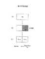
図31及び図32はいずれも液晶表示パネルの1画素の構造を示す概略断面図である。図31は電圧無印加時の状態を示し、図32は電圧印加時の状態を示す。
【0003】
液晶表示パネルは、互いに対向する基板10及び20と、これらの間に封入された、正の誘電率異方性を有するネマティック液晶30とを備えている。基板10では、透明絶縁基板11、例えばガラス基板の一面に、面電極12、誘電体13及び垂直配向層14が積層され、透明絶縁基板11の他面に偏光子15が被着されている。基板20では、透明絶縁基板21、例えばガラス基板の一面に、コモン電極23が形成され、その上に絶縁層24を介して画素電極25が形成されている。絶縁層24及び画素電極25の上には、絶縁層26及び垂直配向層27が積層されている。透明絶縁基板21の他面には、偏光子28が被着されている。偏光子15と28の透過軸は互いに離間して直交している。
【0004】
図示矢印方向のバックライト光がこの液晶表示パネルに入射すると、偏光子28を通って直線偏光になる。面電極12、コモン電極23及び画素電極25が同電位のとき、この直線偏光の偏光面は液晶30内で変化しないので、偏光子15を透過できず、暗状態になる。
【0005】
図32に示す如く、面電極12とコモン電極23とを同電位にし、画素電極25を該電位と異なる電位にすると、電界が生ずる。図32中の点線は、電気力線を示している。この電界により、入射光の方向に対し液晶分子が傾くので、複屈折が生じ、この光の一部が偏光子15を透過して、明状態になる。
【0006】
コモン電極23及び画素電極25は遮光性のメタルであり、これらの上方の液晶分子の挙動は表示上問題にならない。
【0007】
面電極12が存在しないと、画素電極25とコモン電極23との中間の液晶分子の傾斜が小さくなって透過率が落ち込む領域が存在する。面電極12はこの部分の横電界を斜め非対称にして透過率落込を防止するのに寄与する。誘電体13は、液晶30中の横電界を強化して、より低い印加電圧で液晶を駆動可能にするためのものである。コモン電極23と画素電極25とは、紙面垂直方向に延び且つ交互に形成されたストライプ電極である。絶縁層24は、コモン電極23と画素電極25とが後述のように上下に重なる部分で短絡するのを防止するためのものである。絶縁層26は焼付率を低減するためのものである。
【0008】
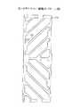
図33は、基板20に形成された電極パターンの1画素分を示す。図34及び図35はそれぞれ、図33中の画素電極25及びコモン電極23のパターン図である。
【0009】
データラインDL1と走査ラインSL1とは、絶縁膜を介して互いに直交している。画素電極25及びコモン電極23はいずれも、ストライプ部と、ストライプ部の端部を繋ぐ周囲部とを有する。ストライプ部は、走査ラインSL1及びデータラインDL1の各々に対し45°傾斜している。
【0010】
走査ラインSL1が高レベルになると、TFT29がオンになって、データラインDL1上の電圧が画素電極25に印加され、画素電極25とコモン電極23のストライプ電極間に電界が生ずる。ストライプ電極の長手方向は、図33の上半分と下半分とで互いに90°異なる。これにより、上半分と下半分とで互いに平行である場合よりも液晶表示パネルの視野角が広くなる。
【0011】
コモン電極23の周囲突起部は、不図示の隣の画素のコモン電極23に繋がっている。
【0012】
図36(A)は、図33中の線電極交差付近の部分拡大図である。図36(B)は、画素電極25とコモン電極23との間に電圧が印加された時の電気力線を点線で示す。
【0013】
画素が矩形であることと、画素電極25及びコモン電極23が互いに平行なストライプ部を有することと、画素電極25及びコモン電極23がいずれも一繋がりのものであることから、画素電極25の周囲部とコモン電極23の周囲部とは絶縁部を介し互いに重なる部分を有する。このため、画素電極25とコモン電極23の隣り合う線電極の端部が、絶縁部を介し交差する。例えば、画素電極25の辺251は、周囲部の辺252に繋がり、コモン電極23の辺231は、辺251と平行であるが辺252とは鋭角で交差している。
【0014】
図37は、液晶表示パネルの1画素の画素電極とコモン電極との間に電圧を印加した場合の電極間付近の液晶分子の傾斜を示す概略断面図である。
【0015】
【発明が解決しようとする課題】
図32において、画素電極25と液晶30との間の構成が、コモン電極23と液晶30との間の構成と異なるので、焼付きが生ずる原因となる。
【0016】
また、図36(B)に示す如く、辺252と辺231とが鋭角で交差するので、この付近の電極間の電界が平行部分のそれよりも強くなる。さらに、交差付近の電界の方向が、平行部分のそれと異なる。このようなことから、交差付近の電極間印加電圧に対する透過特性が平行部分のそれと異なって、画質が劣化するとともに、焼付きが生ずる原因となる。
【0017】
さらに、図37において、画素電極25の上方に絶縁層26が存在するので、これらの部分に電界が印加されても無駄になり、液晶30に対し効率的に電界を印加することができない。垂直配向層27の絶縁性が低いので、この問題を解決するために絶縁層26を省略すると、焼付きが生ずる原因となる。液晶30に対し画素電極25を剥き出しにすると、さらに焼付きが大きくなるとともに、液晶分子が分解する。また、画素電極25の表面が平坦であるので、透過率との関係で液晶30に対し効果的に電界を印加することができず、表示の高コントラスト化が妨げられていた。
【0018】
液晶表示パネルの開発において、焼付率を所定値以下にするために、液晶表示パネルの構造や材料を変える毎に焼付率を測定すると、1回の測定に例えば48時間要するので、開発期間が長くなる。
【0019】
本発明の目的は、このような点に鑑み、焼付率を低減可能な構造の液晶表示パネル及びその開発期間短縮化を可能にする液晶表示パネル開発方法を提供することにある。
【0020】
本発明の他の目的は、表示のコントラストを向上させることが可能な液晶表示パネルを提供することにある。
【0021】
【課題を解決するための手段及びその作用効果】
本発明の液晶表示パネルでは、第1基板と第2基板との間に液晶が封入され、上記第1基板は、絶縁基板と、上記絶縁基板の上方に形成された画素電極及びコモン電極を有する液晶表示パネルにおいて、上記絶縁基板の液晶側の面を基準として、上記画素電極の位置が上記コモン電極の位置よりも高く、上記画素電極と上記コモン電極とが第1絶縁膜を介して重なり合う部分を有し、上記画素電極と上記コモン電極とが上記第1絶縁膜を介して重なり合う部分により、上記画素電極の表面が凸形となっている。上記画素電極が第2絶縁膜で覆われ、上記コモン電極と上記画素電極との間の表示領域に上記第2絶縁膜が実質的に形成されていないことが好ましい。
【0022】
また、上記凸形を形成するために、上記画素電極と上記コモン電極とが上記第1絶縁膜を介して重なり合う部分上に、上記重なり合う部分の上記コモン電極より幅の狭い、TFTの形成のためのチャネル保護膜が形成されていてもよい。上記画素電極が土手形であってもよい。
【0023】
これにより、第1及び第2電極間に同一電圧を印加した場合に、第1電極の表面が平坦である場合よりも液晶分子をより傾斜させることが可能になり、表示のコントラストが向上する。
【0024】
本発明の他の目的、構成及び効果は以下の説明から明らかになる。
【0025】
【発明の実施の形態】
以下、図面を参照して本発明の実施形態を説明する。
【0026】
[第1参考例]
最初に、焼付率を低減可能な構造又は材料を用いた液晶表示パネルの開発期間短縮化を可能にする液晶表示パネル開発方法を説明する。
【0027】
図1は、本発明の方法に用いられる液晶表示装置の概略回路図である。図1では簡単化のために、画素アレイが3行6列の場合を示している。
【0028】
この回路自体は、従来と同一である。データラインDL1、走査ラインSL1、TFT29、画素電極25及びコモン電極23は、例えば図31に示す如く形成されている。画素電極25と対向する電極は、このコモン電極23と、図31に示す面電極12との両方である。走査ライン及びデータラインはそれぞれ、走査ドライバ31及びデータドライバ32の出力端に接続されている。制御回路33は、ピクセルクロックCLK及び水平同期信号HSYNCに基づいてデータドライバ32を制御するとともに、ビデオ信号VSをデータドライバ32に供給し、水平同期信号HSYNC及び垂直同期信号VSYNCに基づいて走査ドライバ31を制御する。走査ドライバ31により、画素アレイの行が順次選択され、選択された行にデータドライバ32から表示データ(階調電圧)が供給される。
【0029】
図2は、焼付率説明図である。
【0030】
例えば、表示データが64階調、「白」が第64階調、「黒」が第1階調である場合を考える。焼付率は次のようにして測定される。
【0031】
(A)白(第64階調)を表示させて輝度Bmを測定する。
【0032】
(B)次に、白と黒の固定パターンを例えば48時間表示させる。
【0033】
(C)この直後に中間調(第32階調)を表示させて、上記(B)で白を表示していた領域と黒を表示していた領域との輝度Bmw及びBmbを測定する。焼付率は、次式で計算される。
【0034】
焼付率=100(Bmw−Bmb)/Bm
上記(C)において、焼付きを人が認識できないようにするためには、焼付率を、室内の通常照明下の場合には6%以下、暗室内の場合には3%以下にしなければならない。
【0035】
焼付率は、液晶表示パネルの構造や構成材料により異なる。液晶表示パネルの開発において、焼付率を所定値以下にするために、液晶表示パネルの構造や材料を変える毎に焼付率を測定すると、1回の測定に例えば48時間要するので、開発期間が長くなる。そこで、焼付率と相関度が高い物理量であって、短時間で測定できるものを探すことを考える。
【0036】
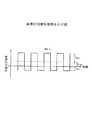
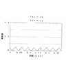
液晶画素には、その劣化を防止するために矩形交流電圧が印加される。図3は、図32の画素電極25とコモン電極23との間及び画素電極25と面電極12との間に印加される電圧波形を示す。周波数は30Hzである。
【0037】
交流電圧印加によりフリッカが生ずるのを防止するため、すなわち透過率が周期的に変化するのを防止するために、液晶画素印加電圧には直流電圧成分が加えられる。矩形交流電圧の振幅及び直流電圧成分をそれぞれVac及びVdcで表す。
【0038】
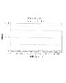
交流振幅Vacを固定し、直流成分Vdcを段階的に変化させた場合の液晶表示パネル透過率を測定した。図4〜図12は、交流振幅Vacを黒表示用電圧である2Vに固定し、直流成分Vdcを−3V、−2V、−1V、−0.5V、0V、0.5V、1V、2V及び3Vにした場合のそれぞれの透過率変動を示す。図4に示す如く、透過率変動幅をΔTで表す。
【0039】
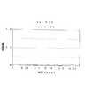
図13は、Vac=2Vの場合の直流成分Vdcと透過率変動幅ΔTとの関係を示すグラフである。このグラフから、透過率変動幅ΔTが最小となる直流成分Vdcの値は−0.38Vと推定される。
【0040】
さらに、交流振幅Vacが白表示用電圧である7Vと中間調表示用電圧(2+7)/2=4.5Vの場合に、透過率変動幅ΔTが最小値ΔTminとなる直流成分Vdcを上記同様にして求めた。これらの結果を、図14に示す。交流振幅Vacが白表示用電圧と黒表示用電圧であるときの直流成分Vdcの差をΔVdcで表す。実際の液晶表示装置では直流成分Vdcが固定値であるので、最適直流成分変動幅ΔVdcが狭いほどフリッカが弱くなる。
【0041】
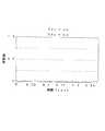
図15は、液晶表示パネルの構造や材料を変えて焼付率及び最適直流成分変動幅ΔVdcを測定し、両者の関係を表したグラフである。このグラフから、焼付率と最適直流成分変動幅ΔVdcとの相関度が高いことが判る。また、焼付率が上記6%以下であるためには、最適直流成分変動幅ΔVdcが0.5V以下でなければならず、焼付率が上記3%以下であるためには、最適直流成分変動幅ΔVdcが0.2V以下でなければならないことが判る。
【0042】
最適直流成分変動幅ΔVdcは短時間で容易に測定することができるので、ΔVdcを用いることにより、焼付率が所望の値以下の液晶表示パネルを開発するための期間を大幅に短縮することが可能となる。
【0043】
なお、図31において、面電極12を用いずに、画素電極25とコモン電極23を用いた構成、及び、コモン電極23を用いずに、画素電極25と面電極12とを用いた構成であっても、最適直流成分変動幅ΔVdcと焼付率との相関度は高く、その他の構成の液晶表示パネルについても同様の相関関係があると考えられる。
【0044】
[第2参考例]
図16及び図17はいずれも、焼付率を低減可能な本発明の第2参考例の液晶画素の構成を示す概略断面図である。図16は電圧無印加時の状態を示し、図17は電圧印加時の状態を示す。
【0045】
この画素を有する液晶パネルは、基板20Aの構成が図22の基板20のそれと異なっている。他の構成は、図22のそれと同一である。
【0046】
図18は、基板20Aの製造工程図である。図18中、右端部はコモン電極23Aと画素電極25Aとが絶縁層24Aを介し重なっている部分に関する。
【0047】
(A)フォトリソグラフィー技術により、透明絶縁基板21上にメタルのコモン電極23Aが形成される。
【0048】
(B)透明絶縁基板21上に絶縁層24が被着される。
【0049】
(C)フォトリソグラフィー技術により、絶縁層24上に画素電極25Aが形成される。
【0050】
(D)画素電極25Aをマスクとして絶縁層24がエッチングされ、画素電極25Aの真下の部分のみ絶縁層24Aが残される。
【0051】
(E)透明絶縁基板21上に絶縁層26Aが被着される。
【0052】
(F)絶縁層26A上に垂直配向層27が積層される。
【0053】
このようにして基板20Aを形成することにより、画素電極25A上の絶縁層26Aの厚みとコモン電極23A上の絶縁層26Aの厚みとが実質的に同一になるので、図17に示す如く画素電極25Aとコモン電極23Aとの間に矩形交流電圧を印加した場合に、コモン電極23Aの上方と画素電極25Aの上方とで電気的状態がほぼ同一になって、図31の構成の液晶表示パネルよりも焼付きが低減される。換言すれば、図15の最適直流成分変動幅ΔVdcがより小さくなって、焼付率が低くなる。
【0054】
絶縁層24A及び26Aは例えば、SiNx、SiO2、レジスト又はアクリル樹脂のいずれかである。試作においては、絶縁層24A及び26AとしてSiNxを用い、垂直配向層27としてJALS204(JSR社)を用い、液晶30としてZLI4535(メルク・ジャパン社)を用い、試作品の焼付率低減効果が確認された。
【0055】
[第3参考例]
図19は、焼付率を低減可能な、本発明の第3参考例の液晶画素の電極パターン図であり、図33と類似している。
【0056】
この電極パターンは、例えば図16の基板20A又は図31の基板20に形成されている。
【0057】
図20及び図21はそれぞれ、図19中の画素電極25A及びコモン電極23Aのパターン図であり、それぞれ図34及び図35と類似している。
【0058】
画素が矩形であることと、画素電極25A及びコモン電極23Aが互いに平行なストライプ部を有することと、画素電極25A及びコモン電極23Aがいずれも一繋がりのものであることから、画素電極25Aの周囲部とコモン電極23Aの周囲部とは、絶縁膜を介し互いに重なる部分を有する。このため、画素電極25Aとコモン電極23Aの隣り合う線電極の端部が、絶縁部を介し交差する。例えば、画素電極25Aの辺251とコモン電極23Aの辺231とは互いに平行であり、辺251及び辺231にそれぞれ連続する辺252と辺232とが交差する。
【0059】
図22(A)は、この電極交差付近の拡大図である。図22(B)は、画素電極25Aとコモン電極23Aとの間に電圧が印加された時の電気力線を点線で示す。
【0060】
辺252と辺232とが鈍角で互いに交差しているので、図36(A)に示すように辺252と辺231とが鋭角で交差する場合よりも、電気力線の集中が緩和されて電界強度が大きくなるのが抑制される。
【0061】
また、辺251と辺231との間を通る線SAに関し辺251及び252と辺231及び232とが対称になっている。これにより、辺252と辺232の間の電界ベクトルの方向は、辺251と辺231との間のそれと平行になる。
【0062】
このようなことから、電極交差付近の透過特性の急変分布が緩和されて、表示画質が向上するとともに、焼付きが低減される。他の電極交差付近についても上記同様である。
【0063】
電極パターン以外は上記試作例と同一にして、図19の電極パターンを用いた液晶パネルと図33の電極パターンを用いた液晶パネルとを試作し、図19の電極パターンを用いた液晶パネルの方が焼付率が低くなることを確認した。
【0064】
[第4参考例]
図23は、焼付率を低減可能な、本発明の第4参考例の液晶画素の電極パターン図であり、図19と類似している。図24は、図23中のコモン電極23Bのパターン図である。画素電極25Aは、図20のそれと同一である。
【0065】
コモン電極23Bの周囲部には、コモン電極23Bの一体性を確保しつつ切除部23B1〜23B8が形成されている。これら切除部23B1〜23B8の位置は、コモン電極23Bと画素電極25Dの、絶縁体を介した交差部付近である。
【0066】
この切除部が無い場合には、電圧印加時にこの部分と画素電極25Aとの間の非表示領域で電界が生じてその付近の表示領域の液晶分子の配列に影響を与える。切除部によりこの影響がなくなるので、上記第3実施形態の場合よりも表示画質が向上すると共に、焼付きが低減される。
【0067】
[第5参考例]
図25は、焼付率を低減可能な、本発明の第5参考例の液晶画素の電極パターン図であり、図33と類似している。図26は、図25中のコモン電極23Cのパターン図である。画素電極25は、図34のそれと同一である。
【0068】
コモン電極23Cは、図24の場合と同様に、コモン電極23Cの一体性を確保しつつ切除部23B1〜23B8が形成されている。これにより、図23の構成と比べて、上記第5実施形態と同じ理由で表示画質が向上すると共に、焼付きが低減される。
【0069】
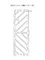
[実施形態]
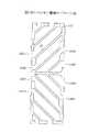
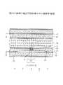
図27は、本発明の実施形態の、隣り合う2つの液晶画素の電極パターン図である。両画素は、同一パターンを有する。
【0070】
コモン電極23Dと画素電極25Dの枠部は、絶縁膜を介し互いに重なっている。画素電極25Dのストライプ電極の下方及び線電極間の下方に、コモン電極23Dのストライプ電極部が形成されており、その線密度は画素電極25Dのそれの2倍である。
【0071】
図28は、図27中のA−A線に沿った断面拡大図である。
【0072】
図32の液晶画素と異なる点は、画素電極25Dの線電極部が凸形であることと、絶縁層26Dが画素電極25D上のみに形成され、コモン電極23Dと画素電極25Dの線電極間表示領域に絶縁層が形成されていないことである。垂直配向層27は絶縁層26Dよりも薄いので、図28ではこれを太線で示している。
【0073】
画素電極25Dの線電極部が凸形であることから、その面が中央線から両側へ傾斜している。該凸形に形成するために、図32と異なり、画素電極25Dの線電極部下方にも、画素電極25Dの線電極部より細幅の、コモン電極23Dの線部が形成されている。この凸形を強調するために、図27のTFT29を作る時に形成されるチャンネル保護膜31が、コモン電極23Dの線部上方に残されている。チャンネル保護膜31の幅は、コモン電極23Dの線部のそれよりも細い。
【0074】
これにより、画素電極25Dの線電極部が土手形となるので、画素電極25Dとコモン電極23Dとの間に電圧を印加した場合に、電気力線が図28中の点線で示すようになる。すなわち、画素電極25Dの傾斜面付近の電気力線がこの面に垂直になるので、液晶分子の傾斜が、透明絶縁基板21の面の法線に対しより大きくなり、図32の場合よりも白表示の透過率が増す。したがって、表示のコントラストが向上する。
【0075】
また、画素電極25Dと絶縁層26Dのパターンが同一で画素電極25Dとコモン電極23Dの間の表示領域に絶縁層26Dが存在しないので、図32の場合よりも液晶分子に対し電界が有効利用され、同じ印加電圧の場合に図32の場合よりもコントラストが向上する。
【0076】
さらに、液晶が画素電極25Dに直接接触しないので、液晶の分解が防止されると共に、焼付きが低減される。
【0077】
図29及び図30は、基板20Dの製造工程を示す。各図は、図27中のB−B線に沿った断面に対応している。次に、これについて説明する。
【0078】
(A)フォトリソグラフィ技術により、透明絶縁基板21上にメタルのコモン電極23D及び走査(ゲート)ラインSL1が形成される。
【0079】
(B)透明絶縁基板21上に絶縁層24、真性半導体膜32及びチャンネル保護膜31が積層される。フォトリソグラフィ技術により、走査ラインSL1とコモン電極23Dの上方のみにチャンネル保護膜31が残される。
【0080】
(D)半導体膜32上にn+半導体膜33、導電膜25D及び絶縁層26Dが積層され、これらが同一パターンで食刻されて、走査ラインSL1の上方にTFT29のソースSとドレインDとが形成されると同時に、コモン電極23Dの線部上方に、画素電極25Dの線電極部及び絶縁層26Dが形成される。画素電極25D並びにTFT29の電極は、3層の導電膜25a、25b及び25cで形成されている。導電膜25a〜25cは例えば、Ti/Al/Tiである。電極25DとしてAl膜のみ用いるとこれがn+半導体膜33内に拡散するので、これを避けるためにTi膜が用いられ、Ti膜のみ用いると抵抗率が高くなるので、Al膜も用いられている。絶縁層26Dは、DVDで形成される窒化シリコン膜又は酸化シリコン膜である。
【0081】
なお、画素電極25Dとして2層のTi/Alを用い、絶縁層26Dとして窒化アルミニウムを用いれば、スパッタ装置でこれらを連続的に成膜することができるので、工程数が削減される。また、絶縁層26Dとしては、パターニングで用いられるフォトレジストを残存させたものであってもよい。
【0082】
(E)絶縁層24上及び26上に、太線で示す垂直配向層27が被着される。
【0083】
本実施形態によれば、画素電極25Dの土手形線電極部及びその上の絶縁層26DがTFT29と同時に形成されるので、画素電極25D及び絶縁層26Dを形成するために工程数を増加する必要がない。
【図面の簡単な説明】
【図1】 本発明の方法に用いられる液晶表示装置の概略回路図である。
【図2】 焼付率説明図である。
【図3】 画素印加電圧波形を示す図である。
【図4】 交流振幅Vacが2V、直流成分Vdcが−3Vである場合の液晶画素透過率測定波形図である。
【図5】 交流振幅Vacが2V、直流成分Vdcが−2Vである場合の液晶画素透過率測定波形図である。
【図6】 交流振幅Vacが2V、直流成分Vdcが−1Vである場合の液晶画素透過率測定波形図である。
【図7】 交流振幅Vacが2V、直流成分Vdcが−0.5Vである場合の液晶画素透過率測定波形図である。
【図8】 交流振幅Vacが2V、直流成分Vdcが0Vである場合の液晶画素透過率測定波形図である。
【図9】 交流振幅Vacが2V、直流成分Vdcが0.5Vである場合の液晶画素透過率測定波形図である。
【図10】 交流振幅Vacが2V、直流成分Vdcが1Vである場合の液晶画素透過率測定波形図である。
【図11】 交流振幅Vacが2V、直流成分Vdcが2Vである場合の液晶画素透過率測定波形図である。
【図12】 交流振幅Vacが2V、直流成分Vdcが3Vである場合の液晶画素透過率測定波形図である。
【図13】 交流振幅Vacが2Vである場合の、直流成分Vdcと液晶画素透過率変動幅ΔTとの関係の測定結果を示すグラフである。
【図14】 交流振幅Vacと液晶画素透過率変動幅ΔTが最小となる直流成分Vdcとの関係の測定結果を示すグラフである。
【図15】 焼付率と最適直流成分変動幅ΔVdcとの関係の測定結果を示すグラフである。
【図16】 本発明の第2参考例の、焼付率を低減可能な液晶画素の構成の電圧無印加状態を示す概略断面図である。
【図17】 図16の液晶画素の電圧印加状態を示す概略断面図である。
【図18】 図16中の基板20Aの製造工程図である。
【図19】 本発明の第3参考例の、焼付率を低減可能な液晶画素の電極パターン図である。
【図20】 図19中の画素電極のパターン図である。
【図21】 図19中のコモン電極のパターン図である。
【図22】 (A)は図19中の電極交差付近の拡大図であり、(B)は(A)の電極間に電圧が印加された時の電気力線を点線で示す図である。
【図23】 本発明の第4参考例の、焼付率を低減可能な液晶画素の電極パターン図である。
【図24】 図23中のコモン電極のパターン図である。
【図25】 本発明の第5参考例の、焼付率を低減可能な液晶画素の電極パターン図である。
【図26】 図25中のコモン電極のパターン図である。
【図27】 本発明の実施形態の、隣り合う2つの液晶画素の電極パターン図である。
【図28】 図27中のA−A線に沿った断面拡大図である。
【図29】 バックライト入射側基板の製造工程を示す図である。
【図30】 図29の続きを示す製造工程図である。
【図31】 本発明と対比される、液晶表示パネルの1画素の構造の電圧無印加状態を示す概略断面図である。
【図32】 図31の画素の電圧印加状態を示す概略断面図である。
【図33】 図32中の基板20に形成された電極パターンの1画素分を示す図である。
【図34】 図33中の画素電極のパターン図である。
【図35】 図33中のコモン電極のパターン図である。
【図36】 (A)は図33中の電極交差付近の拡大図であり、(B)は(A)の電極間に電圧が印加された時の電気力線を点線で示す図である。
【図37】 従来の液晶表示パネルの1画素の画素電極とコモン電極との間に電圧を印加した場合の電極間付近の液晶分子の傾斜を示す概略断面図である。
【符号の説明】
10、20、20A 基板
11、21 透明絶縁基板
12 面電極
13 誘電体
14、27 垂直配向層
15、28 偏光子
23、23A〜23D コモン電極
231、232、251、252 辺
23B1〜23B8 切除部
24、24A、26、26A、26D 絶縁層
25、25A、25D 画素電極
25a〜25c 導電膜
29 TFT
30 液晶
31 チャンネル保護膜
32 半導体膜
33 n+半導体膜
DL1 データライン
SL1 走査ライン[0001]
BACKGROUND OF THE INVENTION
The present invention relates to a liquid crystal display panel having a structure capable of reducing a printing rate and a method for developing the same.
[0002]
[Prior art]
31 and 32 are schematic cross-sectional views showing the structure of one pixel of the liquid crystal display panel. FIG. 31 shows a state when no voltage is applied, and FIG. 32 shows a state when a voltage is applied.
[0003]
The liquid crystal display panel includes
[0004]
When backlight light in the direction indicated by the arrow enters the liquid crystal display panel, the light passes through the
[0005]
As shown in FIG. 32, when the
[0006]
The
[0007]
If the
[0008]
FIG. 33 shows one pixel portion of the electrode pattern formed on the
[0009]
The data line DL1 and the scanning line SL1 are orthogonal to each other through an insulating film. Each of the
[0010]
When the scanning line SL1 becomes high level, the
[0011]
The peripheral protrusion of the
[0012]
FIG. 36A is a partially enlarged view of the vicinity of the line electrode intersection in FIG. FIG. 36B shows a line of electric force when a voltage is applied between the
[0013]
Since the pixel is rectangular, the
[0014]
FIG. 37 is a schematic cross-sectional view showing the inclination of the liquid crystal molecules in the vicinity of the electrode when a voltage is applied between the pixel electrode of one pixel of the liquid crystal display panel and the common electrode.
[0015]
[Problems to be solved by the invention]
In FIG. 32, the configuration between the
[0016]
In addition, as shown in FIG. 36B, since the
[0017]
Further, in FIG. 37, since the
[0018]
In the development of a liquid crystal display panel, if the printing ratio is measured every time the structure or material of the liquid crystal display panel is changed in order to keep the printing ratio below a predetermined value, one measurement takes, for example, 48 hours, so the development period is long. Become.
[0019]
An object of the present invention is to provide a liquid crystal display panel having a structure capable of reducing the printing rate and a liquid crystal display panel development method capable of shortening the development period.
[0020]
Another object of the present invention is to provide a liquid crystal display panel capable of improving display contrast.
[0021]
[Means for solving the problems and their effects]
In the liquid crystal display panel of the present invention, the first substrate and the encapsulated liquid crystal between a second substrate,the first substrate includes an insulating substrate, apixel electrode and acommon electrode formedabove the insulating substrate in the liquid crystal display panel, partially based on the liquid crystal side surface ofthe insulating substrate, overlapping positions ofthe pixel electrode is higher than the position ofthe common electrode, andthe pixel electrode andthe common electrode via the first insulating film the a,the portion where the above-mentioned pixel electrode and the common electrode overlap via the first insulating film, the surface ofthe pixel electrode thathas become convex. Thepixel electrode is covered with the second insulating film, it is preferable that the display area between thecommon electrode andthe pixel electrodeand the second insulating film is not substantially formed.
[0022]
In addition, in order to form the convex shape, on the portion where thepixel electrode and thecommon electrode overlap with each other through the first insulating film, the TFT has a narrower width than thecommon electrode in the overlapping portion.The channel protective film may be formed. Thepixel electrode may be a bank shape.
[0023]
Accordingly, when the same voltage is applied between the first and second electrodes, the liquid crystal molecules can be tilted more than when the surface of the first electrode is flat, and the display contrast is improved.
[0024]
Other objects, configurations and effects of the present invention will become apparent from the following description.
[0025]
DETAILED DESCRIPTION OF THE INVENTION
Hereinafter, embodiments of the present invention will be described with reference to the drawings.
[0026]
[First Reference Example ]
First, a liquid crystal display panel development method capable of shortening the development period of a liquid crystal display panel using a structure or material capable of reducing the printing rate will be described.
[0027]
FIG. 1 is a schematic circuit diagram of a liquid crystal display device used in the method of the present invention. For the sake of simplicity, FIG. 1 shows a case where the pixel array has 3 rows and 6 columns.
[0028]
This circuit itself is the same as the conventional one. The data line DL1, the scanning line SL1, the
[0029]
FIG. 2 is an explanatory diagram of the printing ratio.
[0030]
For example, consider the case where the display data is 64 gradations, “white” is the 64th gradation, and “black” is the first gradation. The seizure rate is measured as follows.
[0031]
(A) White (64th gradation) is displayed and the luminance Bm is measured.
[0032]
(B) Next, a fixed pattern of black and white is displayed for 48 hours, for example.
[0033]
(C) Immediately after this, halftone (32nd gradation) is displayed, and the luminances Bmw and Bmb between the area displaying white and the area displaying black in (B) are measured. The seizure rate is calculated by the following equation.
[0034]
Baking rate = 100 (Bmw−Bmb) / Bm
In (C) above, in order to prevent people from recognizing seizure, the seizure rate must be 6% or less when the room is under normal illumination and 3% or less when the room is in a dark room. .
[0035]
The image sticking rate varies depending on the structure and material of the liquid crystal display panel. In the development of a liquid crystal display panel, if the printing ratio is measured every time the structure or material of the liquid crystal display panel is changed in order to keep the printing ratio below a predetermined value, one measurement takes, for example, 48 hours, so the development period is long. Become. Therefore, it is considered to search for a physical quantity that has a high correlation with the printing rate and can be measured in a short time.
[0036]
A rectangular AC voltage is applied to the liquid crystal pixels in order to prevent the deterioration. FIG. 3 shows voltage waveforms applied between the
[0037]
In order to prevent the occurrence of flicker due to the application of the AC voltage, that is, to prevent the transmittance from changing periodically, a DC voltage component is added to the liquid crystal pixel application voltage. The amplitude and DC voltage component of the rectangular AC voltage are represented by Vac and Vdc, respectively.
[0038]
The transmittance of the liquid crystal display panel was measured when the AC amplitude Vac was fixed and the DC component Vdc was changed stepwise. 4 to 12, the AC amplitude Vac is fixed to 2V which is a black display voltage, and the DC component Vdc is set to -3V, -2V, -1V, -0.5V, 0V, 0.5V, 1V, 2V and Each transmittance variation when 3V is set is shown. As shown in FIG. 4, the transmittance fluctuation range is represented by ΔT.
[0039]
FIG. 13 is a graph showing the relationship between the DC component Vdc and the transmittance fluctuation width ΔT when Vac = 2V. From this graph, it is estimated that the value of the DC component Vdc at which the transmittance fluctuation range ΔT is minimum is −0.38V.
[0040]
Further, when the AC amplitude Vac is 7 V, which is the white display voltage, and the halftone display voltage (2 + 7) /2=4.5 V, the DC component Vdc where the transmittance variation width ΔT becomes the minimum value ΔTmin is set in the same manner as described above. Asked. These results are shown in FIG. The difference between the DC components Vdc when the AC amplitude Vac is the white display voltage and the black display voltage is represented by ΔVdc. In an actual liquid crystal display device, the direct current component Vdc has a fixed value, so that the flicker becomes weaker as the optimum direct current component fluctuation width ΔVdc is narrower.
[0041]
FIG. 15 is a graph showing the relationship between the printing ratio and the optimum DC component fluctuation width ΔVdc measured by changing the structure and materials of the liquid crystal display panel. From this graph, it can be seen that the degree of correlation between the seizure rate and the optimum DC component fluctuation range ΔVdc is high. Further, in order for the seizure rate to be 6% or less, the optimum DC component fluctuation range ΔVdc must be 0.5 V or less, and in order for the seizure rate to be 3% or less, the optimum DC component variation range. It can be seen that ΔVdc must be 0.2V or less.
[0042]
Since the optimum DC component fluctuation range ΔVdc can be easily measured in a short time, using ΔVdc can significantly shorten the period for developing a liquid crystal display panel with a printing rate less than the desired value. It becomes.
[0043]
In FIG. 31, the configuration using the
[0044]
[Second Reference Example ]
16 and 17 are both schematic cross-sectional views showing the configuration of the liquid crystal pixel ofthe second reference example ofthe present invention that can reduce the printing rate. FIG. 16 shows a state when no voltage is applied, and FIG. 17 shows a state when a voltage is applied.
[0045]
In the liquid crystal panel having this pixel, the configuration of the
[0046]
FIG. 18 is a manufacturing process diagram of the
[0047]
(A) A metal
[0048]
(B) An insulating
[0049]
(C) A
[0050]
(D) The insulating
[0051]
(E) An insulating
[0052]
(F) The
[0053]
By forming the
[0054]
Insulating
[0055]
[Third reference example ]
FIG. 19 is an electrode pattern diagram of the liquid crystal pixel ofthe third reference example ofthe present invention capable of reducing the printing rate, and is similar to FIG.
[0056]
This electrode pattern is formed on, for example, the
[0057]
20 and 21 are pattern diagrams of the
[0058]
Since the pixel is rectangular, the
[0059]
FIG. 22A is an enlarged view of the vicinity of this electrode intersection. FIG. 22B shows dotted lines of electric lines when a voltage is applied between the
[0060]
Since the
[0061]
Further, the
[0062]
For this reason, the sudden change distribution of the transmission characteristics in the vicinity of the electrode intersection is relaxed, the display image quality is improved, and the burn-in is reduced. The same applies to the vicinity of other electrode intersections.
[0063]
A liquid crystal panel using the electrode pattern of FIG. 19 and a liquid crystal panel using the electrode pattern of FIG. 33 were made in the same manner as the above prototype except for the electrode pattern, and the liquid crystal panel using the electrode pattern of FIG. Confirmed that the seizure rate was low.
[0064]
[Fourth Reference Example ]
FIG. 23 is an electrode pattern diagram of the liquid crystal pixel ofthe fourth reference example ofthe present invention capable of reducing the printing rate, and is similar to FIG. FIG. 24 is a pattern diagram of the
[0065]
Cutout portions 23B1 to 23B8 are formed around the
[0066]
If there is no cut-out portion, an electric field is generated in the non-display region between this portion and the
[0067]
[Fifth Reference Example ]
FIG. 25 is an electrode pattern diagram of the liquid crystal pixel ofthe fifth reference example ofthe present invention, which can reduce the printing rate, and is similar to FIG. FIG. 26 is a pattern diagram of the
[0068]
As in the case of FIG. 24, the
[0069]
[Embodiment ]
FIG. 27 is an electrode pattern diagram of two adjacent liquid crystal pixels according to theembodiment of the present invention. Both pixels have the same pattern.
[0070]
The frame portions of the
[0071]
FIG. 28 is an enlarged sectional view taken along line AA in FIG.
[0072]
32 is different from the liquid crystal pixel of FIG. 32 in that the line electrode portion of the
[0073]
Since the line electrode portion of the
[0074]
As a result, the line electrode portion of the
[0075]
In addition, since the
[0076]
Further, since the liquid crystal is not in direct contact with the
[0077]
29 and 30 show the manufacturing process of the substrate 20D. Each figure corresponds to a cross section taken along line BB in FIG. Next, this will be described.
[0078]
(A) A metal
[0079]
(B) The insulating
[0080]
(D) An n +
[0081]
Note that if two layers of Ti / Al are used for the
[0082]
(E) A
[0083]
According to the presentembodiment , since the bank line electrode portion of the
[Brief description of the drawings]
FIG. 1 is a schematic circuit diagram of a liquid crystal display device used in a method of the present invention.
FIG. 2 is an explanatory diagram of a printing rate.
FIG. 3 is a diagram showing a pixel applied voltage waveform;
FIG. 4 is a waveform diagram of liquid crystal pixel transmittance measurement when the AC amplitude Vac is 2V and the DC component Vdc is −3V.
FIG. 5 is a waveform chart of liquid crystal pixel transmittance measurement when the AC amplitude Vac is 2V and the DC component Vdc is −2V.
FIG. 6 is a liquid crystal pixel transmittance measurement waveform diagram when the AC amplitude Vac is 2V and the DC component Vdc is −1V.
FIG. 7 is a liquid crystal pixel transmittance measurement waveform diagram when the AC amplitude Vac is 2V and the DC component Vdc is −0.5V.
FIG. 8 is a liquid crystal pixel transmittance measurement waveform diagram when the AC amplitude Vac is 2V and the DC component Vdc is 0V.
FIG. 9 is a liquid crystal pixel transmittance measurement waveform diagram when the AC amplitude Vac is 2V and the DC component Vdc is 0.5V.
FIG. 10 is a liquid crystal pixel transmittance measurement waveform diagram when the AC amplitude Vac is 2V and the DC component Vdc is 1V.
FIG. 11 is a waveform diagram of liquid crystal pixel transmittance measurement when the AC amplitude Vac is 2V and the DC component Vdc is 2V.
FIG. 12 is a waveform chart of liquid crystal pixel transmittance measurement when the AC amplitude Vac is 2V and the DC component Vdc is 3V.
FIG. 13 is a graph showing a measurement result of a relationship between a DC component Vdc and a liquid crystal pixel transmittance variation width ΔT when the AC amplitude Vac is 2V.
FIG. 14 is a graph showing a measurement result of a relationship between an AC amplitude Vac and a DC component Vdc at which the liquid crystal pixel transmittance variation width ΔT is minimized.
FIG. 15 is a graph showing the measurement result of the relationship between the seizure rate and the optimum DC component fluctuation range ΔVdc.
FIG. 16 is a schematic cross-sectional view showing a state in which no voltage is applied in the configuration of a liquid crystal pixel capable of reducing a printing rate, according to asecond reference example ofthe present invention.
17 is a schematic cross-sectional view showing a voltage application state of the liquid crystal pixel of FIG.
FIG. 18 is a manufacturing process diagram for the
FIG. 19 is an electrode pattern diagram of a liquid crystal pixel capable of reducing a printing rate according to athird reference example ofthe present invention.
20 is a pattern diagram of the pixel electrode in FIG. 19. FIG.
FIG. 21 is a pattern diagram of the common electrode in FIG.
22A is an enlarged view of the vicinity of the electrode crossing in FIG. 19, and FIG. 22B is a diagram showing the lines of electric force when a voltage is applied between the electrodes of FIG.
FIG. 23 is an electrode pattern diagram of a liquid crystal pixel capable of reducing a printing rate according to afourth reference example ofthe present invention.
24 is a pattern diagram of the common electrode in FIG. 23. FIG.
FIG. 25 is an electrode pattern diagram of a liquid crystal pixel according to afifth reference example ofthe present invention capable of reducing the printing rate.
26 is a pattern diagram of the common electrode in FIG. 25. FIG.
FIG. 27 is an electrode pattern diagram of two adjacent liquid crystal pixels according to the embodiment of the present invention.
FIG. 28 is an enlarged cross-sectional view taken along line AA in FIG.
FIG. 29 is a diagram showing manufacturing steps of a backlight incident side substrate.
FIG. 30 is a manufacturing process diagram following FIG. 29;
FIG. 31 is a schematic cross-sectional view showing a voltage non-applied state of the structure of one pixel of a liquid crystal display panel, compared with the present invention.
32 is a schematic cross-sectional view showing a voltage application state of the pixel of FIG. 31. FIG.
33 is a diagram showing one pixel of the electrode pattern formed on the
34 is a pattern diagram of the pixel electrode in FIG. 33. FIG.
35 is a pattern diagram of the common electrode in FIG. 33. FIG.
36A is an enlarged view of the vicinity of an electrode crossing in FIG. 33, and FIG. 36B is a diagram showing a line of electric force when a voltage is applied between the electrodes of FIG.
FIG. 37 is a schematic cross-sectional view showing an inclination of liquid crystal molecules in the vicinity of an electrode when a voltage is applied between a pixel electrode and a common electrode of one pixel of a conventional liquid crystal display panel.
[Explanation of symbols]
10, 20,
30
Claims (4)
Translated fromJapanese上記絶縁基板の液晶側の面を基準として、上記画素電極の位置が上記コモン電極の位置よりも高く、上記画素電極と上記コモン電極とが第1絶縁膜を介して重なり合う部分を有し、
上記画素電極と上記コモン電極とが上記第1絶縁膜を介して重なり合う部分により、上記画素電極の表面が凸形となっている、ことを特徴とする液晶表示パネル。Liquid crystal is sealed between the first substrate and the second substrate,the first substrate includes an insulating substrate, in the liquid crystal display panel having apixel electrode and acommon electrode formedabove the insulating substrate,
The position of thepixel electrode is higher than the position of thecommon electrode with respect to the liquid crystal side surface of the insulating substrate, and thepixel electrode and thecommon electrode have a portion overlapping via the first insulating film,
A liquid crystal displaypanel and the pixel electrode and the common electrode by a portion overlapping through the first insulating film, the surface ofthe pixel electrodehas a convex, characterized in that.
Priority Applications (7)
| Application Number | Priority Date | Filing Date | Title |
|---|---|---|---|
| JP2000331570AJP4368515B2 (en) | 2000-10-31 | 2000-10-31 | LCD panel |
| US09/927,005US6819384B2 (en) | 2000-10-31 | 2001-08-09 | Liquid crystal display panel capable of reducing persistence degree and development method thereof |
| TW090121487ATW583480B (en) | 2000-10-31 | 2001-08-30 | Liquid crystal display panel capable of reducing persistence degree and development method thereof |
| KR1020010053819AKR100739846B1 (en) | 2000-10-31 | 2001-09-03 | Liquid crystal display panel |
| US10/747,517US7095473B2 (en) | 2000-10-31 | 2003-12-29 | Liquid crystal display panel capable of reducing persistence degree and development method thereof |
| US11/312,912US7136131B2 (en) | 2000-10-31 | 2005-12-20 | Liquid crystal display panel capable of reducing persistence degree and development method thereof |
| US11/521,778US7397454B2 (en) | 2000-10-31 | 2006-09-15 | Liquid crystal display panel development method |
Applications Claiming Priority (1)
| Application Number | Priority Date | Filing Date | Title |
|---|---|---|---|
| JP2000331570AJP4368515B2 (en) | 2000-10-31 | 2000-10-31 | LCD panel |
Related Child Applications (1)
| Application Number | Title | Priority Date | Filing Date |
|---|---|---|---|
| JP2009092113ADivisionJP5037554B2 (en) | 2009-04-06 | 2009-04-06 | LCD panel |
Publications (2)
| Publication Number | Publication Date |
|---|---|
| JP2002139735A JP2002139735A (en) | 2002-05-17 |
| JP4368515B2true JP4368515B2 (en) | 2009-11-18 |
Family
ID=18807897
Family Applications (1)
| Application Number | Title | Priority Date | Filing Date |
|---|---|---|---|
| JP2000331570AExpired - Fee RelatedJP4368515B2 (en) | 2000-10-31 | 2000-10-31 | LCD panel |
Country Status (4)
| Country | Link |
|---|---|
| US (4) | US6819384B2 (en) |
| JP (1) | JP4368515B2 (en) |
| KR (1) | KR100739846B1 (en) |
| TW (1) | TW583480B (en) |
Families Citing this family (31)
| Publication number | Priority date | Publication date | Assignee | Title |
|---|---|---|---|---|
| JP3966614B2 (en)* | 1997-05-29 | 2007-08-29 | 三星電子株式会社 | Wide viewing angle LCD |
| KR100354904B1 (en) | 1998-05-19 | 2002-12-26 | 삼성전자 주식회사 | Wide viewing angle liquid crystal display device |
| JP4071652B2 (en) | 2002-03-04 | 2008-04-02 | 株式会社 日立ディスプレイズ | Organic EL light emitting display |
| JP4248835B2 (en)* | 2002-04-15 | 2009-04-02 | シャープ株式会社 | Substrate for liquid crystal display device and liquid crystal display device including the same |
| JP4248306B2 (en) | 2002-06-17 | 2009-04-02 | シャープ株式会社 | Liquid crystal display |
| KR100840326B1 (en)* | 2002-06-28 | 2008-06-20 | 삼성전자주식회사 | Liquid crystal display device and thin film transistor substrate used therein |
| JP2004053994A (en)* | 2002-07-22 | 2004-02-19 | Ricoh Co Ltd | Light deflection element and image display device |
| CN100363826C (en)* | 2002-08-26 | 2008-01-23 | 中佛罗里达州大学研究基金会股份有限公司 | High Speed, Wide Viewing Angle LCD Display |
| US7995181B2 (en)* | 2002-08-26 | 2011-08-09 | University Of Central Florida Research Foundation, Inc. | High speed and wide viewing angle liquid crystal displays |
| KR100920344B1 (en) | 2002-12-03 | 2009-10-07 | 삼성전자주식회사 | Thin film transistor array panel for liquid crystal display |
| US7488430B2 (en)* | 2003-03-24 | 2009-02-10 | Lg Display Co., Ltd. | Method of fabricating in-plane switching mode LCD |
| JP4627148B2 (en)* | 2004-04-09 | 2011-02-09 | 株式会社 日立ディスプレイズ | Display device |
| TWI307419B (en)* | 2004-12-27 | 2009-03-11 | Au Optronics Corp | Method of preparing reflective substrate and liquid crystal display device comprising the reflective substrate preparing by the same |
| KR101156510B1 (en)* | 2004-12-30 | 2012-06-18 | 엘지디스플레이 주식회사 | In-plain switching liquid crystal display device |
| KR101122002B1 (en)* | 2004-12-31 | 2012-02-29 | 엘지디스플레이 주식회사 | Liquid Crystal Display Panel and Method of Driving The Same |
| US7697093B2 (en)* | 2006-08-08 | 2010-04-13 | Au Optronics Corp. | Array panel |
| KR101500969B1 (en)* | 2007-04-17 | 2015-03-10 | 코닌클리케 필립스 엔.브이. | Beam shaping device |
| JP2011149967A (en)* | 2008-05-12 | 2011-08-04 | Sharp Corp | Liquid crystal display device |
| RU2469366C2 (en)* | 2008-06-27 | 2012-12-10 | Шарп Кабусики Кайся | Liquid crystal display device |
| CN102187270A (en)* | 2008-10-14 | 2011-09-14 | 夏普株式会社 | Liquid crystal display device |
| TWI405175B (en)* | 2009-02-27 | 2013-08-11 | Au Optronics Corp | Driving method of a liquid crystal sub-pixel |
| TWI403810B (en)* | 2009-11-06 | 2013-08-01 | Innolux Corp | Vertical alignment liquid crystal device |
| WO2012017863A1 (en)* | 2010-08-02 | 2012-02-09 | シャープ株式会社 | Liquid crystal display device |
| KR101798489B1 (en) | 2011-01-14 | 2017-11-17 | 삼성디스플레이 주식회사 | Device for generating gamma, LCD and Method for driving the LCD |
| WO2013018965A1 (en)* | 2011-08-02 | 2013-02-07 | 부산대학교 산학협력단 | Horizontal switching mode liquid crystal display |
| JP5564473B2 (en) | 2011-08-05 | 2014-07-30 | 株式会社ジャパンディスプレイ | Liquid crystal display |
| JP2014112195A (en)* | 2012-10-31 | 2014-06-19 | Japan Display Inc | Liquid crystal display device |
| KR102184447B1 (en)* | 2014-04-10 | 2020-12-01 | 삼성디스플레이 주식회사 | Liquid crystal display and method of measuring of capacitance of liquid crystal display |
| WO2017104623A1 (en)* | 2015-12-16 | 2017-06-22 | コニカミノルタ株式会社 | Display device having irregular shape |
| CN105807860A (en)* | 2016-03-21 | 2016-07-27 | 联想(北京)有限公司 | Safety leather sheath and safety protection method for electronic equipment |
| CN109509458B (en)* | 2019-01-15 | 2021-08-03 | 深圳禾苗通信科技有限公司 | Driving method for eliminating LCD display screen ghost, LCD display screen and storage medium |
Family Cites Families (14)
| Publication number | Priority date | Publication date | Assignee | Title |
|---|---|---|---|---|
| WO1996000408A1 (en) | 1994-06-24 | 1996-01-04 | Hitachi, Ltd. | Active matrix type liquid crystal display device and its driving method |
| JPH08220518A (en)* | 1995-02-15 | 1996-08-30 | Hitachi Ltd | Liquid crystal display device and manufacturing method thereof |
| KR100235592B1 (en)* | 1997-01-22 | 1999-12-15 | 구본준 | Parallel field type liquid crystal display device |
| JP3016223B2 (en)* | 1997-03-11 | 2000-03-06 | 多摩岡産業株式会社 | Nose pad for glasses and method of manufacturing the same |
| JP3780082B2 (en) | 1997-12-05 | 2006-05-31 | 株式会社日立製作所 | Active matrix liquid crystal display device |
| KR100646776B1 (en)* | 1997-10-27 | 2007-06-07 | 삼성전자주식회사 | Manufacturing method of liquid crystal display device |
| TW451099B (en)* | 1998-01-23 | 2001-08-21 | Hitachi Ltd | Liquid crystal display device |
| KR100304915B1 (en)* | 1998-04-09 | 2001-09-24 | 구본준, 론 위라하디락사 | Liquid crystal display device of composite switching mode |
| KR100293809B1 (en)* | 1998-05-29 | 2001-10-26 | 박종섭 | IP-V Mode LCD Display with Multiple Domains |
| KR100487424B1 (en)* | 1998-07-09 | 2005-08-29 | 엘지.필립스 엘시디 주식회사 | Hybrid switching mode liquid crystal display device and method of making the same |
| TWI251697B (en)* | 1999-05-26 | 2006-03-21 | Matsushita Electric Industrial Co Ltd | Liquid crystal display element and producing method thereof |
| KR100433596B1 (en)* | 1999-10-21 | 2004-05-31 | 마쯔시다덴기산교 가부시키가이샤 | Liquid crystal device |
| KR100380222B1 (en)* | 2000-10-13 | 2003-04-16 | 엘지.필립스 엘시디 주식회사 | array substrate for in-plane switching mode liquid crystal display device |
| JP2004109794A (en)* | 2002-09-20 | 2004-04-08 | Hitachi Displays Ltd | Liquid crystal display |
- 2000
- 2000-10-31JPJP2000331570Apatent/JP4368515B2/ennot_activeExpired - Fee Related
- 2001
- 2001-08-09USUS09/927,005patent/US6819384B2/ennot_activeExpired - Lifetime
- 2001-08-30TWTW090121487Apatent/TW583480B/ennot_activeIP Right Cessation
- 2001-09-03KRKR1020010053819Apatent/KR100739846B1/ennot_activeExpired - Fee Related
- 2003
- 2003-12-29USUS10/747,517patent/US7095473B2/ennot_activeExpired - Lifetime
- 2005
- 2005-12-20USUS11/312,912patent/US7136131B2/ennot_activeExpired - Lifetime
- 2006
- 2006-09-15USUS11/521,778patent/US7397454B2/ennot_activeExpired - Lifetime
Also Published As
| Publication number | Publication date |
|---|---|
| US20060103801A1 (en) | 2006-05-18 |
| US7397454B2 (en) | 2008-07-08 |
| TW583480B (en) | 2004-04-11 |
| US20040141134A1 (en) | 2004-07-22 |
| US6819384B2 (en) | 2004-11-16 |
| KR100739846B1 (en) | 2007-07-16 |
| US7095473B2 (en) | 2006-08-22 |
| US20020051109A1 (en) | 2002-05-02 |
| JP2002139735A (en) | 2002-05-17 |
| US7136131B2 (en) | 2006-11-14 |
| US20070008476A1 (en) | 2007-01-11 |
| KR20020034857A (en) | 2002-05-09 |
Similar Documents
| Publication | Publication Date | Title |
|---|---|---|
| JP4368515B2 (en) | LCD panel | |
| KR100737882B1 (en) | Substrate for a liquid crystal display device, liquid crystal display device having it, and driving method of a liquid crystal display device | |
| JP5680343B2 (en) | Liquid crystal display device and thin film transistor substrate used therefor | |
| KR100846276B1 (en) | Liquid crystal display device | |
| JP3127894B2 (en) | Active matrix type liquid crystal display | |
| US20060215066A1 (en) | Substrate for liquid crystal display, liquid crystal display having the substrate, and method of driving the display | |
| KR20080007203A (en) | LCD and its driving method | |
| US7136132B2 (en) | Liquid crystal display device and manufacturing method therefor | |
| US8581819B2 (en) | Apparatus and method for driving liquid crystal display device | |
| US8614721B2 (en) | Liquid crystal display device and potential setting method for the same | |
| JP3481074B2 (en) | Liquid crystal display device | |
| JP2005055880A (en) | Liquid crystal display device and driving method thereof | |
| WO2011024966A1 (en) | Liquid crystal display | |
| KR100690513B1 (en) | Liquid crystal display | |
| JP4566579B2 (en) | Driving method of liquid crystal display device | |
| KR100649515B1 (en) | Liquid crystal display apparatus and liquid crystal television and liquid crystal monitor adopting same | |
| JP5037554B2 (en) | LCD panel | |
| JP5222389B2 (en) | LCD panel | |
| JP4870945B2 (en) | Liquid crystal display | |
| JP2012073640A (en) | Liquid crystal display panel | |
| JP2006201594A (en) | Liquid crystal display | |
| CN100419558C (en) | Liquid crystal display panel and active element array substrate thereof | |
| JPH08234208A (en) | Liquid crystal display device | |
| KR101074378B1 (en) | Method for supplying reference voltage and Driving method for Liquid Crystal Display using the same | |
| KR20060102220A (en) | Display |
Legal Events
| Date | Code | Title | Description |
|---|---|---|---|
| A711 | Notification of change in applicant | Free format text:JAPANESE INTERMEDIATE CODE: A711 Effective date:20050712 | |
| A711 | Notification of change in applicant | Free format text:JAPANESE INTERMEDIATE CODE: A711 Effective date:20050713 | |
| RD02 | Notification of acceptance of power of attorney | Free format text:JAPANESE INTERMEDIATE CODE: A7422 Effective date:20050722 | |
| A621 | Written request for application examination | Free format text:JAPANESE INTERMEDIATE CODE: A621 Effective date:20061011 | |
| A977 | Report on retrieval | Free format text:JAPANESE INTERMEDIATE CODE: A971007 Effective date:20080806 | |
| A131 | Notification of reasons for refusal | Free format text:JAPANESE INTERMEDIATE CODE: A131 Effective date:20080819 | |
| A521 | Written amendment | Free format text:JAPANESE INTERMEDIATE CODE: A523 Effective date:20081017 | |
| A131 | Notification of reasons for refusal | Free format text:JAPANESE INTERMEDIATE CODE: A131 Effective date:20090203 | |
| A521 | Written amendment | Free format text:JAPANESE INTERMEDIATE CODE: A523 Effective date:20090406 | |
| TRDD | Decision of grant or rejection written | ||
| A01 | Written decision to grant a patent or to grant a registration (utility model) | Free format text:JAPANESE INTERMEDIATE CODE: A01 Effective date:20090825 | |
| A01 | Written decision to grant a patent or to grant a registration (utility model) | Free format text:JAPANESE INTERMEDIATE CODE: A01 | |
| A61 | First payment of annual fees (during grant procedure) | Free format text:JAPANESE INTERMEDIATE CODE: A61 Effective date:20090826 | |
| R150 | Certificate of patent or registration of utility model | Ref document number:4368515 Country of ref document:JP Free format text:JAPANESE INTERMEDIATE CODE: R150 Free format text:JAPANESE INTERMEDIATE CODE: R150 | |
| FPAY | Renewal fee payment (event date is renewal date of database) | Free format text:PAYMENT UNTIL: 20120904 Year of fee payment:3 | |
| FPAY | Renewal fee payment (event date is renewal date of database) | Free format text:PAYMENT UNTIL: 20130904 Year of fee payment:4 | |
| LAPS | Cancellation because of no payment of annual fees |