JP4366921B2 - Personal verification device, card-type information recording medium, and information processing system using the same - Google Patents
Personal verification device, card-type information recording medium, and information processing system using the sameDownload PDFInfo
- Publication number
- JP4366921B2 JP4366921B2JP2002325133AJP2002325133AJP4366921B2JP 4366921 B2JP4366921 B2JP 4366921B2JP 2002325133 AJP2002325133 AJP 2002325133AJP 2002325133 AJP2002325133 AJP 2002325133AJP 4366921 B2JP4366921 B2JP 4366921B2
- Authority
- JP
- Japan
- Prior art keywords
- pulse wave
- index
- information
- detection sensor
- unit
- Prior art date
- Legal status (The legal status is an assumption and is not a legal conclusion. Google has not performed a legal analysis and makes no representation as to the accuracy of the status listed.)
- Expired - Fee Related
Links
Images


Classifications
- G—PHYSICS
- G06—COMPUTING OR CALCULATING; COUNTING
- G06V—IMAGE OR VIDEO RECOGNITION OR UNDERSTANDING
- G06V40/00—Recognition of biometric, human-related or animal-related patterns in image or video data
- G06V40/10—Human or animal bodies, e.g. vehicle occupants or pedestrians; Body parts, e.g. hands
- G06V40/12—Fingerprints or palmprints
- G06V40/13—Sensors therefor
- G06V40/1306—Sensors therefor non-optical, e.g. ultrasonic or capacitive sensing
Landscapes
- Engineering & Computer Science (AREA)
- Human Computer Interaction (AREA)
- Physics & Mathematics (AREA)
- General Physics & Mathematics (AREA)
- Multimedia (AREA)
- Theoretical Computer Science (AREA)
- Measurement Of The Respiration, Hearing Ability, Form, And Blood Characteristics Of Living Organisms (AREA)
- Image Input (AREA)
- Measuring Pulse, Heart Rate, Blood Pressure Or Blood Flow (AREA)
Description
Translated fromJapanese【0001】
【発明の属する技術分野】
本発明は、本人照合装置、カード型情報記録媒体及びそれを用いた情報処理システムに関する。
【0002】
【背景技術】
本人照合のために、指紋検出センサを用いる技術が提案され、抵抗感知型指紋検出センサ(例えば、特許文献1参照。)と、光電式指紋検出センサ(例えば、特許文献2参照。)と、圧電式指紋検出センサ(例えば、特許文献3参照。)と、静電容量式指紋検出センサ(例えば、特許文献4参照。)とがそれぞれ提案されている。
【0003】
【特許文献1】
特開平3−6791号公報
【特許文献2】
特開平4−271477号公報
【特許文献3】
特開平5−61965号公報
【特許文献4】
特開平11−118415号公報
【0004】
【背景技術及び発明が解決しようとする課題】
しかし、本人照合を指紋だけに頼ると、その本人が生存していない場合にも指紋を採取できるので、犯罪に悪用される懸念がある。
【0005】
特開2001−184490は、読み取りローラ上を走査される指の指紋を工学的に読み取ると共に、その近傍に設けた脈拍センサにより脈拍を検出する技術が開示されている。しかし、脈拍はパルスであるので偽造がた易い。また、指紋検出に読み取りローラを用いているため、例えば携帯用カードにその構造を採用することは不可能である。
【0006】
そこで、本発明の目的は、本人照合精度が高く、しかも照合対象物の偽造が極めて困難な本人照合装置並びにそれを用いたカード型情報記録媒体及び情報処理システムを提供することにある。
【0007】
【課題を解決するための手段】
本発明の一態様に係る本人照合装置は、操作者の固有情報を検出する第1の検出手段と、前記操作者の脈波を検出する第2の検出手段と、前記第2の検出手段にて検出された脈波を処理して、少なくとも一つの指標を抽出する指標抽出手段と、前記固有情報と比較される第1の比較情報を記憶する第1の記憶手段と、前記少なくとも一つの指標と比較される第2の比較情報を記憶する第2の記憶手段と、前記固有情報と前記第1の比較情報との比較結果に基づいて、前記操作者が登録された本人と一致され、かつ、前記少なくとも一つの指標と前記第2の比較情報との比較結果に基づいて、前記操作者が生存していると判断された時に、前記操作者が真正であることを示す信号を出力する照合手段とを有する。真正である事を示す信号は表示情報であっても良いし、或いは暗号化されたパスワードであっても良いし、パスワードが電子信号として出力されても良い。
【0008】
ここで、操作者の固有情報としては、指紋、虹彩、歯形、手相、顔相、声紋などがあるが、第1の検出手段にて検出される固有情報としては指紋が好適である。このような固有情報は、個人識別には好適であるが、その操作者が生体でなくても採取できる。そこで、第2の検出手段では、生存している操作者からのみ発せられる脈波を検出している。検出された脈波は処理され、指標抽出部にて脈波中から指標が抽出される。脈波の形状は生存する人間固有のものであり、脈波から抽出される指標もまた、生存する人間固有のものである。このように指標化することで、既知記憶情報との比較も容易となる。この点、脈波自体でなく、その一成分である例えば脈拍等のパルスを直接検出しようとした場合、そのようなパルスは人為的に生成可能である。一方、脈波の波形を偽造することは極めて困難であり、かつ、その脈波中のいずれかの指標をも偽造することは不可能に近い。よって、本発明の一態様によれば、本人照合精度が極めて向上し、本人照合結果の信頼性が向上する。
【0009】
本発明の一態様では、前記指標抽出手段は、以下の各種形態にて構成できる。この指標抽出部は、前記第2の検出手段にて検出された脈波が極大(増加から減少に変わる)または極小(減少から増加に変わる)となる複数の変化点の少なくとも一つの波高を、前記少なくとも一つの指標として抽出する波高抽出部を含むことができる。あるいは、前記指標抽出手段は、前記第2の検出手段にて検出された脈波が極大または極小となる複数の変化点の少なくとも一つに至るまでの時間を、前記少なくとも一つの指標として抽出する時間抽出部を含むことができる。あるいは、前記指標抽出手段は、前記第2の検出手段にて検出された脈波が極大または極小となる複数の変化点の波高比率を、前記少なくとも一つの指標として抽出する波高比率抽出部を含むことができる。あるいは、前記指標抽出手段は、前記第2の検出手段にて検出された脈波の加速度波形を演算する演算部と、前記加速度波形が極大または極小となる複数の変化点の波高比率を、前記少なくとも一つの指標として抽出する波高比率抽出部を含むことができる。あるいは、前記指標抽出手段は、前記第2の検出手段にて検出された脈波極大または極小となる複数の変化点間の時間比率を、前記少なくとも一つの指標として抽出する時間比率抽出部を含むことができる。この場合、前記時間比率抽出部は、前記第2の検出手段にて検出された脈波より、該脈波の周期と駆出時間との比率を抽出することができる。あるいは、前記指標抽出手段は、前記第2の検出手段にて検出された脈波を増幅する増幅器とすることができる。この増幅器は、オート・ゲイン・コントロール機能により前記脈波を一定振幅以上の信号に増幅した時の増幅倍率を指標として抽出する。この指標としての増幅倍率は、血管年齢と同等の生体の個人情報となり得る。
【0010】
本発明の一態様では、前記指標抽出手段にて抽出された前記少なくとも一つの指標の履歴情報を記憶する履歴情報記憶部と、前記履歴情報に基づいて、前記第2の記憶手段に記憶されている前記第2の比較情報を更新する情報更新部とをさらに含むことができる。履歴情報に基づいて第2の比較情報を更新することで、例えば経時的に変化する指標に合わせて第2の比較情報を変更したり、あるいは比較の許容幅を履歴情報に基づいて狭くしたりすることができる。
【0011】
本発明の一態様にて前記固有情報を指紋とした場合には、前記第1の検出手段は指紋検出センサであり、前記第1の記憶手段には本人の指紋情報が記憶される。
【0012】
この指紋検出センサは、前記操作者の指の凹凸に応じて変化する静電容量を検出することで、指紋を検出することができる。
【0013】
このような指紋検出センサは、M(Mは2以上の整数)行の電源線と、N(Nは2以上の整数)列の出力線と、前記M行N列の電源線及び出力線の各交点にそれぞれ設けられたM×N個の静電容量検出素子とを含むことができる。
【0014】
前記M×N個の静電容量検出素子の各々は、信号検出素子と信号増幅素子とを含み、前記信号検出素子は、容量検出電極と容量検出誘電体膜とを含み、前記信号増幅素子を、ゲート電極、ゲート絶縁膜及び半導体膜を有する信号増幅用MIS型薄膜半導体装置にて形成することができる。
【0015】
ここで、指紋検出センサは、前記M行の電源線に接続される電源選択回路をさらに有することができる。この電源選択回路は、共通電源線と前記M行の電源線との間に設けられたM個の電源用パスゲートとを含み、前記M個の電源用パスゲートの各々を、ゲート電極、ゲート絶縁膜及び半導体膜を有する信号増幅用MIS型薄膜半導体装置にて形成することができる。
【0016】
さらに、指紋検出センサは、前記N行の信号線に接続される信号選択回路をさらに有することができる。この信号選択回路は、共通出力線と前記N列の出力線との間に設けられたN個の出力信号用パスゲートとを含み、前記N個の出力信号用パスゲートの各々を、ゲート電極、ゲート絶縁膜及び半導体膜を有する信号増幅用MIS型薄膜半導体装置にて形成することができる。
【0017】
本発明の一態様では、前記指紋検出センサへの指の接触を検知して、本人照合装置を起動させる起動スイッチをさらに有することができる。
【0018】
本発明の一態様では、前記第2の検出手段は、発光素子と受光素子とを有する脈波検出センサを含み、前記操作者の脈波を光学的に検出することができる。この場合、前記第2の検出手段は、発光素子と受光素子とを有する脈波検出センサを含み、前記指紋検出センサが表面側に位置するようにして、前記指紋検出センサと前記脈波検出センサとが積層され、かつ、前記指紋検出センサが前記発光素子からの発光経路及び前記受光素子への受光経路と交差する領域を、前記発光素子からの発光波長に対して透明な部材により形成することができる。
【0019】
ここで、前記指紋検出センサにて検出された指紋が真正でないと前記照合手段により判断された時は、前記脈波検出センサでの脈波の検出が禁止することができる。それにより電力を比較的多く消費する光学的な脈波検査を省略できる。
【0020】
前記脈波検出センサにて検出された脈波から低域周波数成分を遮断する低域遮断フィルタをさらに有することができる。低域周波数帯域には、交感神経系機能または副交感神経系機能などの自律神経系機能を反映した周波数成分や、体動に起因した周波数成分が含まれているので、これらを除去する必要があるからである。特にこの低域遮断フィルタは、低域遮断周波数を0.4〜0.5Hzの範囲中の値に設定すると良い。上記のような無駄な周波数成分のみを除去でき、しかも脈波波形の特徴が損なわれないからである。
【0021】
本発明の他の態様に係る本人照合装置は、経時的に変化する操作者の生体情報を検出する検出手段と、前記生体情報と比較される比較情報を記憶する第1の記憶手段と、前記検出手段で検出された前記生体情報の履歴情報を記憶する第2の記憶手段と、前記第2の記憶手段に記憶された履歴情報に基づいて、前記第1の記憶手段内の比較情報を更新する更新手段と、前記生体情報と前記比較情報との比較結果に基づいて、前記操作者が真正であることを示す信号を出力する照合手段とを有する。
【0022】
ここで、生体情報とは、脈波、脳波、心電、筋電、体表温、体表からの輻射熱などを挙げることができるが、このうち、経時的に変化する生体情報として脈波を好適に挙げることができる。特に脈波の加速度波形中の変化点の波高比率は年齢依存性を有する。このように経時的に変化する生体情報と比較される比較情報は、時の経過に応じて更新される必要がある。本発明の他の態様では、生体情報を検出する度に履歴情報として記憶しておき、その履歴情報に基づいて比較情報を更新している。このように比較情報が自動更新されるので、自動更新機能を有する本人照合装置は、半永久的に使用可能となる。比較情報としては生体情報の移動平均値と、移動平均値から生体情報の乖離度を示す偏差とを用いる。最新の過去数回の移動平均から、次回移動平均値を推定し、その推定値を中心に偏差のk倍(1≦k≦3)の値を次回生体情報の許容範囲とする。こうする事で、本人を他人と間違えて拒絶することを著しく低減でき、且つ脈波の偽造に依る不正使用を防止できる。
【0023】
本発明のさらに他の態様に係るカード型情報記録媒体は、上述した本人照合装置を内蔵するものである。
【0024】
特に、指紋検出センサの裏に脈波検出センサを備えた本人照合装置を有するカード型情報記録媒体は、少なくとも前記脈波検出センサが形成された第1の薄膜ディバイスと、少なくとも前記指紋検出センサが形成された第2の薄膜ディバイスとが積層して形成することができる。
【0025】
これらのカード型情報記録媒体は、前記照合手段からの前記信号に基づいて、カード使用可能状態であることを表示する表示部をさらに有することができる。
【0026】
本発明のさらに他の態様に係る情報処理システムは、上述のカード型情報記録媒体と、前記カード型情報記録媒体の情報に基づいて処理する情報処理装置とを有し、前記情報処理装置は、前記照合手段から前記信号が入力された後に、前記カード型情報記録媒体から、本人照合に用いた情報以外の情報を読み取るものである。
【0027】
こうすると、本人照合に用いられた個人情報は、カード型情報記録媒体内部でのみ処理され、外部に漏出することがない。
【0028】
ここで、前記情報処理装置は、前記カード型情報記録媒体に給電する給電部を有することができる。もちろん、カード型情報記録媒体内部に電源を内蔵させても良い。
【0029】
【発明の実施の形態】
以下、本発明を、本人照合装置を内蔵したカード型情報記録媒体及びそれを用いた情報処理システムに適用した実施形態について、図面を参照して説明する。
【0030】
(カード型情報記録媒体)
例えば集積回路(IC)を含むICカードとして、メモリカード、I/O(入出力回路)カード、ISO準拠のカードなどが知られている。本実施形態は、これらのクレジットカード、キャッシュカード等として用いられる各種カードに本人照合装置を内蔵させたものである。
【0031】
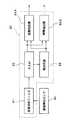
一例として、本実施形態のカード型情報記録媒体の例を、図1(A)〜図1(C)及び図2(A)(B)に示す。図1(A)に示すカードは基板10上にメモリ12を有し、図1(B)に示すカードはメモリ12に加えさらにCPU14を有し、図1(C)に示すカードはメモリ12及びCPU14に加えさらにI/O16を有する。図2(A)に示すカードは図1(C)に示すカードに表示部20及び表示駆動部22をさらに加えたものである。図2(B)に示すカードは図2(A)に示すカードにさらに電源例えば太陽電池24を付加したものである。この他、カードに内蔵される構成は種々変形でき、例えば図2(B)以外のカードにも電源例えば太陽電池24を内蔵させても良い。
【0032】
ここで、図1(A)〜図1(C)及び図2(A)(B)に示すいずれのカードにも本人照合装置30が内蔵されている。
【0033】
(情報処理システム)
図3は、カード型情報記録媒体100と情報処理装置110とから構成される情報処理システムを示している。本実施形態のカード型情報記録媒体100のセンシング領域に、カード所有者が指を触れると、カード型情報記録媒体100がカード所有者の指紋と脈波とを検出し、本人照合装置30にて本人照合が実施される。この照合動作は、カード型情報記録媒体100が電源を内蔵していれば、情報処理装置110から電力の供給を受けずに実施できる。カード型情報記録媒体100が電源を内蔵していなければ、情報処理装置110の給電部112から電力の供給を受けて実施できる。
【0034】
情報処理装置110は、カード型情報記録媒体100にてカード所有者が登録された本人であると認証された後に、カード型情報記録媒体100から、本人照合に用いた情報以外の各種情報を読み取って処理する。カード型情報記録媒体100からの認証結果の出力形態として、カード型情報記録媒体100が表示部20(図2(A)(B)参照)を有するのであれば、その表示部20に「カード使用可能」などの使用許可情報を表示すればよい。情報処理装置110を操作するオペレータは、その表示を確認した後に情報処理を開始できる。カード型情報記録媒体がクレジットカードであり、電源を内蔵していると、この表示情報を確認する事だけで、クレジットカードの不正使用は著しく低減される。又店に情報処理装置が設置されてなくとも、カード使用者の本人認証が可能になる。あるいは、カード型情報記録媒体100にて本人であると認証された後に、カード型情報記録媒体100からパスワード等が電子情報などの形態で出力されて、情報処理装置110に入力されるようにしても良い。こうすると、オペレータを介在させずに情報処理装置110での処理が開始される。情報処理装置110は、カード発行会社のホスト機器120の端末機器として機能し、カード型情報記録媒体100からのパスワードを、ホスト機器120からの情報に基づいて照合する機能を有するものでも良い。
【0035】
いずれの場合も、カード型情報記録媒体100は真正なる本人以外は使用不能のとなるので、カードの紛失、盗難があっても、カードの盗用が防止される。しかも、指紋、脈波などの個人情報は、カード型情報記録媒体100から外部に読み出されることがないので、個人情報の流出も防止できる。
【0036】
(本人照合装置)
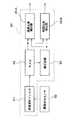
図4は、カード型情報記録媒体100に内蔵される本人照合装置30のブロック図である。図4において、この本人照合装置30には、カード所有者の固有情報を検出する第1の検出手段としての指紋検出センサ40と、カード所有者の脈波を検出する第2の検出手段としての脈波検出センサ50とが設けられている。これらの各センサ40,50の詳細については後述する。指紋検出センサ40にカード所有者の指が接触されたことを感知して、本人照合装置30を起動させる起動スイッチ42を設けることもできる。特に、カード型情報記録媒体100が電源を内蔵している場合に、省エネルギーの観点から起動スイッチ42を設ける意義がある。
【0037】
脈波検出センサ50にて検出された脈波を処理して、少なくとも一つの指標を抽出する指標抽出部60が設けられている。
【0038】
指紋検出センサ40からの指紋情報と、指標抽出部60からの抽出情報とは、照合部70に入力される。この照合部70は、比較情報記憶部80に記憶された比較情報と検出情報とを照合するものである。比較情報記憶部80は、指紋検出センサ40からの指紋情報と比較される第1の比較情報が記憶される第1の比較情報記憶部82と、指標抽出部60からの指標と比較される第2の比較情報が記憶される第2の比較情報記憶部84とを有する。また、照合部70からの照合結果に基づいて、カード所有者が真正であるからカードの使用を許可する信号、例えば暗号化されたパスワードを出力するパスワード出力部90が設けられている。なお、照合部70からの信号は、カード型情報記録媒体100のCPU14にも入力され、例えば図2(A)(B)に示す表示部20にカードの使用を許可する旨の表示、例えば「カード使用可能」などのメッセージの表示、あるいはその旨の点灯または点滅表示などを制御する。
【0039】
本人照合装置30は更に過去の抽出情報を記憶する履歴情報記憶部130と情報更新部140とを備えている。履歴情報記憶部130は過去に照合して本人と認証された抽出情報を記憶しておく部位である。過去に正しいと判定された抽出情報を基に最新の情報に更新するのが情報更新部140で、これにより第2の比較情報の許容範囲が定まり、この許容範囲が第2の比較情報記憶部84に記憶される。
【0040】
(脈波検出センサ及び指標抽出部)
脈波検出センサ50は圧電式でも構成できるが、ここでは光学的に検出する例を説明する。この場合、脈波検出センサ50は発光素子(発光ダイオード、面発光レーザ、有機ELなど)と受光素子(フォトダイオードやフォトトランジスタなど)とを用いて構成することができる。これらの素子はモノシリックで形成されることにより、小型で安価となる。
【0041】
発光素子からの発光波長は、血液中のヘモグロビンの吸収波長ピーク付近に選定されることが好ましい。受光レベルが血流量に応じて変化するので、脈波(例えば容積脈波)波形を検出することができる。このような発光素子としては、InGaN系(インジウム−ガリウム−窒素系)の青色LEDなどを用いることができ、発光波長は350〜600nm(ピーク波長は450nm付近)である。受光素子としては、例えばGaAsP系(ガリウム−砒素−リン系)のフォトトランジスタなどを用いることができ、主要感度領域は300〜600nmである。なお、外光のうち波長が700nm以下の光は指の組織を透過しにくい傾向がある。よって、カードに指を接触させた状態で脈波を検出しても、S/Nを高く確保できる。
【0042】
脈波検出センサ50をカード型情報記録媒体100に内蔵させることを考慮すると、この脈波検出センサ50は、例えば、本願出願人により出願された特開平9−27611号、特開平11−330532号等に開示された構造などを採用することができる。いずれの公報も、発光素子としての面発光型半導体レーザと、受光素子としてのフォトダイオードとを、半導体製造プロセスを用いて、基板上に隣接して形成し、かつ電気的に断絶させて形成したものである。これらの構造を用い、材質を適宜選択して上述の発光波長、受光波長を持つ薄膜の脈波検出センサ50を形成することができる。
【0043】
図5は、脈波検出センサ50にて検出された脈波の1拍分の波形を示している。図5に示すように、この脈波には下記の特徴がある。
(1)1拍分の脈波に順次極大または極大となる複数の変化点P1〜P5が現われる。
(2)変化点P1〜P5は、波高y1〜y5を有する。
(3)脈波開始時刻t0を基準として、各変化点P1〜P5が出現するまでの時間はT1〜T5であり、次の1拍の脈波が開始するまでの経過時間(周期)はT6である。
【0044】
本実施形態では、このような変化点P1〜P5の波高y1〜y5の少なくとも一つか、あるいは時刻t0から変化点P1〜P5のいずれかが生ずるまでの時間T1〜T5または周期T6の少なくとも一つを、指標抽出部60が抽出することができる。
【0045】
このような脈波は、生体から発せられる生体信号であり、それを処理して抽出した指標も生体独自のものである。よって、このような指標を抽出できれば、切断された指をモニタしたものでなく、確かに生存するカード所有者の指をモニタしたものであることが判明する。この点、脈波自体でなく、その一成分である例えば脈拍等のパルス(即ち周期)を直接検出しようとした場合、そのようなパルスは人為的に生成可能である。本実施形態では、人為的に偽造が困難な脈波を検出し、それを処理して抽出される指標を比較しているので、カードの盗用は確実に防止される。
【0046】
上述した指標は、図6に示す指標抽出部60にて抽出できる。低域遮断フィルタ61は、脈波検出センサ50にて検出された脈波のうち、所定のカットオフ周波数よりも低域の周波数を遮断し、高域周波数のみを取り出す。遮断された低周波数帯域には、副交感神経系機能である例えば呼吸性の変動(例えば0.15Hz)や、交感神経系機能である例えば筋ポンプ作用のマイヤーウェーブ(例えば0.1Hz)など、自律神経機能を反映する成分が含まれている。さらにこの低周波数帯域には、体動に伴う周波数成分も含まれている。低域遮断フィルタ61は、心臓の拍動に基づく脈波波形を阻害する不要な低周波数帯域を除去できる。
【0047】
低域遮断フィルタ61は、低域遮断周波数を0.4〜0.5Hzの範囲中の値とすることが好ましい。0.4〜0.5Hzを越える周波数を遮断すると、心臓の拍動に基づく脈波波形の特徴が失われてしまうからである。
【0048】
RAM62はワーキングメモリとして機能し、低域遮断フィルタ61の出力が記憶される。微分回路63は、低域遮断フィルタ61の出力波形を時間微分する。微分値として0が出力された点が変化点P1〜P5となる。波高抽出部64Aは、RAM62内の波形の中から、微分回路63からの微分値0に対応する変化点P1〜P5の波高y1〜y5の少なくとも一つを、指標として抽出する。時間抽出部64Bは、時刻t0から変化点P1〜P5に至るまでの時間T1〜T5の少なくとも一つを、指標として抽出する。なお、波高抽出部64A及び時間抽出部64Bのいずれか一方のみを設けるものでも良い。
【0049】
図6に代えて、図7に示す指標抽出部60を用いても良い。図7では、波高抽出部64Aに代えて波高比率抽出部65Aが、時間抽出部64Bに代えて時間比率抽出部65Bが設けられている。波高比率抽出部65Aは、波高y1〜y5のうちの任意の2つの波高比率、例えばy2/y1,y3/y1,y4/y1,y5/y1などのうち少なくとも一つの波高比率を指標として求める。時間比率抽出部65Bは、時間T1〜T6のうちの任意の2つの時間比率、例えばT1/T6,T2/T6,T3/T6,T4/T6,T5/T6などのうち少なくとも一つの時間比率を指標として求める。特に、時間T2あるいは時間T4は駆出時間と称されるもので、時間比率T2/T6またはT4/T6が生体を現す指標として好適である。なお、本来の駆出時間T2に相当するピークP2は個人差または同一人でも体調によって現れない場合があり、その場合にはピークP4が早めに現われるので、ピークP4に達する時間T4を駆出時間としても差し支えない。また、波高比率抽出部65A及び時間抽出部65Bのいずれか一方のみを設けるものでも良い。このような比率を指標とすれば、波高そのもの、あるいは時間そのものを指標とする場合と比較して、脈波波形中の相対値が求められるので、精度が高まる。
【0050】
図8(A)は検出された脈波の原波形、図8(B)は図8(A)の速度波形(一次微分波形)、図8(C)は図8(A)の加速度波形(二次微分波形)をそれぞれ示す波形図である。図8(C)の加速度波形は、図9に示すように、より明確な変化点a〜eを有する。そこで、加速度波形の変化点a〜eのうちの任意の2つの変化点の波高比率もまた、指標として利用することができる。
【0051】
このような波高比率として、例えば脈波の二次徴分波形に現れる最初の極大点aと最初の極小点bとの比b/aやc/a,d/a,e/aなどは、年齢に依存して変化する指標である。この中でも特に、波高比率b/a,d/aが年齢依存率が顕著であるので、各種年齢のカード所有者の生体指標として好適であり、照合精度が高まる。また、これらの指標の中には男女の性別を反映するものもあり、性別チェックにも利用できる。
【0052】
このような波高比率は、図10に示す指標抽出部60にて抽出可能である。図10に示すように、脈波検出センサ50にて検出された脈波は低域遮断フィルタ61を通過し、一次微分回路66で一次微分され、さらに二次微分回路67にて二次微分され、RAM62に記憶される。波高比率抽出部68は、RAM62に記憶された二次微分波形(図9に示す加速度波形)から、例えば波高比率b/aを抽出する。
【0053】
他の指標の例として、下記のものを挙げることができる。すなわち、脈波検出センサ50の発光素子と受光素子との間の光伝達経路には、カード所有者の皮膚内の血管床が存在する。このため、脈波検出センサ50の出力信号を増幅する必要がある。例えばA/D変換器のダイナミックレンジの範囲内で、AGC(オート・ゲイン・コントロール)機能により、一定以上の振幅レベルが得られるように信号増幅することができる。AGC機能により設定された増幅倍率は、血管年齢と同等の個人指標となり得る。
【0054】
よって、この場合は、脈波検出センサ50の出力を増幅する増幅器が、脈波を増幅処理して、そのときの増幅倍率を指標として抽出する指標抽出手段として機能する。
【0055】
(本人照合装置での動作)
図11は、本人照合装置30の動作フローチャートである。本実施形態では、まず指紋検出センサ40にて指紋情報を検出している(ステップ1)。この指紋情報の検出動作は、カード型情報記録媒体100が電源を内蔵している場合には、図4の情報処理装置110とは非接続で、カード型情報記録媒体100単体で実施してもよい。カード型情報記録媒体100が電源を内蔵しているかいないかに拘わらず、カード型情報記録媒体100を図4の情報処理装置110にセットして、情報処理装置110内の給電部112よりカード型情報記録媒体100に電源を供給して、指紋検出を行っても良い。
【0056】
検出された指紋情報は照合部70に入力される。この照合部70には、指紋情報と比較される第1の比較情報が、比較情報記憶部80の第1の比較情報記憶部82より入力される。そして、照合部70にて指紋情報と第1の比較情報とが比較される。第1の比較情報は、登録された本人固有の指紋情報である。よって、カード所有者がカードに登録された本人であれば、照合部70にて両者が一致した判断できる(ステップ2がYES)。
【0057】
ここで、ステップ2の判断がNOであれば、真正なるカード所有者が操作していないことになる。そこで、照合部70は不一致信号を出力する。カード型情報記録媒体100が表示部20(図2(A)(B)参照)を備えている場合には、この不一致信号は図2(A)(B)に示すCPU14に入力される。CPU14は、表示駆動部22を制御して、表示部20にカードが使用できない旨の表示、例えば「使用不能」の文字などを表示する(ステップ3)。この不一致信号はパスワード出力部90にも入力され、パスワード出力部90はパスワードに代えて、カード所有者が真正でないのでカードが使用不能である旨の信号を出力する(ステップ4)。これにより、カード型情報記録媒体100の使用が禁止される。
【0058】
また、指紋情報が不一致であると、以降の照合動作は実施されない。ここで、指紋検出は、後述の通り例えば静電容量の検出原理を用いると消費電力が少なくて済む一方で、脈波を上述の通り光学的に検出すると比較的多くの電力を消費する。よって、指紋が不一致である時には、消費電力が多い脈波検出動作を実施しないようにしている。
【0059】
ステップ2の判断がYESであると、照合部70からの一致信号に基づいて、脈波検出センサ50でのセンシングが開始され、脈波が検出される(ステップ5)。次に、指標抽出部60にて、上述した各種指標のうちの少なくとも一つが抽出される(ステップ6)。この照合部70には、抽出された指標と、比較情報記憶部80の第2の比較情報記憶部84からの第2の比較情報とが入力される。そして、照合部70にて指標と第2の比較情報とが比較される(ステップ7)。第2の比較情報は、登録された本人の脈波の指標である。よって、抽出された指標が登録された本人のものであれば、照合部70にて両者が一致した判断できる(ステップ7がYES)。なお、第2の比較情報は許容幅をもって記憶されており、抽出された指標がその許容幅内であれば一致と判断される。
【0060】
このように、脈波は生体から発せられる生体信号であり、それを処理して抽出した指標も生体独自のものである。よって、このような指標が記憶情報と一致していれば、確かに生存するカード所有者の指をモニタしたものであることが判明する。また、指標によっては、登録された本人の年齢、性別などを反映するため、年齢チェック及び/または性別チェックも実施することができる。
【0061】
ステップ7の判断がNOであれば、ステップ3及び/またはステップ4が実施されるので、カードの盗用が防止される。
【0062】
ステップ7の判断がYESであれば、真正でかつ生存しているカード所有者が操作したことになる。そこで、照合部70は一致信号を出力する。カード型情報記録媒体100が表示部20を備えている場合には、この一致信号は図2(A)(B)に示すCPU14に入力される。CPU14は、表示駆動部22を制御して、表示部20にカードが使用できる旨の表示、例えば「使用可能」の文字などを表示する(ステップ8)。この一致信号はパスワード出力部90にも入力され、パスワード出力部90はパスワードを出力する(ステップ9)。パスワードの出力は電子情報として出力されても良いし、表示情報として出力されても良い。電子情報として出力されると、その電子情報はオンラインで直接ホスト機器120と通信し、ホスト機器上にてパスワードの検証を行う。又例えば「0689093」といった様な数字を用いた表示情報として出力されると、オペレータが情報処理装置110に表示情報を入力し、ホスト機器120と通信する。これにより、カード型情報記録媒体100での照合動作が完了する。
【0063】
(履歴情報記憶部及び情報更新部)
図4に示すように、本人照合装置30には、指標抽出部60にて抽出された指標の履歴情報を記憶する履歴情報記憶部130と、その履歴情報に基づいて、比較情報記憶部80の第2の比較情報記憶部82に記憶されている第2の比較情報を更新する情報更新部140とをさらに設けることができる。
【0064】
脈波から抽出される指標の中には、上述した通り、年齢依存性などのように経時的に変化する指標がある。このため、常に一定の指標を第2の比較情報として記憶していると、時の経過により本人の指標とは異なるものとなってしまう。そこで、指標比較にて一致との判断(ステップ7がYES)が下される度に、抽出された指標を履歴情報として履歴情報記憶部130に記憶させる。この履歴情報記憶部130には、例えば過去複数回に検出された複数の指標が履歴情報として記憶される。情報更新部140は、その履歴情報に基づいて、例えば過去複数回に検出された指標の移動平均及び偏差を演算し、これらの値から次回許容範囲を定めて第2の比較情報として更新する。図17に示すように、具体的にはi回目の使用の際に図11の指標比較ステップ7にて一致との判断(ステップ7がYES)が下された抽出指標データをXiとすると移動平均/Xiはi−N+1回目の抽出指標データXi−N+1からXiまでのN個の抽出指標データの平均値である。
【0065】
【数1】
【0066】
δi≡Xi−/Xi
この乖離のN個二乗平均値を分散σi2と呼ぶ。
【0067】
【数2】
【0068】
【数3】
【0069】
【数4】
【0070】
Li+1=〔X〕i+1―kσi
同様に許容範囲の上限Ui+1は次回移動平均推定値〔X〕i+1に移動偏差σiのk倍(1≦k≦3)を加える。
【0071】
Ui+1=〔X〕i+1+kσi
こうして次回の抽出指標データの許容範囲がLi+1からUi+1の間と定まり、これが更新された第2の比較情報となる。kの値としては1から3程度が適当である。kが1よりも大きければ本人を拒絶する間違いの可能性を小さくできる。又3よりも小さければ他人を本人と誤認する可能性を小さくできる。理想的なkの値は1.5以上2.5以下と言える。次回の抽出指標データの実測値Xi+1がLi+1とUi+1との間に入っていれば、即ち、
〔X〕i+1―kσi≦Xi+1≦〔X〕i+1+kσi
との関係式を満たせば、i+1回目の使用の際に図11の指標比較ステップでは一致の判断(ステップ7がYES)を下す事になる(図17参照)。
【0072】
こうして、指標と比較される第2の比較情報は最新の情報に更新される。よって、照合エラーを低減できる。
【0073】
(指紋検出センサ)
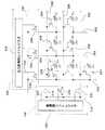
図12に指紋検出センサ40の一例を示す。この指紋検出センサ40は、本出願人により出願された特願2002−58071号に開示されたものと同じである。図12において、M本(Mは2以上の整数)の電源線200と、N本(Nは2以上の整数)の出力線202とを有する。M本の電源線200とN本の出力線202の各交点には静電容量検出素子204が設けられている。図12に示す静電容量検出素子204は、指が接触した時の閉回路として図示されており、指の凹凸パターンに依存して変化する可変容量CFと、信号増幅素子例えば信号増幅MIS型薄膜半導体装置(以下信号増幅用TFTと略記する)206とを有する。静電容量検出素子204に指が接触していない時には、可変容量CFの接地端側はオープン状態である。なお、可変容量CFについては後述する。
【0074】
M本の電源線200の各々は、対応する行に沿って配列されたN個の信号増幅用TFT206のドレインDに接続されている。また、M本の電源線200の各々は、M個の電源用パスゲート210の各々を介して共通電源線212に接続されている。すなわち、電源用パスゲート210はMIS型薄膜半導体装置にて形成され、そのソースSは電源線200に接続され、そのドレインDは共通電源線212に接続されている。電源選択回路220内には、上述のM個の電源用パスゲート210及び共通電源線212に加えて、電源用シフトレジスタ222が設けられている。電源用シフトレジスタ222の電源選択用出力線224に、M個の電源用パスゲート210の各ゲートGが接続されている。
【0075】
N本の出力線202各々は、対応する列に沿って配列されたM個の信号増幅用TFT206のソースSに接続されている。また、N本の出力線202の各々は、N個の出力信号用パスゲート230の各々を介して共通出力線232に接続されている。すなわち、出力信号用パスゲート230はMIS型薄膜半導体装置にて形成され、そのドレインDは出力線202に接続され、そのソースSは共通出力線232に接続されている。出力信号選択回路240内には、上述のN個の出力信号用パスゲート230及び共通出力線232に加えて、出力信号用シフトレジスタ242が設けられている。出力信号用シフトレジスタ242の出力選択用出力線244に、出力信号用パスゲート230のゲートGが接続されている。
【0076】
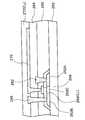
図13は、図12に示す静電容量検出素子204の断面図であり、指が接触されていない状態が図示されている。この静電容量検出素子204は、上述の信号増幅素子である信号増幅用TFT206に加えて、信号検出素子208を有する。
【0077】
図13において、絶縁層250上には、ソース領域252A、ドレイン領域252B及びその間のチャネル領域252Cを有する半導体膜252が形成されている。半導体膜252上にはゲート絶縁膜254が形成され、このゲート絶縁膜254を挟んでチャネル領域252Cと対向する領域にゲート電極256が形成されている。この半導体膜252、ゲート絶縁膜254及びゲート電極256で、信号増幅用TFT206が構成される。なお、電源用パスゲート210及び出力信号用パスゲート230も、信号増幅用TFT206と同様にして形成される。
【0078】
この信号用TFT206は第一層間絶縁膜260により被われている。第一層間絶縁膜260上には、図12に示す出力線202に相当する第一配線層262が形成されている。この第一配線層262は信号用TFT206のソース領域252Aに接続されている。
【0079】
第一配線層262は第二層間絶縁膜264により被われている。この第二層間絶縁膜264上には、図12に示す電源線200に相当する第二配線層266が形成されている。この第二配線層266は、信号増幅用TFT206のドレイン領域252Bに接続されている。なお、図13とは異なる構造として、第二配線層266を第一層間絶縁膜260上に形成し、第一配線層262を第二層間絶縁膜264上に形成してもよい。
【0080】
第二層間絶縁膜264上にはさらに、容量検出電極270が形成され、それを被って容量検出誘電体膜272が形成されている。容量検出誘電体膜272は、指紋検出センサ40の最表面に位置して保護膜としても機能し、この容量検出誘電体膜272に指が接触される。この容量検出電極270及び容量検出誘電体膜272により、信号検出素子208が構成される。
【0081】
(指紋検出動作)
指紋検出は、図13に示す容量検出誘電体膜272に指を接触させることで実施される。このとき、指紋検出センサ40の起動スイッチ(例えば感圧スイッチ)42が作動し、カード型情報記録媒体100内の電源が作動して、自動的に、指紋検出センサ40に電源が供給される。あるいは、カード型情報記録媒体100を図2の情報処理装置110にセットし、情報処理装置110の給電部112より電源が供給されても良い。
【0082】
本実施形態では、図12に示すM本のうち選択された1本の電源線200に電源電圧を供給し、かつ、そのときの信号を、N本のうち選択された1本の出力線202から検出することで、M×N個の静電容量検出素子204から順次信号を取り出している。
【0083】
指紋検出動作は大別して、(1)指紋パターンの山(凸部)が容量検出誘電体膜272に接触する場合と、(2)指紋パターンの谷(凹部)が容量検出誘電体膜272に対向する場合とがある。
【0084】
(1)指紋パターンの山(凸部)が容量検出誘電体膜272に接触する場合
図14に、この場合の静電容量検出素子204の等価回路を示す。符号300は人体の指紋の山に相当し、図13の容量検出電極270と誘電体膜272を挟んで対向する接地電極300が形成されている。ここで、電源電圧Vddは共通電源線212より供給される。符号CTは、信号増幅用TFT206のトランジスタ容量であり、符号CDは検出電極270と接地電極(指)300との間の容量である。
【0085】
ここで、信号増幅用TFT206のゲート電極長をL(μm)、ゲート電極幅をW(μm)、ゲート絶縁膜の厚みをtox(μm)、ゲート絶縁膜の比誘電率をεox、真空の誘電率をεoとする。このとき、トランジスタ容量CTは、
CT=εo・εox・L・W/tox
となる。
【0086】
また、容量検出電極270の面瀬S(μm2)、容量検出誘電体膜272の厚みをtd(μm)、容量検出誘電体膜の比誘電率をεdとする。このとき、容量CDは、
CD=εo・εd・S/td
となる。
【0087】
図14の等価回路において、信号増幅用TFT206のゲートに印加される電圧VGTは、
VGT=Vdd/(1+CD/CT)…(1)
となる。
【0088】
容量CDをトランジスタ容量CTよりも充分に大きく設定しておけば(例えばCD>10×CT)、(1)式の分母は無限大となり、
VGT≒0…(2)
と近似される。
【0089】
この結果、信号増幅用TFT206は、そのゲートにほとんど電圧がかからないためオフ状態となる。よって、信号増幅用TFT206のソース−ドレイン間に流れる電流Iは極めて小さくなる。この電流Iを測定することで、測定箇所が指紋パターンの山(凸部)であることが判定できる。
【0090】
(2)指紋パターンの谷(凹部)が容量検出誘電体膜272に対向する場合
図15に、この場合の静電容量検出素子204の等価回路を示す。符号302が人体の指紋の谷に相当する。この場合は、図14図に示す容量CDに加えて、誘電体膜272と指紋の谷との間に、空気を誘電体とする新たな容量CAが形成される。
【0091】
図15の等価回路において、信号増幅用TFT206のゲートに印加される電圧VGVは、
VGV=Vdd/{[1+(1/CT)]×1/[(1/CD)+(1/CA)]}…(3)
となる。
【0092】
容量CDをトランジスタ容量CTよりも充分に大きく設定しておけば(例えばCD>10×CT)、(3)式は、
VGV≒Vdd/[1+(CA/CT)]…(4)
と近似される。
【0093】
さらに、トランジスタ容量CTを、指紋の谷により形成される容量CAよりも充分に大きくしておけば(例えばCT>10×CA)、(4)式は、
VGV≒Vdd…(5)
と近似される。
【0094】
この結果、信号増幅用TFT206は、そのゲートに電源電圧Vddがかかるためオン状態となる。よって、信号増幅用TFT206のソース−ドレイン間に流れる電流Iは極めて大きくなる。この電流Iを測定することで、測定箇所が指紋パターンの谷(凹部)であることが判定できる。
【0095】
このように、図12に示す可変容量CFは、指紋の山が容量検出誘電体膜272に接触した時は容量CDとなり、指紋の谷が容量検出誘電体膜272に対向としたときは容量CDと容量CAとの和となり、指紋の凹凸に従って容量が変化する。この指紋の凹凸に従った容量変化に基づく電流を検出することで、指紋の山または谷を検出できる。
【0096】
以上の動作を、M×N個の静電容量検出素子204にて時分割で実施することで、指紋パターンを検出することが可能となる。
【0097】
ここで、電源電圧Vddに正電源を用いる場合には、ゲート電圧がゼロ近傍でドレイン電流が流れないエンハンスメント型N型トランジスタにて、信号増幅用TFT206を形成すればよい。CD>10×CTを満たす場合には、信号増幅用TFT206の伝達特性におけるドレイン電流が最小値となるゲート電圧(最小ゲート電圧)をVminとしたとき、0<Vmin<0.1×Vddを満たせばよい。
【0098】
電源電圧Vddに負電源を用いる場合には、ゲート電圧がゼロ近傍でドレイン電流が流れないエンハンスメント型P型トランジスタにて、信号増幅用TFT206を形成すればよい。CD>10×CTを満たす場合には、信号増幅用TFT206の伝達特性におけるドレイン電流が最小値となるゲート電圧(最小ゲート電圧)をVminとしたとき、0.1×Vdd<Vmin<0を満たせばよい。
【0099】
(指紋検出センサ・脈波検出センサを内蔵するカードの構造)
本実施形態のカード型情報記録媒体100は、図16に示すように、上述の指紋検出センサ40を含む第1の薄膜ディバイス400と、上述の脈波検出センサ50を含む第2の薄膜ディバイス410とを、柔軟性のある材質例えば樹脂などのカードベース基板420上に積層することで形成できる。
【0100】
ただし、これら第1,第2の薄膜ディバイス400,410を、直接にカードベース基板420上に形成することは困難である。
【0101】
そこで、指紋検出センサ40は先ず、図16に示すように、例えば第1製造基板430上に形成される。その一例として、第1製造基板430をガラス基板とした時には、その上に形成したアモルファスシリコン層をレーザ結晶化して多結晶シリコン層とし、それにより図13の半導体膜252を形成できる。その後は、通常の薄膜半導体製造プロセスを実施することで、第1製造基板420上に、指紋検出センサ40を含む第1の薄膜ディバイス400が形成される。
【0102】
脈波検出センサ50を含む第2の薄膜ディバイス410は、図16に示すように、例えば第2製造基板440上に形成される。特開平9−27611号などでは、面発光型半導体レーザ及びフォトダイオードが半導体基板上に形成されるので、その製法を利用すれば第2製造基板440は半導体基板である。
【0103】
これら第1,第2の薄膜ディバイス400,410は、本願出願人による転写技術(特開平10−125931、特開平10−177187、特開平11−20360、特開平11−26733、特開平11−26734、特開平11−74533、特開平11−312811)を用いて、カードベース基板420に転写される。
【0104】
ここで、第1,第2の薄膜ディバイス400,410は、その上下面の向きを維持した状態で、カードベース基板420に転写される必要がある。そこで、第1製造基板430及び第1の薄膜ディバイス400は一旦、第3製造基板450に接合され、その後第1製造基板430が剥離される。同様に、第2製造基板440及び第2の薄膜ディバイス400は一旦、第4製造基板460に接合され、その後第2製造基板440が剥離される。次に、第4製造基板460及び第2の薄膜ディバイス410がカードベース基板420に転写され、その後第4製造基板460が剥離される。最後に、第3製造基板450及び第1の薄膜ディバイス400が第2の薄膜ディバイス410上に転写され、その後第3製造基板450が剥離される。
【0105】
こうして、カードベース基板420上に第1,第2の薄膜ディバイス400,410が積層される。このとき、指紋検出センサ40の裏に脈波検出センサ50を配置することができ、更に容量検出電極270をインジウム酸化物(ITO)の様な透明導伝材料で形成するのが好ましい。こうすると、指紋検出センサ40の容量検出誘電体膜272に指をさせれば、その同一の指より指紋と脈波とを検出することができる。こうすると、指紋及び脈波の双方を偽造することが極めて困難となるので、本人照合の信頼性がより増大する。
【0106】
このように、指紋検出センサ40の裏に脈波検出センサ50を配置する場合には、指紋検出センサ40の構成部材が、脈波検出センサ40からの発光波長に対して透明である必要がある。このために、図13に示す第1,第2配線層262,266及び容量検出電極270を透明電極(例えばITO)にて形成すればよい。
【0107】
なお、本発明は上述の実施形態に限定されるものではなく、本発明の要旨の範囲内で種々の変形実施が可能である。例えば、本発明の本人照合装置は必ずしもカード型情報記録媒体に限らず、他の携帯型電子機器、設置型電子機器などに搭載しても良い。
【図面の簡単な説明】
【図1】 図1(A)〜図1(C)は、本発明の実施形態に係るカード型情報記録媒体の概略説明図である。
【図2】 図2(A)及び図2(B)は、図1(A)〜図1(C)とは異なる本発明の実施形態に係るカード型情報記録媒体の概略説明図である。
【図3】 本発明の実施形態に係るカード型情報記録媒体及び情報処理装置から構成される情報処理システムのブロック図である。
【図4】 本発明の実施形態に係るカード型情報記録媒体に内蔵される本人照合装置のブロック図である。
【図5】 脈拍の1拍について、脈波の波形の特徴を説明するための波形図である。
【図6】 図5に示す複数の変化点に関する指標を抽出する指標抽出部の一例を示すブロック図である。
【図7】 図5に示す複数の変化点に関する指標を抽出する指標抽出部の他の例を示すブロック図である。
【図8】 図8(A)は検出された脈波の原波形、図8(B)は図8(A)の速度波形、図8(C)は図8(A)の加速度波形をそれぞれ示す波形図である。
【図9】 加速度波形の特徴を説明するための概略説明図である。
【図10】 図7に示す加速度波形中の複数の変化点の波高比率を指標として抽出する指標抽出部のブロック図である。
【図11】 図3に示す本人照合装置の動作フローチャートである。
【図12】 指紋検出センサの概略説明図である。
【図13】 図12に示す容量検出素子の断面図である。
【図14】 指紋検出センサの誘電体膜に指紋の山を接触させた時の静電容量検出素子の等価回路図である。
【図15】 指紋検出センサの誘電体膜に指紋の谷を接触させた時の静電容量検出素子の等価回路図である。
【図16】 転写技術を利用したカード型情報記録媒体の製造工程を簡略的に示す概略説明図である。
【図17】 図11のステップ7にて一致と判断された指標データXiとその移動平均[Xi]との相関を示す特性図である。
【符号の説明】
10 基板、 12 メモリ、 14 CPU、 16 I/O、
20 表示部、 22 表示駆動部、 24 電源(太陽電池)、
30 本人照合装置、 40 指紋検出センサ、 50 脈波検出センサ、
52 指標抽出部、 54 時間比率抽出部、 55 加速度波形演算部、
56 波高比率抽出部、 58 履歴情報記憶部、 60 更新部、
70 照合部、 80 比較情報記憶部、 82 第1の比較情報記憶部、
84 第2の比較情報記憶部、 90 パスワード出力部、
100 カード型情報記録媒体、 110 情報処理装置(端末機器)、
112 給電部、 120 ホスト機器、 130 履歴情報記憶部、
140 情報更新部、 200 電源線、 202 出力線、
204 静電容量検出素子、
206 信号増幅素子(信号増幅用MIS型薄膜半導体装置)、
208 信号検出素子、 210 電源用パスゲート、 212 共通電源線、
220 電源選択回路、 222 電源用シフトレジスタ、
224 電源選択用出力線、 230 出力信号用パスゲート、
232 共通出力線、 240 出力信号選択回路、
242 出力信号用シフトレジスタ、 244 出力選択用出力線、
250 絶縁基板、 252 半導体膜、 252A ソース領域、
252B ドレイン領域、 252C チャネル領域、
260 第一層間絶縁膜、 262 第一配線層、 264 第二層間絶縁膜、
266 第二配線層、 270 容量検出電極、 272 容量検出誘電体膜、
300 指紋の山、 302 指紋の谷、 400 第1の薄膜ディバイス、
410 第2の薄膜ディバイス、 420 カードベース基板、
430 第1製造基板、 440 第2製造基板、 450 第3製造基板、
460 第4製造基板[0001]
BACKGROUND OF THE INVENTION
The present invention relates to an identity verification device, a card type information recording medium, and an information processing system using the same.
[0002]
[Background]
A technique using a fingerprint detection sensor for personal verification has been proposed. A resistance-sensitive fingerprint detection sensor (for example, see Patent Document 1), a photoelectric fingerprint detection sensor (for example, see Patent Document 2), and a piezoelectric device. A fingerprint sensor (for example, refer to Patent Document 3) and a capacitive fingerprint detection sensor (for example, refer to Patent Document 4) have been proposed.
[0003]
[Patent Document 1]
JP-A-3-6791
[Patent Document 2]
JP-A-4-271477
[Patent Document 3]
JP-A-5-61965
[Patent Document 4]
JP-A-11-118415
[0004]
[Background Art and Problems to be Solved by the Invention]
However, if relying solely on fingerprints for collation is not possible, the fingerprint can be collected even if the person is not alive.
[0005]
Japanese Patent Application Laid-Open No. 2001-184490 discloses a technique for engineeringly reading a fingerprint of a finger scanned on a reading roller and detecting a pulse with a pulse sensor provided in the vicinity thereof. However, since the pulse is a pulse, it is easy to forge. Further, since the reading roller is used for fingerprint detection, it is impossible to adopt the structure for a portable card, for example.
[0006]
SUMMARY OF THE INVENTION An object of the present invention is to provide a personal verification device that has a high personal verification accuracy and that makes it extremely difficult to forge a verification target, and a card-type information recording medium and information processing system using the same.
[0007]
[Means for Solving the Problems]
An identity verification apparatus according to one aspect of the present invention includes a first detection unit that detects operator's unique information, a second detection unit that detects the operator's pulse wave, and the second detection unit. Processing means for processing the detected pulse wave to extract at least one index, first storage means for storing first comparison information to be compared with the specific information, and the at least one index Second storage means for storing second comparison information to be compared with, and based on a comparison result between the unique information and the first comparison information, the operator is matched with the registered person, and A collation that outputs a signal indicating that the operator is authentic when it is determined that the operator is alive based on a comparison result between the at least one index and the second comparison information. Means. The signal indicating authenticity may be display information, an encrypted password, or a password may be output as an electronic signal.
[0008]
Here, the operator's unique information includes a fingerprint, an iris, a tooth profile, a hand, a face, a voiceprint, and the like, but the unique information detected by the first detection means is preferably a fingerprint. Such unique information is suitable for personal identification, but can be collected even if the operator is not a living body. Therefore, the second detection means detects a pulse wave emitted only from a surviving operator. The detected pulse wave is processed, and the index is extracted from the pulse wave by the index extraction unit. The shape of the pulse wave is unique to the surviving human, and the index extracted from the pulse wave is also specific to the surviving human. By indexing in this way, comparison with known stored information becomes easy. In this regard, when a pulse such as a pulse, which is one component of the component, is detected directly instead of the pulse wave itself, such a pulse can be artificially generated. On the other hand, it is extremely difficult to forge the pulse wave waveform, and it is almost impossible to forge any index in the pulse wave. Therefore, according to one aspect of the present invention, the personal verification accuracy is greatly improved, and the reliability of the personal verification result is improved.
[0009]
In one aspect of the present invention, the index extraction means can be configured in the following various forms. The index extraction unit is configured to detect a pulse wave detected by the second detection unit.Maximum (change from increase to decrease) or minimum (change from decrease to increase)pluralChanging pointA wave height extracting unit that extracts at least one wave height of the at least one wave as the at least one index may be included. Alternatively, the index extraction unit may detect a pulse wave detected by the second detection unit.Maximum or minimumpluralChanging pointThe time extraction part which extracts the time until it reaches at least one as said at least 1 parameter | index can be included. Alternatively, the index extraction unit may detect a pulse wave detected by the second detection unit.Maximum or minimumpluralChanging pointA wave height ratio extracting unit for extracting the wave height ratio as the at least one index may be included. Alternatively, the index extraction unit includes a calculation unit that calculates an acceleration waveform of the pulse wave detected by the second detection unit, and the acceleration waveformMaximum or minimumpluralChanging pointA wave height ratio extracting unit for extracting the wave height ratio as the at least one index may be included. Alternatively, the index extraction means is the pulse wave detected by the second detection means.Maximum or minimumpluralChanging pointA time ratio extraction unit that extracts a time ratio between them as the at least one index may be included. In this case, the time ratio extraction unit can extract the ratio between the period of the pulse wave and the ejection time from the pulse wave detected by the second detection means. Alternatively, the index extraction means can be an amplifier that amplifies the pulse wave detected by the second detection means. This amplifier extracts, as an index, an amplification factor when the pulse wave is amplified to a signal having a certain amplitude or more by an auto gain control function. The amplification factor as the index can be personal information of the living body equivalent to the blood vessel age.
[0010]
In one aspect of the present invention, a history information storage unit that stores history information of the at least one index extracted by the index extraction unit, and a second storage unit that stores the history information based on the history information. And an information updating unit for updating the second comparison information. By updating the second comparison information based on the history information, for example, the second comparison information is changed according to an index that changes over time, or the allowable range of comparison is narrowed based on the history information. can do.
[0011]
When the unique information is a fingerprint in one aspect of the present invention, the first detection means is a fingerprint detection sensor, and the fingerprint information of the person is stored in the first storage means.
[0012]
The fingerprint detection sensor can detect a fingerprint by detecting a capacitance that changes according to the unevenness of the operator's finger.
[0013]
Such a fingerprint detection sensor includes M (M is an integer of 2 or more) rows of power lines, N (N is an integer of 2 or more) columns of output lines, and M rows and N columns of power lines and output lines. It is possible to include M × N capacitance detection elements provided at each intersection.
[0014]
Each of the M × N capacitance detection elements includes a signal detection element and a signal amplification element, and the signal detection element includes a capacitance detection electrode and a capacitance detection dielectric film. The signal amplification MIS thin film semiconductor device having a gate electrode, a gate insulating film, and a semiconductor film can be used.
[0015]
Here, the fingerprint detection sensor may further include a power selection circuit connected to the M rows of power lines. The power supply selection circuit includes M power supply pass gates provided between a common power supply line and the M rows of power supply lines, and each of the M power supply pass gates includes a gate electrode and a gate insulating film. And a signal amplifying MIS thin film semiconductor device having a semiconductor film.
[0016]
Furthermore, the fingerprint detection sensor may further include a signal selection circuit connected to the N rows of signal lines. The signal selection circuit includes N output signal pass gates provided between a common output line and the N columns of output lines, and each of the N output signal pass gates includes a gate electrode and a gate. It can be formed by a MIS thin film semiconductor device for signal amplification having an insulating film and a semiconductor film.
[0017]
In one aspect of the present invention, the apparatus may further include an activation switch that activates the personal verification device by detecting a finger contact with the fingerprint detection sensor.
[0018]
In one aspect of the present invention, the second detection means includes a pulse wave detection sensor having a light emitting element and a light receiving element, and can optically detect the pulse wave of the operator. In this case, the second detection means includes a pulse wave detection sensor having a light emitting element and a light receiving element, and the fingerprint detection sensor and the pulse wave detection sensor are arranged such that the fingerprint detection sensor is located on the surface side. And a region where the fingerprint detection sensor intersects the light emission path from the light emitting element and the light reception path to the light receiving element is formed by a member transparent to the light emission wavelength from the light emitting element. Can do.
[0019]
Here, when the collation means determines that the fingerprint detected by the fingerprint detection sensor is not authentic, the pulse wave detection by the pulse wave detection sensor can be prohibited. Thereby, an optical pulse wave inspection that consumes a relatively large amount of electric power can be omitted.
[0020]
A low-frequency cutoff filter that blocks a low-frequency component from the pulse wave detected by the pulse wave detection sensor can be further provided. The low frequency band includes frequency components that reflect autonomic nervous system functions such as sympathetic nervous system functions or parasympathetic nervous system functions, and frequency components that originate from body movements, so these must be removed. Because. In particular, in this low-frequency cutoff filter, the low-frequency cutoff frequency is preferably set to a value in the range of 0.4 to 0.5 Hz. This is because only the useless frequency components as described above can be removed, and the characteristics of the pulse wave waveform are not impaired.
[0021]
An identity verification apparatus according to another aspect of the present invention includes a detection unit that detects biological information of an operator that changes over time, a first storage unit that stores comparison information to be compared with the biological information, Based on history information stored in the second storage means and second storage means for storing history information of the biological information detected by the detection means, the comparison information in the first storage means is updated. And updating means for outputting and a matching means for outputting a signal indicating that the operator is authentic based on a comparison result between the biological information and the comparison information.
[0022]
Here, biological information can include pulse wave, brain wave, electrocardiogram, myoelectricity, body surface temperature, radiant heat from the body surface, etc. Preferably, it can be mentioned. Especially in the acceleration waveform of pulse waveChanging pointThe wave height ratio is age-dependent. Thus, the comparison information compared with the biological information that changes with time needs to be updated according to the passage of time. In another aspect of the present invention, each time biometric information is detected, it is stored as history information, and the comparison information is updated based on the history information. Since the comparison information is automatically updated in this way, the personal verification device having the automatic update function can be used semipermanently. As the comparison information, a moving average value of the biological information and a deviation indicating a deviation degree of the biological information from the moving average value are used. The next moving average value is estimated from the latest moving average of the past several times, and a value of k times the deviation (1 ≦ k ≦ 3) around the estimated value is set as the allowable range of the next biological information. By doing so, it is possible to significantly reduce the mistaken rejection of the person and others and to prevent unauthorized use due to pulse wave forgery.
[0023]
A card type information recording medium according to still another aspect of the present invention incorporates the above-described personal verification device.
[0024]
In particular, a card-type information recording medium having an identity verification device provided with a pulse wave detection sensor on the back of a fingerprint detection sensor includes at least a first thin film device on which the pulse wave detection sensor is formed, and at least the fingerprint detection sensor. The formed second thin film device can be laminated.
[0025]
These card-type information recording media can further include a display unit for displaying that the card is ready for use based on the signal from the verification unit.
[0026]
An information processing system according to still another aspect of the present invention includes the above-described card type information recording medium and an information processing apparatus that performs processing based on information of the card type information recording medium. After the signal is input from the verification means, information other than the information used for the personal verification is read from the card type information recording medium.
[0027]
In this way, the personal information used for the personal verification is processed only inside the card-type information recording medium and does not leak outside.
[0028]
Here, the information processing apparatus may include a power supply unit that supplies power to the card type information recording medium. Of course, a power source may be built in the card type information recording medium.
[0029]
DETAILED DESCRIPTION OF THE INVENTION
Hereinafter, an embodiment in which the present invention is applied to a card type information recording medium incorporating a personal verification device and an information processing system using the same will be described with reference to the drawings.
[0030]
(Card type information recording medium)
For example, as an IC card including an integrated circuit (IC), a memory card, an I / O (input / output circuit) card, an ISO-compliant card, and the like are known. In the present embodiment, a personal verification device is incorporated in various cards used as these credit cards, cash cards and the like.
[0031]
As an example, an example of the card type information recording medium of the present embodiment is shown in FIGS. 1 (A) to 1 (C) and FIGS. 2 (A) and 2 (B). The card shown in FIG. 1A has a
[0032]
Here, the
[0033]
(Information processing system)
FIG. 3 shows an information processing system including a card type
[0034]
The
[0035]
In any case, since the card-type
[0036]
(Person verification device)
FIG. 4 is a block diagram of the
[0037]
An
[0038]
Fingerprint information from the
[0039]
The
[0040]
(Pulse wave detection sensor and index extraction unit)
Although the pulse
[0041]
The emission wavelength from the light emitting element is preferably selected in the vicinity of the absorption wavelength peak of hemoglobin in blood. Since the light reception level changes according to the blood flow volume, a pulse wave (for example, volume pulse wave) waveform can be detected. As such a light-emitting element, an InGaN-based (indium-gallium-nitrogen-based) blue LED or the like can be used, and an emission wavelength is 350 to 600 nm (a peak wavelength is around 450 nm). As the light receiving element, for example, a GaAsP-based (gallium-arsenic-phosphorus-based) phototransistor can be used, and the main sensitivity region is 300 to 600 nm. In addition, light with a wavelength of 700 nm or less among external light tends to be difficult to transmit through the finger tissue. Therefore, even if a pulse wave is detected with a finger in contact with the card, a high S / N can be secured.
[0042]
Considering the incorporation of the pulse
[0043]
FIG. 5 shows a waveform for one beat of the pulse wave detected by the pulse
(1) Sequentially one pulse waveMultiple change points that are maximal or maximalP1 to P5 appear.
(2)Changing pointP1 to P5 have wave heights y1 to y5.
(3) Each pulse wave start time t0 as a referenceChanging pointThe time until P1 to P5 appears is T1 to T5, and the elapsed time (cycle) until the next one-beat pulse wave starts is T6.
[0044]
In this embodiment, suchChanging pointAt least one of wave heights y1 to y5 of P1 to P5, or from time t0Changing pointThe
[0045]
Such a pulse wave is a biological signal emitted from a living body, and an index extracted by processing it is unique to the living body. Therefore, if such an index can be extracted, it is proved that the finger of the cardholder who surely survives is not monitored, but the finger of the cut card is monitored. In this regard, when it is intended to directly detect a pulse (that is, a period) such as a pulse, which is one component thereof, instead of the pulse wave itself, such a pulse can be artificially generated. In this embodiment, a pulse wave that is artificially difficult to counterfeit is detected, and an index extracted by processing the pulse wave is compared. Therefore, theft of the card is reliably prevented.
[0046]
The index described above can be extracted by the
[0047]
The low-
[0048]
The
[0049]
Instead of FIG. 6, an
[0050]
8A is an original waveform of the detected pulse wave, FIG. 8B is a velocity waveform (first derivative waveform) of FIG. 8A, and FIG. 8C is an acceleration waveform (FIG. 8A). It is a wave form diagram which shows each (secondary differential waveform). The acceleration waveform in FIG. 8C is more clear as shown in FIG.Changing pointa to e. Therefore, the acceleration waveformChanging pointany two of aeChanging pointThe wave height ratio can also be used as an indicator.
[0051]
As such a wave height ratio, for example, the ratios b / a, c / a, d / a, e / a of the first maximum point a and the first minimum point b appearing in the secondary collection waveform of the pulse wave are as follows: It is an index that changes depending on age. Among these, the wave height ratios b / a and d / a are particularly suitable as a biometric index for cardholders of various ages because the age-dependent rate is significant, and the collation accuracy is improved. Some of these indicators reflect the gender of men and women and can be used for gender checks.
[0052]
Such a wave height ratio can be extracted by the
[0053]
Examples of other indicators include the following. That is, in the light transmission path between the light emitting element and the light receiving element of the pulse
[0054]
Therefore, in this case, the amplifier that amplifies the output of the pulse
[0055]
(Operation on the personal verification device)
FIG. 11 is an operation flowchart of the
[0056]
The detected fingerprint information is input to the
[0057]
Here, if the determination in
[0058]
If the fingerprint information does not match, the subsequent verification operation is not performed. Here, for fingerprint detection, as described later, for example, if the detection principle of electrostatic capacitance is used, less power is consumed. On the other hand, if pulse waves are detected optically as described above, a relatively large amount of power is consumed. Therefore, when the fingerprints do not match, the pulse wave detection operation with high power consumption is not performed.
[0059]
If the determination in
[0060]
Thus, a pulse wave is a biological signal emitted from a living body, and an index extracted by processing it is unique to the living body. Therefore, if such an index matches the stored information, it is proved that the finger of the cardholder who surely survives is monitored. In addition, depending on the index, an age check and / or gender check can be performed to reflect the registered person's age, sex, and the like.
[0061]
If the determination in
[0062]
If the determination in
[0063]
(History information storage unit and information update unit)
As shown in FIG. 4, the
[0064]
Among the indexes extracted from the pulse wave, as described above, there are indexes that change with time, such as age dependency. For this reason, if a constant index is always stored as the second comparison information, it will differ from the person's index over time. Therefore, each time the determination of matching is made in the index comparison (YES in step 7), the extracted index is stored in the history
[0065]
[Expression 1]
[0066]
δi≡Xi-/ Xi
The N-square mean value of this deviation is expressed as variance σi2Call it.
[0067]
[Expression 2]
[0068]
[Equation 3]
[0069]
[Expression 4]
[0070]
Li + 1= [X]i + 1―Kσi
Similarly, the upper limit of the allowable range Ui + 1Is the next moving average estimate [X]i + 1Movement deviation σiK times (1 ≦ k ≦ 3).
[0071]
Ui + 1= [X]i + 1+ Kσi
Thus, the allowable range of the next extraction index data is Li + 1To Ui + 1This becomes the updated second comparison information. A value of about 1 to 3 is appropriate as the value of k. If k is larger than 1, the possibility of an error to reject the person can be reduced. If it is smaller than 3, the possibility of misidentifying others as the person can be reduced. It can be said that the ideal value of k is 1.5 or more and 2.5 or less. Measured value X of the next extraction index datai + 1Is Li + 1And Ui + 1If you are in between,
[X]i + 1―Kσi≦ Xi + 1≦ [X]i + 1+ Kσi
When the i + 1th use is satisfied, the index comparison step in FIG. 11 makes a determination of coincidence (YES in step 7) (see FIG. 17).
[0072]
Thus, the second comparison information compared with the index is updated to the latest information. Therefore, collation errors can be reduced.
[0073]
(Fingerprint detection sensor)
FIG. 12 shows an example of the
[0074]
Each of the M
[0075]
Each of the
[0076]
FIG. 13 is a cross-sectional view of the
[0077]
In FIG. 13, over the insulating
[0078]
The
[0079]
The
[0080]
A
[0081]
(Fingerprint detection operation)
Fingerprint detection is performed by bringing a finger into contact with the capacitance
[0082]
In the present embodiment, a power supply voltage is supplied to one
[0083]
Fingerprint detection operations are broadly divided into (1) a case where a peak (convex part) of a fingerprint pattern is in contact with the capacitance
[0084]
(1) When a crest (convex portion) of a fingerprint pattern contacts the capacitance
FIG. 14 shows an equivalent circuit of the
[0085]
Here, the gate electrode length of the
CT= Εo · εox · L · W / tox
It becomes.
[0086]
Further, the surface S of the capacitance detection electrode 270 (μm2), the thickness of the capacitance
CD= Εo · εd · S / td
It becomes.
[0087]
In the equivalent circuit of FIG. 14, the voltage V applied to the gate of the signal amplification TFT 206.GTIs
VGT= Vdd / (1 + CD/ CT) ... (1)
It becomes.
[0088]
Capacity CDTransistor capacity CT(For example, CD> 10 × CT), (1) denominator is infinite,
VGT≒ 0 ... (2)
Is approximated by
[0089]
As a result, the
[0090]
(2) When the valley (concave portion) of the fingerprint pattern faces the capacitance
FIG. 15 shows an equivalent circuit of the
[0091]
In the equivalent circuit of FIG. 15, the voltage V applied to the gate of the signal amplification TFT 206.GVIs
VGV= Vdd / {[1+ (1 / CT)] × 1 / [(1 / CD) + (1 / CA)]} ... (3)
It becomes.
[0092]
Capacity CDTransistor capacity CT(For example, CD> 10 × CT), (3)
VGV≒ Vdd / [1+ (CA/ CT]] ... (4)
Is approximated by
[0093]
Furthermore, transistor capacitance CT, The capacitance C formed by the valley of the fingerprintA(For example, CT> 10 × CA), (4)
VGV≈ Vdd (5)
Is approximated by
[0094]
As a result, the
[0095]
Thus, the variable capacitor C shown in FIG.FWhen the crest of fingerprint touches the capacitance detecting
[0096]
A fingerprint pattern can be detected by performing the above operation in a time-sharing manner with the M × N
[0097]
Here, when a positive power supply is used as the power supply voltage Vdd, the
[0098]
When a negative power supply is used for the power supply voltage Vdd, the
[0099]
(Structure of card with fingerprint detection sensor and pulse wave detection sensor)
As shown in FIG. 16, the card-type
[0100]
However, it is difficult to directly form the first and second
[0101]
Therefore, the
[0102]
As shown in FIG. 16, the second
[0103]
These first and second
[0104]
Here, the first and second
[0105]
Thus, the first and second
[0106]
As described above, when the pulse
[0107]
In addition, this invention is not limited to the above-mentioned embodiment, A various deformation | transformation implementation is possible within the range of the summary of this invention. For example, the personal verification device of the present invention is not necessarily limited to a card-type information recording medium, and may be mounted on other portable electronic devices, installed electronic devices, and the like.
[Brief description of the drawings]
FIG. 1 (A) to FIG. 1 (C) are schematic explanatory diagrams of a card type information recording medium according to an embodiment of the present invention.
2 (A) and 2 (B) are schematic explanatory views of a card type information recording medium according to an embodiment of the present invention different from FIGS. 1 (A) to 1 (C).
FIG. 3 is a block diagram of an information processing system including a card type information recording medium and an information processing apparatus according to an embodiment of the present invention.
FIG. 4 is a block diagram of a personal verification device built in a card type information recording medium according to an embodiment of the present invention.
FIG. 5 is a waveform diagram for explaining the characteristics of the pulse wave waveform for one pulse.
6 shows a plurality of pieces shown in FIG.Changing pointIt is a block diagram which shows an example of the parameter | index extraction part which extracts the parameter | index regarding.
FIG. 7 shows a plurality of pieces shown in FIG.Changing pointIt is a block diagram which shows the other example of the parameter | index extraction part which extracts the parameter | index regarding.
8A is an original waveform of a detected pulse wave, FIG. 8B is a velocity waveform of FIG. 8A, and FIG. 8C is an acceleration waveform of FIG. 8A. FIG.
FIG. 9 is a schematic explanatory diagram for explaining characteristics of an acceleration waveform.
FIG. 10 shows a plurality of acceleration waveforms shown in FIG.Changing pointIt is a block diagram of the parameter | index extraction part which extracts the wave height ratio as a parameter | index.
11 is an operation flowchart of the personal verification device shown in FIG. 3;
FIG. 12 is a schematic explanatory diagram of a fingerprint detection sensor.
13 is a cross-sectional view of the capacitance detection element shown in FIG.
FIG. 14 is an equivalent circuit diagram of a capacitance detection element when a fingerprint crest is brought into contact with a dielectric film of the fingerprint detection sensor.
FIG. 15 is an equivalent circuit diagram of a capacitance detection element when a fingerprint valley is brought into contact with a dielectric film of a fingerprint detection sensor.
FIG. 16 is a schematic explanatory diagram schematically showing a manufacturing process of a card type information recording medium using a transfer technique.
FIG. 17 is a characteristic diagram showing a correlation between index data Xi determined to be coincident in
[Explanation of symbols]
10 substrates, 12 memory, 14 CPU, 16 I / O,
20 display unit, 22 display drive unit, 24 power supply (solar cell),
30 person verification device, 40 fingerprint detection sensor, 50 pulse wave detection sensor,
52 index extraction unit, 54 time ratio extraction unit, 55 acceleration waveform calculation unit,
56 wave height ratio extraction unit, 58 history information storage unit, 60 update unit,
70 verification unit, 80 comparison information storage unit, 82 first comparison information storage unit,
84 second comparison information storage unit, 90 password output unit,
100 card type information recording medium, 110 information processing device (terminal device),
112 power supply unit, 120 host device, 130 history information storage unit,
140 information update unit, 200 power line, 202 output line,
204 capacitance detection element,
206 signal amplification element (MIS type thin film semiconductor device for signal amplification),
208 signal detection element, 210 pass gate for power supply, 212 common power supply line,
220 power supply selection circuit, 222 power supply shift register,
224 output line for power supply selection, 230 pass gate for output signal,
232 common output lines, 240 output signal selection circuit,
242 shift register for output signal, 244 output line for output selection,
250 insulating substrate, 252 semiconductor film, 252A source region,
252B drain region, 252C channel region,
260 first interlayer insulating film, 262 first wiring layer, 264 second interlayer insulating film,
266 second wiring layer, 270 capacitance detection electrode, 272 capacitance detection dielectric film,
300 fingerprint ridge, 302 fingerprint valley, 400 first thin film device,
410 second thin film device, 420 card base substrate,
430 1st manufacturing substrate, 440 2nd manufacturing substrate, 450 3rd manufacturing substrate,
460 Fourth production substrate
Claims (22)
Translated fromJapanese前記操作者の脈波を検出する第2の検出手段と、
前記第2の検出手段にて検出された脈波を処理して、少なくとも一つの指標を抽出する指標抽出手段と、
前記固有情報と比較される第1の比較情報を記憶する第1の記憶手段と、
前記少なくとも一つの指標と比較される第2の比較情報を記憶する第2の記憶手段と、
前記固有情報と前記第1の比較情報との比較結果に基づいて、前記操作者が登録された本人と一致され、かつ、前記少なくとも一つの指標と前記第2の比較情報との比較結果に基づいて、前記操作者が生存していると判断された時に、前記操作者が真正であることを示す信号を出力する照合手段と、
を有し、
前記固有情報は指紋であり、前記第1の検出手段は前記操作者の指の凹凸に応じて変化する静電容量を検出する指紋検出センサであり、前記第1の記憶手段には本人の指紋情報が記憶され、
前記第2の検出手段は、発光素子と受光素子とを有する脈波検出センサを含み、
前記指紋検出センサが表面側に位置するようにして、前記指紋検出センサと前記脈波検出センサとが積層され、かつ、前記指紋検出センサが前記発光素子からの発光経路及び前記受光素子への受光経路と交差する領域は、前記発光素子からの発光波長に対して透明な部材により形成されている本人照合装置。First detection means for detecting the operator's unique information;
Second detection means for detecting the pulse wave of the operator;
Index extraction means for processing the pulse wave detected by the second detection means to extract at least one index;
First storage means for storing first comparison information to be compared with the unique information;
Second storage means for storing second comparison information to be compared with the at least one index;
Based on the comparison result between the unique information and the first comparison information, the operator is matched with the registered person, and based on the comparison result between the at least one index and the second comparison information. And a collating means for outputting a signal indicating that the operator is authentic when it is determined that the operator is alive,
Have
The unique information is a fingerprint, the first detection means is a fingerprint detection sensor that detects a capacitance that changes in accordance with the unevenness of the operator's finger, and the first storage means has a fingerprint of the person in question. Information is remembered,
The second detection means includes a pulse wave detection sensor having a light emitting element and a light receiving element,
The fingerprint detection sensor and the pulse wave detection sensor are stacked such that the fingerprint detection sensor is positioned on the surface side, and the fingerprint detection sensor receives a light emission path from the light emitting element and light reception to the light receiving element. The area | region which cross | intersects a path | route is the personal verification apparatus currently formed with the member transparent with respect to the light emission wavelength from the said light emitting element.
前記指標抽出手段は、前記第2の検出手段にて検出された脈波が極大または極小となる複数の変化点の少なくとも一つの波高を、前記少なくとも一つの指標として抽出する波高抽出部を含む本人照合装置。In claim 1,
The index extraction means includes a wave height extraction section that extracts at least one wave height of a plurality ofchange points at which the pulse wave detected by the second detection means ismaximum or minimum as the at least one index. Verification device.
前記指標抽出手段は、前記第2の検出手段にて検出された脈波が極大または極小となる複数の変化点の少なくとも一つに至るまでの時間を、前記少なくとも一つの指標として抽出する時間抽出部を含む本人照合装置。In claim 1 or 2,
The index extraction unit extracts a time until the pulse wave detected by the second detection unit reaches at least one of a plurality ofchange points at which the pulse wave becomesmaximum or minimum as the at least one index. Identity verification device including department.
前記指標抽出手段は、前記第2の検出手段にて検出された脈波が極大または極小となる複数の変化点の波高比率を、前記少なくとも一つの指標として抽出する波高比率抽出部を含む本人照合装置。In any one of Claims 1 thru | or 3,
The index extraction unit includes a pulse height ratio extraction unit that extracts a wave height ratio of a plurality ofchange points at which the pulse wave detected by the second detection unit ismaximum or minimum as the at least one index. apparatus.
前記指標抽出手段は、前記第2の検出手段にて検出された脈波の加速度波形を演算する演算部と、前記加速度波形が極大または極小となる複数の変化点の波高比率を、前記少なくとも一つの指標として抽出する波高比率抽出部を含む本人照合装置。In any one of Claims 1 thru | or 4,
The index extraction unit includes a calculation unit that calculates an acceleration waveform of the pulse wave detected by the second detection unit,and a wave height ratio of a plurality ofchange points at which the acceleration waveform ismaximized or minimized. Identity verification device that includes a crest ratio extraction unit that extracts as one index.
前記指標抽出手段は、前記第2の検出手段にて検出された脈波が極大または極小となる複数の変化点間の時間比率を、前記少なくとも一つの指標として抽出する時間比率抽出部を含む本人照合装置。In any one of Claims 1 thru | or 5,
The index extraction unit includes a time ratio extraction unit that extracts, as the at least one index, a time ratio between a plurality ofchange points at which the pulse wave detected by the second detection unit ismaximum or minimum. Verification device.
前記時間比率抽出部は、前記第2の検出手段にて検出された脈波より、該脈波の周期と駆出時間との比率を抽出するものである本人照合装置。In claim 6,
The identity verification device, wherein the time ratio extraction unit extracts a ratio between the period of the pulse wave and the ejection time from the pulse wave detected by the second detection means.
前記指標抽出手段は、前記第2の検出手段にて検出された脈波を増幅する増幅器であり、前記増幅器は、オート・ゲイン・コントロール機能により前記脈波を一定振幅以上の信号に増幅した時の増幅倍率を指標として抽出する本人照合装置。In claim 1,
The index extraction means is an amplifier that amplifies the pulse wave detected by the second detection means, and the amplifier amplifies the pulse wave to a signal having a certain amplitude or more by an auto gain control function. The person verification device which extracts the amplification factor of as an index.
前記指標抽出手段にて抽出された前記少なくとも一つの指標の履歴情報を記憶する履歴情報記憶部と、
前記履歴情報に基づいて、前記第2の記憶手段に記憶されている前記第2の比較情報を更新する情報更新部と、
をさらに含む本人照合装置。In any one of Claims 1 thru | or 8.
A history information storage unit that stores history information of the at least one index extracted by the index extraction means;
An information updating unit that updates the second comparison information stored in the second storage unit based on the history information;
A personal identification device further comprising:
前記指紋検出センサは、M(Mは2以上の整数)行の電源線と、N(Nは2以上の整数)列の出力線と、前記M行N列の電源線及び出力線の各交点にそれぞれ設けられたM×N個の静電容量検出素子とを含む本人照合装置。In any one of Claims 1 thru | or 9,
The fingerprint detection sensor includes M (M is an integer of 2 or more) rows of power lines, N (N is an integer of 2 or more) columns of output lines, and M rows and N columns of power lines and output lines. And a M × N electrostatic capacity detecting element provided in each.
前記M×N個の静電容量検出素子の各々は、信号検出素子と信号増幅素子とを含み、
前記信号検出素子は、容量検出電極と容量検出誘電体膜とを含み、
前記信号増幅素子は、ゲート電極、ゲート絶縁膜及び半導体膜を有する信号増幅用MIS型薄膜半導体装置にて形成されている本人照合装置。In claim 10,
Each of the M × N capacitance detection elements includes a signal detection element and a signal amplification element,
The signal detection element includes a capacitance detection electrode and a capacitance detection dielectric film,
The signal amplifying device is a personal verification device formed of a MIS type thin film semiconductor device for signal amplification having a gate electrode, a gate insulating film, and a semiconductor film.
前記M行の電源線に接続される電源選択回路をさらに有し、
前記電源選択回路は、共通電源線と前記M行の電源線との間に設けられたM個の電源用パスゲートとを含み、前記M個の電源用パスゲートの各々は、ゲート電極、ゲート絶縁膜及び半導体膜を有する信号増幅用MIS型薄膜半導体装置にて形成されている本人照合装置。In claim 11,
A power selection circuit connected to the M rows of power lines;
The power supply selection circuit includes M power supply pass gates provided between a common power supply line and the M rows of power supply lines, and each of the M power supply pass gates includes a gate electrode, a gate insulating film And a person verification device formed of a signal amplification MIS thin film semiconductor device having a semiconductor film.
前記N行の信号線に接続される信号選択回路をさらに有し、
前記電源選択回路は、共通出力線と前記N列の出力線との間に設けられたN個の出力信号用パスゲートとを含み、前記N個の出力信号用パスゲートの各々は、ゲート電極、ゲート絶縁膜及び半導体膜を有する信号増幅用MIS型薄膜半導体装置にて形成されている本人照合装置。In claim 11 or 12,
A signal selection circuit connected to the N rows of signal lines;
The power supply selection circuit includes N output signal pass gates provided between a common output line and the N columns of output lines, and each of the N output signal pass gates includes a gate electrode, a gate, A personal verification device formed of a signal amplification MIS thin film semiconductor device having an insulating film and a semiconductor film.
前記指紋検出センサへの指の接触を検知して、本人照合装置を起動させる起動スイッチをさらに有する本人照合装置。In any of claims 10 to 13,
A personal verification apparatus further comprising an activation switch for detecting contact of a finger with the fingerprint detection sensor and activating the personal verification apparatus.
前記指紋検出センサにて検出された指紋が真正でないと前記照合手段により判断された時は、前記脈波検出センサでの脈波の検出が禁止される本人照合装置。In any one of Claims 1 thru | or 14.
A personal verification device in which detection of a pulse wave by the pulse wave detection sensor is prohibited when the verification means determines that the fingerprint detected by the fingerprint detection sensor is not authentic.
前記脈波検出センサにて検出された脈波から低域周波数成分を遮断する低域遮断フィルタをさらに有する本人照合装置。In any one of Claims 1 thru | or 15,
The personal verification device further comprising a low-frequency cutoff filter that blocks low-frequency components from the pulse wave detected by the pulse wave detection sensor.
前記低域遮断フィルタは、低域遮断周波数が0.4〜0.5Hzの範囲中の値に設定されている本人照合装置。In claim 16,
The low-frequency cutoff filter is a personal verification device in which a low-frequency cutoff frequency is set to a value in a range of 0.4 to 0.5 Hz.
少なくとも前記脈波検出センサが形成された第1の薄膜ディバイスと、少なくとも前記指紋検出センサが形成された第2の薄膜ディバイスとが積層されているカード型情報記録媒体。The card-type information recording medium according to claim 18,
A card type information recording medium in which at least a first thin film device on which the pulse wave detection sensor is formed and a second thin film device on which at least the fingerprint detection sensor is formed are laminated.
前記照合手段からの前記信号に基づいて、カード使用可能状態であることを表示する表示部をさらに有するカード型情報記録媒体。In claim 18 or 19,
A card-type information recording medium further comprising a display unit for displaying that the card is ready for use based on the signal from the verification unit.
前記カード型情報記録媒体の情報に基づいて処理する情報処理装置と、
を有し、
前記情報処理装置は、前記照合手段から前記信号が入力された後に、前記カード型情報記録媒体から、本人照合に用いた情報以外の情報を読み取る情報処理システム。A card type information recording medium according to any one of claims 18 to 20,
An information processing apparatus for processing based on information of the card-type information recording medium;
Have
An information processing system in which the information processing apparatus reads information other than information used for personal verification from the card-type information recording medium after the signal is input from the verification unit.
前記情報処理装置は、前記カード型情報記録媒体に給電する給電部を有する情報処理システム。In claim 21,
The information processing apparatus is an information processing system having a power supply unit that supplies power to the card type information recording medium.
Priority Applications (3)
| Application Number | Priority Date | Filing Date | Title |
|---|---|---|---|
| JP2002325133AJP4366921B2 (en) | 2002-07-12 | 2002-11-08 | Personal verification device, card-type information recording medium, and information processing system using the same |
| US10/614,873US7302088B2 (en) | 2002-07-12 | 2003-07-09 | Personal verification device, card-type information storage medium, and information processing system using the same |
| CNB03149529XACN100449565C (en) | 2002-07-12 | 2003-07-14 | Retracting mechanism of optical element for retractable photographing lens |
Applications Claiming Priority (2)
| Application Number | Priority Date | Filing Date | Title |
|---|---|---|---|
| JP2002203991 | 2002-07-12 | ||
| JP2002325133AJP4366921B2 (en) | 2002-07-12 | 2002-11-08 | Personal verification device, card-type information recording medium, and information processing system using the same |
Publications (3)
| Publication Number | Publication Date |
|---|---|
| JP2004089675A JP2004089675A (en) | 2004-03-25 |
| JP2004089675A5 JP2004089675A5 (en) | 2005-12-15 |
| JP4366921B2true JP4366921B2 (en) | 2009-11-18 |
Family
ID=32072233
Family Applications (1)
| Application Number | Title | Priority Date | Filing Date |
|---|---|---|---|
| JP2002325133AExpired - Fee RelatedJP4366921B2 (en) | 2002-07-12 | 2002-11-08 | Personal verification device, card-type information recording medium, and information processing system using the same |
Country Status (3)
| Country | Link |
|---|---|
| US (1) | US7302088B2 (en) |
| JP (1) | JP4366921B2 (en) |
| CN (1) | CN100449565C (en) |
Families Citing this family (41)
| Publication number | Priority date | Publication date | Assignee | Title |
|---|---|---|---|---|
| JP4003750B2 (en) | 2003-04-17 | 2007-11-07 | セイコーエプソン株式会社 | Capacitance detection device |
| JP3858865B2 (en) | 2003-08-29 | 2006-12-20 | セイコーエプソン株式会社 | Capacitance detection device |
| JP4432625B2 (en) | 2003-09-05 | 2010-03-17 | セイコーエプソン株式会社 | Capacitance detection device |
| JP3909712B2 (en) | 2003-10-10 | 2007-04-25 | セイコーエプソン株式会社 | Capacitance detection device |
| JP2005233688A (en) | 2004-02-17 | 2005-09-02 | Seiko Epson Corp | Capacitance detection device, fingerprint sensor, biometric authentication device, and capacitance detection condition search method |
| US8030745B2 (en)* | 2004-03-04 | 2011-10-04 | Semiconductor Energy Laboratory Co., Ltd. | ID chip and IC card |
| US20060093192A1 (en) | 2004-11-03 | 2006-05-04 | Bechtel J S | Finger guide device |
| KR20060053812A (en)* | 2004-11-17 | 2006-05-22 | 삼성전자주식회사 | Biometric Recognition Apparatus and Method |
| DE102004061335A1 (en)* | 2004-12-20 | 2006-07-06 | Robert Bosch Gmbh | Method and system for acquiring biometric features |
| JP4567479B2 (en)* | 2005-02-04 | 2010-10-20 | セイコーインスツル株式会社 | Biological information measuring device and biological information measuring method |
| EP1851678A2 (en)* | 2005-02-08 | 2007-11-07 | Koninklijke Philips Electronics N.V. | Optical speckle pattern investigation |
| JP2006218033A (en)* | 2005-02-09 | 2006-08-24 | Univ Of Electro-Communications | Biometric identification method and biometric identification device |
| US20060294380A1 (en)* | 2005-06-28 | 2006-12-28 | Selim Aissi | Mechanism to evaluate a token enabled computer system |
| DE102005047754A1 (en)* | 2005-09-28 | 2007-04-05 | Fraunhofer-Gesellschaft zur Förderung der angewandten Forschung e.V. | Living person `s biometric characteristic e.g. skin lines, detecting method, involves recording part of fingerprint pattern of finger, and detecting cyclic change of size of part of fingerprint pattern |
| JP2007213196A (en)* | 2006-02-08 | 2007-08-23 | Olympus Corp | Personal authentication method, personal authentication system, and biological information measurement system |
| US7983451B2 (en)* | 2006-06-30 | 2011-07-19 | Motorola Mobility, Inc. | Recognition method using hand biometrics with anti-counterfeiting |
| JP4923910B2 (en)* | 2006-09-22 | 2012-04-25 | 富士通株式会社 | Biometric authentication device, control method, and control program |
| CN1987462B (en)* | 2006-12-26 | 2015-03-25 | 金政策 | Probe for detecting matrilinear inheritance chondriosome deafness gene A1555G and its use |
| US8098900B2 (en)* | 2007-03-06 | 2012-01-17 | Honeywell International Inc. | Skin detection sensor |
| JP5560547B2 (en)* | 2008-09-05 | 2014-07-30 | 富士通株式会社 | Biometric authentication device |
| CN101773394B (en)* | 2010-01-06 | 2011-09-07 | 中国航天员科研训练中心 | Identification method and identification system using identification method |
| US8401875B2 (en)* | 2010-03-12 | 2013-03-19 | Os - New Horizons Personal Computing Solutions Ltd. | Secured personal data handling and management system |
| JP5655721B2 (en)* | 2011-07-01 | 2015-01-21 | セイコーエプソン株式会社 | Biological information processing apparatus and biological information processing method |
| WO2013020230A1 (en)* | 2011-08-05 | 2013-02-14 | M.I.S. Electronics Inc. | Card with integrated fingerprint authentication |
| US9466060B1 (en) | 2012-02-17 | 2016-10-11 | Isaac S. Daniel | System and method for validating identity for international use of an electronic payment card |
| US9311638B1 (en)* | 2012-08-31 | 2016-04-12 | Isaac S. Daniel | Apparatus, system and method for pre-authorizing international use of a credit card using an electronic card case |
| US20140266262A1 (en)* | 2013-03-14 | 2014-09-18 | Perkinelmer Holdings, Inc. | High resolution fingerprint imaging device |
| KR101869624B1 (en) | 2013-11-22 | 2018-06-21 | 선전 구딕스 테크놀로지 컴퍼니, 리미티드 | Secure human fingerprint sensor |
| WO2015081326A1 (en) | 2013-11-27 | 2015-06-04 | Shenzhen Huiding Technology Co., Ltd. | Wearable communication devices for secured transaction and communication |
| EP3097515B1 (en)* | 2014-01-21 | 2020-12-09 | Circurre Pty Ltd | Personal identification system and method |
| CN104042220A (en)* | 2014-05-28 | 2014-09-17 | 上海思立微电子科技有限公司 | Device and method for detecting living body fingerprint |
| KR20160129874A (en) | 2014-07-07 | 2016-11-09 | 선전 후이딩 테크놀로지 컴퍼니 리미티드 | Integration of touch screen and fingerprint sensor assembly |
| JP6356524B2 (en)* | 2014-07-29 | 2018-07-11 | 京セラ株式会社 | Measuring apparatus and measuring method |
| CN105592272B (en)* | 2014-10-20 | 2018-09-28 | 光宝电子(广州)有限公司 | Physiological single processing devices and methods therefor |
| CN104881196B (en)* | 2015-06-23 | 2018-04-20 | 京东方科技集团股份有限公司 | Substrate and display screen |
| EP3381173B1 (en)* | 2017-01-28 | 2023-05-10 | Well Being Digital Limited | A device for identifying a person and a method thereof |
| WO2018221429A1 (en)* | 2017-06-02 | 2018-12-06 | パナソニックIpマネジメント株式会社 | Security system comprising biometric authentication sensor, and electronic device |
| US11660025B2 (en) | 2017-07-11 | 2023-05-30 | Nec Corporation | Identification device, identification method, and recording medium with recorded identification program |
| CN110464316A (en)* | 2019-08-01 | 2019-11-19 | 浙江清华柔性电子技术研究院 | Blood pressure measuring device and smartwatch with it |
| CN112440936A (en)* | 2020-11-30 | 2021-03-05 | 奇瑞商用车(安徽)有限公司 | Composite entry starting system and method for multi-data entry verification of automobile |
| CN113288074B (en)* | 2021-05-17 | 2022-03-15 | 上海交通大学 | Multi-degree-of-freedom position-adjustable pulse diagnosis manipulator |
Family Cites Families (37)
| Publication number | Priority date | Publication date | Assignee | Title |
|---|---|---|---|---|
| US3581282A (en)* | 1968-12-03 | 1971-05-25 | Norman G Altman | Palm print identification system |
| JPH036791A (en) | 1989-06-05 | 1991-01-14 | Omron Corp | Input device |
| JPH04271477A (en) | 1991-02-27 | 1992-09-28 | Matsushita Electric Works Ltd | Device for inputting fingerprint picture |
| JP3003311B2 (en) | 1991-08-30 | 2000-01-24 | 松下電器産業株式会社 | Fingerprint sensor |
| JPH06187430A (en)* | 1992-12-18 | 1994-07-08 | Mitsubishi Electric Corp | Personal authentication device |
| EP0752143B2 (en)* | 1994-03-24 | 2005-07-20 | Minnesota Mining And Manufacturing Company | Biometric, personal authentication system |
| CN2201059Y (en)* | 1994-10-25 | 1995-06-21 | 李虹 | Infrared fingerprint recognizer |
| CN1035495C (en) | 1994-12-26 | 1997-07-23 | 陈文辉 | Semi-conductor integrated detector for abstrating fingerprints pattern |
| JPH0927611A (en) | 1995-07-11 | 1997-01-28 | Seiko Epson Corp | Surface light emitting semiconductor laser with photodetector and its manufacture as well as sensor using the laser |
| JP3809710B2 (en) | 1997-07-03 | 2006-08-16 | セイコーエプソン株式会社 | Thin film element transfer method |
| JP4619462B2 (en) | 1996-08-27 | 2011-01-26 | セイコーエプソン株式会社 | Thin film element transfer method |
| JP3809712B2 (en) | 1996-08-27 | 2006-08-16 | セイコーエプソン株式会社 | Thin film device transfer method |
| JP3837807B2 (en) | 1996-12-16 | 2006-10-25 | セイコーエプソン株式会社 | Method for establishing electrical continuity between transferred thin film structure blocks, method for manufacturing active matrix substrate, active matrix substrate, and liquid crystal device |
| JP2962274B2 (en)* | 1997-04-18 | 1999-10-12 | 日本電気株式会社 | Biological identification method and device |
| FR2765369A1 (en)* | 1997-06-30 | 1999-01-01 | Christian Chabrerie | Microcircuit integrating image gathering and fingerprint identification |
| JP4042182B2 (en) | 1997-07-03 | 2008-02-06 | セイコーエプソン株式会社 | IC card manufacturing method and thin film integrated circuit device manufacturing method |
| JPH1126733A (en) | 1997-07-03 | 1999-01-29 | Seiko Epson Corp | Transfer method of thin film device, thin film device, thin film integrated circuit device, active matrix substrate, liquid crystal display device, and electronic equipment |
| JP3874217B2 (en) | 1997-10-13 | 2007-01-31 | ソニー株式会社 | Fingerprint reader and method thereof |
| ATE459935T1 (en)* | 1997-11-20 | 2010-03-15 | Gr Intellectual Reserve Llc | METHOD AND SYSTEM FOR BIOMETRIC RECOGNITION USING UNIQUE INTERNAL DISTINCTIVE PROPERTIES |
| GB9725571D0 (en)* | 1997-12-04 | 1998-02-04 | Philips Electronics Nv | Electronic apparatus comprising fingerprint sensing devices |
| JP3809733B2 (en) | 1998-02-25 | 2006-08-16 | セイコーエプソン株式会社 | Thin film transistor peeling method |
| JPH11330532A (en) | 1998-03-11 | 1999-11-30 | Seiko Epson Corp | Monolithic light receiving / emitting element and optical communication system |
| US6985887B1 (en)* | 1999-03-19 | 2006-01-10 | Suncrest Llc | Apparatus and method for authenticated multi-user personal information database |
| JP2000346610A (en) | 1999-03-31 | 2000-12-15 | Mitsubishi Electric Corp | Unevenness detection sensor, unevenness detection device, fingerprint collation device and personal identification device |
| US6565515B2 (en)* | 1999-05-06 | 2003-05-20 | Colin Corporation | Pulse-wave-propagation-velocity-relating-information obtaining apparatus and blood-pressure-index measuring apparatus |
| JP2001000422A (en)* | 1999-06-24 | 2001-01-09 | Fuji Xerox Co Ltd | Apparatus for identifying living body |
| JP2001018490A (en) | 1999-07-07 | 2001-01-23 | Canon Inc | Image forming apparatus and control method thereof |
| CN1259712A (en)* | 2000-01-11 | 2000-07-12 | 熊猫电子集团有限公司 | Finger print, IC card identification method and device for status differentiation |
| US20010033220A1 (en) | 2000-02-14 | 2001-10-25 | Stone Robert T. | Security control method and system |
| US6943665B2 (en)* | 2000-03-21 | 2005-09-13 | T. Eric Chornenky | Human machine interface |
| JP3975648B2 (en)* | 2000-05-22 | 2007-09-12 | 富士ゼロックス株式会社 | Information service providing method, controller, and information service providing system |
| US20020013717A1 (en)* | 2000-12-28 | 2002-01-31 | Masahiro Ando | Exercise body monitor with functions to verify individual policy holder and wear of the same, and a business model for a discounted insurance premium for policy holder wearing the same |
| US6993378B2 (en)* | 2001-06-25 | 2006-01-31 | Science Applications International Corporation | Identification by analysis of physiometric variation |
| JP3858263B2 (en)* | 2001-11-09 | 2006-12-13 | 日本電気株式会社 | Fingerprint image input device and electronic device using the same |
| US6883709B2 (en)* | 2002-02-12 | 2005-04-26 | Famous Horse, Inc. | Biometric identification and security system associated with cash register |
| US7013030B2 (en)* | 2002-02-14 | 2006-03-14 | Wong Jacob Y | Personal choice biometric signature |
| JP3838141B2 (en)* | 2002-04-09 | 2006-10-25 | オムロンヘルスケア株式会社 | Blood pressure measuring device and exercise equipment |
- 2002
- 2002-11-08JPJP2002325133Apatent/JP4366921B2/ennot_activeExpired - Fee Related
- 2003
- 2003-07-09USUS10/614,873patent/US7302088B2/enactiveActive
- 2003-07-14CNCNB03149529XApatent/CN100449565C/ennot_activeExpired - Fee Related
Also Published As
| Publication number | Publication date |
|---|---|
| CN1485789A (en) | 2004-03-31 |
| JP2004089675A (en) | 2004-03-25 |
| US20050053264A1 (en) | 2005-03-10 |
| US7302088B2 (en) | 2007-11-27 |
| CN100449565C (en) | 2009-01-07 |
Similar Documents
| Publication | Publication Date | Title |
|---|---|---|
| JP4366921B2 (en) | Personal verification device, card-type information recording medium, and information processing system using the same | |
| US5864296A (en) | Fingerprint detector using ridge resistance sensor | |
| US20240061540A1 (en) | Fingerprint imaging device incorporating electrodes and drive-sense circuitry | |
| US9678591B2 (en) | Method and apparatus for sensing touch | |
| CN1875370B (en) | Multi-biometric finger sensor using different biometrics having different selectivities and associated methods | |
| US20170300799A1 (en) | Smartcard | |
| JP2010521759A (en) | Fingerprint recognition device and user authentication method of card incorporating fingerprint recognition device | |
| EP3356997B1 (en) | Method and device for detecting if a finger is present and sensing a fingerprint pattern | |
| US20090150994A1 (en) | Biometric access control transactions | |
| KR20160111447A (en) | Personal identification system and method | |
| US8751400B2 (en) | Payment processing device signature verification | |
| EP0910050A1 (en) | A system and method for verifying the identity of a person | |
| JP2000510982A (en) | Hand biological feature detection device | |
| KR20060015459A (en) | Personal awareness security method and device | |
| CN110705517A (en) | Method for fingerprint identification and electronic equipment | |
| CN104799865A (en) | Fingerprint identification system | |
| JP2001167270A (en) | Fingerprint identifying device and display method for valid data capture state | |
| JP3982396B2 (en) | Optical sensor, card-type information recording medium, and information processing system using the same | |
| US7567690B2 (en) | Method of determining the living character of an element carrying a fingerprint | |
| JP2008148862A (en) | Biometric authentication device, biometric authentication method, and biometric authentication program | |
| KR102448781B1 (en) | Panel for biometric authentication and biometric authentication device using the same | |
| TWI732172B (en) | Micro-needle and finger-print identifying module | |
| JP3190356B2 (en) | Personal ID identification method and ID identification device | |
| KR20160108054A (en) | Perspiration detecting apparatus, detecting method and andauthenticating apparatus using the same | |
| CN220769223U (en) | Multi-dimensional biological identification safe box based on piezoelectric film sensor |
Legal Events
| Date | Code | Title | Description |
|---|---|---|---|
| A521 | Request for written amendment filed | Free format text:JAPANESE INTERMEDIATE CODE: A523 Effective date:20051027 | |
| A621 | Written request for application examination | Free format text:JAPANESE INTERMEDIATE CODE: A621 Effective date:20051027 | |
| A977 | Report on retrieval | Free format text:JAPANESE INTERMEDIATE CODE: A971007 Effective date:20070403 | |
| A131 | Notification of reasons for refusal | Free format text:JAPANESE INTERMEDIATE CODE: A131 Effective date:20090224 | |
| A521 | Request for written amendment filed | Free format text:JAPANESE INTERMEDIATE CODE: A523 Effective date:20090410 | |
| RD03 | Notification of appointment of power of attorney | Free format text:JAPANESE INTERMEDIATE CODE: A7423 Effective date:20090410 | |
| A131 | Notification of reasons for refusal | Free format text:JAPANESE INTERMEDIATE CODE: A131 Effective date:20090512 | |
| A521 | Request for written amendment filed | Free format text:JAPANESE INTERMEDIATE CODE: A523 Effective date:20090709 | |
| TRDD | Decision of grant or rejection written | ||
| A01 | Written decision to grant a patent or to grant a registration (utility model) | Free format text:JAPANESE INTERMEDIATE CODE: A01 Effective date:20090804 | |
| A01 | Written decision to grant a patent or to grant a registration (utility model) | Free format text:JAPANESE INTERMEDIATE CODE: A01 | |
| A61 | First payment of annual fees (during grant procedure) | Free format text:JAPANESE INTERMEDIATE CODE: A61 Effective date:20090817 | |
| R150 | Certificate of patent or registration of utility model | Free format text:JAPANESE INTERMEDIATE CODE: R150 | |
| FPAY | Renewal fee payment (event date is renewal date of database) | Free format text:PAYMENT UNTIL: 20120904 Year of fee payment:3 | |
| FPAY | Renewal fee payment (event date is renewal date of database) | Free format text:PAYMENT UNTIL: 20130904 Year of fee payment:4 | |
| S531 | Written request for registration of change of domicile | Free format text:JAPANESE INTERMEDIATE CODE: R313531 | |
| R350 | Written notification of registration of transfer | Free format text:JAPANESE INTERMEDIATE CODE: R350 | |
| LAPS | Cancellation because of no payment of annual fees |