JP4361681B2 - ASIC test circuit - Google Patents
ASIC test circuitDownload PDFInfo
- Publication number
- JP4361681B2 JP4361681B2JP2000524728AJP2000524728AJP4361681B2JP 4361681 B2JP4361681 B2JP 4361681B2JP 2000524728 AJP2000524728 AJP 2000524728AJP 2000524728 AJP2000524728 AJP 2000524728AJP 4361681 B2JP4361681 B2JP 4361681B2
- Authority
- JP
- Japan
- Prior art keywords
- flip
- logic
- test
- circuit
- data
- Prior art date
- Legal status (The legal status is an assumption and is not a legal conclusion. Google has not performed a legal analysis and makes no representation as to the accuracy of the status listed.)
- Expired - Lifetime
Links
- 238000012360testing methodMethods0.000titleclaimsabstractdescription201
- 238000013461designMethods0.000claimsabstractdescription42
- 238000000034methodMethods0.000claimsdescription31
- 239000008186active pharmaceutical agentSubstances0.000claimsdescription11
- 241000723353ChrysanthemumSpecies0.000claims1
- 235000005633Chrysanthemum balsamitaNutrition0.000claims1
- 230000006870functionEffects0.000abstractdescription33
- 230000008878couplingEffects0.000abstractdescription3
- 238000010168coupling processMethods0.000abstractdescription3
- 238000005859coupling reactionMethods0.000abstractdescription3
- 238000002955isolationMethods0.000abstract1
- 238000010586diagramMethods0.000description27
- 238000007710freezingMethods0.000description17
- 230000009977dual effectEffects0.000description16
- 230000008014freezingEffects0.000description10
- 238000010998test methodMethods0.000description8
- 238000003491arrayMethods0.000description5
- 230000008859changeEffects0.000description5
- 238000004891communicationMethods0.000description5
- 230000003068static effectEffects0.000description5
- 230000006386memory functionEffects0.000description4
- 239000004065semiconductorSubstances0.000description4
- 230000006399behaviorEffects0.000description3
- 230000005540biological transmissionEffects0.000description3
- 230000007547defectEffects0.000description3
- 238000005192partitionMethods0.000description3
- 230000002093peripheral effectEffects0.000description3
- 230000000638stimulationEffects0.000description3
- 230000001960triggered effectEffects0.000description3
- 230000008901benefitEffects0.000description2
- 230000007246mechanismEffects0.000description2
- 230000000630rising effectEffects0.000description2
- 230000007704transitionEffects0.000description2
- 239000013598vectorSubstances0.000description2
- 102100040862Dual specificity protein kinase CLK1Human genes0.000description1
- 102100040844Dual specificity protein kinase CLK2Human genes0.000description1
- 101000749294Homo sapiens Dual specificity protein kinase CLK1Proteins0.000description1
- 101000749291Homo sapiens Dual specificity protein kinase CLK2Proteins0.000description1
- 101000860173Myxococcus xanthus C-factorProteins0.000description1
- 230000003213activating effectEffects0.000description1
- 230000003139buffering effectEffects0.000description1
- 238000004040coloringMethods0.000description1
- 238000007796conventional methodMethods0.000description1
- 230000007812deficiencyEffects0.000description1
- 230000003111delayed effectEffects0.000description1
- 230000000694effectsEffects0.000description1
- 238000005516engineering processMethods0.000description1
- 238000011156evaluationMethods0.000description1
- 230000003278mimic effectEffects0.000description1
- 238000012986modificationMethods0.000description1
- 230000004048modificationEffects0.000description1
- 230000002265preventionEffects0.000description1
- 230000008569processEffects0.000description1
- 230000011514reflexEffects0.000description1
- 230000004044responseEffects0.000description1
- 239000000523sampleSubstances0.000description1
- 230000011218segmentationEffects0.000description1
- 238000000638solvent extractionMethods0.000description1
Images


Classifications
- G—PHYSICS
- G01—MEASURING; TESTING
- G01R—MEASURING ELECTRIC VARIABLES; MEASURING MAGNETIC VARIABLES
- G01R31/00—Arrangements for testing electric properties; Arrangements for locating electric faults; Arrangements for electrical testing characterised by what is being tested not provided for elsewhere
- G01R31/28—Testing of electronic circuits, e.g. by signal tracer
- G01R31/317—Testing of digital circuits
- G01R31/3181—Functional testing
- G01R31/3185—Reconfiguring for testing, e.g. LSSD, partitioning
- G01R31/318516—Test of programmable logic devices [PLDs]
Landscapes
- Engineering & Computer Science (AREA)
- General Engineering & Computer Science (AREA)
- Physics & Mathematics (AREA)
- General Physics & Mathematics (AREA)
- Tests Of Electronic Circuits (AREA)
- Semiconductor Integrated Circuits (AREA)
- Logic Circuits (AREA)
- Test And Diagnosis Of Digital Computers (AREA)
Abstract
Description
Translated fromJapanese【0001】
(発明の分野)
本発明は一般的には専用集積回路(ASIC)に関し、詳しく述べれば、本発明は試験ゲートアレイに関する。
【0002】
(発明の背景)
半導体産業においては、所与の回路設計エンジニアが比較的小さいパッケージ内に比較的大量の回路機能を実現できることから、ASICの使用が広がりつつある。詳述すれば、ASICは、設計エンジニアによって指定された回路(“ユーザ設計回路”)を実現するようにカストマイズされたカストマイズ可能な集積回路である。ASICの1つの型はゲートアレイであり、これは一般的には、機能ブロックのアレイを含み、各機能ブロックは、例えばトランジスタのような半導体デバイスの特定の数、配列、及び型を含むように予め設計及び/または予め組立てられている。設計エンジニアによって指定された特定のユーザ設計回路を実現するようにゲートアレイをカストマイズするために、機能ブロック内の半導体デバイス間にいろいろな接続がなされ、及び/または機能ブロック間にさまざまな接続がなされる(即ち、ルーティングがカストマイズされる)。
【0003】
ユーザ設計回路を実現するようにカストマイズされたゲートアレイを含むASICは、ユーザ設計回路が適切に動作することを保証するために、試験しなければならない。試験は、欠陥(例えば、短絡及び/または不適切な回路設計のような回路に伴う物理的諸問題)の結果として不適切な、または予期せざる回路挙動をもたらす障害を検出することができなければならない。
【0004】
障害は、縮退故障(SAF)、遅延故障、及び電流故障を含む。SAFは、回路内の特定の接続が、どの信号が回路に印加されても論理低レベルに、または論理高レベルに留まる(に“こだわる”)場合に発生する。(以下、“論理低”とは“0”信号のことであり、接地信号であることが多い。“論理高”とは“1”信号のことであり、VDD信号であることが多い。)遅延故障は、回路が、特定の伝播時間に適合するように設計されているにも拘わらず、実際には予測したよりも遙かに遅く動作する場合に発生する。例えば、もし回路が、第1の点と第2の点との間の信号の伝播時間が5nsであると確信をもって設計されていても、実際の信号の動作では第1の点から第2の点まで15nsかかってしまえば、回路は適切に動作することはできない。電流故障は、不活性時には電流を流さない筈のCMOSデバイスを使用している回路において、実際には電流を流してしまう場合に発生することが多い。電流故障をもたらす欠陥は、SAFのための試験によって検出されることが屡々である。
【0005】
集積回路の試験が良好に設計されている場合には、一般に、論理素子間の全ての接続を試験することによって、ゲートレベル(即ち、ブール論理、フリップフロップ、等を含む概念的回路設計レベル)において殆どのSAFを検出することができよう。論理素子間の全ての接続を試験するためには、試験が(1)特定の接続における値を制御、またはセットすることができ、(2)特定の接続における値を観測できる必要がある。例えば、点Aと点Bとの間の接続を縮退0故障に関して試験するためには、試験機は接続ライン上に論理高を配置させるべき刺激データを印加できる必要があり、そして試験機はこの刺激データの結果として値に変化を生じたか否か、及びどのように変化したかを見るために接続を観測できる必要がある。
【0006】
離散した回路設計では、特定の回路を制御し、観測する能力は、回路の論理素子間のいろいろな接続を単にプローブすることによって行われることが多い。しかしながら、集積回路では回路の内部接続をプローブすることは一般に不可能であり、その結果他の試験方法を開発しなければならなかった。
【0007】
IC設計者間に人気を博している集積回路試験方法の1つは、以下に図1及び1aのブロック図に基づいて説明する“走査”試験である。図1において、回路102は一般に、ある数の、または配列の論理素子(例えば、ブール論理ゲート、フリップフロップ、ラッチ、等)からなり、入力A及び出力Bを有している。入力Aは、フリップフロップ104に(ライン114を介して)、またはロジック102内の他の論理素子に直接結合することができる。同様に、フリップフロップ104からの出力は、出力Bに(ライン112を介して)、ロジック102内の他の論理素子に直接結合することができ、または他のフリップフロップ104の入力に直接結合することができる。回路102内に含まれている各フリップフロップ104は、CLK1またはCLK2のようなクロック信号に結合されている。図示の目的だけのために回路102から分離されて示されているフリップフロップ104 は、それぞれ、トリガ用のクロックエッジを受けるとある値を記憶し、次のトリガ用クロックエッジを受けるまでその値をその関連出力上に保持する。従って、回路102のフリップフロップは回路の状態を集合的に表し、任意の時点にクロックが停止するとフリップフロップは回路の状態を維持する。
【0008】
回路の状態マシンの性質の長所を利用することによって、既知の値をフリップフロップ104内に配置することにより、回論102の状態を試験の目的のために制御することができる。同様に、回路が作動した後のフリップフロップ内に保持されている値を読取ることによって、回路の状態を観測することもできる。回路102のフリップフロップ104内に保持されている値を制御し、観測するために、フリップフロップ104は、ライン112及び114によって表されているそれらの正規回路接続に加えて、デイジーチェーンを形成するように結合されている。即ち、図1aに概要を示すように、1つのフリップフロップの出力は次のフリップフロップの入力に結合されている。更に、全ての試験及びシフティングを1つのクロック信号で遂行することができるように、マルチプレクサ111のようなクロック舵取りロジックが挿入されることが多い。論理回路102を試験するために回路102の正規の“ミッションモード”動作は停止され、デイジーチェーンを介して一連の刺激値がフリップフロップ104内へシフトインされるので、論理回路102内の各フリップフロップは既知の値を有するようになる。刺激値は、デイジーチェーン内の最初のフリップフロップの入力106へ一時に1つ印加され、回路クロック108(各フリップフロップ104のクロック入力に結合されている)を走らせてデイジーチェーンを通して値を伝播させることによってシフトインされる。各フリップフロップ104が既知の試験値を受けた後に、回路102を短時間の間、例えば1クロックサイクルの間作動させ(正常に走らせ)、次いで停止させる。その走りから得られた回路の状態は、フリップフロップ104内に捕捉される。次いで、得られた値は、再度クロック108を走らせることによってフリップフロップ104からシフトアウトさせ、デイジーチェーン内の最後のフリップフロップの出力110における値を読取る。
【0009】
詳しく述べると、走査型の試験を実現するために、典型的には2つの技術、即ちマルチプレクサ・ベース走査、またはクロック・ベース走査の一方が使用される。“マルチプレクサ・ベース走査”は、より広く使用されている技術であり、図2のブロック図を参照して以下に説明する。クロック・ベース走査に関しては図3を参照して説明する。
【0010】
図2に示すように、論理回路102内の各フリップフロップ104n毎に(図示の目的だけのために、フリップフロップ104は回路102から離間させて示されている)、それぞれのフリップフロップ104nのD入力に2入力マルチプレクサ212nが配置されている。各マルチプレクサ212nの一方の入力、例えば0入力はロジック102からの正規接続を受けている(この接続は、マルチプレクサ212nが存在しなければ、D入力へ直接結合されるものである)。各マルチプレクサ212nの第2の入力、例えば1入力は、フリップフロップ104n+bの出力に結合されているので、これらのフリップフロップはデイジーチェーン化されている。図2に示すように、フリップフロップ1042のQ出力はマルチプレクサ2121の1入力に結合され、フリップフロップ1041のQ出力は別のマルチプレクサ2120(図示してない)に結合されている。マルチプレクサ2121の1入力は、フリップフロップ1043(図示してない)のQ出力から受けている。回路クロックライン(CLK)108は、マルチプレクサ212nが含まれていない場合と同様に、各フリップフロップ104nに結合されている。シフト信号214は、各マルチプレクサ212nの入力を選択するように結合されている。シフト214が論理低である時には、回路は、マルチプレクサが存在しないかのように通常に動作する。このような通常回路動作は、正規ミッションモード動作のために、及び試験モード中に回路を作動させるために使用することができる。シフトが論理高である時には、回路は“シフトモード”動作にされ、CLK108上にクロック信号を印加することによって試験データ(刺激または結果値)がフリップフロップ104nにシフトインするか、またはそれらからシフトアウトする。
【0011】
図2においては回路102を試験するために、先ず、シフト214上に論理高信号を印加することによって回路102をシフトモードにする。CLK108上でクロック信号が制御された手法で走らされるにつれて、刺激値がフリップフロップ104内へシフトインされる。刺激値が定位置に配置されると、シフト214は論理低にされる。CLK108上のクロック信号は、制限された数のクロックサイクル、例えば1クロックサイクルだけが走るように、制御された手法で走らされる。得られた値は、この試験シーケンスの最後のクロックエッジの動作によってフリップフロップ104n内に捕捉される(この最後のクロックエッジを以下に“補足クロック”ということがある)。次に、シフトが論理高にされて再度シフトモードに入り、CLK108上に信号が印加され、捕捉されたデータはフリップフロップ104nからシフトアウトすることが可能になる。
【0012】
上記試験方法はSAFを検出するために有用であると説明したが、マルチプレクサ・ベース走査も遅延故障に関する試験に使用することができる。そのようにするためには、試験データを、上述したようにフリップフロップ104n内へシフトインさせる。次いで、2つのクロックエッジ、即ち“開始( lunch )クロック”及び“捕捉クロック”を、それらの間のタイミングを制御しながらCLK108上に印加する。“開始クロック”は、回路を、試験準備が整った状態にするクロックエッジである。遅延故障試験においては、刺激データが最終的にフリップフロップ104内に位置決めされた後に発生する最初のクロックエッジが開始クロックであり、一方上述したSAF試験シナリオにおいては、開始クロックは本質的にシフトモードにおいて発生する最後のクロックエッジである。“捕捉クロック”は、得られた値をフリップフロップ104内に捕捉させるクロックエッジであり、遅延故障及びSAFの両試験において同じである。開始クロック及び捕捉クロックが印加されると、データは上述したようにフリップフロップ104nからシフトアウトする。もし捕捉されたデータが予測されるデータと対応しなければ、遅延故障が検出されたのである。
【0013】
マルチプレクサ・ベース走査技術が使用される場合には、ユーザの回路設計内に既に存在しているフリップフロップが試験のために使用されるが、論理回路102内の各フリップフロップはデイジーチェーン化することを可能にするために、本質的にマルチプレクサ/フリップフロップ組合せに置換される。それにも拘わらず、ユーザの回路102内に既に存在しているフリップフロップは、回路102を完全に試験するには不十分であることが多く、十分な障害カバレッジを達成するために付加的なフリップフロップ/マルチプレクサ回路を設計内のさまざまな点に追加する必要がある。
【0014】
更に、マルチプレクサ・ベース走査の直接的な結果として、試験中の諸問題を回避するために広く知られるようになり且つユーザ設計回路に使用されるようになった多くの“試験容易化設計”規則(DFT規則)が存在する。これらのDFT規則は、以下のものを含む。
* 回路は、好ましくは、立下がりエッジでトリガされるフリップフロップを
含むように設計すべきではない。そのようにしなければ、若干のフリップフ
ロップは回路クロックの立上がりエッジでクロックされ、若干は立下がりエ
ッジでクロックされるようになる。このような状況では、試験データがシフ
トイン中に若干のフリップフロップは適切な刺激値を受けなくなる可能性が
あり、この状況を回避するためにはデイジーチェーン内に特別な試験フリッ
プフロップを含ませる必要がある。
* クロックは、クロックピンだけに結合されるように、そしてフリップフロ
ップのD入力、または最終的にフリップフロップのD入力に結合されるゲー
トには結合されないように設計すべきである。そのようにしなければ、試験
モード中にセットアップ及び保持時間侵害が発生する可能性があり、回路は
応答値を信頼できるように捕捉しなくなる。
* フリップフロップのQ出力は、別のフリップフロップのクロック入力に直
接的にも、間接的にも(例えば、組合せロジックまたはドライバを通して)
結合(ジョンソンカウンタのように)すべきではない。何故ならば、そのク
ロック入力は、試験中に十分に制御可能ではないからである。換言すれば、
回路全体のクロック入力は、回路を試験するために制御可能でなければなら
ない。
* クロックが通過する全てのゲートも試験中に制御し、試験値のシフティン
グ中に他の値によって影響されることなく、クロックを通過させることがで
きるようにしなければならない。例えば、もしクロック信号が2入力AND
ゲートの第1の入力に印加され、そのANDゲートの出力がフリップフロッ
プのクロック入力に印加されるのであれば、そのANDゲートへの第2の入
力は試験値シフト中に論理高に保持しなければならない。
* 全ての非同期クリア及びリセットピンは、それらがシフトモードに干渉す
ることを防ぐことができるように、ゲートしなければならない。
他のDFT規則も広く知られている。これらのDFT規則の多くは、例えば値を制御し、観測する試験を、静的なパターン(論理高及び論理低値)だけで行うことを可能にする(即ち、クロックエッジ遷移は生成され得ない)という事実の直接的な結果である。
【0015】
以上のように、マルチプレクサ・ベース走査は、回路に付加的な回路(例えば、マルチプレクサ及び付加的なフリップフロップ)を追加するだけではなく、マルチプレクサ・ベース走査に限界を感じて開発されることが多かったDFT規則が回路の設計にかなりな制限をもたらすが、これらは全て回路の試験を可能にするためだけにである。
【0016】
走査技術の第2の型は、以下に図3を参照して説明する“クロック・ベース走査”である。論理回路102内の各フリップフロップを、マルチプレクサ・ベース走査におけるようにマルチプレクサ/フリップフロップ組合せで置換するのではなく、論理設計102内のフリップフロップ104nは、図3に示すようにデュアルインタフェースフリップフロップ304に置換される。フリップフロップ304は、2つのインタフェースを有する1つのフリップフロップからなっている(1つのインタフェースはフリップフロップ304の下側部分310内に示され、1つのインタフェースは上側部分312内に示されている)。回路102内に配置されると、下側インタフェース310の入力及び出力(D、Q、CLK)は、通常動作(ミッションモード)のために使用される信号を受けるように結合される。上側インタフェース312の入力及び出力(TD、TQ)は、他のフリップフロップ304の上側インタフェースに結合されてデイジーチェーンを形成し、TCLKは、CLKに結合されている正規回路クロック(“ユーザクロック”)とは区別することができる試験クロック信号を受信するように結合されている。
【0017】
シフト314への信号入力は、上側インタフェースを活動させるべきか、または下側インタフェースを活動させるべきかを指示する。シフト入力314に結合される信号が論理低である時には、上側インタフェース312は不活動であることができ、一方下側インタフェース310は活動でなければならない。従って、シフト314上の信号が論理低である時には、回路102はミッションモードで挙動する。シフト314上の信号が論理高である時には、下側インタフェース310は不活動でなければならず、上側インタフェース312は活動でなければならない。刺激値は、シフトモードを制御するためにTCLKを使用しているデイジーチェーン化された上側インタフェース312を介して、関連ステップ304内へシフトインされる。刺激値が定位置に入ると、回路は制御された時間期間の間試験モードで走り(即ち、シフトは論理低を受ける)、その後シフトが再び高に表明され、捕捉された値はTCLKの制御の下にシフトアウトできるようになる。当分野に精通していれば理解されるように、クロック・ベース走査は、マルチプレクサ・ベース走査を容易に模倣することができる。また当分野においては公知のように、デバイス304は、フリップフロップではなく、2つのインタフェース(1つがミッションモード及び試験モード用であり、1つはシフトモード用である)を有するラッチであることができる。
【0018】
クロック・ベース走査は、関連付けられたDFT規則がクロック・ベース走査の方がマルチプレクサ・ベース走査よりも少ないので、マルチプレクサ・ベース走査よりも有利である。試験には、分離したインタフェース及び試験クロックが使用されるので、基礎となる回路を設計する場合、殆どのクロック関連DFT規則に従う必要はない。それにも拘わらず、クロック・ベース走査はマルチプレクサ・ベース走査よりも高価になる傾向があり、マルチプレクサ・ベース走査程屡々使用されない原因になっている。更に、たとえクロック・ベース走査であっても、試験目的のためにユーザ設計回路内に存在するフリップフロップが不十分であるような場所において、ユーザ設計回路内にフリップフロップを付加する必要がある。
【0019】
以上のように、集積回路を試験するために走査技術が広く使用されているが、それらは多くの制限を有している。走査技術が回路の設計にかなりの数のデバイス(例えば、マルチプレクサ及び/またはフリップフロップ)を付加し、かなりの実空間を占めるだけではなく、このような付加的な回路を使用することは、正規の回路動作に使用することができる筈の回路の可用性を制限するようになる。換言すれば、ゲートアレイにおいて、試験目的で回路内にマルチプレクサ及び/またはフリップフロップを挿入することにより、さまざまな機能ブロック、またはそれらの部分が試験目的のために犠牲になり、回路の正規(非試験)部分に使用されるロジックを実現するために使用できなくなる。更に、走査技術、及び特にマルチプレクサ・ベース走査を使用する時には、回路の試験を可能にするために多くのDFT規則に従う必要があるために回路設計の柔軟性が制限されるか、またはクロック・ベース走査のためには適切なデュアルインタフェースデバイスを含ませるためにかなりの付加的な費用を必要とするようになる。
【0020】
回路設計が実質的に完了するまで試験回路を回路内に挿入できないことが、集積回路の設計をより一層困難にさせている。より詳しく述べれば、回路のフリップフロップ及び/またはラッチが回路内の何処に位置しているか、及びそれらがどのように接続されているかという知識は、付加的な適切な試験回路を挿入する能力にとって臨界的である。典型的には、一旦回路を設計し、次いでその設計を試験目的のために変更し、回路内のフリップフロップをマルチプレクサ/フリップフロップ組合せ、またはデュアルインタフェースフリップフロップに置換する。次いで、回路を十分に試験するのに回路の部分に付加的なフリップフロップ、またはクロック舵取りロジックを挿入する必要があるか否かを決定するために、回路を更に解析しなければならない。以上のように、試験回路は、IC設計者の一部の予備知識によってのみ、完成した回路設計に付加することができる。もしIC上に空間が存在すれば、試験構造を受入れるためにユーザの回路を再設計する必要はないかも知れない。
【0021】
また走査の性質上、刺激データをそれぞれのフリップフロップ内に配置した後に、全回路を同時に作動させる必要がある。従って、試験ベクトルを設計する際には、回路内に適切な刺激値を確実に配置するように、及び得られた捕捉値に影響を及ぼし得る回路の全ての部分を考慮に入れるように、かなりの計算努力をしなければならない。更に、問題の源は直ちに明白にはならないかも知れないので、全回路を同時に作動させると故障を分離することがより一層困難になる。
【0022】
従って、回路の予備知識を必要とせずに、ゲートアレイによって実現される回路の試験を安価(実空間及び他の資源で表して)に実現し、複雑なDFT規則を用いることなく回路を完全に試験することを可能にし、そして回路の部分を残余の回路から分離して作動させることができ、かなりな時間と計算努力とを節約するゲートアレイ設計は、当分野における前進を表すことになろう。
【0023】
(発明の概要)
上述した欠陥及び限界を打破する、集積回路、特にゲートアレイを試験するためのシステムを開示する。一般的に言えば、本発明によるシステムは論理ブロックのアレイを含み、これらの論理ブロックはデバイスの予め設計された配列を含み、またこれらの論理ブロックは、例えばルーティングをカストマイズすることによってユーザ設計回路を形成するように結合可能である。デバイスの予め設計された配列は、論理ブロック内に、及びユーザ設計回路の何等の知識を持たずとも、後に形成されるユーザ設計回路の試験を可能にするロジックを含んでいる。試験を可能にするロジックにより、論理ブロックを凍結動作モード(従来の走査のモードとは異なるモード)で動作するように、または通常動作モードで動作するように選択することができる。通常動作モードで動作するように選択された場合には、各論理ブロックはユーザ設計回路の部分を形成し(カストマイズされた時)、逐次論理機能、組合せ論理機能、メモリ論理機能、または他の機能を遂行するように動作可能である。凍結動作モードで動作するように選択された場合には、論理ブロックは一緒になって一連のデイジーチェーン化されたマスタ・スレーブフリップフロップとして動作し、各論理ブロックは、その通常動作モードではユーザ設計回路によって指令されて遂行する基礎となる機能には関わりなく、ユーザ信号に非応答になる。
【0024】
また従来の走査に対して優れているのは、アレイ内の論理ブロックが、アドレス可能なモード制御を各論理ブロックに設けるようにも予め設計されていて、他の論理ブロックが同時に凍結され続けて刺激データ値を送り出している間に、各論理ブロックを作動させる(通常動作モードで動作する)ように個々に選択できるようになっていることである。
【0025】
ユーザ設計回路を試験するために、先ず、全ての論理ブロックがアドレス可能なモード制御を介して凍結であるように選択され、それによってデイジーチェーン化されたフリップフロップが形成される。シフティングが完了すると、アドレス可能なモード制御によって選択された若干の分離された及び/または隣接していない論理ブロックが作動して(即ち、通常動作モードで動作することが許容されて)それらの動作を検証する。次いで全ての論理ブロックが再度凍結され、次に捕捉されたデータがアレイからシフトアウトされる。ユーザ設計回路のこのような試験方法を、以下に区分(パーティション)試験という。更に、前述したように、このような分離した試験方法は、従来の技術では一般に達成することはできない。
【0026】
本発明によるユーザ設計回路の動作を試験する別の方法は、“走査エミュレーション”試験である。走査エミュレーション試験を遂行するためには、先ず、全ての論理ブロックがアドレス可能なモード制御を介して凍結であるように選択され、次いでデイジーチェーン化されたフリップフロップを介して刺激値が論理ブロック内にシフトインされる。次いで全ての論理ブロックが通常動作モードで動作するように、これもまたアドレス可能なモード制御を介して選択される。次いで、全ての論理ブロックは再度凍結に選択される。次いで、凍結された論理ブロック(即ち、デイジーチェーン化されたフリップフロップ)内に捕捉されているデータがアレイからシフトアウトされる。
【0027】
シフティング中、論理ブロックはそれぞれがフリップフロップとして挙動するのに加えて、各フリップフロップのマスタラッチ及びスレーブラッチが独立データ値をラッチすることができ、それぞれのフリップフロップ内の各ラッチを独立的に制御及び観測することを可能にしている。このようにするために、各ラッチへの試験クロックは、独立的に可能化及び不能化される。
【0028】
本発明によって予め設計された論理ブロックを実現すると、従来の走査技術とは異なって、ユーザ(IC設計者)がユーザ設計回路内に試験構造を挿入することなく、ゲートアレイを完全に試験することが可能になる。更に、ユーザ設計回路の何等の知識を持たずとも、本発明による試験を可能にする回路を論理ブロック内に配置することが可能であり、従って、ユーザ設計回路の試験はユーザ設計回路内のフリップフロップまたは他の逐次ロジックの配置には依存しない。
【0029】
更に、本発明による論理ブロックは2つの目的のために使用される。即ち、(1)試験中、それはアドレス可能な手法で凍結を選択して刺激データを送り出すことができるか、または(2)刺激データを送り出すことができる回路と同じ回路は、凍結に選択されていない場合に、ユーザ設計回路によってどのような機能(組合せ、逐次、または他の機能を含む)が指令されようと、それを通常動作モードで遂行する。以上のように、試験を可能にするために必要とされるのは、ユーザによるカストマイゼーションの前に、最小数のデバイスを予め設計された論理ブロック内に含ませるだけである。
【0030】
更に、本発明により予め設計された論理ブロックは、ユーザ設計回路の設計者に対してDFT規則の形状で僅かな制限を賦課するだけである。以上のように、本発明による論理ブロックを含むアレイを使用すると、ユーザ回路設計に関してユーザに高度の柔軟性を与える。更に、論理ブロックにはアドレス可能なモード制御を設けてあるので、ユーザ設計回路の小部分を分離して試験することができる。更に、走査エミュレーション試験方法は、その技術を好む設計エンジニアが本発明による予め設計された論理ブロックと共に使用することができる。
【0031】
本発明による試験回路のさらなる特定の詳細を以下に説明する。
【0032】
以下に本発明を添付図面に基づいてその特定の実施の形態に関して説明する。添付図面は必ずしも縮尺通りに描かれてはいない。
【0033】
(詳細な説明)
本発明によるASIC400の概要ブロック図を図4に示す。ASIC400は、機能ブロック420のアレイ410を含む。本発明の1つの実施の形態においては、各機能ブロック420はアレイ410内の他の機能ブロックと同一であるが、本発明の他の実施の形態は機能ブロック間に変化があることも考慮に入れている。若干の実施の形態は、1つ以上の領域421を含むことができ、この(これらの)領域はメモリブロックまたは論理コアのような回路を含んでいる。図4に示すように、周辺領域430がアレイ410を取り囲んでいる。周辺領域430は、アレイ410のためのIOパッド、試験支援回路、及び他の支援回路を含んでいる。
【0034】
各機能ブロック420は、組合せ機能、逐次機能、及び/またはメモリ機能(例えば、SRAM)を遂行するように構成することができる。図5に示すように、機能ブロック420の1実施の形態は、3つのモジュール、即ち2つの計算モジュール440.1及び440.2、及び通信モジュール460からなる。各モジュールは、予め設計された配列及び半導体デバイスの結合を含む予め設計された内部アーキテクチャを有しているが、各関連モジュールへの入力信号を変化させることによって各モジュールが遂行する機能を変化させることができる。入力信号は、入力を、論理高信号、論理低信号、同一のまたは異なるモジュールの出力、またはオフチップからの信号に結合することによって変化させることができる。
【0035】
計算モジュール440.1及び440.2は、本発明の1実施の形態では互いに同じ鏡像であり、以下に全体を参照番号440で呼ぶことにする。計算モジュール440は、“ステージ1”論理ブロック442及び“ステージ2”論理ブロック444を含む。本発明の1実施の形態では、ステージ1論理ブロック442は4入力マルチプレクサ(図示してない)である。ステージ2論理ブロック(STLB)444の詳細に関しては、図6を参照して後述する。
【0036】
通信モジュール460は、本発明の1実施の形態では、1つのドライバステージ462と、2つの同一インバータステージ464とを含む。各インバータステージ464は、少なくとも1つのインバータ(図示してない)を含む。ドライバステージ462の詳細に関しては、図19を参照して後述する。
【0037】
計算及び通信モジュール440.1、440.2、及び460を含む各機能ブロックの内部回路構造の1実施の形態のより詳細な説明は、本明細書が参照として採り入れている1997年3月21日付出願08/821,475“Function Block Architecture for Gate Array”に見出すことができる。
【0038】
STLB
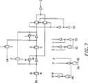
計算モジュール40のステージ2論理ブロック(STLB)の実施の形態を図6に示す。STLB444は、一般に、3つのマルチプレクサ660、680、及び696と、2つのビット記憶ユニット670及び688を含んでいる。第1のマルチプレクサ660の第1の入力はライン662上の信号DSを受け、第2の入力はライン694を介してビット記憶ユニット688の出力に結合されている。DSは、STLB444内への信号入力として働く。第1の、即ち上側の通路は、スイッチ663が閉じている時に、ライン694上の入力をライン664上のマルチプレクサ出力に結合する。スイッチ663は、ライン668上の信号Fによって制御される。第2の、即ち下側の通路は、スイッチ661が閉じている時に、ライン662上のDS信号をライン664上の出力に結合する。スイッチ661は、ライン666上の信号Mによって制御される。マルチプレクサ600、及びそれに類似の他のものを、以下に“デュアル制御マルチプレクサ”という。
【0039】
ビット記憶ユニット670は、入力としてライン664上のデュアル制御マルチプレクサ660からの出力を受けている。本発明の1実施の形態では、ビット記憶ユニット670は、図6に示すように1対の交差結合されたインバータ672及び674である。インバータ674は、一般に、インバータ690よりも弱く設計されており、マルチプレクサ660からのビット出力のどのような変化も、オーバドライブ用インバータ674によってビット記憶ユニット670内に配置できるようになっている。更に、インバータ674は、ライン666上の信号Mによって可能化されたり、不能化されたりする。従って、ビット記憶ユニット670は、計算モジュール440の若干の形態においては、簡単なインバータに見えるように構成することができる。
【0040】
デュアル制御マルチプレクサ680は、第1の入力として、ライン676上のビット記憶ユニット670の出力を受けている。マルチプレクサ680の他方の入力は、ライン678上の、STLB444への入力である信号DAに結合されている。マルチプレクサ660と同様に、マルチプレクサ680は2つの信号通路を有しており、各々はそれぞれのスイッチ681または683によって制御される。ライン682上の信号Sはスイッチ681を制御し、ライン684上の信号Lはスイッチ683を制御する。
【0041】
ビット記憶ユニット688は、入力としてライン686上のデュアル制御マルチプレクサ680の出力を受けている。ビット記憶ユニット670と同様に、1実施の形態におけるビット記憶ユニット688は、1対の交差結合されたインバータ690及び692からなり、インバータ692はインバータ672よりも弱く、そしてインバータ692はライン684上の信号Lによって選択的に可能化される。
【0042】
マルチプレクサ696は、第1の入力として、ライン694上のビット記憶ユニット688の出力を受けている。マルチプレクサ696への第2の入力は、ビット記憶ユニット670の出力676から受けている。マルチプレクサ696は更に選択入力SXをも有しており、マルチプレクサ696はライン697からそれを受け、この入力SXはマルチプレクサの入力の1つを選択させてライン698上に出力させる。
【0043】
ライン698はインバータ700に結合されており、インバータ700はバッファリングメカニズムとして働き、またライン702上に信号Qを出力する。
【0044】
更に、STLB444は、選択及び可能化ロジックを含んでおり、このロジックはマルチプレクサ660及び680内のいろいろなスイッチを選択し、またビット記憶ユニット670及び688内のインバータ674及び692をそれぞれ可能化する。1実施の形態における選択及び可能化ロジックは、NORゲート704、NANDゲート710、NANDゲート716、及びインバータ722及び724を含んでいる。
【0045】
NORゲート704は、ライン706上の第1の入力MCと、ライン668を介してNANDゲート710の出力から受ける第2の入力とを有している。NORゲート704は、ライン666上に信号Mを出力してスイッチ661を制御させ、インバータ674を可能化させる。
【0046】
NANDゲート710への入力は、ライン712上のEN及びライン714上のASであり、これらはSTLB444への入力である。NANDゲート710からの出力668は信号Fであり、これはマルチプレクサ660内のスイッチ663を制御する。
【0047】
NANDゲート716は、入力信号として、ライン718上の信号SCと、ライン720上の信号S2とを受けており、これらは共にSTLB444への入力である。NANDゲート716の出力はインバータ724に結合され、インバータ724はライン682上にマルチプレクサ680内のスイッチ681を制御する信号Sを出力する。
【0048】
インバータ722もライン720上の信号S2を受け、ライン684上に信号Lを出力する。この信号は、マルチプレクサ680のスイッチ683及びビット記憶ユニット688内のインバータ692を制御する。
【0049】
図6には、STLB444のための選択及び可能化ロジックが、NOR、NAND、及び反転ゲートとして示されているが、当分野に精通していれば、多くの他のゲート組合せが可能であることは理解されよう。更に、図6においては、図を明瞭にするために、選択及び可能化ロジックの完全な接続は示されていない。しかしながら、当分野に精通していれば、信号名及び/またはライン番号からこれらの接続は明白であろう。他の図面においても、明瞭化のために同じ技法を使用する。
【0050】
図7は、図6に示した機能モデルの1つの特定の実施の形態を示している。図6に示したマルチプレクサ/スイッチ機能を実現するために、伝送ゲートが使用されている。本発明の他の実施の形態においては、伝送ゲートの代替としてパスゲートも受入れることができる。当分野に精通していれば、図7と図6とを比較すれば明白であろうから図7の詳細に関する説明は省略する。論理ゲート及びインバータで示されているが、図7及び他の図面の論理ゲートはいろいろなトランジスタ構成で実現できることも当分野に精通していれば明白であろう。更に、図7及び他の図面において、インバータ及び/または論理ゲートを追加、削除、及び/または再配列しても等価回路がもたらされることも、当分野に精通していれば理解されよう。
【0051】
図6に示すようにSTLB444は極めて柔軟であり、本明細書が参照として採り入れている前記米国出願08/821,475に詳細開示されているように、その入力へ結合される信号を変化させることによって、組合せ、逐次、またはメモリ機能として動作するように構成することができる。例えば、STLB444は、図8に示すように出力が2入力NORゲートの一方の入力に結合されている2入力ANDゲートのような、組合せ機能を実現することができる。このようにするためには、信号Aを入力SXで受けるように結合する。信号Bを入力ENで受けるように結合し、信号Cを入力ASで受けるように結合し、一方DA、DS、MC、SC、及びS2は全て論理低信号に結合する。ライン702上の出力Qはこの機能の出力である。
【0052】
図6に示す回路は、逐次機能を実現するように構成することもできる。図9は、D入力732、クロック入力734、及びQ出力736を含むフリップフロップ730を示している。図10は、図9のフリップフロップをマスタラッチ740及びスレーブラッチ750に分割して示している。図10では、マスタラッチ740のQ出力は、ライン742によってスレーブラッチ750のD入力に結合されている。スレーブラッチ750は、Q出力736を発生する。図9及び10に示すフリップフロップを実現するためには、図6の回路の入力を以下の手法で構成する。フリップフロップへのデータ入力(D)は、入力DSに結合する。STLB444からの出力Qも、図9に示すフリップフロップのQ出力である。クロック信号は、入力MC及びSCへ印加される。更に、もし可能化、クリア、及び/またはプリセットを望むのであれば、可能化信号を入力ENへ印加し、クリア信号またはプリセット信号を入力AS及びS2へ印加する。DAは、クリア信号の場合には論理低に接続し、またはプリセット信号の場合には論理高に接続する。SXは、論理低に結合する。このようにすると、DSにおけるデータビット入力は、ビット記憶ユニット670及びビット記憶ユニット688を直列に通過し、この実施は図10に示すものと類似のマスタ・スレーブフリップフロップとして動作する。
【0053】
ビット記憶ユニット670及び688を、本発明の1つの実施の形態におけるように交差結合されたインバータで実現する場合には、インバータ672及び690はそれぞれ、インバータ692及び674よりも強くすべきである。このようにすると、マルチプレクサからビット記憶ユニットへの入力データが状態を変えると(例えば、0から1へ)、その入力データがインバータ674及び/またはインバータ692をオーバドライブする。スイッチ661が開くと(高クロック信号で)、ビット記憶ユニット670の交差結合されたインバータは妨害を受けることなく、記憶した最後のビットを保持し続ける。同様にして、スイッチ681が開くと、ビット記憶ユニット688の交差結合されたインバータは妨害を受けることなく、記憶した最後のビットを保持し続ける。
【0054】
ラッチは、フリップフロップと同じようにして実現することができるが、1つのビット記憶ユニットだけを使用すればよい。低で活動する(アクティブロー)ゲートのラッチを形成するためには、S2をラッチゲートとして働かせ、一方DAラインをラッチへのD入力として働かせ、Qをラッチ出力として働かせる。SC、MC、DS、及びSXは全て論理低に保持し、一方AS及びENは論理高に保持する。高で活動する(アクティブハイ)ゲートのラッチを形成するためには、SCをラッチゲートとして働かせ、DSをラッチへのD入力として働かせ、Qをラッチ出力として働かせる。S2、EN、及びASは論理高に保持し、一方MC、SX、及びDAは各々論理低に保持する。
【0055】
試験のために変更されたSTLB
前述したように、集積回路の試験についての伝統的な考え方によれば、ある回路を試験する際に良好な障害カバレッジを得る能力は、普通はその回路内に走査フリップフロップを挿入して被試験回路の状態をセット及び/または記憶させることを前提としている。図2を参照して説明したように、その設計内に既に存在しているフリップフロップの前にマルチプレクサを挿入しなければならないか、または図3を参照して説明したように、これらのフリップフロップをデュアルインタフェースデバイスに変換しなければならない。もし回路内に既に存在しているフリップフロップが、回路を完全に試験するためには不十分であれば、単に試験目的だけのために、付加的な回路(例えば、マルチプレクサ及び/またはフリップフロップ)を回路に追加しなければならない。従って、IC設計者がゲートアレイ内に若干の設計を実現することを望む場合には、ゲートアレイ内のある回路(例えば、機能モジュールまたはそれらの部分)を、試験の目的のために犠牲にしなければならない。
【0056】
図6の回路を試験するためには、伝統的な試験構造を使用する必要があろう。換言すれば、フリップフロップを実現しているアレイ410内の全てのSTLB444のためにマルチプレクサ・ベース走査を使用するためには、出力が関連するフリップフロップに結合されているマルチプレクサを実現するように、同一の、または他の機能ブロック420内の他のロジックを結合しなければならない(例えば、ステージ1ロジック442の1実施の形態内に含まれるマルチプレクサをこの目的のために使用することができる)。クロック・ベース走査を使用すると、より一層複雑になる。試験目的のための構造を実現するためにあるロジックを使用すると、典型的にはその同じ回路を他の目的のために使用する能力が排除されてしまう。
【0057】
それにも拘わらず、本発明による予め設計されたゲートアレイは、どの機能ブロック450の回路の全て、または一部も試験目的だけのために犠牲にすることを最小にし、そして前述したような従来のDFT規則に従ってユーザ設計回路を設計することを回避するような手法でそれを行う。更に、本発明による予め設計されたゲートアレイは、ゲートアレイによって最終的に実現されるユーザ設計回路内に逐次ロジックが配置されることには無関係に、ユーザ設計回路の試験を可能にする。
【0058】
本発明によれば、必ずしも通常動作において逐次機能を遂行するように最終的に構成されるとは限らないが、図6のSTLB444はビットを記憶する能力を含んでいるので、即ち、容易に逐次機能を遂行するように構成することができるから、アレイを試験できるようにする回路は各STLB444内に配置される。STLB444をカストマイズして(即ち、その入力へいろいろな信号を結合することによって)実現するユーザが限定した回路機能の基礎となる型(例えば、組合せ、逐次)には関係なく、試験目的のために各STLB444を実際に使用することができる。従って、本発明によるアレイによって実現される回路の試験は、回路の予備知識も、または設計者の係り合いも必要としない。
【0059】
図11は、本発明の1実施の形態における試験を可能にするように変更された図6を示している。図11に示すように、2つの付加的なデュアル制御マルチプレクサ802及び804が図6の回路に追加されている。デュアル制御マルチプレクサ660の出力はデュアル制御マルチプレクサ802の第1の入力に結合され、一方デュアル制御マルチプレクサ802の第2の入力はライン806上の試験データ(TD)を受けるように結合されている。デュアル制御マルチプレクサ802の出力は、ビット記憶ユニット670に結合されている。デュアル制御マルチプレクサ804の第1の入力は、デュアル制御マルチプレクサ680の出力に結合され、第2の入力はビット記憶ユニット670の出力に結合されている。デュアル制御マルチプレクサ804の出力は、ビット記憶ユニット688に結合されている。
【0060】
更に、図11においては、選択及び可能化ロジックは付加的にNORゲート814及びインバータ812を含んでいる。NORゲート814は、一方の入力に“列カット”(CC)信号を受け、第1の入力に“行カット”(CR)信号を受けている。以下に、CC及びCRをそれぞれ、列モード選択信号及び行モード選択信号ということがある。NORゲート814の出力は反転C信号を運び、一方インバータ812の出力は信号Cを運んでいる。信号C及び反転Cは、後述するように“凍結”指示信号として働く。反転Cは、マルチプレクサ802内のスイッチ816と、マルチプレクサ804内のスイッチ820とに結合されている。2つの付加的な信号、即ちTCLKLO及びTCLKHIが準備されている。TCLKLOはマルチプレクサ802内のスイッチ818に結合され、TCLKHIはマルチプレクサ804内のスイッチ822に結合されている。ビット記憶ユニット688からの出力であるTQは試験データ出力である。
【0061】
図から明らかなように、図11は試験回路の機能的動作を表しているに過ぎない。しかしながら、回路がトランジスタレベルで実現され、最適化されている時には、図11に示されている全ての論理素子の実際の分離した実現は必要ないかも知れない。例えば、図12は、図11に示すような試験回路を有するSTLB444の1つの特定実施の形態を示しており、図12の回路は最適化されている。図7と比較すれば理解できるように、各STLB444内に試験回路を実現するためには、図7の回路に極く僅かな変更を行う必要があるだけである。詳述すれば、図12には3つの付加的な伝送ゲート1002、1004、及び1006を付加して図11に示す機能を得ている。選択及び可能化ロジックに対しても若干の変更がなされている。当分野に精通していれば、図12と図11とを比較すれば明白であろうから、図12のさらなる詳細説明は省略する。当分野に精通していれば、論理ゲート及びインバータで示されてはいるが、図12及び他の図面の論理ゲートは、いろいろなトランジスタ構成で実現されることも明白であろう。更に、当分野に精通していれば、図12及び他の図面において、インバータ及び/または論理ゲートを追加、削除、及び/または再配列しても等価回路がもたらされることも理解されよう。
【0062】
再度図11を参照する。動作中、反転Cが論理高(Cが論理低)である場合には、マルチプレクサ802及び804内のスイッチ816及び820が選択されて回路は通常の態様で挙動し、それがユーザ設計回路によって決定されて遂行するように構成されているどのような組合せ、逐次、またはメモリ機能をも遂行する。反転Cが論理低信号(Cが論理高)である時には、STLB444は凍結動作モードにあって回路の状態を凍結させ(もしくは、捕獲し)、STLB内に記憶しているビットがユーザ設計回路入力に応答するのを阻止し、マスタ・スレーブフリップフロップとして挙動する。凍結動作モード(反転Cが論理低)にある時には、信号TCLKLO及びTCLKHIを通して分配される試験クロックTCLKが試験データを、ラインTD上のデータ入力からビット記憶ユニット670及び688を通してシフトさせ、TQを通して出力させる。本発明の1実施の形態では、TCLKLO及びTCLKHIは同一クロック信号から導出された互いに反転している信号であり(即ち、TCLKLOが高である時にはTCLKHIは低であり、逆もまた真である)、アレイが凍結されている時に限り両TCLKLO及びTCLKHIがTCLKを分配し、それ以外はスイッチ818及び822を開いたままにさせる。
【0063】
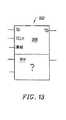
次に図13のデバイス902を参照する。STLB444は、クロック・ベース走査に使用されるデバイス304(図3)とやや似た挙動をする。図3のデバイスと同様に、図14のデバイスも2つのインタフェースの間でスイッチする。しかしながら、フリップフロップとして単に2つのインタフェース間でスイッチするのではなく、インタフェースがデバイス902へスイッチした時に、デバイス902の内部回路は、同一回路が使用されるのではあるが、再構成される。前述したように、STLB444の機能は、その入力を変えるだけで変化させることができる。従って、「凍結」が選択されている場合、通常動作モードにおいてユーザ設計機能(例えば、組合せ、逐次、またはメモリ)を実現するSTLB444内の回路(デバイス902の下側部分に“?”で表されている)は、マスタ・スレーブフリップフロップ(デバイス902の上側部分906内に表され、試験データイン(TD)、試験クロック(TCLK)(TCLKLO及びTCLKHIを導出するクロック)、及び試験データアウト(TQ)を有している)を実現するように再構成される。ラインC(図11)上に論理高信号を印加することによって「凍結」を選択すると、STLB444は正規STLB入力信号(例えばDS、DA)には応答しなくなり、試験クロック(TCLKLO及びTCLKHI)及び試験データ入力信号(TD)に応答する以外は、2つの内部ビット記憶ユニットは状態を変化させない。
【0064】
アドレス可能なモード制御
機能ブロック420のアレイ410においては、各計算モジュール440のSTLB444は、そのSTLB444のために適切な列及び行モード選択信号を選択することによって、通常動作モード、または凍結動作モードを選択することができる。換言すれば、アレイ410内において、STLB444はサブアレイを形成し、各STLB444は行及び列によってアドレス可能である。列信号(CC)及び行信号(CR)は一緒になって信号Cを作り、STLBが凍結動作モードにあるのか、通常動作モードにあるのかを決定する。もしそのモジュールの列及び行モード選択信号が共に論理低信号であればSTLBは通常動作モードで動作し、ユーザ設計回路によって遂行させるようにSTLB444が構成されているどの機能(例えば、組合せ、逐次、メモリ)をも遂行する。もし列または行モード選択信号の何れかが論理高であれば、STLBは凍結動作モードにある。従って、列及び行の両モード選択ラインを表明させなければ、何れか1つのSTLB444の挙動は、通常動作モードにおいて試験するように選択することができる。
【0065】
例えば、図14は、アレイ410のSTLBijによって形成されたサブアレイ1210の一部分を示しており(図14には、ステージ1論理ブロック442及び通信モジュール460は示されていない)、STLBはフリップフロップとして示されている(即ち、図13について言えば、各STLB毎の上側インタフェースが示されている)。NORゲート814及びインバータ812は、図14では単にORゲート814’として示されており、その一方の入力は列モード選択ライン1212iに結合され、第2の入力は行モード選択ライン1216jに結合されている。各列1モード選択ライン12121及び行1モード選択ライン12161上に論理低を印加し、各列0モード選択ライン12120及び行0モード選択ライン12160上に論理高値を印加することによって、STLB44411だけが通常動作モードで動作するように選択される。STLB44400、STLB44401、及びSTLB44410は凍結され、全てのSTLBが凍結されている間にシフトインされたデータを刺激データとして保持する。STLB44411は、例えばSTLB44400、STLB44401、及びSTLB44410から受けた刺激データの結果を計算し、ライン12121及び12161が表明されることによってそれが凍結されている時にその結果を捕捉する。以上のように、どのSTLBijも、通常動作モードにおける適切な動作について選択的にアドレスし、試験することができる。アレイ410によって実現されている回路の試験中に作動させるためにどのSTLBでも選択するこの能力を、本明細書では“アドレス可能なモード制御”呼んでいる。
【0066】
試験
アレイ410によって実現されている回路の状態を制御するために、刺激値をアレイ410内の全てのSTLBに印加する。そのようにするためには、STLBサブアレイ1210の各列1220i内のフリップフロップを“デイジーチェーン”化する。図14を参照する。列1 12201刺激値がSTLB44410内のフリップフロップ110110内への第1の入力である。フリップフロップ110110のQ出力はフリップフロップ110111のD入力に結合されている。デイジー・チェーンは列12201のボトムまで続いている。同様に、列0 12200内のSTLB(例えば、STLB44400及びSTLB44401)のフリップフロップは同じようにデイジーチェーン化されている。
【0067】
回路を既知の状態に置くために、先ず、全ての行凍結ライン1216j及び/または全ての列凍結ライン1212jに論理高値を印加することによって、全ての行及び列を凍結に選択する。刺激値をシフトレジスタ1502内に配置する。本発明の1実施の形態では、シフトレジスタ1502の各ステージ1504iの出力は、各列内の第1のフリップフロップ1101i0のTD入力に結合されている。試験クロック(TCLK)1534を印加して、試験刺激値を一時に1つ、シフトレジスタステージ1504iからそれぞれのデイジーチェーンに印加すると、それらはデイジーチェーンを介して各列1220iを通って同時にシフトする。次いで、選択されたSTLBijに対応する行及び列両凍結ラインに論理低値を配置することによって選択されたSTLB444ijが通常動作モードの動作ために選択される。
【0068】
同様に、被試験回路の結果を観測するために、フリップフロップのアレイ、特に通常動作モードのために選択されたばかりのSTLB内のそれらを、適切な行及び/または列モード選択ラインを介して凍結させ、再びTCLK1534を印加することによって、得られたデータをシフトアウトさせる。本発明の1実施の形態では、得られた値はシフトレジスタ1522内へシフトインされ、そこから、これらの値はICからシフトアウトされ、観測される。本発明の他の実施の形態は、全ての列を同時にではなく、データを一時に1列ずつシフトインまたはシフトアウトさせることができ、及び/またはシフトレジスタ1502、1512の使用を必要としないことができる。1実施の形態では、図示のようにシフトレジスタが含まれている場合に、これらのシフトレジスタは回路に対して直列及び並列の両試験データアクセスが可能である。
【0069】
区分試験
一般的に言えば、本発明による方法に従ってある回路を試験する場合、ユーザ設計回路内で互いに接続されているSTLB444は同時に試験すべきではない。前述したように、各STLBを通常動作モードで動作するように選択的にアドレスし、一方他のSTLBを同時に凍結動作モードのままとすることができる。更に、一時に1つのSTLBブロック444を試験するのは、特に単一のIC上に数千のSTLB444が存在している場合には、非効率的であり、時間を消費する。各STLBブロックを個々に試験することは、必然的に、全てのSTLBを繰り返し凍結し、試験刺激値をシフトインさせ、選択された1つのSTLBを作動させ(即ち、Cを表明させないことによって、選択されたSTLBを通常動作モードに配置し)、そして全ての結果値をSTLBからシフトアウトさせることを伴う。
【0070】
上述したシナリオを回避するために、本明細書において“区分試験”と称する本発明によるゲートアレイを試験する1つの方法では、可能な限り多くの“隣接”していないSTLB444を同時に試験するように回路を区分する。STLB444は、もし1つからの出力が他の状態に影響を与えれば“隣接”であるものと考える。例えば、もし(1)1つのSTLBのQ出力から第2のSTLBの何れかの入力(SXを除く、SXはビット記憶ユニット内に記憶されている値に何等の変化も生じさせないからである)まで直接的な接続ラインが存在するか、または(2)ステージ1ロジック442、インバータステージロジック464、ドライバステージロジック462からの組合せロジック、またはSTLBを通る組合せSX−Q通路が付加的に介在している(1)のような接続が存在すれば、2つのSTLBは“隣接”である。
【0071】
例として、図23は、実線によって示されているようにユーザ設計回路で接続されている6つのSTLB24441-6を示している。破線は、どのSTLBが“隣接”であるかを示している。STLB24441とSTLB24444とは、これら2つのSTLBの間には1つのインバータだけしか存在していないので隣接である。STLB24442とTLB24444及びSTLB24445とは、これらのSTLBの間にはそれぞれドライバロジック及び組合せロジックしか存在していないので隣接である。同様に、STLB24443はSTLB24445と隣接であり、STLB24444はSTLB24446に直接接続されており従って隣接である。最後に、STLB24445とSTLB24446とは、それがSTLB24444のSX入力を介して接続され、2つの間には1つの組合せロジックしか存在しないので隣接である。
【0072】
第1の区分は、図23のSTLB24441、24442、24443、及び24446のような隣接していないSTLB444の最大セットを含むように決定される。前述したように適切な刺激値をシフトインさせた後に、区分内の全てのSTLB444を作動させ(通常動作モードに置き)、一方アレイ内の残余のSTLB444は凍結のままとして刺激データを維持させる。第1の区分のSTLBが試験されてしまうと(作動させられ、得られた捕捉値のシフトアウトを含む)、24444及び24445のような次の区分が試験される。これらの分割は、当分野においては公知のグラフカラーリング技術によって決定される。
【0073】
区分試験に関して詳述すると、図15は、STLB444のサブアレイ1210のやや大きい部分を示しており、STLBは列モード選択ライン1212i及び行モード選択ライン1216jの各交差点に存在している。各STLBのためのロジックは、明瞭化のために示されていない。図中“X”で示されているSTLBは、これらのモジュールが試験プロセス中に互いに影響し合わないので(それらがユーザの設計(図示してない)では互いに“非隣接”であるから)第1の区分部分例であり、作動させられるSTLBである。図15に示す区分部分のSTLB444を試験するために、先ず、例えば全ての行モード選択ライン1216j及び/または全ての列モード選択ライン1212iに論理高を印加してアレイ1210内の全てのSTLB444を凍結させ、これらのSTLBをデイジーチェーン化されたフリップフロップとして機能させる。次に、TCLKを印加することによって、図14で説明したように列デイジーチェーンの態様で全てのSTLB内に刺激データをシフトインさせる(以下、“シフト動作”という)。本発明の1実施の形態によれば、シフト動作はSTLBが凍結された後に限って行うことができる。
【0074】
シフト動作が完了すると、区分マスクが印加される。区分マスクは、選択された(“X”でマークされている)STLBだけを通常に作動させ、他のSTLBは凍結させたままとして刺激値を送り出させる。このようにするためにモード選択値を列モード選択ライン1212jに印加すると、STLBが作動している第1の行内の列上にのみ論理低値が現れるようになる。モード選択値は、行モード選択ライン1216jにも印加されるので、1つの行だけが、即ち第1の行が論理低値を有するようになる。即ち、図15の例では、行0が最初に試験される。列4の行0内のSTLBだけを作動させるために、列7:0に印加される値は11101111であり、行7:0に印加される値は11111110である。行0内の選択されたSTLBが作動し終わると、行1内の選択されたSTLBが同じようにして、例えば列7:0に10111110のマスクを印加し、行7:0に11111101のマスクを印加することによって作動させられる。一時に1つの行だけを作動させるように選択されているが、本発明のさまざまな実施の形態では2以上の列を選択することができることに注目されたい。当分野に精通していれば理解されるように、本発明の他の実施の形態は、一時に2以上の行を選択できるが、一時に1つの列だけを選択するようになっている。全ての行内の全ての選択されたSTLBが作動し終わるまで、各行のためにこのサイクルが繰り返される。全ての行内の全てのSTLBがその分割のために作動し終わると、全てのSTLBは再度凍結される。次いで、TCLKを印加することによってシフト動作が遂行され、列デイジーチェーン態様で捕捉されたデータが観測のためにシフトアウトされる。次に新しい区分が選択され、手順(即ち、刺激データのシフトイン、選択されたSTLBの行毎の作動、及び捕捉されたデータのシフトアウト)が繰り返される。幾つかの区分が必要であろうから、各STLBは少なくとも1回は作動させられる。本発明の発明者らは、本発明によって設計された約40,000の機能ブロックを有するゲートアレイの場合、アレイ410を完全に試験するためには約1ダースの区分が必要であることを見出した。
【0075】
走査エミュレーション試験
図14に基づいて説明した本発明の実施の形態を使用すると、伝統的な走査試験をエミュレートするためにもSTLBのアレイを使用することができる(以下に“走査エミュレーション試験”という)。このようにするために、区分試験について上述したように、先ず刺激データが全てのSTLB内にシフトインされる。即ち、全ての列モード選択ライン及び/または全ての行モード選択ラインに1を印加することによって全てのSTLBを凍結させ、次いでTCLKを印加してデータをシフトインさせる。次に、区分を選択するのではなく、全てのSTLBが同時に作動させられる。即ち、全ての列モード選択ライン及び全ての行モード選択ラインを0にセットする。従って、走査エミュレーション試験においては、全てのSTLBは刺激データを受入れるために(または、得られたデータをシフトアウトさせるために)凍結されるか、または全てのSTLBは通常動作モードにあるかの何れかである。
【0076】
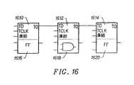
このようにすると、回路内に使用されている全てのフリップフロップは、将に伝統的な走査技術のように試験のために使用される。本発明によるシステムを走査エミュレーション試験のために使用する場合、それはユーザにはクロック・ベース走査にやや似て見える。しかしながら、ユーザ設計回路に従って、例えば組合せ機能のような逐次機能以外の何かを通常動作モードで実現するようにSTLBを構成する場合、通常動作モードにおいてSTLBが実現する機能には無関係に全てのSTLBは凍結されたフリップフロップとして動作するから、データをシフトイン及びシフトアウトさせる際に伝統的な走査のために予期されるビットに加えて特別ビットが発生する。一方、本発明による走査エミュレーション試験中には凍結される。図16を参照する。デイジーチェーン化された試験フリップフロップ1610、1612、及び1614は、通常動作モードにおいてはフリップフロップ1616、ANDゲート1618、及びフリップフロップ1620として動作するSTLB内にあることができる。伝統的な走査においては、試験機はANDゲート1618(組合せロジック)を含むSTLB内に1つのビットを配置できることを予期していない。一旦認識されると、走査技術に従って評価を可能にするために、特別ビットを試験ベクトル内に挿入することができる、及び/または結果内に現れる特別ビットを無視することができる。
【0077】
強化されたシフト動作
当分野に精通していれば理解されるように、走査技術を含む従来の技術においては、ユーザの設計内のフリップフロップを、付加的なクロック舵取り回路を追加しなければ容易に試験できないことが多い。それは、フリップフロップがエッジでトリガされるデバイスであるにも拘わらず、試験刺激データは静的パターン以外では生成することができないからである。例えば、再度図10を参照し、マスタラッチ740は、クロック入力734が低である間にそのD入力732に到来するデータをロードする(そのデータに対して透明である)。クロック信号の立上がりエッジの後に、データは、クロック信号が高である時にロードするスレーブラッチ750内に捕捉される。フリップフロップはクロックエッジにのみ応答するから、付加的な試験構造を用いなければ、伝統的な技術ではフリップフロップ730の内部動作を容易に試験することはできない。例えば、クロック信号が静的な論理低である場合、D入力732上のどの値もマスタラッチ740へロードされるが、スレーブラッチ750には何もロードされない。伝統的な走査技術においてはスレーブラッチ750のQ出力736だけが観測可能であるから、マスタラッチ740に対してだけの変化の効果は観測することができない。クロック信号が静的な論理高である場合、マスタラッチ740はロードせず、スレーブラッチ750だけがマスタラッチ740の出力をロードする。不幸にも、試験データのシフティングは、既にマスタからスレーブへロードされているから、スレーブロードは観測できる結果を有していない。従って、伝統的な技術では、回路の外側からクロックエッジ遷移を導入するために、クロック信号の十分な外部制御可能性を維持するように注意を払わない限り、各フリップフロップ内部の故障として現れる欠陥は容易に分離されない。
【0078】
それにも拘わらず、本発明による単一のTCLKによってクロックされるシステムを使用すると、マスタ及びスレーブラッチは各々、シフト動作中に独立値を含むことができる。換言すれば、フリップフロップラッチは完全に制御することができ、クロックエッジを必要とせずに論理低及び論理高レベルだけを使用して観測することができる。更に、STLBが通常動作モード中にメモリ機能を遂行するように構成されている場合には、2つのラッチは独立メモリビットを記憶し、従って試験中、それらを独立的に制御し、観測することが望ましい。
【0079】
図17は、フリップフロップ1101のマスタラッチ1102及びスレーブラッチ1104を示すために、再び図示されている図14のSTLB444ijの使用を示している。マスタラッチ1102は一般にビット記憶ユニット670(図11)で識別することができ、スレーブラッチ1104は一般にビット記憶ユニット688(図11)で識別することができる。
【0080】
独立値を各マスタ及びスレーブラッチ内へシフトさせるために、本発明によるシステムは、TCLKを各マスタ及びスレーブラッチへ別々にゲートする。TCLKLO及びTCLKHIは、ゲートされたTCLKから導出される信号である。詳細について図18を参照して以下に説明する。
【0081】
図18は、本発明のシステムのより詳細なブロック図である。図14に示すものと同様に、図18に示されているSTLB(444ij)の2×2アレイは、各フリップフロップのマスタ及びスレーブラッチを示している。フリップフロップ従ってラッチは、図14で説明したようにデイジーチェーン化されている。各STLB444ijは、関連する行モード選択ライン1216j及び列モード選択ライン1212iに結合されているORゲート814’ijを有している。各関連ORゲート814’ijの出力“C”は、それぞれのSTLBの各マスタラッチ1102ij及びスレーブラッチ1104ijの凍結入力に結合されている。
【0082】
更に、いろいろな試験支援ロジックが示されている。このようなロジックは、本発明の1実施の形態では、ASIC400(図4)の周辺領域430内に現れている。試験支援ロジックは、シフトレジスタ1502、シフトレジスタ1512、シフトレジスタ1522、及び試験コントローラ1570を含む。
【0083】
シフトレジスタ1502は、フリップフロップ1504iからなる。シフトレジスタの各ステージ、即ち各フリップフロップ1504iは、関連する列の第1行(行0)内のそれぞれのマスタラッチ1102ijのデータ入力に結合されている。例えば、フリップフロップ15040はマスタラッチ110200のTD入力に結合されている。同様に、フリップフロップ15041はマスタラッチ110210の試験データ入力に結合されている。
【0084】
シフトレジスタ1502内の各フリップフロップ1504iは、ORゲート1506iの入力にも結合されている。各ORゲート1506iの第2の入力は、CC1に結合されている。各ORゲート1506iの出力は、ANDゲート1508iの第1の入力に結合されている。各ANDゲート1508iの第2の入力は、CC0ラインに結合されている。各ANDゲート1508iの出力が、列モード選択信号(CC)1212iである。
【0085】
フリップフロップ1524iを含むシフトレジスタ1522も含まれている。各フリップフロップ1524iは、各列の最後の行内のスレーブラッチ1104ijのTQ出力を受けるように結合されている。
【0086】
行の試験支援ロジックも、列のための設けられているものと類似のシフトレジスタ及び組合せロジックを含んでいる。詳しく述べれば、シフトレジスタ1512は、マスタ・スレーブフリップフロップ1514jからなる。シフトレジスタの各ステージ、即ち各フリップフロップ1514jは、ORゲート1516jの入力に結合されている。ORゲート1516jの第2の入力は、CR1 1546に結合されている。各ORゲート1516jの出力は、ANDゲート1518jの第1の入力に結合されている。各ANDゲート1518jの第2の入力は、CR0 1544に結合されている。各ANDゲート1518jの出力が、行モード選択信号(CR)1216jである。
【0087】
クロック制御ロジックも設けられている。クロック制御ロジックは、各行毎にANDゲート1526j、ANDゲート1528j、及びインバータ1530jを含んでいる。各ANDゲート1526jの第1の入力はシフト信号ライン1532に結合され、第2の入力はインバータ1530jに結合されている。インバータ1530jの入力は、TCLK信号ライン1534に結合されている。各ANDゲート1526jの出力はTCLKLOを発生し、関連する行内の各マスタラッチ1102ijのG入力に印加する。各ANDゲート1528jは遅延シフト信号ライン1533に結合されている。各ANDゲート1528jの第2の入力は、TCLK信号ライン1534に直接結合されている。ANDゲート1528jの出力はTCLKHIを発生し、関連する行内の各スレーブラッチ1104ijに印加する。
【0088】
ライン1533上に遅延シフト信号を得るために、シフト1532がラッチ1535のD入力に結合され、一方ラッチ1535のゲートはTCLKに結合されている。ラッチ1535のQ出力が遅延シフト信号ライン1533に結合されている。1実施の形態においては、このラッチ1535は、図18内の全ての試験信号(例えば、CC0、CC1、CR0、CR1、TCLK、シフト、及び遅延シフト)を制御する試験コントローラ1570の部分である。
【0089】
各ANDゲート1526j、1528jは、可能化入力をも含んでいる(実際には、3入力ANDゲートの第3入力であることができる)。各ANDゲート1526jへの可能化入力は、各スレーブラッチ1538jのQ出力(即ち、各フリップフロップ1514jのQ出力)に結合されている。各ANDゲート1528jへの可能化入力は、各マスタラッチ1536jのQ出力に結合されている。
【0090】
クロック制御ロジックを使用することにより、信号値がマスタ・スレーブフリップフロップによって捕捉される伝統的な試験方法とは異なり、独立値を各マスタラッチ1102ij及びスレーブラッチ1104ijへシフトイン、及びそれからシフトアウトさせることができ、それによって“強化されたシフト動作”で動作させることができる。例えば、試験刺激値を各列内へシフトインさせる時に、それぞれの試験データを供給するためにシフトレジスタ1502が使用される。データが列を通って適切なラッチ内へシフトインしてしまうと、その行のラッチへのクロックがターンオフされる。例えば、適切なデータ値が選択されたスレーブラッチ1104ijに到達するまで、データ値をラッチ内へシフトインさせることができる。次いで、そのスレーブへのTCLKHIがターンオフされる。ラッチを通る次のシフト時に、独立データ値を同じSTLBのマスタラッチ内へシフトインさせることができる。次に、マスタラッチへのTCLKLOをターンオフさせることができる。TCLKLO及びTCLKHIがターンオフされていないその列内の他のラッチは、シフトを続行する。このようにして、アレイ内の全てのSTLBの各マスタ及びスレーブラッチ内に独立値を配置することができる。
【0091】
より詳しく述べれば、そして例として図18においては、シフト動作中、TCLKでもクロックされているシフトレジスタ1512は、先ず全てが論理高値でロードされ、アレイ内の全てのTCLKLO及びTCLKHI信号へTCLKを分配できるようにされる。スレーブラッチ110401のための所望値が列0を通ってシフトし、それがスレーブラッチ110401内へシフトインしてしまうと、論理低値をマスタラッチ153601内へシフトインさせることによって、行1のためのTCLKHI15421がターンオフされ、ANDゲート15281を不能化させる。列0を通る刺激値の次のシフト時に、独立値がマスタラッチ110201内へシフトインされ、スレーブラッチ153801は論理低を受けてANDゲート15261を不能化させ、それによって行1内のマスタラッチ1104i1へのTCLKLO15401をターンオフさせる。論理低値はシフトレジスタ1512のマスタ及びスレーブラッチを通って前進的にシフトし、各マスタ及びスレーブラッチ1102、1104への全ての信号1540j及び1542jがターンオフされてしまうまで、各行のためのTCLKLO及びTCLKHI信号を1つずつ不能化して行く。
【0092】
マスタ及びスレーブのラッチ1102ij、1104ijの両方の中のデータを独立的に観測するために、アレイからデータをシフトアウトさせるための類似メカニズムが使用されている。先ず、シフトレジスタ1512に論理低値がロードされ、全ての行内のTCLKLO及びTCLKHIへのTCLKの分配が阻止される。次いで、論理高値がシフトレジスタ1512内へ前進的にロードされる。例えば、最初の論理高値がマスタラッチ15361内にロードされ、ANDゲート15281を可能化し、行1内のTCLKHIをターンオフさせる。行1内のスレーブラッチ1104i1内に記憶されているデータはレジスタ1522へシフトアウトする。次いで、論理高値はスレーブラッチ15381に受けられ、ANDゲート15261を、従って行1内のTCLKLOを可能化する。行1内のマスタラッチラッチ1102i1に記憶されているデータはシフトアウトし(行1スレーブラッチを介して)、シフトレジスタ1522によって受けられる。各TCLKHI及びTCLKLOが順次に可能化される。それらの全てが可能化された時点には、データの半分がアレイからシフトアウトしている。残余の半分のデータは、全てが可能化されると、即ちTCLKが各行上にゲートされるとシフトアウトする。
【0093】
図18において、CR0 1544、CR1 1546、CC0 1548、及びCC1 1550は、アレイの動作モードを決定するモードラインである。例えば、全てのモードラインが論理低である場合には、回路は通常動作モードで(STLBが凍結されずに)動作する。もしCC0及びCC1が共に論理高であれば(及び/または、もしCR0及びCR1が共に論理高であれば)、アレイは凍結動作モードになり、TCLKの表明によって、シフト動作または強化されたシフト動作を遂行し、試験刺激値をアレイ内へシフトインさせたり、またはアレイからシフトアウトさせることができる。もしCC0が論理高であり、CC1が論理低であり、CR0が論理高であり、そしてCR1が論理低であれば、STLBはアドレス可能なモード制御のために可能化され、シフトレジスタ1502及び1512内へシフトインされた値は、どのSTLBを凍結動作モードにし、どれを通常動作モードで動作させるかを制御する。
【0094】
シフトレジスタ1502及び1512が複数の目的に役立っていることに注目されたい。シフトレジスタ1502は、シフト動作中には刺激値をシフトインさせるために使用されるが、一旦刺激値がSTLB内へシフトインされると、そのシフトレジスタを他の目的、例えばアドレス可能なモード制御のために使用することができる。同様に、シフトレジスタ1512は、シフト動作中にはクロック制御のために使用されるが、シフト動作が完了した後は、そのシフトレジスタ1512もアドレス可能なモード制御のために使用することができる。
【0095】
図5を参照して説明したように、他のロジックは、アレイ410から形成された何等かの回路の一部であることができる。例えば、いろいろな組合せ回路(例えば、ステージ1論理ブロックまたはインバータステージ464)は、何れかのSTLB444の間に位置することができる。それにも拘わらず、発明者らは、本発明による回路を使用し、設計する場合に、典型的には3−4非STLBステージだけが互いにリンクされ、使用される全てのロジックの1/4乃至1/3は本発明による機能ブロック420のSTLB内へマップされることを見出した。従って、試験回路を実現し、ゲートアレイを試験するために本発明によるシステムを使用すると、ユーザ設計を変更することなく、良好な障害カバレッジが容易に達成される。
【0096】
当分野に精通していれば理解されるように、アレイは機能ブロック420によって形成されているが、アレイはSTLBによっても形成される。本明細書に使用している“サブアレイ”という用語は説明を明瞭にするためだけに使用されているものであって、本発明を限定することを意図するものではない。また、本発明の実施の形態によるアレイは、STLBに関して説明した原理に従って、及びステージ1ロジック、インバータステージ、またはドライバステージのような他の散在するロジックなしに、完全に論理ブロックで形成することができることも理解されたい。
【0097】
トライステート競合予防
とは言え、もしドライバステージ462が含まれていれば、本発明によるシステムの実施の形態は、シフト動作中に、これらのドライバステージ462によって駆動される信号が互いに争うことも防ぐ。図19は、通信モジュール460のドライバステージ462の実施の形態を示している。トライステートバッファ1602は、第1の入力として信号DIを受け、信号Zを発生する。トライステートバッファ1602は更に、その可能化入力に信号EIをも受けている。
【0098】
図20は、図19に示したドライバステージ462の実施の形態の特定例をより詳細に示す図である。トライステートバッファ1602は、pチャネルトランジスタ704、nチャネルトランジスタ1706、NANDゲート1708、NORゲート1710、及びインバータ1712及び1714で実現されている。信号EIはインバータ1714へ入力される。インバータ1714の出力は、NANDゲート1708の一方の入力と、インバータ1712とに結合されている。インバータ1712の出力は、NORゲート1710の一方の入力に結合されている。入力信号DIは、NANDゲート1708の第2の入力と、NORゲート1710の第2の入力とに結合されている。NORゲート1710の出力は、トランジスタ1706のゲートに結合されている。トランジスタ1704のドレインはトランジスタ1706のドレインに結合されていて、出力Zを形成している。
【0099】
図21は、図19に示したような2つのトライステートドライバ1602A及び1602Bを示しており、ドライバの出力はライン1802上で互いに結合されており、各トライステートドライバは各々、STLBが凍結された時には、その入力が関連するフリップフロップ1801jに(即ち、STLBから)結合される入力を有している。図面を明瞭にするために図示してないが、STLBが凍結された時には、フリップフロップ1801jはデイジーチェーン態様に結合される(通常動作モードでは、及び以上に詳細に説明したように、それぞれのSTLBは逐次機能以外の機能を遂行することができる)。トライステートドライバ1602Bの、ライン1802上に論理低値を送り出す能力を試験したいものとする。そのようにするために、フリップフロップ18011-4内に示されているパターン(X100)(但し、Xは“ドントケア”値である)をフリップフロップ内へシフトインさせる必要がある。値A(論理高または論理低の何れか)が、その列内の次のフリップフロップであるフリップフロップ18015内へシフトインされる。しかしながら、最終クロックシフトの直前のクロックシフト(上述したパターンでシフトさせる)では、フリップフロップはパターン100Aを保持しており、もしA≠1であれば、両トライステートドライバ1602A及び1602Bは可能化され、それらがライン1802上で争い合うことになる(これはその時点で、真の50%である)。
【0100】
本発明の実施の形態によれば、シフト動作中の競合を予防するために、全てのトライステート出力は論理高値に保持される。図22は、図20の回路に追加された付加的な入力である反転THを示している。インバータ1712(図20)はNANDゲート1712’に置換され、一方の入力に反転THを受け、第2の入力としてい1714からの出力を受けている。付加的なpチャネルトランジスタ1804が、トランジスタ1704と並列に結合されている。トランジスタ1804のゲートも入力の反転THに結合されている。反転THが論理高である時には、回路は図20におけるように機能する。反転THが論理低にされると、論理高(VDD)信号がZ上に駆動される。シフト動作に入った時に、反転THを全てのトライステートドライバに結合し、反転THを論理低にすることによって、シフト動作中のトライステート出力上の競合は阻止される。
【0101】
以上に、ASICを試験するために使用される伝統的な技術に優る幾つかの長所を有する本発明によるシステムを説明した。第1に、各STLB内の試験回路が各機能ブロック内に予め設計されており、従って、ゲートアレイによって実現されている究極的なユーザ設計回路に依存もしないし、また設計者は彼自身で試験回路を挿入する必要もない。
【0102】
特定の機能ブロックのロジックも、試験だけに専用である必要はなく、試験及び通常の両動作機能を遂行するために使用することができる。換言すれば、STLB回路は、凍結及び通常動作モードのために再使用される。STLBは、ユーザ設計回路内で逐次ロジックを実現するためには必要としなくても、各STLB内のデータを制御及び観測できる。即ち、試験目的のために特別フリップフロップを挿入しなくても、組合せロジックさえも試験可能である。更に、本発明による試験を実現するためには、最小の付加的なトランジスタを機能ブロック420に付加するだけでよい。
【0103】
更に、各STLBにはアドレス可能なモード制御が設けられており、各機能ブロック内の各STLBを個々に作動させることができる。それにも拘わらず、ゲートアレイによって実現された全回路を、区分試験の動的な区分けを使用して比較的迅速に試験することができる。
【0104】
本発明により設計されたゲートアレイは伝統的な走査技術をエミュレートすることもでき、回路設計者は伝統的な走査試験の気楽さで、ゲートアレイをその手法で試験することができる。
【0105】
最後に、試験クロック信号は、試験目的のために使用されるフリップフロップを形成している各マスタ及びスレーブラッチを独立的に可能化、及び不能化することができ、試験フリップフロップのマスタ及びスレーブラッチ内へデータを独立的にシフトインさせたり、それらからシフトアウトさせたりすることを可能にしている。本発明に従ってラッチ及びTCLKを使用することによって、試験用エッジトリガフリップフロップに伴う諸問題が排除されるから(全ての試験は静的なパターンで容易に実施される)、IC設計に普通に使用される殆どのDFT規則も排除される。
【0106】
この説明に見出しを使用したが、これらは読者を案内するのに役立たせるだけに過ぎず、本発明を限定する意図はない。
【0107】
以上に説明した特定の実施の形態は、単に本発明の原理を例示したに過ぎず、当業者ならば本発明の範囲及び思想から逸脱することなく、さまざまな変更をなすことができよう。従って、本発明の範囲は特許請求の範囲によってのみ限定されるものである。
【図面の簡単な説明】
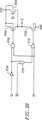
【図1】 複数のフリップフロップを含む回路の一般化した機能ブロック図である。
【図1a】 図1の図であって、一般的に走査技術を示している。
【図2】 マルチプレクサ・ベース走査が使用される場合の図1のより詳細な表現である。
【図3】 クロック・ベース走査に使用されるデバイスの機能ブロック図である。
【図4】 本発明の1実施の形態によるASICの一般化したブロック図である。
【図5】 本発明の1実施の形態による機能ブロック420の一般化したブロック図である。
【図6】 試験を実施する回路は示されていない、本発明の1実施の形態によるステージ2論理ブロック444の機能ブロック図である。
【図7】 図6の回路図である。
【図8】 図6に示す回路によって実現することができる組合せロジックの機能ブロック図である。
【図9】 D型フリップフロップの機能ブロック図である。
【図10】 マスタラッチ及びスレーブラッチを含む図9のD型フリップフロップのより詳細な機能ブロック図である。
【図11】 本発明による試験を可能にする回路を更に含む図6の機能ブロック図である。
【図12】 図11の回路図である。
【図13】 図11の回路のより一般化した機能ブロック図である。
【図14】 本発明によるアレイの機能ブロック図である。
【図15】 区分試験に使用される時の本発明によるアレイのブロック図である。
【図16】 走査エミュレーション試験中に、本発明によるアレイを使用する場合、伝統的な走査技術には存在しない特別なデータのビットが存在し得ることを示すブロック図である。
【図17】 マスタ及びスレーブラッチに分割されたSTLBのブロック図である。
【図18】 試験支援回路を含む本発明によるアレイの機能ブロック図である。
【図19】 本発明によるトライステートドライバステージ462の機能ブロック図である。
【図20】 図19に示す回路の回路図である。
【図21】 シフトモード中のトライステートドライバ出力上の潜在的な競合を示すブロック図である。
【図22】 シフト中のトライステート競合を予防するために付加された付加回路を有する図20に示す回路である。
【図23】 “隣接”及び“非隣接”STLBを示すブロック図である。[0001]
(Field of Invention)
The present invention relates generally to dedicated integrated circuits (ASICs) and, more particularly, the invention relates to test gate arrays.
[0002]
(Background of the Invention)
In the semiconductor industry, the use of ASICs is expanding because a given circuit design engineer can achieve a relatively large amount of circuit functions in a relatively small package. Specifically, an ASIC is a customizable integrated circuit that has been customized to implement a circuit specified by a design engineer (“user design circuit”). One type of ASIC is a gate array, which typically includes an array of functional blocks, with each functional block including a specific number, arrangement, and type of semiconductor devices, such as transistors. Pre-designed and / or pre-assembled. Various connections are made between semiconductor devices in functional blocks and / or various connections are made between functional blocks to customize the gate array to achieve a specific user design circuit specified by the design engineer. (Ie, routing is customized).
[0003]
An ASIC that includes a gate array that is customized to implement a user-designed circuit must be tested to ensure that the user-designed circuit operates properly. The test must be able to detect faults that result in improper or unexpected circuit behavior as a result of defects (eg, physical problems with the circuit such as short circuits and / or improper circuit design). I must.
[0004]
Faults include stuck-at faults (SAF), delay faults, and current faults. SAF occurs when a particular connection in a circuit remains at (or “sticks to”) a logic low level or a logic high level no matter what signal is applied to the circuit. (Hereinafter, “logic low” means a “0” signal and is often a ground signal. “Logic high” means a “1” signal and VDDOften a signal. ) Delay faults occur when a circuit is designed to fit a specific propagation time, but actually operates much slower than expected. For example, even if the circuit is designed with confidence that the signal propagation time between the first point and the second point is 5 ns, the actual signal operation will change from the first point to the second point. If it takes 15 ns to reach the point, the circuit cannot operate properly. A current failure often occurs when a current is actually passed in a circuit using a CMOS device that does not pass a current when inactive. Defects that lead to current failures are often detected by testing for SAF.
[0005]
If integrated circuit testing is well designed, it is generally the gate level (ie, conceptual circuit design level including Boolean logic, flip-flops, etc.) by testing all connections between logic elements. Most SAFs could be detected at. In order to test all connections between logic elements, the test must be able to (1) control or set the value at a particular connection and (2) observe the value at a particular connection. For example, in order to test the connection between point A and point B for a stuck-at zero fault, the tester must be able to apply stimulus data to place a logic high on the connection line, and the tester must It is necessary to be able to observe the connection to see if and how the value has changed as a result of the stimulus data.
[0006]
In discrete circuit designs, the ability to control and observe a particular circuit is often done by simply probing the various connections between the logic elements of the circuit. However, in integrated circuits, it is generally not possible to probe the internal connections of the circuit, so that other test methods have to be developed.
[0007]
One integrated circuit test method that has gained popularity among IC designers is the “scan” test described below with reference to the block diagrams of FIGS. 1 and 1a. In FIG. 1,
[0008]
By taking advantage of the nature of the state machine of the circuit, the state of the
[0009]
Specifically, one of two techniques is typically used to implement a scan-type test: multiplexer-based scanning or clock-based scanning. “Multiplexer-based scanning” is a more widely used technique and will be described below with reference to the block diagram of FIG. The clock-based scanning will be described with reference to FIG.
[0010]
As shown in FIG. 2, each flip-
[0011]
In order to test
[0012]
Although the above test method has been described as useful for detecting SAF, multiplexer based scanning can also be used for testing for delay faults. In order to do so, the test data is transferred to the flip-
[0013]
If multiplexer-based scanning techniques are used, flip-flops already in the user's circuit design are used for testing, but each flip-flop in
[0014]
In addition, as a direct result of multiplexer-based scanning, a number of "testability design" rules that have become widely known and used in user-designed circuits to avoid problems during testing (DFT rule) exists. These DFT rules include:
* The circuit preferably has a flip-flop triggered on the falling edge.
Should not be designed to include. Otherwise, some flip-flops
The flop is clocked by the rising edge of the circuit clock, with some falling edges.
Clocked in In this situation, the test data
During flip-in, some flip-flops may not receive proper stimulus values.
There is a special test flip in the daisy chain to avoid this situation.
A flop must be included.
* Make sure that the clock is coupled to the clock pin only and flip-flops.
The gate that is coupled to the D input of the
Should be designed not to be coupled to the Otherwise, the test
Setup and hold time violations can occur during mode, and the circuit
The response value is not captured reliably.
* The Q output of a flip-flop is directly connected to the clock input of another flip-flop.
Both directly and indirectly (eg, through combinatorial logic or drivers)
Should not be combined (like a Johnson counter). Because
This is because the lock input is not fully controllable during the test. In other words,
The clock input of the entire circuit must be controllable to test the circuit
Absent.
* All gates through which the clock passes are also controlled during the test to shift the test value
Allows the clock to pass through without being affected by other values during
We must be able to For example, if the clock signal is 2-input AND
Applied to the first input of the gate, the output of the AND gate is flip-flop
The second input to that AND gate.
The force must be held at a logic high during the test value shift.
* All asynchronous clear and reset pins will interfere with shift mode
Must be gated so that it can be prevented.
Other DFT rules are also well known. Many of these DFT rules allow tests to be controlled and observed, for example, only with static patterns (logic high and logic low values) (ie no clock edge transitions can be generated). ) Is a direct result of the fact.
[0015]
As described above, multiplexer-based scanning is often developed not only by adding additional circuits (eg, multiplexers and additional flip-flops) to the circuit, but also by limiting the multiplexer-based scanning. DFT rules place considerable limitations on circuit design, but these are all only to allow circuit testing.
[0016]
A second type of scanning technique is “clock-based scanning” which will be described below with reference to FIG. Rather than replacing each flip-flop in
[0017]
The signal input to shift 314 indicates whether the upper interface should be activated or the lower interface should be activated. When the signal coupled to shift
[0018]
Clock-based scanning is advantageous over multiplexer-based scanning because the associated DFT rules are fewer for clock-based scanning than for multiplexer-based scanning. Because separate interfaces and test clocks are used for testing, it is not necessary to follow most clock related DFT rules when designing the underlying circuit. Nevertheless, clock-based scanning tends to be more expensive than multiplexer-based scanning, causing it to be less frequently used than multiplexer-based scanning. Furthermore, even with clock-based scanning, it is necessary to add flip-flops in the user-designed circuit where there are insufficient flip-flops present in the user-designed circuit for testing purposes.
[0019]
As described above, scanning techniques are widely used to test integrated circuits, but they have many limitations. Not only does scanning technology add a significant number of devices (eg, multiplexers and / or flip-flops) to the circuit design and occupies considerable real space, but using such additional circuitry is normal It will limit the availability of dredge circuits that can be used for circuit operation. In other words, in the gate array, by inserting multiplexers and / or flip-flops in the circuit for testing purposes, various functional blocks, or parts thereof, are sacrificed for testing purposes, and the normal (non- Can not be used to realize the logic used in the (test) part. In addition, when using scanning techniques, and especially multiplexer-based scanning, circuit design flexibility is limited because of the need to follow many DFT rules to allow circuit testing, or clock-based Scanning requires significant additional costs to include a suitable dual interface device.
[0020]
The inability to insert test circuits into the circuit until the circuit design is substantially complete makes the design of integrated circuits even more difficult. More specifically, knowledge of where a circuit's flip-flops and / or latches are located in the circuit and how they are connected is necessary for the ability to insert additional appropriate test circuits. Critical. Typically, a circuit is designed once and then the design is modified for testing purposes, replacing the flip-flops in the circuit with multiplexer / flip-flop combinations, or dual interface flip-flops. The circuit must then be further analyzed to determine whether additional flip-flops or clock steering logic needs to be inserted into the portion of the circuit to fully test the circuit. As described above, the test circuit can be added to the completed circuit design only with some prior knowledge of the IC designer. If there is space on the IC, it may not be necessary to redesign the user's circuit to accept the test structure.
[0021]
Also, due to the nature of scanning, it is necessary to operate all circuits simultaneously after placing stimulus data in each flip-flop. Therefore, when designing test vectors, it is important to ensure that appropriate stimulus values are placed in the circuit and to take into account all parts of the circuit that can affect the obtained capture values. You have to make an effort to calculate. Furthermore, since the source of the problem may not be immediately apparent, it becomes even more difficult to isolate faults when all circuits are operated simultaneously.
[0022]
Therefore, the circuit test realized by the gate array can be implemented inexpensively (represented in real space and other resources) without requiring prior knowledge of the circuit, and the circuit can be completely implemented without using complicated DFT rules. A gate array design that allows testing and can be operated separately from the rest of the circuit, saving considerable time and computational effort would represent an advance in the field .
[0023]
(Summary of Invention)
Disclosed is a system for testing integrated circuits, particularly gate arrays, that overcomes the deficiencies and limitations described above. Generally speaking, a system according to the present invention includes an array of logic blocks, these logic blocks include a pre-designed arrangement of devices, and these logic blocks are user-designed circuits, for example, by customizing routing. Can be combined to form The pre-designed arrangement of devices includes logic that enables testing of the user-designed circuit that is formed later in the logic block and without any knowledge of the user-designed circuit. Logic that enables testing enables logic blocksFreezing operation modeTo operate in a mode (different from the conventional scanning mode), orNormal operation modeCan be selected to work with. When selected to operate in normal operating mode, each logic block forms part of the user-designed circuit (when customized) and is a sequential logic function, combinational logic function, memory logic function, or other function Is operable to performFreezing operation modeTogether, the logic blocks work together as a series of daisy-chained master-slave flip-flops, and each logic block is commanded by a user-designed circuit in its normal mode of operation. It becomes non-responsive to user signals regardless of the underlying functions performed.
[0024]
Also superior to conventional scanning is that the logical blocks in the array are also pre-designed to provide addressable mode control for each logical block, while other logical blocks continue to freeze at the same time. Activate each logic block while sending stimulus data values (Normal operation modeIt can be selected individually to work.
[0025]
In order to test the user-designed circuit, all logic blocks are first selected to be frozen via addressable mode control, thereby forming a daisy chained flip-flop. When shifting is complete, some isolated and / or non-contiguous logic blocks selected by the addressable mode control are activated (ie allowed to operate in normal operating mode) Verify operation. All logic blocks are then frozen again and the captured data is then shifted out of the array. Such a test method for a user-designed circuit is hereinafter referred to as a partition test. Furthermore, as mentioned above, such a separate test method cannot generally be achieved with the prior art.
[0026]
Another method for testing the operation of a user-designed circuit according to the present invention is a “scan emulation” test. To perform a scan emulation test, all logic blocks are first selected to be frozen via addressable mode control, and then stimulus values are passed through the daisy chained flip-flops within the logic block. Shifted in. Then all the logical blocksNormal operation modeThis is also selected via an addressable mode control. All logic blocks are then selected for freezing again. The data captured in the frozen logic block (ie, daisy chained flip-flop) is then shifted out of the array.
[0027]
During shifting, in addition to each logic block acting as a flip-flop, the master latch and slave latch of each flip-flop can latch independent data values, and each latch in each flip-flop can be independently It is possible to control and observe. To do so, the test clock to each latch is enabled and disabled independently.
[0028]
Realizing pre-designed logic blocks according to the present invention, unlike traditional scanning techniques, allows the user (IC designer) to fully test the gate array without inserting test structures into the user design circuit. Is possible. Furthermore, without having any knowledge of the user-designed circuit, it is possible to place in the logic block a circuit that allows the test according to the invention, so that the test of the user-designed circuit is a flip-flop in the user-designed circuit. It does not depend on the placement of the loop or other sequential logic.
[0029]
Furthermore, the logical block according to the invention is used for two purposes. That is, (1) during the test, it can select freezing in an addressable manner and send out stimulation data, or (2) the same circuit that can send out stimulation data is selected for freezing No matter what functions (including combinatorial, sequential, or other functions) are commanded by the user-designed circuit in the absence ofNormal operation modeCarry out with. As described above, all that is required to enable testing is to include a minimum number of devices within a pre-designed logic block prior to customization by the user.
[0030]
Furthermore, pre-designed logic blocks according to the present invention only impose a slight limitation on the shape of the DFT rules for the designer of the user design circuit. As described above, using an array including logic blocks according to the present invention gives the user a high degree of flexibility in terms of user circuit design. Furthermore, since the logic block is provided with addressable mode control, a small part of the user-designed circuit can be tested separately. Furthermore, the scan emulation test method can be used with pre-designed logic blocks according to the present invention by design engineers who prefer the technique.
[0031]
Further specific details of the test circuit according to the invention are described below.
[0032]
The invention will now be described with respect to specific embodiments thereof with reference to the accompanying drawings. The accompanying drawings are not necessarily drawn to scale.
[0033]
(Detailed explanation)
A schematic block diagram of an
[0034]
Each
[0035]
Calculation modules 440.1 and 440.2 are mirror images of each other in one embodiment of the present invention and will be referred to generally below with reference numeral 440. The calculation module 440 includes a “
[0036]
[0037]
A more detailed description of one embodiment of the internal circuit structure of each functional block including calculation and communication modules 440.1, 440.2, and 460 is dated March 21, 1997, which is incorporated herein by reference. Application 08 / 821,475 “Function Block Architecture for Gate Array” can be found.
[0038]
STLB
An embodiment of the
[0039]
[0040]
[0041]
[0042]
[0043]
Line 698 is coupled to
[0044]
In addition,
[0045]
NOR
[0046]
The inputs to
[0047]
[0048]
[0049]
Although the selection and enablement logic for
[0050]
FIG. 7 shows one specific embodiment of the functional model shown in FIG. Transmission gates are used to implement the multiplexer / switch function shown in FIG. In other embodiments of the present invention, a pass gate may be accepted as an alternative to the transmission gate. If the person skilled in the art is familiar, it will be apparent from a comparison between FIG. 7 and FIG. Although shown with logic gates and inverters, it will be apparent to those skilled in the art that the logic gates of FIG. 7 and other figures can be implemented in a variety of transistor configurations. Furthermore, it will be appreciated by those skilled in the art that adding, deleting, and / or rearranging inverters and / or logic gates in FIG. 7 and other drawings also provides an equivalent circuit.
[0051]
As shown in FIG. 6,
[0052]
The circuit shown in FIG. 6 can also be configured to realize a sequential function. FIG. 9 shows a flip-
[0053]
When
[0054]
The latch can be implemented in the same way as a flip-flop, but only one bit storage unit needs to be used. To form a low active (active low) gate latch, S2 serves as the latch gate, while the DA line serves as the D input to the latch and Q serves as the latch output. SC, MC, DS, and SX are all held at a logic low, while AS and EN are held at a logic high. To form a high active gate latch, SC acts as the latch gate, DS acts as the D input to the latch, and Q acts as the latch output. S2, EN, and AS are held at a logic high, while MC, SX, and DA are each held at a logic low.
[0055]
STLB modified for testing
As mentioned earlier, according to the traditional idea of testing an integrated circuit, the ability to obtain good fault coverage when testing a circuit is usually achieved by inserting a scan flip-flop into the circuit. It is assumed that the state of the circuit is set and / or stored. As described with reference to FIG. 2, a multiplexer must be inserted before the flip-flops already present in the design, or these flip-flops as described with reference to FIG. Must be converted to a dual interface device. If the flip-flops already present in the circuit are insufficient to fully test the circuit, additional circuitry (eg, multiplexers and / or flip-flops) for testing purposes only Must be added to the circuit. Thus, if an IC designer wishes to implement some design in the gate array, certain circuits (eg, functional modules or parts thereof) in the gate array must be sacrificed for testing purposes. I must.
[0056]
In order to test the circuit of FIG. 6, it may be necessary to use a traditional test structure. In other words, in order to use multiplexer-based scanning for all
[0057]
Nevertheless, the pre-designed gate array according to the present invention minimizes sacrificing all or part of the circuitry of any functional block 450 for testing purposes only, and the conventional as described above. This is done in such a way as to avoid designing the user design circuit according to the DFT rules. Furthermore, the pre-designed gate array according to the present invention allows testing of the user-designed circuit regardless of the sequential logic placed in the user-designed circuit that is ultimately realized by the gate array.
[0058]
According to the present invention, the
[0059]
FIG. 11 shows FIG. 6 modified to allow testing in one embodiment of the present invention. As shown in FIG. 11, two additional
[0060]
Further, in FIG. 11, the selection and enabling logic additionally includes a NOR
[0061]
As is apparent from the figure, FIG. 11 only represents the functional operation of the test circuit. However, when the circuit is implemented at the transistor level and optimized, an actual separate implementation of all the logic elements shown in FIG. 11 may not be necessary. For example, FIG. 12 shows one particular embodiment of an
[0062]
FIG. 11 will be referred to again. In operation, if inverting C is a logic high (C is a logic low), switches 816 and 820 in
[0063]
Reference is now made to
[0064]
Addressable mode control
In the
[0065]
For example, FIG. 14 shows the STLB of the array 410ij(FIG. 14 does not show
[0066]
test
Stimulus values are applied to all STLBs in
[0067]
To place the circuit in a known state, first all the
[0068]
Similarly, in order to observe the results of the circuit under test, an array of flip-flops, particularly those in the STLB just selected for normal operation mode, can be frozen via appropriate row and / or column mode selection lines. By applying
[0069]
Division test
Generally speaking, when testing a circuit according to the method according to the present invention,
[0070]
In order to avoid the scenario described above, one method of testing a gate array according to the present invention, referred to herein as “section test”, is to test as many “non-adjacent”
[0071]
As an example, FIG. 23 shows six
[0072]
The first section is STLB2444 in FIG.1, 24442, 2444Three, And 24446To include the largest set of non-adjacent STLB 444s. After shifting in the appropriate stimulus values as described above, activate all STLB 444 in the segment (Normal operation modeWhile the remaining
[0073]
To elaborate on the segmentation test, FIG. 15 shows a slightly larger portion of
[0074]
When the shift operation is complete, a segment mask is applied. The segment mask normally activates only the selected STLB (marked with an “X”), leaving other STLBs frozen and delivering stimulus values. In order to do this, the mode selection value is changed to the column mode selection line 1212.jWhen applied to, a logic low value appears only on the columns in the first row in which STLB is active. The mode selection value is the row mode selection line 1216.jSo that only one row, i.e. the first row, has a logic low value. That is, in the example of FIG. 15,
[0075]
Scan emulation test
Using the embodiment of the present invention described with reference to FIG. 14, an array of STLBs can also be used to emulate a traditional scan test (hereinafter referred to as a “scan emulation test”). To do this, the stimulus data is first shifted into all STLBs as described above for the segment test. That is, all STLBs are frozen by applying 1 to all column mode selection lines and / or all row mode selection lines, and then TCLK is applied to shift in data. Next, instead of selecting a partition, all STLBs are activated simultaneously. That is, all column mode selection lines and all row mode selection lines are set to zero. Thus, in a scan emulation test, all STLBs are frozen to accept stimulus data (or to shift out the resulting data) or all STLBs areNormal operation modeAny of them.
[0076]
In this way, all flip-flops used in the circuit are generally used for testing as in traditional scanning techniques. When the system according to the invention is used for scan emulation testing, it looks somewhat similar to a clock-based scan to the user. However, according to the user design circuit, do something other than sequential functions such as combination functions, for example.Normal operation modeWhen configuring STLB to be realized inNormal operation modeBecause all STLBs operate as frozen flip-flops regardless of the function that the STLB implements, a special bit is added in addition to the bits expected for traditional scanning when shifting data in and out. Occurs. On the other hand, it is frozen during the scan emulation test according to the present invention. Refer to FIG. Daisy-chained test flip-
[0077]
Enhanced shift behavior
As will be appreciated by those familiar with the art, in conventional techniques, including scanning techniques, flip-flops in a user's design may not be easily tested without additional clock steering circuitry. Many. This is because test stimulus data can only be generated by static patterns, even though flip-flops are edge triggered devices. For example, referring again to FIG. 10, the
[0078]
Nevertheless, using a system clocked by a single TCLK according to the present invention, the master and slave latches can each contain independent values during the shift operation. In other words, the flip-flop latch can be fully controlled and observed using only logic low and logic high levels without the need for clock edges. In addition, if the STLB is configured to perform memory functions during normal operating mode, the two latches store independent memory bits, and therefore control and observe them independently during testing. Is desirable.
[0079]
FIG. 17 shows the
[0080]
In order to shift the independent value into each master and slave latch, the system according to the invention gates TCLK to each master and slave latch separately. TCLKLOAnd TCLKHIIs a signal derived from gated TCLK. Details will be described below with reference to FIG.
[0081]
FIG. 18 is a more detailed block diagram of the system of the present invention. Similar to that shown in FIG. 14, the STLB (444 shown in FIG.ij2) shows a master and slave latch of each flip-flop. The flip-flops and therefore the latches are daisy chained as described in FIG. Each STLB444ijAre associated row mode
[0082]
In addition, various test support logic is shown. Such logic appears in the
[0083]
The
[0084]
Each flip-
[0085]
Flip-flop 1524iA
[0086]
The row test support logic also includes shift registers and combinational logic similar to that provided for the columns. Specifically, the
[0087]
Clock control logic is also provided. The clock control logic includes an AND
[0088]
To obtain a delayed shift signal on
[0089]
Each AND
[0090]
Unlike traditional test methods where signal values are captured by master-slave flip-flops by using clock control logic, independent values are assigned to each master latch 1102ij and slave latch 1104.ijCan be shifted in and out, so that it can operate in an “enhanced shift operation”. For example, the
[0091]
More specifically, and in FIG. 18 by way of example, during a shift operation, the
[0092]
Master and slave latches 1102ij1104ijSimilar mechanisms for shifting data out of the array have been used to independently observe the data in both. First, the
[0093]
In FIG. 18,
[0094]
Note that
[0095]
As described with reference to FIG. 5, the other logic can be part of any circuit formed from the
[0096]
As will be appreciated by those skilled in the art, the array is formed by
[0097]
Tri-state conflict prevention
However, if driver stages 462 are included, embodiments of the system according to the present invention also prevent signals driven by these driver stages 462 from competing with each other during a shift operation. FIG. 19 shows an embodiment of the
[0098]
FIG. 20 is a diagram showing in more detail a specific example of the embodiment of the
[0099]
FIG. 21 shows two
[0100]
According to an embodiment of the present invention, all tri-state outputs are held at a logic high value to prevent contention during the shift operation. FIG. 22 shows inversion TH, which is an additional input added to the circuit of FIG. The inverter 1712 (FIG. 20) is replaced with a NAND gate 1712 ', receives an inverted TH at one input, and receives an output from the
[0101]
Thus, a system according to the present invention has been described that has several advantages over the traditional techniques used to test ASICs. First, the test circuit in each STLB is pre-designed in each functional block and therefore does not depend on the ultimate user-designed circuit implemented by the gate array, and the designer himself There is no need to insert a test circuit.
[0102]
The logic of a particular functional block need not be dedicated to testing alone, but can be used to perform both testing and normal operating functions. In other words, the STLB circuit is reused for freezing and normal operating modes. The STLB can control and observe data in each STLB even if it is not necessary to realize the sequential logic in the user design circuit. That is, even combinational logic can be tested without inserting special flip-flops for testing purposes. Furthermore, only a minimum of additional transistors need be added to the
[0103]
Furthermore, each STLB is provided with an addressable mode control so that each STLB in each functional block can be operated individually. Nevertheless, the entire circuit implemented by the gate array can be tested relatively quickly using the dynamic partitioning of the partition test.
[0104]
Gate arrays designed in accordance with the present invention can also emulate traditional scanning techniques, allowing circuit designers to test gate arrays in that manner with the ease of traditional scanning tests.
[0105]
Finally, the test clock signal can independently enable and disable each master and slave latch forming a flip-flop used for test purposes, and the test flip-flop master and slave Data can be shifted in and out of the latches independently. Using latches and TCLK in accordance with the present invention eliminates the problems associated with test edge-triggered flip-flops (all tests are easily performed in static patterns), so they are commonly used in IC designs. Most DFT rules that are done are also eliminated.
[0106]
Although headings were used in this description, these are only intended to guide the reader and are not intended to limit the invention.
[0107]
The specific embodiments described above are merely illustrative of the principles of the invention, and various modifications can be made by those skilled in the art without departing from the scope and spirit of the invention. Accordingly, the scope of the invention is limited only by the claims.
[Brief description of the drawings]
FIG. 1 is a generalized functional block diagram of a circuit including a plurality of flip-flops.
FIG. 1a is a diagram of FIG. 1, generally illustrating a scanning technique.
FIG. 2 is a more detailed representation of FIG. 1 when multiplexer based scanning is used.
FIG. 3 is a functional block diagram of a device used for clock-based scanning.
FIG. 4 is a generalized block diagram of an ASIC according to one embodiment of the present invention.
FIG. 5 is a generalized block diagram of
FIG. 6 is a functional block diagram of the
7 is a circuit diagram of FIG. 6. FIG.
8 is a functional block diagram of combinational logic that can be realized by the circuit shown in FIG.
FIG. 9 is a functional block diagram of a D-type flip-flop.
10 is a more detailed functional block diagram of the D-type flip-flop of FIG. 9 including a master latch and a slave latch.
11 is a functional block diagram of FIG. 6 further including circuitry that enables testing according to the present invention.
12 is a circuit diagram of FIG. 11. FIG.
13 is a more generalized functional block diagram of the circuit of FIG.
FIG. 14 is a functional block diagram of an array according to the present invention.
FIG. 15 is a block diagram of an array according to the present invention when used in a segment test.
FIG. 16 is a block diagram illustrating that there may be special bits of data that are not present in traditional scanning techniques when using an array according to the present invention during a scan emulation test.
FIG. 17 is a block diagram of an STLB divided into master and slave latches.
FIG. 18 is a functional block diagram of an array according to the present invention including a test support circuit.
FIG. 19 is a functional block diagram of a
20 is a circuit diagram of the circuit shown in FIG.
FIG. 21 is a block diagram illustrating potential contention on the tri-state driver output during shift mode.
FIG. 22 is the circuit shown in FIG. 20 with additional circuitry added to prevent tri-state contention during shifting.
FIG. 23 is a block diagram showing “adjacent” and “non-adjacent” STLBs.
Claims (18)
Translated fromJapanese行及び列に配列され且つユーザ設計回路を形成するように結合可能である、予め設計された論理ブロック(420)のアレイ(410)を備え、
各論理ブロック(420)は、データ入力(DS、DA、SC、SX、S2、MC、EN、AS)と、データ出力(Q)と、試験データ入力(TD)と、ビット記憶ユニット(670、688)とを有し、
各論理ブロック(420)は、上記ユーザ設計回路の動作部分としてユーザ設計機能を遂行する通常動作モードと、試験動作モードとの一方で動作するように選択可能であり、それにより、上記通常動作モードにおいて、データ入力(DS、DA、SC、SX、S2、MC、EN、AS)で受け取ったデータが処理されて、データ出力(Q)において或る結果が発生され、上記試験動作モードにおいて、ビット記憶ユニット(670、688)が、試験データ入力(TD)で受け取った試験データ値を記憶して、データ出力(Q)がその記憶した試験データ値を出力し、
複数の行モード選択ライン及び複数の列モード選択ラインを更に備え、それぞれの行内の各論理ブロック(420)は上記それぞれの行に組合わされた行モード選択ラインに結合され、それぞれの列内の各論理ブロック(420)は上記それぞれの列に組合わされた列モード選択ラインに結合され、それにより、行モード選択ライン及び列モード選択ラインの交点に配置された論理ブロックが特定されるようになっており、
各論理ブロック(420)は、上記アレイ(410)内の他の論理ブロック(420)が上記試験動作モードで動作している間、それと同時に上記特定された論理ブロックへ向かって上記行モード選択ライン及び上記列モード選択ライン上を運ばれている信号が通常動作モードを指定する場合に上記通常動作モードで動作するように選択され、
上記試験動作モードにおいて、上記論理ブロック(420)は、その論理ブロック(420)の最初の論理ブロック(420)のデータ出力から第2の論理ブロック(420)の試験データ入力(TD)へデータを送ることができるように、デイジーチェーン化されており、更に、上記論理ブロック(420)は、試験クロック信号に応答して上記試験データ入力(TD)から上記ビット記憶ユニット(670、688)へデータをシフトインし且つ上記ビット記憶ユニット(670、688)からデータをシフトアウトするように配置されていることを特徴とする集積回路(400)。An integrated circuit (400) comprising:
Comprising an array (410) of pre-designed logic blocks (420) arranged in rows and columns and coupleable to form a user-designed circuit;
Each logic block (420) has a data input (DS, DA, SC, SX, S2, MC, EN, AS), a data output (Q), a test data input (TD), and a bit storage unit (670, 688), and
Each logic block (420) can be selected to operate in one ofa normal operation modefor performing a user design function as an operation part of the user design circuit and a test operation mode, whereby the normal operation mode is selected. The data received at the data inputs (DS, DA, SC, SX, S2, MC, EN, AS) is processed to produce a result at the data output (Q). The storage unit (670, 688) stores the test data value received at the test data input (TD), and the data output (Q) outputs the stored test data value,
A plurality of row mode selection lines and a plurality of column mode selection lines are further provided, and each logic block (420) in each row is coupled to a row mode selection line associated with the respective row, and The logic block 420 is coupled to the column mode selection lines associated with the respective columns,thereby identifying the logic block disposed at the intersection of the row mode selection line and the column mode selection line. And
Each logical block (420) is connectedto the row mode select linetoward the identified logical block simultaneously while the other logical blocks (420) in the array (410) are operating in the test mode of operation. And the signal carried on the column mode selection line is selected to operate in the normal operation modeif it specifies the normal operation mode;
In the test operation mode, the logic block (420) transfers data from the data output of the first logic block (420) of the logic block (420) to the test data input (TD) of the second logic block (420). In addition, the logic block (420) is responsive to a test clock signal from the test data input (TD) to the bit storage unit (670, 688). Integrated circuit (400), wherein the integrated circuit (400)is arranged to shift in and shift out data from the bit storage unit (670, 688 ).
上記データ値が上記フリップフロップ内へシフトインされた時には独立データ値を各フリップフロップの上記マスタラッチ及び上記スレーブラッチ内へシフトインさせることができ、上記データ値が上記フリップフロップからシフトアウトされた時には独立データ値を各フリップフロップの上記マスタラッチ及び上記スレーブラッチからシフトアウトさせることができることを特徴とする請求項11又は12に記載の集積回路(400)。Data values are shifted into the flip-flop to control the state of the user-designed circuit for testing purposes, data is shifted out of the flip-flop to observe the state of the user-designed circuit,
When the data value is shifted into the flip-flop, an independent data value can be shifted into the master latch and slave latch of each flip-flop, and when the data value is shifted out of the flip-flop. The integrated circuit (400) of claim 11 or 12, wherein independent data values can be shifted out of the master latch and slave latch of each flip-flop.
上記論理ブロックを上記試験動作モードに配置するステップと、
上記論理ブロックが上記試験動作モードにある間に、刺激データを上記複数のデイジーチェーン化されたフリップフロップを介して上記予め設計された論理ブロックのアレイ内へシフトインさせるステップと、
少なくとも1つであるが全部ではない予め設計された論理ブロックを上記通常動作モードに選択的に配置するステップと、
上記予め設計された論理ブロックを再度上記試験動作モードに配置し、それによって、得られたデータを捕捉するステップと、
上記論理ブロックが上記試験動作モードにある間に、上記得られたデータを上記複数のデイジーチェーン化されたフリップフロップを介して上記予め設計された論理ブロックのアレイからシフトアウトさせるステップと、
を含んでいることを特徴とする方法。A method for testing an integrated circuit comprising an array of pre-designed logic blocks coupled to form a user-designed circuit, wherein the logic block is selectable to operate in a normal operation mode and a test operation mode And the logic block behaves as a plurality of daisy chained flip-flops when each is selected to operate in a test mode of operation, each flip-flop having a master latch and a slave latch. ,
Placing the logic block in the test mode of operation;
Shifting the stimulus data through the plurality of daisy chained flip-flops into the pre-designed array of logic blocks while the logic block is in the test mode of operation;
Selectively placing at least one but not all pre-designed logic blocks in the normal mode of operation;
Placing the pre-designed logic block back into the test mode of operation, thereby capturing the resulting data;
Shifting the obtained data out of the pre-designed array of logic blocks via the plurality of daisy chained flip-flops while the logic block is in the test mode of operation;
A method characterized by comprising.
上記得られたデータを上記予め設計された論理ブロックのアレイからシフトアウトさせるステップは、独立データ値を各マスタラッチ及びスレーブラッチからシフトアウトさせるステップを含んでいる
ことを特徴とする請求項16に記載の方法。Shifting stimulus data into the pre-designed array of logic blocks includes shifting independent data values into each master and slave latch;
The method of claim 16, wherein shifting out the obtained data from the pre-designed array of logical blocks includes shifting out independent data values from each master latch and slave latch. the method of.
上記独立データ値を各マスタラッチ及びスレーブラッチからシフトアウトさせるステップは、各マスタラッチ及びスレーブラッチへの上記試験クロックをそれぞれ選択的に可能化させるステップを含んでいる
ことを特徴とする請求項17に記載の方法。Shifting in the independent data values into each master latch and slave latch includes selectively disabling the test clock to each master latch and slave latch, respectively.
18. The step of shifting out the independent data values from each master latch and slave latch includes selectively enabling the test clock to each master latch and slave latch, respectively. the method of.
Applications Claiming Priority (3)
| Application Number | Priority Date | Filing Date | Title |
|---|---|---|---|
| US08/985,790 | 1997-12-05 | ||
| US08/985,790US6223313B1 (en) | 1997-12-05 | 1997-12-05 | Method and apparatus for controlling and observing data in a logic block-based asic |
| PCT/US1998/025086WO1999030236A1 (en) | 1997-12-05 | 1998-11-23 | TEST CIRCUITRY FOR ASICs |
Publications (3)
| Publication Number | Publication Date |
|---|---|
| JP2001526423A JP2001526423A (en) | 2001-12-18 |
| JP2001526423A5 JP2001526423A5 (en) | 2006-01-05 |
| JP4361681B2true JP4361681B2 (en) | 2009-11-11 |
Family
ID=25531796
Family Applications (1)
| Application Number | Title | Priority Date | Filing Date |
|---|---|---|---|
| JP2000524728AExpired - LifetimeJP4361681B2 (en) | 1997-12-05 | 1998-11-23 | ASIC test circuit |
Country Status (6)
| Country | Link |
|---|---|
| US (1) | US6223313B1 (en) |
| EP (1) | EP1034479B1 (en) |
| JP (1) | JP4361681B2 (en) |
| AT (1) | ATE405883T1 (en) |
| DE (1) | DE69839919D1 (en) |
| WO (1) | WO1999030236A1 (en) |
Families Citing this family (26)
| Publication number | Priority date | Publication date | Assignee | Title |
|---|---|---|---|---|
| JPH08263438A (en)* | 1994-11-23 | 1996-10-11 | Xerox Corp | Distribution and use control system of digital work and access control method to digital work |
| US6055659A (en)* | 1999-02-26 | 2000-04-25 | Texas Instruments Incorporated | Boundary scan with latching output buffer and weak input buffer |
| US6014038A (en)* | 1997-03-21 | 2000-01-11 | Lightspeed Semiconductor Corporation | Function block architecture for gate array |
| US6373312B1 (en) | 2000-09-29 | 2002-04-16 | Agilent Technologies, Inc. | Precision, high speed delay system for providing delayed clock edges with new delay values every clock period |
| US6348828B1 (en)* | 2000-09-29 | 2002-02-19 | Agilent Technologies, Inc. | Clock enable circuit for use in a high speed reprogrammable delay line incorporating glitchless enable/disable functionality |
| US6320419B1 (en)* | 2000-10-04 | 2001-11-20 | International Business Machines Corporation | Non-latency affected contention prevention during scan-based test |
| NZ508052A (en)* | 2000-11-09 | 2003-06-30 | Derek Ward | Programmable controller |
| US6694463B2 (en)* | 2001-01-16 | 2004-02-17 | Atmel Corporation | Input/output continuity test mode circuit |
| US6696856B1 (en) | 2001-10-30 | 2004-02-24 | Lightspeed Semiconductor Corporation | Function block architecture with variable drive strengths |
| US7039843B2 (en)* | 2001-11-13 | 2006-05-02 | Sun Microsystems, Inc. | Modeling custom scan flops in level sensitive scan design |
| US6668361B2 (en) | 2001-12-10 | 2003-12-23 | International Business Machines Corporation | Method and system for use of a field programmable function within a chip to enable configurable I/O signal timing characteristics |
| US6754881B2 (en) | 2001-12-10 | 2004-06-22 | International Business Machines Corporation | Field programmable network processor and method for customizing a network processor |
| US7047464B2 (en)* | 2001-12-10 | 2006-05-16 | International Business Machines Corporation | Method and system for use of a field programmable function within an application specific integrated circuit (ASIC) to access internal signals for external observation and control |
| US6545501B1 (en) | 2001-12-10 | 2003-04-08 | International Business Machines Corporation | Method and system for use of a field programmable function within a standard cell chip for repair of logic circuits |
| US6861867B2 (en)* | 2002-03-07 | 2005-03-01 | Lightspeed Semiconductor Corporation | Method and apparatus for built-in self-test of logic circuits with multiple clock domains |
| US7145977B2 (en)* | 2003-07-30 | 2006-12-05 | International Business Machines Corporation | Diagnostic method and apparatus for non-destructively observing latch data |
| US7970594B2 (en)* | 2005-06-30 | 2011-06-28 | The Mathworks, Inc. | System and method for using model analysis to generate directed test vectors |
| US7461365B1 (en)* | 2005-07-09 | 2008-12-02 | Lightspeed Logic, Inc. | Increased effective flip-flop density in a structured ASIC |
| US9471479B2 (en)* | 2005-10-05 | 2016-10-18 | International Business Machines Corporation | Method and system for simulating job entry subsystem (JES) operation |
| US8332793B2 (en)* | 2006-05-18 | 2012-12-11 | Otrsotech, Llc | Methods and systems for placement and routing |
| JP5022741B2 (en)* | 2007-03-12 | 2012-09-12 | 株式会社リコー | Semiconductor integrated circuit |
| US8347260B2 (en) | 2010-09-13 | 2013-01-01 | International Business Machines Corporation | Method of designing an integrated circuit based on a combination of manufacturability, test coverage and, optionally, diagnostic coverage |
| US9479456B2 (en) | 2012-11-02 | 2016-10-25 | Altera Corporation | Programmable logic device with integrated network-on-chip |
| US9793881B2 (en)* | 2013-08-05 | 2017-10-17 | Samsung Electronics Co., Ltd. | Flip-flop with zero-delay bypass mux |
| CN112231999B (en)* | 2020-09-24 | 2023-09-15 | 联暻半导体(山东)有限公司 | Device for improving test coverage rate of double-edge clock circuit and design method thereof |
| TWI835442B (en)* | 2022-11-30 | 2024-03-11 | 瑞昱半導體股份有限公司 | Chip with clock masking circuit |
Family Cites Families (30)
| Publication number | Priority date | Publication date | Assignee | Title |
|---|---|---|---|---|
| US4441075A (en) | 1981-07-02 | 1984-04-03 | International Business Machines Corporation | Circuit arrangement which permits the testing of each individual chip and interchip connection in a high density packaging structure having a plurality of interconnected chips, without any physical disconnection |
| US4556840A (en) | 1981-10-30 | 1985-12-03 | Honeywell Information Systems Inc. | Method for testing electronic assemblies |
| JPS619816A (en) | 1984-06-25 | 1986-01-17 | Nec Kansai Ltd | Formation of thin film magnetic head |
| US4706216A (en) | 1985-02-27 | 1987-11-10 | Xilinx, Inc. | Configurable logic element |
| US4701921A (en) | 1985-10-23 | 1987-10-20 | Texas Instruments Incorporated | Modularized scan path for serially tested logic circuit |
| US5477165A (en) | 1986-09-19 | 1995-12-19 | Actel Corporation | Programmable logic module and architecture for field programmable gate array device |
| US5451887A (en) | 1986-09-19 | 1995-09-19 | Actel Corporation | Programmable logic module and architecture for field programmable gate array device |
| US4786904A (en) | 1986-12-15 | 1988-11-22 | Zoran Corporation | Electronically programmable gate array having programmable interconnect lines |
| US5059819A (en)* | 1986-12-26 | 1991-10-22 | Hitachi, Ltd. | Integrated logic circuit |
| DE3719497A1 (en) | 1987-06-11 | 1988-12-29 | Bosch Gmbh Robert | SYSTEM FOR TESTING DIGITAL CIRCUITS |
| US5068603A (en)* | 1987-10-07 | 1991-11-26 | Xilinx, Inc. | Structure and method for producing mask-programmed integrated circuits which are pin compatible substitutes for memory-configured logic arrays |
| US5043986A (en) | 1989-05-18 | 1991-08-27 | At&T Bell Laboratories | Method and integrated circuit adapted for partial scan testability |
| JPH0394183A (en) | 1989-05-19 | 1991-04-18 | Fujitsu Ltd | Testing method for semiconductor integrated circuit and circuit therefor |
| US5343406A (en) | 1989-07-28 | 1994-08-30 | Xilinx, Inc. | Distributed memory architecture for a configurable logic array and method for using distributed memory |
| US5054024A (en) | 1989-08-09 | 1991-10-01 | Texas Instruments Incorporated | System scan path architecture with remote bus controller |
| US5448493A (en)* | 1989-12-20 | 1995-09-05 | Xilinx, Inc. | Structure and method for manually controlling automatic configuration in an integrated circuit logic block array |
| US5055716A (en) | 1990-05-15 | 1991-10-08 | Siarc | Basic cell for bicmos gate array |
| US5528600A (en) | 1991-01-28 | 1996-06-18 | Actel Corporation | Testability circuits for logic arrays |
| US5533032A (en) | 1991-10-28 | 1996-07-02 | Sequoia Semiconductor, Inc. | Built-in self-test global clock drive architecture |
| US5416784A (en) | 1991-10-28 | 1995-05-16 | Sequoia Semiconductor | Built-in self-test flip-flop with asynchronous input |
| US5513190A (en) | 1991-10-28 | 1996-04-30 | Sequoia Semiconductor, Inc. | Built-in self-test tri-state architecture |
| US5206184A (en) | 1991-11-15 | 1993-04-27 | Sequoia Semiconductor, Inc. | Method of making single layer personalization |
| US5534774A (en) | 1992-04-23 | 1996-07-09 | Intel Corporation | Apparatus for a test access architecture for testing of modules within integrated circuits |
| US5386154A (en) | 1992-07-23 | 1995-01-31 | Xilinx, Inc. | Compact logic cell for field programmable gate array chip |
| US5365125A (en) | 1992-07-23 | 1994-11-15 | Xilinx, Inc. | Logic cell for field programmable gate array having optional internal feedback and optional cascade |
| JP3247937B2 (en) | 1992-09-24 | 2002-01-21 | 株式会社日立製作所 | Logic integrated circuit |
| US5550839A (en)* | 1993-03-12 | 1996-08-27 | Xilinx, Inc. | Mask-programmed integrated circuits having timing and logic compatibility to user-configured logic arrays |
| US5550843A (en) | 1994-04-01 | 1996-08-27 | Xilinx, Inc. | Programmable scan chain testing structure and method |
| US5651013A (en) | 1995-11-14 | 1997-07-22 | International Business Machines Corporation | Programmable circuits for test and operation of programmable gate arrays |
| US5691990A (en)* | 1996-12-02 | 1997-11-25 | International Business Machines Corporation | Hybrid partial scan method |
- 1997
- 1997-12-05USUS08/985,790patent/US6223313B1/ennot_activeExpired - Lifetime
- 1998
- 1998-11-23EPEP98960426Apatent/EP1034479B1/ennot_activeExpired - Lifetime
- 1998-11-23WOPCT/US1998/025086patent/WO1999030236A1/enactiveApplication Filing
- 1998-11-23DEDE69839919Tpatent/DE69839919D1/ennot_activeExpired - Lifetime
- 1998-11-23JPJP2000524728Apatent/JP4361681B2/ennot_activeExpired - Lifetime
- 1998-11-23ATAT98960426Tpatent/ATE405883T1/ennot_activeIP Right Cessation
Also Published As
| Publication number | Publication date |
|---|---|
| US6223313B1 (en) | 2001-04-24 |
| ATE405883T1 (en) | 2008-09-15 |
| JP2001526423A (en) | 2001-12-18 |
| WO1999030236A1 (en) | 1999-06-17 |
| DE69839919D1 (en) | 2008-10-02 |
| EP1034479A1 (en) | 2000-09-13 |
| EP1034479B1 (en) | 2008-08-20 |
Similar Documents
| Publication | Publication Date | Title |
|---|---|---|
| JP4361681B2 (en) | ASIC test circuit | |
| US6021513A (en) | Testable programmable gate array and associated LSSD/deterministic test methodology | |
| US6611932B2 (en) | Method and apparatus for controlling and observing data in a logic block-based ASIC | |
| US4855669A (en) | System for scan testing of logic circuit networks | |
| US4860290A (en) | Logic circuit having individually testable logic modules | |
| US6101457A (en) | Test access port | |
| US5173904A (en) | Logic circuits systems, and methods having individually testable logic modules | |
| US4493077A (en) | Scan testable integrated circuit | |
| US5056094A (en) | Delay fault testing method and apparatus | |
| US5047710A (en) | System for scan testing of logic circuit networks | |
| US5084874A (en) | Enhanced test circuit | |
| US5495487A (en) | Testing buffer/register | |
| KR101006822B1 (en) | Transparent test method and scan flip flop | |
| US6861867B2 (en) | Method and apparatus for built-in self-test of logic circuits with multiple clock domains | |
| US7954025B2 (en) | Scan architecture for full custom blocks | |
| WO2001023901A1 (en) | A reconfigurable integrated circuit with integrated debugging facilities for use in an emulation system | |
| US5838693A (en) | Partial scan logic | |
| US5640402A (en) | Fast flush load of LSSD SRL chains | |
| US5027355A (en) | Logic circuit and design method for improved testability | |
| US4912395A (en) | Testable LSI device incorporating latch/shift registers and method of testing the same | |
| JP2756936B2 (en) | Scan test circuit, scan latch, and scan latch test method | |
| US5068881A (en) | Scannable register with delay test capability | |
| US6943581B1 (en) | Test methodology for direct interconnect with multiple fan-outs | |
| US12217811B2 (en) | Programmable logic device with design for test functionality | |
| US7134058B2 (en) | Memory circuit scan arrangement |
Legal Events
| Date | Code | Title | Description |
|---|---|---|---|
| A521 | Request for written amendment filed | Free format text:JAPANESE INTERMEDIATE CODE: A523 Effective date:20051031 | |
| A621 | Written request for application examination | Free format text:JAPANESE INTERMEDIATE CODE: A621 Effective date:20051031 | |
| A131 | Notification of reasons for refusal | Free format text:JAPANESE INTERMEDIATE CODE: A131 Effective date:20080218 | |
| A601 | Written request for extension of time | Free format text:JAPANESE INTERMEDIATE CODE: A601 Effective date:20080519 | |
| A602 | Written permission of extension of time | Free format text:JAPANESE INTERMEDIATE CODE: A602 Effective date:20080526 | |
| A521 | Request for written amendment filed | Free format text:JAPANESE INTERMEDIATE CODE: A523 Effective date:20080818 | |
| A131 | Notification of reasons for refusal | Free format text:JAPANESE INTERMEDIATE CODE: A131 Effective date:20090105 | |
| A521 | Request for written amendment filed | Free format text:JAPANESE INTERMEDIATE CODE: A523 Effective date:20090325 | |
| TRDD | Decision of grant or rejection written | ||
| A01 | Written decision to grant a patent or to grant a registration (utility model) | Free format text:JAPANESE INTERMEDIATE CODE: A01 Effective date:20090721 | |
| A01 | Written decision to grant a patent or to grant a registration (utility model) | Free format text:JAPANESE INTERMEDIATE CODE: A01 | |
| A61 | First payment of annual fees (during grant procedure) | Free format text:JAPANESE INTERMEDIATE CODE: A61 Effective date:20090813 | |
| R150 | Certificate of patent or registration of utility model | Free format text:JAPANESE INTERMEDIATE CODE: R150 | |
| FPAY | Renewal fee payment (event date is renewal date of database) | Free format text:PAYMENT UNTIL: 20120821 Year of fee payment:3 | |
| S111 | Request for change of ownership or part of ownership | Free format text:JAPANESE INTERMEDIATE CODE: R313113 | |
| S531 | Written request for registration of change of domicile | Free format text:JAPANESE INTERMEDIATE CODE: R313531 | |
| FPAY | Renewal fee payment (event date is renewal date of database) | Free format text:PAYMENT UNTIL: 20120821 Year of fee payment:3 | |
| R350 | Written notification of registration of transfer | Free format text:JAPANESE INTERMEDIATE CODE: R350 | |
| FPAY | Renewal fee payment (event date is renewal date of database) | Free format text:PAYMENT UNTIL: 20120821 Year of fee payment:3 | |
| FPAY | Renewal fee payment (event date is renewal date of database) | Free format text:PAYMENT UNTIL: 20130821 Year of fee payment:4 | |
| R250 | Receipt of annual fees | Free format text:JAPANESE INTERMEDIATE CODE: R250 | |
| R250 | Receipt of annual fees | Free format text:JAPANESE INTERMEDIATE CODE: R250 | |
| R250 | Receipt of annual fees | Free format text:JAPANESE INTERMEDIATE CODE: R250 | |
| R250 | Receipt of annual fees | Free format text:JAPANESE INTERMEDIATE CODE: R250 | |
| R250 | Receipt of annual fees | Free format text:JAPANESE INTERMEDIATE CODE: R250 | |
| R250 | Receipt of annual fees | Free format text:JAPANESE INTERMEDIATE CODE: R250 | |
| EXPY | Cancellation because of completion of term |