JP4360716B2 - Copper thin film manufacturing method and sputtering apparatus used in the method - Google Patents
Copper thin film manufacturing method and sputtering apparatus used in the methodDownload PDFInfo
- Publication number
- JP4360716B2 JP4360716B2JP24841799AJP24841799AJP4360716B2JP 4360716 B2JP4360716 B2JP 4360716B2JP 24841799 AJP24841799 AJP 24841799AJP 24841799 AJP24841799 AJP 24841799AJP 4360716 B2JP4360716 B2JP 4360716B2
- Authority
- JP
- Japan
- Prior art keywords
- gas
- thin film
- copper
- sputtering
- copper thin
- Prior art date
- Legal status (The legal status is an assumption and is not a legal conclusion. Google has not performed a legal analysis and makes no representation as to the accuracy of the status listed.)
- Expired - Fee Related
Links
- RYGMFSIKBFXOCR-UHFFFAOYSA-NCopperChemical compound[Cu]RYGMFSIKBFXOCR-UHFFFAOYSA-N0.000titleclaimsdescription54
- 229910052802copperInorganic materials0.000titleclaimsdescription54
- 239000010949copperSubstances0.000titleclaimsdescription54
- 238000004544sputter depositionMethods0.000titleclaimsdescription39
- 239000010409thin filmSubstances0.000titleclaimsdescription33
- 238000004519manufacturing processMethods0.000titleclaimsdescription7
- 238000000034methodMethods0.000titledescription6
- 239000000654additiveSubstances0.000claimsdescription35
- 230000000996additive effectEffects0.000claimsdescription35
- 239000010408filmSubstances0.000claimsdescription10
- 230000015572biosynthetic processEffects0.000claimsdescription6
- 239000007789gasSubstances0.000description67
- 239000000758substrateSubstances0.000description21
- 229910052710siliconInorganic materials0.000description12
- 239000010703siliconSubstances0.000description12
- XUIMIQQOPSSXEZ-UHFFFAOYSA-NSiliconChemical compound[Si]XUIMIQQOPSSXEZ-UHFFFAOYSA-N0.000description11
- XKRFYHLGVUSROY-UHFFFAOYSA-NArgonChemical compound[Ar]XKRFYHLGVUSROY-UHFFFAOYSA-N0.000description8
- 238000000137annealingMethods0.000description4
- 229910052786argonInorganic materials0.000description4
- IJGRMHOSHXDMSA-UHFFFAOYSA-NAtomic nitrogenChemical compoundN#NIJGRMHOSHXDMSA-UHFFFAOYSA-N0.000description3
- MYMOFIZGZYHOMD-UHFFFAOYSA-NDioxygenChemical compoundO=OMYMOFIZGZYHOMD-UHFFFAOYSA-N0.000description3
- 229910001873dinitrogenInorganic materials0.000description3
- 229910001882dioxygenInorganic materials0.000description3
- 125000004433nitrogen atomChemical groupN*0.000description3
- 125000004430oxygen atomChemical groupO*0.000description3
- VYPSYNLAJGMNEJ-UHFFFAOYSA-NSilicium dioxideChemical compoundO=[Si]=OVYPSYNLAJGMNEJ-UHFFFAOYSA-N0.000description2
- 210000000078clawAnatomy0.000description2
- 238000010586diagramMethods0.000description2
- 229910052757nitrogenInorganic materials0.000description2
- 239000004065semiconductorSubstances0.000description2
- 229910052814silicon oxideInorganic materials0.000description2
- 239000000126substanceSubstances0.000description2
- XLYOFNOQVPJJNP-UHFFFAOYSA-NwaterSubstancesOXLYOFNOQVPJJNP-UHFFFAOYSA-N0.000description2
- 229910052782aluminiumInorganic materials0.000description1
- XAGFODPZIPBFFR-UHFFFAOYSA-NaluminiumChemical compound[Al]XAGFODPZIPBFFR-UHFFFAOYSA-N0.000description1
- 125000004429atomChemical group0.000description1
- 238000004140cleaningMethods0.000description1
- 230000007423decreaseEffects0.000description1
- 230000003247decreasing effectEffects0.000description1
- 230000000694effectsEffects0.000description1
- 239000001257hydrogenSubstances0.000description1
- 229910052739hydrogenInorganic materials0.000description1
- 125000004435hydrogen atomChemical class[H]*0.000description1
- 239000000463materialSubstances0.000description1
- 229910052751metalInorganic materials0.000description1
- 239000002184metalSubstances0.000description1
- 150000002739metalsChemical class0.000description1
- 238000001552radio frequency sputter depositionMethods0.000description1
- 230000000284resting effectEffects0.000description1
- 150000003376siliconChemical class0.000description1
Images


Landscapes
- Physical Vapour Deposition (AREA)
- Electrodes Of Semiconductors (AREA)
- Physical Deposition Of Substances That Are Components Of Semiconductor Devices (AREA)
Description
Translated fromJapanese【0001】
【発明の属する技術分野】
本発明は、スパッタ成膜の技術分野にかかり、特に、銅または銅を主成分とするターゲットをスパッタし、銅薄膜を形成する技術分野に関する。
【0002】
【従来の技術】
近年では、アルミニウム薄膜に代わり、比抵抗の小さい銅薄膜が半導体デバイスの配線材料として注目されている。
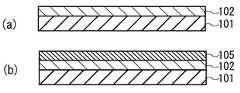
【0003】
図4(a)の符号101は、半導体デバイスを構成するシリコン基板であり、その表面にはシリコン酸化膜102が形成されている。
【0004】
このシリコン基板101をスパッタ装置内に搬入し、アルゴンガスのプラズマを生成し、銅から成るターゲットをスパッタし、シリコン酸化膜102上に銅薄膜を形成し、パターニングして銅配線105を形成する(図4(b))。
【0005】
このようにスパッタ成膜法で形成された銅配線105の比抵抗は、おおよそ2.2μΩcmであり、バルク状態の銅の比抵抗1.7μΩcmに比べて大きくなってしまう。
【0006】
スパッタ装置で銅薄膜を形成した場合、銅薄膜を水素中でアニール処理すれば、形成直後の銅薄膜に比抵抗を小さくできることが知られているが、1.9μΩcm程度までしか小さくならず、不十分である。
【0007】
また、アニール処理をするためには、スパッタ装置とは別に、そのアニール処理のための装置を必要とし、コスト高になるという問題がある。
【0008】
【発明が解決しようとする課題】
本発明は上記従来技術の不都合を解決するために創作されたものであり、その目的は、低抵抗の銅薄膜を提供することにある。
【0009】
【課題を解決するための手段】
本発明の発明者等は、スパッタリングガスのプラズマを発生させ、銅または銅を主成分とするターゲットをスパッタし、成膜対象物表面に銅薄膜を形成する場合に、スパッタ雰囲気中に大気を微少量導入すると、形成された銅薄膜の比抵抗が成膜後の時間の経過とともに低下することを見いだした。
【0010】
特に、添加ガスを5×10⁻⁷Torr(6.65×10⁻⁵Pa)の分圧にしてスパッタした銅薄膜では、成膜後10数時間後にはバルク状態の銅とほぼ等しい値まで比抵抗が低下することを見いだした。
【0011】
本発明は上記知見に基づいて創作されたものであり、請求項1記載の発明は、真空雰囲気中にスパッタガスを導入し、銅または銅を主成分とするターゲットをスパッタし、前記真空雰囲気中に置かれた成膜対象物表面に銅薄膜または銅を主成分とする薄膜を形成する銅薄膜製造方法であって、前記ターゲットをスパッタする際に、添加ガスとして大気を、分圧が1.33×10⁻⁴Pa以下となるように、前記真空雰囲気中に導入することを特徴とする。
請求項2記載の発明は、請求項1記載の銅薄膜製造方法であって、前記添加ガスを間欠的に導入することを特徴とする。
【0012】
本発明は上記のように構成されており、アルゴンガス等のスパッタガス中に、化学構造中に窒素原子、酸素原子、又はその両方の原子を含む添加ガスを所定の分圧で含有させ、スパッタガス及び添加ガスのプラズマを発生させ、銅を主成分とするターゲットをスパッタしている。
【0013】
上記のような添加ガスの導入量は、ガス添加用配管に設けた流量制御バルブを用いて制御し、分圧を6.65×10⁻⁴Pa以下にするのが望ましい。
【0014】
流量制御バルブで制御する場合、その最小制御流量に相当する分圧よりも小さくすることは困難である。従って、添加ガスを流量制御バルブを介して導入する場合に、導入とその停止とを繰り返し、間欠的に導入するようにすると、添加ガスの実効分圧値(時間平均値)を、流量制御バルブで制御できる値よりも小さくすることができる。また、間欠的に導入するタイミングにより、膜界面の組成制御も可能となる。
【0015】
【発明の実施の形態】
本発明のスパッタ装置を、本発明の銅薄膜製造方法と共に説明する。
図1を参照し、符号1は本発明のスパッタ装置の一例であり、真空槽10を有している。真空槽10の底壁側にはカソード装置12が配置されており、天井側には基板ホルダ13が配置されている。
【0016】
カソード装置12はカソード電極22を有しており、その表面(真空槽10の内部側)には銅から成るターゲット21が水平に設けられている。このターゲット21は、基板ホルダ13と対向する位置に配置されている。
【0017】
また、カソード電極22の裏面(真空槽10の外部側)には、ターゲット21表面に磁場を形成するマグネトロン磁石23が配置されている。ターゲット21と基板15の間の距離(T/S)は275mmのいわゆるロングスロースパッタリング(LTS)となっている。
【0018】
真空槽10底壁には、回転軸16が気密に挿通されており、その先端部分には、シャッタ17が取り付けられている。
基板ホルダ13には爪14が設けられており、基板ホルダ13のターゲット21側の面には、爪14によってシリコン基板15が保持されている。
【0019】
真空槽10には、真空排気系18が接続されており、このスパッタ装置1で銅薄膜を形成する際には、真空排気系18によって真空槽10内を真空排気する。真空槽10には、ガス添加用配管31と、スパッタガス導入用配管33とを有するガス導入系3が接続されている。
【0020】
ガス添加用配管31には、流量制御バルブ32が設けられており、端部が大気中に開放されている。スパッタガス導入用配管33は、マスフローコントローラ36を介して、スパッタガスボンベ37に接続されており、真空槽10内にスパッタガスボンベ中37に充填されたスパッタガス(ここではアルゴンガス)を導入できるように構成されている。
【0021】
真空排気系18により、真空槽10内が4×10⁻⁶Torr〜2×10⁻⁷Torrの圧力まで真空排気された後、流量制御バルブ32を操作し、真空槽10内に大気(空気)を添加ガスとして導入する。
【0022】
このときはスパッタガスを導入せず、導入された添加ガスにより、真空槽10内の圧力が上昇し、所定分圧(例えば5×10⁻⁷Torrの分圧)で安定したところで、スパッタガスを導入する。
【0023】
スパッタガスはマスフローコントローラ36によって流量制御しながら導入する(ここでは20sccmの流量で導入した)。このとき、添加ガスの導入量は変えないでおく。
【0024】
スパッタガスの導入により、真空槽10内の圧力が上昇し、5×10⁻⁴Torrの圧力で安定したところで、カソード電極22に負電圧を印加し、ターゲット21表面近傍にプラズマを発生させる。
【0025】
この状態では、シャッタ17はシリコン基板15とターゲット21の間に配置されており、3.7kW(約518V×7.18A)の電力で5分間×2回(2回の間に2分間の放電休止状態を設定する)のプレスパッタを行い、ターゲット21表面をクリーニングし、次いで、回転軸16を回転させ、シリコン基板15とターゲット21の間からシャッタ17を退け、2分後にスパッタを開始すると、シリコン基板15表面に銅薄膜が形成され始める(スパッタ電力は3.17kW)。
【0026】
スパッタを80秒間行い、シリコン基板15表面に約2000Åの銅薄膜を形成した後、カソード電極21への電圧印加を停止すると共に、添加ガス(大気)の導入とスパッタガスの導入を停止し、スパッタを終了させる。基板ホルダ13の温度は、プリスパッタ開始前では30℃であったが、スパッタ終了時には50℃程度に昇温していた。
【0027】
スパッタ終了後、シリコン基板15を取り出し、形成した銅薄膜の比抵抗を測定した。その比抵抗の値は、時間経過に従い小さくなった。
【0028】
図2のグラフに、真空槽10内に導入した添加ガス(ここでは大気)のスパッタガス中の分圧Pと、形成された銅薄膜の比抵抗の経時変化を示す。導入したスパッタガスの流量は20sccmであり、スパッタ雰囲気の圧力は5×10⁻⁴Torrである。添加ガスの分圧Pは、添加ガス導入前の真空槽10の到達圧力P0と、添加ガス導入後の圧力P1との差(P1−P0)で表される。
グラフ中のバルク銅は、銅塊の場合の比抵抗の値である。
【0029】
このグラフから、スパッタ雰囲気中に含まれる添加ガス(大気)の分圧Pを、6.65×10⁻⁴Pa(5×10⁻⁶Torr)以下の大きさにすると効果的であることが分かる。特に、2.66×10⁻⁵Pa(2×10⁻⁷Torr)以下の微小な大きさにすると、形成される銅薄膜の比抵抗は1.7〜1.8μΩcmとなり、バルク銅の値(1.7μΩcm)にほぼ等しくなることがわかる。なお、シリコン表面に熱酸化膜が形成されている基板を用いても同様の結果が得られた。
【0030】
以上は、流量制御バルブ32により、真空槽10内に添加ガスを連続的に導入したが、添加ガスの真空槽10内での分圧Pを一層微小な値にするために、間欠的に導入することができる。
【0031】
例えば、所定の時間間隔で、真空槽10内に間欠的に添加ガス(この添加ガスは化学構造中に酸素原子を有するガス、窒素原子を有するガス、酸素原子と窒素原子を有するガス及び水のいずれか一種以上のガスである。)を微少量導入すると、その分圧を一層小さくすることができる。
【0032】
図3のグラフは、2.5秒間の添加ガス導入を14秒間隔で繰り返し行った場合の真空槽10内の圧力変化を示している。添加ガスの導入により、真空槽10内の圧力はパルス的に2.66×10⁻⁵Pa(2×10⁻⁷Torr)だけ上昇する。
【0033】
このグラフを平均すると、真空槽10内には、1×10⁻⁸〜1×10⁻⁹Torr程度の分圧で添加ガスが含まれていることになる。微小分圧の添加ガスを精度よく導入することは困難であるが、上記のように、間欠的に添加ガスを導入することで達成できる。
【0034】
また、真空槽10内に連続的に添加ガスを導入する配管と、パルス状に添加ガスを導入する配管とを別々に設け、連続的に添加ガスを導入すると共に、そのパルス状の導入を重畳させてもよい。
【0035】
なお、以上は、直流電源を印加してターゲットをスパッタする場合について説明したが、本発明は、交流電圧を印加するRFスパッタ法や、直流電圧に交流電圧を重畳するスパッタ法、直流電圧の大きさを変化させるスパッタ法等、種々のスパッタ法に適用することができる。また、基板ホルダ13に電圧を印加し、シリコン基板15にバイアスを印加したり、フローティングにしてもよい。
【0036】
また、上記の添加ガスには大気(空気)を使用したが、酸素ガス、窒素ガス、又は水分を含有するアルゴンガスであってもよい。酸素ガスと窒素ガスの混合ガスであってもよい。また、酸素ガス、窒素ガス、その混合ガスに水分が含有されるガスであってもよい。
その場合には、ガス添加用配管の端部を流量制御バルブを介して、添加ガスを充填したガスボンベに接続しておくとよい。
【0037】
また、上記はシリコン基板15上に銅薄膜を形成したが、成膜対象物はシリコン基板に限定されるものではない。
【0038】
更にまた、本発明に用いる銅ターゲットは銅から成るターゲット、または銅を主成分とするターゲットであり、銅を主成分とするターゲットは他の金属を含有していてもよい。
【0039】
また、低抵抗化を促進するためにアニールを併用してもよい。ターゲット・基板間の距離は275mmの例を示したが、より短距離のスパッタ装置を用いてもよい。
【0040】
【発明の効果】
銅薄膜の比抵抗を小さくできるので、LSI配線に適している。
添加ガスを間欠的に導入する場合、流量制御バルブで制御可能な値よりも小さい分圧値にすることができる。
銅薄膜形成後、アニール処理をしなくても比抵抗を小さくすることができる。
【図面の簡単な説明】
【図1】本発明の一例のスパッタ装置を示す図
【図2】銅薄膜の比抵抗の経時変化を示すグラフ
【図3】添加ガスを間欠的に導入した場合の圧力変化を示すグラフ
【図4】(a)、(b):銅薄膜の形成方法を説明するための図
【符号の説明】
1……スパッタ装置 10……真空槽 21……ターゲット 31……ガス添加用配管[0001]
BACKGROUND OF THE INVENTION
The present invention relates to the technical field of sputter deposition, and more particularly to the technical field of sputtering a copper or copper-based target to form a copper thin film.
[0002]
[Prior art]
In recent years, a copper thin film having a small specific resistance has attracted attention as a wiring material for semiconductor devices in place of an aluminum thin film.
[0003]
[0004]
This
[0005]
Thus, the specific resistance of the
[0006]
When a copper thin film is formed by a sputtering apparatus, it is known that if the copper thin film is annealed in hydrogen, the specific resistance can be reduced to that of the copper thin film immediately after formation, but it is only reduced to about 1.9 μΩcm. It is enough.
[0007]
In addition, in order to perform the annealing process, an apparatus for the annealing process is required in addition to the sputtering apparatus, and there is a problem that the cost is increased.
[0008]
[Problems to be solved by the invention]
The present invention was created in order to solve the above-described disadvantages of the prior art, and an object thereof is to provide a low-resistance copper thin film.
[0009]
[Means for Solving the Problems]
The inventors of the present invention generate a sputtering gas plasma, sputter a copper or copper-based target, and form a copper thin film on the surface of the film formation object. It has been found that when a small amount is introduced, the specific resistance of the formed copper thin film decreases with the passage of time after film formation.
[0010]
In particular, in the case of a copper thin film sputtered with an additive gas having a partial pressure of 5 × 10⁻⁷ Torr (6.65 ×10⁻⁵Pa ), the ratio is almost equal to that of copper in the bulk state after 10 hours after film formation. I found the resistance to drop.
[0011]
The present invention was created based on the above knowledge, and the invention according to
A second aspect of the present invention is the copper thin film manufacturing method according to the first aspect, wherein the additive gas is introduced intermittently.
[0012]
The present invention is configured as described above, and an sputtering gas such as an argon gas contains an additive gas containing nitrogen atoms, oxygen atoms, or both atoms in the chemical structure at a predetermined partial pressure. Plasma of gas and additive gas is generated to sputter a target mainly composed of copper.
[0013]
The introduction amount of the additive gas as described above is preferably controlled using a flow control valve provided in the gas addition pipe, and the partial pressure is preferably 6.65 × 10⁻⁴ Pa or less.
[0014]
When controlling with a flow control valve, it is difficult to make it smaller than the partial pressure corresponding to the minimum control flow. Therefore, when the additive gas is introduced via the flow control valve, the introduction and the stop thereof are repeated and introduced intermittently, so that the effective partial pressure value (time average value) of the additive gas is calculated as the flow control valve. The value can be made smaller than the value that can be controlled with. Moreover, the composition of the film interface can be controlled by the timing of intermittent introduction.
[0015]
DETAILED DESCRIPTION OF THE INVENTION
The sputtering apparatus of this invention is demonstrated with the copper thin film manufacturing method of this invention.
Referring to FIG. 1,
[0016]
The
[0017]
A
[0018]
A rotating
A
[0019]
A
[0020]
The
[0021]
After the inside of the
[0022]
At this time, without introducing the sputtering gas, the pressure in the
[0023]
The sputtering gas is introduced while controlling the flow rate by the mass flow controller 36 (in this case, it is introduced at a flow rate of 20 sccm). At this time, the introduction amount of the additive gas is not changed.
[0024]
When the sputtering gas is introduced, the pressure in the
[0025]
In this state, the
[0026]
Sputtering was performed for 80 seconds, and after forming a copper thin film of about 2000 mm on the surface of the
[0027]
After the completion of sputtering, the
[0028]
The graph of FIG. 2 shows the change over time in the partial pressure P in the sputtering gas of the additive gas (in this case, the atmosphere) introduced into the
The bulk copper in the graph is a specific resistance value in the case of a copper lump.
[0029]
From this graph, it can be seen that it is effective if the partial pressure P of the additive gas (atmosphere) contained in the sputtering atmosphere is set to 6.65 × 10⁻⁴ Pa (5 × 10⁻⁶ Torr) or less. . In particular, when the microscopic size is 2.66 × 10⁻⁵ Pa (2 × 10⁻⁷ Torr) or less, the specific resistance of the formed copper thin film is 1.7 to 1.8 μΩcm, which is the value of bulk copper ( It can be seen that it is approximately equal to 1.7 μΩcm). Similar results were obtained even when a substrate having a thermal oxide film formed on the silicon surface was used.
[0030]
As described above, the additive gas is continuously introduced into the
[0031]
For example, the additive gas is intermittently added into the
[0032]
The graph of FIG. 3 shows the pressure change in the
[0033]
When this graph is averaged, the
[0034]
In addition, a pipe for continuously introducing the additive gas into the
[0035]
In the above, the case where the target is sputtered by applying a DC power source has been described. However, the present invention can be applied to an RF sputtering method in which an AC voltage is applied, a sputtering method in which an AC voltage is superimposed on a DC voltage, The present invention can be applied to various sputtering methods such as a sputtering method for changing the thickness. Alternatively, a voltage may be applied to the
[0036]
In addition, air (air) is used as the additive gas, but oxygen gas, nitrogen gas, or argon gas containing moisture may be used. It may be a mixed gas of oxygen gas and nitrogen gas. Further, oxygen gas, nitrogen gas, or a gas containing water in the mixed gas may be used.
In that case, the end of the gas addition pipe may be connected to a gas cylinder filled with the additive gas via a flow rate control valve.
[0037]
Moreover, although the above described formed the copper thin film on the
[0038]
Furthermore, the copper target used in the present invention is a target made of copper or a target mainly composed of copper, and the target mainly composed of copper may contain other metals.
[0039]
Further, annealing may be used in combination in order to promote resistance reduction. Although an example in which the distance between the target and the substrate is 275 mm is shown, a shorter-distance sputtering apparatus may be used.
[0040]
【The invention's effect】
Since the specific resistance of the copper thin film can be reduced, it is suitable for LSI wiring.
When the additive gas is introduced intermittently, the partial pressure value can be made smaller than the value controllable by the flow control valve.
After the copper thin film is formed, the specific resistance can be reduced without annealing.
[Brief description of the drawings]
FIG. 1 is a diagram showing a sputtering apparatus according to an example of the present invention. FIG. 2 is a graph showing a change in specific resistance of a copper thin film with time. FIG. 3 is a graph showing a pressure change when an additive gas is intermittently introduced. 4) (a), (b): Diagrams for explaining a method of forming a copper thin film [Explanation of symbols]
1 …… Sputtering
Claims (2)
Translated fromJapanese前記ターゲットをスパッタする際に、添加ガスとして大気を、分圧が1.33×10⁻⁴Pa以下となるように、前記真空雰囲気中に導入することを特徴とする銅薄膜製造方法。A sputtering gas is introduced into a vacuum atmosphere, a copper or copper-based target is sputtered, and a copper thin film or a copper-based thin film is formed on the surface of the film formation target placed in the vacuum atmosphere. A copper thin film manufacturing method,
A method for producing a copper thin film, wherein, when sputtering the target,air is introducedas anadditive gas into the vacuum atmosphereso that apartial pressure is 1.33 × 10⁻⁴Pa or less .
Priority Applications (1)
| Application Number | Priority Date | Filing Date | Title |
|---|---|---|---|
| JP24841799AJP4360716B2 (en) | 1999-09-02 | 1999-09-02 | Copper thin film manufacturing method and sputtering apparatus used in the method |
Applications Claiming Priority (1)
| Application Number | Priority Date | Filing Date | Title |
|---|---|---|---|
| JP24841799AJP4360716B2 (en) | 1999-09-02 | 1999-09-02 | Copper thin film manufacturing method and sputtering apparatus used in the method |
Related Child Applications (1)
| Application Number | Title | Priority Date | Filing Date |
|---|---|---|---|
| JP2008281839ADivisionJP4855455B2 (en) | 2008-10-31 | 2008-10-31 | Copper thin film manufacturing method and sputtering apparatus used in the method |
Publications (2)
| Publication Number | Publication Date |
|---|---|
| JP2001073131A JP2001073131A (en) | 2001-03-21 |
| JP4360716B2true JP4360716B2 (en) | 2009-11-11 |
Family
ID=17177818
Family Applications (1)
| Application Number | Title | Priority Date | Filing Date |
|---|---|---|---|
| JP24841799AExpired - Fee RelatedJP4360716B2 (en) | 1999-09-02 | 1999-09-02 | Copper thin film manufacturing method and sputtering apparatus used in the method |
Country Status (1)
| Country | Link |
|---|---|
| JP (1) | JP4360716B2 (en) |
Families Citing this family (8)
| Publication number | Priority date | Publication date | Assignee | Title |
|---|---|---|---|---|
| JP2004238647A (en)* | 2003-02-04 | 2004-08-26 | Furukawa Techno Research Kk | Smoothed copper foil and method for producing the same |
| EP1862562A1 (en)* | 2006-05-31 | 2007-12-05 | Mec Company Ltd. | Method for manufacturing substrate, and vapor deposition apparatus used for the same |
| KR101059709B1 (en)* | 2006-07-14 | 2011-08-29 | 가부시키가이샤 알박 | Method for manufacturing semiconductor device |
| KR101064144B1 (en)* | 2006-08-10 | 2011-09-15 | 울박, 인크 | A method of forming a conductive film, a thin film transistor, a panel having a thin film transistor, and a manufacturing method of a thin film transistor |
| CN101512730A (en)* | 2006-10-12 | 2009-08-19 | 株式会社爱发科 | Method for forming conductive film, thin film transistor, panel with thin film transistor, and method for manufacturing thin film transistor |
| WO2009131035A1 (en) | 2008-04-25 | 2009-10-29 | 株式会社アルバック | Thin-film transistor manufacturing method, and thin-film transistor |
| CN102471875A (en)* | 2009-07-17 | 2012-05-23 | 株式会社爱发科 | Film-forming apparatus |
| CN102471879B (en)* | 2009-07-17 | 2014-05-07 | 株式会社爱发科 | Film-forming apparatus |
- 1999
- 1999-09-02JPJP24841799Apatent/JP4360716B2/ennot_activeExpired - Fee Related
Also Published As
| Publication number | Publication date |
|---|---|
| JP2001073131A (en) | 2001-03-21 |
Similar Documents
| Publication | Publication Date | Title |
|---|---|---|
| US5510011A (en) | Method for forming a functional deposited film by bias sputtering process at a relatively low substrate temperature | |
| JPS62287071A (en) | Thin film forming device and method | |
| JP2015158014A (en) | Manufacturing method of transparent conductive film, manufacturing apparatus of transparent conductive film, sputtering target, and transparent conductive film | |
| EP4234756A1 (en) | Method for preparing oxide thin film | |
| JP4296256B2 (en) | Manufacturing method of superconducting material | |
| CN109306465B (en) | To Cu3Method for realizing quantitative doping of N film | |
| JP4360716B2 (en) | Copper thin film manufacturing method and sputtering apparatus used in the method | |
| JPH0726198B2 (en) | Thin film forming method and apparatus | |
| JPH06252059A (en) | Method and apparatus for forming film | |
| JPH0641733A (en) | Reactive sputtering equipment | |
| CN117418207B (en) | Three-target high-power pulse magnetron co-sputtering method | |
| JP4855455B2 (en) | Copper thin film manufacturing method and sputtering apparatus used in the method | |
| JPS61193441A (en) | Method of forming metal thin film and therefor device | |
| JPH10298748A (en) | How to deposit golden titanium nitride | |
| US9257291B2 (en) | Method for forming a silicide layer at the bottom of a hole and device for implementing said method | |
| JP2007246993A (en) | Method for forming copper oxide thin film | |
| JP3987617B2 (en) | Contact film barrier film continuous creation device and dissimilar thin film continuous creation device | |
| JP2004137101A (en) | Method for manufacturing titanium oxide film | |
| JP2002030432A (en) | Sputtering apparatus and sputtering method | |
| JP2006032602A (en) | Sputtering apparatus and method | |
| JP3507108B2 (en) | Method of forming deposited film by bias sputtering method | |
| JPH02205674A (en) | Magnetron sputtering device | |
| JPH048506B2 (en) | ||
| JPS634066A (en) | Bias sputtering device | |
| JPH11100670A (en) | Thin film forming apparatus and thin film forming method |
Legal Events
| Date | Code | Title | Description |
|---|---|---|---|
| A621 | Written request for application examination | Free format text:JAPANESE INTERMEDIATE CODE: A621 Effective date:20050805 | |
| A977 | Report on retrieval | Free format text:JAPANESE INTERMEDIATE CODE: A971007 Effective date:20080313 | |
| A131 | Notification of reasons for refusal | Free format text:JAPANESE INTERMEDIATE CODE: A131 Effective date:20080902 | |
| A521 | Written amendment | Free format text:JAPANESE INTERMEDIATE CODE: A523 Effective date:20081031 Free format text:JAPANESE INTERMEDIATE CODE: A821 Effective date:20081031 | |
| TRDD | Decision of grant or rejection written | ||
| A01 | Written decision to grant a patent or to grant a registration (utility model) | Free format text:JAPANESE INTERMEDIATE CODE: A01 Effective date:20090811 | |
| A01 | Written decision to grant a patent or to grant a registration (utility model) | Free format text:JAPANESE INTERMEDIATE CODE: A01 | |
| A61 | First payment of annual fees (during grant procedure) | Free format text:JAPANESE INTERMEDIATE CODE: A61 Effective date:20090811 | |
| R150 | Certificate of patent or registration of utility model | Ref document number:4360716 Country of ref document:JP Free format text:JAPANESE INTERMEDIATE CODE: R150 Free format text:JAPANESE INTERMEDIATE CODE: R150 | |
| FPAY | Renewal fee payment (event date is renewal date of database) | Free format text:PAYMENT UNTIL: 20120821 Year of fee payment:3 | |
| FPAY | Renewal fee payment (event date is renewal date of database) | Free format text:PAYMENT UNTIL: 20130821 Year of fee payment:4 | |
| R250 | Receipt of annual fees | Free format text:JAPANESE INTERMEDIATE CODE: R250 | |
| R250 | Receipt of annual fees | Free format text:JAPANESE INTERMEDIATE CODE: R250 | |
| R250 | Receipt of annual fees | Free format text:JAPANESE INTERMEDIATE CODE: R250 | |
| R250 | Receipt of annual fees | Free format text:JAPANESE INTERMEDIATE CODE: R250 | |
| R250 | Receipt of annual fees | Free format text:JAPANESE INTERMEDIATE CODE: R250 | |
| LAPS | Cancellation because of no payment of annual fees |