JP4358503B2 - Method for manufacturing nonvolatile semiconductor memory device - Google Patents
Method for manufacturing nonvolatile semiconductor memory deviceDownload PDFInfo
- Publication number
- JP4358503B2 JP4358503B2JP2002360872AJP2002360872AJP4358503B2JP 4358503 B2JP4358503 B2JP 4358503B2JP 2002360872 AJP2002360872 AJP 2002360872AJP 2002360872 AJP2002360872 AJP 2002360872AJP 4358503 B2JP4358503 B2JP 4358503B2
- Authority
- JP
- Japan
- Prior art keywords
- gas
- silicon nitride
- nitride film
- insulating film
- hydrogen
- Prior art date
- Legal status (The legal status is an assumption and is not a legal conclusion. Google has not performed a legal analysis and makes no representation as to the accuracy of the status listed.)
- Expired - Fee Related
Links
Images


Classifications
- H—ELECTRICITY
- H10—SEMICONDUCTOR DEVICES; ELECTRIC SOLID-STATE DEVICES NOT OTHERWISE PROVIDED FOR
- H10B—ELECTRONIC MEMORY DEVICES
- H10B41/00—Electrically erasable-and-programmable ROM [EEPROM] devices comprising floating gates
- H10B41/40—Electrically erasable-and-programmable ROM [EEPROM] devices comprising floating gates characterised by the peripheral circuit region
- H10B41/42—Simultaneous manufacture of periphery and memory cells
- H10B41/49—Simultaneous manufacture of periphery and memory cells comprising different types of peripheral transistor
- H—ELECTRICITY
- H10—SEMICONDUCTOR DEVICES; ELECTRIC SOLID-STATE DEVICES NOT OTHERWISE PROVIDED FOR
- H10D—INORGANIC ELECTRIC SEMICONDUCTOR DEVICES
- H10D30/00—Field-effect transistors [FET]
- H10D30/60—Insulated-gate field-effect transistors [IGFET]
- H10D30/68—Floating-gate IGFETs
- H10D30/6891—Floating-gate IGFETs characterised by the shapes, relative sizes or dispositions of the floating gate electrode
- H—ELECTRICITY
- H10—SEMICONDUCTOR DEVICES; ELECTRIC SOLID-STATE DEVICES NOT OTHERWISE PROVIDED FOR
- H10D—INORGANIC ELECTRIC SEMICONDUCTOR DEVICES
- H10D64/00—Electrodes of devices having potential barriers
- H10D64/01—Manufacture or treatment
- H10D64/031—Manufacture or treatment of data-storage electrodes
- H10D64/035—Manufacture or treatment of data-storage electrodes comprising conductor-insulator-conductor-insulator-semiconductor structures
- H—ELECTRICITY
- H10—SEMICONDUCTOR DEVICES; ELECTRIC SOLID-STATE DEVICES NOT OTHERWISE PROVIDED FOR
- H10D—INORGANIC ELECTRIC SEMICONDUCTOR DEVICES
- H10D64/00—Electrodes of devices having potential barriers
- H10D64/60—Electrodes characterised by their materials
- H10D64/66—Electrodes having a conductor capacitively coupled to a semiconductor by an insulator, e.g. MIS electrodes
- H10D64/68—Electrodes having a conductor capacitively coupled to a semiconductor by an insulator, e.g. MIS electrodes characterised by the insulator, e.g. by the gate insulator
- H10D64/681—Electrodes having a conductor capacitively coupled to a semiconductor by an insulator, e.g. MIS electrodes characterised by the insulator, e.g. by the gate insulator having a compositional variation, e.g. multilayered
Landscapes
- Engineering & Computer Science (AREA)
- Manufacturing & Machinery (AREA)
- Semiconductor Memories (AREA)
- Non-Volatile Memory (AREA)
- Insulated Gate Type Field-Effect Transistor (AREA)
- Metal-Oxide And Bipolar Metal-Oxide Semiconductor Integrated Circuits (AREA)
- Formation Of Insulating Films (AREA)
Description
Translated fromJapanese【0001】
【発明の属する技術分野】
本発明は、不揮発性半導体記憶装置の製造方法に関する。更に詳しくは、本発明は、電気的に情報の書き換えが可能な不揮発性半導体記憶装置の製造方法に関する。
【0002】
【従来の技術】
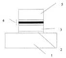
電気的に情報の書き換えが可能な不揮発性半導体記憶装置の内、代表的なフラッシュメモリーについて説明する。フラッシュメモリーは、例えば図7に示すように、半導体基板1上に、第1の絶縁膜2、浮遊ゲートとなる第1のポリシリコン電極3、酸化膜、窒化膜及び酸化膜の積層体からなる第2の絶縁層4、制御ゲートとなる第2のポリシリコン電極5とをこの順で有する。
このフラッシュメモリーでは、第1の絶縁膜2を介してトンネル現象を利用して情報の書き換えを電子の放出・注入により行うため、第1の絶縁膜2はトンネル絶縁膜とも呼ばれる。第1の絶縁膜2は、通常、8〜20nm程度の膜厚を有する。また、ポリシリコン上に高品質で、リーク電流の少ない絶縁膜を形成することは困難である。
【0003】
そのため第2の絶縁層4は、例えば、ポリシリコン酸化膜、CVDシリコン窒化膜、CVDシリコン酸化膜の積層体とし、電界の緩和、制御ゲートと浮遊ゲート間の容量結合を確保しようとしている。上下の酸化膜は、ゲートからの電荷注入に対するバリア層の役割を果たす。中間の窒化膜は、酸化膜よりも比誘電率の高い窒化膜とすることで、物理的な膜厚を確保することができる。更に、酸化膜単層の場合と同等のキャパシタンスを確保しつつ絶縁膜中の電界を緩和することで、酸化膜単層の場合よりもリーク電流の低減を行うことができる。
【0004】
浮遊ゲートを有する不揮発性半導体記憶装置では、制御ゲートの電位を制御することにより、該浮遊ゲート電極と該制御ゲート電極間の容量結合を通じて、浮遊ゲート電極の電位を制御する。図8に浮遊ゲートを有する不揮発性半導体記憶装置の簡略化した等価回路図を示す。ここで、半導体基板1を接地した場合、浮遊ゲートaの電位Vfgは、浮遊ゲートaと制御ゲートb間の容量C1、浮遊ゲートaと半導体基板1間の容量C2、制御ゲート電圧Vcgにより、
Vfg=C1/(C1+C2)×Vcg−Qfg/(C1+C2) (1)
で表される。
【0005】
すなわち、浮遊ゲート電圧は制御ゲート電圧により制御される。浮遊ゲートa内に蓄積された電荷量に応じて、浮遊ゲートaの電位における上式の第2項が変化し、読み出し電流の差となる。この差を読み出し回路によって検出し、メモリセルの記憶状態を判別する。情報の書き換えは、制御ゲートbを介して、半導体基板1と浮遊ゲートa間に高い電圧を発生させて、電子をこの部分の絶縁膜でトンネリングさせることにより、電子の放出、注入を行う。
また、特開2001−160555号公報(特許文献1)には、第2の絶縁膜をラジカル窒化種により形成された窒化膜で使用していること以外は、上記と同様の構造の不揮発性半導体記憶装置が記載されている。
【0006】
【特許文献1】
特開2001−160555号公報
【0007】
【発明が解決しようとする課題】
式(1)において、C1/(C1+C2)は、ゲートカップリング比と呼ばれる。書き換え動作のために必要な一定の浮遊ゲート電圧を得るために必要な制御ゲート電圧は、このゲートカップリング比と逆比例の関係にある。
上記従来例における不揮発性半導体記憶装置において、書き換え電圧には高い電圧が必要である。これは、電子を第1の絶縁膜(トンネル絶縁膜)2を経由して注入する際に、この膜のバンドギャップを越えるエネルギーを電子に与えることができる十分な電圧を制御ゲートに印加することが必要であること、第1の絶縁膜にかかる電圧は、上記ゲートカップリング比に基づくため、更に大きな電圧を半導体基板と制御ゲート間に印加しなければならないことにある。
【0008】
上記浮遊ゲートと制御ゲート間のキャパシタンスが小さいと、ゲートカップリング比が小さくなり、高い電圧を制御ゲートにかける必要がある。このゲートカップリング比を大きくするには、該浮遊ゲートと該制御ゲート間の容量値を上昇させることが有効である。これには、上述の浮遊ゲートと、制御ゲート間のキャパシタ部分の面積を大きく採る方法と、この容量部分の絶縁膜の厚さを薄くする方法がある。
【0009】
前者の方法は、装置の寸法を増大させることになる。そのため、後者の方法が大容量の装置を形成するのに有利である。従来技術では、上述のように、酸化膜/窒化膜/酸化膜の積層体を採用している。上下の酸化膜は、例えば、それぞれ、ポリシリコン上の熱酸化膜と、CVDにより形成された酸化膜である。通常、シリコン基板に形成されるMOSFETのゲート絶縁膜は、面方位が(100)のシリコン単結晶(第2の電極)上に形成した熱酸化膜と比較して絶縁特性が大きく劣る。更に、第1の絶縁膜中の下層の酸化膜を薄膜化すると、第1のポリシリコン電極のコーナー形状部分や、ポリシリコングレイン境界近傍での電界集中により酸化膜に電子(リーク電流)が流れる。この電子が中間層の低圧CVDによる窒化膜中にトラップされる。トラップされた電子は、下層の酸化膜中の電界を強調するので、低電界のバイアス条件下でもこの部分を経由したリーク電流が発生する。同様な現象が第2のポリシリコン電極とその上の上部酸化膜に関しても発生する。また、中間層の窒化膜を薄膜化すると、複合絶縁膜全体の電界を緩和することができなくなり、絶縁特性が単層のポリシリコン酸化膜相当の性能レベルまで劣化してしまう。
【0010】
このように、書き換え電圧の低減のために、従来の方法で第2の絶縁膜を薄膜化すると、該絶縁膜のリーク電流の阻止性能を低く抑制してしまい、フラッシュメモリーの書き換え動作や電荷保持を正しく行うことが困難となる。この結果、ゲートカップリング比を高くできないため、動作電圧の低減が困難な状況にあった。
更に、従来技術でポリシリコン電極上面に形成される酸化膜は、800℃以上で形成される熱酸化膜であった。この800℃以上の熱処理は、下地のポリシリコン電極中にグレインを成長させる。このグレイン成長がポリシリコン電極の表面の凹凸を増大させ、この結果、絶縁膜形成面の平坦性が大きく損なわれていた。そのためキャパシタの微細な凹凸による電界集中により、絶縁性能を損なう傾向があった。
【0011】
また、特開2001−160555号公報に記載されているラジカル窒化種により形成された第2の絶縁層では、ラジカル窒化種により形成された窒化膜のSi−Nの結合が緻密であるほど窒化膜自身の窒化種に対するバリア性が高くなる。そのため窒化種の拡散が阻害され、該窒化膜の成長レートが飽和する傾向があり、任意の膜厚を得ることが困難であった。
【0012】
【課題を解決するための手段】
かくして本発明によれば、シリコン基板上の絶縁膜上に設けられるシリコン原子を含有する第1の電極と、その上に絶縁膜を挟んで形成された第2の電極とを少なくとも備えた構造の不揮発性半導体記憶装置の製造方法であって、絶縁膜が、少なくとも一部に1010cm-2以上の面密度のKrを含有する下部シリコン窒化膜と、上部シリコン窒化膜との少なくとも2層からなり、下部シリコン窒化膜が、Krガス、窒素ガス及び水素ガス、又はKrガス及びNH3ガスを含む雰囲気中で、マイクロ波を導入して雰囲気ガスのプラズマを生成し、第1の電極を窒化することにより形成され、上部シリコン窒化膜が化学気相成長法により形成されることを特徴とする不揮発性半導体記憶装置の製造方法が提供される。
【0014】
【発明の実施の形態】
本発明の不揮発性半導体記憶装置は、シリコン原子を含有する第1の電極と、その上に絶縁膜を挟んで形成された第2の電極とを少なくとも備える。第1の電極は、シリコン原子を含有していさえすれば特に限定されず、例えばポリシリコン層が挙げられる。一方、第2の電極は、例えば、アルミニウム、銅等の金属層、ポリシリコン層、高融点金属(チタン、タングステン等)のシリサイド層、これらの積層体が挙げられる。
【0015】
また、第1の電極は通常、絶縁膜を介して半導体基板上に形成されている。半導体基板としては、特に限定されないが、例えばシリコン基板、シリコンゲルマニウム基板等のシリコン系半導体基板が挙げられる。絶縁膜は、例えば、シリコン酸化膜、シリコン窒化膜、それら膜の積層体等が挙げられる。
また、第1の電極は、半導体基板に溝を形成し、溝表面に絶縁膜を形成し、溝中に第1の電極材料を埋め込み、化学機械研磨法によって電極材料からなる層を平坦化する方法で形成してもよい。
【0016】
本発明では第1と第2の電極間の絶縁膜が、第1の電極側から、第1の電極を窒化することにより得られる下部シリコン窒化膜と、この上に化学気相成長法により形成された上部シリコン窒化膜の少なくとも2層からなる。
更に、下部シリコン窒化膜は、少なくとも一部に1010cm-2以上の面密度の希ガス元素を含有する。また、希ガス元素は、下部シリコン窒化膜の少なくとも一部に含まれていればよく、全面に含まれていてもよい。ここで、希ガス元素は、酸窒化に寄与するラジカル生成効率の観点から、Kr又はArであることが好ましい。なお、希ガス元素の面密度が1010cm-2未満である場合、シリコン窒化膜の化学量論的組成が理想から大きく外れ、シリコン窒化膜の生成レートが大幅に低下し、所望の性能を発揮できないので好ましくない。より好ましい面密度は、1010cm-2以上である。なお、面密度は、2次イオン質量分析計(SIMS)により測定し、希ガスの流量、DCバイアス、RFパワー、真空度等の製造条件を調整することにより所定の値に設定することができる。
【0017】
希ガス元素を含む下部シリコン窒化膜の形成方法は、例えば、窒素ガス又は窒素原子含有化合物ガス及び希ガスを含む雰囲気中で、第1の電極に含まれるシリコン原子を窒化する方法が挙げられる。特に、マイクロ波により雰囲気ガスのプラズマを励起しつつ窒化することが好ましい。
マイクロ波によるプラズマの励起手段としては、マイクロ波を処理室内に導入することができさえすれば特に限定されず公知の方法が使用できる。例えば、ラジアルラインスロットアンテナを用いたプラズマ装置が挙げられる。
【0018】
ここで、窒素原子含有化合物ガスとしては、NH3が挙げられる。また、雰囲気中に、H2を含ませてもよい。
例えば、希ガスがKr、窒素原子含有化合物ガスがNH3の場合、雰囲気中の各ガスの流量比が、90〜99.9%/0.1〜10%(Kr/NH3)であることが好ましい。
供給するマイクロ波の周波数は、900MHz以上、10GHz以下の範囲であることが好ましい。
【0019】
特に、基板温度550℃以下(例えば、200〜550℃)の低温でマイクロ波励起の高密度プラズマを用いて下部シリコン窒化膜を形成することが好ましい。すなわち、第1の電極上に原子状窒化水素NH*(NHラジカルともいう)、あるいは原子状窒素N*(Nラジカルともいう)又はN2+ラジカルと原子状水素H*(Hラジカルともいう)との混合窒化種によりシリコンを直接窒化することにより、1000℃程度の高温で(100)面方位を持つ単結晶Si上に形成したシリコン酸化膜と同等もしくは優れた耐リーク電流特性と、より優れたCharge−to−Breakdown特性を有する薄いシリコン窒化膜を550℃以下(例えば、400〜500℃)という低温で形成することができる。この結果、ポリシリコンのグレイン成長を低温にて十分低く抑制した状態で、リーク電流を低く抑えたまま、ポリシリコン電極間のキャパシタンスを増加させることができる。そのため、ゲートカップリング比が向上し、ひいては、フラッシュメモリーの信頼性を損なうことなく書き換え動作時の印加電圧を大幅に削減することができる。
【0020】
なお、絶縁膜の形成中において、窒素ガスもしくは窒素原子含有化合物ガスの流量比を変えることで、絶縁膜中の窒素濃度ピークを深さ方向に変化させることも可能である。
更に、下部シリコン窒化膜は、形成後、窒素ガス又は窒素原子含有化合物ガスと希ガスを含む雰囲気中で、マイクロ波によりプラズマを励起して形成された原子状窒素水素NH*もしくは原子状窒素N*及び原子状水素H*に曝すことが好ましい。これにより、低温で高品質なシリコン窒化膜を形成することが可能になる。
【0021】
上記工程において、窒素ガス又は窒素原子含有化合物ガスと希ガスは上記下部シリコン窒化膜の形成に使用したのと同じガスを使用することができる。供給するマイクロ波の周波数は、900MHz以上、10GHz以下の範囲であることが好ましい。更に、基板温度550℃以下(例えば、200〜550℃)の低温で行うことが好ましい。
また更に、不揮発性半導体記憶装置がMOSFETを含む周辺回路を備えている場合、上記処理はより好適である。すなわち、MOSFETを構成するゲート絶縁膜を、原子状窒素水素NH*もしくは原子状窒素N*及び原子状水素H*に下部シリコン窒化膜と同時に曝すことで、下部シリコン窒化膜の暴露処理をしつつ、絶縁膜中に窒素原子密度のピークを生じさせることができる。これにより、絶縁膜の不純物に対するバリア性を向上させるとともに、電流に対するバリアハイト、耐絶縁破壊性能を向上させることができる。
【0022】
なお、MOSFETの構造は、ゲート絶縁膜を有する限り特に限定されず、公知の構造を採用することができる。
更に、MOSFETを構成するゲート絶縁膜が、シリコン窒化膜からなる場合、シリコン窒化膜を原子状窒素水素NH*もしくは原子状窒素N*及び原子状水素H*にMOSFETの活性領域を曝すことにより形成することも可能である。また、不揮発性半導体記憶装置が、最上層に最終パッシベーション層を有する場合、下部及び上部シリコン窒化膜を、最終パッシベーション層を形成する前に、500℃以下(具体的には300〜500℃)の水素ラジカル雰囲気に曝すことが好ましい。この処理により、化学気相反応により形成した上部シリコン窒化膜の組成や電気的特性を理想的なシリコン窒化膜に近づけることができる。また、この処理により、下部及び上部シリコン窒化膜や下部シリコン窒化膜/シリコン基板界面から脱離した水素を補填することで、高温処理によるシリコン窒化膜特性の劣化を防止することができる。
【0023】
このように、絶縁膜が、原子状窒素含有種(NH又はNラジカル)によるポリシリコンからなる第1の電極の直接窒化と化学気相反応によるシリコン窒化膜の2層構造であることにより、優れた界面特性と、広い適用膜厚範囲、短い成膜スループットを実現することが可能になる。
更に、Hラジカルを含んだ雰囲気にNラジカル又はN2+ラジカルあるいは、NHラジカルを含有させ、このアニールをメモリセル上だけでなく、周辺回路MOSFET素子の活性領域に作用させることにより、既に配置されたゲート酸化膜に対しては酸化膜の窒化作用を施し、また、シリコン基板に対しては、高性能、高信頼性の極薄窒化膜をシリコンに対する直接窒化によって同時に形成することができる。
【0024】
従来技術では、シリコン酸化膜をシリコン窒化膜に対して複合させることにより、電荷注入に対する障壁高さの確保を図っていた。これに対して、本発明によれば、シリコン窒化膜よりも誘電率において1/2程度しかないために電気的容量の確保に不利なシリコン酸化膜を複合させることなく、シリコン窒化膜のみで絶縁膜を形成することが可能になる。その結果、従来技術よりも、大幅に電気的容量を向上させることができ、不揮発性半導体記憶装置の動作電圧を大きく低減することができる。
従って、上述のような不揮発性半導体記憶装置の動作電圧の低減と、周辺回路デバイスのゲート絶縁膜信頼性・性能の向上を同時に達成することができる。
【0025】
【実施例】
実施例1
まず、プラズマを用いた低温での下部シリコン窒化膜の形成について述べる。図1は、本発明の窒化方法を実現するための、ラジアルラインスロットアンテナを用いた装置の1例を示す概略断面図である。
本実施例においては、窒化膜形成のためにKrを希ガスとして使用する。真空容器(処理室)11内を真空にし、シャワープレート12から、Krガス、NH3ガスを導入し処理室内の圧力を1Torr程度に設定する。シリコンウェーハ等の円形状の基板13を、加熱機構をもつ試料台14にのせ、試料の温度が400℃程度になるように設定する。
【0026】
同軸導波管15から、ラジアルラインスロットアンテナ16、誘電体板17をとおして、処理室11内に2.45GHzのマイクロ波を供給し、処理室11内に高密度のプラズマを生成する。シャワープレート12と基板13の間隔は本実施例では60mmにしてある。この間隔は狭いほうがより高速な成膜が可能になる。上記条件で形成されたシリコン窒化膜は、1010cm-2以上の面密度のKrを含んでいる。
このように、1010cm-2以上の面密度のKrを含むことがシリコン窒化膜の電気的特性、信頼性の改善に寄与している。具体的には、以下の理由により改善されると考えられる。
【0027】
まず、KrとNH3の混合ガスの高密度励起プラズマ中では、中間励起状態にあるKrラジカルにより、NHラジカルが効率よく発生する。このNHラジカルにより基板表面は窒化される。本実施例のシリコン窒化膜によれば、シリコンの面方位を選ばず、(100)面でも(111)面でも(110)面でも低温で高品質なシリコン窒化膜を形成することが可能になる。
【0028】
本発明のシリコン窒化膜においては、プラズマ中に水素ラジカルが存在することが一つの重要な要件である。プラズマ中に水素ラジカルが存在することにより、シリコン窒化膜及び界面のダングリングボンドが、Si−H、N−H結合を形成して終端され、その結果シリコン窒化膜及び界面の電子トラップがなくなる。Si−H結合、N−H結合が本発明のシリコン窒化膜に存在することは、それぞれ赤外吸収スペクトル、X線光電子分光スペクトルを測定することで確認されている。水素が存在することで、CV特性のヒステリシスもなくなる。また、シリコン・シリコン窒化膜界面密度も基板温度を500℃以上にすれば3×1010cm-1と低く抑えられる。
【0029】
なお、KrとN2/H2の混合ガスを使用してシリコン窒化膜を形成する場合には、水素ガスの分圧を0.5%以上とすることで、膜中の電子や正孔のトラップを急激に減少させることができる。この効果は、絶縁膜中にSi−H結合、N−H結合が形成されること、及びKrが含有されることにより実現できる。また、窒化膜中やシリコン/窒化膜界面でのストレスが緩和され、シリコン窒化膜中の固定電荷や界面順位密度が低減されて、電気的特性、信頼性が大幅に改善される。
【0030】
実施例2
本発明をフラッシュメモリーへ適用した構造を図2に示す。図2は、半導体基板1上に第1の絶縁膜2、浮遊ゲートとなる第1のポリシリコン電極3、2層のシリコン窒化膜からなる第2の絶縁層4、制御ゲートとなる第2のポリシリコン電極5をこの順で有する電気的に書き換え可能なフラッシュメモリーである。
【0031】
図2のフラッシュメモリーの製造工程を、図3(a)〜図4(i)の概略工程断面図を用いて示す。断面図では、フラッシュメモリーセルチャンネル領域A、周辺回路高耐圧MOSFET素子領域B、低電圧高性能MOSFET素子領域Cに分けて示している。
まず、半導体基板1上にウエルと、素子分離領域9を形成する。活性領域上の絶縁膜を除去した後、フラッシュメモリーのトンネル酸化膜となる第1の絶縁膜2を10nm程度形成する(図3(a))。
【0032】
次に、浮遊ゲートとなる第1の電極として、ポリシリコン層3aを100nm程度堆積させる(図3(b))。
リソグラフィーによって、浮遊ゲートの領域を画定し、更に、ドライエッチングによって、ポリシリコン層3aをエッチングすることにより、第1のポリシリコン電極3を形成する(図3(c))。
次に、下部シリコン窒化膜4a、上部シリコン窒化膜4bの2層からなる第2の絶縁層4のうち、第1のポリシリコン電極3上に形成される下部シリコン窒化膜4aを形成した(図3(d))。
【0033】
この下部シリコン窒化膜4aは次のようにして形成した。真空容器(処理室)内を真空にし、シャワープレートから、Krガス、N2ガス、H2ガスを導入し、処理室内の圧力を100mTorr程度、半導体基板1の温度が500℃になるように設定した。そして、同軸導波管から、ラジアルラインスロットアンテナ、誘電体板を通して、処理室内に、2.45GHzのマイクロ波を供給して処理室内に高密度のプラズマを生成することで、第1のポリシリコン電極3表面に2〜4nmの下部シリコン窒化膜4aを形成した。この下部シリコン窒化膜4aには、1010cm-2以上の面密度のKrが含まれている。
【0034】
次に、下部シリコン窒化膜4aの上に形成される上部シリコン窒化膜4bは、次のように形成した(図3(e))。処理室内を1Torr以下の低圧にし、半導体基板1を700〜800℃に加熱し、SiClH2ガスとNH3ガスを導入する。これらのガスが反応して、Si3N4からなる上部シリコン窒化膜4bが、第1層目の下部シリコン窒化膜4a上に5nm〜20nm程度堆積される。これは、第2層目の化学気相反応によるSi3N4堆積方法の一例であり、Siの還元ガスと窒素系ガスの反応によりSi3N4を堆積させる反応であれば本実施例に含まれることは言うまでもない。
【0035】
この後、リソグラフィーにより、メモリセルアレイ上にフォトレジスト層6を配し、一方、周辺回路上には、フォトレジスト層6の開口部を設け、これにより、周辺回路部分の上記窒化膜及び酸化膜の除去及び、周辺回路のMOSFET素子の閾値調整のための不純物イオン注入を行う(図4(f))。
フォトレジスト層6を除去した後、基板+全体を酸化雰囲気に曝すことにより、周辺回路MOSFETの活性領域にMOSFET素子のゲート酸化膜7を形成する。また、周辺回路高耐圧MOSFET素子領域Bには、16nm、低電圧高性能MOSFET素子領域Cには、3nmのゲート酸化膜7、8を形成する(図4(g))。
【0036】
その後、基板全体を再度、前述と同様のラジカル窒化雰囲気に曝す(図4(h))。すなわち、真空容器(処理室)内を真空にし、シャワープレートから、Krガス、N2ガス、H2ガスを導入し、処理室内の圧力を100mTorr程度、半導体基板1の温度が500℃になるように設定する。そして、同軸導波管から、ラジアルラインスロットアンテナ、誘電体板を通して、処理室内に、2.45GHzのマイクロ波を供給し、処理室内に高密度のプラズマを生成し、この雰囲気に半導体基板1を暴露する。なお、この処理を、300℃〜500℃の水素ラジカル雰囲気に半導体基板を曝す処理に変えてもよい。
この工程により、メモリセル上のシリコン窒化膜の膜質改善と、周辺回路のゲート酸化膜(7と8)の膜質改善が同時に行われる。
【0037】
その後、フラッシュメモリーの制御ゲートとなる第2の電極材料としてポリシリコン層を100nm程度堆積する。更に、リソグラフィーにより、制御ゲートの領域を画定し、ドライエッチングにより、この電極材料をパターニングして第2のポリシリコン電極5とする(図4(i))。これが、周辺回路領域では、MOSFETのゲート電極になる。
更に、メモリセルと周辺回路MOSFETのソース/ドレイン領域を形成した後、第1の層間絶縁膜を形成、フォトリソグラフィーと異方性ドライエッチングにより、コンタクト孔を形成する。この後、水素ラジカル雰囲気にて300〜500℃の雰囲気にて半導体基板1をアニールする。但し、このアニール工程は、上記のラジカル窒化膜形成後から、最終パッシベーション膜形成までのどの工程に挿入してもよい。更に、配線の形成、層間絶縁膜の形成を繰り返し、最終のパッシベーション膜を形成した後、ワイヤーボンディングパッドの開口部を形成し、工程を終了する。
【0038】
実施例3
本発明の別の実施例を図5(a)〜図6(i)に示す。
半導体基板1上にウエルと、素子分離領域9を形成する。次いで、活性領域上の絶縁膜を除去した後、不揮発性半導体記憶装置のトンネル酸化膜となる第1の絶縁膜2を10nm程度形成する(図5(a))。
次に、浮遊ゲートとなる第1の電極として、ポリシリコン層3aを100nm程度堆積させる(図5(b))。
【0039】
リソグラフィーによって、浮遊ゲートの領域を画定し、更に、ポリシリコン層3aをドライエッチングすることにより、第1のポリシリコン電極3を形成する(図5(c))。
次に、メモリセル領域A上のポリシリコン層3a上の自然酸化膜と周辺回路素子領域B、Cの活性領域における酸化膜を除去した後、下部シリコン窒化膜4a、上部シリコン窒化膜4bからなる第2の絶縁層4を3nm程度形成した(図5(d)、(e))。
【0040】
この下部シリコン窒化膜4aは次のようにして形成した。真空容器(処理室)内を真空にし、シャワープレートから、Krガス、N2ガス、H2ガスを導入し、処理室内の圧力を100mTorr程度、半導体基板1の温度が500℃になるように設定する。そして、同軸導波管から、ラジアルラインスロットアンテナ、誘電体板を通して、処理室内に、2.45GHzのマイクロ波を供給し、処理室内に高密度のプラズマを生成し、ポリシリコン表面に下部シリコン窒化膜4aを形成する。この下部シリコン窒化膜4aには、1010cm-2以上の面密度のKrが含まれている。
【0041】
次に、下部シリコン窒化膜4aの上に形成される上部シリコン窒化膜4bは、次のように形成した。処理室内を1Torr以下の低圧にし、半導体基板1を700〜800℃に加熱し、SiClH2ガスとNH3ガスを導入する。これらのガスが反応して、Si3N4が第1層目の下部シリコン窒化膜4a上に5nm〜20nm程度堆積して上部シリコン窒化膜となる。これは、第2層目の化学気相反応によるSi3N4堆積方法の一例であり、Siの還元ガスと窒素系ガスの反応によりSi3N4を堆積させる反応であれば本実施例に含まれることは言うまでもない。
【0042】
この後、リソグラフィーを用いたフォトレジスト層6により、周辺回路領域の低電圧駆動MOSFETを形成する領域Cの上記シリコン窒化膜を除去する(図6(f))。更に、周辺回路のMOSFET素子領域に対して、閾値電圧調整用の不純物イオン注入を行う。フォトレジスト層6を除去した後(図6(g))、基板全体を再度、前述と同様のラジカル窒化雰囲気に曝す(図6(h))。すなわち、真空容器(処理室)内を真空にし、シャワープレートから、Krガス、N2ガス、H2ガスを導入し、処理室内の圧力を100mTorr程度、半導体基板1の温度が500℃になるように設定する。そして、同軸導波管から、ラジアルラインスロットアンテナ、誘電体板を通して、処理室内に、2.45GHzのマイクロ波を供給し、処理室内に高密度のプラズマを生成し、この雰囲気に半導体基板を暴露する。このアニール条件は、単結晶シリコン上に2〜8nm程度の直接シリコン窒化膜を形成する程度の処理条件とする。
【0043】
これにより、周辺回路領域の高耐圧MOSFET領域の活性領域には、半導体基板1上の第2の絶縁膜に更にラジカル窒化雰囲気による改善作用が加わったシリコン窒化膜が容量値の酸化膜換算の膜厚で4〜11.5nm形成される。また、低電圧駆動MOSFET領域には、ラジカル窒化雰囲気による容量値の酸化膜換算の膜厚で1〜4nmのシリコン窒化膜のみが形成される。その後に、ラジカル水素アニールを施してもよい。
その後、不揮発性記憶装置の制御ゲートとなる第2の電極材料としてポリシリコン層を100nm程度堆積し、リソグラフィーにより、制御ゲートの領域を定義し、ドライエッチングにより、この電極材料をパターニングして第2のポリシリコン電極5とする(図6(i))。これが、周辺回路領域では、MOSFETのゲート電極になる。
【0044】
更に、断面図からは省略しているが、メモリセルと周辺回路MOSFETのソース/ドレイン領域を形成した後、第1の層間絶縁膜を形成、フォトリソグラフィーと異方性ドライエッチングにより、コンタクト孔を形成する。この後、水素ラジカル雰囲気にて300〜500℃の雰囲気にて半導体基板1をアニールする。但し、このアニール工程は、上記のラジカル窒化膜形成後から、最終パッシベーション膜形成までのどの工程に挿入してもよい。更に、配線の形成、層間絶縁膜の形成を繰り返し、最終のパッシベーション膜を形成した後、ワイヤーボンディングパッドの開口部を形成し、工程を終了する。
【0045】
【発明の効果】
本発明によれば、第1の電極(浮遊ゲート)と第2の電極(制御ゲート)間の絶縁膜が、第1の電極側から、第1の電極を窒化することにより得られる下部シリコン窒化膜と、この上に化学気相成長法により形成された上部シリコン窒化膜の少なくとも2層からなり、下部シリコン窒化膜が、少なくとも一部に1010cm-2以上の面密度の希ガス原子を含有することで、低電圧で書き換え可能な電荷保持特性の優れた高品質で、高性能な不揮発性半導体記憶装置を得ることが可能になる。
【図面の簡単な説明】
【図1】ラジアルスロットアンテナを用いたプラズマ装置の概略概念図である。
【図2】本発明の第1の実施例によるフラッシュメモリーセル概略断面図である。
【図3】本発明の第1の実施例における製造工程の概略断面図である。
【図4】本発明の第1の実施例における製造工程の概略断面図である。
【図5】本発明の第2の実施例における製造工程の概略断面図である。
【図6】本発明の第2の実施例における製造工程の概略断面図である。
【図7】従来例におけるフラッシュメモリーの概略断面図である。
【図8】浮遊ゲートを有する不揮発性メモリーの簡略化した等価回路図である。
【符号の説明】
1 半導体基板
2 第1の絶縁膜
3 第1のポリシリコン電極
3a ポリシリコン層
4a 下部シリコン窒化膜
4b 上部シリコン窒化膜
4 第2の絶縁層
5 第2のポリシリコン電極
6 フォトレジスト層
7、8 ゲート酸化膜
9 素子分離領域
11 真空容器(処理室)
12 シャワープレート
13 基板
14 試料台
15 同軸導波管
16 ラジアルラインスロットアンテナ
17 誘電体板
A フラッシュメモリーセルチャンネル領域
B 周辺回路高耐圧MOSFET素子領域
C 低電圧高性能MOSFET素子領域
a 浮遊ゲート
b 制御ゲート[0001]
BACKGROUND OF THE INVENTION
The present invention relates to a nonvolatile semiconductor memory device.SetIt relates to a manufacturing method. More specifically, the present invention relates to a nonvolatile semiconductor memory device that can electrically rewrite information.SetIt relates to a manufacturing method.
[0002]
[Prior art]
A typical flash memory among the nonvolatile semiconductor memory devices capable of electrically rewriting information will be described. For example, as shown in FIG. 7, the flash memory includes a first
In this flash memory, information is rewritten by electron emission / injection using the tunnel phenomenon through the first
[0003]
Therefore, the second
[0004]
In a nonvolatile semiconductor memory device having a floating gate, the potential of the floating gate electrode is controlled through capacitive coupling between the floating gate electrode and the control gate electrode by controlling the potential of the control gate. FIG. 8 shows a simplified equivalent circuit diagram of a nonvolatile semiconductor memory device having a floating gate. Here, when the
Vfg = C1 / (C1 + C2) × Vcg−Qfg / (C1 + C2) (1)
It is represented by
[0005]
That is, the floating gate voltage is controlled by the control gate voltage. In accordance with the amount of charge accumulated in the floating gate a, the second term in the above equation at the potential of the floating gate a changes, resulting in a difference in read current. This difference is detected by the reading circuit, and the storage state of the memory cell is determined. Information is rewritten by emitting and injecting electrons by generating a high voltage between the
Japanese Patent Laid-Open No. 2001-160555 (Patent Document 1) discloses a non-volatile semiconductor having a structure similar to the above except that the second insulating film is a nitride film formed of radical nitriding species. A storage device is described.
[0006]
[Patent Document 1]
JP 2001-160555 A
[0007]
[Problems to be solved by the invention]
In the formula (1), C1 / (C1 + C2) is called a gate coupling ratio. The control gate voltage required to obtain a certain floating gate voltage required for the rewrite operation is in an inversely proportional relationship with the gate coupling ratio.
In the nonvolatile semiconductor memory device in the above conventional example, a high voltage is required for the rewrite voltage. This is because, when electrons are injected through the first insulating film (tunnel insulating film) 2, a sufficient voltage that can give the electrons energy exceeding the band gap of this film is applied to the control gate. This is because the voltage applied to the first insulating film is based on the gate coupling ratio, so that a larger voltage must be applied between the semiconductor substrate and the control gate.
[0008]
When the capacitance between the floating gate and the control gate is small, the gate coupling ratio becomes small, and it is necessary to apply a high voltage to the control gate. In order to increase the gate coupling ratio, it is effective to increase the capacitance value between the floating gate and the control gate. This includes a method of increasing the area of the capacitor portion between the floating gate and the control gate, and a method of reducing the thickness of the insulating film of the capacitance portion.
[0009]
The former method increases the size of the device. Therefore, the latter method is advantageous for forming a large capacity device. In the prior art, as described above, a laminated body of oxide film / nitride film / oxide film is employed. The upper and lower oxide films are, for example, a thermal oxide film on polysilicon and an oxide film formed by CVD. Usually, a gate insulating film of a MOSFET formed on a silicon substrate is greatly inferior in insulating properties as compared with a thermal oxide film formed on a silicon single crystal (second electrode) having a plane orientation of (100). Further, when the lower oxide film in the first insulating film is thinned, electrons (leakage current) flow to the oxide film due to the electric field concentration near the corner shape portion of the first polysilicon electrode and the polysilicon grain boundary. . These electrons are trapped in the nitride film formed by the low pressure CVD of the intermediate layer. Since the trapped electrons emphasize the electric field in the underlying oxide film, a leak current is generated via this portion even under a low electric field bias condition. A similar phenomenon occurs with respect to the second polysilicon electrode and the upper oxide film thereon. Further, if the nitride film of the intermediate layer is made thinner, the electric field of the entire composite insulating film cannot be relaxed, and the insulating characteristics deteriorate to a performance level equivalent to that of a single-layer polysilicon oxide film.
[0010]
Thus, if the second insulating film is thinned by the conventional method to reduce the rewriting voltage, the leakage current blocking performance of the insulating film is suppressed to a low level, and the flash memory rewriting operation and charge retention are suppressed. It is difficult to do correctly. As a result, since the gate coupling ratio cannot be increased, it is difficult to reduce the operating voltage.
Furthermore, the oxide film formed on the upper surface of the polysilicon electrode in the prior art is a thermal oxide film formed at 800 ° C. or higher. The heat treatment at 800 ° C. or higher grows grains in the underlying polysilicon electrode. This grain growth increases the unevenness of the surface of the polysilicon electrode, and as a result, the flatness of the insulating film formation surface is greatly impaired. For this reason, there has been a tendency to deteriorate the insulation performance due to the electric field concentration due to the minute unevenness of the capacitor.
[0011]
Further, in the second insulating layer formed by radical nitriding species described in Japanese Patent Application Laid-Open No. 2001-160555, the more dense the Si—N bond of the nitride film formed by radical nitriding species, the more the nitride film The barrier property against its own nitriding species is increased. Therefore, diffusion of nitriding species is hindered, and the growth rate of the nitride film tends to be saturated, and it is difficult to obtain an arbitrary film thickness.
[0012]
[Means for Solving the Problems]
Thus, according to the present invention, a structure having at least a first electrode containing silicon atoms provided on an insulating film on a silicon substrate and a second electrode formed on the insulating film on the first electrode is provided. Nonvolatile semiconductor memory deviceManufacturing methodAnd the insulating film isAt least some 10Tencm-2The lower silicon nitride film includes at least two layers of a lower silicon nitride film containing Kr having the above surface density and an upper silicon nitride film. The lower silicon nitride film is composed of Kr gas, nitrogen gas and hydrogen gas, or Kr gas and NH.ThreeIn a gas-containing atmosphere, microwaves are introduced to generate plasma of the atmospheric gas, and the first electrode is formed by nitriding, and an upper silicon nitride film is formed by chemical vapor deposition.Nonvolatile semiconductor memory deviceManufacturing methodIs provided.
[0014]
DETAILED DESCRIPTION OF THE INVENTION
The nonvolatile semiconductor memory device of the present invention includes at least a first electrode containing silicon atoms and a second electrode formed thereon with an insulating film interposed therebetween. The first electrode is not particularly limited as long as it contains silicon atoms, and examples thereof include a polysilicon layer. On the other hand, examples of the second electrode include a metal layer such as aluminum and copper, a polysilicon layer, a silicide layer of a refractory metal (titanium, tungsten, etc.), and a laminate thereof.
[0015]
The first electrode is usually formed on the semiconductor substrate via an insulating film. Although it does not specifically limit as a semiconductor substrate, For example, silicon system semiconductor substrates, such as a silicon substrate and a silicon germanium substrate, are mentioned. Examples of the insulating film include a silicon oxide film, a silicon nitride film, and a laminate of these films.
The first electrode includes a groove formed in the semiconductor substrate, an insulating film is formed on the groove surface, the first electrode material is embedded in the groove, and a layer made of the electrode material is planarized by a chemical mechanical polishing method. It may be formed by a method.
[0016]
In the present invention, an insulating film between the first and second electrodes is formed from the first electrode side by a chemical vapor deposition method on a lower silicon nitride film obtained by nitriding the first electrode. The upper silicon nitride film is composed of at least two layers.
Further, the lower silicon nitride film is at least partially 10.Tencm-2It contains a rare gas element having the above surface density. Further, the rare gas element may be included in at least a part of the lower silicon nitride film, and may be included in the entire surface. Here, the rare gas element is preferably Kr or Ar from the viewpoint of radical generation efficiency contributing to oxynitridation. The surface density of the rare gas element is 10Tencm-2If it is less than the range, the stoichiometric composition of the silicon nitride film deviates greatly from the ideal, and the generation rate of the silicon nitride film is greatly reduced, and the desired performance cannot be exhibited. A more preferable areal density is 10Tencm-2That's it. The areal density is measured by a secondary ion mass spectrometer (SIMS), and can be set to a predetermined value by adjusting manufacturing conditions such as a rare gas flow rate, a DC bias, an RF power, and a degree of vacuum. .
[0017]
Examples of the method for forming the lower silicon nitride film containing a rare gas element include a method of nitriding silicon atoms contained in the first electrode in an atmosphere containing nitrogen gas or a nitrogen atom-containing compound gas and a rare gas. In particular, it is preferable to perform nitridation while exciting the atmosphere gas plasma with microwaves.
As a means for exciting the plasma by the microwave, any known method can be used as long as the microwave can be introduced into the processing chamber. For example, a plasma apparatus using a radial line slot antenna can be mentioned.
[0018]
Here, as the nitrogen atom-containing compound gas, NHThreeIs mentioned. In the atmosphere, H2May be included.
For example, the rare gas is Kr, and the nitrogen atom-containing compound gas is NH.Three, The flow rate ratio of each gas in the atmosphere is 90-99.9% / 0.1-10% (Kr / NHThree) Is preferable.
The frequency of the supplied microwave is preferably in the range of 900 MHz to 10 GHz.
[0019]
In particular, it is preferable to form the lower silicon nitride film by using microwave-excited high-density plasma at a substrate temperature of 550 ° C. or lower (for example, 200 to 550 ° C.). That is, atomic hydrogen nitride NH * (also referred to as NH radical), atomic nitrogen N * (also referred to as N radical) or N on the first electrode2+Silicon oxide film formed on single crystal Si having a (100) plane orientation at a high temperature of about 1000 ° C. by directly nitriding silicon with a mixed nitriding species of radical and atomic hydrogen H * (also referred to as H radical) Can be formed at a low temperature of 550 ° C. or lower (for example, 400 to 500 ° C.) with a leakage current characteristic equivalent to or better than that of the present invention and a better charge-to-breakdown characteristic. As a result, it is possible to increase the capacitance between the polysilicon electrodes while keeping the leakage current low while keeping the grain growth of the polysilicon sufficiently low at a low temperature. As a result, the gate coupling ratio is improved, and as a result, the applied voltage during the rewrite operation can be significantly reduced without degrading the reliability of the flash memory.
[0020]
Note that during the formation of the insulating film, the nitrogen concentration peak in the insulating film can be changed in the depth direction by changing the flow ratio of the nitrogen gas or the nitrogen atom-containing compound gas.
Further, after forming the lower silicon nitride film, atomic nitrogen hydrogen NH * or atomic nitrogen N formed by exciting plasma with microwaves in an atmosphere containing nitrogen gas or a nitrogen atom-containing compound gas and a rare gas. Exposure to * and atomic hydrogen H * is preferred. This makes it possible to form a high-quality silicon nitride film at a low temperature.
[0021]
In the above process, the same gas as that used for forming the lower silicon nitride film can be used as the nitrogen gas or the nitrogen atom-containing compound gas and the rare gas. The frequency of the supplied microwave is preferably in the range of 900 MHz to 10 GHz. Furthermore, it is preferable to carry out at a low temperature of a substrate temperature of 550 ° C. or lower (for example, 200 to 550 ° C.).
Furthermore, when the nonvolatile semiconductor memory device includes a peripheral circuit including a MOSFET, the above process is more preferable. That is, by exposing the gate insulating film constituting the MOSFET to atomic nitrogen hydrogen NH * or atomic nitrogen N * and atomic hydrogen H * simultaneously with the lower silicon nitride film, the lower silicon nitride film is exposed. A peak of nitrogen atom density can be generated in the insulating film. Thereby, the barrier property against the impurities of the insulating film can be improved, and the barrier height against the current and the dielectric breakdown resistance can be improved.
[0022]
Note that the structure of the MOSFET is not particularly limited as long as it has a gate insulating film, and a known structure can be adopted.
Further, when the gate insulating film constituting the MOSFET is made of a silicon nitride film, the silicon nitride film is formed by exposing the active region of the MOSFET to atomic nitrogen hydrogen NH * or atomic nitrogen N * and atomic hydrogen H *. It is also possible to do. Further, when the nonvolatile semiconductor memory device has the final passivation layer as the uppermost layer, the lower and upper silicon nitride films are formed at a temperature of 500 ° C. or lower (specifically, 300 to 500 ° C.) before forming the final passivation layer. Exposure to a hydrogen radical atmosphere is preferred. By this treatment, the composition and electrical characteristics of the upper silicon nitride film formed by the chemical vapor reaction can be brought close to an ideal silicon nitride film. Also, by this treatment, hydrogen desorbed from the lower and upper silicon nitride films and the lower silicon nitride film / silicon substrate interface can be compensated to prevent deterioration of silicon nitride film characteristics due to high temperature processing.
[0023]
Thus, the insulating film is excellent in that it has a two-layer structure of direct nitridation of the first electrode made of polysilicon by atomic nitrogen-containing species (NH or N radical) and silicon nitride film by chemical vapor reaction. It is possible to realize the interface characteristics, a wide range of applied film thickness, and a short film formation throughput.
Further, N radical or N in an atmosphere containing H radical2+By incorporating radicals or NH radicals and applying this annealing not only to the memory cell but also to the active region of the peripheral circuit MOSFET element, the gate oxide film already disposed is subjected to nitridation of the oxide film. In addition, a high-performance and highly reliable ultra-thin nitride film can be simultaneously formed on a silicon substrate by direct nitridation on silicon.
[0024]
In the prior art, a barrier height against charge injection is secured by combining a silicon oxide film with a silicon nitride film. On the other hand, according to the present invention, since the dielectric constant is only about ½ of that of the silicon nitride film, the silicon oxide film is insulated only from the silicon nitride film without compounding the silicon oxide film which is disadvantageous for securing the electric capacity. A film can be formed. As a result, the electric capacity can be greatly improved as compared with the prior art, and the operating voltage of the nonvolatile semiconductor memory device can be greatly reduced.
Therefore, it is possible to simultaneously reduce the operating voltage of the nonvolatile semiconductor memory device as described above and improve the reliability and performance of the gate insulating film of the peripheral circuit device.
[0025]
【Example】
Example 1
First, formation of the lower silicon nitride film using plasma at a low temperature will be described. FIG. 1 is a schematic cross-sectional view showing an example of an apparatus using a radial line slot antenna for realizing the nitriding method of the present invention.
In this embodiment, Kr is used as a rare gas for forming a nitride film. The inside of the vacuum vessel (processing chamber) 11 is evacuated, and from the
[0026]
A microwave of 2.45 GHz is supplied from the
Thus, 10Tencm-2The inclusion of Kr with the above surface density contributes to the improvement of the electrical characteristics and reliability of the silicon nitride film. Specifically, it is considered that this is improved for the following reasons.
[0027]
First, Kr and NHThreeIn the high density excitation plasma of the mixed gas, NH radicals are efficiently generated by Kr radicals in an intermediate excitation state. The substrate surface is nitrided by this NH radical. According to the silicon nitride film of this embodiment, it is possible to form a high-quality silicon nitride film at a low temperature regardless of the plane orientation of silicon, regardless of the (100) plane, (111) plane, or (110) plane. .
[0028]
In the silicon nitride film of the present invention, the presence of hydrogen radicals in the plasma is one important requirement. Due to the presence of hydrogen radicals in the plasma, dangling bonds at the silicon nitride film and the interface are terminated by forming Si—H and N—H bonds, and as a result, there are no electron traps at the silicon nitride film and the interface. The presence of Si—H bonds and N—H bonds in the silicon nitride film of the present invention has been confirmed by measuring an infrared absorption spectrum and an X-ray photoelectron spectrum, respectively. The presence of hydrogen eliminates the hysteresis of CV characteristics. Also, the silicon / silicon nitride film interface density is 3 × 10 3 if the substrate temperature is 500 ° C. or higher.Tencm-1And low.
[0029]
Kr and N2/ H2When a silicon nitride film is formed using a mixed gas of hydrogen, trapping of electrons and holes in the film can be drastically reduced by setting the partial pressure of hydrogen gas to 0.5% or more. . This effect can be realized by forming Si—H bonds and N—H bonds in the insulating film and containing Kr. In addition, the stress at the nitride film or at the silicon / nitride film interface is alleviated, the fixed charge in the silicon nitride film and the interface order density are reduced, and the electrical characteristics and reliability are greatly improved.
[0030]
Example 2
A structure in which the present invention is applied to a flash memory is shown in FIG. 2 shows a first
[0031]
The manufacturing process of the flash memory of FIG. 2 will be described with reference to the schematic process cross-sectional views of FIGS. 3 (a) to 4 (i). In the sectional view, the flash memory cell channel region A, the peripheral circuit high voltage MOSFET element region B, and the low voltage high performance MOSFET element region C are shown separately.
First, a well and an element isolation region 9 are formed on the
[0032]
Next, a
The region of the floating gate is defined by lithography, and the
Next, the lower
[0033]
The lower
[0034]
Next, the upper
[0035]
Thereafter, a photoresist layer 6 is disposed on the memory cell array by lithography, while an opening of the photoresist layer 6 is provided on the peripheral circuit, whereby the nitride film and oxide film in the peripheral circuit portion are formed. Removal and impurity ion implantation for adjusting the threshold value of the MOSFET elements in the peripheral circuit are performed (FIG. 4F).
After the photoresist layer 6 is removed, a
[0036]
Thereafter, the entire substrate is again exposed to the same radical nitriding atmosphere as described above (FIG. 4H). That is, the inside of the vacuum vessel (processing chamber) is evacuated and the Kr gas, N2Gas, H2Gas is introduced, the pressure in the processing chamber is set to about 100 mTorr, and the temperature of the
By this step, the film quality of the silicon nitride film on the memory cell and the film quality of the gate oxide films (7 and 8) in the peripheral circuit are simultaneously improved.
[0037]
Thereafter, a polysilicon layer is deposited to a thickness of about 100 nm as a second electrode material that becomes a control gate of the flash memory. Furthermore, the region of the control gate is defined by lithography, and this electrode material is patterned by dry etching to form the second polysilicon electrode 5 (FIG. 4 (i)). This becomes the gate electrode of the MOSFET in the peripheral circuit region.
Further, after the source / drain regions of the memory cell and the peripheral circuit MOSFET are formed, a first interlayer insulating film is formed, and contact holes are formed by photolithography and anisotropic dry etching. Thereafter, the
[0038]
Example 3
Another embodiment of the present invention is shown in FIGS. 5 (a) to 6 (i).
A well and an element isolation region 9 are formed on the
Next, a
[0039]
The region of the floating gate is defined by lithography, and the
Next, after removing the natural oxide film on the
[0040]
The lower
[0041]
Next, the upper
[0042]
Thereafter, the silicon nitride film in the region C where the low voltage driving MOSFET is formed in the peripheral circuit region is removed by the photoresist layer 6 using lithography (FIG. 6F). Further, impurity ion implantation for adjusting the threshold voltage is performed on the MOSFET element region of the peripheral circuit. After removing the photoresist layer 6 (FIG. 6G), the entire substrate is again exposed to a radical nitriding atmosphere similar to that described above (FIG. 6H). That is, the inside of the vacuum vessel (processing chamber) is evacuated and the Kr gas, N2Gas, H2Gas is introduced, the pressure in the processing chamber is set to about 100 mTorr, and the temperature of the
[0043]
Thereby, in the active region of the high breakdown voltage MOSFET region in the peripheral circuit region, the silicon nitride film in which the improvement action by the radical nitriding atmosphere is further added to the second insulating film on the
Thereafter, a polysilicon layer is deposited to a thickness of about 100 nm as a second electrode material to be a control gate of the nonvolatile memory device, a control gate region is defined by lithography, and this electrode material is patterned by dry etching to form a second electrode material. The
[0044]
Further, although omitted from the sectional view, after forming the source / drain regions of the memory cell and the peripheral circuit MOSFET, a first interlayer insulating film is formed, and contact holes are formed by photolithography and anisotropic dry etching. Form. Thereafter, the
[0045]
【The invention's effect】
According to the present invention, the insulating film between the first electrode (floating gate) and the second electrode (control gate) is the lower silicon nitride obtained by nitriding the first electrode from the first electrode side. A film, and at least two layers of an upper silicon nitride film formed thereon by chemical vapor deposition, and the lower silicon nitride film is at least partially 10Tencm-2By containing the rare gas atoms having the above surface density, it is possible to obtain a high-quality and high-performance nonvolatile semiconductor memory device having excellent charge retention characteristics that can be rewritten at a low voltage.
[Brief description of the drawings]
FIG. 1 is a schematic conceptual diagram of a plasma apparatus using a radial slot antenna.
FIG. 2 is a schematic cross-sectional view of a flash memory cell according to a first embodiment of the present invention.
FIG. 3 is a schematic cross-sectional view of the manufacturing process in the first embodiment of the present invention.
FIG. 4 is a schematic sectional view of a manufacturing process in the first embodiment of the present invention.
FIG. 5 is a schematic cross-sectional view of a manufacturing process in the second embodiment of the present invention.
FIG. 6 is a schematic cross-sectional view of a manufacturing process in the second embodiment of the present invention.
FIG. 7 is a schematic cross-sectional view of a flash memory in a conventional example.
FIG. 8 is a simplified equivalent circuit diagram of a non-volatile memory having a floating gate.
[Explanation of symbols]
1 Semiconductor substrate
2 First insulating film
3 First polysilicon electrode
3a Polysilicon layer
4a Lower silicon nitride film
4b Upper silicon nitride film
4 Second insulating layer
5 Second polysilicon electrode
6 Photoresist layer
7, 8 Gate oxide film
9 Element isolation region
11 Vacuum container (processing chamber)
12 Shower plate
13 Substrate
14 Sample table
15 Coaxial waveguide
16 Radial line slot antenna
17 Dielectric plate
A Flash memory cell channel area
B Peripheral circuit high voltage MOSFET element region
C Low voltage high performance MOSFET device area
a Floating gate
b Control gate
Claims (5)
Translated fromJapanesePriority Applications (2)
| Application Number | Priority Date | Filing Date | Title |
|---|---|---|---|
| JP2002360872AJP4358503B2 (en) | 2002-12-12 | 2002-12-12 | Method for manufacturing nonvolatile semiconductor memory device |
| US10/732,475US6969885B2 (en) | 2002-12-12 | 2003-12-11 | Non-volatile semiconductor memory device with first and second nitride insulators |
Applications Claiming Priority (1)
| Application Number | Priority Date | Filing Date | Title |
|---|---|---|---|
| JP2002360872AJP4358503B2 (en) | 2002-12-12 | 2002-12-12 | Method for manufacturing nonvolatile semiconductor memory device |
Publications (2)
| Publication Number | Publication Date |
|---|---|
| JP2004193413A JP2004193413A (en) | 2004-07-08 |
| JP4358503B2true JP4358503B2 (en) | 2009-11-04 |
Family
ID=32588128
Family Applications (1)
| Application Number | Title | Priority Date | Filing Date |
|---|---|---|---|
| JP2002360872AExpired - Fee RelatedJP4358503B2 (en) | 2002-12-12 | 2002-12-12 | Method for manufacturing nonvolatile semiconductor memory device |
Country Status (2)
| Country | Link |
|---|---|
| US (1) | US6969885B2 (en) |
| JP (1) | JP4358503B2 (en) |
Families Citing this family (13)
| Publication number | Priority date | Publication date | Assignee | Title |
|---|---|---|---|---|
| WO2003015151A1 (en)* | 2001-08-02 | 2003-02-20 | Tokyo Electron Limited | Base material treating method and electron device-use material |
| US7335941B2 (en)* | 2004-07-14 | 2008-02-26 | Taiwan Semiconductor Manufacturing Company, Ltd. | Uniform channel programmable erasable flash EEPROM |
| CN101069274B (en) | 2005-04-15 | 2010-05-19 | 东京毅力科创株式会社 | Method for manufacturing semiconductor device and plasma nitriding method |
| JP4734019B2 (en) | 2005-04-26 | 2011-07-27 | 株式会社東芝 | Semiconductor memory device and manufacturing method thereof |
| JP5386058B2 (en)* | 2005-04-28 | 2014-01-15 | 株式会社半導体エネルギー研究所 | Method for manufacturing semiconductor device |
| CN101194345B (en)* | 2005-06-08 | 2010-05-19 | 国立大学法人东北大学 | Plasma nitriding method and apparatus, and semiconductor device manufacturing method |
| JP2007188969A (en)* | 2006-01-11 | 2007-07-26 | Toshiba Corp | Semiconductor device and manufacturing method thereof |
| JP2007288069A (en)* | 2006-04-19 | 2007-11-01 | Hitachi Kokusai Electric Inc | Manufacturing method of semiconductor device |
| JP5408930B2 (en)* | 2007-08-31 | 2014-02-05 | 株式会社半導体エネルギー研究所 | Method for manufacturing semiconductor device |
| JP5232425B2 (en)* | 2007-09-10 | 2013-07-10 | ルネサスエレクトロニクス株式会社 | Nonvolatile semiconductor memory device and manufacturing method thereof |
| TWI489528B (en)* | 2011-07-12 | 2015-06-21 | Winbond Electronics Corp | Method of fabricating memory |
| US10383489B2 (en) | 2012-02-10 | 2019-08-20 | Gpcp Ip Holdings Llc | Automatic napkin dispenser |
| EP4128353A4 (en)* | 2020-07-30 | 2023-10-25 | Yangtze Memory Technologies Co., Ltd. | THREE-DIMENSIONAL STORAGE DEVICE WITH HYDROGEN-RICH SEMICONDUCTOR CHANNELS |
Family Cites Families (1)
| Publication number | Priority date | Publication date | Assignee | Title |
|---|---|---|---|---|
| JP4397491B2 (en) | 1999-11-30 | 2010-01-13 | 財団法人国際科学振興財団 | Semiconductor device using silicon having 111 plane orientation on surface and method of forming the same |
- 2002
- 2002-12-12JPJP2002360872Apatent/JP4358503B2/ennot_activeExpired - Fee Related
- 2003
- 2003-12-11USUS10/732,475patent/US6969885B2/ennot_activeExpired - Lifetime
Also Published As
| Publication number | Publication date |
|---|---|
| US6969885B2 (en) | 2005-11-29 |
| JP2004193413A (en) | 2004-07-08 |
| US20040119111A1 (en) | 2004-06-24 |
Similar Documents
| Publication | Publication Date | Title |
|---|---|---|
| US7109083B2 (en) | Flash memory device and a fabrication process thereof, method of forming a dielectric film | |
| JP5068402B2 (en) | Dielectric film and method for forming the same, semiconductor device, nonvolatile semiconductor memory device, and method for manufacturing semiconductor device | |
| JP4713752B2 (en) | Semiconductor device and manufacturing method thereof | |
| US7119407B2 (en) | Semiconductor device and manufacturing method thereof | |
| JP2004031760A (en) | Semiconductor device and method of manufacturing the same | |
| JP2004153037A (en) | Method for manufacturing semiconductor device | |
| JP4358503B2 (en) | Method for manufacturing nonvolatile semiconductor memory device | |
| US8270216B2 (en) | Semiconductor storage device and method of manufacturing the same | |
| TW200915494A (en) | Semiconductor memory device, and manufacturing method thereof | |
| JP4358504B2 (en) | Method for manufacturing nonvolatile semiconductor memory device | |
| JP5313547B2 (en) | Manufacturing method of semiconductor device | |
| US20070267706A1 (en) | Formation of low leakage thermally assisted radical nitrided dielectrics | |
| KR20070058725A (en) | Manufacturing method of nonvolatile memory device | |
| JP2000332014A (en) | Insulating film |
Legal Events
| Date | Code | Title | Description |
|---|---|---|---|
| A621 | Written request for application examination | Free format text:JAPANESE INTERMEDIATE CODE: A621 Effective date:20050615 | |
| A977 | Report on retrieval | Free format text:JAPANESE INTERMEDIATE CODE: A971007 Effective date:20071109 | |
| A131 | Notification of reasons for refusal | Free format text:JAPANESE INTERMEDIATE CODE: A131 Effective date:20071113 | |
| A521 | Request for written amendment filed | Free format text:JAPANESE INTERMEDIATE CODE: A523 Effective date:20080115 | |
| A131 | Notification of reasons for refusal | Free format text:JAPANESE INTERMEDIATE CODE: A131 Effective date:20090512 | |
| A521 | Request for written amendment filed | Free format text:JAPANESE INTERMEDIATE CODE: A523 Effective date:20090713 | |
| TRDD | Decision of grant or rejection written | ||
| A01 | Written decision to grant a patent or to grant a registration (utility model) | Free format text:JAPANESE INTERMEDIATE CODE: A01 Effective date:20090804 | |
| A01 | Written decision to grant a patent or to grant a registration (utility model) | Free format text:JAPANESE INTERMEDIATE CODE: A01 | |
| A61 | First payment of annual fees (during grant procedure) | Free format text:JAPANESE INTERMEDIATE CODE: A61 Effective date:20090806 | |
| FPAY | Renewal fee payment (event date is renewal date of database) | Free format text:PAYMENT UNTIL: 20120814 Year of fee payment:3 | |
| R150 | Certificate of patent or registration of utility model | Ref document number:4358503 Country of ref document:JP Free format text:JAPANESE INTERMEDIATE CODE: R150 Free format text:JAPANESE INTERMEDIATE CODE: R150 | |
| FPAY | Renewal fee payment (event date is renewal date of database) | Free format text:PAYMENT UNTIL: 20120814 Year of fee payment:3 | |
| FPAY | Renewal fee payment (event date is renewal date of database) | Free format text:PAYMENT UNTIL: 20130814 Year of fee payment:4 | |
| S111 | Request for change of ownership or part of ownership | Free format text:JAPANESE INTERMEDIATE CODE: R313115 | |
| R371 | Transfer withdrawn | Free format text:JAPANESE INTERMEDIATE CODE: R371 | |
| S111 | Request for change of ownership or part of ownership | Free format text:JAPANESE INTERMEDIATE CODE: R313115 | |
| R350 | Written notification of registration of transfer | Free format text:JAPANESE INTERMEDIATE CODE: R350 | |
| LAPS | Cancellation because of no payment of annual fees |