JP4356114B2 - Stage apparatus, exposure apparatus, and device manufacturing method - Google Patents
Stage apparatus, exposure apparatus, and device manufacturing methodDownload PDFInfo
- Publication number
- JP4356114B2 JP4356114B2JP2005504935AJP2005504935AJP4356114B2JP 4356114 B2JP4356114 B2JP 4356114B2JP 2005504935 AJP2005504935 AJP 2005504935AJP 2005504935 AJP2005504935 AJP 2005504935AJP 4356114 B2JP4356114 B2JP 4356114B2
- Authority
- JP
- Japan
- Prior art keywords
- gas
- frame
- reticle
- reticle stage
- axis
- Prior art date
- Legal status (The legal status is an assumption and is not a legal conclusion. Google has not performed a legal analysis and makes no representation as to the accuracy of the status listed.)
- Expired - Fee Related
Links
Images


Classifications
- G—PHYSICS
- G03—PHOTOGRAPHY; CINEMATOGRAPHY; ANALOGOUS TECHNIQUES USING WAVES OTHER THAN OPTICAL WAVES; ELECTROGRAPHY; HOLOGRAPHY
- G03F—PHOTOMECHANICAL PRODUCTION OF TEXTURED OR PATTERNED SURFACES, e.g. FOR PRINTING, FOR PROCESSING OF SEMICONDUCTOR DEVICES; MATERIALS THEREFOR; ORIGINALS THEREFOR; APPARATUS SPECIALLY ADAPTED THEREFOR
- G03F7/00—Photomechanical, e.g. photolithographic, production of textured or patterned surfaces, e.g. printing surfaces; Materials therefor, e.g. comprising photoresists; Apparatus specially adapted therefor
- G03F7/70—Microphotolithographic exposure; Apparatus therefor
- G03F7/70058—Mask illumination systems
- H—ELECTRICITY
- H01—ELECTRIC ELEMENTS
- H01L—SEMICONDUCTOR DEVICES NOT COVERED BY CLASS H10
- H01L21/00—Processes or apparatus adapted for the manufacture or treatment of semiconductor or solid state devices or of parts thereof
- H01L21/02—Manufacture or treatment of semiconductor devices or of parts thereof
- H01L21/027—Making masks on semiconductor bodies for further photolithographic processing not provided for in group H01L21/18 or H01L21/34
- H01L21/0271—Making masks on semiconductor bodies for further photolithographic processing not provided for in group H01L21/18 or H01L21/34 comprising organic layers
- H01L21/0273—Making masks on semiconductor bodies for further photolithographic processing not provided for in group H01L21/18 or H01L21/34 comprising organic layers characterised by the treatment of photoresist layers
- H01L21/0274—Photolithographic processes
- G—PHYSICS
- G03—PHOTOGRAPHY; CINEMATOGRAPHY; ANALOGOUS TECHNIQUES USING WAVES OTHER THAN OPTICAL WAVES; ELECTROGRAPHY; HOLOGRAPHY
- G03F—PHOTOMECHANICAL PRODUCTION OF TEXTURED OR PATTERNED SURFACES, e.g. FOR PRINTING, FOR PROCESSING OF SEMICONDUCTOR DEVICES; MATERIALS THEREFOR; ORIGINALS THEREFOR; APPARATUS SPECIALLY ADAPTED THEREFOR
- G03F7/00—Photomechanical, e.g. photolithographic, production of textured or patterned surfaces, e.g. printing surfaces; Materials therefor, e.g. comprising photoresists; Apparatus specially adapted therefor
- G03F7/70—Microphotolithographic exposure; Apparatus therefor
- G03F7/70691—Handling of masks or workpieces
- G03F7/70716—Stages
- G—PHYSICS
- G03—PHOTOGRAPHY; CINEMATOGRAPHY; ANALOGOUS TECHNIQUES USING WAVES OTHER THAN OPTICAL WAVES; ELECTROGRAPHY; HOLOGRAPHY
- G03F—PHOTOMECHANICAL PRODUCTION OF TEXTURED OR PATTERNED SURFACES, e.g. FOR PRINTING, FOR PROCESSING OF SEMICONDUCTOR DEVICES; MATERIALS THEREFOR; ORIGINALS THEREFOR; APPARATUS SPECIALLY ADAPTED THEREFOR
- G03F7/00—Photomechanical, e.g. photolithographic, production of textured or patterned surfaces, e.g. printing surfaces; Materials therefor, e.g. comprising photoresists; Apparatus specially adapted therefor
- G03F7/70—Microphotolithographic exposure; Apparatus therefor
- G03F7/70691—Handling of masks or workpieces
- G03F7/70758—Drive means, e.g. actuators, motors for long- or short-stroke modules or fine or coarse driving
- G—PHYSICS
- G03—PHOTOGRAPHY; CINEMATOGRAPHY; ANALOGOUS TECHNIQUES USING WAVES OTHER THAN OPTICAL WAVES; ELECTROGRAPHY; HOLOGRAPHY
- G03F—PHOTOMECHANICAL PRODUCTION OF TEXTURED OR PATTERNED SURFACES, e.g. FOR PRINTING, FOR PROCESSING OF SEMICONDUCTOR DEVICES; MATERIALS THEREFOR; ORIGINALS THEREFOR; APPARATUS SPECIALLY ADAPTED THEREFOR
- G03F7/00—Photomechanical, e.g. photolithographic, production of textured or patterned surfaces, e.g. printing surfaces; Materials therefor, e.g. comprising photoresists; Apparatus specially adapted therefor
- G03F7/70—Microphotolithographic exposure; Apparatus therefor
- G03F7/70691—Handling of masks or workpieces
- G03F7/70766—Reaction force control means, e.g. countermass
- H—ELECTRICITY
- H01—ELECTRIC ELEMENTS
- H01L—SEMICONDUCTOR DEVICES NOT COVERED BY CLASS H10
- H01L21/00—Processes or apparatus adapted for the manufacture or treatment of semiconductor or solid state devices or of parts thereof
- H01L21/67—Apparatus specially adapted for handling semiconductor or electric solid state devices during manufacture or treatment thereof; Apparatus specially adapted for handling wafers during manufacture or treatment of semiconductor or electric solid state devices or components ; Apparatus not specifically provided for elsewhere
- H01L21/68—Apparatus specially adapted for handling semiconductor or electric solid state devices during manufacture or treatment thereof; Apparatus specially adapted for handling wafers during manufacture or treatment of semiconductor or electric solid state devices or components ; Apparatus not specifically provided for elsewhere for positioning, orientation or alignment
Landscapes
- Physics & Mathematics (AREA)
- General Physics & Mathematics (AREA)
- Engineering & Computer Science (AREA)
- Microelectronics & Electronic Packaging (AREA)
- Manufacturing & Machinery (AREA)
- Computer Hardware Design (AREA)
- Condensed Matter Physics & Semiconductors (AREA)
- Power Engineering (AREA)
- Chemical & Material Sciences (AREA)
- Chemical Kinetics & Catalysis (AREA)
- Exposure And Positioning Against Photoresist Photosensitive Materials (AREA)
- Exposure Of Semiconductors, Excluding Electron Or Ion Beam Exposure (AREA)
- Container, Conveyance, Adherence, Positioning, Of Wafer (AREA)
- Linear Motors (AREA)
- Reciprocating, Oscillating Or Vibrating Motors (AREA)
Description
Translated fromJapanese本発明は、ステージ装置及び露光装置、並びにデバイス製造方法に係り、更に詳しくは、定盤と、該定盤に沿って移動するスライダとを備えるステージ装置、該ステージ装置を備える露光装置、並びに前記露光装置を用いるデバイス製造方法に関する。 The present invention relates to a stage apparatus, an exposure apparatus, and a device manufacturing method. More specifically, the present invention relates to a stage apparatus that includes a surface plate and a slider that moves along the surface plate, an exposure apparatus that includes the stage apparatus, and The present invention relates to a device manufacturing method using an exposure apparatus.
近年、半導体素子、液晶表示素子等を製造するリソグラフィ工程においては、マスク又はレチクル(以下、「レチクル」と総称する)とウエハ又はガラスプレート等の感光物体(以下、「ウエハ」と総称する)とを所定の走査方向(スキャン方向)に沿って同期移動しつつ、レチクルのパターンを投影光学系を介してウエハ上に転写する、ステップ・アンド・スキャン方式の走査型露光装置(いわゆるスキャニング・ステッパ(スキャナ)とも呼ばれる)などが比較的多く用いられるようになってきた。走査型露光装置は、ステッパなどの静止型露光装置に比べると、大フィールドをより小さな投影光学系で露光できる。このため、走査型露光装置には、投影光学系の製造が容易であるとともに、大フィールド露光によるショット数の減少により高スループットが期待でき、さらに投影光学系に対してレチクル及び基板を相対走査することで平均化効果があり、ディストーションや焦点深度の向上が期待できる等の種々のメリットがある。 In recent years, in a lithography process for manufacturing a semiconductor element, a liquid crystal display element, and the like, a mask or a reticle (hereinafter collectively referred to as “reticle”) and a photosensitive object such as a wafer or a glass plate (hereinafter collectively referred to as “wafer”). Is a step-and-scan type scanning exposure apparatus (a so-called scanning stepper) that transfers a reticle pattern onto a wafer via a projection optical system while synchronously moving along a predetermined scanning direction (scanning direction). Relatively often used are also called scanners). The scanning exposure apparatus can expose a large field with a smaller projection optical system than a stationary exposure apparatus such as a stepper. For this reason, in the scanning exposure apparatus, it is easy to manufacture the projection optical system, and a high throughput can be expected by reducing the number of shots by large field exposure, and the reticle and substrate are scanned relative to the projection optical system. Thus, there are various merits such as an averaging effect and an improvement in distortion and depth of focus.
しかるに、走査型露光装置では、ウエハ側に加え、レチクル側にも、レチクルを駆動する駆動装置が必要である。最近の走査型露光装置では、レチクル側の駆動装置として、レチクル定盤上にエアベアリング等により浮上支持され、走査方向に直交する非走査方向(非スキャン方向)の両側に配置された1対のリニアモータによって、走査方向に所定ストローク範囲で駆動されるレチクル粗動ステージと、該レチクル粗動ステージに対して、スキャン方向及び非スキャン方向及びヨーイング方向にボイスコイルモータ等によって微少駆動されるレチクル微動ステージとを有する粗微動構造のレチクルステージ装置が用いられている。 However, in the scanning exposure apparatus, a drive device for driving the reticle is required on the reticle side in addition to the wafer side. In a recent scanning type exposure apparatus, as a reticle side driving device, a pair of air bearings and the like which are levitated and supported on a reticle surface plate and arranged on both sides in a non-scanning direction (non-scanning direction) perpendicular to the scanning direction. A reticle coarse movement stage driven by a linear motor in a predetermined stroke range in the scanning direction, and a reticle fine movement slightly driven by a voice coil motor or the like in the scanning direction, non-scanning direction and yawing direction with respect to the reticle coarse movement stage. A reticle stage apparatus having a coarse / fine movement structure having a stage is used.
また、レチクルステージの駆動に応じてリニアモータの固定子に生じる反力がレチクル定盤の振動要因や姿勢変化の要因となるのを極力抑制するため、前記反力を受けて、運動量保存則に従って、例えばレチクルステージのスキャン方向に延設されたリニアモータの固定子(リニアガイド)に沿って、レチクルステージとは反対方向に移動するカウンタマス(錘部材)を有するカウンタマス機構が設けられたレチクルステージ装置もある。 In addition, in order to suppress the reaction force generated in the stator of the linear motor according to the driving of the reticle stage from being a factor of vibration of the reticle surface plate and a factor of posture change as much as possible, in response to the reaction force, the law of conservation of momentum For example, a reticle provided with a counter mass mechanism having a counter mass (weight member) that moves in a direction opposite to the reticle stage along a stator (linear guide) of a linear motor extended in the scanning direction of the reticle stage. There is also a stage device.
しかしながら、従来の走査型露光装置が採用するレチクルステージ装置では、以下のような改善すべき点が種々存在する。
a. 微動ステージ駆動用のモータの固定子が設けられた固定子キャリアと定盤との間にサイドガイドがあるため、レチクル微動ステージ(レチクル)の非スキャン方向の位置決め時の反力及びヨーイングモーメント、並びに粗動ステージの駆動時に生じるモーメントが、サイドガイドを介して定盤に伝達され、これが定盤の振動要因となり、結果的にレチクルの位置制御精度(位置決め精度を含む)を悪化させていた。
b. レチクル微動ステージ及びレチクル粗動ステージには、電流供給のための配線や、バキュームチャックのための真空排気用の配管及びエアベアリングに対する加圧空気の供給用の配管などが接続されていた。このため、レチクル微動ステージ及びレチクル粗動ステージが移動する際には、上記の配線、配管が引きずられ、それら配線、配管の張力が、結果的にレチクルの位置制御精度(位置決め精度を含む)を悪化させる要因となっていた。
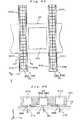
c. レチクル微動ステージ周辺の機械的な振動、熱的要因によるステージ曲げがレチクル微動ステージの位置計測誤差の要因となっていた。一例として、図12(A)に示されるように、レチクル微動ステージRSTに設けられた移動鏡169を介してレチクル微動ステージRST(レチクルR)の位置を測長軸LXを有する干渉計で測定する場合について考える。この場合において、レチクルステージRSTに図12(B)に示されるような変形が生じたものとすると、干渉計によって計測される位置情報にΔMの計測誤差(一種のアッベ誤差)が生じることとなる。なお、図12(A)、図12(B)において、符号CRは、レチクル微動ステージRSTの中立面(曲げ中立面)を示す。
d. さらに、レチクル微動ステージの変形が、移動鏡の変形(曲がり)要因となり、レチクル微動ステージの位置計測精度、ひいては位置制御精度の低下を招いていた。
e. また、特にカウンタマス機構を備えるレチクルステージ装置では、カウンタマス(錘部材)とレチクルステージとの質量比を十分大きく確保することが困難であった。その理由は、上記従来のカウンタマス機構では、カウンタマスはリニアガイドの軸上に重心を配置する必要があるため、カウンタマスの質量を大きくするためには、カウンタマスをリニアガイドの軸方向に延長するか、リニアガイドを中心として軸直交面内で放射方向の距離が一律に大きくなるようにする必要があり、レイアウトの都合上、自ずと制限があるためである。このようにカウンタマス(錘部材)とレチクルステージとの質量比を十分大きく確保することが困難であったことから、カウンタマスのストロークが大きくなり、配管を引きずることの影響や、重心移動による局部的なボディ変形が無視できず、位置制御性の低下の要因となっていた。
f. この他、レチクルステージの周辺部材の配置、形状などが複雑で、その周辺空間は入り組んだ開放空間となっていたため、空調効率が悪く、空気揺らぎ(空気の温度揺らぎ)などによって干渉計計測精度、ひいてはレチクルの位置制御性を悪化させる要因ともなっていた。さらに、F2レーザなどの真空紫外光を露光用照明光として用いる場合には、レチクル周辺においても雰囲気気体を不活性ガスで置換するガスパージを行わなければならないが、上記のレチクルステージの周辺部材の配置、形状などの複雑化のために、その設計が非常に困難なものとなっていた。However, the reticle stage apparatus employed by the conventional scanning exposure apparatus has various points to be improved as follows.
a. Because there is a side guide between the stator carrier and the surface plate where the stator of the motor for driving the fine movement stage is provided, the reaction force and yawing moment when positioning the reticle fine movement stage (reticle) in the non-scanning direction, and A moment generated during driving of the coarse movement stage is transmitted to the surface plate via the side guide, which becomes a vibration factor of the surface plate, resulting in deterioration of reticle position control accuracy (including positioning accuracy).
b. The reticle fine movement stage and the reticle coarse movement stage were connected with wiring for supplying current, piping for evacuation for the vacuum chuck, piping for supplying pressurized air to the air bearing, and the like. For this reason, when the reticle fine movement stage and the reticle coarse movement stage move, the wiring and piping are dragged, and the tension of the wiring and piping results in the reticle position control accuracy (including positioning accuracy). It was a factor to make it worse.
c. The mechanical vibration around the reticle fine movement stage and stage bending due to thermal factors have caused the position measurement error of the reticle fine movement stage. As an example, as shown in FIG. 12A, the position of the reticle fine movement stage RST (reticle R) is measured by an interferometer having a length measuring axis LX via a moving
d. Further, the deformation of the reticle fine movement stage causes the deformation (bending) of the movable mirror, leading to a decrease in the position measurement accuracy of the reticle fine movement stage and consequently the position control accuracy.
e. In particular, in a reticle stage apparatus including a counter mass mechanism, it is difficult to ensure a sufficiently large mass ratio between the counter mass (weight member) and the reticle stage. The reason is that in the conventional counter mass mechanism, the counter mass needs to have a center of gravity on the axis of the linear guide. Therefore, in order to increase the mass of the counter mass, the counter mass is arranged in the axial direction of the linear guide. This is because the distance in the radial direction needs to be extended uniformly in the axis orthogonal plane with the linear guide as the center, and there is a limitation due to the layout. Since it was difficult to secure a sufficiently large mass ratio between the counter mass (weight member) and the reticle stage in this way, the stroke of the counter mass was increased, the effect of dragging the piping, The body deformation was not negligible, which caused a decrease in position controllability.
f. In addition, the arrangement and shape of the peripheral members of the reticle stage are complicated, and the surrounding space is an intricate open space. Therefore, the air conditioning efficiency is poor, and the interferometer measurement accuracy due to air fluctuation (air temperature fluctuation), etc. As a result, the position controllability of the reticle is also deteriorated. Further, when vacuum ultraviolet light such as F2 laser is used as the illumination light for exposure, a gas purge for replacing the atmospheric gas with an inert gas must be performed around the reticle. Due to the complexity of the arrangement and shape, the design has become very difficult.
本発明は、かかる事情の下になされたもので、その第1の目的は、特に、物体が載置される移動体の位置制御性の向上を図ることができるステージ装置を提供することにある。 The present invention has been made under such circumstances, and a first object thereof is to provide a stage apparatus capable of improving the position controllability of a moving body on which an object is placed. .
また、本発明の第2の目的は、高精度な露光を実現することが可能な露光装置を提供することにある。 A second object of the present invention is to provide an exposure apparatus capable of realizing highly accurate exposure.
また、本発明の第3の目的は、高集積度のデバイスの生産性を向上させることが可能なデバイス製造方法を提供することにある。 A third object of the present invention is to provide a device manufacturing method capable of improving the productivity of a highly integrated device.
本発明は、第1の観点からすると、定盤と;前記定盤の上方に浮上しつつ物体を保持して第1軸及びこれに直交する第2軸を含む2次元面内の3自由度方向に前記定盤に沿って移動可能なスライダと;前記定盤の上方に浮上しつつ前記2次元面内の3自由度を少なくとも有し、前記スライダを取り囲む枠状部材と;前記枠状部材に設けられた第1固定子と、該第1固定子と協働して前記スライダを前記第1軸方向に駆動する駆動力を発生する第1可動子とを含む第1駆動機構と;前記枠状部材に設けられた第2固定子と、前記第2固定子と協働して前記スライダを前記第2軸方向に駆動する駆動力を発生する第2可動子とを含む第2駆動機構と;を備えるステージ装置である。From a first viewpoint, the present invention provides a three-degree-of-freedom in a two-dimensional plane that includes a surface plate; a first axis that floats above the surface plate, and a second axis that is orthogonal to the first axis. A slider movable in the direction along the surface plate; a frame-shaped member that floats above the surface plate and has at least three degrees of freedom in the two-dimensional plane and surrounds the slider; and the frame-shaped member A first drive mechanism comprising: a first stator provided on the first stator; and a first mover that generates a driving force for driving the slider in the first axial direction in cooperation with the first stator; A second drive mechanism including a second stator provided on the frame-shaped member and a second mover that generates a driving force for driving the slider in the second axial direction in cooperation with the second stator. When; isabsent stage apparatus comprising a.
ここで、固定子と可動子とが「協働する」とは、固定子と可動子との間の何らかの物理的相互作用(例えば電気磁気的な相互作用など)を行って駆動力を発生することを意味する。本明細書では、かかる意味で協働なる用語を用いるものとする。 Here, the “cooperating” between the stator and the mover means that some physical interaction (for example, an electromagnetic interaction) is generated between the stator and the mover to generate a driving force. Means that. In this specification, the term which cooperates in this meaning shall be used.
これによれば、スライダは、定盤の上方に浮上しつつ物体を保持して第1軸及びこれに直交する第2軸を含む2次元面内の3自由度方向に前記定盤に沿って移動可能であり、枠状部材は、定盤の上方に浮上しつつ前記2次元面内の3自由度を少なくとも有している。枠状部材には、第1固定子、第2固定子が設けられ、第1固定子と協働してスライダを第1軸方向に駆動する駆動力を発生する第1可動子、第2固定子と協働してスライダを第2軸方向に駆動する駆動力を発生する第2可動子がスライダに設けられている。従って、スライダが第1駆動機構又は第2駆動機構により第1軸方向又は第2軸方向に駆動されると、その駆動力に応じた反力が第1固定子又は第2固定子に生じる(作用する)。この反力の作用により枠状部材が、運動量保存則にほぼ従って、2次元面内の3自由度方向に移動する。すなわち、枠状部材がカウンタマスの役目を果たす。この場合、枠状部材の移動により、前記反力がほぼ完全にキャンセルされるとともに、スライダ及び枠状部材を含む系の重心移動が生じないので、定盤には偏荷重も作用しない。従って、物体が載置されるスライダの位置制御性の向上を図ることができる。また、この場合、枠状部材はスライダを取り囲む状態で設けられているので、必然的に大型化し、その質量が大きくなり、枠状部材とスライダとの大きな質量比を確保することができ、枠状部材の移動ストロークは比較的短くて足りる。また、枠状部材を大型化する場合に、その支障は殆どない。 According to this, the slider holds the object while floating above the surface plate, and moves along the surface plate in the direction of three degrees of freedom in a two-dimensional plane including the first axis and the second axis perpendicular thereto. The frame member is movable and has at least three degrees of freedom in the two-dimensional plane while floating above the surface plate. The frame-shaped member is provided with a first stator and a second stator, and cooperates with the first stator to generate a driving force for driving the slider in the first axial direction. A second mover that generates a driving force for driving the slider in the second axial direction in cooperation with the child is provided on the slider. Accordingly, when the slider is driven in the first axial direction or the second axial direction by the first driving mechanism or the second driving mechanism, a reaction force corresponding to the driving force is generated in the first stator or the second stator ( Act). The action of the reaction force causes the frame-like member to move in the direction of three degrees of freedom in the two-dimensional plane almost in accordance with the momentum conservation law. That is, the frame-shaped member serves as a counter mass. In this case, the reaction force is almost completely canceled by the movement of the frame-like member, and the center of gravity of the system including the slider and the frame-like member does not move, so that no offset load acts on the surface plate. Therefore, the position controllability of the slider on which the object is placed can be improved. In this case, since the frame-shaped member is provided so as to surround the slider, the size is inevitably increased, the mass thereof is increased, and a large mass ratio between the frame-shaped member and the slider can be secured. The movement stroke of the member is relatively short. Moreover, there is almost no hindrance when the frame-like member is enlarged.
この場合において、第1駆動機構、第2駆動機構の構成は種々考えられるが、例えば前記第1駆動機構は、少なくとも2つのリニアモータを含み、前記第2駆動機構は、少なくとも1つのボイスコイルモータを含むこととすることができる。 In this case, various configurations of the first drive mechanism and the second drive mechanism can be considered. For example, the first drive mechanism includes at least two linear motors, and the second drive mechanism includes at least one voice coil motor. Can be included.
本発明のステージ装置では、前記スライダの位置を計測する干渉計システムを更に備え、前記スライダには、中立面の一部に前記物体の載置面が形成されるとともに、前記干渉計システムからの測長ビームの光路の前記2次元面に直交する第3軸方向の位置が前記中立面の位置に一致していることとすることができる。かかる場合には、前述の図12(B)を用いて説明した、スライダの変形の際に中立面と測長軸とのずれに起因して生じる位置計測誤差ΔMを略零にすることができる。Instages apparatusof the present invention further comprises an interferometer system for measuring the position of the slider, the slider, with the mounting surface of the object is formed on a part of the neutral plane, the interferometer system The position in the third axis direction orthogonal to the two-dimensional plane of the optical path of the measurement beam from the second axis coincides with the position of the neutral plane. In such a case, the position measurement error ΔM generated due to the deviation between the neutral surface and the length measuring axis when the slider is deformed as described with reference to FIG. it can.
本発明のステージ装置では、前記スライダの第1軸方向の一側及び他側の端部には第1軸方向に延びる延設部がそれぞれ設けられ、前記一側の延設部から他側の延設部に至る長手方向の全域に渡る気体静圧軸受が形成され、前記定盤から配管を介さないで前記気体静圧軸受に対して加圧気体が供給されることとすることができる。Instages apparatusof the present invention, the at the end of the one side and the other side of the first axis direction of the slider is provided extending portion extending in a first axial direction, respectively, the other side from the extending portion of the one side A gas static pressure bearing is formed over the entire region in the longitudinal direction leading to the extending portion of the gas, and pressurized gas can be supplied from the surface plate to the gas static pressure bearing without a pipe. .
本発明は、第2の観点からすると、マスクと感光物体とを所定方向に同期移動して前記マスクに形成されたパターンを前記感光物体に転写する露光装置であって、前記マスクを照明光により照明する照明ユニットと;前記マスクが前記物体として前記スライダ上に載置される本発明のステージ装置と;前記マスクから射出される前記照明光を前記感光物体上に投射する投影光学系ユニットと;を備える露光装置である。According to a second aspect of the present invention, there is provided an exposure apparatus for transferring a pattern formed on the mask onto the photosensitive object by synchronously moving the mask and the photosensitive object in a predetermined direction, wherein the mask is illuminated with illumination light. an illumination unit for illuminating; a projection optical system unit that projects the illumination light emitted from the mask onto the photosensitive object; the maskstages apparatusand the present invention is placed on the slider as the object ; anexposure lightunit Ru provided with.
これによれば、本発明のステージ装置を備えているので、スライダの位置制御精度、ひいてはマスクの位置制御精度を向上することが可能である。したがって、マスクに形成されたパターンを感光物体に高精度に転写することが可能となる。According to this, is provided with thestages apparatusof the present invention, the position control precision of the slider, it is possible to turn improves the accuracy of position control of the mask. Therefore, the pattern formed on the mask can be transferred to the photosensitive object with high accuracy.
この場合において、前記照明ユニットと前記投影光学系ユニットとの間の前記照明光の光路を含む空間が前記照明光を吸収する特性が空気に比べて小さい特定ガスでパージされるパージ空間とされるとともに、前記枠状部材が前記パージ空間を外気に対して隔離する隔壁を兼ねていることとすることができる。かかる場合には、従来と異なり、マスク周辺の空間を容易にパージ空間とすることができる。 In this case, the space including the optical path of the illumination light between the illumination unit and the projection optical system unit is a purge space purged with a specific gas having a characteristic that absorbs the illumination light, which is smaller than air. At the same time, the frame-shaped member can also serve as a partition that isolates the purge space from the outside air. In such a case, unlike the conventional case, the space around the mask can be easily set as the purge space.
この場合において、前記枠状部材の前記照明ユニットとは反対側の前記定盤に対向する側の面に、前記特定ガスを加圧気体として用いる第1の気体静圧軸受が、ほぼ全周に渡って設けられていることとすることができる。 In this case, a first gas static pressure bearing using the specific gas as a pressurized gas is provided on the surface of the frame-like member on the side opposite to the surface plate on the side opposite to the lighting unit. It can be said that it is provided across.
この場合において、前記枠状部材の前記照明ユニット側の面に前記特定ガスを加圧気体として用いる第2の気体静圧軸受が、ほぼ全周に渡って設けられ、前記枠状部材の照明ユニット側の面のほぼ全面に対向してかつ所定のクリアランスを介して配置され、前記第2の気体静圧軸受からの加圧気体が噴き付けられるプレートを、更に備えることとすることができる。 In this case, a second gas static pressure bearing that uses the specific gas as a pressurized gas is provided on the surface of the frame-shaped member on the illumination unit side over the entire circumference, and the illumination unit of the frame-shaped member It is possible to further include a plate which is disposed so as to face almost the entire surface on the side and through a predetermined clearance and to which the pressurized gas from the second gas hydrostatic bearing is sprayed.
本発明の露光装置では、前記枠状部材が前記パージ空間を外気に対して隔離する隔壁を兼ねている場合に、前記枠状部材の前記照明ユニットとは反対側の前記定盤に対向する側の面に、真空吸引と加圧気体の噴出しとを同時に行う差動排気型の第1の気体静圧軸受が、ほぼ全周に渡って設けられていることとすることができる。InEXPOSURE apparatusof the present invention, when the frame-shaped member also serves as a partition wall that isolates the purged space relative ambient air, and the lighting unit of the frame-like member facing the surface plate on the opposite side A differential exhaust type first gas hydrostatic bearing that simultaneously performs vacuum suction and jet of pressurized gas may be provided on the side surface over substantially the entire circumference.
この場合において、前記枠状部材の前記照明ユニット側の面に、真空吸引と加圧気体の噴出しとを同時に行う差動排気型の第2の気体静圧軸受が、ほぼ全周に渡って設けられ、前記枠状部材の照明ユニット側の面のほぼ全面に対向してかつ所定のクリアランスを介して配置され、前記第2の気体静圧軸受からの加圧気体が噴き付けられるプレートを、更に備えることとすることができる。 In this case, a differential exhaust type second gas hydrostatic bearing that simultaneously performs vacuum suction and injection of pressurized gas is provided on the surface of the frame-like member on the side of the illumination unit, almost over the entire circumference. A plate that is disposed and faces substantially the entire surface of the frame-like member on the side of the illumination unit and is disposed through a predetermined clearance, on which pressurized gas from the second gas static pressure bearing is sprayed, Further, it can be provided.
本発明の露光装置では、前記枠状部材が前記パージ空間を外気に対して隔離する隔壁を兼ねている場合において、前記スライダの位置を計測する干渉計システムを更に備える場合には、前記干渉計システムから前記パージ空間内の前記スライダに向かう測長ビームの光路上に位置する前記枠状部材の側面部分に開口部を形成するとともに、該開口部を閉塞するカバーガラスを設置することとすることができる。Ifdew optical deviceof the present invention, in a case where the frame-like member also serves as a partition wall that isolates the purged space relative ambient air, further comprising an interferometer system for measuring the position of the slider, the interference An opening is formed in the side surface portion of the frame-like member located on the optical path of the measurement beam from the measuring system toward the slider in the purge space, and a cover glass for closing the opening is installed. be able to.
また、リソグラフィ工程において、本発明の露光装置を用いて露光を行うことにより、感光物体上にマスクに形成されたパターンを精度良く転写することができ、これにより、より高集積度のマイクロデバイスを歩留まり良く製造することができる。従って、本発明は、更に別の観点からすると、本発明の露光装置を用いるデバイス製造方法であるとも言える。Further, in a lithography process, by performing exposure usingexposure lightdeviceof the present invention, the pattern formed on the mask onto the photosensitive object can be accurately transferred, thereby, microdevices higher integration degree Can be manufactured with good yield. Accordingly, the present invention further From another point of view, it can be said that a device manufacturing method usingtheexposure HikariSolocationof the present invention.
以下、本発明の一実施形態を図1〜図9に基づいて説明する。 Hereinafter, an embodiment of the present invention will be described with reference to FIGS.
図1には、一実施形態に係る露光装置10の概略構成が示されている。この露光装置10は、ステップ・アンド・スキャン方式の走査型露光装置、すなわち、いわゆるスキャニング・ステッパ(「スキャナ」とも呼ばれる)である。後述するように本実施形態では、投影光学系ユニットPLが設けられており、以下においては、この投影光学系ユニットPLを構成する投影光学系の光軸AX方向をZ軸方向(第3軸方向)、これに直交する面内でマスク(及び物体)としてのレチクルRと感光物体としてのウエハWとが相対走査される方向(図1における紙面左右方向)をY軸方向(第1軸方向)、これらZ軸及びY軸に直交する方向(図1における紙面直交方向)をX軸方向(第2軸方向)として説明を行なう。 FIG. 1 shows a schematic configuration of an
この露光装置10は、照明ユニットIOP、レチクルRをY軸方向に所定のストロークで駆動するとともに、X軸方向、Y軸方向及びθz方向(Z軸回りの回転方向)に微少駆動するステージ装置としてのレチクルステージ装置12、投影光学系ユニットPL、ウエハWをXY平面内でXY2次元方向に駆動するウエハステージWST、及びこれらの制御系等を備えている。 This
前記照明ユニットIOPは、光源及び照明光学系を含み、その内部に配置された視野絞り(マスキングブレード又はレチクルブラインドとも呼ばれる)で規定される矩形又は円弧状の照明領域にエネルギビームとしての照明光ILを照射し、回路パターンが形成されたレチクルRを均一な照度で照明する。照明ユニットIOPと同様の照明系は、例えば特開平6−349701号公報及びこれに対応する米国特許第5,534,970号などに開示されている。ここでは、照明光ILとしては、ArFエキシマレーザ光(波長193nm)あるいはF2レーザ光(波長157nm)などの真空紫外光が用いられるものとする。なお、照明光ILとして、KrFエキシマレーザ光(波長248nm)などの遠紫外光、超高圧水銀ランプからの紫外域の輝線(g線、i線等)を用いることも可能である。The illumination unit IOP includes a light source and an illumination optical system, and illumination light IL as an energy beam in a rectangular or arcuate illumination region defined by a field stop (also referred to as a masking blade or a reticle blind) disposed therein. The reticle R on which the circuit pattern is formed is illuminated with uniform illuminance. An illumination system similar to the illumination unit IOP is disclosed in, for example, JP-A-6-349701 and US Pat. No. 5,534,970 corresponding thereto. Here, as the illumination light IL, vacuum ultraviolet light such as ArF excimer laser light (wavelength 193 nm) or F2 laser light (wavelength 157 nm) is used. As illumination light IL, it is also possible to use far ultraviolet light such as KrF excimer laser light (
ところで、真空紫外域の波長の光を露光光とする場合には、その光路から酸素、水蒸気、炭化水素系のガス等の、かかる波長帯域の光に対し強い吸収特性を有するガス(以下、適宜「吸収性ガス」と呼ぶ)を排除する必要がある。このため、本実施形態では、照明ユニットIOPの内部の照明光ILの光路上の空間に、真空紫外域の光に対する吸収が空気(酸素)に比べて少ない特性を有する特定ガス、例えば窒素、及びヘリウム、アルゴン、ネオン、クリプトンなどの希ガス、又はそれらの混合ガス(以下、適宜「低吸収性ガス」と呼ぶ)を満たしている。この結果、照明ユニットIOP内の光路上の空間は吸収性ガスの濃度が数ppm以下の濃度となっている。 By the way, when light having a wavelength in the vacuum ultraviolet region is used as exposure light, a gas having strong absorption characteristics with respect to light in such a wavelength band such as oxygen, water vapor, hydrocarbon gas, etc. (hereinafter referred to as appropriate). Called "absorbing gas"). For this reason, in the present embodiment, in a space on the optical path of the illumination light IL inside the illumination unit IOP, a specific gas having a characteristic that the absorption to light in the vacuum ultraviolet region is less than that of air (oxygen), for example, nitrogen, and A rare gas such as helium, argon, neon, or krypton, or a mixed gas thereof (hereinafter, referred to as “low-absorbing gas” as appropriate) is satisfied. As a result, the space on the optical path in the illumination unit IOP has a concentration of the absorptive gas of several ppm or less.
前記レチクルステージ装置12は、照明ユニットIOPの下端部の外周にOリング等のシール部材99を介して接続された環状の取り付け部101を有するプレートとしての照明系側プレート(キャッププレート)14の図1における下方に配置されている。照明系側プレート14は、略水平に不図示の支持部材によって支持され、そのほぼ中央部には照明光ILの光路(通路)となる矩形の開口14aが形成されている。 The
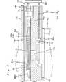
レチクルステージ装置12は、図1及びレチクルステージ装置12の斜視図である図2からわかるように、前記照明系側プレート14の下方に所定間隔を隔ててほぼ平行に配置された定盤としてのレチクルステージ定盤16、該レチクルステージ定盤16と照明系側プレート14との間に配置されたスライダとしてのレチクルステージRST、該レチクルステージRSTを取り囲む状態でレチクルステージ定盤16と照明系側プレート14との間に配置された枠状部材(重量部)18、及びレチクルステージRSTを駆動するレチクルステージ駆動系等を備えている。 As can be seen from FIG. 1 and FIG. 2 which is a perspective view of the
レチクルステージ定盤16は、不図示の支持部材によって略水平に支持されている。このレチクルステージ定盤16は、図2の分解斜視図である図3に示されるように、概略板状の部材から成り、そのほぼ中央には、突部16aが形成されている。この突部16aのほぼ中央には、照明光ILを通過させるためのX軸方向を長手方向とする矩形開口16bが、突部16aの上面とレチクルステージ定盤16の下面とを連通する状態で形成されている。レチクルステージ定盤16の下面側には、図1に示されるように、矩形開口16bの周囲を取り囲む状態で、Vリング又は伸縮自在のベローズなどのシール部材98を介して投影光学系ユニットPLの鏡筒部の上端が接続されている。 The reticle
前記レチクルステージRSTは、図4(A)に示されるような特殊な形状のレチクルステージ本体22及び該レチクルステージ本体22に固定された各種磁極ユニット(これについては後述する)等を備えている。 The reticle stage RST includes a reticle stage
レチクルステージ本体22は、平面視(上方から見て)概略矩形の板状部24Aと、該板状部24Aの−X端部に設けられたミラー部24Bと、板状部24AのY軸方向の一側及び他側の端部からそれぞれY軸方向に突設された各一対の延設部24C1,24C2,24D1,24D2とを備えている。The reticle stage
前記板状部24Aのほぼ中央部には、照明光ILの通路となる開口がその中央(内部底面)に形成された段付き開口22aが形成されている。該段付き開口22aの段部(1段掘り下げられた部分)には、レチクルRを下側から複数点(例えば3点)で支持する複数(例えば3つ)のレチクル支持部材34が設けられている。 A stepped
本実施形態では、レチクルRは、そのパターン面(下面)が、レチクルステージ本体22(レチクルステージRST)の中立面CTに略一致する状態で、複数の支持部材34によって支持されるようになっている。すなわち、レチクルRの載置面(載置部)は、レチクルステージRSTの中立面CTにほぼ一致している(図4(B)参照)。 In the present embodiment, the reticle R is supported by the plurality of
また、各レチクル支持部材34にそれぞれ対応して、板状部24Aのレチクル支持部材34近傍部分には、複数(例えば3つ)のレチクル固定機構36が設けられている。各レチクル固定機構36は、XZ断面がL字状の形状を有し、L字の角部に設けられた軸(Y軸方向の回転軸)を中心として回動自在に板状部24Aに取り付けられた固定部材を、それぞれ備えている。各固定部材は、レチクルRがレチクル支持部材34上に載置された際に、図1のステージ制御系90によって駆動される不図示の駆動機構を介して、それぞれ所定方向に回転駆動されることで、レチクル支持部材34との間でレチクルRを狭持することにより、レチクルRを機械的に固定する。この場合、固定部材が、レチクルRを支持部材34側に押圧する方向に、不図示の付勢手段によって常時付勢される構成を採用しても良い。 A plurality of (for example, three)
なお、レチクル支持部材34及びレチクル固定機構36に代えて、あるいはこれとともに、バキュームチャックや静電チャックなどの各種チャックを用いることは可能である。 Various chucks such as a vacuum chuck and an electrostatic chuck can be used in place of or together with the
前記ミラー部24Bは、図4(A)及び図5(A)を総合すると分かるように、Y軸方向を長手方向とする概略角柱状の形状を有し、その中心部分には軽量化を図るための断面円形の空洞部CH(図4(A)参照)が形成された棒状部分124aと、該棒状部分124aの長手方向の両端部を除く部分の+X側に一体的に形成された中実の補強部124bとを有している。棒状部分124aの−X側の端面は鏡面加工が施された反射面(反射部材)124mとされている。 As can be understood from FIGS. 4A and 5A, the
ミラー部24Bと板状部24Aとの間は、図5(A)に示されるヒンジ部124c,124dにより2箇所で局所的に連結されている。なお、実際には、板状部24Aとミラー部24B、ヒンジ部124c,124dを含むレチクルステージ本体部22は、一体成形(例えば、一つの部材を削り出すことにより成形)されているが、以下の説明では、説明を分かり易くするため、必要に応じて各部が別部材であるかのような表現をも用いるものとする。勿論、上記各部のいずれか1つを他と別部材で構成しても良いし、全てを別部材で構成しても良い。 The
これを更に詳述すると、図5(A)に示されるように、ミラー部24Bは、板状部24Aの−X側端部に、補強部124bの±Y側面の2箇所に設けられたヒンジ部124c,124d、すなわち回転支点を介して、連結されている。この場合、2つのヒンジ部124c,124dを結ぶ線CSが、ミラー部24Bの水平面内の曲げに際しての中立面となる。 More specifically, as shown in FIG. 5 (A), the
これにより、何らかの要因によりミラー部24Bに曲げ応力が生じた場合、図5(B)に示されるように、両ヒンジ部124c,124dの外側の範囲(A及びA’)部分のみに曲げ変形(撓み)が生じ、露光中に実際に計測に用いられる範囲(範囲B)については、曲げ変形をほぼ確実に抑制することが可能となっている。 As a result, when bending stress is generated in the
本実施形態では、さらに、図5(A)に示されるように、2箇所のヒンジ部124c,124dのうちの一方のヒンジ部124cから+X方向に所定距離だけ離れた位置に同様のヒンジ部124eが設けられている。これにより、図5(B)に示されるように、板状部24AにY軸方向への伸び(ΔL)が生じた場合であっても、ヒンジ部124cとヒンジ部124eとの間の部分124fが、ヒンジ部124cを中心として回転するような部分的な変形が生じるので、ミラー部24Bの反射面124mに対して板状部24Aの変形が与える影響が極力抑制されるようになっている。すなわち、ヒンジ部124c,124eに挟まれた部分124fは、一種のフレクシャとしての機能を有している。 In the present embodiment, as shown in FIG. 5A, the same hinge portion 124e is located at a position away from one hinge portion 124c of the two
レチクルステージ本体22の板状部24Aの−Y側端部には、図4(A)に示されるように、2つの凹部24g1,24g2が形成され、該凹部24g1,24g2のそれぞれには、レトロリフレクタ321,322がそれぞれ設けられている。As shown in FIG. 4A, two concave portions 24g1 and 24g2 are formed at the −Y side end of the plate-
前記4つの延設部24C1,24C2,24D1,24D2は、図4(A)に示されるように、概略板状の形状を有し、各延設部には強度向上のための断面三角形状の補強部が設けられている。レチクルステージ本体22の底面には、延設部24C1から延設部24D1に至るY軸方向の全域に渡る第1の気体静圧軸受が形成され、延設部24C2から延設部24D2に至るY軸方向の全域に渡る第2の気体静圧軸受が形成されている。As shown in FIG. 4A, the four extending portions 24C1 , 24C2 , 24D1 , and 24D2 have a substantially plate shape, and each extending portion has a structure for improving strength. A reinforcing portion having a triangular cross section is provided. The bottom surface of the reticle stage
次に、第1の気体静圧軸受及び第2の気体静圧軸受について図6(A)及び図6(B)に基づいて説明する。 Next, the first gas static pressure bearing and the second gas static pressure bearing will be described with reference to FIGS. 6 (A) and 6 (B).
図6(A)には、レチクルステージ本体22を下面側から見た平面図(底面図)が示されている。この図6(A)から分かるように、延設部24C1,24D1及びその間の部分を含むレチクルステージ本体22の底面には、3つの溝が形成されている。これらの溝のうちX軸方向の中央に位置する溝は、Y軸方向に延びる幹溝55Aと、該幹溝55AのX軸方向両側に連通状態とされ、かつY軸方向に所定間隔で形成されたT字状の複数の表面絞り溝55Bと、から構成される給気溝56とされている。幹溝55Aと表面絞り溝55Bとは、図6(A)のD―D線断面図である図6(B)に示されるように、幹溝55Aの方が表面絞り溝55Bよりも深く形成されている。FIG. 6A shows a plan view (bottom view) of the reticle stage
一方、前記3つの溝のうちの残りの2つの溝は、Y軸方向に延びる排気溝57A,57Bとされている。これら排気溝57A,57Bは、前記幹溝55Aとほぼ同一の断面形状を有している。 On the other hand, the remaining two of the three grooves are
一方、図6(B)(及び図3)に示されるように、これら3つの溝56、57A,57Bそれぞれの少なくとも一部に対向してレチクルステージ定盤16には、凸部16aの上面に、3つの開口(58,59A,59B)がそれぞれ形成されている。これら3つの開口のうち中央に位置する開口が給気口58とされ、両端に位置する開口が排気口59A,59Bとされている。給気口58は、図6(B)に示される給気管路60を介して不図示の気体供給装置に接続されている。気体供給装置からは例えばヘリウムなどの希ガス又は窒素等の低吸収性ガスが供給される。また、排気口59A,59Bは、排気管路61A,61Bを介して不図示の真空ポンプに接続されている。 On the other hand, as shown in FIG. 6B (and FIG. 3), the reticle
本実施形態では、不図示の気体供給装置から給気管路60を介して低吸収性ガスが供給されると、この低吸収性ガスは、図6(B)に示されるように、給気口58から給気溝56の幹溝55Aに供給され、該幹溝55AのY方向全域に行き渡る。低吸収性ガスが更に供給され続けると、給気溝56の複数の表面絞り溝55Bから低吸収性ガスがレチクルステージ定盤16の上面に噴き付けられる。 In the present embodiment, when low-absorbing gas is supplied from a gas supply device (not shown) through the
このとき、真空ポンプにより排気管路61A,61Bを介して吸引動作が行われていると、レチクルステージRSTとレチクルステージ定盤16との間の気体が排気口59A,59Bを介して外部に排気される。このため、左右の表面絞り溝55Bから排気溝57A,57Bへ向かう低吸収性ガスの流れが、レチクルステージRSTとレチクルステージ定盤16との間の隙間に生じ、一定の流速、圧力の低吸収性ガスを常時流し続けることにより、前記隙間内の加圧ガスの静圧(いわゆる隙間内圧力)が一定となって、レチクルステージRSTとレチクルステージ定盤16との間に例えば数μm程度のクリアランスが形成され、維持される。すなわち、本実施形態では、給気溝56、排気溝57A,57B、給気口58、給気管路60、排気口59A,59B、排気管路61A,61Bが形成されたレチクルステージ本体22底面の部分によって、不図示の気体供給装置からの加圧気体が、レチクルステージ定盤16から配管を介さないで供給される第1の差動排気型の気体静圧軸受が実質的に構成されている。 At this time, if the suction operation is performed by the vacuum pump through the
延設部24C2,24D2及びその間の部分を含むレチクルステージ本体22の底面にも、前述した幹溝55A及び複数の表面絞り溝55Bから構成される給気溝56と、その両側の排気溝57A、57Bとが形成され、これら3つの溝を含んで前述と同様にして、不図示の気体供給装置からの加圧気体が、レチクルステージ定盤16から配管を介さないで供給される第2の差動排気型の気体静圧軸受が実質的に構成されている。Also on the bottom surface of the reticle stage
このように、本実施形態では、第1、第2の差動排気型の気体静圧軸受の表面絞り溝55Bからレチクルステージ定盤16の上面を介して噴き付けられる加圧気体の静圧と、レチクルステージRST全体の自重とのバランスにより、レチクルステージ定盤16の上面の上方に数ミクロン程度のクリアランスを介して、レチクルステージRSTが非接触で浮上支持されるようになっている。 Thus, in the present embodiment, the static pressure of the pressurized gas sprayed from the
図2に戻り、前記枠状部材18の上面には、概略環状の凹溝(環状凹溝)83,85が二重に形成されている。このうちの内側の環状凹溝83には、その内部に複数の給気口(不図示)が形成され、外側の環状凹溝85には、複数の排気口(不図示)が形成されている。なお、以下においては内側の環状凹溝83を「給気溝83」、外側の環状凹溝85を「排気溝85」と呼ぶものとする。 Returning to FIG. 2, approximately circular concave grooves (annular concave grooves) 83 and 85 are formed on the upper surface of the frame-shaped
給気溝83の内部に形成された給気口は、不図示の給気管路及び給気管を介して窒素又は希ガスなどの低吸収性ガスを供給する不図示のガス供給装置に接続されている。また、排気溝85の内部に形成された排気口は、不図示の排気管路及び排気管を介して不図示の真空ポンプに接続されている。 An air supply port formed inside the
また、この枠状部材18の底面には、該枠状部材18を上下反転して斜視図にて示す図9から分かるように、概略環状の凹溝(環状凹溝)82,84が二重に形成されている。このうちの内側の環状凹溝82には、その内部に複数の給気口(不図示)が形成され、外側の環状凹溝84には、複数の排気口(不図示)が形成されている。なお、以下においては内側の環状凹溝82を「給気溝82」、外側の環状凹溝84を「排気溝84」と呼ぶものとする。 Further, on the bottom surface of the frame-shaped
給気溝82の内部に形成された給気口は、給気管路及び給気管を介して窒素又は希ガスなどの低吸収性ガスを供給する不図示のガス供給装置に接続されている。また、排気溝84の内部に形成された排気口は、排気管路及び排気管を介して不図示の真空ポンプに接続されている。 An air supply port formed inside the
従って、ガス供給装置と真空ポンプとが作動状態にあるときは、枠状部材18の底面に形成された給気溝82からレチクルステージ定盤16の上面に加圧気体(低吸収性ガス)が噴き付けられ、この噴き付けられた加圧気体の静圧により枠状部材18の自重が支えられ、枠状部材18がレチクルステージ定盤16の上面の上方に数μm程度のクリアランスを介して浮上支持される。この場合も、そのクリアランス内のガスは、排気溝84を介して真空ポンプの吸引力により外部に排気される。この場合、給気溝82から排気溝84に向かうガスの流れが生じている。このため、そのクリアランスを介して枠状部材18の内部に外気が混入するのが効果的に阻止されている。 Therefore, when the gas supply device and the vacuum pump are in an operating state, pressurized gas (low absorption gas) is supplied from the
このように、枠状部材18の底面の全体により、実質的に、レチクルステージ定盤16の上面の上方に枠状部材18を浮上支持する差動排気型の気体静圧軸受が構成されている。 As described above, the entire bottom surface of the frame-shaped
また、ガス供給装置と真空ポンプとが作動状態にあるときは、枠状部材18の上面に形成された給気溝83から照明系側プレート14の下面に加圧気体(低吸収性ガス)が噴き付けられるとともに、照明系側プレート14と枠状部材18との間のクリアランス内のガスは、排気溝85を介して真空ポンプの吸引力により外部に排気される。この場合、給気溝83から排気溝85に向かうガスの流れが生じている。このため、そのクリアランスを介して枠状部材18の内部に外気が混入するのが効果的に阻止されている。また、この場合、噴き付けられた加圧気体の静圧と真空吸引力とのバランスによって、枠状部材18と照明系側プレート14との間にクリアランスが維持される。すなわち、枠状部材18の上面の全体により、実質的に、枠状部材18と照明系側プレート14との間のクリアランスを維持する差動排気型の気体静圧軸受が構成されている。 Further, when the gas supply device and the vacuum pump are in an operating state, pressurized gas (low absorption gas) is supplied from the
また、本実施形態の場合、枠状部材18とレチクルステージ定盤16との間の前述のクリアランス(すなわち軸受隙間)は、枠状部材18上下の差動排気型の気体静圧軸受が枠状部材18に及ぼす力、枠状部材18全体の自重との総合的なバランスによって、実際には決定される。 In the case of the present embodiment, the above-described clearance between the frame-shaped
このように、枠状部材18と照明系側プレート14との間のクリアランス、及びレチクルステージ定盤16と枠状部材18との間のクリアランスが前述のガスの流れによって気密化され、更に、前述したように、投影光学系ユニットPLの上端部とレチクルステージ定盤16との間が前述のシール部材98により接続されているので(図7,図8参照)、枠状部材18により囲まれた空間内は非常に気密度が高い空間となっている。以下、枠状部材18により囲まれた空間を、便宜上「気密空間」と呼ぶものとする。 As described above, the clearance between the frame-shaped
本実施形態のように、真空紫外域の露光波長を使用する露光装置では、酸素等の吸収性ガスによる露光光の吸収を避けるために、照明ユニットIOPから投影光学系ユニットPLまでの光路、すなわち前述の気密空間内(の光路)についても窒素や希ガスで置換する必要がある。 As in this embodiment, in an exposure apparatus that uses an exposure wavelength in the vacuum ultraviolet region, in order to avoid exposure light absorption by an absorbing gas such as oxygen, the optical path from the illumination unit IOP to the projection optical system unit PL, that is, It is necessary to substitute nitrogen or a rare gas in the above-mentioned airtight space (the optical path).
この場合、枠状部材18の側壁に給気管、排気管をそれぞれ接続し、給気管を介して前述の気密空間に低吸収性ガスを供給し、排気管を介して内部のガスを外部に排気することとすれば良い。 In this case, an air supply pipe and an exhaust pipe are respectively connected to the side wall of the frame-
この他、枠状部材18に接続された不図示の給気管内を流れる窒素又は希ガスの一部を、枠状部材18内で給気管路の一部から分岐された給気枝管を介して上記気密空間内に流入させることによって気密空間内に窒素又は希ガスが供給され、その一方で、排気管路の一部から分岐された排気枝管を介して、気密空間内のガスが排気されるような構成を採用しても良い。このようにすれば、上記気密化に併せて、レチクルRが保持された空間内を露光光の吸収の少ない窒素又は希ガス等により置換することが可能となる。 In addition, a part of nitrogen or rare gas flowing in a supply pipe (not shown) connected to the frame-shaped
なお、気密空間に供給されるガスとしてヘリウムガスを用いる場合には、ガス排気機構を介してヘリウムガスを回収した後、不純物を除去後、再利用することが望ましい。 When helium gas is used as the gas supplied to the hermetic space, it is desirable to recover the helium gas through a gas exhaust mechanism, and then reuse it after removing impurities.
前記レチクルステージ駆動系は、図2に示されるように、枠状部材18の内部に、Y軸方向にそれぞれ架設された一対の固定子ユニット(一対の固定子部)36、38を含んで構成され、レチクルステージRSTをY軸方向に駆動するとともにθz方向(Z軸回りの回転方向)に微小駆動する第1駆動機構と、枠状部材18の内部の一方の固定子ユニット38の+X側にY軸方向に架設された固定子ユニット40を含んで構成され、レチクルステージRSTをX軸方向に微小駆動する第2駆動機構と、を備えている。 As shown in FIG. 2, the reticle stage drive system includes a pair of stator units (a pair of stator portions) 36 and 38 installed in the Y-axis direction inside the frame-shaped
前記一方の固定子ユニット36は、レチクルステージ装置12の分解斜視図である図3に示されるように、Y軸方向を長手方向とする電機子ユニットから成る一対の第1固定子としてのY軸リニアガイド1361,1362と、これらのY軸リニアガイド1361,1362をY軸方向(長手方向)の一端部と他端部で保持する一対の固定部材(保持部)152とを備えている。この場合、一対の固定部材152により、Y軸リニアガイド1361,1362は、Z軸方向(上下方向)に所定間隔をあけて相互に対向してかつXY面にそれぞれ平行に保持されている。一対の固定部材152のそれぞれは、前述の枠状部材18のY軸方向一側と他側の内壁面(側壁の内面)に固定されている。As shown in FIG. 3 which is an exploded perspective view of the
前記Y軸リニアガイド1361,1362は、図3及びレチクルステージ装置のXZ断面図を示す図7からも分かるように、断面矩形(長方形)の非磁性材料から成るフレームを有し、その内部には、Y軸方向に所定間隔で複数の電機子コイルが配設されている。The Y-axis linear guides 1361 , 1362 have a frame made of a non-magnetic material having a rectangular cross section (rectangular shape) as shown in FIG. 3 and FIG. 7 showing an XZ cross sectional view of the reticle stage device. Are provided with a plurality of armature coils at predetermined intervals in the Y-axis direction.
前記他方の固定子ユニット38も上記一方の固定子ユニット36と同様に構成されている。すなわち、固定子ユニット38は、Y軸方向を長手方向とする上下一対の電機子ユニットから成る第1固定子としてのY軸リニアガイド1381,1382と、これらのY軸リニアガイド1381,1382をZ軸方向に所定間隔を維持した状態で両端部にて固定する一対の固定部材(保持部)154とを備えている。一対の固定部材154のそれぞれは、前述の枠状部材18のY軸方向一側と他側の内壁面に固定されている。The
前記Y軸リニアガイド1381,1382は、前述のY軸リニアガイド1361,1362と同様に構成されている(図7参照)。The Y-axis linear guides 1381 and 1382 are configured in the same manner as the Y-axis linear guides 1361 and 1362 described above (see FIG. 7).
Y軸リニアガイド1361,1381と、Y軸リニアガイド1362,1382との間には、図7に示されるように、それぞれ所定のクリアランスを介して、レチクルステージRSTが配設されている。Y軸リニアガイド1361,1362にそれぞれ対向して、レチクルステージRSTの上面、下面には、一対の第1可動子としての磁極ユニット261,262がそれぞれ埋め込まれ、Y軸リニアガイド1381,1382に対向して、レチクルステージRSTの上面、下面には、一対の第1可動子としての磁極ユニット281,282がそれぞれ埋め込まれている。As shown in FIG. 7, reticle stage RST is arranged between Y-axis linear guides 1361 , 1381 and Y-axis linear guides 1362 , 1382 via predetermined clearances, respectively. Yes. Opposite to the Y-axis linear guides 1361 and 1362 , magnetic pole units 261 and 262 as a pair of first movers are embedded in the upper and lower surfaces of the reticle stage RST, respectively. Opposite to1 and 1382 , magnetic pole units 281 and 282 as a pair of first movers are embedded in the upper and lower surfaces of reticle stage RST, respectively.
磁極ユニット261,262のそれぞれは、図4(B)に示されるように、前述のレチクルステージ本体22の板状部24Aの段付き開口22aの−X側に、レチクルステージ本体22の中立面CTを基準として対称に上下面側にそれぞれ形成された凹部24e1,24e2内に配置されている。As shown in FIG. 4B, each of the magnetic pole units 261 , 262 is located in the
この場合、Y軸リニアガイド1361,1362は、上記中立面CTを基準としてほぼ対称な位置に位置している。In this case, the Y-axis linear guides 1361 and 1362 are located at substantially symmetric positions with respect to the neutral plane CT.
前記一対の磁極ユニット261,262は、磁性体部材と、該磁性体部材の表面にY軸方向に沿って所定間隔で配置された複数の界磁石とを、それぞれ備えている。複数の界磁石は、隣り合う界磁石同士で逆極性とされている。従って、磁極ユニット261の上方の空間にはY軸方向に沿って交番磁界が形成され、磁極ユニット262の下方の空間にはY軸方向に沿って交番磁界が形成されている。Each of the pair of magnetic pole units 261 and 262 includes a magnetic member and a plurality of field magnets arranged on the surface of the magnetic member at predetermined intervals along the Y-axis direction. The plurality of field magnets have opposite polarities between adjacent field magnets. Therefore, an alternating magnetic field is formed in the space above the magnetic pole unit 261 along the Y-axis direction, and an alternating magnetic field is formed in the space below the magnetic pole unit 262 along the Y-axis direction.
同様に、前記一対の磁極ユニット281,282のそれぞれは、図4(B)に示されるように、前述のレチクルステージ本体22の板状部24Aの段付き開口22aの+X側に、レチクルステージ本体22の中立面CTを基準として対称に上下面側にそれぞれ形成された凹部24f1,24f2内に配置されている。また、一対の磁極ユニット281,282は、段付き開口22aのX軸方向の中心位置(レチクルステージRSTの重心のX軸方向位置とほぼ一致)を通るZ軸に関して、磁極ユニット261,262とほぼ左右対称の配置となっている。Similarly, as shown in FIG. 4B, each of the pair of magnetic pole units 281 and 282 has a reticle on the + X side of the stepped opening 22a of the plate-
また、前記Y軸リニアガイド1381,1382は、中立面CTを基準としてほぼ対称な位置に位置している。The Y-axis linear guides 1381 and 1382 are located at substantially symmetrical positions with respect to the neutral plane CT.
前記一対の磁極ユニット281,282は、磁性体部材と、該磁性体部材の表面にY軸方向に沿って所定間隔で配置された複数の界磁石とを、それぞれ備えている。複数の界磁石は、隣り合う界磁石同士で逆極性とされている。従って、磁極ユニット281の上方の空間にはY軸方向に沿って交番磁界が形成され、磁極ユニット282の下方の空間にはY軸方向に沿って交番磁界が形成されている。Each of the pair of magnetic pole units 281 and 282 includes a magnetic member and a plurality of field magnets arranged on the surface of the magnetic member at predetermined intervals along the Y-axis direction. The plurality of field magnets have opposite polarities between adjacent field magnets. Therefore, an alternating magnetic field is formed in the space above the magnetic pole unit 281 along the Y-axis direction, and an alternating magnetic field is formed in the space below the magnetic pole unit 282 along the Y-axis direction.
本実施形態では、上述した固定子ユニット36、38(2対のY軸リニアガイド1361,1362、1381、1382を含む)と2対の磁極ユニット261、262、281、282とによって第1駆動機構が構成されている。この第1駆動機構によると、Y軸リニアガイド1361,1362内の電機子コイルに電流が供給されることにより、磁極ユニット261,262の発生する磁界と電機子ユニット1361,1362を流れる電流との間の電磁相互作用によってY軸方向の電磁力(ローレンツ力)が発生し、このローレンツ力の反力が磁極ユニット261,262(レチクルステージRST)をY軸方向に駆動する駆動力となる。In the present embodiment, the above-described
同様に、Y軸リニアガイド1381,1382内の電機子コイルに電流が供給されることにより、磁極ユニット281,282の発生する磁界とY軸リニアガイド1381,1382を流れる電流との間の電磁相互作用によってY軸方向の電磁力(ローレンツ力)が発生し、このローレンツ力の反力が磁極ユニット261,262(レチクルステージRST)をY軸方向に駆動する駆動力となる。Similarly, when a current in the Y axis linear guides 1381, 138 armature coils within2 is supplied, the magnetic pole unit 281, 282 of the generated magnetic field and the Y axis linear guides 1381, 1382 flowing current Electromagnetic force (Lorentz force) in the Y-axis direction is generated by the electromagnetic interaction between the magnetic field unit and the reaction force of the Lorentz force, and the driving force that drives the magnetic pole units 261 and 262 (reticle stage RST) in the Y-axis direction. It becomes.
本実施形態の場合、レチクルステージRSTの中立面CTを基準として、磁極ユニット261と262、磁極ユニット281と282がそれぞれ対称に配置され、これらの磁極ユニットに対応するY軸リニアガイド1361と1362、Y軸リニアガイド1381,1382も中立面CTを基準として上下対称に配置されている。このため、Y軸リニアガイド1361,1362,1381,1382の電機子コイルそれぞれに同一の電流を供給することにより、磁極ユニット261,262,281,282のそれぞれに同一の駆動力が与えられ、レチクルステージRSTの中立面CT(図4(B)参照)上の2箇所にY軸方向の駆動力(磁極ユニット261,262の駆動力の合力、磁極ユニット281,282の駆動力の合力)を作用させることができ、これにより、レチクルステージRSTにはピッチングモーメントが極力作用しないようになっている。In the present embodiment, the magnetic pole units 261 and 262 and the magnetic pole units 281 and 282 are symmetrically arranged with respect to the neutral plane CT of the reticle stage RST, and Y-axis linear corresponding to these magnetic pole units. The guides 1361 and 1362 and the Y-axis linear guides 1381 and 1382 are also arranged symmetrically with respect to the neutral plane CT. For this reason, by supplying the same current to the armature coils of the Y-axis linear guides 1361 , 1362 , 1381 , and 1382 , the same is applied to each of the magnetic pole units 261 , 262 , 281 , and 282. Drive force in the Y axis direction at two locations on the neutral plane CT of the reticle stage RST (see FIG. 4B) (the resultant force of the drive force of the magnetic pole units 261 , 262 , the magnetic pole unit). (The resultant force of the driving forces 281 and 282 ) can be applied, so that the pitching moment does not act on the reticle stage RST as much as possible.
また、この場合、磁極ユニット261と262、磁極ユニット281と282とは、X軸方向に関しても、レチクルステージRSTの重心近傍位置に関してほぼ対称に配置されているので、レチクルステージRSTの重心から等距離の2箇所に上記のY軸方向の駆動力が作用するので、該2箇所に同一の力を発生させることでレチクルステージRSTの重心位置近傍にY軸方向の駆動力の合力を作用させることが可能となっている。従って、レチクルステージRSTにはヨーイングモーメントが極力作用しないようになっている。Further, in this case, the magnetic pole units 261 and 262 and the magnetic pole units 281 and 282 are arranged substantially symmetrically with respect to the position near the center of gravity of the reticle stage RST in the X-axis direction. Since the driving force in the Y-axis direction acts at two locations that are equidistant from the center of gravity, the resultant force in the Y-axis direction is generated near the center of gravity of the reticle stage RST by generating the same force at the two locations. It is possible to act. Therefore, the yawing moment does not act on the reticle stage RST as much as possible.
なお、上記と反対に、左右のY軸方向の駆動力を異ならせることにより、レチクルステージRSTのヨーイングを制御することもできる。 Contrary to the above, yawing of reticle stage RST can be controlled by varying the driving forces in the left and right Y-axis directions.
これまでの説明から明らかなように、磁極ユニット261,262と、対応するリニアガイド1361,1362とによりレチクルステージRSTをY軸方向に駆動する一対のムービングマグネット型のY軸リニアモータが構成され、磁極ユニット281,282と、対応するY軸リニアガイド1381,1382とによりレチクルステージRSTをY軸方向に駆動する一対のムービングマグネット型のY軸リニアモータが構成されている。なお、以下においては、これらY軸リニアモータを各Y軸リニアモータを構成するリニアガイドと同一の符号を用いて、「Y軸リニアモータ1361,1362、1381,1382」とも記述するものとする。As apparent from the above description, a pair of moving magnet type Y-axis linear motors that drive the reticle stage RST in the Y-axis direction by the magnetic pole units 261 and 262 and the corresponding linear guides 1361 and 1362. A pair of moving magnet type Y-axis linear motors for driving the reticle stage RST in the Y-axis direction is configured by the magnetic pole units 281 and 282 and the corresponding Y-axis linear guides 1381 and 1382. Yes. In the following, these Y-axis linear motors are also referred to as “Y-axis linear motors 1361 , 1362 , 1381 , 1382 ” using the same reference numerals as the linear guides constituting each Y-axis linear motor. Shall.
左右各一対のY軸リニアモータ1361,1362、及び1381,1382によって、前述の第1駆動機構が構成されている。The pair of left and right Y-axis linear motors 1361 , 1362 and 1381 , 1382 constitute the first drive mechanism described above.
前記固定子ユニット40は、図3に示されるように、Y軸方向を長手方向とする一対の第2固定子としての電機子ユニット1401,1402と、これらの電機子ユニット1401,1402をY軸方向(長手方向)の一端部と他端部で保持する一対の固定部材156とを備えている。この場合、一対の固定部材156により、電機子ユニット1401,1402は、Z軸方向(上下方向)に所定間隔をあけて相互に対向してかつXY面にそれぞれ平行に保持されている。一対の固定部材156のそれぞれは、前述の枠状部材18のY軸方向一側と他側の内壁面に固定されている。As shown in FIG. 3, the
電機子ユニット1401,1402は、図7からも分かるように、断面矩形(長方形)の非磁性材料から成るフレームを有し、その内部には、電機子コイルが配置されている。As can be seen from FIG. 7, the armature units 1401 and 1402 have a frame made of a non-magnetic material having a rectangular cross section (rectangular shape), and an armature coil is disposed therein.
電機子ユニット1401,1402相互間には、図7に示されるように、それぞれ所定のクリアランスを介して、レチクルステージRSTのX軸方向の端部に固定された第2可動子としての断面矩形(長方形)の板状の永久磁石30が配置されている。永久磁石30に代えて、平板状の磁性体部材とその上下面にそれぞれ固定された一対の平板状の永久磁石とから成る磁極ユニットを用いても良い。Between the armature units 1401 and 1402 , as shown in FIG. 7, a cross section as a second mover fixed to the end of the reticle stage RST in the X-axis direction via a predetermined clearance, respectively. A rectangular (rectangular) plate-like
この場合、永久磁石30、並びに電機子ユニット1401,1402は、中立面CTを基準としてほぼ対称な形状及び配置となっている(図4(B)及び図7参照)。In this case, the
従って、永久磁石30によって形成されるZ軸方向の磁界と電機子ユニット1401,1402をそれぞれ構成する電機子コイルをY軸方向に流れる電流との間の電磁相互作用によりX軸方向の電磁力(ローレンツ力)が発生し、このローレンツ力の反力が永久磁石30(レチクルステージRST)をX軸方向に駆動する駆動力となる。Therefore, the electromagnetic force in the X-axis direction is generated by electromagnetic interaction between the magnetic field in the Z-axis direction formed by the
この場合、電機子ユニット1401,1402をそれぞれ構成する電機子コイルに同一の電流を供給することにより、レチクルステージRSTの中立面CT(図4(B)参照)上の位置にX軸方向の駆動力を作用させることができ、これにより、レチクルステージRSTにはローリングモーメントが極力作用しないようになっている。In this case, by supplying the same current to the armature coils constituting the armature units 1401 and 1402 , the X-axis is positioned on the neutral plane CT (see FIG. 4B) of the reticle stage RST. A driving force in the direction can be applied, and as a result, a rolling moment is prevented from acting on the reticle stage RST as much as possible.
上述のように、電機子ユニット1401,1402と永久磁石30とにより、レチクルステージRSTをX軸方向に微小駆動可能なムービングマグネット型のボイスコイルモータが構成されている。なお、以下においては、このボイスコイルモータを該ボイスコイルモータを構成する可動子、すなわち永久磁石の符号を用いてボイスコイルモータ30とも呼ぶものとする。このボイスコイルモータ30によって、第2駆動機構が構成されている。As described above, the armature units 1401 and 1402 and the
本実施形態では、さらに、前述の枠状部材18の+X側面及び+Y側面には、図3に示されるように、磁極ユニットから成る可動子601,602,603が設けられている。これらの可動子(第1部分)601,602,603に対応してレチクルステージ定盤16には、支持台641,642,643を介して、電機子ユニットから成る固定子(第2部分)621,622,622が設けられている。In the present embodiment, further,
前記可動子601,602は、その内部に永久磁石を備えており、Z軸方向の磁界を形成する。前記固定子621,622は、その内部に電機子コイルを有し、前記Z軸方向の磁界中を電流がY軸方向に流れるようになっている。従って、固定子621,622内の電機子コイルにY軸方向の電流が供給されることにより、可動子601,602にはX軸方向への駆動力(ローレンツ力の反力)が作用することとなる。すなわち、可動子601と固定子621とにより、ムービングマグネット型のボイスコイルモータから成るX軸方向駆動用のトリムモータが構成され、可動子602と固定子622とにより、ムービングマグネット型のボイスコイルモータから成るX軸方向駆動用のトリムモータが構成されている。The
また、前記可動子603は、その内部に永久磁石を備えており、Z軸方向の磁界を形成する。前記固定子623は、その内部に電機子コイルを有し、前記Z軸方向の磁界中を電流がX軸方向に流れるようになっている。従って、固定子623内の電機子コイルにX軸方向の電流が供給されることにより、可動子603にはY軸方向への駆動力(ローレンツ力の反力)が作用することとなる。すなわち、可動子603と固定子623とによりムービングマグネット型のボイスコイルモータから成るY軸方向駆動用のトリムモータが構成されている。Further, the
このように、これら3つのトリムモータを用いることにより、枠状部材18をX軸方向、Y軸方向、及びθz方向の3自由度方向に駆動することが可能である。 As described above, by using these three trim motors, the frame-shaped
前記枠状部材18の−X側の側壁のほぼ中央には、図3に示されるように、凹状部18aが形成されている。この凹状部18aには枠状部材18の内部と外部とを連通する矩形開口18bが形成され、該矩形開口18bには、窓ガラス(透明部)g1が嵌め込まれている。また、枠状部材18の−Y側の側壁には、枠状部材18の内部と外部とを連通する矩形開口18cが形成され、該開口18cには、窓ガラス(透明部)g2が嵌め込まれている。これらの窓ガラスg1、g2は、その取り付け部分からのガス漏れが生じないように、取り付け部分には、インジウムや銅等の金属シールや、フッ素系樹脂による封止(シーリング)が施されている。なお、上記フッ素系樹脂としては、80℃で2時間、加熱し、脱ガス処理が施されたものを使うことが望ましい。As shown in FIG. 3, a
前記窓ガラスg1の外側(−X側)には、図7から分かるように、レチクルステージRSTのミラー部24Bの反射面124mに対向して位置検出装置であるX軸レーザ干渉計69Xが設けられている。このX軸レーザ干渉計69Xからの測長ビームが窓ガラスg1を介してミラー部24Bの反射面124mに対して投射され、その反射光が窓ガラスg1を介してX軸レーザ干渉計69X内に戻る。この場合、測長ビームの光路のZ軸方向の位置は、前述の中立面CTの位置に一致している。As can be seen from FIG. 7, an
また、図7に示されるように、投影光学系ユニットPLの鏡筒の上端部近傍には、固定鏡Mrxが取付部材92を介して設けられている。X軸レーザ干渉計69Xからの参照ビームはレチクルステージ定盤16に形成された貫通孔(光路)71を介して、固定鏡Mrxに対して投射され、その反射光がX軸レーザ干渉計69X内に戻る。X軸レーザ干渉計69Xでは、測長ビームの反射光、参照ビームの反射光を内部の光学系により同軸にかつ同一の偏光方向の光に合成し、両反射光の干渉光を内部のディテクタによって受光する。そして、その干渉光によってディテクタの受光面に生じる干渉縞のカウント値に基づいて、X軸レーザ干渉計69Xは、レチクルステージ本体22のX軸方向の位置を、固定鏡Mrxを基準として、例えば0.5〜1nm程度の分解能で常時検出する。 Further, as shown in FIG. 7, a fixed mirror Mrx is provided via an
前記窓ガラスg2の外側(−Y側)には、レチクルステージ装置12近傍のYZ断面図である図8から分かるように、レチクルステージ本体22に設けられた前述のレトロリフレクタ321,322の反射面に対向して位置検出装置であるY軸レーザ干渉計69Yが設けられている。この場合、Y軸レーザ干渉計69Yは、レトロリフレクタ321,322にそれぞれ対応して一対設けられている。各Y軸レーザ干渉計69Yからの測長ビームは窓ガラスg2を介してレトロリフレクタ321、322の反射面に対してそれぞれ投射され、それぞれの反射光が窓ガラスg2を介して各Y軸レーザ干渉計69Y内に戻る。この場合、測長ビームの照射点のZ軸方向の位置は、前述の中立面CTの位置にほぼ一致している。On the outside (−Y side) of the window glass g2 , as can be seen from FIG. 8, which is a YZ sectional view in the vicinity of the
また、図8に示されるように、投影光学系ユニットPLの鏡筒の上端部近傍には、固定鏡Mryが取付部材93を介して設けられている。各Y軸レーザ干渉計69Yからの参照ビームはレチクルステージ定盤16に形成された貫通孔(光路)72をそれぞれ介して、固定鏡Mryに対してそれぞれ投射され、それぞれの反射光が各Y軸レーザ干渉計69Y内に戻る。そして、各Y軸レーザ干渉計69Yは、前述のX軸レーザ干渉計69Xと同様に、測長ビームの反射光と参照ビームの反射光との干渉光に基づいて、それぞれの測長ビームの投射位置(レトロリフレクタ321,322の反射面の位置)におけるレチクルステージ本体22のY軸方向の位置を、固定鏡Mryをそれぞれ基準として例えば0.5〜1nm程度の分解能でそれぞれ常時検出する。Further, as shown in FIG. 8, a fixed mirror Mry is provided via an
この場合、一対のY軸レーザ干渉計69Yによって、レチクルステージRSTのZ軸回りの回転量も検出することが可能となっている。 In this case, the pair of Y-
本実施形態では、図2に示されるように、ミラー部24Bは、固定子ユニット36(Y軸リニアモータ1361,1362)の外側に配置されている。このため、X軸レーザ干渉計69Xからの測長ビームがY軸リニアモータ1361,1362の固定子の上方を通過することがないことから、Y軸リニアモータ1361,1362の固定子を流れる電流による発熱により、Y軸リニアモータ1361,1362近傍に空気揺らぎが発生しても、この空気揺らぎによるX軸レーザ干渉計69Xの計測値への影響がないので、レチクルステージRST、ひいてはレチクルRのX軸方向位置を高精度で検出することが可能となる。また、この場合、前述の如く、X軸レーザ干渉計69Xの測長ビームの光路のZ軸方向の位置は、中立面CTの位置に一致しており、レチクルRの載置面も中立面CTに一致しているので、いわゆるアッベ誤差なく、レチクルステージRST、ひいてはレチクルRのX軸方向位置を精度良く計測することができる。一対のY軸干渉計69Yにおいても、同様の理由により、いわゆるアッベ誤差なく、レチクルステージRST、ひいてはレチクルRのY軸方向位置を精度良く計測することができるようになっている。In the present embodiment, as shown in FIG. 2, the
また、上述のX軸レーザ干渉計69X及び一対のY軸干渉計69Yは、枠状部材18の外部に配置されているので、各干渉計を枠状部材18の内部に配置する場合に生じる蓋然性が高い不都合の発生を防止することができる。例えば、各干渉計を構成するプリズム等の光学部材及びディテクタ等から仮に微量の吸収性ガスが発生しても、これが前述の気密空間内の低吸収性ガスに混入することがなく、結果的に露光に対して悪影響を及ぼすことがないようになっている。 Further, since the above-described
上述のように、実際には、移動鏡として、ミラー部24B、レトロリフレクタ321,322の3つが設けられ、これに対応してレーザ干渉計もX軸レーザ干渉計69Xと一対のY軸レーザ干渉計69Yとが設けられているが、図1ではこれらが代表的にレチクル移動鏡Mm、レチクル干渉計システム69として図示されている。なお、図1では、固定鏡(固定鏡Mrx、固定鏡Mry)は図示が省略されている。As described above, in practice, three
以下の説明においては、レチクル干渉計システム69によってレチクルステージRSTのXY面内の位置(θz回転を含む)が計測されているものとする。このレチクル干渉計システム69からのレチクルステージRSTの位置情報(又は速度情報)は図1のステージ制御系90及びこれを介して主制御装置70に送られ、ステージ制御系90では主制御装置70からの指示に応じ、レチクルステージRSTの位置情報(又は速度情報)に基づいてレチクルステージRSTの駆動を制御する。 In the following description, it is assumed that the position (including θz rotation) of reticle stage RST in the XY plane is measured by
図1に戻り、前記投影光学系ユニットPLとしては、両側テレセントリックな縮小系、かつ共通のZ軸方向の光軸を有する複数枚のレンズエレメントから成る屈折光学系が用いられている。この投影光学系ユニットPLは、実際には、該投影光学系ユニットPLの鏡筒部に設けられたフランジ部FLGを介して、不図示の保持部材によって保持されている。この投影光学系ユニットPLの投影倍率βは、例えば1/4あるいは1/5である。このため、前述の如く、照明ユニットIOPからの照明光ILによりレチクルRが照明されると、レチクルRに形成された前述の照明領域内の回路パターンが投影光学系ユニットPLにより照明領域と共役なウエハW上の照明光ILの照射領域(露光領域)に縮小投影され、回路パターンの縮小像(部分等立像)が転写形成される。 Returning to FIG. 1, as the projection optical system unit PL, a double-sided telecentric reduction system and a refractive optical system comprising a plurality of lens elements having a common optical axis in the Z-axis direction are used. The projection optical system unit PL is actually held by a holding member (not shown) via a flange portion FLG provided on the lens barrel portion of the projection optical system unit PL. The projection magnification β of the projection optical system unit PL is, for example, 1/4 or 1/5. Therefore, as described above, when the reticle R is illuminated by the illumination light IL from the illumination unit IOP, the circuit pattern in the illumination area formed on the reticle R is conjugate with the illumination area by the projection optical system unit PL. The projection is reduced and projected onto the irradiation area (exposure area) of the illumination light IL on the wafer W, and a reduced image (partial standing image) of the circuit pattern is transferred and formed.
投影光学系ユニットPLの鏡筒には、給気管路50の一端と、排気管路51の一端とがそれぞれ接続されている。給気管路50の他端は、不図示の低吸収性ガスの供給装置、例えばヘリウムガス供給装置に接続されている。また、排気管路51の他端は、外部のガス回収装置に接続されている。そして、ヘリウムガス供給装置から高純度のヘリウムガスが給気管路50を介して投影光学系ユニットPLの鏡筒の内部にフローされている。この場合、ヘリウムガスがガス回収装置に回収されるようになっている。なお、低吸収性ガスとしてヘリウムガスを用いているのは、前述と同様の理由に加え、投影光学系ユニットPLのレンズ材料として熱膨張係数の大きなホタル石が用いられていることから、レンズが照明光ILを吸収することにより発生する温度上昇がレンズの結像特性を劣化させることを考慮し、冷却効果の大きな低吸収性ガスであるヘリウムガスを用いることが望ましいからである。 One end of the
前記ウエハステージWSTは、ウエハ室80内に配置されている。このウエハ室80は、天井部の略中央部に円形開口71aが形成された隔壁71によって形成されている。この隔壁71は、ステンレス(SUS)等の脱ガスの少ない材料で形成されている。隔壁71の天井部の開口71a内に投影光学系ユニットPLの鏡筒の下端部が挿入されている。また、隔壁71の天井壁の開口71aの周囲と投影光学系ユニットPLのフランジ部FLGとの間は、フレキシブルベローズ97により隙間なく接続されている。このようにして、ウエハ室80の内部のガスが外部と隔離されている。 Wafer stage WST is arranged in
ウエハ室80内には、ステージベースBSが、複数の防振ユニット86を介してほぼ水平に支持されている。これらの防振ユニット86は、床面FからステージベースBSに伝達される微振動(暗振動)を例えばマイクロGレベルで絶縁する。なお、この防振ユニット86として、ステージベースBSの一部に取り付けられた半導体加速度計等の振動センサの出力に基づいてステージベースBSを積極的に制振するいわゆるアクティブ防振装置を用いることも可能である。 In the
前記ウエハステージWSTは、ウエハホルダ25を介してウエハWを真空吸着等により保持し、例えばリニアモータ等を含む不図示のウエハ駆動系によって前記ベースBSの上面に沿ってXY2次元方向に自在に駆動されるようになっている。 Wafer stage WST holds wafer W by vacuum suction or the like via
本実施形態のように、真空紫外域の露光波長を使用する露光装置では、酸素等の吸収性ガスによる露光光(照明光IL)の吸収を避けるために、投影光学系ユニットPLからウエハWまでの光路についても窒素や希ガスで置換する必要がある。 In the exposure apparatus using the exposure wavelength in the vacuum ultraviolet region as in this embodiment, from the projection optical system unit PL to the wafer W in order to avoid the absorption of the exposure light (illumination light IL) by the absorbing gas such as oxygen. It is necessary to replace the optical path with nitrogen or a rare gas.
ウエハ室80の隔壁71には、図1に示されるように、給気管路41の一端と、排気管路43の一端とがそれぞれ接続されている。給気管路41の他端は、不図示の低吸収性ガスの供給装置、例えばヘリウムガス供給装置に接続されている。また、排気管路43の他端は、外部のガス回収装置に接続されている。そして、前述と同様にして、ウエハ室80内にヘリウムガスが常時フローされている。 As shown in FIG. 1, one end of the
ウエハ室80の隔壁71の−Y側の側壁には光透過窓85が設けられている。これと同様に、図示は省略されているが、隔壁71の+X側(図1における紙面手前側)の側壁にも光透過窓が設けられている。これらの光透過窓は、隔壁71に形成された窓部(開口部)に該窓部を閉塞する光透過部材、ここでは一般的な光学ガラスを取り付けることによって構成されている。この場合、光透過窓85を構成する光透過部材の取り付け部分からのガス漏れが生じないように、取り付け部には、インジウムや銅等の金属シールや、フッ素系樹脂による封止(シーリング)が施されている。なお、上記フッ素系樹脂としては、80℃で2時間、加熱し、脱ガス処理が施されたものを使うことが望ましい。 A
前記ウエハホルダ25の−Y側の端部には、平面鏡から成るY移動鏡56YがX軸方向に延設されている。このY移動鏡56Yにほぼ垂直にウエハ室80の外部に配置されたY軸レーザ干渉計57Yからの測長ビームが光透過窓85を介して投射され、その反射光が光透過窓85を介してY軸レーザ干渉計57Y内部のディテクタによって受光され、Y軸レーザ干渉計57Y内部の参照鏡の位置を基準としてY移動鏡56Yの位置、すなわちウエハWのY位置が検出される。 At the end of the
同様に、図示は省略されているが、ウエハホルダ25の+X側の端部には、平面鏡から成るX移動鏡がY軸方向に延設されている。そして、このX移動鏡を介してX軸レーザ干渉計によって上記と同様にしてX移動鏡の位置、すなわちウエハWのX位置が検出される。上記2つのレーザ干渉計の検出値(計測値)はステージ制御系90及びこれを介して主制御装置70に供給されており、ステージ制御系90では、主制御装置70の指示に基づき、上記2つのレーザ干渉計の検出値をモニタしつつウエハ駆動系を介してウエハステージWSTの位置制御を行うようになっている。 Similarly, although not shown, an X moving mirror composed of a plane mirror extends in the Y-axis direction at the end of the
このように、本実施形態では、レーザ干渉計、すなわちレーザ光源、プリズム等の光学部材及びディテクタ等が、ウエハ室80の外部に配置されているので、上記ディテクタ等から仮に微量の吸収性ガスが発生しても、これが露光に対して悪影響を及ぼすことがないようになっている。 As described above, in this embodiment, since the laser interferometer, that is, the optical member such as the laser light source and the prism, and the detector are disposed outside the
なお、前述した投影光学系ユニットPLの鏡筒に接続された給気管路50の他端、及び排気管路51の他端を不図示のヘリウムガス供給装置にそれぞれ接続し、ヘリウムガス供給装置から給気管路50を介して常時高純度のヘリウムガスを投影光学系ユニットPLの鏡筒内に供給し、該鏡筒内部のガスを排気管路51を介してヘリウムガス供給装置に戻し、このようにして、ヘリウムガスを循環使用する構成を採用しても良い。この場合、ヘリウムガス供給装置には、ガス精製装置を内蔵することが望ましい。このようにすると、ガス精製装置の作用により、ヘリウムガス供給装置と投影光学系ユニットPL内部とを含む循環経路によりヘリウムガスを長時間に渡って循環使用しても、投影光学系ユニットPL内のヘリウムガス以外の吸収性ガス(酸素、水蒸気、有機物等)の濃度は数ppm以下の濃度に維持できる。また、この場合、投影光学系ユニットPL内に圧力センサ、吸収性ガス濃度センサ等のセンサを設け、該センサの計測値に基づいて、不図示の制御装置を介してヘリウムガス供給装置に内蔵されたポンプの作動、停止を適宜制御することとしても良い。 The other end of the
同様に、ウエハ室80にも、上記と同様のヘリウムガスの循環経路を採用しても良い。 Similarly, the same helium gas circulation path as described above may be adopted for the
次に、上述のようにして構成された露光装置10による露光動作の流れについて簡単に説明する。 Next, the flow of the exposure operation by the
まず、主制御装置70の管理の下、不図示のレチクルローダ、ウエハローダによって、レチクルロード、ウエハロードが行なわれ、また、レチクルアライメント系、ウエハステージWST上の基準マーク板、オフアクシス・アライメント検出系(いずれも図示省略)等を用いて、レチクルアライメント、アライメント検出系のベースライン計測(アライメント検出系の検出中心から投影光学系ユニットPLの光軸距離の計測)等の準備作業が所定の手順で行なわれる。 First, under the control of the
その後、主制御装置70により、不図示のアライメント検出系を用いてEGA(エンハンスト・グローバル・アライメント)等のアライメント計測が実行される。このような動作においてウエハWの移動が必要な場合には、主制御装置70からの指示に基づき、ステージ制御系90が不図示のウエハ駆動系を介して、ウエハWを保持するウエハステージWSTを所定の方向に移動させる。 Thereafter, alignment measurement such as EGA (Enhanced Global Alignment) is performed by
なお、上記のレチクルアライメント、ベースライン計測等については、例えば特開平7−176468号公報及びこれに対応する米国特許第5,646,413号に詳細に開示され、また、EGAについては、特開昭61−44429号公報及びこれに対応する米国特許第4,780,617号等に詳細に開示されている。The above reticle alignment, baseline measurement, etc. are disclosed in detail in, for example, Japanese Patent Application Laid-Open No. 7-176468 and US Pat. No. 5,646,413 corresponding thereto. No. 61-44429 and U.S. Pat. No. 4,780,617 corresponding thereto are disclosed in detail.
上記のEGA(アライメント計測)の終了後、以下のようにしてステップ・アンド・スキャン方式の露光動作が行なわれる。 After the EGA (alignment measurement) is completed, a step-and-scan exposure operation is performed as follows.
この露光動作にあたって、まず、ウエハWのXY位置が、ウエハW上の最初のショット領域(ファースト・ショット)の露光のための走査開始位置(加速開始位置)となるように、ウエハステージWSTが移動される。同時に、レチクルRの位置が走査開始位置となるように、レチクルステージRSTが移動される。そして、主制御装置70からの指示により、ステージ制御系90がレチクル干渉計システム69によって計測されたレチクルRの位置情報、及びウエハ側のY軸レーザ干渉計57Y及びX軸レーザ干渉計によって計測されたウエハWの位置情報に基づき、レチクルR(レチクルステージRST)とウエハW(ウエハステージWST)とを同期移動させることにより、走査露光が行なわれる。 In this exposure operation, first, wafer stage WST is moved so that the XY position of wafer W becomes a scanning start position (acceleration start position) for exposure of the first shot area (first shot) on wafer W. Is done. At the same time, the reticle stage RST is moved so that the position of the reticle R becomes the scanning start position. Then, in accordance with an instruction from the
このようにして、最初のショット領域に対するレチクルパターンの転写が終了すると、ウエハステージWSTが非走査方向(X軸方向)に1ショット領域分だけステッピングされた後、次のショット領域に対する走査露光が行なわれる。このようにして、ショット間ステッピング動作と走査露光とが順次繰り返され、ウエハW上に複数のショット領域にレチクルRのパターンが転写される。 When the transfer of the reticle pattern to the first shot area is thus completed, wafer stage WST is stepped by one shot area in the non-scanning direction (X-axis direction), and then scanning exposure is performed on the next shot area. It is. In this way, the stepping operation between shots and the scanning exposure are sequentially repeated, and the pattern of the reticle R is transferred onto the wafer W to a plurality of shot areas.
上記の走査露光に際して、主制御装置70の指示に基づき、ステージ制御系90によりウエハステージWSTに対するレチクルステージRSTの追従制御が行われるが、この際にレチクルステージRSTの移動に伴う反力が、上記枠状部材18の移動によりキャンセルされている。以下、この点について説明する。 At the time of the above scanning exposure, the
すなわち、上記の追従制御の際に、レチクルステージRSTがX軸方向に駆動されると、前述のボイスコイルモータ30の可動子がレチクルステージRSTと一体でX軸方向に駆動され、この駆動力の反力がボイスコイルモータ30の固定子(電機子ユニット1401,1402)及び該固定子が固定された枠状部材18に作用することとなる。この場合、枠状部材18は、レチクルステージ定盤16及び照明系側プレート14に対して所定のクリアランスを介して非接触とされているので、前記反力の作用により、枠状部材18は、運動量保存の法則に従った距離だけその反力に応じた方向に移動する。この枠状部材18の移動により、前記反力が吸収される。このとき、レチクルステージRSTのY軸方向の位置によっては、上記のX軸方向に駆動力の反力に起因するヨーイングモーメントが枠状部材18に作用することがある。この場合、枠状部材18は、そのヨーイングモーメント及びX軸方向の反力の作用によって、運動量保存の法則に従って反力を吸収するようにθz回転を伴う自由運動をする。That is, when the reticle stage RST is driven in the X-axis direction during the follow-up control, the mover of the
一方、レチクルステージRSTがウエハステージWSTとの同期をとるために、Y軸方向に駆動される際には、Y軸リニアモータ1361,1362、1381,1382の各可動子がレチクルステージRSTと一体でY軸方向に駆動され、各可動子の駆動力の反力の合力がY軸リニアモータ1361,1362、1381,1382の各固定子及びこれらが固定された枠状部材18に作用する。この場合も、上記反力の合力の作用により、枠状部材18は、運動量保存の法則に従って、前記反力の合力を吸収する距離だけその反力の合力に応じた方向に移動する。On the other hand, when the reticle stage RST is driven in the Y-axis direction in order to synchronize with the wafer stage WST, the movers of the Y-axis linear motors 1361 , 1362 , 1381 , and 1382 are moved to the reticle stage. The Y-axis linear motors 1361 , 1362 , 1381 , and 1382 are driven in the Y-axis direction integrally with the RST. Acts on the
また、Y軸リニアモータ1361,1362と、Y軸リニアモータ1381,1382とが発生する駆動力(推力)を異ならせてレチクルステージRSTをθz回転させ、その際、ヨーイングモーメントが枠状部材18に作用することがあるが、かかる場合にも、枠状部材18は、そのヨーイングモーメント及びY軸方向の反力の作用によって、運動量保存の法則に従って反力を吸収するようにθz回転を伴う自由運動をする。Further, the driving force (thrust) generated by the Y-axis linear motors 1361 , 1362 and the Y-axis linear motors 1381 , 1382 is varied to rotate the reticle stage RST by θz, and the yawing moment is In this case, the frame-shaped
また、いずれの場合にも、枠状部材18及びレチクルステージRSTを含む系の重心移動は生じないので、レチクルステージ定盤16には偏荷重は作用しない。 In any case, the center of gravity of the system including the
従って、本実施形態では、レチクルステージRSTの駆動時に、該レチクルステージRSTの駆動に伴って生じる反力(X軸方向及びY軸方向の反力)及び該反力によって生じるヨーイングモーメントを確実にキャンセルすることが可能となり、レチクルステージRSTの駆動に伴う振動を抑制することが可能となる。また、上述の如く偏荷重の発生をも防止できるので、これに起因するレチクルステージ定盤16の姿勢変化なども防止できる。 Therefore, in the present embodiment, when the reticle stage RST is driven, the reaction force (reaction force in the X-axis direction and the Y-axis direction) generated by driving the reticle stage RST and the yawing moment generated by the reaction force are surely canceled. Thus, it is possible to suppress vibration associated with driving of the reticle stage RST. In addition, since the occurrence of an offset load can be prevented as described above, a change in the posture of the reticle
また、本実施形態では、上記の反力キャンセルのため、レチクルステージ定盤16上方を枠状部材18が移動する際に、その基準位置からのずれ量が許容値を超えないように(すなわち、例えば、枠状部材18の移動により、ボイスコイルモータ30の制御が不能となる、あるいは、枠状部材18とレチクルステージ定盤16との間の隙間を介して外気が枠状部材18内部の気密空間内に混入するなどの事態が発生しないように)、例えば露光に影響を与えない適宜なときに、主制御装置70がステージ制御系90を介して前述の3つのトリムモータを用いて枠状部材18を所定の基準位置に戻すようになっている。 Further, in the present embodiment, because of the above reaction force cancellation, when the frame-shaped
以上詳細に説明したように、本実施形態に係るレチクルステージ装置12によると、レチクルステージRSTが、レチクルステージ定盤16の上方に浮上しつつレチクルRを保持してY軸及びこれに直交するX軸を含む2次元面内の3自由度方向にレチクルステージ定盤16に沿って移動可能であり、枠状部材18は、レチクルステージ定盤16の上方に浮上しつつ前記2次元面内の3自由度を有している。また、枠状部材18には、Y軸リニアモータ1361,1362、1381,1382の各固定子(リニアガイド1361,1362、1381,1382)、及びボイスコイルモータ30の固定子(電機子ユニット1401,1402)が設けられ、Y軸リニアモータ1361,1362、1381,1382の各可動子(磁極ユニット261,262、281,282)、及びボイスコイルモータ30の可動子(永久磁石30)が、レチクルステージRSTに設けられている。As described above in detail, according to the
従って、レチクルステージRSTがY軸リニアモータ1361,1362、1381,1382又はボイスコイルモータ30によりY軸方向又はX軸方向に駆動されると、その駆動力に応じた反力が固定子(リニアガイド1361,1362、1381,1382)又は固定子(電機子ユニット1401,1402)に生じる(作用する)。この反力の作用により枠状部材18が、運動量保存則にほぼ従って、2次元面内の3自由度方向に移動する。すなわち、枠状部材18がカウンタマスの役目を果たす。この場合、レチクルステージRSTの移動により、前記反力がほぼ完全にキャンセルされるとともに、レチクルステージRST及び枠状部材18を含む系の重心移動が生じないので、レチクルステージ定盤16には偏荷重も作用しない。従って、レチクルRが載置されるレチクルステージRSTの位置制御性の向上を図ることができる。Accordingly, when the reticle stage RST is driven in the Y-axis direction or the X-axis direction by the Y-axis linear motors 1361 , 1362 , 1381 , 1382 or the
また、枠状部材18はレチクルステージRSTを取り囲む状態で設けられているので、必然的に大型化し、その質量が大きくなり、枠状部材18とレチクルステージRSTとの大きな質量比を確保することができるので、枠状部材18の移動ストロークは比較的短くて足りる。また、枠状部材18を大型化する場合にも、その支障は殆どない。 Further, since the frame-shaped
また、レチクルステージRSTには、中立面CTの一部にレチクルRの載置面が形成されるとともに、レチクル干渉計システム69からの測長ビームの光路のZ軸方向の位置が中立面CTの位置に一致しているので、前述の図12(B)を用いて説明した従来例と異なり、レチクルステージRSTの変形の際に中立面CTと測長軸とのずれに起因して生じる位置計測誤差、及び測長軸とレチクルRのパターン面の位置ずれに相違する一種のアッベ誤差をともに、略零にすることができ、これによりレチクルRの位置を高精度に計測することが可能となる。 In addition, on reticle stage RST, a mounting surface for reticle R is formed on part of neutral surface CT, and the position of the optical path of the measuring beam from
また、レチクルステージRSTを駆動する第1駆動機構が、レチクルステージRSTのレチクルRの載置領域のX軸方向の一側と他側とに中立面CTを基準としてそれぞれ対称に配置された各一対の可動子(磁極ユニット261,262、281,282)と、当該各可動子と個別に協働してY軸方向の駆動力をそれぞれ発生する2対の固定子(リニアガイド1361,1362、1381,1382)とを有している。すなわち、X軸方向の一側、他側のいずれにおいても、可動子、レチクルステージ本体、可動子の積層構造になっているとともに、その可動子同士は、中立面CTに関して対称の配置となっている。この場合、レチクルステージRSTの中立面は、その重心の高さ位置(Z軸方向の位置)に略一致しているので、左右各一対の可動子と対応する固定子との協働によって発生するY軸方向の駆動力の合力が、レチクルステージRSTの重心位置に作用することとなる。In addition, the first drive mechanisms that drive the reticle stage RST are arranged symmetrically on one side and the other side in the X-axis direction of the reticle R mounting area of the reticle stage RST with respect to the neutral plane CT. A pair of movers (magnetic pole units 261 , 262 , 281 , 282 ) and two pairs of stators (linear guides) that individually generate a driving force in the Y-axis direction in cooperation with the movers. 1361 , 1362 , 1381 , 1382 ). That is, on either the one side or the other side in the X-axis direction, the movable element, the reticle stage main body, and the movable element have a laminated structure, and the movable elements are arranged symmetrically with respect to the neutral plane CT. ing. In this case, the neutral plane of the reticle stage RST substantially coincides with the height position of the center of gravity (position in the Z-axis direction), and thus is generated by the cooperation of the pair of left and right movable elements and the corresponding stator. The resultant force of the driving force in the Y-axis direction acts on the position of the center of gravity of reticle stage RST.
また、前記各対の固定子(リニアガイド1361,1362、1381,1382)は、前記中立面CTを基準としてそれぞれ対称に配置されているので、レチクルステージRSTをレチクルステージ定盤16に沿ってY軸方向に駆動する際に、リニアガイド1361,1362、1381,1382それぞれの電機子コイルに供給される電流によるリニアガイド1361,1362、1381,1382の発熱により、レチクルステージRSTが加熱されたとしても、その発熱部分では、中立面CTの上側、下側に生じるバイメタル効果に起因するレチクルステージ本体22の変形同士が相殺され、結果的にバイメタル効果に起因するレチクルステージRSTの変形が生じることがない。Further, since each of the pair of stators (linear guides 1361 , 1362 , 1381 , 1382 ) is arranged symmetrically with respect to the neutral plane CT, the reticle stage RST is used as a reticle stage surface plate. When driving in the Y-axis direction along 16, the linear guides 1361 , 1362 , 1381 , 1382 by the current supplied to the armature coils of the linear guides 1361 , 1362 , 1381 , 1382 respectively. Even if the reticle stage RST is heated by the heat generation of the reticle stage, the deformation of the reticle stage
なお、本実施形態と異なり、例えば上記各一対の可動子が電機子ユニットで構成される場合には、レチクルステージRSTをレチクルステージ定盤16に沿ってY軸方向に駆動する際に、可動子に供給される電流による可動子の発熱によりスライダが加熱されるが、この場合も、同様の理由により、バイメタル効果に起因してレチクルステージRSTの変形が生じることがないようになっている。 Unlike the present embodiment, for example, when each of the pair of movers is constituted by an armature unit, the mover is moved when the reticle stage RST is driven along the reticle
従って、レチクルステージRSTのY軸方向の位置をレチクルステージRSTに設けられた一対のレトロリフレクタ321、322を介して一対のY軸干渉計69Yにより計測し、その計測結果に基づいてレチクルステージRSTのY軸方向の位置を制御するので、そのレチクルステージRSTのY軸方向の位置制御性を極めて良好にすることができる。Therefore, the position of reticle stage RST in the Y-axis direction is measured by a pair of Y-
また、本実施形態に係るレチクルステージ装置12では、レチクル干渉計システム69からのX軸方向の測長ビームが照射される反射面が、レチクルステージRSTをY軸方向に駆動するリニアモータ1361,1362よりも外側に設けられているので、そのリニアモータの発熱に起因して該リニアモータ周辺の気体に温度揺らぎが生じても、そのX軸方向の測長ビームにはなんらの影響も生じない。これにより、X軸干渉計69XによるレチクルステージRSTのX軸方向の位置計測を高精度で行うことが可能となる。この場合、レチクル干渉計システム69からのY軸方向の測長ビームは、通常と同様に、レチクルステージRSTに設けられたレトロリフレクタ321、322の反射面(前記リニアモータの発熱の影響を殆ど受けない場所に位置する反射面)に特に支障なく照射することができるので、レチクルステージRSTのY軸方向及びX軸方向の位置を精度良く計測することが可能となり、ひいてはレチクルステージRSTの位置制御性の向上を図ることが可能となる。In the
また、レチクル干渉計システム69からのX軸方向の測長ビームが照射される反射面124mは、レチクルステージRSTのレチクルRが載置される板状部24Aとは別の所定長さの棒状のミラー部24Bの端面に形成され、該ミラー部24Bの反射面124mが形成された棒状部分124aの長手方向の両端部を除く部分に補強部124bが設けられ、該補強部124bの両端が弾性ヒンジ部124c,124dを介して板状部24Aに連結されている。このため、反射面の弾性ヒンジ部124cと弾性ヒンジ部124dとの間の部分、すなわち、レチクルステージRSTの位置制御に主として用いられる部分の変形を極力抑制することができる。 Further, the
また、レチクルステージRSTのY軸方向の一側及び他側の端部にはY軸方向に延びる延設部24C1〜24D2がそれぞれ設けられ、レチクルステージRSTの底面には、前記一側の延設部から他側の延設部に至る長手方向の全域に渡る気体静圧軸受が形成され、レチクルステージ定盤16から配管を介さないで前記気体静圧軸受に対して加圧気体が供給される構成が採用されている。このため、レチクルステージRSTが配管を引きずった状態で駆動することがなく、レチクルステージが等速運動を行う露光中においては、等速運動を保つのに必要な推力をほとんど必要としないため、リニアモータの推力リップルその他の影響を受けなくなる。In addition, extending portions 24C1 to 24D2 extending in the Y-axis direction are respectively provided at one end and the other end of the reticle stage RST in the Y-axis direction, and the bottom surface of the reticle stage RST has the one side on the one side. A gas static pressure bearing is formed over the entire area in the longitudinal direction from the extending portion to the extending portion on the other side, and pressurized gas is supplied from the reticle
また、本実施形態に係る露光装置10によると、上述の如く、レチクルステージRSTの位置制御性を極めて良好に確保することができるので、レチクルステージRSTとウエハステージWSTとの同期制御精度を向上させることができ、これにより、レチクルRに形成されたパターンをウエハW上に高精度に転写することが可能となる。 Further, according to the
また、露光装置10によると、照明ユニットIOPと投影光学系ユニットPLとの間の照明光ILの光路を含む空間が低吸収性ガス(照明光ILを吸収する特性が空気に比べて小さい特定ガス)でパージされるパージ空間とされるとともに、枠状部材18が前記パージ空間を外気に対して隔離する隔壁を兼ねているので、レチクルステージRST周辺の空間を容易にパージ空間とすることができ、そのパージ空間内での照明光ILの吸収を極力抑制することができる。 Further, according to the
なお、上記実施形態では、レチクルステージRSTをY軸方向に駆動する第1駆動機構を左右各一対のY軸リニアモータで構成し、レチクルステージRSTをX軸方向に駆動する第2駆動機構をボイスコイルモータで構成するものとしたが、本発明がこれに限定されないことは勿論である。 In the above embodiment, the first drive mechanism that drives the reticle stage RST in the Y-axis direction is configured by a pair of left and right Y-axis linear motors, and the second drive mechanism that drives the reticle stage RST in the X-axis direction is a voice. Although the coil motor is used, the present invention is not limited to this.
また、上記実施形態では、ミラー部24Bには空洞部CHが形成されている場合について説明したが、ミラー部24Bに中空部を形成しなくても良い。また、ミラー部24Bと板状部24Aとを一体成形するものとして説明したが、これに限らず、これらを別部材にて構成し、各部の間を弾性ヒンジ部にて連結することとしても良い。 Moreover, although the said embodiment demonstrated the case where the cavity part CH was formed in the
なお、上記実施形態では、レチクルステージ装置12の上方に、照明系側プレート14を設けるものとしたが、例えば枠状部材の上側(照明系側)を照明光を透過する窓部を残して塞ぐことで、照明系側プレート14を設けなくともレチクルステージRST近傍をある程度気密な空間に維持することは可能である。 In the above-described embodiment, the illumination
なお、上記実施形態では、レチクルステージRSTを取り囲む枠状部材18がレチクルステージ周辺の空間を外気に対して隔離する隔壁を兼ねている場合について説明したが、本発明がこれに限られるものではなく、レチクルステージRST及び枠状部材をチャンバ(レチクルステージチャンバ)内に収納し、レチクルステージRST周辺の空間を低吸収性ガスにより置換することとしても良い。この場合、枠状部材についてはレチクルステージ定盤との間に所定間隔を形成し、2次元面内(XY面内)で移動可能に構成するのみで良く、上記実施形態のように枠状部材の上面に気体静圧軸受機構を設ける必要はない。 In the above embodiment, the case where the frame-shaped
なお、上記実施形態では,本発明に係るステージ装置が走査型のVUV露光装置のレチクルステージ装置に適用された場合について説明したが、これに限らず、本発明に係るステージ装置は,投影光学系を用いることなくマスクと基板とを密着させてマスクパターンを基板に転写するプロキシミティタイプのアライナーのマスクステージ装置や、液晶用の一括転写方式の走査型露光装置などのマスクステージ装置あるいはプレートステージ装置などに好適に適用できる。この他、EBPS方式の電子線露光装置、波長5〜30nm程度の軟X線領域の光を露光光として用いるいわゆるEUVL等の露光装置にも本発明に係るステージ装置は適用できる。 In the above-described embodiment, the case where the stage apparatus according to the present invention is applied to the reticle stage apparatus of a scanning VUV exposure apparatus has been described. However, the present invention is not limited to this, and the stage apparatus according to the present invention includes a projection optical system. Mask stage device or plate stage device such as a proximity type aligner mask stage device for transferring a mask pattern to the substrate without using a mask, and a batch transfer scanning exposure device for liquid crystal It can be suitably applied to. In addition, the stage apparatus according to the present invention can also be applied to an EBPS electron beam exposure apparatus and an exposure apparatus such as a so-called EUVL that uses light in a soft X-ray region having a wavelength of about 5 to 30 nm as exposure light.
この他、物体(試料)が載置される移動体を所定の第1軸方向に駆動可能でその第1軸方向に直交する第2軸方向及び回転方向にも微小駆動が必要な装置であれば、露光装置に限らず、その他の精密機械などにも本発明に係るステージ装置は好適に適用できる。 In addition, the moving body on which the object (sample) is placed can be driven in a predetermined first axis direction, and the apparatus needs to be finely driven in the second axis direction and the rotation direction orthogonal to the first axis direction. For example, the stage apparatus according to the present invention can be suitably applied not only to the exposure apparatus but also to other precision machines.
なお、上記実施形態では、照明光ILとしては、ArFエキシマレーザ光(波長193nm)あるいはF2レーザ光(波長157nm)などの真空紫外光、KrFエキシマレーザ光(波長248nm)などの遠紫外光、超高圧水銀ランプからの紫外域の輝線(g線、i線等)を用いるものとしたが、これに限らず、Ar2レーザ光(波長126nm)などの他の真空紫外光を用いても良い。また、例えば、真空紫外光として上記各レーザ光に限らず、DFB半導体レーザ又はファイバーレーザから発振される赤外域、又は可視域の単一波長レーザ光を、例えばエルビウム(Er)(又はエルビウムとイッテルビウム(Yb)の両方)がドープされたファイバーアンプで増幅し、非線形光学結晶を用いて紫外光に波長変換した高調波を用いても良い。さらに、照明光ILとして紫外光などでなく、X線(EUV光を含む)又は電子線やイオンビームなどの荷電粒子線などを用いても良い。In the above embodiment, as the illumination light IL, vacuum ultraviolet light such as ArF excimer laser light (wavelength 193 nm) or F2 laser light (wavelength 157 nm), far ultraviolet light such as KrF excimer laser light (
また、上記実施形態では、投影光学系ユニットPLとして縮小系を用いる場合について説明したが、投影光学系は等倍系および拡大系のいずれでも良い。また、投影光学系としては、照明光ILとして、例えばAr2レーザ光などの真空紫外光を用いる場合などには、例えば特開平3−282527号公報及びこれに対応する米国特許第5,220,454号、特開平8―171054号公報及びこれに対応する米国特許第5,668,672号、並びに特開平10−20195号公報及びこれに対応する米国特許第5,835,275号などに開示される、屈折光学素子と反射光学素子(凹面鏡やビームスプリッタ等)とを組み合わせたいわゆるカタディオプトリック系(反射屈折系)、あるいは反射光学素子のみから成る反射光学系が主として用いられる。In the above-described embodiment, the case where the reduction system is used as the projection optical system unit PL has been described. However, the projection optical system may be either a unity magnification system or an enlargement system. As the projection optical system, for example, when vacuum ultraviolet light such as Ar2 laser light is used as the illumination light IL, for example, Japanese Patent Laid-Open No. 3-282527 and US Pat. No. 5,220, corresponding thereto. No. 454, JP-A-8-171054 and the corresponding US Pat. No. 5,668,672, and JP-A-10-20195 and the corresponding US Pat. No. 5,835,275. A so-called catadioptric system (a catadioptric system) in which a refractive optical element and a reflective optical element (such as a concave mirror or a beam splitter) are combined, or a reflective optical system composed only of a reflective optical element is mainly used.
なお、上記実施形態では、本発明が半導体製造用の露光装置に適用された場合について説明したが、これに限らず、例えば、角型のガラスプレートに液晶表示素子パターンを転写する液晶用の露光装置や、薄膜磁気ヘッド、撮像素子、有機EL、マイクロマシン、DNAチップなどを製造するための露光装置などにも本発明は広く適用できる。 In the above-described embodiment, the case where the present invention is applied to an exposure apparatus for manufacturing a semiconductor has been described. However, the present invention is not limited to this, and for example, exposure for liquid crystal that transfers a liquid crystal display element pattern onto a square glass plate. The present invention can be widely applied to an apparatus, an exposure apparatus for manufacturing a thin film magnetic head, an image sensor, an organic EL, a micromachine, a DNA chip, and the like.
また、半導体素子などのマイクロデバイスだけでなく、光露光装置、EUV露光装置、X線露光装置、及び電子線露光装置などで使用されるレチクル又はマスクを製造するために、ガラス基板又はシリコンウエハなどに回路パターンを転写する露光装置にも本発明を適用できる。ここで、DUV(遠紫外)光やVUV(真空紫外)光などを用いる露光装置では一般的に透過型レチクルが用いられ、レチクル基板としては石英ガラス、フッ素がドープされた石英ガラス、螢石、フッ化マグネシウム、又は水晶などが用いられる。 Further, in order to manufacture reticles or masks used in not only microdevices such as semiconductor elements but also light exposure apparatuses, EUV exposure apparatuses, X-ray exposure apparatuses, and electron beam exposure apparatuses, glass substrates, silicon wafers, etc. The present invention can also be applied to an exposure apparatus that transfers a circuit pattern. Here, in an exposure apparatus using DUV (far ultraviolet) light, VUV (vacuum ultraviolet) light, or the like, a transmission type reticle is generally used. As a reticle substrate, quartz glass, fluorine-doped quartz glass, meteorite, Magnesium fluoride or quartz is used.
なお、例えば国際公開第99/49504号などに開示される、投影光学系ユニットPLとウエハとの間に液体が満たされる液浸露光装置に本発明を適用しても良い。
《デバイス製造方法》
次に、上述した露光装置をリソグラフィ工程で使用したデバイスの製造方法の実施形態について説明する。For example, the present invention may be applied to an immersion exposure apparatus disclosed in International Publication No. 99/49504 or the like in which a liquid is filled between the projection optical system unit PL and the wafer.
<Device manufacturing method>
Next, an embodiment of a device manufacturing method using the above-described exposure apparatus in a lithography process will be described.
図10には、デバイス(ICやLSI等の半導体チップ、液晶パネル、CCD、薄膜磁気ヘッド、マイクロマシン等)の製造例のフローチャートが示されている。図10に示されるように、まず、ステップ201(設計ステップ)において、デバイスの機能・性能設計(例えば、半導体デバイスの回路設計等)を行い、その機能を実現するためのパターン設計を行う。引き続き、ステップ202(マスク製作ステップ)において、設計した回路パターンを形成したマスクを製作する。一方、ステップ203(ウエハ製造ステップ)において、シリコン等の材料を用いてウエハを製造する。 FIG. 10 shows a flowchart of a manufacturing example of a device (a semiconductor chip such as an IC or LSI, a liquid crystal panel, a CCD, a thin film magnetic head, a micromachine, etc.). As shown in FIG. 10, first, in step 201 (design step), device function / performance design (for example, circuit design of a semiconductor device) is performed, and pattern design for realizing the function is performed. Subsequently, in step 202 (mask manufacturing step), a mask on which the designed circuit pattern is formed is manufactured. On the other hand, in step 203 (wafer manufacturing step), a wafer is manufactured using a material such as silicon.
次に、ステップ204(ウエハ処理ステップ)において、ステップ201〜ステップ203で用意したマスクとウエハを使用して、後述するように、リソグラフィ技術等によってウエハ上に実際の回路等を形成する。次いで、ステップ205(デバイス組立ステップ)において、ステップ204で処理されたウエハを用いてデバイス組立を行う。このステップ205には、ダイシング工程、ボンディング工程、及びパッケージング工程(チップ封入)等の工程が必要に応じて含まれる。 Next, in step 204 (wafer processing step), using the mask and wafer prepared in
最後に、ステップ206(検査ステップ)において、ステップ205で作製されたデバイスの動作確認テスト、耐久性テスト等の検査を行う。こうした工程を経た後にデバイスが完成し、これが出荷される。 Finally, in step 206 (inspection step), inspections such as an operation confirmation test and a durability test of the device manufactured in
図11には、半導体デバイスの場合における、上記ステップ204の詳細なフロー例が示されている。図11において、ステップ211(酸化ステップ)においてはウエハの表面を酸化させる。ステップ212(CVDステップ)においてはウエハ表面に絶縁膜を形成する。ステップ213(電極形成ステップ)においてはウエハ上に電極を蒸着によって形成する。ステップ214(イオン打込みステップ)においてはウエハにイオンを打ち込む。以上のステップ211〜ステップ214それぞれは、ウエハ処理の各段階の前処理工程を構成しており、各段階において必要な処理に応じて選択されて実行される。 FIG. 11 shows a detailed flow example of
ウエハプロセスの各段階において、上述の前処理工程が終了すると、以下のようにして後処理工程が実行される。この後処理工程では、まず、ステップ215(レジスト形成ステップ)において、ウエハに感光剤を塗布する。引き続き、ステップ216(露光ステップ)において、上記実施形態の露光装置10その他の本発明の露光装置によってマスクの回路パターンをウエハに転写する。次に、ステップ217(現像ステップ)においては露光されたウエハを現像し、ステップ218(エッチングステップ)において、レジストが残存している部分以外の部分の露出部材をエッチングにより取り去る。そして、ステップ219(レジスト除去ステップ)において、エッチングが済んで不要となったレジストを取り除く。 At each stage of the wafer process, when the above pre-process is completed, the post-process is executed as follows. In this post-processing process, first, in step 215 (resist formation step), a photosensitive agent is applied to the wafer. Subsequently, in step 216 (exposure step), the circuit pattern of the mask is transferred to the wafer by the
これらの前処理工程と後処理工程とを繰り返し行うことによって、ウエハ上に多重に回路パターンが形成される。 By repeatedly performing these pre-processing steps and post-processing steps, multiple circuit patterns are formed on the wafer.
以上説明した本実施形態のデバイス製造方法を用いれば、露光工程(ステップ216)において上記実施形態の露光装置10などの本発明の露光装置が用いられるので、レチクルのパターンをウエハ上に精度良く転写することができ、結果的に、高集積度のデバイスの生産性(歩留まりを含む)を向上させることができる。 If the device manufacturing method of the present embodiment described above is used, the exposure apparatus of the present invention such as the
以上説明したように、本発明のステージ装置は、物体を載置して移動するのに適している。また、本発明の露光装置は、マスクに形成されたパターンを感光物体に転写するのに適している。また、本発明のデバイス製造方法は、マイクロデバイスの生産に適している。 As described above, the stage apparatus of the present invention is suitable for placing and moving an object. The exposure apparatus of the present invention is suitable for transferring a pattern formed on a mask onto a photosensitive object. The device manufacturing method of the present invention is suitable for the production of micro devices.
Claims (12)
Translated fromJapanese前記定盤の上方に浮上しつつ物体を保持して第1軸及びこれに直交する第2軸を含む2次元面内の3自由度方向に前記定盤に沿って移動可能なスライダと;
前記定盤の上方に浮上しつつ前記2次元面内の3自由度を少なくとも有し、前記スライダを取り囲む枠状部材と;
前記枠状部材に設けられた第1固定子と、該第1固定子と協働して前記スライダを前記第1軸方向に駆動する駆動力を発生する第1可動子とを含む第1駆動機構と;
前記枠状部材に設けられた第2固定子と、前記第2固定子と協働して前記スライダを前記第2軸方向に駆動する駆動力を発生する第2可動子とを含む第2駆動機構と;を備えるステージ装置。With a surface plate;
A slider that floats above the surface plate and holds the object and is movable along the surface plate in a three-degree-of-freedom direction in a two-dimensional plane including a first axis and a second axis perpendicular to the first axis;
A frame-shaped member which floats above the surface plate and has at least three degrees of freedom in the two-dimensional plane and surrounds the slider;
A first drive including a first stator provided on the frame-like member and a first mover that generates a driving force for driving the slider in the first axial direction in cooperation with the first stator. With the mechanism;
A second drive including a second stator provided on the frame-shaped member and a second mover that generates a driving force for driving the slider in the second axial direction in cooperation with the second stator. A stage device comprising: a mechanism;
前記第1駆動機構は、少なくとも2つのリニアモータを含み、
前記第2駆動機構は、少なくとも1つのボイスコイルモータを含むことを特徴とするステージ装置。The stage apparatus according to claim 1, wherein
The first drive mechanism includes at least two linear motors,
The stage device, wherein the second drive mechanism includes at least one voice coil motor.
前記スライダの位置を計測する干渉計システムを更に備え、
前記スライダには、中立面の一部に前記物体の載置面が形成されるとともに、前記干渉計システムからの測長ビームの光路の前記2次元面に直交する第3軸方向の位置が前記中立面の位置に一致していることを特徴とするステージ装置。In the stage apparatus according to claim 1or 2 ,
An interferometer system for measuring the position of the slider;
The slider has a surface on which the object is placed on a part of a neutral surface, and a position in a third axis direction orthogonal to the two-dimensional surface of the optical path of the measuring beam from the interferometer system. A stage apparatus characterized by being coincident with a position of the neutral plane.
前記スライダの第1軸方向の一側及び他側の端部には第1軸方向に延びる延設部がそれぞれ設けられ、前記一側の延設部から他側の延設部に至る長手方向の全域に渡る気体静圧軸受が形成され、
前記定盤から配管を介さないで前記気体静圧軸受に対して加圧気体が供給されることを特徴とするステージ装置。In the stage apparatus as described inany one of Claims 1-3,
Extending portions extending in the first axial direction are respectively provided at one end and the other end of the slider in the first axial direction, and the longitudinal direction from the extending portion on the one side to the extending portion on the other side is provided. The hydrostatic bearing is formed over the entire area of
A stage apparatus, wherein pressurized gas is supplied from the surface plate to the static gas bearing without a pipe.
前記マスクを照明光により照明する照明ユニットと;
前記マスクが前記物体として前記スライダ上に載置される請求項1〜4のいずれか一項に記載のステージ装置と;
前記マスクから射出される前記照明光を前記感光物体上に投射する投影光学系ユニットと;を備える露光装置。An exposure apparatus for transferring a pattern formed on the mask to the photosensitive object by synchronously moving the mask and the photosensitive object in a predetermined direction,
An illumination unit that illuminates the mask with illumination light;
The stage apparatus according toany one of claims 1to 4, wherein the mask is placed on the slider as the object.
A projection optical system unit that projects the illumination light emitted from the mask onto the photosensitive object.
前記照明ユニットと前記投影光学系ユニットとの間の前記照明光の光路を含む空間が前記照明光を吸収する特性が空気に比べて小さい特定ガスでパージされるパージ空間とされるとともに、前記枠状部材が前記パージ空間を外気に対して隔離する隔壁を兼ねていることを特徴とする露光装置。The exposure apparatus according to claim 5, wherein
The space including the optical path of the illumination light between the illumination unit and the projection optical system unit is a purge space purged with a specific gas having a characteristic of absorbing the illumination light smaller than that of air, and the frame An exposure apparatus, wherein the shaped member also serves as a partition for isolating the purge space from outside air.
前記枠状部材の前記照明ユニットとは反対側の前記定盤に対向する側の面に、前記特定ガスを加圧気体として用いる第1の気体静圧軸受が、ほぼ全周に渡って設けられていることを特徴とする露光装置。The exposure apparatus according to claim 6, wherein
A first gas hydrostatic bearing using the specific gas as a pressurized gas is provided over the entire circumference on the surface of the frame-like member facing the surface plate opposite to the illumination unit. An exposure apparatus characterized by comprising:
前記枠状部材の前記照明ユニット側の面に前記特定ガスを加圧気体として用いる第2の気体静圧軸受が、ほぼ全周に渡って設けられ、
前記枠状部材の照明ユニット側の面のほぼ全面に対向してかつ所定のクリアランスを介して配置され、前記第2の気体静圧軸受からの加圧気体が噴き付けられるプレートを、更に備える露光装置。The exposure apparatus according to claim 7, wherein
A second gas static pressure bearing that uses the specific gas as a pressurized gas on the surface of the frame-shaped member on the lighting unit side, is provided over substantially the entire circumference;
An exposure further comprising a plate that is disposed to face almost the entire surface of the frame-like member on the side of the illumination unit and through a predetermined clearance and to which the pressurized gas from the second hydrostatic bearing is sprayed. apparatus.
前記枠状部材の前記照明ユニットとは反対側の前記定盤に対向する側の面に、真空吸引と加圧気体の噴出しとを同時に行う差動排気型の第1の気体静圧軸受が、ほぼ全周に渡って設けられていることを特徴とする露光装置。The exposure apparatus according to claim 6, wherein
A differential exhaust type first gas hydrostatic bearing that simultaneously performs vacuum suction and injection of pressurized gas on the surface of the frame-like member facing the surface plate opposite to the illumination unit. An exposure apparatus characterized by being provided over substantially the entire circumference.
前記枠状部材の前記照明ユニット側の面に、真空吸引と加圧気体の噴出しとを同時に行う差動排気型の第2の気体静圧軸受が、ほぼ全周に渡って設けられ、
前記枠状部材の照明ユニット側の面のほぼ全面に対向してかつ所定のクリアランスを介して配置され、前記第2の気体静圧軸受からの加圧気体が噴き付けられるプレートを、更に備える露光装置。The exposure apparatus according to claim 9, wherein
A differential evacuation type second gas hydrostatic bearing that simultaneously performs vacuum suction and injection of pressurized gas is provided on the surface of the frame-like member on the lighting unit side, and is provided over the entire circumference.
An exposure further comprising a plate that is arranged to face almost the entire surface of the frame-like member on the side of the illumination unit and through a predetermined clearance and to which pressurized gas from the second gas hydrostatic bearing is sprayed. apparatus.
前記スライダの位置を計測する干渉計システムを更に備え、
前記干渉計システムから前記パージ空間内の前記スライダに向かう測長ビームの光路上に位置する前記枠状部材の側面部分に開口部を形成するとともに、該開口部を閉塞するカバーガラスを設置したことを特徴とする露光装置。In the exposure apparatus according toany one of claims 6to 10 ,
An interferometer system for measuring the position of the slider;
An opening is formed in the side surface portion of the frame-like member located on the optical path of the measurement beam from the interferometer system toward the slider in the purge space, and a cover glass for closing the opening is installed. An exposure apparatus characterized by the above.
前記リソグラフィ工程で、請求項5〜11のいずれか一項に記載の露光装置を用いて露光を行うことを特徴とするデバイス製造方法。A device manufacturing method including a lithography process,
Wherein in the lithography process, a device manufacturing method characterized by performing exposure using an exposure apparatus according to any oneof claims 5-11.
Applications Claiming Priority (3)
| Application Number | Priority Date | Filing Date | Title |
|---|---|---|---|
| JP2003037929 | 2003-02-17 | ||
| JP2003037929 | 2003-02-17 | ||
| PCT/JP2004/000655WO2004073053A1 (en) | 2003-02-17 | 2004-01-26 | Stage device, exposure device, and device manufacturing method |
Related Child Applications (2)
| Application Number | Title | Priority Date | Filing Date |
|---|---|---|---|
| JP2009093518ADivisionJP4985691B2 (en) | 2003-02-17 | 2009-04-08 | Stage apparatus, exposure apparatus, and device manufacturing method |
| JP2009093517ADivisionJP4915431B2 (en) | 2003-02-17 | 2009-04-08 | Stage apparatus, exposure apparatus, and device manufacturing method |
Publications (2)
| Publication Number | Publication Date |
|---|---|
| JPWO2004073053A1 JPWO2004073053A1 (en) | 2006-06-01 |
| JP4356114B2true JP4356114B2 (en) | 2009-11-04 |
Family
ID=32866377
Family Applications (3)
| Application Number | Title | Priority Date | Filing Date |
|---|---|---|---|
| JP2005504935AExpired - Fee RelatedJP4356114B2 (en) | 2003-02-17 | 2004-01-26 | Stage apparatus, exposure apparatus, and device manufacturing method |
| JP2009093517AExpired - Fee RelatedJP4915431B2 (en) | 2003-02-17 | 2009-04-08 | Stage apparatus, exposure apparatus, and device manufacturing method |
| JP2009093518AExpired - Fee RelatedJP4985691B2 (en) | 2003-02-17 | 2009-04-08 | Stage apparatus, exposure apparatus, and device manufacturing method |
Family Applications After (2)
| Application Number | Title | Priority Date | Filing Date |
|---|---|---|---|
| JP2009093517AExpired - Fee RelatedJP4915431B2 (en) | 2003-02-17 | 2009-04-08 | Stage apparatus, exposure apparatus, and device manufacturing method |
| JP2009093518AExpired - Fee RelatedJP4985691B2 (en) | 2003-02-17 | 2009-04-08 | Stage apparatus, exposure apparatus, and device manufacturing method |
Country Status (7)
| Country | Link |
|---|---|
| US (3) | US7489389B2 (en) |
| EP (4) | EP1596423B1 (en) |
| JP (3) | JP4356114B2 (en) |
| KR (2) | KR101313509B1 (en) |
| CN (3) | CN102103331B (en) |
| TW (1) | TWI338323B (en) |
| WO (1) | WO2004073053A1 (en) |
Families Citing this family (468)
| Publication number | Priority date | Publication date | Assignee | Title |
|---|---|---|---|---|
| TWI338323B (en)* | 2003-02-17 | 2011-03-01 | Nikon Corp | Stage device, exposure device and manufacguring method of devices |
| US7375800B2 (en)* | 2004-09-09 | 2008-05-20 | Nikon Corporation | Non-contact pneumatic transfer for stages with small motion |
| JP4765937B2 (en)* | 2004-10-01 | 2011-09-07 | 株式会社ニコン | Linear motor, stage apparatus, and exposure apparatus |
| US7417714B2 (en)* | 2004-11-02 | 2008-08-26 | Nikon Corporation | Stage assembly with measurement system initialization, vibration compensation, low transmissibility, and lightweight fine stage |
| US7869000B2 (en)* | 2004-11-02 | 2011-01-11 | Nikon Corporation | Stage assembly with lightweight fine stage and low transmissibility |
| EP1814427A4 (en)* | 2004-11-04 | 2009-01-07 | Nikon Corp | Fine stage z support apparatus |
| JP2006211873A (en)* | 2005-01-31 | 2006-08-10 | Canon Inc | MOBILE BODY CONTROL DEVICE AND MOBILE BODY CONTROL METHOD |
| US7710549B2 (en)* | 2005-02-23 | 2010-05-04 | Kyocera Corporation | Apparatus for detecting speed of movable body and drive stage using the same |
| US8638422B2 (en) | 2005-03-18 | 2014-01-28 | Nikon Corporation | Exposure method, exposure apparatus, method for producing device, and method for evaluating exposure apparatus |
| TWI510869B (en)* | 2005-03-29 | 2015-12-01 | 尼康股份有限公司 | Exposure apparatus, method of manufacturing exposure apparatus, and method of manufacturing an element |
| US7456935B2 (en)* | 2005-04-05 | 2008-11-25 | Asml Netherlands B.V. | Lithographic apparatus and device manufacturing method utilizing a positioning device for positioning an object table |
| JP5040657B2 (en)* | 2005-10-24 | 2012-10-03 | 株式会社ニコン | Exposure apparatus, exposure method, device manufacturing method, and device assembly method |
| US7554107B2 (en)* | 2005-11-04 | 2009-06-30 | Nuflare Technology, Inc. | Writing method and writing apparatus of charged particle beam, positional deviation measuring method, and position measuring apparatus |
| US7643130B2 (en) | 2005-11-04 | 2010-01-05 | Nuflare Technology, Inc. | Position measuring apparatus and positional deviation measuring method |
| US20070267995A1 (en)* | 2006-05-18 | 2007-11-22 | Nikon Corporation | Six Degree-of-Freedom Stage Apparatus |
| US7502103B2 (en) | 2006-05-31 | 2009-03-10 | Asml Netherlands B.V. | Metrology tool, system comprising a lithographic apparatus and a metrology tool, and a method for determining a parameter of a substrate |
| US7804582B2 (en)* | 2006-07-28 | 2010-09-28 | Asml Netherlands B.V. | Lithographic apparatus, method of calibrating a lithographic apparatus and device manufacturing method |
| US20080073596A1 (en)* | 2006-08-24 | 2008-03-27 | Asml Netherlands B.V. | Lithographic apparatus and method |
| WO2008041575A1 (en)* | 2006-09-29 | 2008-04-10 | Nikon Corporation | Stage device and exposure device |
| US7603785B2 (en)* | 2007-02-20 | 2009-10-20 | Electro Scientific Industries, Inc. | Air bearing assembly for guiding motion of optical components of a laser processing system |
| US7886449B2 (en)* | 2007-02-20 | 2011-02-15 | Electro Scientific Industries, Inc. | Flexure guide bearing for short stroke stage |
| US7889322B2 (en)* | 2007-02-20 | 2011-02-15 | Electro Scientific Industries, Inc. | Specimen inspection stage implemented with processing stage coupling mechanism |
| US8749753B2 (en)* | 2007-04-27 | 2014-06-10 | Nikon Corporation | Movable body apparatus, exposure apparatus and optical system unit, and device manufacturing method |
| US20080285004A1 (en)* | 2007-05-18 | 2008-11-20 | Nikon Corporation | Monolithic, Non-Contact Six Degree-of-Freedom Stage Apparatus |
| WO2008149853A1 (en)* | 2007-06-04 | 2008-12-11 | Nikon Corporation | Environment control apparatus, stage apparatus, exposure apparatus, and device production method |
| CN101828149B (en)* | 2007-10-19 | 2013-03-27 | 皇家飞利浦电子股份有限公司 | Shifting device with precise position measurement |
| US8964166B2 (en)* | 2007-12-17 | 2015-02-24 | Nikon Corporation | Stage device, exposure apparatus and method of producing device |
| US8063630B2 (en)* | 2008-03-14 | 2011-11-22 | Tdk Corporation | Testing method for thin-film magnetic head and jig used therefor |
| JPWO2009125867A1 (en)* | 2008-04-11 | 2011-08-04 | 株式会社ニコン | Stage apparatus, exposure apparatus, and device manufacturing method |
| JP5146183B2 (en)* | 2008-07-31 | 2013-02-20 | 株式会社ニコン | Exposure method, device manufacturing method, and exposure apparatus |
| US9304385B2 (en)* | 2008-09-16 | 2016-04-05 | Nikon Corporation | Exposure method and device manufacturing method including selective deformation of a mask |
| US10378106B2 (en) | 2008-11-14 | 2019-08-13 | Asm Ip Holding B.V. | Method of forming insulation film by modified PEALD |
| JP5375057B2 (en)* | 2008-12-05 | 2013-12-25 | 株式会社ニコン | Stage apparatus, exposure apparatus, and device manufacturing method |
| US8659746B2 (en)* | 2009-03-04 | 2014-02-25 | Nikon Corporation | Movable body apparatus, exposure apparatus and device manufacturing method |
| US9394608B2 (en) | 2009-04-06 | 2016-07-19 | Asm America, Inc. | Semiconductor processing reactor and components thereof |
| TWI526787B (en)* | 2009-05-15 | 2016-03-21 | 尼康股份有限公司 | A moving body device, a power transmission device, and an exposure device, and a device manufacturing method |
| JP5618261B2 (en)* | 2009-08-07 | 2014-11-05 | 株式会社ニコン | Exposure apparatus and device manufacturing method |
| TWI579659B (en)* | 2009-08-07 | 2017-04-21 | 尼康股份有限公司 | An exposure apparatus, and an element manufacturing method |
| US8883270B2 (en)* | 2009-08-14 | 2014-11-11 | Asm America, Inc. | Systems and methods for thin-film deposition of metal oxides using excited nitrogen—oxygen species |
| US8877655B2 (en) | 2010-05-07 | 2014-11-04 | Asm America, Inc. | Systems and methods for thin-film deposition of metal oxides using excited nitrogen-oxygen species |
| US8802201B2 (en) | 2009-08-14 | 2014-08-12 | Asm America, Inc. | Systems and methods for thin-film deposition of metal oxides using excited nitrogen-oxygen species |
| CN102375345B (en)* | 2010-08-18 | 2013-09-11 | 上海微电子装备有限公司 | Movable adjusting drive unit for optical elements |
| US20120064460A1 (en)* | 2010-09-07 | 2012-03-15 | Nikon Corporation | Movable body apparatus, object processing device, exposure apparatus, flat-panel display manufacturing method, and device manufacturing method |
| NL2007279A (en)* | 2010-09-28 | 2012-03-29 | Asml Netherlands Bv | Method for calibrating a target surface of a position measurement system, position measurement system, and lithographic apparatus. |
| KR101962487B1 (en) | 2011-02-22 | 2019-07-17 | 가부시키가이샤 니콘 | Holding device, exposure device and production method for device |
| CN102789136B (en)* | 2011-05-19 | 2014-08-20 | 上海微电子装备有限公司 | Air-flotation support system |
| US9312155B2 (en) | 2011-06-06 | 2016-04-12 | Asm Japan K.K. | High-throughput semiconductor-processing apparatus equipped with multiple dual-chamber modules |
| US9793148B2 (en) | 2011-06-22 | 2017-10-17 | Asm Japan K.K. | Method for positioning wafers in multiple wafer transport |
| US10364496B2 (en) | 2011-06-27 | 2019-07-30 | Asm Ip Holding B.V. | Dual section module having shared and unshared mass flow controllers |
| US10854498B2 (en) | 2011-07-15 | 2020-12-01 | Asm Ip Holding B.V. | Wafer-supporting device and method for producing same |
| US20130023129A1 (en) | 2011-07-20 | 2013-01-24 | Asm America, Inc. | Pressure transmitter for a semiconductor processing environment |
| JP5689047B2 (en)* | 2011-10-12 | 2015-03-25 | 東京エレクトロン株式会社 | Substrate transfer device for substrate processing system |
| US9341296B2 (en) | 2011-10-27 | 2016-05-17 | Asm America, Inc. | Heater jacket for a fluid line |
| US9096931B2 (en) | 2011-10-27 | 2015-08-04 | Asm America, Inc | Deposition valve assembly and method of heating the same |
| US9017481B1 (en) | 2011-10-28 | 2015-04-28 | Asm America, Inc. | Process feed management for semiconductor substrate processing |
| US9167625B2 (en) | 2011-11-23 | 2015-10-20 | Asm Ip Holding B.V. | Radiation shielding for a substrate holder |
| US9005539B2 (en) | 2011-11-23 | 2015-04-14 | Asm Ip Holding B.V. | Chamber sealing member |
| USD702245S1 (en)* | 2012-01-11 | 2014-04-08 | Victor Susman | Scanning frame |
| US9202727B2 (en) | 2012-03-02 | 2015-12-01 | ASM IP Holding | Susceptor heater shim |
| US9651849B2 (en)* | 2012-03-16 | 2017-05-16 | Toptica Photonics Ag | Low outgassing resonator |
| US8946830B2 (en) | 2012-04-04 | 2015-02-03 | Asm Ip Holdings B.V. | Metal oxide protective layer for a semiconductor device |
| US8772731B2 (en)* | 2012-04-15 | 2014-07-08 | Kla-Tencor Corporation | Apparatus and method for synchronizing sample stage motion with a time delay integration charge-couple device in a semiconductor inspection tool |
| TWI622664B (en) | 2012-05-02 | 2018-05-01 | Asm智慧財產控股公司 | Phase stable film, structure and device comprising the same, and method of forming same |
| US8728832B2 (en) | 2012-05-07 | 2014-05-20 | Asm Ip Holdings B.V. | Semiconductor device dielectric interface layer |
| US8933375B2 (en) | 2012-06-27 | 2015-01-13 | Asm Ip Holding B.V. | Susceptor heater and method of heating a substrate |
| JP6255152B2 (en)* | 2012-07-24 | 2017-12-27 | 株式会社日立ハイテクノロジーズ | Inspection device |
| US9558931B2 (en) | 2012-07-27 | 2017-01-31 | Asm Ip Holding B.V. | System and method for gas-phase sulfur passivation of a semiconductor surface |
| US9117866B2 (en)* | 2012-07-31 | 2015-08-25 | Asm Ip Holding B.V. | Apparatus and method for calculating a wafer position in a processing chamber under process conditions |
| US9659799B2 (en) | 2012-08-28 | 2017-05-23 | Asm Ip Holding B.V. | Systems and methods for dynamic semiconductor process scheduling |
| US9169975B2 (en) | 2012-08-28 | 2015-10-27 | Asm Ip Holding B.V. | Systems and methods for mass flow controller verification |
| US9021985B2 (en) | 2012-09-12 | 2015-05-05 | Asm Ip Holdings B.V. | Process gas management for an inductively-coupled plasma deposition reactor |
| WO2014044477A1 (en)* | 2012-09-18 | 2014-03-27 | Asml Netherlands B.V. | Stage system and lithographic apparatus comprising such stage system |
| US9324811B2 (en) | 2012-09-26 | 2016-04-26 | Asm Ip Holding B.V. | Structures and devices including a tensile-stressed silicon arsenic layer and methods of forming same |
| US10714315B2 (en) | 2012-10-12 | 2020-07-14 | Asm Ip Holdings B.V. | Semiconductor reaction chamber showerhead |
| US9640416B2 (en) | 2012-12-26 | 2017-05-02 | Asm Ip Holding B.V. | Single-and dual-chamber module-attachable wafer-handling chamber |
| US8894870B2 (en) | 2013-02-01 | 2014-11-25 | Asm Ip Holding B.V. | Multi-step method and apparatus for etching compounds containing a metal |
| US20160376700A1 (en) | 2013-02-01 | 2016-12-29 | Asm Ip Holding B.V. | System for treatment of deposition reactor |
| US9331624B2 (en)* | 2013-02-25 | 2016-05-03 | National Taiwan University | Thrust ripple mapping system in a precision stage and method thereof |
| US9589770B2 (en) | 2013-03-08 | 2017-03-07 | Asm Ip Holding B.V. | Method and systems for in-situ formation of intermediate reactive species |
| US9484191B2 (en) | 2013-03-08 | 2016-11-01 | Asm Ip Holding B.V. | Pulsed remote plasma method and system |
| TWI486569B (en)* | 2013-06-10 | 2015-06-01 | Pegatron Corp | Airtight testing equipment and airtight testing method |
| US8993054B2 (en) | 2013-07-12 | 2015-03-31 | Asm Ip Holding B.V. | Method and system to reduce outgassing in a reaction chamber |
| US9018111B2 (en) | 2013-07-22 | 2015-04-28 | Asm Ip Holding B.V. | Semiconductor reaction chamber with plasma capabilities |
| US9793115B2 (en) | 2013-08-14 | 2017-10-17 | Asm Ip Holding B.V. | Structures and devices including germanium-tin films and methods of forming same |
| US9396934B2 (en) | 2013-08-14 | 2016-07-19 | Asm Ip Holding B.V. | Methods of forming films including germanium tin and structures and devices including the films |
| US9240412B2 (en) | 2013-09-27 | 2016-01-19 | Asm Ip Holding B.V. | Semiconductor structure and device and methods of forming same using selective epitaxial process |
| US9556516B2 (en) | 2013-10-09 | 2017-01-31 | ASM IP Holding B.V | Method for forming Ti-containing film by PEALD using TDMAT or TDEAT |
| KR101862311B1 (en)* | 2013-10-22 | 2018-05-29 | 에이피시스템 주식회사 | Apparatus for processing substrate |
| US9605343B2 (en) | 2013-11-13 | 2017-03-28 | Asm Ip Holding B.V. | Method for forming conformal carbon films, structures conformal carbon film, and system of forming same |
| US10179947B2 (en) | 2013-11-26 | 2019-01-15 | Asm Ip Holding B.V. | Method for forming conformal nitrided, oxidized, or carbonized dielectric film by atomic layer deposition |
| US10683571B2 (en) | 2014-02-25 | 2020-06-16 | Asm Ip Holding B.V. | Gas supply manifold and method of supplying gases to chamber using same |
| WO2015133391A1 (en)* | 2014-03-07 | 2015-09-11 | 富士フイルム株式会社 | Transistor manufacturing method |
| US9447498B2 (en) | 2014-03-18 | 2016-09-20 | Asm Ip Holding B.V. | Method for performing uniform processing in gas system-sharing multiple reaction chambers |
| US10167557B2 (en) | 2014-03-18 | 2019-01-01 | Asm Ip Holding B.V. | Gas distribution system, reactor including the system, and methods of using the same |
| US11015245B2 (en) | 2014-03-19 | 2021-05-25 | Asm Ip Holding B.V. | Gas-phase reactor and system having exhaust plenum and components thereof |
| US9404587B2 (en) | 2014-04-24 | 2016-08-02 | ASM IP Holding B.V | Lockout tagout for semiconductor vacuum valve |
| US10858737B2 (en) | 2014-07-28 | 2020-12-08 | Asm Ip Holding B.V. | Showerhead assembly and components thereof |
| US9958673B2 (en)* | 2014-07-29 | 2018-05-01 | Nanometrics Incorporated | Protected lens cover plate for an optical metrology device |
| US10082461B2 (en)* | 2014-07-29 | 2018-09-25 | Nanometrics Incorporated | Optical metrology with purged reference chip |
| US9543180B2 (en) | 2014-08-01 | 2017-01-10 | Asm Ip Holding B.V. | Apparatus and method for transporting wafers between wafer carrier and process tool under vacuum |
| US9890456B2 (en) | 2014-08-21 | 2018-02-13 | Asm Ip Holding B.V. | Method and system for in situ formation of gas-phase compounds |
| US10941490B2 (en) | 2014-10-07 | 2021-03-09 | Asm Ip Holding B.V. | Multiple temperature range susceptor, assembly, reactor and system including the susceptor, and methods of using the same |
| US9657845B2 (en) | 2014-10-07 | 2017-05-23 | Asm Ip Holding B.V. | Variable conductance gas distribution apparatus and method |
| KR102300403B1 (en) | 2014-11-19 | 2021-09-09 | 에이에스엠 아이피 홀딩 비.브이. | Method of depositing thin film |
| KR102263121B1 (en) | 2014-12-22 | 2021-06-09 | 에이에스엠 아이피 홀딩 비.브이. | Semiconductor device and manufacuring method thereof |
| US10209635B2 (en)* | 2014-12-31 | 2019-02-19 | Asml Holding N.V. | Lithographic apparatus with a patterning device environment |
| US9478415B2 (en) | 2015-02-13 | 2016-10-25 | Asm Ip Holding B.V. | Method for forming film having low resistance and shallow junction depth |
| US10529542B2 (en) | 2015-03-11 | 2020-01-07 | Asm Ip Holdings B.V. | Cross-flow reactor and method |
| US10276355B2 (en) | 2015-03-12 | 2019-04-30 | Asm Ip Holding B.V. | Multi-zone reactor, system including the reactor, and method of using the same |
| US10458018B2 (en) | 2015-06-26 | 2019-10-29 | Asm Ip Holding B.V. | Structures including metal carbide material, devices including the structures, and methods of forming same |
| US10600673B2 (en) | 2015-07-07 | 2020-03-24 | Asm Ip Holding B.V. | Magnetic susceptor to baseplate seal |
| US10043661B2 (en) | 2015-07-13 | 2018-08-07 | Asm Ip Holding B.V. | Method for protecting layer by forming hydrocarbon-based extremely thin film |
| US9899291B2 (en) | 2015-07-13 | 2018-02-20 | Asm Ip Holding B.V. | Method for protecting layer by forming hydrocarbon-based extremely thin film |
| US10083836B2 (en) | 2015-07-24 | 2018-09-25 | Asm Ip Holding B.V. | Formation of boron-doped titanium metal films with high work function |
| US10087525B2 (en) | 2015-08-04 | 2018-10-02 | Asm Ip Holding B.V. | Variable gap hard stop design |
| US9647114B2 (en) | 2015-08-14 | 2017-05-09 | Asm Ip Holding B.V. | Methods of forming highly p-type doped germanium tin films and structures and devices including the films |
| US9711345B2 (en) | 2015-08-25 | 2017-07-18 | Asm Ip Holding B.V. | Method for forming aluminum nitride-based film by PEALD |
| US9960072B2 (en) | 2015-09-29 | 2018-05-01 | Asm Ip Holding B.V. | Variable adjustment for precise matching of multiple chamber cavity housings |
| US9909214B2 (en) | 2015-10-15 | 2018-03-06 | Asm Ip Holding B.V. | Method for depositing dielectric film in trenches by PEALD |
| US10211308B2 (en) | 2015-10-21 | 2019-02-19 | Asm Ip Holding B.V. | NbMC layers |
| US10322384B2 (en) | 2015-11-09 | 2019-06-18 | Asm Ip Holding B.V. | Counter flow mixer for process chamber |
| US9455138B1 (en) | 2015-11-10 | 2016-09-27 | Asm Ip Holding B.V. | Method for forming dielectric film in trenches by PEALD using H-containing gas |
| US9905420B2 (en) | 2015-12-01 | 2018-02-27 | Asm Ip Holding B.V. | Methods of forming silicon germanium tin films and structures and devices including the films |
| US9607837B1 (en) | 2015-12-21 | 2017-03-28 | Asm Ip Holding B.V. | Method for forming silicon oxide cap layer for solid state diffusion process |
| US9735024B2 (en) | 2015-12-28 | 2017-08-15 | Asm Ip Holding B.V. | Method of atomic layer etching using functional group-containing fluorocarbon |
| US9627221B1 (en) | 2015-12-28 | 2017-04-18 | Asm Ip Holding B.V. | Continuous process incorporating atomic layer etching |
| US11139308B2 (en) | 2015-12-29 | 2021-10-05 | Asm Ip Holding B.V. | Atomic layer deposition of III-V compounds to form V-NAND devices |
| US10468251B2 (en) | 2016-02-19 | 2019-11-05 | Asm Ip Holding B.V. | Method for forming spacers using silicon nitride film for spacer-defined multiple patterning |
| US10529554B2 (en) | 2016-02-19 | 2020-01-07 | Asm Ip Holding B.V. | Method for forming silicon nitride film selectively on sidewalls or flat surfaces of trenches |
| US9754779B1 (en) | 2016-02-19 | 2017-09-05 | Asm Ip Holding B.V. | Method for forming silicon nitride film selectively on sidewalls or flat surfaces of trenches |
| US10018920B2 (en)* | 2016-03-04 | 2018-07-10 | Taiwan Semiconductor Manufacturing Co., Ltd. | Lithography patterning with a gas phase resist |
| US10501866B2 (en) | 2016-03-09 | 2019-12-10 | Asm Ip Holding B.V. | Gas distribution apparatus for improved film uniformity in an epitaxial system |
| US10343920B2 (en) | 2016-03-18 | 2019-07-09 | Asm Ip Holding B.V. | Aligned carbon nanotubes |
| US9892913B2 (en) | 2016-03-24 | 2018-02-13 | Asm Ip Holding B.V. | Radial and thickness control via biased multi-port injection settings |
| US10190213B2 (en) | 2016-04-21 | 2019-01-29 | Asm Ip Holding B.V. | Deposition of metal borides |
| US10865475B2 (en) | 2016-04-21 | 2020-12-15 | Asm Ip Holding B.V. | Deposition of metal borides and silicides |
| US10087522B2 (en) | 2016-04-21 | 2018-10-02 | Asm Ip Holding B.V. | Deposition of metal borides |
| US10367080B2 (en) | 2016-05-02 | 2019-07-30 | Asm Ip Holding B.V. | Method of forming a germanium oxynitride film |
| US10032628B2 (en) | 2016-05-02 | 2018-07-24 | Asm Ip Holding B.V. | Source/drain performance through conformal solid state doping |
| KR102592471B1 (en) | 2016-05-17 | 2023-10-20 | 에이에스엠 아이피 홀딩 비.브이. | Method of forming metal interconnection and method of fabricating semiconductor device using the same |
| US11453943B2 (en) | 2016-05-25 | 2022-09-27 | Asm Ip Holding B.V. | Method for forming carbon-containing silicon/metal oxide or nitride film by ALD using silicon precursor and hydrocarbon precursor |
| US10388509B2 (en) | 2016-06-28 | 2019-08-20 | Asm Ip Holding B.V. | Formation of epitaxial layers via dislocation filtering |
| US9859151B1 (en) | 2016-07-08 | 2018-01-02 | Asm Ip Holding B.V. | Selective film deposition method to form air gaps |
| US10612137B2 (en) | 2016-07-08 | 2020-04-07 | Asm Ip Holdings B.V. | Organic reactants for atomic layer deposition |
| US9793135B1 (en) | 2016-07-14 | 2017-10-17 | ASM IP Holding B.V | Method of cyclic dry etching using etchant film |
| US10714385B2 (en) | 2016-07-19 | 2020-07-14 | Asm Ip Holding B.V. | Selective deposition of tungsten |
| KR102354490B1 (en) | 2016-07-27 | 2022-01-21 | 에이에스엠 아이피 홀딩 비.브이. | Method of processing a substrate |
| US9812320B1 (en) | 2016-07-28 | 2017-11-07 | Asm Ip Holding B.V. | Method and apparatus for filling a gap |
| US9887082B1 (en) | 2016-07-28 | 2018-02-06 | Asm Ip Holding B.V. | Method and apparatus for filling a gap |
| KR102532607B1 (en) | 2016-07-28 | 2023-05-15 | 에이에스엠 아이피 홀딩 비.브이. | Substrate processing apparatus and method of operating the same |
| US10395919B2 (en) | 2016-07-28 | 2019-08-27 | Asm Ip Holding B.V. | Method and apparatus for filling a gap |
| US10177025B2 (en) | 2016-07-28 | 2019-01-08 | Asm Ip Holding B.V. | Method and apparatus for filling a gap |
| US10090316B2 (en) | 2016-09-01 | 2018-10-02 | Asm Ip Holding B.V. | 3D stacked multilayer semiconductor memory using doped select transistor channel |
| US10410943B2 (en) | 2016-10-13 | 2019-09-10 | Asm Ip Holding B.V. | Method for passivating a surface of a semiconductor and related systems |
| US10643826B2 (en) | 2016-10-26 | 2020-05-05 | Asm Ip Holdings B.V. | Methods for thermally calibrating reaction chambers |
| US11532757B2 (en) | 2016-10-27 | 2022-12-20 | Asm Ip Holding B.V. | Deposition of charge trapping layers |
| US10714350B2 (en) | 2016-11-01 | 2020-07-14 | ASM IP Holdings, B.V. | Methods for forming a transition metal niobium nitride film on a substrate by atomic layer deposition and related semiconductor device structures |
| US10435790B2 (en) | 2016-11-01 | 2019-10-08 | Asm Ip Holding B.V. | Method of subatmospheric plasma-enhanced ALD using capacitively coupled electrodes with narrow gap |
| US10229833B2 (en) | 2016-11-01 | 2019-03-12 | Asm Ip Holding B.V. | Methods for forming a transition metal nitride film on a substrate by atomic layer deposition and related semiconductor device structures |
| US10643904B2 (en) | 2016-11-01 | 2020-05-05 | Asm Ip Holdings B.V. | Methods for forming a semiconductor device and related semiconductor device structures |
| US10134757B2 (en) | 2016-11-07 | 2018-11-20 | Asm Ip Holding B.V. | Method of processing a substrate and a device manufactured by using the method |
| KR102546317B1 (en) | 2016-11-15 | 2023-06-21 | 에이에스엠 아이피 홀딩 비.브이. | Gas supply unit and substrate processing apparatus including the same |
| US10340135B2 (en) | 2016-11-28 | 2019-07-02 | Asm Ip Holding B.V. | Method of topologically restricted plasma-enhanced cyclic deposition of silicon or metal nitride |
| KR102762543B1 (en) | 2016-12-14 | 2025-02-05 | 에이에스엠 아이피 홀딩 비.브이. | Substrate processing apparatus |
| US11581186B2 (en) | 2016-12-15 | 2023-02-14 | Asm Ip Holding B.V. | Sequential infiltration synthesis apparatus |
| US11447861B2 (en) | 2016-12-15 | 2022-09-20 | Asm Ip Holding B.V. | Sequential infiltration synthesis apparatus and a method of forming a patterned structure |
| US9916980B1 (en) | 2016-12-15 | 2018-03-13 | Asm Ip Holding B.V. | Method of forming a structure on a substrate |
| KR102700194B1 (en) | 2016-12-19 | 2024-08-28 | 에이에스엠 아이피 홀딩 비.브이. | Substrate processing apparatus |
| US10269558B2 (en) | 2016-12-22 | 2019-04-23 | Asm Ip Holding B.V. | Method of forming a structure on a substrate |
| US10867788B2 (en) | 2016-12-28 | 2020-12-15 | Asm Ip Holding B.V. | Method of forming a structure on a substrate |
| US11390950B2 (en) | 2017-01-10 | 2022-07-19 | Asm Ip Holding B.V. | Reactor system and method to reduce residue buildup during a film deposition process |
| US10655221B2 (en) | 2017-02-09 | 2020-05-19 | Asm Ip Holding B.V. | Method for depositing oxide film by thermal ALD and PEALD |
| US10468261B2 (en) | 2017-02-15 | 2019-11-05 | Asm Ip Holding B.V. | Methods for forming a metallic film on a substrate by cyclical deposition and related semiconductor device structures |
| US10283353B2 (en) | 2017-03-29 | 2019-05-07 | Asm Ip Holding B.V. | Method of reforming insulating film deposited on substrate with recess pattern |
| US10529563B2 (en) | 2017-03-29 | 2020-01-07 | Asm Ip Holdings B.V. | Method for forming doped metal oxide films on a substrate by cyclical deposition and related semiconductor device structures |
| US10103040B1 (en) | 2017-03-31 | 2018-10-16 | Asm Ip Holding B.V. | Apparatus and method for manufacturing a semiconductor device |
| USD830981S1 (en) | 2017-04-07 | 2018-10-16 | Asm Ip Holding B.V. | Susceptor for semiconductor substrate processing apparatus |
| KR102457289B1 (en) | 2017-04-25 | 2022-10-21 | 에이에스엠 아이피 홀딩 비.브이. | Method for depositing a thin film and manufacturing a semiconductor device |
| US10892156B2 (en) | 2017-05-08 | 2021-01-12 | Asm Ip Holding B.V. | Methods for forming a silicon nitride film on a substrate and related semiconductor device structures |
| US10770286B2 (en) | 2017-05-08 | 2020-09-08 | Asm Ip Holdings B.V. | Methods for selectively forming a silicon nitride film on a substrate and related semiconductor device structures |
| US10446393B2 (en) | 2017-05-08 | 2019-10-15 | Asm Ip Holding B.V. | Methods for forming silicon-containing epitaxial layers and related semiconductor device structures |
| US10504742B2 (en) | 2017-05-31 | 2019-12-10 | Asm Ip Holding B.V. | Method of atomic layer etching using hydrogen plasma |
| US10886123B2 (en) | 2017-06-02 | 2021-01-05 | Asm Ip Holding B.V. | Methods for forming low temperature semiconductor layers and related semiconductor device structures |
| US12040200B2 (en) | 2017-06-20 | 2024-07-16 | Asm Ip Holding B.V. | Semiconductor processing apparatus and methods for calibrating a semiconductor processing apparatus |
| US11306395B2 (en) | 2017-06-28 | 2022-04-19 | Asm Ip Holding B.V. | Methods for depositing a transition metal nitride film on a substrate by atomic layer deposition and related deposition apparatus |
| US10685834B2 (en) | 2017-07-05 | 2020-06-16 | Asm Ip Holdings B.V. | Methods for forming a silicon germanium tin layer and related semiconductor device structures |
| KR20190009245A (en) | 2017-07-18 | 2019-01-28 | 에이에스엠 아이피 홀딩 비.브이. | Methods for forming a semiconductor device structure and related semiconductor device structures |
| US10541333B2 (en) | 2017-07-19 | 2020-01-21 | Asm Ip Holding B.V. | Method for depositing a group IV semiconductor and related semiconductor device structures |
| US11018002B2 (en) | 2017-07-19 | 2021-05-25 | Asm Ip Holding B.V. | Method for selectively depositing a Group IV semiconductor and related semiconductor device structures |
| US11374112B2 (en) | 2017-07-19 | 2022-06-28 | Asm Ip Holding B.V. | Method for depositing a group IV semiconductor and related semiconductor device structures |
| US10312055B2 (en) | 2017-07-26 | 2019-06-04 | Asm Ip Holding B.V. | Method of depositing film by PEALD using negative bias |
| US10605530B2 (en) | 2017-07-26 | 2020-03-31 | Asm Ip Holding B.V. | Assembly of a liner and a flange for a vertical furnace as well as the liner and the vertical furnace |
| US10590535B2 (en) | 2017-07-26 | 2020-03-17 | Asm Ip Holdings B.V. | Chemical treatment, deposition and/or infiltration apparatus and method for using the same |
| TWI815813B (en) | 2017-08-04 | 2023-09-21 | 荷蘭商Asm智慧財產控股公司 | Showerhead assembly for distributing a gas within a reaction chamber |
| US10770336B2 (en) | 2017-08-08 | 2020-09-08 | Asm Ip Holding B.V. | Substrate lift mechanism and reactor including same |
| US10692741B2 (en) | 2017-08-08 | 2020-06-23 | Asm Ip Holdings B.V. | Radiation shield |
| US11769682B2 (en) | 2017-08-09 | 2023-09-26 | Asm Ip Holding B.V. | Storage apparatus for storing cassettes for substrates and processing apparatus equipped therewith |
| US10249524B2 (en) | 2017-08-09 | 2019-04-02 | Asm Ip Holding B.V. | Cassette holder assembly for a substrate cassette and holding member for use in such assembly |
| US11139191B2 (en) | 2017-08-09 | 2021-10-05 | Asm Ip Holding B.V. | Storage apparatus for storing cassettes for substrates and processing apparatus equipped therewith |
| US10236177B1 (en) | 2017-08-22 | 2019-03-19 | ASM IP Holding B.V.. | Methods for depositing a doped germanium tin semiconductor and related semiconductor device structures |
| USD900036S1 (en) | 2017-08-24 | 2020-10-27 | Asm Ip Holding B.V. | Heater electrical connector and adapter |
| US11830730B2 (en) | 2017-08-29 | 2023-11-28 | Asm Ip Holding B.V. | Layer forming method and apparatus |
| KR102491945B1 (en) | 2017-08-30 | 2023-01-26 | 에이에스엠 아이피 홀딩 비.브이. | Substrate processing apparatus |
| US11056344B2 (en) | 2017-08-30 | 2021-07-06 | Asm Ip Holding B.V. | Layer forming method |
| US11295980B2 (en) | 2017-08-30 | 2022-04-05 | Asm Ip Holding B.V. | Methods for depositing a molybdenum metal film over a dielectric surface of a substrate by a cyclical deposition process and related semiconductor device structures |
| KR102401446B1 (en) | 2017-08-31 | 2022-05-24 | 에이에스엠 아이피 홀딩 비.브이. | Substrate processing apparatus |
| US10607895B2 (en) | 2017-09-18 | 2020-03-31 | Asm Ip Holdings B.V. | Method for forming a semiconductor device structure comprising a gate fill metal |
| KR102630301B1 (en) | 2017-09-21 | 2024-01-29 | 에이에스엠 아이피 홀딩 비.브이. | Method of sequential infiltration synthesis treatment of infiltrateable material and structures and devices formed using same |
| US10844484B2 (en) | 2017-09-22 | 2020-11-24 | Asm Ip Holding B.V. | Apparatus for dispensing a vapor phase reactant to a reaction chamber and related methods |
| US10658205B2 (en) | 2017-09-28 | 2020-05-19 | Asm Ip Holdings B.V. | Chemical dispensing apparatus and methods for dispensing a chemical to a reaction chamber |
| US10403504B2 (en) | 2017-10-05 | 2019-09-03 | Asm Ip Holding B.V. | Method for selectively depositing a metallic film on a substrate |
| US10319588B2 (en) | 2017-10-10 | 2019-06-11 | Asm Ip Holding B.V. | Method for depositing a metal chalcogenide on a substrate by cyclical deposition |
| US10923344B2 (en) | 2017-10-30 | 2021-02-16 | Asm Ip Holding B.V. | Methods for forming a semiconductor structure and related semiconductor structures |
| US10910262B2 (en) | 2017-11-16 | 2021-02-02 | Asm Ip Holding B.V. | Method of selectively depositing a capping layer structure on a semiconductor device structure |
| KR102443047B1 (en) | 2017-11-16 | 2022-09-14 | 에이에스엠 아이피 홀딩 비.브이. | Method of processing a substrate and a device manufactured by the same |
| US11022879B2 (en) | 2017-11-24 | 2021-06-01 | Asm Ip Holding B.V. | Method of forming an enhanced unexposed photoresist layer |
| WO2019103613A1 (en) | 2017-11-27 | 2019-05-31 | Asm Ip Holding B.V. | A storage device for storing wafer cassettes for use with a batch furnace |
| CN111344522B (en) | 2017-11-27 | 2022-04-12 | 阿斯莫Ip控股公司 | Including clean mini-environment device |
| US10290508B1 (en) | 2017-12-05 | 2019-05-14 | Asm Ip Holding B.V. | Method for forming vertical spacers for spacer-defined patterning |
| US10451542B2 (en) | 2017-12-05 | 2019-10-22 | Nanometrics Incorporated | Local purge within metrology and inspection systems |
| US11048178B2 (en) | 2017-12-14 | 2021-06-29 | Asml Netherlands B.V. | Lithographic apparatus with improved patterning performance |
| US10872771B2 (en) | 2018-01-16 | 2020-12-22 | Asm Ip Holding B. V. | Method for depositing a material film on a substrate within a reaction chamber by a cyclical deposition process and related device structures |
| KR102695659B1 (en) | 2018-01-19 | 2024-08-14 | 에이에스엠 아이피 홀딩 비.브이. | Method for depositing a gap filling layer by plasma assisted deposition |
| TWI799494B (en) | 2018-01-19 | 2023-04-21 | 荷蘭商Asm 智慧財產控股公司 | Deposition method |
| USD903477S1 (en) | 2018-01-24 | 2020-12-01 | Asm Ip Holdings B.V. | Metal clamp |
| US11018047B2 (en) | 2018-01-25 | 2021-05-25 | Asm Ip Holding B.V. | Hybrid lift pin |
| US10535516B2 (en) | 2018-02-01 | 2020-01-14 | Asm Ip Holdings B.V. | Method for depositing a semiconductor structure on a surface of a substrate and related semiconductor structures |
| USD880437S1 (en) | 2018-02-01 | 2020-04-07 | Asm Ip Holding B.V. | Gas supply plate for semiconductor manufacturing apparatus |
| US11081345B2 (en) | 2018-02-06 | 2021-08-03 | Asm Ip Holding B.V. | Method of post-deposition treatment for silicon oxide film |
| WO2019158960A1 (en) | 2018-02-14 | 2019-08-22 | Asm Ip Holding B.V. | A method for depositing a ruthenium-containing film on a substrate by a cyclical deposition process |
| US10896820B2 (en) | 2018-02-14 | 2021-01-19 | Asm Ip Holding B.V. | Method for depositing a ruthenium-containing film on a substrate by a cyclical deposition process |
| US10731249B2 (en) | 2018-02-15 | 2020-08-04 | Asm Ip Holding B.V. | Method of forming a transition metal containing film on a substrate by a cyclical deposition process, a method for supplying a transition metal halide compound to a reaction chamber, and related vapor deposition apparatus |
| KR102636427B1 (en) | 2018-02-20 | 2024-02-13 | 에이에스엠 아이피 홀딩 비.브이. | Substrate processing method and apparatus |
| US10658181B2 (en) | 2018-02-20 | 2020-05-19 | Asm Ip Holding B.V. | Method of spacer-defined direct patterning in semiconductor fabrication |
| US10975470B2 (en) | 2018-02-23 | 2021-04-13 | Asm Ip Holding B.V. | Apparatus for detecting or monitoring for a chemical precursor in a high temperature environment |
| US11473195B2 (en) | 2018-03-01 | 2022-10-18 | Asm Ip Holding B.V. | Semiconductor processing apparatus and a method for processing a substrate |
| US11629406B2 (en) | 2018-03-09 | 2023-04-18 | Asm Ip Holding B.V. | Semiconductor processing apparatus comprising one or more pyrometers for measuring a temperature of a substrate during transfer of the substrate |
| US11114283B2 (en) | 2018-03-16 | 2021-09-07 | Asm Ip Holding B.V. | Reactor, system including the reactor, and methods of manufacturing and using same |
| KR102646467B1 (en) | 2018-03-27 | 2024-03-11 | 에이에스엠 아이피 홀딩 비.브이. | Method of forming an electrode on a substrate and a semiconductor device structure including an electrode |
| US11230766B2 (en) | 2018-03-29 | 2022-01-25 | Asm Ip Holding B.V. | Substrate processing apparatus and method |
| US10510536B2 (en) | 2018-03-29 | 2019-12-17 | Asm Ip Holding B.V. | Method of depositing a co-doped polysilicon film on a surface of a substrate within a reaction chamber |
| US11088002B2 (en) | 2018-03-29 | 2021-08-10 | Asm Ip Holding B.V. | Substrate rack and a substrate processing system and method |
| KR102501472B1 (en) | 2018-03-30 | 2023-02-20 | 에이에스엠 아이피 홀딩 비.브이. | Substrate processing method |
| KR102600229B1 (en) | 2018-04-09 | 2023-11-10 | 에이에스엠 아이피 홀딩 비.브이. | Substrate supporting device, substrate processing apparatus including the same and substrate processing method |
| TWI811348B (en) | 2018-05-08 | 2023-08-11 | 荷蘭商Asm 智慧財產控股公司 | Methods for depositing an oxide film on a substrate by a cyclical deposition process and related device structures |
| US12025484B2 (en) | 2018-05-08 | 2024-07-02 | Asm Ip Holding B.V. | Thin film forming method |
| US12272527B2 (en) | 2018-05-09 | 2025-04-08 | Asm Ip Holding B.V. | Apparatus for use with hydrogen radicals and method of using same |
| KR20190129718A (en) | 2018-05-11 | 2019-11-20 | 에이에스엠 아이피 홀딩 비.브이. | Methods for forming a doped metal carbide film on a substrate and related semiconductor device structures |
| KR102596988B1 (en) | 2018-05-28 | 2023-10-31 | 에이에스엠 아이피 홀딩 비.브이. | Method of processing a substrate and a device manufactured by the same |
| US11718913B2 (en) | 2018-06-04 | 2023-08-08 | Asm Ip Holding B.V. | Gas distribution system and reactor system including same |
| TWI840362B (en) | 2018-06-04 | 2024-05-01 | 荷蘭商Asm Ip私人控股有限公司 | Wafer handling chamber with moisture reduction |
| US11286562B2 (en) | 2018-06-08 | 2022-03-29 | Asm Ip Holding B.V. | Gas-phase chemical reactor and method of using same |
| US10797133B2 (en) | 2018-06-21 | 2020-10-06 | Asm Ip Holding B.V. | Method for depositing a phosphorus doped silicon arsenide film and related semiconductor device structures |
| KR102568797B1 (en) | 2018-06-21 | 2023-08-21 | 에이에스엠 아이피 홀딩 비.브이. | Substrate processing system |
| KR102854019B1 (en) | 2018-06-27 | 2025-09-02 | 에이에스엠 아이피 홀딩 비.브이. | Periodic deposition method for forming a metal-containing material and films and structures comprising the metal-containing material |
| TWI873894B (en) | 2018-06-27 | 2025-02-21 | 荷蘭商Asm Ip私人控股有限公司 | Cyclic deposition methods for forming metal-containing material and films and structures including the metal-containing material |
| US10612136B2 (en) | 2018-06-29 | 2020-04-07 | ASM IP Holding, B.V. | Temperature-controlled flange and reactor system including same |
| KR102686758B1 (en) | 2018-06-29 | 2024-07-18 | 에이에스엠 아이피 홀딩 비.브이. | Method for depositing a thin film and manufacturing a semiconductor device |
| US10755922B2 (en) | 2018-07-03 | 2020-08-25 | Asm Ip Holding B.V. | Method for depositing silicon-free carbon-containing film as gap-fill layer by pulse plasma-assisted deposition |
| US10388513B1 (en) | 2018-07-03 | 2019-08-20 | Asm Ip Holding B.V. | Method for depositing silicon-free carbon-containing film as gap-fill layer by pulse plasma-assisted deposition |
| US10767789B2 (en) | 2018-07-16 | 2020-09-08 | Asm Ip Holding B.V. | Diaphragm valves, valve components, and methods for forming valve components |
| US10483099B1 (en) | 2018-07-26 | 2019-11-19 | Asm Ip Holding B.V. | Method for forming thermally stable organosilicon polymer film |
| US11053591B2 (en) | 2018-08-06 | 2021-07-06 | Asm Ip Holding B.V. | Multi-port gas injection system and reactor system including same |
| US10883175B2 (en) | 2018-08-09 | 2021-01-05 | Asm Ip Holding B.V. | Vertical furnace for processing substrates and a liner for use therein |
| US10829852B2 (en) | 2018-08-16 | 2020-11-10 | Asm Ip Holding B.V. | Gas distribution device for a wafer processing apparatus |
| US11430674B2 (en) | 2018-08-22 | 2022-08-30 | Asm Ip Holding B.V. | Sensor array, apparatus for dispensing a vapor phase reactant to a reaction chamber and related methods |
| US11024523B2 (en) | 2018-09-11 | 2021-06-01 | Asm Ip Holding B.V. | Substrate processing apparatus and method |
| KR102707956B1 (en) | 2018-09-11 | 2024-09-19 | 에이에스엠 아이피 홀딩 비.브이. | Method for deposition of a thin film |
| US11049751B2 (en) | 2018-09-14 | 2021-06-29 | Asm Ip Holding B.V. | Cassette supply system to store and handle cassettes and processing apparatus equipped therewith |
| CN110970344B (en) | 2018-10-01 | 2024-10-25 | Asmip控股有限公司 | Substrate holding apparatus, system comprising the same and method of using the same |
| US11232963B2 (en) | 2018-10-03 | 2022-01-25 | Asm Ip Holding B.V. | Substrate processing apparatus and method |
| KR102592699B1 (en) | 2018-10-08 | 2023-10-23 | 에이에스엠 아이피 홀딩 비.브이. | Substrate support unit and apparatuses for depositing thin film and processing the substrate including the same |
| US10847365B2 (en) | 2018-10-11 | 2020-11-24 | Asm Ip Holding B.V. | Method of forming conformal silicon carbide film by cyclic CVD |
| US10811256B2 (en) | 2018-10-16 | 2020-10-20 | Asm Ip Holding B.V. | Method for etching a carbon-containing feature |
| KR102605121B1 (en) | 2018-10-19 | 2023-11-23 | 에이에스엠 아이피 홀딩 비.브이. | Substrate processing apparatus and substrate processing method |
| KR102546322B1 (en) | 2018-10-19 | 2023-06-21 | 에이에스엠 아이피 홀딩 비.브이. | Substrate processing apparatus and substrate processing method |
| USD948463S1 (en) | 2018-10-24 | 2022-04-12 | Asm Ip Holding B.V. | Susceptor for semiconductor substrate supporting apparatus |
| US10381219B1 (en) | 2018-10-25 | 2019-08-13 | Asm Ip Holding B.V. | Methods for forming a silicon nitride film |
| US12378665B2 (en) | 2018-10-26 | 2025-08-05 | Asm Ip Holding B.V. | High temperature coatings for a preclean and etch apparatus and related methods |
| US11087997B2 (en) | 2018-10-31 | 2021-08-10 | Asm Ip Holding B.V. | Substrate processing apparatus for processing substrates |
| KR102748291B1 (en) | 2018-11-02 | 2024-12-31 | 에이에스엠 아이피 홀딩 비.브이. | Substrate support unit and substrate processing apparatus including the same |
| US11572620B2 (en) | 2018-11-06 | 2023-02-07 | Asm Ip Holding B.V. | Methods for selectively depositing an amorphous silicon film on a substrate |
| US11031242B2 (en) | 2018-11-07 | 2021-06-08 | Asm Ip Holding B.V. | Methods for depositing a boron doped silicon germanium film |
| US10847366B2 (en) | 2018-11-16 | 2020-11-24 | Asm Ip Holding B.V. | Methods for depositing a transition metal chalcogenide film on a substrate by a cyclical deposition process |
| US10818758B2 (en) | 2018-11-16 | 2020-10-27 | Asm Ip Holding B.V. | Methods for forming a metal silicate film on a substrate in a reaction chamber and related semiconductor device structures |
| US10559458B1 (en) | 2018-11-26 | 2020-02-11 | Asm Ip Holding B.V. | Method of forming oxynitride film |
| US12040199B2 (en) | 2018-11-28 | 2024-07-16 | Asm Ip Holding B.V. | Substrate processing apparatus for processing substrates |
| US11217444B2 (en) | 2018-11-30 | 2022-01-04 | Asm Ip Holding B.V. | Method for forming an ultraviolet radiation responsive metal oxide-containing film |
| KR102636428B1 (en) | 2018-12-04 | 2024-02-13 | 에이에스엠 아이피 홀딩 비.브이. | A method for cleaning a substrate processing apparatus |
| US11158513B2 (en) | 2018-12-13 | 2021-10-26 | Asm Ip Holding B.V. | Methods for forming a rhenium-containing film on a substrate by a cyclical deposition process and related semiconductor device structures |
| TWI874340B (en) | 2018-12-14 | 2025-03-01 | 荷蘭商Asm Ip私人控股有限公司 | Method of forming device structure, structure formed by the method and system for performing the method |
| CN111381452B (en)* | 2018-12-29 | 2021-11-02 | 上海微电子装备(集团)股份有限公司 | Mask plate cooling device and photoetching equipment |
| TWI866480B (en) | 2019-01-17 | 2024-12-11 | 荷蘭商Asm Ip 私人控股有限公司 | Methods of forming a transition metal containing film on a substrate by a cyclical deposition process |
| KR102727227B1 (en) | 2019-01-22 | 2024-11-07 | 에이에스엠 아이피 홀딩 비.브이. | Semiconductor processing device |
| CN111524788B (en) | 2019-02-01 | 2023-11-24 | Asm Ip私人控股有限公司 | Method for forming topologically selective films of silicon oxide |
| JP7231205B2 (en)* | 2019-02-06 | 2023-03-01 | 株式会社ブイ・テクノロジー | mask inspection equipment |
| TWI838458B (en) | 2019-02-20 | 2024-04-11 | 荷蘭商Asm Ip私人控股有限公司 | Apparatus and methods for plug fill deposition in 3-d nand applications |
| KR102626263B1 (en) | 2019-02-20 | 2024-01-16 | 에이에스엠 아이피 홀딩 비.브이. | Cyclical deposition method including treatment step and apparatus for same |
| TWI873122B (en) | 2019-02-20 | 2025-02-21 | 荷蘭商Asm Ip私人控股有限公司 | Method of filling a recess formed within a surface of a substrate, semiconductor structure formed according to the method, and semiconductor processing apparatus |
| TWI845607B (en) | 2019-02-20 | 2024-06-21 | 荷蘭商Asm Ip私人控股有限公司 | Cyclical deposition method and apparatus for filling a recess formed within a substrate surface |
| TWI842826B (en) | 2019-02-22 | 2024-05-21 | 荷蘭商Asm Ip私人控股有限公司 | Substrate processing apparatus and method for processing substrate |
| KR102782593B1 (en) | 2019-03-08 | 2025-03-14 | 에이에스엠 아이피 홀딩 비.브이. | Structure Including SiOC Layer and Method of Forming Same |
| US11742198B2 (en) | 2019-03-08 | 2023-08-29 | Asm Ip Holding B.V. | Structure including SiOCN layer and method of forming same |
| KR102858005B1 (en) | 2019-03-08 | 2025-09-09 | 에이에스엠 아이피 홀딩 비.브이. | Method for Selective Deposition of Silicon Nitride Layer and Structure Including Selectively-Deposited Silicon Nitride Layer |
| JP2020167398A (en) | 2019-03-28 | 2020-10-08 | エーエスエム・アイピー・ホールディング・ベー・フェー | Door openers and substrate processing equipment provided with door openers |
| KR102809999B1 (en) | 2019-04-01 | 2025-05-19 | 에이에스엠 아이피 홀딩 비.브이. | Method of manufacturing semiconductor device |
| KR20200123380A (en) | 2019-04-19 | 2020-10-29 | 에이에스엠 아이피 홀딩 비.브이. | Layer forming method and apparatus |
| KR20200125453A (en) | 2019-04-24 | 2020-11-04 | 에이에스엠 아이피 홀딩 비.브이. | Gas-phase reactor system and method of using same |
| KR20200130121A (en) | 2019-05-07 | 2020-11-18 | 에이에스엠 아이피 홀딩 비.브이. | Chemical source vessel with dip tube |
| US11289326B2 (en) | 2019-05-07 | 2022-03-29 | Asm Ip Holding B.V. | Method for reforming amorphous carbon polymer film |
| KR20200130652A (en) | 2019-05-10 | 2020-11-19 | 에이에스엠 아이피 홀딩 비.브이. | Method of depositing material onto a surface and structure formed according to the method |
| JP7598201B2 (en) | 2019-05-16 | 2024-12-11 | エーエスエム・アイピー・ホールディング・ベー・フェー | Wafer boat handling apparatus, vertical batch furnace and method |
| JP7612342B2 (en) | 2019-05-16 | 2025-01-14 | エーエスエム・アイピー・ホールディング・ベー・フェー | Wafer boat handling apparatus, vertical batch furnace and method |
| USD947913S1 (en) | 2019-05-17 | 2022-04-05 | Asm Ip Holding B.V. | Susceptor shaft |
| USD975665S1 (en) | 2019-05-17 | 2023-01-17 | Asm Ip Holding B.V. | Susceptor shaft |
| USD935572S1 (en) | 2019-05-24 | 2021-11-09 | Asm Ip Holding B.V. | Gas channel plate |
| USD922229S1 (en) | 2019-06-05 | 2021-06-15 | Asm Ip Holding B.V. | Device for controlling a temperature of a gas supply unit |
| KR20200141002A (en) | 2019-06-06 | 2020-12-17 | 에이에스엠 아이피 홀딩 비.브이. | Method of using a gas-phase reactor system including analyzing exhausted gas |
| KR20200141931A (en) | 2019-06-10 | 2020-12-21 | 에이에스엠 아이피 홀딩 비.브이. | Method for cleaning quartz epitaxial chambers |
| KR20200143254A (en) | 2019-06-11 | 2020-12-23 | 에이에스엠 아이피 홀딩 비.브이. | Method of forming an electronic structure using an reforming gas, system for performing the method, and structure formed using the method |
| USD944946S1 (en) | 2019-06-14 | 2022-03-01 | Asm Ip Holding B.V. | Shower plate |
| USD931978S1 (en) | 2019-06-27 | 2021-09-28 | Asm Ip Holding B.V. | Showerhead vacuum transport |
| KR20210005515A (en) | 2019-07-03 | 2021-01-14 | 에이에스엠 아이피 홀딩 비.브이. | Temperature control assembly for substrate processing apparatus and method of using same |
| JP7499079B2 (en) | 2019-07-09 | 2024-06-13 | エーエスエム・アイピー・ホールディング・ベー・フェー | Plasma device using coaxial waveguide and substrate processing method |
| CN112216646A (en) | 2019-07-10 | 2021-01-12 | Asm Ip私人控股有限公司 | Substrate supporting assembly and substrate processing device comprising same |
| KR20210010307A (en) | 2019-07-16 | 2021-01-27 | 에이에스엠 아이피 홀딩 비.브이. | Substrate processing apparatus |
| KR102860110B1 (en) | 2019-07-17 | 2025-09-16 | 에이에스엠 아이피 홀딩 비.브이. | Methods of forming silicon germanium structures |
| KR20210010816A (en) | 2019-07-17 | 2021-01-28 | 에이에스엠 아이피 홀딩 비.브이. | Radical assist ignition plasma system and method |
| US11643724B2 (en) | 2019-07-18 | 2023-05-09 | Asm Ip Holding B.V. | Method of forming structures using a neutral beam |
| KR20210010817A (en) | 2019-07-19 | 2021-01-28 | 에이에스엠 아이피 홀딩 비.브이. | Method of Forming Topology-Controlled Amorphous Carbon Polymer Film |
| TWI839544B (en) | 2019-07-19 | 2024-04-21 | 荷蘭商Asm Ip私人控股有限公司 | Method of forming topology-controlled amorphous carbon polymer film |
| TWI851767B (en) | 2019-07-29 | 2024-08-11 | 荷蘭商Asm Ip私人控股有限公司 | Methods for selective deposition utilizing n-type dopants and/or alternative dopants to achieve high dopant incorporation |
| CN112309899A (en) | 2019-07-30 | 2021-02-02 | Asm Ip私人控股有限公司 | Substrate processing apparatus |
| US12169361B2 (en) | 2019-07-30 | 2024-12-17 | Asm Ip Holding B.V. | Substrate processing apparatus and method |
| CN112309900A (en) | 2019-07-30 | 2021-02-02 | Asm Ip私人控股有限公司 | Substrate processing apparatus |
| US11227782B2 (en) | 2019-07-31 | 2022-01-18 | Asm Ip Holding B.V. | Vertical batch furnace assembly |
| US11587814B2 (en) | 2019-07-31 | 2023-02-21 | Asm Ip Holding B.V. | Vertical batch furnace assembly |
| US11587815B2 (en) | 2019-07-31 | 2023-02-21 | Asm Ip Holding B.V. | Vertical batch furnace assembly |
| CN112323048B (en) | 2019-08-05 | 2024-02-09 | Asm Ip私人控股有限公司 | Liquid level sensor for chemical source container |
| CN112342526A (en) | 2019-08-09 | 2021-02-09 | Asm Ip私人控股有限公司 | Heater assembly including cooling device and method of using same |
| USD965044S1 (en) | 2019-08-19 | 2022-09-27 | Asm Ip Holding B.V. | Susceptor shaft |
| USD965524S1 (en) | 2019-08-19 | 2022-10-04 | Asm Ip Holding B.V. | Susceptor support |
| JP2021031769A (en) | 2019-08-21 | 2021-03-01 | エーエスエム アイピー ホールディング ビー.ブイ. | Production apparatus of mixed gas of film deposition raw material and film deposition apparatus |
| KR20210024423A (en) | 2019-08-22 | 2021-03-05 | 에이에스엠 아이피 홀딩 비.브이. | Method for forming a structure with a hole |
| USD979506S1 (en) | 2019-08-22 | 2023-02-28 | Asm Ip Holding B.V. | Insulator |
| USD949319S1 (en) | 2019-08-22 | 2022-04-19 | Asm Ip Holding B.V. | Exhaust duct |
| USD940837S1 (en) | 2019-08-22 | 2022-01-11 | Asm Ip Holding B.V. | Electrode |
| USD930782S1 (en) | 2019-08-22 | 2021-09-14 | Asm Ip Holding B.V. | Gas distributor |
| US11286558B2 (en) | 2019-08-23 | 2022-03-29 | Asm Ip Holding B.V. | Methods for depositing a molybdenum nitride film on a surface of a substrate by a cyclical deposition process and related semiconductor device structures including a molybdenum nitride film |
| KR20210024420A (en) | 2019-08-23 | 2021-03-05 | 에이에스엠 아이피 홀딩 비.브이. | Method for depositing silicon oxide film having improved quality by peald using bis(diethylamino)silane |
| KR102806450B1 (en) | 2019-09-04 | 2025-05-12 | 에이에스엠 아이피 홀딩 비.브이. | Methods for selective deposition using a sacrificial capping layer |
| KR102733104B1 (en) | 2019-09-05 | 2024-11-22 | 에이에스엠 아이피 홀딩 비.브이. | Substrate processing apparatus |
| DE102019214074A1 (en)* | 2019-09-16 | 2021-03-18 | Robert Bosch Gmbh | Method and device for locally removing and / or modifying a polymer material on a surface |
| US11562901B2 (en) | 2019-09-25 | 2023-01-24 | Asm Ip Holding B.V. | Substrate processing method |
| CN112593212B (en) | 2019-10-02 | 2023-12-22 | Asm Ip私人控股有限公司 | Method for forming topologically selective silicon oxide film by cyclic plasma enhanced deposition process |
| TW202128273A (en) | 2019-10-08 | 2021-08-01 | 荷蘭商Asm Ip私人控股有限公司 | Gas injection system, reactor system, and method of depositing material on surface of substratewithin reaction chamber |
| TWI846953B (en) | 2019-10-08 | 2024-07-01 | 荷蘭商Asm Ip私人控股有限公司 | Substrate processing device |
| KR20210042810A (en) | 2019-10-08 | 2021-04-20 | 에이에스엠 아이피 홀딩 비.브이. | Reactor system including a gas distribution assembly for use with activated species and method of using same |
| TWI846966B (en) | 2019-10-10 | 2024-07-01 | 荷蘭商Asm Ip私人控股有限公司 | Method of forming a photoresist underlayer and structure including same |
| US12009241B2 (en) | 2019-10-14 | 2024-06-11 | Asm Ip Holding B.V. | Vertical batch furnace assembly with detector to detect cassette |
| TWI834919B (en) | 2019-10-16 | 2024-03-11 | 荷蘭商Asm Ip私人控股有限公司 | Method of topology-selective film formation of silicon oxide |
| US11637014B2 (en) | 2019-10-17 | 2023-04-25 | Asm Ip Holding B.V. | Methods for selective deposition of doped semiconductor material |
| KR102845724B1 (en) | 2019-10-21 | 2025-08-13 | 에이에스엠 아이피 홀딩 비.브이. | Apparatus and methods for selectively etching films |
| KR20210050453A (en) | 2019-10-25 | 2021-05-07 | 에이에스엠 아이피 홀딩 비.브이. | Methods for filling a gap feature on a substrate surface and related semiconductor structures |
| US11646205B2 (en) | 2019-10-29 | 2023-05-09 | Asm Ip Holding B.V. | Methods of selectively forming n-type doped material on a surface, systems for selectively forming n-type doped material, and structures formed using same |
| KR20210054983A (en) | 2019-11-05 | 2021-05-14 | 에이에스엠 아이피 홀딩 비.브이. | Structures with doped semiconductor layers and methods and systems for forming same |
| US11501968B2 (en) | 2019-11-15 | 2022-11-15 | Asm Ip Holding B.V. | Method for providing a semiconductor device with silicon filled gaps |
| KR102861314B1 (en) | 2019-11-20 | 2025-09-17 | 에이에스엠 아이피 홀딩 비.브이. | Method of depositing carbon-containing material on a surface of a substrate, structure formed using the method, and system for forming the structure |
| US11450529B2 (en) | 2019-11-26 | 2022-09-20 | Asm Ip Holding B.V. | Methods for selectively forming a target film on a substrate comprising a first dielectric surface and a second metallic surface |
| CN112951697B (en) | 2019-11-26 | 2025-07-29 | Asmip私人控股有限公司 | Substrate processing apparatus |
| CN112885692B (en) | 2019-11-29 | 2025-08-15 | Asmip私人控股有限公司 | Substrate processing apparatus |
| CN120432376A (en) | 2019-11-29 | 2025-08-05 | Asm Ip私人控股有限公司 | Substrate processing apparatus |
| JP7527928B2 (en) | 2019-12-02 | 2024-08-05 | エーエスエム・アイピー・ホールディング・ベー・フェー | Substrate processing apparatus and substrate processing method |
| KR20210070898A (en) | 2019-12-04 | 2021-06-15 | 에이에스엠 아이피 홀딩 비.브이. | Substrate processing apparatus |
| KR20210078405A (en) | 2019-12-17 | 2021-06-28 | 에이에스엠 아이피 홀딩 비.브이. | Method of forming vanadium nitride layer and structure including the vanadium nitride layer |
| KR20210080214A (en) | 2019-12-19 | 2021-06-30 | 에이에스엠 아이피 홀딩 비.브이. | Methods for filling a gap feature on a substrate and related semiconductor structures |
| JP7636892B2 (en) | 2020-01-06 | 2025-02-27 | エーエスエム・アイピー・ホールディング・ベー・フェー | Channeled Lift Pins |
| JP7730637B2 (en) | 2020-01-06 | 2025-08-28 | エーエスエム・アイピー・ホールディング・ベー・フェー | Gas delivery assembly, components thereof, and reactor system including same |
| US11993847B2 (en) | 2020-01-08 | 2024-05-28 | Asm Ip Holding B.V. | Injector |
| KR20210093163A (en) | 2020-01-16 | 2021-07-27 | 에이에스엠 아이피 홀딩 비.브이. | Method of forming high aspect ratio features |
| KR102675856B1 (en) | 2020-01-20 | 2024-06-17 | 에이에스엠 아이피 홀딩 비.브이. | Method of forming thin film and method of modifying surface of thin film |
| TWI889744B (en) | 2020-01-29 | 2025-07-11 | 荷蘭商Asm Ip私人控股有限公司 | Contaminant trap system, and baffle plate stack |
| TW202513845A (en) | 2020-02-03 | 2025-04-01 | 荷蘭商Asm Ip私人控股有限公司 | Semiconductor structures and methods for forming the same |
| KR20210100010A (en) | 2020-02-04 | 2021-08-13 | 에이에스엠 아이피 홀딩 비.브이. | Method and apparatus for transmittance measurements of large articles |
| US11776846B2 (en) | 2020-02-07 | 2023-10-03 | Asm Ip Holding B.V. | Methods for depositing gap filling fluids and related systems and devices |
| KR20210103956A (en) | 2020-02-13 | 2021-08-24 | 에이에스엠 아이피 홀딩 비.브이. | Substrate processing apparatus including light receiving device and calibration method of light receiving device |
| TW202146691A (en) | 2020-02-13 | 2021-12-16 | 荷蘭商Asm Ip私人控股有限公司 | Gas distribution assembly, shower plate assembly, and method of adjusting conductance of gas to reaction chamber |
| TWI855223B (en) | 2020-02-17 | 2024-09-11 | 荷蘭商Asm Ip私人控股有限公司 | Method for growing phosphorous-doped silicon layer |
| CN113410160A (en) | 2020-02-28 | 2021-09-17 | Asm Ip私人控股有限公司 | System specially used for cleaning parts |
| KR20210113043A (en) | 2020-03-04 | 2021-09-15 | 에이에스엠 아이피 홀딩 비.브이. | Alignment fixture for a reactor system |
| KR20210116240A (en) | 2020-03-11 | 2021-09-27 | 에이에스엠 아이피 홀딩 비.브이. | Substrate handling device with adjustable joints |
| US11876356B2 (en) | 2020-03-11 | 2024-01-16 | Asm Ip Holding B.V. | Lockout tagout assembly and system and method of using same |
| KR102775390B1 (en) | 2020-03-12 | 2025-02-28 | 에이에스엠 아이피 홀딩 비.브이. | Method for Fabricating Layer Structure Having Target Topological Profile |
| US12173404B2 (en) | 2020-03-17 | 2024-12-24 | Asm Ip Holding B.V. | Method of depositing epitaxial material, structure formed using the method, and system for performing the method |
| KR102755229B1 (en) | 2020-04-02 | 2025-01-14 | 에이에스엠 아이피 홀딩 비.브이. | Thin film forming method |
| TWI887376B (en) | 2020-04-03 | 2025-06-21 | 荷蘭商Asm Ip私人控股有限公司 | Method for manufacturing semiconductor device |
| TWI888525B (en) | 2020-04-08 | 2025-07-01 | 荷蘭商Asm Ip私人控股有限公司 | Apparatus and methods for selectively etching silcon oxide films |
| US11821078B2 (en) | 2020-04-15 | 2023-11-21 | Asm Ip Holding B.V. | Method for forming precoat film and method for forming silicon-containing film |
| KR20210128343A (en) | 2020-04-15 | 2021-10-26 | 에이에스엠 아이피 홀딩 비.브이. | Method of forming chromium nitride layer and structure including the chromium nitride layer |
| US11996289B2 (en) | 2020-04-16 | 2024-05-28 | Asm Ip Holding B.V. | Methods of forming structures including silicon germanium and silicon layers, devices formed using the methods, and systems for performing the methods |
| KR20210130646A (en) | 2020-04-21 | 2021-11-01 | 에이에스엠 아이피 홀딩 비.브이. | Method for processing a substrate |
| CN113555279A (en) | 2020-04-24 | 2021-10-26 | Asm Ip私人控股有限公司 | Methods of forming vanadium nitride-containing layers and structures comprising the same |
| TW202208671A (en) | 2020-04-24 | 2022-03-01 | 荷蘭商Asm Ip私人控股有限公司 | Methods of forming structures including vanadium boride and vanadium phosphide layers |
| KR20210132612A (en) | 2020-04-24 | 2021-11-04 | 에이에스엠 아이피 홀딩 비.브이. | Methods and apparatus for stabilizing vanadium compounds |
| KR20210132600A (en) | 2020-04-24 | 2021-11-04 | 에이에스엠 아이피 홀딩 비.브이. | Methods and systems for depositing a layer comprising vanadium, nitrogen, and a further element |
| KR102866804B1 (en) | 2020-04-24 | 2025-09-30 | 에이에스엠 아이피 홀딩 비.브이. | Vertical batch furnace assembly comprising a cooling gas supply |
| KR102783898B1 (en) | 2020-04-29 | 2025-03-18 | 에이에스엠 아이피 홀딩 비.브이. | Solid source precursor vessel |
| KR20210134869A (en) | 2020-05-01 | 2021-11-11 | 에이에스엠 아이피 홀딩 비.브이. | Fast FOUP swapping with a FOUP handler |
| JP7726664B2 (en) | 2020-05-04 | 2025-08-20 | エーエスエム・アイピー・ホールディング・ベー・フェー | Substrate processing system for processing a substrate |
| KR102788543B1 (en) | 2020-05-13 | 2025-03-27 | 에이에스엠 아이피 홀딩 비.브이. | Laser alignment fixture for a reactor system |
| TW202146699A (en) | 2020-05-15 | 2021-12-16 | 荷蘭商Asm Ip私人控股有限公司 | Method of forming a silicon germanium layer, semiconductor structure, semiconductor device, method of forming a deposition layer, and deposition system |
| KR20210143653A (en) | 2020-05-19 | 2021-11-29 | 에이에스엠 아이피 홀딩 비.브이. | Substrate processing apparatus |
| KR20210145079A (en) | 2020-05-21 | 2021-12-01 | 에이에스엠 아이피 홀딩 비.브이. | Flange and apparatus for processing substrates |
| KR102795476B1 (en) | 2020-05-21 | 2025-04-11 | 에이에스엠 아이피 홀딩 비.브이. | Structures including multiple carbon layers and methods of forming and using same |
| TWI873343B (en) | 2020-05-22 | 2025-02-21 | 荷蘭商Asm Ip私人控股有限公司 | Reaction system for forming thin film on substrate |
| KR20210146802A (en) | 2020-05-26 | 2021-12-06 | 에이에스엠 아이피 홀딩 비.브이. | Method for depositing boron and gallium containing silicon germanium layers |
| TWI876048B (en) | 2020-05-29 | 2025-03-11 | 荷蘭商Asm Ip私人控股有限公司 | Substrate processing device |
| TW202212620A (en) | 2020-06-02 | 2022-04-01 | 荷蘭商Asm Ip私人控股有限公司 | Apparatus for processing substrate, method of forming film, and method of controlling apparatus for processing substrate |
| TW202208659A (en) | 2020-06-16 | 2022-03-01 | 荷蘭商Asm Ip私人控股有限公司 | Method for depositing boron containing silicon germanium layers |
| TW202218133A (en) | 2020-06-24 | 2022-05-01 | 荷蘭商Asm Ip私人控股有限公司 | Method for forming a layer provided with silicon |
| TWI873359B (en) | 2020-06-30 | 2025-02-21 | 荷蘭商Asm Ip私人控股有限公司 | Substrate processing method |
| US12431354B2 (en) | 2020-07-01 | 2025-09-30 | Asm Ip Holding B.V. | Silicon nitride and silicon oxide deposition methods using fluorine inhibitor |
| TW202202649A (en) | 2020-07-08 | 2022-01-16 | 荷蘭商Asm Ip私人控股有限公司 | Substrate processing method |
| KR20220010438A (en) | 2020-07-17 | 2022-01-25 | 에이에스엠 아이피 홀딩 비.브이. | Structures and methods for use in photolithography |
| KR20220011092A (en) | 2020-07-20 | 2022-01-27 | 에이에스엠 아이피 홀딩 비.브이. | Method and system for forming structures including transition metal layers |
| TWI878570B (en) | 2020-07-20 | 2025-04-01 | 荷蘭商Asm Ip私人控股有限公司 | Method and system for depositing molybdenum layers |
| US12322591B2 (en) | 2020-07-27 | 2025-06-03 | Asm Ip Holding B.V. | Thin film deposition process |
| KR20220021863A (en) | 2020-08-14 | 2022-02-22 | 에이에스엠 아이피 홀딩 비.브이. | Method for processing a substrate |
| US12040177B2 (en) | 2020-08-18 | 2024-07-16 | Asm Ip Holding B.V. | Methods for forming a laminate film by cyclical plasma-enhanced deposition processes |
| TW202228863A (en) | 2020-08-25 | 2022-08-01 | 荷蘭商Asm Ip私人控股有限公司 | Method for cleaning a substrate, method for selectively depositing, and reaction system |
| US11725280B2 (en) | 2020-08-26 | 2023-08-15 | Asm Ip Holding B.V. | Method for forming metal silicon oxide and metal silicon oxynitride layers |
| TW202229601A (en) | 2020-08-27 | 2022-08-01 | 荷蘭商Asm Ip私人控股有限公司 | Method of forming patterned structures, method of manipulating mechanical property, device structure, and substrate processing system |
| TW202217045A (en) | 2020-09-10 | 2022-05-01 | 荷蘭商Asm Ip私人控股有限公司 | Methods for depositing gap filing fluids and related systems and devices |
| USD990534S1 (en) | 2020-09-11 | 2023-06-27 | Asm Ip Holding B.V. | Weighted lift pin |
| KR20220036866A (en) | 2020-09-16 | 2022-03-23 | 에이에스엠 아이피 홀딩 비.브이. | Silicon oxide deposition method |
| USD1012873S1 (en) | 2020-09-24 | 2024-01-30 | Asm Ip Holding B.V. | Electrode for semiconductor processing apparatus |
| TWI889903B (en) | 2020-09-25 | 2025-07-11 | 荷蘭商Asm Ip私人控股有限公司 | Semiconductor processing method |
| US12009224B2 (en) | 2020-09-29 | 2024-06-11 | Asm Ip Holding B.V. | Apparatus and method for etching metal nitrides |
| KR20220045900A (en) | 2020-10-06 | 2022-04-13 | 에이에스엠 아이피 홀딩 비.브이. | Deposition method and an apparatus for depositing a silicon-containing material |
| CN114293174A (en) | 2020-10-07 | 2022-04-08 | Asm Ip私人控股有限公司 | Gas supply unit and substrate processing apparatus including the same |
| TW202229613A (en) | 2020-10-14 | 2022-08-01 | 荷蘭商Asm Ip私人控股有限公司 | Method of depositing material on stepped structure |
| TW202232565A (en) | 2020-10-15 | 2022-08-16 | 荷蘭商Asm Ip私人控股有限公司 | Method of manufacturing semiconductor device, and substrate treatment apparatus using ether-cat |
| TW202217037A (en) | 2020-10-22 | 2022-05-01 | 荷蘭商Asm Ip私人控股有限公司 | Method of depositing vanadium metal, structure, device and a deposition assembly |
| TW202223136A (en) | 2020-10-28 | 2022-06-16 | 荷蘭商Asm Ip私人控股有限公司 | Method for forming layer on substrate, and semiconductor processing system |
| TW202229620A (en) | 2020-11-12 | 2022-08-01 | 特文特大學 | Deposition system, method for controlling reaction condition, method for depositing |
| TW202229795A (en) | 2020-11-23 | 2022-08-01 | 荷蘭商Asm Ip私人控股有限公司 | A substrate processing apparatus with an injector |
| TW202235649A (en) | 2020-11-24 | 2022-09-16 | 荷蘭商Asm Ip私人控股有限公司 | Methods for filling a gap and related systems and devices |
| TW202235675A (en) | 2020-11-30 | 2022-09-16 | 荷蘭商Asm Ip私人控股有限公司 | Injector, and substrate processing apparatus |
| US12255053B2 (en) | 2020-12-10 | 2025-03-18 | Asm Ip Holding B.V. | Methods and systems for depositing a layer |
| TW202233884A (en) | 2020-12-14 | 2022-09-01 | 荷蘭商Asm Ip私人控股有限公司 | Method of forming structures for threshold voltage control |
| US11946137B2 (en) | 2020-12-16 | 2024-04-02 | Asm Ip Holding B.V. | Runout and wobble measurement fixtures |
| TW202232639A (en) | 2020-12-18 | 2022-08-16 | 荷蘭商Asm Ip私人控股有限公司 | Wafer processing apparatus with a rotatable table |
| TW202226899A (en) | 2020-12-22 | 2022-07-01 | 荷蘭商Asm Ip私人控股有限公司 | Plasma treatment device having matching box |
| TW202231903A (en) | 2020-12-22 | 2022-08-16 | 荷蘭商Asm Ip私人控股有限公司 | Transition metal deposition method, transition metal layer, and deposition assembly for depositing transition metal on substrate |
| TW202242184A (en) | 2020-12-22 | 2022-11-01 | 荷蘭商Asm Ip私人控股有限公司 | Precursor capsule, precursor vessel, vapor deposition assembly, and method of loading solid precursor into precursor vessel |
| CN213304093U (en)* | 2021-03-19 | 2021-05-28 | 台湾积体电路制造股份有限公司 | Wafer position acquisition mechanism and wafer deviation rectifying system |
| USD980813S1 (en) | 2021-05-11 | 2023-03-14 | Asm Ip Holding B.V. | Gas flow control plate for substrate processing apparatus |
| USD1023959S1 (en) | 2021-05-11 | 2024-04-23 | Asm Ip Holding B.V. | Electrode for substrate processing apparatus |
| USD981973S1 (en) | 2021-05-11 | 2023-03-28 | Asm Ip Holding B.V. | Reactor wall for substrate processing apparatus |
| USD980814S1 (en) | 2021-05-11 | 2023-03-14 | Asm Ip Holding B.V. | Gas distributor for substrate processing apparatus |
| USD1059311S1 (en) | 2021-08-13 | 2025-01-28 | Asm Ip Holding B.V. | Reaction chamber base plate |
| USD990441S1 (en) | 2021-09-07 | 2023-06-27 | Asm Ip Holding B.V. | Gas flow control plate |
| USD1060598S1 (en) | 2021-12-03 | 2025-02-04 | Asm Ip Holding B.V. | Split showerhead cover |
| JP7667100B2 (en)* | 2022-01-17 | 2025-04-22 | 株式会社日立ハイテク | Stage device, charged particle beam device and vacuum device |
| KR20250108660A (en)* | 2022-12-16 | 2025-07-15 | 가부시키가이샤 니콘 | Object viewing device, exposure device, object moving method, and object viewing system |
| TWI847575B (en)* | 2023-03-03 | 2024-07-01 | 家碩科技股份有限公司 | Optical inspection device for photomask box surface and optical inspection method for photomask box surface |
| TWI836925B (en)* | 2023-03-03 | 2024-03-21 | 家碩科技股份有限公司 | Inspection device for photomask box sub-components |
| CN120319146B (en)* | 2025-06-16 | 2025-09-09 | 苏州光斯奥光电科技有限公司 | Auxiliary structure and process for display screen lighting detection |
Family Cites Families (27)
| Publication number | Priority date | Publication date | Assignee | Title |
|---|---|---|---|---|
| US4780617A (en) | 1984-08-09 | 1988-10-25 | Nippon Kogaku K.K. | Method for successive alignment of chip patterns on a substrate |
| JPS6144429A (en) | 1984-08-09 | 1986-03-04 | Nippon Kogaku Kk <Nikon> | Alignment method |
| US5220454A (en) | 1990-03-30 | 1993-06-15 | Nikon Corporation | Cata-dioptric reduction projection optical system |
| JP2847883B2 (en) | 1990-03-30 | 1999-01-20 | 株式会社ニコン | Catadioptric reduction projection optical system |
| JP3412704B2 (en) | 1993-02-26 | 2003-06-03 | 株式会社ニコン | Projection exposure method and apparatus, and exposure apparatus |
| JP3265503B2 (en) | 1993-06-11 | 2002-03-11 | 株式会社ニコン | Exposure method and apparatus |
| US5534970A (en) | 1993-06-11 | 1996-07-09 | Nikon Corporation | Scanning exposure apparatus |
| US5874820A (en)* | 1995-04-04 | 1999-02-23 | Nikon Corporation | Window frame-guided stage mechanism |
| US6246204B1 (en)* | 1994-06-27 | 2001-06-12 | Nikon Corporation | Electromagnetic alignment and scanning apparatus |
| JPH08171054A (en) | 1994-12-16 | 1996-07-02 | Nikon Corp | Catadioptric system |
| JPH1020195A (en) | 1996-06-28 | 1998-01-23 | Nikon Corp | Catoptric system |
| JP3155936B2 (en)* | 1997-06-26 | 2001-04-16 | キヤノン株式会社 | Linear motor and stage apparatus, and scanning exposure apparatus and device manufacturing method using the same |
| JP3548411B2 (en)* | 1997-12-26 | 2004-07-28 | キヤノン株式会社 | Stage apparatus, exposure apparatus using the same, and device manufacturing method |
| JPH11189332A (en)* | 1997-12-26 | 1999-07-13 | Canon Inc | Stage apparatus, exposure apparatus using the same, and device manufacturing method |
| WO1999049504A1 (en) | 1998-03-26 | 1999-09-30 | Nikon Corporation | Projection exposure method and system |
| AU4061099A (en)* | 1998-06-17 | 2000-01-05 | Nikon Corporation | Exposure method and exposure apparatus |
| JP3129293B2 (en)* | 1998-08-13 | 2001-01-29 | 日本電気株式会社 | Liquid crystal display |
| JP2000077503A (en)* | 1998-08-28 | 2000-03-14 | Nikon Corp | Stage device and exposure device |
| TWI264617B (en)* | 1999-12-21 | 2006-10-21 | Asml Netherlands Bv | Balanced positioning system for use in lithographic apparatus |
| US6281655B1 (en)* | 1999-12-23 | 2001-08-28 | Nikon Corporation | High performance stage assembly |
| JP4945845B2 (en)* | 2000-03-31 | 2012-06-06 | 株式会社ニコン | An optical element holding device, a lens barrel, an exposure apparatus, and a microdevice manufacturing method. |
| JP2002110523A (en)* | 2000-09-29 | 2002-04-12 | Sumitomo Heavy Ind Ltd | Aligner |
| US20020075467A1 (en)* | 2000-12-20 | 2002-06-20 | Nikon Corporation | Exposure apparatus and method |
| JP2002175963A (en)* | 2000-12-05 | 2002-06-21 | Nikon Corp | Stage apparatus, position control method thereof, exposure apparatus and exposure method |
| JP2002217082A (en)* | 2001-01-12 | 2002-08-02 | Nikon Corp | Stage device and exposure device |
| JP2003309055A (en)* | 2002-04-12 | 2003-10-31 | Nikon Corp | Exposure method and apparatus, and device manufacturing method |
| TWI338323B (en) | 2003-02-17 | 2011-03-01 | Nikon Corp | Stage device, exposure device and manufacguring method of devices |
- 2003
- 2003-12-16TWTW092135501Apatent/TWI338323B/ennot_activeIP Right Cessation
- 2004
- 2004-01-26CNCN2010106084746Apatent/CN102103331B/ennot_activeExpired - Lifetime
- 2004-01-26CNCN2007101638289Apatent/CN101216673B/ennot_activeExpired - Lifetime
- 2004-01-26KRKR1020117031715Apatent/KR101313509B1/ennot_activeExpired - Fee Related
- 2004-01-26WOPCT/JP2004/000655patent/WO2004073053A1/enactiveApplication Filing
- 2004-01-26EPEP04705159.4Apatent/EP1596423B1/ennot_activeExpired - Lifetime
- 2004-01-26JPJP2005504935Apatent/JP4356114B2/ennot_activeExpired - Fee Related
- 2004-01-26EPEP12191221.6Apatent/EP2560192B1/ennot_activeExpired - Lifetime
- 2004-01-26CNCNB2004800015124Apatent/CN100380585C/ennot_activeExpired - Lifetime
- 2004-01-26KRKR1020057011599Apatent/KR101134958B1/ennot_activeExpired - Fee Related
- 2004-01-26EPEP15196737.9Apatent/EP3038138B1/ennot_activeExpired - Lifetime
- 2004-01-26EPEP18172883.3Apatent/EP3401947B1/ennot_activeExpired - Lifetime
- 2005
- 2005-06-08USUS11/147,287patent/US7489389B2/ennot_activeExpired - Fee Related
- 2008
- 2008-12-31USUS12/318,575patent/US9152060B2/ennot_activeExpired - Fee Related
- 2009
- 2009-04-08JPJP2009093517Apatent/JP4915431B2/ennot_activeExpired - Fee Related
- 2009-04-08JPJP2009093518Apatent/JP4985691B2/ennot_activeExpired - Fee Related
- 2015
- 2015-09-03USUS14/844,990patent/US10120288B2/ennot_activeExpired - Fee Related
Also Published As
Similar Documents
| Publication | Publication Date | Title |
|---|---|---|
| JP4356114B2 (en) | Stage apparatus, exposure apparatus, and device manufacturing method | |
| US10254662B2 (en) | Exposure apparatus, exposure method, and device manufacturing method | |
| US9442396B2 (en) | Exposure apparatus, exposure method, device manufacturing method, and carrier method | |
| US8792084B2 (en) | Exposure apparatus, exposure method, and device manufacturing method | |
| JPWO2004100237A1 (en) | Stage apparatus, exposure apparatus, and device manufacturing method | |
| JP5233483B2 (en) | Stage apparatus, exposure apparatus, and device manufacturing method | |
| JP2004349285A (en) | Stage apparatus, exposure apparatus, and device manufacturing method | |
| JPWO2005036618A1 (en) | Stage apparatus and exposure apparatus | |
| HK1256632B (en) | Exposure apparatus, and method of manufacturing devices | |
| HK1221553B (en) | Exposure apparatus, and method of manufacturing devices | |
| HK1182529B (en) | Stage device, exposure apparatus, and method of manufacturing devices | |
| HK1182529A (en) | Stage device, exposure apparatus, and method of manufacturing devices | |
| JP2004063790A (en) | Exposure apparatus and device manufacturing method | |
| JP2010182788A (en) | Stage device, and exposure device |
Legal Events
| Date | Code | Title | Description |
|---|---|---|---|
| A621 | Written request for application examination | Free format text:JAPANESE INTERMEDIATE CODE: A621 Effective date:20061219 | |
| A131 | Notification of reasons for refusal | Free format text:JAPANESE INTERMEDIATE CODE: A131 Effective date:20090209 | |
| A521 | Request for written amendment filed | Free format text:JAPANESE INTERMEDIATE CODE: A523 Effective date:20090408 | |
| TRDD | Decision of grant or rejection written | ||
| A01 | Written decision to grant a patent or to grant a registration (utility model) | Free format text:JAPANESE INTERMEDIATE CODE: A01 Effective date:20090713 | |
| A01 | Written decision to grant a patent or to grant a registration (utility model) | Free format text:JAPANESE INTERMEDIATE CODE: A01 | |
| A61 | First payment of annual fees (during grant procedure) | Free format text:JAPANESE INTERMEDIATE CODE: A61 Effective date:20090726 | |
| FPAY | Renewal fee payment (event date is renewal date of database) | Free format text:PAYMENT UNTIL: 20120814 Year of fee payment:3 | |
| R150 | Certificate of patent or registration of utility model | Ref document number:4356114 Country of ref document:JP Free format text:JAPANESE INTERMEDIATE CODE: R150 Free format text:JAPANESE INTERMEDIATE CODE: R150 | |
| FPAY | Renewal fee payment (event date is renewal date of database) | Free format text:PAYMENT UNTIL: 20120814 Year of fee payment:3 | |
| FPAY | Renewal fee payment (event date is renewal date of database) | Free format text:PAYMENT UNTIL: 20150814 Year of fee payment:6 | |
| S531 | Written request for registration of change of domicile | Free format text:JAPANESE INTERMEDIATE CODE: R313531 | |
| FPAY | Renewal fee payment (event date is renewal date of database) | Free format text:PAYMENT UNTIL: 20150814 Year of fee payment:6 | |
| R350 | Written notification of registration of transfer | Free format text:JAPANESE INTERMEDIATE CODE: R350 | |
| FPAY | Renewal fee payment (event date is renewal date of database) | Free format text:PAYMENT UNTIL: 20150814 Year of fee payment:6 | |
| R250 | Receipt of annual fees | Free format text:JAPANESE INTERMEDIATE CODE: R250 | |
| R250 | Receipt of annual fees | Free format text:JAPANESE INTERMEDIATE CODE: R250 | |
| R250 | Receipt of annual fees | Free format text:JAPANESE INTERMEDIATE CODE: R250 | |
| R250 | Receipt of annual fees | Free format text:JAPANESE INTERMEDIATE CODE: R250 | |
| R250 | Receipt of annual fees | Free format text:JAPANESE INTERMEDIATE CODE: R250 | |
| LAPS | Cancellation because of no payment of annual fees |