JP4355729B2 - Display device - Google Patents
Display deviceDownload PDFInfo
- Publication number
- JP4355729B2 JP4355729B2JP2007051535AJP2007051535AJP4355729B2JP 4355729 B2JP4355729 B2JP 4355729B2JP 2007051535 AJP2007051535 AJP 2007051535AJP 2007051535 AJP2007051535 AJP 2007051535AJP 4355729 B2JP4355729 B2JP 4355729B2
- Authority
- JP
- Japan
- Prior art keywords
- display
- optical fiber
- optical
- axis direction
- display panel
- Prior art date
- Legal status (The legal status is an assumption and is not a legal conclusion. Google has not performed a legal analysis and makes no representation as to the accuracy of the status listed.)
- Expired - Fee Related
Links
- 239000013307optical fiberSubstances0.000claimsdescription69
- 230000003287optical effectEffects0.000claimsdescription25
- 239000004020conductorSubstances0.000claimsdescription21
- 238000001514detection methodMethods0.000claimsdescription12
- 230000002093peripheral effectEffects0.000claimsdescription5
- 238000000034methodMethods0.000claimsdescription3
- 238000006073displacement reactionMethods0.000description3
- 238000010586diagramMethods0.000description2
- 239000003086colorantSubstances0.000description1
- 230000005674electromagnetic inductionEffects0.000description1
- 239000004973liquid crystal related substanceSubstances0.000description1
- 239000000463materialSubstances0.000description1
Images


Landscapes
- Devices For Indicating Variable Information By Combining Individual Elements (AREA)
- Optical Fibers, Optical Fiber Cores, And Optical Fiber Bundles (AREA)
- Input From Keyboards Or The Like (AREA)
- Position Input By Displaying (AREA)
Description
Translated fromJapanese本発明は、情報を表示する表示装置に関し、特に押し込み操作される表示パネルを備える表示装置に関する。 The present invention relates to a display device that displays information, and more particularly to a display device that includes a display panel that is pushed in.
従来の表示装置としては、各種の情報を表示する液晶表示板等の表示部と、この表示部の表示面に重ねて配置されたタッチパネルとを備える構成が開示されている(例えば、特許文献1参照)。 As a conventional display device, a configuration including a display unit such as a liquid crystal display panel for displaying various types of information and a touch panel disposed on the display surface of the display unit is disclosed (for example, Patent Document 1). reference).
この種の従来の表示装置が備えるタッチパネルは、一般に感圧方式が採られており、指先やペン先等で表示面を押圧することで、各種の操作が行われている。
ところで、上述したような従来の表示装置は、タッチパネルを押圧操作した際、タッチパネルの変位量、すなわち押し込み量がごく僅かであり、操作時の操作感触だけで、タッチパネルが確実に操作されたことを認識することが困難である。このため、タッチパネルの操作時に、一般に、操作に対応して、電子音等の音を発すると共に、画面表示を変化させることで、操作者にタッチパネルの押し込み操作が行われていることを伝える構成が採られている。しかしながら、このような対策が採られていても、タッチパネルの直接的な操作感触が得られないので、タッチパネルの操作を戸惑わせる可能性が大きいという不都合があった。 By the way, in the conventional display device as described above, when the touch panel is pressed, the displacement amount of the touch panel, that is, the push amount is very small, and the touch panel is reliably operated only by the operation feeling at the time of operation. It is difficult to recognize. For this reason, when a touch panel is operated, generally, a structure such as a sound such as an electronic sound is generated in response to the operation, and the screen display is changed to notify the operator that the touch panel is being pushed. It is taken. However, even if such measures are taken, a direct operation feeling of the touch panel cannot be obtained, and thus there is a disadvantage that the operation of the touch panel is likely to be confused.
そこで、本発明は、表示パネルの押し込み操作時の操作感触を向上することができる表示装置を提供することを目的とする。 In view of the above, an object of the present invention is to provide a display device that can improve the operation feeling when the display panel is pushed.
上述した目的を達成するため、本発明に係る表示装置は、可撓性を有する表示パネルと、この表示パネルの表示面に光軸方向の端面が当接されて配列された複数の光ファイバとを有し、各光ファイバが光軸方向に移動可能に設けられ、これら各光ファイバを介して表示パネルに情報を表示する表示部を備える。また、この表示装置は、光ファイバの端面を表示面に当接させるように光ファイバを付勢する付勢部材と、光ファイバが移動されたことを検出する検出手段とを備える。隣接する光ファイバ同士の各外周面の対向する位置には、互いに電気的に接続された導電体がそれぞれ設けられる。検出手段は、各導体体と電気的に接続され、各導電体の導通状態を検出する。To achieve the above object, a display device according to the present invention includes a display panel having flexibility,a plurality of optical fibers end face of the optical axis direction are arranged is abutting on the display surface of the display panel Each optical fiber is provided so as to be movable in the optical axis direction, and includes a display unit that displays information on the display panel via each optical fiber. The display device further includesa biasing member that biases the optical fiber so that the end face of the optical fiber is brought into contact with the display surface,and detection means that detects that the optical fiber has been moved.Conductors that are electrically connected to each other are provided at positions on the outer peripheral surfaces of adjacent optical fibers that face each other. The detection means is electrically connected to each conductor body and detects the conduction state of each conductor.
以上のように構成した本発明に係る表示装置では、表示パネルが押し込み操作されたとき、表示パネルの押し込み箇所が撓み、この押し込み箇所に対応する光ファイバが光軸方向に移動される。光ファイバが光軸方向に移動されることで、表示パネルの押し込み操作時の変位量が良好に確保され、押し込み操作時に得られる操作感触が向上される。そして、この表示装置では、光軸方向に移動された光ファイバが、検出手段によって検出されることで、表示パネルの押し込み箇所が検出される。 In the display device according to the present invention configured as described above, when the display panel is pushed in, the pushing position of the display panel is bent, and the optical fiber corresponding to the pushing position is moved in the optical axis direction. By moving the optical fiber in the optical axis direction, the amount of displacement during the push-in operation of the display panel is ensured satisfactorily, and the operational feel obtained during the push-in operation is improved. In this display device, the optical fiber moved in the direction of the optical axis is detected by the detecting means, so that the pushed-in portion of the display panel is detected.
また、この構成によれば、光ファイバが光軸方向に移動されたときに、隣接する光ファイバの各導電体を介した導通状態が解除される。このため、検出手段によって光ファイバの導通状態を検出することで、移動された光ファイバを検出することが可能になり、表示パネルの押し込み箇所が検出される。Further , according to this configuration, when the optical fiber is moved in the optical axis direction, the conduction state through each conductor of the adjacent optical fiber is released. For this reason, it is possible to detect the moved optical fiber by detecting the conduction state of the optical fiber by the detecting means, and the push-in portion of the display panel is detected.
上述したように本発明に係る表示装置によれば、表示パネルの押し込み操作時に得られる操作感触を向上することが可能になる。 As described above, according to the display device of the present invention, it is possible to improve the operational feeling obtained when the display panel is pushed.
以下、本発明の具体的な実施形態について、図面を参照して説明する。 Hereinafter, specific embodiments of the present invention will be described with reference to the drawings.
本実施形態の表示装置は、表示部を指先やペン先で押し込み操作することで操作が可能にされた、いわゆるタッチパネル構造を含む表示装置である。 The display device according to the present embodiment is a display device including a so-called touch panel structure that can be operated by pushing the display unit with a fingertip or a pen tip.
図1(a)に示すように、表示装置は、各種情報を表示する表示部6と、この表示部6の操作状態を検出する検出手段としての検出回路7とを備える。 As shown in FIG. 1A, the display device includes a display unit 6 that displays various types of information, and a
表示部6は、可撓性を有する表示パネル11と、この表示パネル11の表示面11aに光軸方向の端面が当接されて配置された複数の光ファイバ12と、これら各光ファイバ12が各画素に対応して配置された表示素子13とを有している。 The display unit 6 includes a
図1(a)および図1(b)に示すように、表示部6の表示パネル11は、可撓性を有する材料によって形成されており、光ファイバ12の端面が当接される表示面11aを有している。表示パネル11は、押し込み操作されることによって撓んで、押し込み箇所に対応する任意の光ファイバ12を光軸方向に移動させる。 As shown in FIGS. 1A and 1B, the
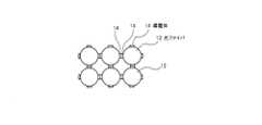
表示部6の各光ファイバ12は、図2に示すように、例えば格子状にX軸方向およびY軸方向に規則的に配列されており、図1(b)中のZ軸方向である光軸方向に移動可能に支持されている。これら光ファイバ12は、図示しない付勢部材によって、光ファイバ12の端面を表示面11aに当接させるように光軸方向に付勢されている。このため、光軸方向に移動された光ファイバ12は、表示パネル11の押し込み力が解除されると、付勢部材の付勢力によって光軸方向に移動され、光ファイバ12の端面を表示面11aに当接させた初期位置に復帰される。 As shown in FIG. 2, the
また、図3および図4(a),図4(b)に示すように、隣接する光ファイバ12同士の各外周面には、互いに当接する位置に導電体14がそれぞれ設けられている。したがって、光ファイバ12には、X軸方向およびY軸方向に沿って導電体14が配置されている。また、各光ファイバ12の外周面の対向する位置に配置された導電体14は、図4(a)に示すように、接続配線16を介して電気的に接続されており、各導電体14を介した各光ファイバ12の導通状態が検出回路7によって検出される。 Further, as shown in FIGS. 3, 4 (a), and 4 (b),
表示部6の表示素子13は、光ファイバ12の端部に配置されており、各光ファイバ12が各画素のRGB(光の三原色)に対応して配置されている。なお、表示素子13は、図示しない光ファイバ12が光軸方向に移動されたときであっても、光ファイバ12の端部と各画素との光学的な接続状態が変化しないように接続されている。 The display element 13 of the display unit 6 is arranged at the end of the
検出回路7は、光ファイバ12の導電体14と電気的に接続されており、隣接する光ファイバ12に設けられた各導電体14の導通状態が解除されることで、押し込まれて光軸方向に移動された光ファイバ12を検出し、表示パネル11の押し込み箇所を検出するように構成されている。この検出回路7は、例えばキーボードのキーの押し込み状態を検出する構成と同様にされている。 The
なお、検出回路7は、上述したような導電体14同士の導通状態が解除されたことを検出する機械的方式に限らず、例えば、光ファイバ12群に磁界を印加しこの磁界中を移動する導電体14を検出するような電磁誘導方式によって光軸方向に移動された光ファイバ12が検出されるように構成されてもよい。 The
以上のように構成された表示装置について、表示パネル11を押し込み操作したときの光ファイバ12の動作を説明する。 With respect to the display device configured as described above, the operation of the
図5(a)に示すように、表示装置では、表示パネル11の表示面11aが押し込み操作されていないとき、各光ファイバ12の導電体14同士が当接されており、各光ファイバ12が導電体14を介してX軸方向およびY軸方向に対してそれぞれ導通されている。導電体14を介して導通されている状態で、抵抗値はほぼ「0」Ωになっている。 As shown in FIG. 5A, in the display device, when the display surface 11a of the
続いて、表示パネル11が押し込み操作されたとき、表示パネル11の押し込み箇所が撓み、図5(b)に示すように、押し込み箇所に対応する光ファイバ12がZ軸方向である光軸方向に移動される。光ファイバ12が光軸方向に移動されることで、隣接する光ファイバ12の導電体14との導通が解除される。このため、検出回路7によって光ファイバ12の導通状態を検出することで、移動された光ファイバ12を検出することが可能になり、表示パネル11の押し込み箇所が検出される。また、光軸方向に移動された光ファイバ12は、表示パネル11の押し込み力が解除されると、付勢部材によって光ファイバ12の端面を表示面11aに当接させた初期位置に復帰される。 Subsequently, when the
上述したように、表示装置は、表示パネル11の表示面11aに光軸方向の端面が当接されて配列され、光軸方向に移動可能に設けられた複数の光ファイバ12を有する表示部6を備えることによって、表示パネル11の押し込み操作時の変位量が良好に確保されるので、押し込み操作時に得られる操作感触を向上することができる。したがって、この表示装置によれば、あたかも操作ボタンのような操作感触を得ることができる。 As described above, the display device is arranged with the display surface 11a of the
なお、上述した実施形態では、表示部6が、光ファイバ12が各画素のRGBに対応して配置された表示素子13を有する構成が採られたが、各光ファイバ12に対応して、発光素子として発光ダイオード(不図示)が配置されて構成されてもよい。この構成の場合には、各光ファイバ12の端部にRGBの発光ダイオードがそれぞれ配置される。 In the above-described embodiment, the display unit 6 is configured to include the display element 13 in which the
6 表示部
7 検出回路
11 表示パネル
11a 表示面
12 光ファイバ
13 表示素子
14 導電体
16 接続配線6
Claims (5)
Translated fromJapanese前記光ファイバの前記端面を前記表示面に当接させるように前記光ファイバを付勢する付勢部材と、
前記光ファイバが移動されたことを検出する検出手段と、
を備え、
隣接する前記光ファイバ同士の各外周面の対向する位置には、互いに電気的に接続された導電体がそれぞれ設けられ、
前記検出手段は、前記各導体体と電気的に接続され、前記各導電体の導通状態を検出する表示装置。A display panel having flexibility; and a plurality of optical fibers arranged in contact with an end surface in the optical axis direction on the display surface of the display panel, and each optical fiber is provided to be movable in the optical axis direction A display unit for displaying information on the display panel via each optical fiber;
A biasing member that biases the optical fiber so that the end surface of the optical fiber is brought into contact with the display surface;
Detecting means for detecting that the optical fiber has been moved;
Equipped witha,
Conductors that are electrically connected to each other are provided at opposing positions on the outer peripheral surfaces of the adjacent optical fibers,
The detection unit is a display devicethat is electrically connected to the conductors and detects a conduction state of the conductors .
Priority Applications (1)
| Application Number | Priority Date | Filing Date | Title |
|---|---|---|---|
| JP2007051535AJP4355729B2 (en) | 2007-03-01 | 2007-03-01 | Display device |
Applications Claiming Priority (1)
| Application Number | Priority Date | Filing Date | Title |
|---|---|---|---|
| JP2007051535AJP4355729B2 (en) | 2007-03-01 | 2007-03-01 | Display device |
Publications (2)
| Publication Number | Publication Date |
|---|---|
| JP2008217224A JP2008217224A (en) | 2008-09-18 |
| JP4355729B2true JP4355729B2 (en) | 2009-11-04 |
Family
ID=39837219
Family Applications (1)
| Application Number | Title | Priority Date | Filing Date |
|---|---|---|---|
| JP2007051535AExpired - Fee RelatedJP4355729B2 (en) | 2007-03-01 | 2007-03-01 | Display device |
Country Status (1)
| Country | Link |
|---|---|
| JP (1) | JP4355729B2 (en) |
Families Citing this family (3)
| Publication number | Priority date | Publication date | Assignee | Title |
|---|---|---|---|---|
| KR101113769B1 (en) | 2010-04-16 | 2012-02-27 | 한국표준과학연구원 | A Resistive tactile sensor and the method for manufacturing thereof and the method for measuring tactile information thereof |
| TR201606367A2 (en)* | 2016-05-13 | 2017-11-21 | Sensobright Ind Llc | A touch panel. |
| WO2022230330A1 (en)* | 2021-04-26 | 2022-11-03 | ソニーグループ株式会社 | Information processing device, information processing method, and program |
- 2007
- 2007-03-01JPJP2007051535Apatent/JP4355729B2/ennot_activeExpired - Fee Related
Also Published As
| Publication number | Publication date |
|---|---|
| JP2008217224A (en) | 2008-09-18 |
Similar Documents
| Publication | Publication Date | Title |
|---|---|---|
| US20230359311A1 (en) | Electronic equipment | |
| US20210349495A1 (en) | Virtual reality viewer and input mechanism | |
| CN103412618B (en) | Input equipment layer with it is nested | |
| US9831871B2 (en) | Touch panel comprising a piezoelectric material | |
| JP5871307B2 (en) | Position detection sensor unit and position detection device | |
| US20120120019A1 (en) | External input device for electrostatic capacitance-type touch panel | |
| JP4860554B2 (en) | Input panel and input device | |
| US20070285402A1 (en) | Mobile terminal and method of displaying image thereof | |
| JP4355729B2 (en) | Display device | |
| JP2005190950A (en) | Input device | |
| KR101426770B1 (en) | Jig for touch-pen grip | |
| JP5057937B2 (en) | Portable electronic devices | |
| JP2018073731A (en) | Electronic apparatus with toggle switch | |
| JP5789290B2 (en) | Touch panel | |
| KR20080024414A (en) | Input device and portable terminal including same | |
| KR101032995B1 (en) | Signal input device for electronic products | |
| JP2017129920A (en) | Input device | |
| JP2014075022A (en) | Input device | |
| JP4929035B2 (en) | Electronics | |
| JP6143686B2 (en) | Electronics | |
| JP2022143861A (en) | Key sheet and display device | |
| JP2011128779A (en) | Touch panel input apparatus | |
| JP2013058125A (en) | Input device and electronic apparatus using the same | |
| JP2011113453A (en) | Touch panel | |
| JP2012053738A (en) | Input device and electronic apparatus |
Legal Events
| Date | Code | Title | Description |
|---|---|---|---|
| A131 | Notification of reasons for refusal | Free format text:JAPANESE INTERMEDIATE CODE: A131 Effective date:20090408 | |
| A521 | Request for written amendment filed | Free format text:JAPANESE INTERMEDIATE CODE: A523 Effective date:20090604 | |
| TRDD | Decision of grant or rejection written | ||
| A01 | Written decision to grant a patent or to grant a registration (utility model) | Free format text:JAPANESE INTERMEDIATE CODE: A01 Effective date:20090722 | |
| A01 | Written decision to grant a patent or to grant a registration (utility model) | Free format text:JAPANESE INTERMEDIATE CODE: A01 | |
| A61 | First payment of annual fees (during grant procedure) | Free format text:JAPANESE INTERMEDIATE CODE: A61 Effective date:20090803 | |
| R150 | Certificate of patent or registration of utility model | Ref document number:4355729 Country of ref document:JP Free format text:JAPANESE INTERMEDIATE CODE: R150 Free format text:JAPANESE INTERMEDIATE CODE: R150 | |
| FPAY | Renewal fee payment (event date is renewal date of database) | Free format text:PAYMENT UNTIL: 20120807 Year of fee payment:3 | |
| FPAY | Renewal fee payment (event date is renewal date of database) | Free format text:PAYMENT UNTIL: 20130807 Year of fee payment:4 | |
| S533 | Written request for registration of change of name | Free format text:JAPANESE INTERMEDIATE CODE: R313533 | |
| R350 | Written notification of registration of transfer | Free format text:JAPANESE INTERMEDIATE CODE: R350 | |
| LAPS | Cancellation because of no payment of annual fees |