JP4351806B2 - Improved technique for etching using a photoresist mask. - Google Patents
Improved technique for etching using a photoresist mask.Download PDFInfo
- Publication number
- JP4351806B2 JP4351806B2JP2000525911AJP2000525911AJP4351806B2JP 4351806 B2JP4351806 B2JP 4351806B2JP 2000525911 AJP2000525911 AJP 2000525911AJP 2000525911 AJP2000525911 AJP 2000525911AJP 4351806 B2JP4351806 B2JP 4351806B2
- Authority
- JP
- Japan
- Prior art keywords
- plasma
- etching
- photoresist mask
- photoresist
- nitride layer
- Prior art date
- Legal status (The legal status is an assumption and is not a legal conclusion. Google has not performed a legal analysis and makes no representation as to the accuracy of the status listed.)
- Expired - Fee Related
Links
- 229920002120photoresistant polymerPolymers0.000titleclaimsdescription184
- 238000000034methodMethods0.000titleclaimsdescription94
- 238000005530etchingMethods0.000titleclaimsdescription71
- 238000012545processingMethods0.000claimsdescription68
- 150000004767nitridesChemical class0.000claimsdescription65
- 230000008569processEffects0.000claimsdescription37
- 239000000460chlorineSubstances0.000claimsdescription36
- 239000000758substrateSubstances0.000claimsdescription36
- 239000007789gasSubstances0.000claimsdescription34
- 229910052801chlorineInorganic materials0.000claimsdescription23
- ZAMOUSCENKQFHK-UHFFFAOYSA-NChlorine atomChemical compound[Cl]ZAMOUSCENKQFHK-UHFFFAOYSA-N0.000claimsdescription19
- 238000002161passivationMethods0.000claimsdescription13
- 229920000642polymerPolymers0.000claimsdescription13
- 229910052734heliumInorganic materials0.000claimsdescription10
- 239000001307heliumSubstances0.000claimsdescription8
- SWQJXJOGLNCZEY-UHFFFAOYSA-Nhelium atomChemical compound[He]SWQJXJOGLNCZEY-UHFFFAOYSA-N0.000claimsdescription8
- 238000009832plasma treatmentMethods0.000claimsdescription6
- XUIMIQQOPSSXEZ-UHFFFAOYSA-NSiliconChemical compound[Si]XUIMIQQOPSSXEZ-UHFFFAOYSA-N0.000claimsdescription5
- 229910052710siliconInorganic materials0.000claimsdescription5
- 239000010703siliconSubstances0.000claimsdescription5
- 150000003839saltsChemical class0.000claims12
- KRHYYFGTRYWZRS-UHFFFAOYSA-MFluoride anionChemical compound[F-]KRHYYFGTRYWZRS-UHFFFAOYSA-M0.000claims2
- 238000009616inductively coupled plasmaMethods0.000claims1
- 210000002381plasmaAnatomy0.000description92
- 238000010849ion bombardmentMethods0.000description10
- 239000000463materialSubstances0.000description8
- 238000002203pretreatmentMethods0.000description7
- 238000004519manufacturing processMethods0.000description6
- 239000004065semiconductorSubstances0.000description5
- YCKRFDGAMUMZLT-UHFFFAOYSA-NFluorine atomChemical compound[F]YCKRFDGAMUMZLT-UHFFFAOYSA-N0.000description4
- 239000006117anti-reflective coatingSubstances0.000description4
- 238000009826distributionMethods0.000description4
- 229910052731fluorineInorganic materials0.000description4
- 239000011737fluorineSubstances0.000description4
- 230000001965increasing effectEffects0.000description4
- 238000000206photolithographyMethods0.000description4
- 238000010586diagramMethods0.000description3
- 150000002500ionsChemical class0.000description3
- IJGRMHOSHXDMSA-UHFFFAOYSA-NAtomic nitrogenChemical compoundN#NIJGRMHOSHXDMSA-UHFFFAOYSA-N0.000description2
- CPELXLSAUQHCOX-UHFFFAOYSA-NHydrogen bromideChemical compoundBrCPELXLSAUQHCOX-UHFFFAOYSA-N0.000description2
- 230000015572biosynthetic processEffects0.000description2
- 238000001816coolingMethods0.000description2
- 238000004518low pressure chemical vapour depositionMethods0.000description2
- 230000007246mechanismEffects0.000description2
- 230000004048modificationEffects0.000description2
- 238000012986modificationMethods0.000description2
- 230000003647oxidationEffects0.000description2
- 238000007254oxidation reactionMethods0.000description2
- 238000006467substitution reactionMethods0.000description2
- 229910004298SiO 2Inorganic materials0.000description1
- 239000000654additiveSubstances0.000description1
- 230000000996additive effectEffects0.000description1
- 238000013459approachMethods0.000description1
- QVGXLLKOCUKJST-UHFFFAOYSA-Natomic oxygenChemical compound[O]QVGXLLKOCUKJST-UHFFFAOYSA-N0.000description1
- 239000006227byproductSubstances0.000description1
- 230000003247decreasing effectEffects0.000description1
- 238000000151depositionMethods0.000description1
- 230000008021depositionEffects0.000description1
- 238000007599dischargingMethods0.000description1
- 230000002708enhancing effectEffects0.000description1
- 239000011521glassSubstances0.000description1
- 229910000042hydrogen bromideInorganic materials0.000description1
- 230000006698inductionEffects0.000description1
- 238000001459lithographyMethods0.000description1
- 229910052757nitrogenInorganic materials0.000description1
- 239000001301oxygenSubstances0.000description1
- 229910052760oxygenInorganic materials0.000description1
- 238000000059patterningMethods0.000description1
- 230000009467reductionEffects0.000description1
- 238000011160researchMethods0.000description1
- 238000007789sealingMethods0.000description1
- 238000009279wet oxidation reactionMethods0.000description1
Images


Classifications
- H—ELECTRICITY
- H01—ELECTRIC ELEMENTS
- H01L—SEMICONDUCTOR DEVICES NOT COVERED BY CLASS H10
- H01L21/00—Processes or apparatus adapted for the manufacture or treatment of semiconductor or solid state devices or of parts thereof
- H01L21/02—Manufacture or treatment of semiconductor devices or of parts thereof
- H01L21/027—Making masks on semiconductor bodies for further photolithographic processing not provided for in group H01L21/18 or H01L21/34
- H01L21/0271—Making masks on semiconductor bodies for further photolithographic processing not provided for in group H01L21/18 or H01L21/34 comprising organic layers
- H01L21/0273—Making masks on semiconductor bodies for further photolithographic processing not provided for in group H01L21/18 or H01L21/34 comprising organic layers characterised by the treatment of photoresist layers
- H—ELECTRICITY
- H01—ELECTRIC ELEMENTS
- H01L—SEMICONDUCTOR DEVICES NOT COVERED BY CLASS H10
- H01L21/00—Processes or apparatus adapted for the manufacture or treatment of semiconductor or solid state devices or of parts thereof
- H01L21/02—Manufacture or treatment of semiconductor devices or of parts thereof
- H01L21/04—Manufacture or treatment of semiconductor devices or of parts thereof the devices having potential barriers, e.g. a PN junction, depletion layer or carrier concentration layer
- H01L21/18—Manufacture or treatment of semiconductor devices or of parts thereof the devices having potential barriers, e.g. a PN junction, depletion layer or carrier concentration layer the devices having semiconductor bodies comprising elements of Group IV of the Periodic Table or AIIIBV compounds with or without impurities, e.g. doping materials
- H01L21/30—Treatment of semiconductor bodies using processes or apparatus not provided for in groups H01L21/20 - H01L21/26
- H01L21/31—Treatment of semiconductor bodies using processes or apparatus not provided for in groups H01L21/20 - H01L21/26 to form insulating layers thereon, e.g. for masking or by using photolithographic techniques; After treatment of these layers; Selection of materials for these layers
- H01L21/3105—After-treatment
- H01L21/311—Etching the insulating layers by chemical or physical means
- H01L21/31105—Etching inorganic layers
- H01L21/31111—Etching inorganic layers by chemical means
- H01L21/31116—Etching inorganic layers by chemical means by dry-etching
- G—PHYSICS
- G03—PHOTOGRAPHY; CINEMATOGRAPHY; ANALOGOUS TECHNIQUES USING WAVES OTHER THAN OPTICAL WAVES; ELECTROGRAPHY; HOLOGRAPHY
- G03F—PHOTOMECHANICAL PRODUCTION OF TEXTURED OR PATTERNED SURFACES, e.g. FOR PRINTING, FOR PROCESSING OF SEMICONDUCTOR DEVICES; MATERIALS THEREFOR; ORIGINALS THEREFOR; APPARATUS SPECIALLY ADAPTED THEREFOR
- G03F1/00—Originals for photomechanical production of textured or patterned surfaces, e.g., masks, photo-masks, reticles; Mask blanks or pellicles therefor; Containers specially adapted therefor; Preparation thereof
- G03F1/68—Preparation processes not covered by groups G03F1/20 - G03F1/50
- G03F1/80—Etching
- G—PHYSICS
- G03—PHOTOGRAPHY; CINEMATOGRAPHY; ANALOGOUS TECHNIQUES USING WAVES OTHER THAN OPTICAL WAVES; ELECTROGRAPHY; HOLOGRAPHY
- G03F—PHOTOMECHANICAL PRODUCTION OF TEXTURED OR PATTERNED SURFACES, e.g. FOR PRINTING, FOR PROCESSING OF SEMICONDUCTOR DEVICES; MATERIALS THEREFOR; ORIGINALS THEREFOR; APPARATUS SPECIALLY ADAPTED THEREFOR
- G03F7/00—Photomechanical, e.g. photolithographic, production of textured or patterned surfaces, e.g. printing surfaces; Materials therefor, e.g. comprising photoresists; Apparatus specially adapted therefor
- G03F7/26—Processing photosensitive materials; Apparatus therefor
- G03F7/40—Treatment after imagewise removal, e.g. baking
- H—ELECTRICITY
- H01—ELECTRIC ELEMENTS
- H01L—SEMICONDUCTOR DEVICES NOT COVERED BY CLASS H10
- H01L21/00—Processes or apparatus adapted for the manufacture or treatment of semiconductor or solid state devices or of parts thereof
- H01L21/02—Manufacture or treatment of semiconductor devices or of parts thereof
- H01L21/04—Manufacture or treatment of semiconductor devices or of parts thereof the devices having potential barriers, e.g. a PN junction, depletion layer or carrier concentration layer
- H01L21/18—Manufacture or treatment of semiconductor devices or of parts thereof the devices having potential barriers, e.g. a PN junction, depletion layer or carrier concentration layer the devices having semiconductor bodies comprising elements of Group IV of the Periodic Table or AIIIBV compounds with or without impurities, e.g. doping materials
- H01L21/30—Treatment of semiconductor bodies using processes or apparatus not provided for in groups H01L21/20 - H01L21/26
- H01L21/302—Treatment of semiconductor bodies using processes or apparatus not provided for in groups H01L21/20 - H01L21/26 to change their surface-physical characteristics or shape, e.g. etching, polishing, cutting
- H01L21/306—Chemical or electrical treatment, e.g. electrolytic etching
- H01L21/3065—Plasma etching; Reactive-ion etching
- H—ELECTRICITY
- H01—ELECTRIC ELEMENTS
- H01L—SEMICONDUCTOR DEVICES NOT COVERED BY CLASS H10
- H01L21/00—Processes or apparatus adapted for the manufacture or treatment of semiconductor or solid state devices or of parts thereof
- H01L21/02—Manufacture or treatment of semiconductor devices or of parts thereof
- H01L21/04—Manufacture or treatment of semiconductor devices or of parts thereof the devices having potential barriers, e.g. a PN junction, depletion layer or carrier concentration layer
- H01L21/18—Manufacture or treatment of semiconductor devices or of parts thereof the devices having potential barriers, e.g. a PN junction, depletion layer or carrier concentration layer the devices having semiconductor bodies comprising elements of Group IV of the Periodic Table or AIIIBV compounds with or without impurities, e.g. doping materials
- H01L21/30—Treatment of semiconductor bodies using processes or apparatus not provided for in groups H01L21/20 - H01L21/26
- H01L21/31—Treatment of semiconductor bodies using processes or apparatus not provided for in groups H01L21/20 - H01L21/26 to form insulating layers thereon, e.g. for masking or by using photolithographic techniques; After treatment of these layers; Selection of materials for these layers
- H01L21/3105—After-treatment
- H01L21/311—Etching the insulating layers by chemical or physical means
- H01L21/31127—Etching organic layers
- H01L21/31133—Etching organic layers by chemical means
- H01L21/31138—Etching organic layers by chemical means by dry-etching
- H—ELECTRICITY
- H01—ELECTRIC ELEMENTS
- H01L—SEMICONDUCTOR DEVICES NOT COVERED BY CLASS H10
- H01L21/00—Processes or apparatus adapted for the manufacture or treatment of semiconductor or solid state devices or of parts thereof
- H01L21/02—Manufacture or treatment of semiconductor devices or of parts thereof
- H01L21/04—Manufacture or treatment of semiconductor devices or of parts thereof the devices having potential barriers, e.g. a PN junction, depletion layer or carrier concentration layer
- H01L21/18—Manufacture or treatment of semiconductor devices or of parts thereof the devices having potential barriers, e.g. a PN junction, depletion layer or carrier concentration layer the devices having semiconductor bodies comprising elements of Group IV of the Periodic Table or AIIIBV compounds with or without impurities, e.g. doping materials
- H01L21/30—Treatment of semiconductor bodies using processes or apparatus not provided for in groups H01L21/20 - H01L21/26
- H01L21/31—Treatment of semiconductor bodies using processes or apparatus not provided for in groups H01L21/20 - H01L21/26 to form insulating layers thereon, e.g. for masking or by using photolithographic techniques; After treatment of these layers; Selection of materials for these layers
- H01L21/3105—After-treatment
- H01L21/311—Etching the insulating layers by chemical or physical means
- H01L21/31144—Etching the insulating layers by chemical or physical means using masks
- H—ELECTRICITY
- H01—ELECTRIC ELEMENTS
- H01L—SEMICONDUCTOR DEVICES NOT COVERED BY CLASS H10
- H01L21/00—Processes or apparatus adapted for the manufacture or treatment of semiconductor or solid state devices or of parts thereof
- H01L21/02—Manufacture or treatment of semiconductor devices or of parts thereof
- H01L21/04—Manufacture or treatment of semiconductor devices or of parts thereof the devices having potential barriers, e.g. a PN junction, depletion layer or carrier concentration layer
- H01L21/18—Manufacture or treatment of semiconductor devices or of parts thereof the devices having potential barriers, e.g. a PN junction, depletion layer or carrier concentration layer the devices having semiconductor bodies comprising elements of Group IV of the Periodic Table or AIIIBV compounds with or without impurities, e.g. doping materials
- H01L21/30—Treatment of semiconductor bodies using processes or apparatus not provided for in groups H01L21/20 - H01L21/26
- H01L21/31—Treatment of semiconductor bodies using processes or apparatus not provided for in groups H01L21/20 - H01L21/26 to form insulating layers thereon, e.g. for masking or by using photolithographic techniques; After treatment of these layers; Selection of materials for these layers
- H01L21/3205—Deposition of non-insulating-, e.g. conductive- or resistive-, layers on insulating layers; After-treatment of these layers
- H01L21/321—After treatment
- H01L21/3213—Physical or chemical etching of the layers, e.g. to produce a patterned layer from a pre-deposited extensive layer
- H01L21/32139—Physical or chemical etching of the layers, e.g. to produce a patterned layer from a pre-deposited extensive layer using masks
Landscapes
- Engineering & Computer Science (AREA)
- Physics & Mathematics (AREA)
- General Physics & Mathematics (AREA)
- Computer Hardware Design (AREA)
- Condensed Matter Physics & Semiconductors (AREA)
- Manufacturing & Machinery (AREA)
- Microelectronics & Electronic Packaging (AREA)
- Power Engineering (AREA)
- Chemical & Material Sciences (AREA)
- Chemical Kinetics & Catalysis (AREA)
- General Chemical & Material Sciences (AREA)
- Inorganic Chemistry (AREA)
- Plasma & Fusion (AREA)
- Drying Of Semiconductors (AREA)
Description
Translated fromJapanese【0001】
【発明の属する技術分野】
この発明は、半導体デバイスの製造に関し、特に、製造の最中にフォトレジストマスクの下の層をエッチングするための改良技術に関する。
【0002】
【発明の背景】
半導体デバイス、すなわち半導体材料を利用した電子デバイスの製造では、基板の上に様々な層を堆積させ、選択的にエッチングすることにより所望のデバイスを形成する。所定の層を選択的にエッチングするために、フォトレジストマスクが一般的に利用される。
【0003】
議論を容易にするため、図1に、基板102の上に配置された複数の層を含む、代表的な積層体100を示した。基板102は、例えばウェーハまたはガラスパネルの形を採ることができ、そこから集積回路またはフラットパネルディスプレイが製作される。図1に示された代表的な積層体は、基板102の上に配置された酸化物(SiO2)層104を含む。酸化物層104は、熱酸化(例えば湿式酸化または乾式酸化)等の適切な酸化物形成工程を使用して形成されるのが典型的である。窒化物(Si3N4等のSixNy)層106は、酸化物層104の上側に配置されて図示されており、低圧CVD(LPCVD)等の適切な窒化物工程を使用して形成されるのが一般的である。積層体100は、例えば集積回路の作用面積等を形成するのに利用しても良い。
【0004】
窒化物層106の選択性エッチングを容易にするため、先ず、例えばスピンオン(spin-on)工程によりフォトレジスト層108を堆積させる。次に、従来のフォトリソグラフィ工程を利用し、フォトレジスト層108をパターン形成してマスクを形成することにより、窒化物層106内の選択領域のエッチングを容易にする。このような技術の1つとして、例えば、フォトレジスト材料を接触式またはステップ式リソグラフィシステム内に露出させてフォトレジスト層108をパターン形成し、このフォトレジスト材料を現像してマスクを形成することにより、後続のエッチング工程を容易にする技術が挙げられる。このようにして形成されるフォトレジストマスクを、図2に示した。その後、フォトレジストの下層のうちマスクで保護されていない領域(例えば、窒化物層106の領域202,204)をエッチングすると、望ましい特徴(造形)が後に残される。
【0005】
エッチング工程の精度は、電子デバイスの密度が増大するにつれて限界に近づく。これは、デバイスが密接に集積されていると、エッチングプロフィルを慎重に制御して、例えば隣接特徴間の偶発的短絡等を防ぐ必要があるからである。デバイスのサイズがサブミクロンの領域(例えば0.25ミクロンまたはそれ未満)に到達すると、従来のフォトレジストマスクでは、後続のエッチング工程で困難を生じることがある。
【0006】
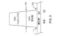
従来のフォトレジストマスクを改良することなく利用してフォトレジスト下層(例えば窒化物層106)をエッチングする際の問題点を容易に議論するため、エッチング後の図2の窒化物層106を、部分的に図3に示した。図3には、例えば、図2のフォトレジスト特徴の1つであるフォトレジスト特徴108(a)が示されている。また、窒化物をエッチングした後に残留する窒化物材料である、窒化物特徴106(a)も示されている。
【0007】
図3に示されるように、フォトレジスト特徴108(a)はテーパプロフィルを示す。すなわち、フォトレジストの垂直な側壁と基板の平面とが形成する角度が直角未満である。フォトレジスト特徴のテーパプロフィルは、窒化物のエッチング工程が進行するに伴って、フォトレジスト層108をパターン形成するフォトリソグラフィ工程、および/または後続の窒化物エッチング工程の等方性要素が原因で、窒化物層内を下向きに伝わっていく。このため、窒化物特徴106(a)もまた、底部の窒化物特徴(122)が頂部におけるそれ(124)よりも幾分幅広のテーパプロフィルを示す。
【0008】
窒化物特徴106(a)のテーパプロフィルは、エッチング特徴のプロフィルが制御しにくいことを表している。プロフィル制御が不充分だと、得られる窒化物特徴の微小寸法(CD:critical dimension)制御が困難になる。プロフィル制御および/またはCD制御が特に不充分だと、得られるエッチング特徴が、現代の高密度(例えばサブミクロンまたはそれ以下)デバイス製造への使用に不適切となる恐れがある。
【0009】
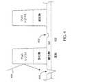
エッチングプロフィルは、窒化物のエッチングにおいて、イオン衝撃要素または物理的エッチング要素を増すことにより改良できると考えられてきた。平行平板電極型のプラズマシステムでは、イオン衝撃は、例えば、プラズマ処理チャンバのRF電源の設定値を上げる、エッチング圧力を下げる、平行平板電極間の間隙を小さくする等の方法(またはこれらの任意の組み合わせ)で増大させることができる。イオン衝撃の増大は、より垂直な側壁の形成を可能にするが、同時に幾つかの欠点も生じる。
【0010】
例えば、物理的工程であるイオン衝撃は、異なる層間における選択性を特に有さない。このため、エッチングを望まない層を含む全ての層を、無差別にエッチングする傾向にある。イオン衝撃工程はさらに、精確な制御が比較的困難である。このため、エッチングのイオン衝撃要素を増大させると、他の層または/および基板の他の特徴が、意図せぬ損傷を受ける恐れがある。図4に示されるように、イオン衝撃要素の増大は、例えば、窒化物の下層である酸化物層104(領域402)および/または基板102(領域404)に、望ましくない損傷を与える恐れがある。
【0011】
以上から、半導体デバイスの製造において、フォトレジスト層の下層をエッチングするための改良技術が望まれていることがわかる。
【0012】
【発明の概要】
本発明の一実施形態は、フォトレジストの下層をエッチングするための方法に関する。この方法は、フォトレジストの下層およびその上のフォトレジストマスクを有した基板を提供する工程を備える。この方法はさらに、塩素ベースのプラズマ(chlorine-based plasma)を使用して、プラズマ処理チャンバ内でフォトレジストマスクを処理する工程を備える。この処理工程は、フォトレジストマスクの少なくとも一部分をエッチングし、このフォトレジストマスクの垂直の側壁にパッシベーションポリマを堆積させるように構成される。この方法はさらに、上述した処理工程に続くエッチング工程において、フォトレジストマスクを使用してフォトレジストの下層をエッチングする工程を備える。
【0013】
本発明の別の実施形態は、基板上に配置されたフォトレジスト下層をエッチングする際の、プロフィル制御を改良するための方法に関する。このフォトレジスト下層は、フォトレジストマスクの下に配置されている。この方法は、フォトレジスト下層およびフォトレジストマスクを有した基板を、プラズマ処理チャンバ内に配置する工程を備える。この方法はまた、塩素含有エッチャントソースガスを、プラズマ処理チャンバ内に流す工程を備える。この方法はさらに、塩素含有エッチャントソースガスからプラズマを発生させ、プラズマ処理チャンバ内で塩素ベースのプラズマを形成させる工程を備える。この方法はさらにまた、塩素ベースのプラズマを使用して、プラズマ処理チャンバ内でフォトレジストマスクを処理する工程を備える。フォトレジストの処理は、フォトレジストマスクの少なくとも一部分をエッチングして、フォトレジスト下層をエッチングすることなくフォトレジストマスクの垂直の側壁にパッシベーションポリマを堆積させるように、構成される。
【0014】
本発明のさらに別の実施形態は、シリコン基板上に配置された窒化物層をエッチングする際の、プロフィル制御を改良するための方法に関する。この窒化物層は、フォトレジストマスクの下に配置されている。この方法は、窒化物層およびフォトレジストマスクを含んだ基板を、プラズマ処理チャンバ内に配置する工程を備える。この方法はまた、塩素含有エッチャントソースガスを、プラズマ処理チャンバ内に流す工程を備える。この方法はさらに、塩素含有エッチャントソースガスからプラズマを発生させて、プラズマ処理チャンバ内で塩素ベースのプラズマを形成させる工程を備える。この方法はさらにまた、塩素プラズマを使用して、プラズマ処理チャンバ内でフォトレジストマスクを処理する工程を備える。フォトレジストの処理は、フォトレジストマスクの少なくとも一部分をエッチングして、窒化物層をエッチングすることなくフォトレジストマスクの垂直の側壁にパッシベーションポリマを堆積させるように、構成される。
【0015】
本発明の上述したおよびその他の特徴を、添付した図面と関連させながら、以下に続く発明の詳細な説明においてさらに詳しく説明する。
【0016】
【発明の実施の形態】
添付の図面に示される幾つかの好ましい実施形態にもとづいて、本発明を詳しく説明する。以下の説明では、本発明の完全な理解を促す目的で多くの項目を特定している。しかしながら、当業者には明らかなように、本発明は、これらの項目の一部または全てを特定しなくても実施することができる。また、本発明を不必要に不明瞭化するのを避けるため、周知の処理工程および/または構造の説明は省略した。
【0017】
本発明の一特徴によれば、フォトレジスト下層のエッチングプロフィルは、フォトレジスト下層のエッチングに先立ちフォトレジストマスクにプラズマ処理を施すことにより改良される。ここで、フォトレジスト下層とは、フォトレジストマスクの下に横たわり、このエッチングマスクを使用して後続の工程でエッチングされるように構成される、1層またはそれ以上の層を指す。また、添付した図面に示される層は例示のみを目的としていること、処理後のフォトレジストマスクを使用してエッチングされる異なる積層体には異なる層が存在し得ることを、心に留めておく必要がある。さらに、図示される層と層の間には、1層またはそれ以上の層が存在しても良い。このような層は、例えば、密着性強化層、種子層、またはその他任意の層を含んでも良い。このため、ここで使用する「上」、「上層」、「下」、「下層」等の位置関係を表す用語は、層と層が直接接触することを要求するものではない。
【0018】
本発明の一実施形態において、プラズマによるフォトレジストの前処理は、フォトレジスト特徴の垂直面に沿ってパッシベーションポリマを堆積させ、このフォトレジスト特徴のテーパを低減するように構成される。フォトレジスト下層のエッチングに先立ちフォトレジスト特徴のプロフィルを改良することにより、エッチングでフォトレジスト下層から形成される特徴のプロフィルを改良することができる。
【0019】
一方または加えて、フォトレジスト特徴の垂直側壁上のパッシベーションポリマは、フォトレジスト下層のエッチング中においてフォトレジスト特徴のプロフィル維持を促進することにより、後続のエッチングでフォトレジスト下層から形成される特徴の、プロフィル制御の改良を促進する。この改良技術を利用すると、エッチングでフォトレジスト下層から形成される特徴のプロフィルを、イオン衝撃要素の大きいエッチングを必要とすることなく有利に制御することができる。物理的エッチング要素が大きくないため、フォトレジスト下層のエッチング中に他の層および/または基板の他の領域が受ける意図しない損傷を、有利に最小化することができる。
【0020】
図面を参照にして行う以下の説明から、本発明の特徴および利点が一層明瞭となる。本発明の一特徴によれば、フォトレジスト下層のエッチングに先立ち、その上にフォトレジスト下層(例えば図2の窒化物層106)およびフォトレジストマスク(例えば図2のフォトレジストマスク108)を有する基板に対して、先ずプラズマ環境におけるフォトレジストマスクの処理を実施する。このフォトレジストのプラズマ前処理は、フォトレジスト下層を実際にエッチングするのに先立ち、それとは異なるプラズマを利用してフォトレジストマスクを処理するという点において、フォトレジスト下層のエッチングとは別個の工程である。フォトレジスト下層のなかには、フォトレジストのプラズマ前処理工程中にエッチングされる材料もあるが、フォトレジストのプラズマ前処理は、実際にフォトレジスト下層をエッチングする後続のエッチング工程よりも遅い速度でフォトレジスト下層(例えば窒化物層)をエッチングすることが好ましい(ただし必然ではない)。
【0021】
本発明の一実施形態では、もし必要であれば、フォトレジストのプラズマ前処理およびフォトレジスト下層のエッチングをともに、単一のプラズマ処理チャンバ内で(異なる2工程に分けて)実施しても良い。事実、フォトレジストのプラズマ前処理およびフォトレジスト下層のエッチングは、同一のプラズマ処理チャンバ内で真空封止を破ることなく実施しても良い。しかしながら、フォトレジストのプラズマ前処理は、フォトレジスト下層のエッチングとは異なるプラズマ処理チャンバ内で実施しても良い。
【0022】
本発明の実施形態では、フォトレジストのプラズマ前処理を、カリフォルニア州フリーモント市所在のラム・リサーチ・コーポレーションによる4420XL(商標)として知られる平行平板電極型プラズマ処理システムを利用して実施する。しかしながら、任意の高密度・低圧プラズマシステム等(容量結合、誘電結合、電子サイクロトロン共鳴[ECR]の各システムを含む)の他の適切なプラズマ処理システムもまた、同様に利用され得る。フォトレジストプラズマ前処理はまた、例えば、適切なダイオード型またはトライオード型のシステムで実施しても良い。このように、ここでは議論を容易にするため4420XL(商標)を使用してはいるものの、本発明によるフォトレジストプラズマ前処理(および/または後続のフォトレジスト下層のエッチング)が任意の適切なプラズマ処理システムを使用して実施し得ることに留意すべきである。
【0023】
図5に示されるように、プラズマ処理システム500はプラズマ処理チャンバ502を備える。チャンバ502の上方には電極504が配置されており、図5の例では、シャワーヘッドを有したガス分布装置の構成により具現化されている。電極504は、整合回路網508を介して高周波(RF)ジェネレータ506により通電される。図5の例では、RFジェネレータ506は周波数が約13.56MHzのRFエネルギを供給するが、他の適した周波数を利用しても良い。
【0024】
シャワーヘッド504は、自身と基板514の間に位置するRF誘導プラズマ領域512に、ガス状のエッチャントソースガスを放出するためのガス分布装置である。しかしながら、ガス分布リング、またはチャンバの壁上に配置された単なるポート等の、他のガス分布装置を利用しても良い。フォトレジストマスクの下にフォトレジスト下層が配置された基板514を、プラズマ処理チャンバ502内に導入し、チャック516の上に配置する。図5の例では、チャック516は静電(ESC)チャックであるが、例えば真空チャック、メカニカルチャック、または単なるワークホルダでも良い。
【0025】
ヘリウム等の熱交換ガスを、チャック516と基板514の間の領域に導入し、基板とチャックの間の熱交換を制御して、均一で反復性のある処理結果を確保しても良い。フォトレジストのプラズマ前処理(または後続のフォトレジスト下層のエッチング)を容易にするため、適切なエッチャントソースガスをシャワーヘッド504から流し、RFジェネレータ506が供給するRFエネルギでプラズマを発生させる。フォトレジストのプラズマ前処理の最中(または後続のエッチングの最中)には、形成された副生物のガスの一部が、(例えば適切なターボポンプ構成を使用して)排気ポート522を経てチャンバ502から排出される。図5の例では、排気ポート522はリング状の構造を有し、チャンバの底部に配置されているが、他の任意の適切な構造を利用しても良い。絶対的に必要ではないが、電極502と基板114との間の間隙の大きさを(例えば電極および/または基板を移動させることにより)変化させ、処理の最適化を図っても良い。
【0026】
本発明の実施形態では、フォトレジストマスクのプラズマ処理を、塩素ベースのプラズマを使用して実施する。塩素ベースのプラズマは、塩素含有ガス(例えばCl2)を含有する適切なエッチャントソースガスから形成することができる。また、HBr、酸素、窒素、および/またはHe等の追加のガスを、(例えばCl2ガスに)添加しても良い。
【0027】
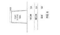
塩素ベースのプラズマは、フォトレジスト特徴の一部をエッチングするように構成される。フォトレジストのプラズマ処理の最中には、フォトレジスト特徴の垂直な側壁に沿ってパッシベーションポリマが堆積される。図6によれば、フォトレジストのプラズマ前処理は、フォトレジスト特徴108(a)の一部分602をエッチングで除去し、フォトレジスト特徴の垂直な側壁に沿ってパッシベーションポリマを堆積させる。理解を容易にするため、図6では、処理前のフォトレジスト特徴を点線で、プラズマ前処理後のフォトレジスト特徴を実線で示している。パッシベーションポリマの堆積は、フォトレジスト特徴のテーパの軽減を促して、フォトレジスト特徴のプロフィルを改良できると信じられている。上述したように、この改良プロフィルは、エッチングでフォトレジスト下層から形成される特徴内を、下向きに移動または伝播する。
【0028】
フォトレジスト下層内の露出した材料のなかには、フォトレジストのプラズマ処理中にエッチングされ得るものもある。例えば、代表的なフォトレジストプラズマ前処理中には、数百オングストロームの窒化物材料がエッチングで除去される。しかしながら、フォトレジストプラズマ前処理の工程は、実質的にはフォトレジスト下層内までエッチングしないことが好ましい。例えば、フォトレジストプラズマ前処理中にエッチングで除去されるフォトレジスト下層(例えば窒化物層)は、その厚さの5〜25%未満であることが好ましい。
【0029】
フォトレジストプラズマ前処理中にエッチングされる窒化物材料のなかには、フォトレジスト特徴108(a)の垂直側壁に沿って堆積されるパッシベーションポリマ内に組み込まれ得るものもある。フォトレジストプラズマ前処理中にエッチングされた材料が組み込まれると、構築された側壁は、後続のフォトレジスト下層のエッチング工程に対して耐性を向上させると信じられている。その結果、後続のフォトレジスト下層のエッチング工程において、除去されるフォトレジストの垂直側壁の量が減少するため、フォトレジストのプロフィルがより良く維持されるようになる。
【0030】
フォトレジストマスクのプラズマ処理後、フォトレジスト下層は、プラズマエッチングチャンバ内で適切なエッチャントを使用してエッチングされる。図7の例では、窒化物層106は、フッ素含有ソースガスを使用した従来のフッ素ベースのプラズマを使用してエッチングされる。フッ素含有ソースガスは例えば、SF6、He/SF6、SF6/He/CHF3、SF6/He/HBr、SF6/O2、CF4、CF4/Heである。もし必要であれば、CHF3またはヘリウム(He)等の添加物を添加しても良い。本発明の一実施形態では、窒化物層のエッチングは、プラズマ処理工程の直後に同一のプラズマ処理チャンバ(例えば上述した4420XL[商標])内で実施される。このため真空封止を破る必要がなく、基板のスループットを有利に向上させることができる。ただし、これは必要条件ではなく、フォトレジスト下層のエッチングは、任意の適切なプラズマ処理チャンバ内で実施しても良い。
【0031】
図7に示されるように、フォトレジスト特徴108(a)の改良プロフィルは、窒化物特徴106(a)に向けて下向きに移動または伝播する。このため、下層である窒化物特徴106(a)のプロフィル制御が有利に達成される。ここで、この改良プロフィル制御が従来技術と異なり、窒化物エッチング工程のイオン衝撃要素を増大させる必要がない点に注意が必要である。このプロフィル制御の改良により、エッチング後の下層窒化物特徴の微小寸法(CD)制御も改良されるため、エッチング後の窒化物特徴を、現代の高密度デバイスの製造への使用に一層適切なものとすることができる。
【0032】
さらに、フォトレジストプラズマ前処理がマイクロトレンチング(microtrenching)を減らせることがわかった。マイクロトレンチングは、エッチングされた特徴の足元または疎な領域に、エッチング速度のマイクロローディング(すなわち、密な領域より疎な領域の方でエッチング速度が大きくなる現象)を原因として意図しない溝が形成される現象を指す。マイクロトレンチングは例えば、エッチングされた窒化物特徴106(a)の足元の酸化物層104に(場合によっては基板102そのものにも)溝を形成する恐れがある。メカニズムはまだ完全に解明されていないが、マイクロトレンチは、フォトレジスト下層のエッチング中に、プラズマシースからのイオンがフォトレジスト特徴の垂直側壁に反射して形成されると信じられている。イオンは、例えば図4に示されるように、フォトレジストの垂直側壁で矢印406の方向に反射される。
【0033】
理論に縛られることは望まないが、本発明で開示する工程によりフォトレジストマスクを処理された基板において、マイクロトレンチングの減少が観測される原因は、1つには、フォトレジスト特徴の高さが減少し、反射されたイオンが跳ね返るための垂直面が減少するためだと信じられている。本発明によるフォトレジストプラズマ前処理工程により前もってフォトレジストマスクを処理された基板では、厳密なメカニズムの如何に関係なく、マイクロトレンチングの実質的な減少が観測される。
【0034】
代表的なフォトレジストプラズマ前処理工程において、厚さ1500オングストロームの窒化物層の下に厚さ100〜150オングストロームの酸化物層が配置された、8インチのシリコンウェーハを利用する。窒化物層は、厚さ約10,000オングストロームのフォトレジストマスクで覆われる。フォトレジストマスクは、幅0.25ミクロンの小開口部を含む様々な幅の開口部を有している。
【0035】
代表的なフォトレジストプラズマ前処理工程は、上述した4420XL(商標)プラズマ処理システムにおいて20秒間実施される。しかしながら、このシステムまたは他のプラズマ処理システムにおけるこの処理工程は、約10〜60秒間持続して良く、より好ましくは約15〜30秒間持続して良いと考えられる。
【0036】
代表的なフォトレジストプラズマ前処理工程において、電力の設定値は約275ワット(W)である。しかしながら、このシステムまたは他のプラズマ処理システムにおける電力の設定値は、約100〜500ワットで良く、より好ましくは約225〜400ワットで良いと考えられる。
【0037】
代表的なフォトレジストプラズマ前処理工程において、チャンバ圧力は約425ミリトール(mT)である。しかしながら、このシステムまたは他のプラズマ処理システムにおけるチャンバ圧力は、約250〜700ミリトールで良く、より好ましくは約300〜500ミリトールで良いと考えられる。
【0038】
代表的なフォトレジストプラズマ前処理工程において、Cl2ガスの流量は標準状態下で約200立方センチメートル毎分(sccm)である。しかしながら、このシステムまたは他のプラズマ処理システムにおけるCl2ガスの流量は、約100〜400sccmで良く、より好ましくは約150〜250sccmで良いと考えられる。
【0039】
代表的なフォトレジストプラズマ前処理工程において、オプションのヘリウムガスの流量は、標準状態下で約400立方センチメートル毎分(sccm)である。しかしながら、このシステムまたは他のプラズマ処理システムにおけるオプションのヘリウムガスの流量は、約0〜500sccmで良く、より好ましくは約300〜500sccmで良いと考えられる。異なるシステムで実施する場合および/または異なるサイズの基板を使用する場合は、流量は変化し得る。しかしながら、上で開示したこれらのガスの比は、適切なプラズマ処理システムにおいてフォトレジストマスクのプラズマ処理を行うのに適していると考えられる。
【0040】
代表的なフォトレジストプラズマ前処理工程において、間隙の設定値は約0.8センチメートル(cm)である。しかしながら、このシステムまたは他のプラズマ処理システムにおける間隙の設定値は約0.6〜1.2cmで良く、より好ましくは約0.7〜1.0cmで良いと考えられる。
【0041】
代表的なフォトレジストプラズマ前処理工程において、ヘリウム冷却時の圧力は約6トール(T)である。しかしながら、このシステムまたは他のプラズマ処理システムにおけるヘリウム冷却時の圧力は約0〜12Tで良く、より好ましくは約0〜10Tで良いと考えられる。
【0042】
代表的なフォトレジストプラズマ前処理工程において、チャックの温度設定値は約40度である。しかしながら、このシステムまたは他のプラズマ処理システムにおけるチャックの温度設定値は約10〜65度で良く、より好ましくは約20〜50度で良いと考えられる。
【0043】
図8は、プロフィル制御および/または微小寸法制御を改良するように構成された、代表的なフォトレジストプラズマ前処理工程で利用される、本発明の一実施形態にもとづく工程の流れ図である。工程802において、エッチング予定のフォトレジスト下層を上に有した基板を提供する。フォトレジスト下層は、パターン形成されたフォトレジストマスクの下に配置されている。一例ではフォトレジスト下層は、薄い酸化物層(例えば、図1の窒化物層106および酸化物層104)を覆う窒化物層である。工程804において、フォトレジストマスクを塩素ベースのプラズマを使用して処理することにより、フォトレジスト特徴の少なくとも一部分をエッチングし、フォトレジストマスクの垂直な側壁上にパッシベーションポリマを堆積させる。工程806において、フォトレジスト下層を適切なエッチャントを使用してエッチングする。窒化物層のエッチングには、上述したようにフッ素ベースのエッチャントを利用しても良い。そして、追加で従来の処理工程を基板に施し、例えばフラットパネルディスプレイ、集積回路(ダイナミックRAM、または他の任意のトランジスタ回路等)等の、望ましい半導体デバイスを形成しても良い。
【0044】
以上、本発明をいくつかの好ましい実施形態にもとづいて説明したが、本発明の範囲内における他の変形物、置換物および等価物を実施することも可能である。例えば、4420XL(商標)プラズマ処理システムに対応する代表的な工程パラメータの範囲を挙げたが、本発明の開示を読んだ当業者が別のプラズマ処理システムを提供した際には、これらの値を必要に応じて変動させても良い。さらに別の例では、積層体のフォトレジスト層の下に、フォトリソグラフィのための反射防止膜(ARC:antireflective coating)または底部反射防止膜(BARC:bottom antireflective coating)層(有機または無機のいずれかで良い)を利用しても良い。これらのARCまたはBARC層は、フォトレジストプラズマ前処理に先立ち既にパターン形成されいても良いし、またはパターン形成されていなくても良い。また、本発明による方法および装置は、多くの代替方式により具現化しても良い。このため、添付した請求の範囲は、本発明の真の趣旨および範囲を逸脱しない全ての変形物、置換物および等価物を含むものとして解釈される。
【図面の簡単な説明】
【図1】 議論を容易にする目的で基板上に複数の層を配置された、代表的な積層体を示した図である。
【図2】 従来のフォトリソグラフィ工程を使用してパターン形成されたフォトレジスト層を含む、図1の積層体を示した図である。
【図3】 窒化物がエッチングされた後の図2の窒化物層を、部分的に示した図である。
【図4】 プロフィル制御および/または微小寸法制御を改良する目的で、窒化物のエッチングにおけるイオン衝撃要素を増大させた際に、窒化物の下層である酸化物層または基板が受ける損傷を示した図である。
【図5】 本発明によるフォトレジストプラズマ前処理工程への使用に適した、代表的な平行平板電極プラズマ処理システムを示した図である。
【図6】 本発明の特徴にもとづきフォトレジストマスクにプラズマ前処理を施した後の、図2の積層体を示した図である。
【図7】 窒化物をエッチングした後の、図6の積層体を示した図である。
【図8】 プロフィル制御および/または微小寸法制御を改良するように構成された、代表的なプラズマ前処理工程で利用される、本発明の一実施形態にもとづく工程の流れ図である。[0001]
BACKGROUND OF THE INVENTION
This invention relates to semiconductor device manufacturing, and more particularly to improved techniques for etching layers under a photoresist mask during manufacturing.
[0002]
BACKGROUND OF THE INVENTION
In manufacturing a semiconductor device, that is, an electronic device using a semiconductor material, various layers are deposited on a substrate and selectively etched to form a desired device. A photoresist mask is generally utilized to selectively etch a given layer.
[0003]
For ease of discussion, FIG. 1 shows a
[0004]
In order to facilitate selective etching of the
[0005]
The accuracy of the etching process approaches the limit as the density of electronic devices increases. This is because when the devices are closely integrated, the etching profile must be carefully controlled to prevent, for example, accidental shorting between adjacent features. Once the device size reaches a sub-micron region (eg, 0.25 microns or less), conventional photoresist masks can create difficulties in subsequent etching steps.
[0006]
In order to easily discuss problems in etching a photoresist lower layer (eg, nitride layer 106) using a conventional photoresist mask without modification, the
[0007]
As shown in FIG. 3, photoresist feature 108 (a) exhibits a taper profile. That is, the angle formed by the vertical sidewalls of the photoresist and the plane of the substrate is less than a right angle. The taper profile of the photoresist feature is due to the isotropic elements of the photolithography process to pattern the
[0008]
The taper profile of nitride feature 106 (a) indicates that the profile of the etch feature is difficult to control. Insufficient profile control makes it difficult to control the critical dimension (CD) of the resulting nitride features. With particularly inadequate profile control and / or CD control, the resulting etch characteristics can be unsuitable for use in modern high density (eg, submicron or lower) device manufacturing.
[0009]
It has been thought that the etch profile can be improved in nitride etching by adding ion bombardment elements or physical etching elements. In a parallel plate electrode type plasma system, ion bombardment can be performed by, for example, increasing the RF power supply setting value of the plasma processing chamber, decreasing the etching pressure, reducing the gap between the parallel plate electrodes (or any of these methods). In combination). The increased ion bombardment allows the formation of more vertical sidewalls, but at the same time introduces some drawbacks.
[0010]
For example, ion bombardment, which is a physical process, has no particular selectivity between different layers. For this reason, it exists in the tendency to etch indiscriminately all the layers including the layer which does not want to etch. The ion bombardment process is also relatively difficult to accurately control. Thus, increasing the ion bombardment element of the etch can cause other layers or / and other features of the substrate to be unintentionally damaged. As shown in FIG. 4, an increase in ion bombardment elements can cause undesired damage to, for example, the nitride underlayer oxide layer 104 (region 402) and / or substrate 102 (region 404). .
[0011]
From the above, it can be seen that an improved technique for etching the lower layer of the photoresist layer is desired in the manufacture of semiconductor devices.
[0012]
Summary of the Invention
One embodiment of the invention relates to a method for etching a photoresist underlayer. The method comprises providing a substrate having a photoresist underlayer and a photoresist mask thereon. The method further comprises processing the photoresist mask in a plasma processing chamber using chlorine-based plasma. The processing step is configured to etch at least a portion of the photoresist mask and deposit a passivation polymer on the vertical sidewalls of the photoresist mask. The method further includes the step of etching the lower layer of the photoresist using a photoresist mask in an etching step subsequent to the processing step described above.
[0013]
Another embodiment of the invention relates to a method for improving profile control when etching a photoresist underlayer disposed on a substrate. This photoresist underlayer is disposed under the photoresist mask. The method includes placing a substrate having a photoresist underlayer and a photoresist mask in a plasma processing chamber. The method also includes flowing a chlorine-containing etchant source gas into the plasma processing chamber. The method further includes generating a plasma from a chlorine-containing etchant source gas to form a chlorine-based plasma in the plasma processing chamber. The method further comprises processing the photoresist mask in a plasma processing chamber using a chlorine based plasma. The photoresist processing is configured to etch at least a portion of the photoresist mask and deposit a passivation polymer on the vertical sidewalls of the photoresist mask without etching the photoresist underlayer.
[0014]
Yet another embodiment of the invention relates to a method for improving profile control when etching a nitride layer disposed on a silicon substrate. This nitride layer is disposed under the photoresist mask. The method includes placing a substrate including a nitride layer and a photoresist mask in a plasma processing chamber. The method also includes flowing a chlorine-containing etchant source gas into the plasma processing chamber. The method further includes generating a plasma from a chlorine-containing etchant source gas to form a chlorine-based plasma in the plasma processing chamber. The method further comprises processing the photoresist mask in the plasma processing chamber using chlorine plasma. The processing of the photoresist is configured to etch at least a portion of the photoresist mask to deposit a passivation polymer on the vertical sidewalls of the photoresist mask without etching the nitride layer.
[0015]
These and other features of the present invention will be described in more detail in the detailed description of the invention that follows, in conjunction with the accompanying drawings.
[0016]
DETAILED DESCRIPTION OF THE INVENTION
The invention will be described in detail on the basis of several preferred embodiments shown in the accompanying drawings. In the following description, a number of items are identified in order to facilitate a thorough understanding of the present invention. However, as will be apparent to those skilled in the art, the present invention may be practiced without identifying some or all of these items. In other instances, well known process steps and / or structures have not been described in order to avoid unnecessarily obscuring the present invention.
[0017]
In accordance with one aspect of the present invention, the photoresist underlayer etch profile is improved by subjecting the photoresist mask to plasma treatment prior to etching the photoresist underlayer. Here, a photoresist underlayer refers to one or more layers that lie under a photoresist mask and are configured to be etched in a subsequent process using the etching mask. Also, keep in mind that the layers shown in the accompanying drawings are for illustrative purposes only, and that different layers may exist in different laminates etched using the processed photoresist mask. There is a need. Further, there may be one or more layers between the illustrated layers. Such a layer may include, for example, an adhesion enhancing layer, a seed layer, or any other layer. For this reason, the terms representing the positional relationship such as “upper”, “upper layer”, “lower”, “lower layer” and the like used herein do not require that the layers are in direct contact.
[0018]
In one embodiment of the present invention, the pre-treatment of the photoresist with plasma is configured to deposit a passivation polymer along the vertical plane of the photoresist feature to reduce the taper of the photoresist feature. By improving the profile of the photoresist features prior to the etching of the photoresist underlayer, the profile of the features formed from the photoresist underlayer by etching can be improved.
[0019]
On the other hand, the passivation polymer on the vertical sidewalls of the photoresist feature facilitates maintaining the profile of the photoresist feature during the etching of the photoresist underlayer, thereby providing a feature that is formed from the photoresist underlayer in subsequent etching. Promote improved profile control. Using this improved technique, the profile of the features formed from the photoresist underlayer by etching can be advantageously controlled without the need for large etching of the ion bombardment elements. Because the physical etch elements are not large, unintentional damage to other layers and / or other regions of the substrate during etching of the photoresist underlayer can be advantageously minimized.
[0020]
The features and advantages of the present invention will become more apparent from the following description with reference to the drawings. In accordance with one aspect of the present invention, a substrate having a photoresist underlayer (eg,
[0021]
In one embodiment of the present invention, if necessary, both the plasma pre-treatment of the photoresist and the etching of the photoresist underlayer may be performed in a single plasma processing chamber (divided into two different steps). . In fact, photoresist plasma pretreatment and photoresist underlayer etching may be performed in the same plasma processing chamber without breaking the vacuum seal. However, the plasma pretreatment of the photoresist may be performed in a plasma processing chamber different from the etching of the photoresist underlayer.
[0022]
In an embodiment of the present invention, plasma pretreatment of the photoresist is performed utilizing a parallel plate electrode plasma processing system known as 4420XL ™ by Lam Research Corporation of Fremont, California. However, any other suitable plasma processing system, such as any high-density, low-pressure plasma system (including capacitively coupled, dielectrically coupled, electron cyclotron resonance [ECR] systems) may be utilized as well. The photoresist plasma pretreatment may also be performed, for example, in a suitable diode-type or triode-type system. Thus, although 4420XL ™ is used here for ease of discussion, the photoresist plasma pretreatment (and / or subsequent etching of the photoresist underlayer) according to the present invention may be performed by any suitable plasma. It should be noted that it can be implemented using a processing system.
[0023]
As shown in FIG. 5, the
[0024]
The
[0025]
A heat exchange gas such as helium may be introduced into the region between the
[0026]
In an embodiment of the invention, the plasma treatment of the photoresist mask is performed using a chlorine-based plasma. Chlorine-based plasmas contain chlorine-containing gases (eg Cl2 ) Containing a suitable etchant source gas. Also, additional gases such as HBr, oxygen, nitrogen, and / or He can be used (eg, Cl2 It may be added to the gas).
[0027]
The chlorine based plasma is configured to etch some of the photoresist features. During the plasma treatment of the photoresist, a passivation polymer is deposited along the vertical sidewalls of the photoresist features. According to FIG. 6, a plasma pretreatment of the photoresist etches away
[0028]
Some exposed materials in the photoresist underlayer can be etched during plasma processing of the photoresist. For example, during a typical photoresist plasma pretreatment, hundreds of angstroms of nitride material are etched away. However, it is preferable that the photoresist plasma pretreatment step does not substantially etch into the photoresist lower layer. For example, the photoresist underlayer (eg, nitride layer) that is removed by etching during the photoresist plasma pretreatment is preferably less than 5-25% of its thickness.
[0029]
Some nitride materials that are etched during the photoresist plasma pretreatment may be incorporated into a passivation polymer that is deposited along the vertical sidewalls of the photoresist features 108 (a). It is believed that when the etched material is incorporated during the photoresist plasma pre-treatment, the constructed sidewalls improve resistance to subsequent photoresist underlayer etching processes. As a result, in the subsequent photoresist underlayer etching process, the amount of vertical sidewalls of the photoresist that are removed is reduced, so that the photoresist profile is better maintained.
[0030]
After plasma processing of the photoresist mask, the photoresist underlayer is etched using a suitable etchant in a plasma etch chamber. In the example of FIG. 7, the
[0031]
As shown in FIG. 7, the improved profile of the photoresist feature 108 (a) moves or propagates downward toward the nitride feature 106 (a). This advantageously achieves profile control of the underlying nitride feature 106 (a). Here, it should be noted that the improved profile control does not require an increase in the number of ion bombardment elements in the nitride etching process unlike the prior art. This improved profile control also improves the micro-dimension (CD) control of the underlying nitride feature after etching, making it more suitable for use in the fabrication of modern high density devices. It can be.
[0032]
Furthermore, it has been found that photoresist plasma pretreatment can reduce microtrenching. Micro-trenching forms an unintended groove at the foot of a feature that is etched or in a sparse region due to micro-loading of the etch rate (ie, a phenomenon where the etch rate increases in a sparse region rather than a dense region). Refers to the phenomenon that occurs. Micro-trenching, for example, can form a trench in the
[0033]
While not wishing to be bound by theory, one reason for the observed reduction in micro-trenching in substrates processed with a photoresist mask by the process disclosed in the present invention is due to the height of the photoresist features. It is believed that this is due to a decrease in the vertical plane for reflected ions to bounce off. Substantially reduced microtrenching is observed for substrates that have been previously processed with a photoresist mask by a photoresist plasma pretreatment process according to the present invention, regardless of the exact mechanism.
[0034]
In a typical photoresist plasma pre-treatment process, an 8-inch silicon wafer is utilized in which a 100-150 Å thick oxide layer is placed under a 1500 Å thick nitride layer. The nitride layer is covered with a photoresist mask having a thickness of about 10,000 angstroms. The photoresist mask has openings of various widths including small openings with a width of 0.25 microns.
[0035]
A typical photoresist plasma pretreatment step is performed for 20 seconds in the 4420XL ™ plasma treatment system described above. However, it is believed that this processing step in this system or other plasma processing system may last for about 10-60 seconds, more preferably about 15-30 seconds.
[0036]
In a typical photoresist plasma pretreatment step, the power setting is about 275 watts (W). However, power settings in this or other plasma processing systems may be about 100-500 watts, more preferably about 225-400 watts.
[0037]
In a typical photoresist plasma pretreatment step, the chamber pressure is about 425 millitorr (mT). However, it is believed that the chamber pressure in this or other plasma processing systems can be about 250-700 millitorr, more preferably about 300-500 millitorr.
[0038]
In a typical photoresist plasma pretreatment step, Cl2 The gas flow rate is about 200 cubic centimeters per minute (sccm) under standard conditions. However, the Cl in this system or other plasma processing systems2 The gas flow rate may be about 100-400 sccm, more preferably about 150-250 sccm.
[0039]
In a typical photoresist plasma pretreatment step, the optional helium gas flow rate is about 400 cubic centimeters per minute (sccm) under standard conditions. However, it is contemplated that the optional helium gas flow rate in this system or other plasma processing systems may be about 0-500 sccm, more preferably about 300-500 sccm. The flow rate may vary when implemented in different systems and / or when using different sized substrates. However, the ratios of these gases disclosed above are believed to be suitable for performing plasma processing of a photoresist mask in a suitable plasma processing system.
[0040]
In a typical photoresist plasma pretreatment step, the gap setting is about 0.8 centimeters (cm). However, the gap setting in this or other plasma processing systems may be about 0.6-1.2 cm, more preferably about 0.7-1.0 cm.
[0041]
In a typical photoresist plasma pretreatment step, the pressure during helium cooling is about 6 Torr (T). However, the pressure during helium cooling in this system or other plasma processing systems may be about 0-12T, more preferably about 0-10T.
[0042]
In a typical photoresist plasma pretreatment process, the chuck temperature setting is about 40 degrees. However, it is believed that the chuck temperature setting in this or other plasma processing systems may be about 10-65 degrees, more preferably about 20-50 degrees.
[0043]
FIG. 8 is a process flow diagram according to one embodiment of the present invention utilized in an exemplary photoresist plasma pretreatment process configured to improve profile control and / or micro dimension control. Step 802 provides a substrate having a photoresist underlayer to be etched thereon. The photoresist underlayer is disposed under the patterned photoresist mask. In one example, the photoresist underlayer is a nitride layer that covers a thin oxide layer (eg,
[0044]
Although the present invention has been described based on some preferred embodiments, other variations, substitutions and equivalents within the scope of the present invention may be implemented. For example, although a range of representative process parameters corresponding to a 4420XL ™ plasma processing system has been given, those values will be used when those skilled in the art who have read the present disclosure provide other plasma processing systems. You may make it fluctuate as needed. In yet another example, an antireflective coating (ARC) or bottom antireflective coating (BARC) layer (either organic or inorganic) for photolithography is provided under the photoresist layer of the stack. May be used). These ARC or BARC layers may or may not already be patterned prior to the photoresist plasma pretreatment. Also, the method and apparatus according to the present invention may be implemented in many alternative ways. Therefore, the appended claims are to be construed as including all modifications, substitutions, and equivalents that do not depart from the true spirit and scope of the present invention.
[Brief description of the drawings]
FIG. 1 is a diagram showing a representative laminate in which a plurality of layers are arranged on a substrate for the purpose of facilitating the discussion.
2 illustrates the stack of FIG. 1 including a photoresist layer patterned using a conventional photolithography process. FIG.
FIG. 3 partially illustrates the nitride layer of FIG. 2 after the nitride has been etched.
FIG. 4 shows damage to the underlying oxide layer or substrate of the nitride when increasing the ion bombardment element in the nitride etch for the purpose of improving profile control and / or micro-dimensional control. FIG.
FIG. 5 illustrates a representative parallel plate electrode plasma processing system suitable for use in a photoresist plasma pretreatment process according to the present invention.
6 shows the stack of FIG. 2 after a plasma pretreatment has been applied to the photoresist mask in accordance with features of the present invention.
7 shows the stack of FIG. 6 after etching the nitride.
FIG. 8 is a process flow diagram according to one embodiment of the present invention utilized in an exemplary plasma pretreatment process configured to improve profile control and / or micro dimension control.
Claims (18)
Translated fromJapanese窒化物層と、前記窒化物層を覆うフォトレジストマスクとをその上に有するシリコン基板を提供し、
塩素プラズマを使用して、プラズマ処理チャンバ内で前記フォトレジストマスクを処理し、前記処理は、前記フォトレジストマスクの少なくとも一部分をエッチングし、前記フォトレジストマスクの垂直な側壁上にパッシベーションポリマを堆積させるように構成され、
前記処理後、前記フォトレジストマスクを使用する後続のエッチング工程において、前記窒化物層をエッチングする方法。A method for etching anitride layer , comprising:
Providing asilicon substrate having thereon anitridelayer and a photoresist mask covering thenitride layer ;
Using saltsMotopu plasma, processing the photoresist mask in a plasma processing chamber, said process, at least a portion of the photoresist mask is etched, the passivation polymer on vertical sidewalls of the photoresist mask Configured to deposit,
After the treatment, thenitride layer is etched in a subsequent etching step using the photoresist mask.
前記処理は、前記フォトレジストマスクのフォトレジスト特徴の垂直プロフィルを改良するように構成される方法。The method of claim 1, comprising:
The method wherein the processing is configured to improve a vertical profile of photoresist features of the photoresist mask.
前記処理は、
前記プラズマ処理チャンバ内に、Cl2を含有する第1のエッチャントソースガスを流し、
前記プラズマ処理チャンバに高周波(RF)エネルギを供給することにより、前記第1のエッチャントソースガスを使用して前記塩素プラズマを形成し、
前記塩素プラズマを用いて前記フォトレジスト層を既定期間だけエッチングする方法。The method of claim1 , comprising:
The process is
Flowing a first etchant source gas containing Cl2 into the plasma processing chamber;
By supplying a high-frequency (RF) energy to the plasma processing chamber using the first etchant source gas to form the saltMotopu plasma,
Method for etching by a predetermined period the photoresist layer using said saltMotopu plasma.
前記窒化物層の前記エッチングは、フッ素プラズマによるエッチングを含む方法。The method of claim1 , comprising:
The etching of thenitride layer, the method comprising etching using hydrofluoricMotopu plasma.
前記フッ素プラズマは、SF6、SF6/He、SF6/He/CHF3、CF4、He/SF6/HBr、およびHe/CF4のうちのいずれか1種類を含む第2のエッチャントソースガスから形成される方法。The method of claim4 , comprising:
The fluorideMotopu plasmais, SF 6, SF 6 / He , SF 6 / He / CHF 3, CF 4, He / SF 6 / HBr, and a second containing any one of the He / CF4 A method formed from an etchant source gas.
前記処理は、
前記プラズマ処理チャンバ内に、Cl2、Cl2/ヘリウム、Cl2/HBr、Cl2/HBr/He、Cl2/O2、およびCl2/N2よりなる群から選択されるエッチャントソースガスを流し、
前記プラズマ処理チャンバに高周波(RF)エネルギを供給することにより、前記エッチャントソースガスを使用して前記塩素プラズマを形成し、
前記塩素プラズマを用いて前記フォトレジスト層を既定期間だけエッチングする方法。The method of claim1 , comprising:
The process is
An etchant source gas selected from the group consisting of Cl2 , Cl2 / Helium, Cl2 / HBr, Cl2 / HBr / He, Cl2 / O2 , and Cl2 / N2 is contained in the plasma processing chamber. sink,
By supplying a high-frequency (RF) energy to the plasma processing chamber, using said etchant source gas to form the saltMotopu plasma,
Method for etching by a predetermined period the photoresist layer using said saltMotopu plasma.
前記窒化物層および前記フォトレジストマスクを有する基板を、プラズマ処理チャンバ内に配置し、
塩素含有エッチャントソースガスを、前記プラズマ処理チャンバ内に流し、
前記塩素含有エッチャントソースガスからプラズマを発生させ、前記プラズマ処理チャンバ内に塩素プラズマを形成し、
塩素プラズマを使用し、前記プラズマ処理チャンバ内で前記フォトレジストマスクを処理し、前記処理は、前記フォトレジストマスクの少なくとも一部分をエッチングし、前記窒化物層をエッチングすることなく前記フォトレジストマスクの垂直な側壁上にパッシベーションポリマを堆積させるように構成されている方法。A method for improving the profile control during etching of anitride layer disposed on asilicon substrate and disposed below a photoresist mask, the method comprising:
A substrate having thenitride layer and the photoresist mask is disposed in a plasma processing chamber;
Flowing a chlorine-containing etchant source gas into the plasma processing chamber;
The chlorine-containing plasma is generated from the etchant source gas, the saltMotopu plasma formed in the plasma processing chamber,
Using saltsMotopu plasma, the plasma treatment processes using the photoresist mask in a chamber, wherein the process is to etch at least a portion of said photoresist mask, said photoresist mask without etching thenitride layer A method configured to deposit a passivation polymer on the vertical sidewalls of the substrate.
前記窒化物層は前記フォトレジストマスクの直下にあり、前記フォトレジストマスクと直接接している方法。The method of claim7 , comprising:
Thenitride layer is directly under the photoresist mask and is in direct contact with the photoresist mask.
前記塩素含有エッチャントソースガスは、Cl2、Cl2/ヘリウム、Cl2/HBr、Cl2/HBr/He、Cl2/O2、およびCl2/N2よりなる群から選択される方法。The method of claim7 , comprising:
The chlorine-containing etchant source gas is selected from the group consisting of Cl2 , Cl2 / helium, Cl2 / HBr, Cl2 / HBr / He, Cl2 / O2 , and Cl2 / N2 .
前記フォトレジストマスクの前記処理に続き、前記フォトレジストマスクを使用して前記窒化物層をエッチングし、
前記窒化物層の前記エッチングは、前記塩素プラズマと異なるプラズマにより実施される方法。The method of claim7 , further comprising:
Following the treatment of the photoresist mask, etching thenitride layer using the photoresist mask;
The etching of thenitride layer, the method implemented by the different plasma and the saltMotopu plasma.
前記フォトレジストマスクの前記処理と、前記窒化物層の前記エッチングは、ともに前記プラズマ処理チャンバ内で実施される方法。The method of claim10 , comprising:
The method wherein the processing of the photoresist mask and the etching of thenitride layer are both performed in the plasma processing chamber.
前記フォトレジストマスクの前記処理に続き、前記フォトレジストマスクを使用して前記窒化物層をエッチングし、
前記窒化物層の前記エッチングは、フッ素プラズマによるエッチングを含む方法。The method of claim7 , further comprising:
Following the treatment of the photoresist mask, etching thenitride layer using the photoresist mask;
The etching of thenitride layer, the method comprising etching using hydrofluoricMotopu plasma.
前記フッ素プラズマは、SF6、SF6/He、SF6/He/CHF3、CF4、He/SF6/HBr、およびHe/CF4のうちのいずれか1種類を含む第2のエッチャントソースガスから形成される方法。The method of claim12 , comprising:
The fluorideMotopu plasmais, SF 6, SF 6 / He , SF 6 / He / CHF 3, CF 4, He / SF 6 / HBr, and a second containing any one of the He / CF4 A method formed from an etchant source gas.
前記処理は、前記塩素プラズマを用いて前記フォトレジスト層を既定期間だけエッチングする方法。The method of claim7 , comprising:
The treatment is a method of etching by a predetermined period the photoresist layer using said saltMotopu plasma.
前記窒化物層および前記フォトレジストマスクを有する基板を、プラズマ処理チャンバ内に配置し、
塩素含有エッチャントソースガスを、前記プラズマ処理チャンバ内に流し、
前記塩素含有エッチャントソースガスからプラズマを発生させ、前記プラズマ処理チャンバ内に塩素プラズマを形成し、
塩素プラズマを使用し、前記プラズマ処理チャンバ内で前記フォトレジストマスクを処理し、前記処理は、前記フォトレジストマスクの少なくとも一部分をエッチングし、前記窒化物層をエッチングすることなく前記フォトレジストマスクの垂直な側壁上にパッシベーションポリマを堆積させるように構成される方法。A method for improving the profile control during etching of a nitride layer disposed on a silicon substrate and below a photoresist mask, the method comprising:
A substrate having the nitride layer and the photoresist mask is disposed in a plasma processing chamber;
Flowing a chlorine-containing etchant source gas into the plasma processing chamber;
The chlorine-containing plasma is generated from the etchant source gas, the saltMotopu plasma formed in the plasma processing chamber,
Using saltsMotopu plasma, the plasma treatment processes using the photoresist mask in a chamber, wherein the process is to etch at least a portion of said photoresist mask, said photoresist mask without etching the nitride layer A method configured to deposit a passivation polymer on the vertical sidewalls of the substrate.
前記フォトレジストマスクの前記処理に続き、前記フォトレジストマスクを使用して前記窒化物層をエッチングし、
前記窒化物層の前記エッチングは、前記塩素プラズマと異なるプラズマにより実施される方法。The method of claim15 , further comprising:
Following the treatment of the photoresist mask, etching the nitride layer using the photoresist mask;
The etching of the nitride layer, the method implemented by the different plasma and the saltMotopu plasma.
前記フォトレジストマスクの前記処理と、前記窒化物層の前記エッチングは、ともに前記プラズマ処理チャンバ内で実施される方法。The method of claim16 , comprising:
The method wherein the processing of the photoresist mask and the etching of the nitride layer are both performed in the plasma processing chamber.
前記プラズマ処理チャンバは、誘導結合プラズマ処理チャンバおよび平行平板電極型プラズマ処理チャンバのうちのいずれか1つである方法。The method of claim17 , comprising:
The plasma processing chamber is one of an inductively coupled plasma processing chamber and a parallel plate electrode type plasma processing chamber.
Applications Claiming Priority (3)
| Application Number | Priority Date | Filing Date | Title |
|---|---|---|---|
| US08/997,346US6121154A (en) | 1997-12-23 | 1997-12-23 | Techniques for etching with a photoresist mask |
| US08/997,346 | 1997-12-23 | ||
| PCT/US1998/026502WO1999033095A1 (en) | 1997-12-23 | 1998-12-11 | Improved techniques for etching with a photoresist mask |
Publications (2)
| Publication Number | Publication Date |
|---|---|
| JP2001527287A JP2001527287A (en) | 2001-12-25 |
| JP4351806B2true JP4351806B2 (en) | 2009-10-28 |
Family
ID=25543912
Family Applications (1)
| Application Number | Title | Priority Date | Filing Date |
|---|---|---|---|
| JP2000525911AExpired - Fee RelatedJP4351806B2 (en) | 1997-12-23 | 1998-12-11 | Improved technique for etching using a photoresist mask. |
Country Status (7)
| Country | Link |
|---|---|
| US (1) | US6121154A (en) |
| EP (1) | EP1042791B1 (en) |
| JP (1) | JP4351806B2 (en) |
| KR (1) | KR100595090B1 (en) |
| DE (1) | DE69840237D1 (en) |
| TW (1) | TW464976B (en) |
| WO (1) | WO1999033095A1 (en) |
Families Citing this family (17)
| Publication number | Priority date | Publication date | Assignee | Title |
|---|---|---|---|---|
| IT1301840B1 (en)* | 1998-06-30 | 2000-07-07 | Stmicroelettronica S R L | Enhancing selectivity between light-sensitive material film and layer to be subjected to etching in electronic semiconductor device fabrication processes, involves radiating wafer with ion beam |
| US6110779A (en)* | 1998-07-17 | 2000-08-29 | Advanced Micro Devices, Inc. | Method and structure of etching a memory cell polysilicon gate layer using resist mask and etched silicon oxynitride |
| US6291357B1 (en) | 1999-10-06 | 2001-09-18 | Applied Materials, Inc. | Method and apparatus for etching a substrate with reduced microloading |
| US6461969B1 (en)* | 1999-11-22 | 2002-10-08 | Chartered Semiconductor Manufacturing Ltd. | Multiple-step plasma etching process for silicon nitride |
| US6660646B1 (en)* | 2000-09-21 | 2003-12-09 | Northrop Grumman Corporation | Method for plasma hardening photoresist in etching of semiconductor and superconductor films |
| US7078296B2 (en) | 2002-01-16 | 2006-07-18 | Fairchild Semiconductor Corporation | Self-aligned trench MOSFETs and methods for making the same |
| JP4128365B2 (en) | 2002-02-07 | 2008-07-30 | 東京エレクトロン株式会社 | Etching method and etching apparatus |
| US6923920B2 (en)* | 2002-08-14 | 2005-08-02 | Lam Research Corporation | Method and compositions for hardening photoresist in etching processes |
| US6797610B1 (en) | 2002-12-11 | 2004-09-28 | International Business Machines Corporation | Sublithographic patterning using microtrenching |
| US7232766B2 (en)* | 2003-03-14 | 2007-06-19 | Lam Research Corporation | System and method for surface reduction, passivation, corrosion prevention and activation of copper surface |
| US20040224524A1 (en)* | 2003-05-09 | 2004-11-11 | Applied Materials, Inc. | Maintaining the dimensions of features being etched on a lithographic mask |
| US7682516B2 (en)* | 2005-10-05 | 2010-03-23 | Lam Research Corporation | Vertical profile fixing |
| US7341953B2 (en)* | 2006-04-17 | 2008-03-11 | Lam Research Corporation | Mask profile control for controlling feature profile |
| US7785753B2 (en)* | 2006-05-17 | 2010-08-31 | Lam Research Corporation | Method and apparatus for providing mask in semiconductor processing |
| CN104465386A (en)* | 2013-09-24 | 2015-03-25 | 中芯国际集成电路制造(北京)有限公司 | Method for forming semiconductor structure |
| CN107968046B (en)* | 2016-10-20 | 2020-09-04 | 中芯国际集成电路制造(上海)有限公司 | Method for manufacturing semiconductor device |
| US11675278B2 (en) | 2021-01-14 | 2023-06-13 | Texas Instruments Incorporated | Exhaust gas monitor for photoresist adhesion control |
Family Cites Families (10)
| Publication number | Priority date | Publication date | Assignee | Title |
|---|---|---|---|---|
| US4613400A (en)* | 1985-05-20 | 1986-09-23 | Applied Materials, Inc. | In-situ photoresist capping process for plasma etching |
| US4713141A (en)* | 1986-09-22 | 1987-12-15 | Intel Corporation | Anisotropic plasma etching of tungsten |
| US4844773A (en)* | 1987-07-16 | 1989-07-04 | Texas Instruments Incorporated | Process for etching silicon nitride film |
| JP2824584B2 (en)* | 1989-05-25 | 1998-11-11 | 日本電信電話株式会社 | Dry etching method |
| JP3729869B2 (en)* | 1990-09-28 | 2005-12-21 | セイコーエプソン株式会社 | Manufacturing method of semiconductor device |
| JP2758771B2 (en)* | 1992-03-11 | 1998-05-28 | シャープ株式会社 | Method of forming element isolation region |
| US5275692A (en)* | 1992-06-22 | 1994-01-04 | Keystone Applied Research | Method for fabricating integrated circuits |
| US5332653A (en)* | 1992-07-01 | 1994-07-26 | Motorola, Inc. | Process for forming a conductive region without photoresist-related reflective notching damage |
| JPH08321484A (en)* | 1995-05-24 | 1996-12-03 | Nec Corp | Manufacture of semiconductor device |
| US5726102A (en)* | 1996-06-10 | 1998-03-10 | Vanguard International Semiconductor Corporation | Method for controlling etch bias in plasma etch patterning of integrated circuit layers |
- 1997
- 1997-12-23USUS08/997,346patent/US6121154A/ennot_activeExpired - Lifetime
- 1998
- 1998-12-11KRKR1020007006881Apatent/KR100595090B1/ennot_activeExpired - Lifetime
- 1998-12-11DEDE69840237Tpatent/DE69840237D1/ennot_activeExpired - Lifetime
- 1998-12-11WOPCT/US1998/026502patent/WO1999033095A1/enactiveIP Right Grant
- 1998-12-11JPJP2000525911Apatent/JP4351806B2/ennot_activeExpired - Fee Related
- 1998-12-11EPEP98963904Apatent/EP1042791B1/ennot_activeExpired - Lifetime
- 1998-12-15TWTW087120862Apatent/TW464976B/ennot_activeIP Right Cessation
Also Published As
| Publication number | Publication date |
|---|---|
| EP1042791A1 (en) | 2000-10-11 |
| KR100595090B1 (en) | 2006-07-03 |
| KR20010033406A (en) | 2001-04-25 |
| TW464976B (en) | 2001-11-21 |
| JP2001527287A (en) | 2001-12-25 |
| EP1042791B1 (en) | 2008-11-19 |
| DE69840237D1 (en) | 2009-01-02 |
| WO1999033095A1 (en) | 1999-07-01 |
| US6121154A (en) | 2000-09-19 |
Similar Documents
| Publication | Publication Date | Title |
|---|---|---|
| KR100810773B1 (en) | Plasma etching method and computer-readable storage medium | |
| KR101811910B1 (en) | Method of etching features in silicon nitride films | |
| TWI508164B (en) | Manufacturing method of semiconductor device | |
| JP4351806B2 (en) | Improved technique for etching using a photoresist mask. | |
| US20060043066A1 (en) | Processes for pre-tapering silicon or silicon-germanium prior to etching shallow trenches | |
| KR100924853B1 (en) | Plasma etching method, plasma etching apparatus, control program and computer-readable storage medium | |
| US6235640B1 (en) | Techniques for forming contact holes through to a silicon layer of a substrate | |
| US20210050222A1 (en) | Plasma etching method | |
| CN100521111C (en) | Plasma etching method | |
| US8609549B2 (en) | Plasma etching method, plasma etching apparatus, and computer-readable storage medium | |
| WO1999033097A1 (en) | Improved techniques for etching an oxide layer | |
| US6432832B1 (en) | Method of improving the profile angle between narrow and wide features | |
| US8642482B2 (en) | Plasma etching method, control program and computer storage medium | |
| KR101111924B1 (en) | Method for bilayer resist plasma etch | |
| US20040077178A1 (en) | Method for laterally etching a semiconductor structure | |
| KR100743873B1 (en) | Techniques for Improving Etching in Plasma Processing Chambers | |
| US5849641A (en) | Methods and apparatus for etching a conductive layer to improve yield | |
| US20040048487A1 (en) | Method and apparatus for etching Si | |
| US5968278A (en) | High aspect ratio contact | |
| JPH07335570A (en) | Substrate temperature control method in plasma processing | |
| US20030153193A1 (en) | Etching method | |
| JP2001044173A (en) | Etching method | |
| JP2917993B1 (en) | Dry etching method | |
| TWI895415B (en) | Method for dry etching silicon carbide films for resist underlayer applications | |
| US11658040B2 (en) | Plasma processing method |
Legal Events
| Date | Code | Title | Description |
|---|---|---|---|
| A621 | Written request for application examination | Free format text:JAPANESE INTERMEDIATE CODE: A621 Effective date:20051209 | |
| A977 | Report on retrieval | Free format text:JAPANESE INTERMEDIATE CODE: A971007 Effective date:20081127 | |
| A131 | Notification of reasons for refusal | Free format text:JAPANESE INTERMEDIATE CODE: A131 Effective date:20090106 | |
| A521 | Request for written amendment filed | Free format text:JAPANESE INTERMEDIATE CODE: A523 Effective date:20090402 | |
| A521 | Request for written amendment filed | Free format text:JAPANESE INTERMEDIATE CODE: A523 Effective date:20090402 | |
| TRDD | Decision of grant or rejection written | ||
| A01 | Written decision to grant a patent or to grant a registration (utility model) | Free format text:JAPANESE INTERMEDIATE CODE: A01 Effective date:20090707 | |
| A01 | Written decision to grant a patent or to grant a registration (utility model) | Free format text:JAPANESE INTERMEDIATE CODE: A01 | |
| A61 | First payment of annual fees (during grant procedure) | Free format text:JAPANESE INTERMEDIATE CODE: A61 Effective date:20090727 | |
| FPAY | Renewal fee payment (event date is renewal date of database) | Free format text:PAYMENT UNTIL: 20120731 Year of fee payment:3 | |
| R150 | Certificate of patent or registration of utility model | Free format text:JAPANESE INTERMEDIATE CODE: R150 | |
| FPAY | Renewal fee payment (event date is renewal date of database) | Free format text:PAYMENT UNTIL: 20120731 Year of fee payment:3 | |
| FPAY | Renewal fee payment (event date is renewal date of database) | Free format text:PAYMENT UNTIL: 20130731 Year of fee payment:4 | |
| R250 | Receipt of annual fees | Free format text:JAPANESE INTERMEDIATE CODE: R250 | |
| LAPS | Cancellation because of no payment of annual fees |