JP4346426B2 - Narrow frame touch panel - Google Patents
Narrow frame touch panelDownload PDFInfo
- Publication number
- JP4346426B2 JP4346426B2JP2003412052AJP2003412052AJP4346426B2JP 4346426 B2JP4346426 B2JP 4346426B2JP 2003412052 AJP2003412052 AJP 2003412052AJP 2003412052 AJP2003412052 AJP 2003412052AJP 4346426 B2JP4346426 B2JP 4346426B2
- Authority
- JP
- Japan
- Prior art keywords
- electrode member
- touch panel
- bus bar
- transparent
- external terminal
- Prior art date
- Legal status (The legal status is an assumption and is not a legal conclusion. Google has not performed a legal analysis and makes no representation as to the accuracy of the status listed.)
- Expired - Fee Related
Links
Images


Classifications
- G—PHYSICS
- G06—COMPUTING OR CALCULATING; COUNTING
- G06F—ELECTRIC DIGITAL DATA PROCESSING
- G06F3/00—Input arrangements for transferring data to be processed into a form capable of being handled by the computer; Output arrangements for transferring data from processing unit to output unit, e.g. interface arrangements
- G06F3/01—Input arrangements or combined input and output arrangements for interaction between user and computer
- G06F3/03—Arrangements for converting the position or the displacement of a member into a coded form
- G06F3/041—Digitisers, e.g. for touch screens or touch pads, characterised by the transducing means
- G06F3/045—Digitisers, e.g. for touch screens or touch pads, characterised by the transducing means using resistive elements, e.g. a single continuous surface or two parallel surfaces put in contact
Landscapes
- Engineering & Computer Science (AREA)
- General Engineering & Computer Science (AREA)
- Theoretical Computer Science (AREA)
- Human Computer Interaction (AREA)
- Physics & Mathematics (AREA)
- General Physics & Mathematics (AREA)
- Position Input By Displaying (AREA)
- Push-Button Switches (AREA)
Description
Translated fromJapanese本発明は、コンピュータに接続されたLCD(液晶ディスプレイ)やCRT(ブラウン管)などの表示画面上に配置し、透視した表示画面に表示された指示に従って指やペンなどで上から押圧することにより、押圧箇所の表示画面中における位置をコンピュータに入力することができるアナログ抵抗膜方式のタッチパネルに関するものである。特に、本発明は、携帯性を重視した情報端末(PDA=パーソナル・デジタル・アシスタント)に使用される入力領域や表示領域を広くとった狭額縁タッチパネルに関するものである。 The present invention is arranged on a display screen such as an LCD (Liquid Crystal Display) or a CRT (CRT) connected to a computer, and is pressed from above with a finger or a pen in accordance with instructions displayed on the fluoroscopic display screen, The present invention relates to an analog resistive film type touch panel capable of inputting a position of a pressed portion in a display screen to a computer. In particular, the present invention relates to a narrow frame touch panel having a wide input area and display area used for an information terminal (PDA = personal digital assistant) that places importance on portability.
従来より、電子手帳やパソコンなどに使用されるタッチパネルとしてはアナログ抵抗膜方式のものがある。通常、図9に示されているように、透明絶縁基材421の上面の一部に透明電極422を有すると共に、透明電極422の平行な2辺に一対のバスバー423,424、透明電極422以外の部分にバスバー423,424と外部端子とを接続する引き回し回路425,426をそれぞれ有する下側電極部材402と、可撓性を有する透明絶縁基材411の下面の一部に透明電極412を有すると共に、透明電極412の平行な2辺に一対のバスバー413,414、透明電極412以外の部分にバスバー413,414と外部端子とを接続する引き回し回路415,416をそれぞれ有する上側電極部材401とを、バスバー413、414、423、424が方形配置となるように絶縁性のスペーサ403を介して対向させ、周縁部において接着している。また、引き回し回路415、416、425、426の他端はタッチパネルの一辺においてまとめられ、フィルムコネクタ407の端部と接続されている。 Conventionally, there is an analog resistive film type touch panel used for an electronic notebook or a personal computer. Normally, as shown in FIG. 9, a
アナログ抵抗膜方式の透明タッチパネルの原理は、図10に示すように、上側電極部材401上から任意の点Pを指やペンなどで押圧して両透明電極412、422の点Pの箇所を点接触させたとき、上側電極部材401の透明電極412に電圧を印加しかつ下側電極部材402の透明電極422には電圧を印加しないことによって、上側電極部材401の透明電極412はX方向に電位勾配が生じ、上側電極部材401の透明電極412上の点Pに分圧された電圧exが生じ、この電圧exは下側電極部材402の分圧出力端405から検出される。ここで、点Pの座標を(x、y)、上側電極部材401の透明電極412のバスバー413、414間の距離をL1、バスバー413、414間の電圧をEとすると、ex/E=x/L1という関係により、電圧exから点Pのx座標を求めることができる。また、下側電極部材402の透明電極422に対する電圧を印加しかつ上側電極部材401の透明電極412には電圧を印加しないことによって、下側電極部材402の透明電極422上の点Pに分圧された電圧eyが生じ、この電圧eyは、下側電極部材401の透明電極412の分圧出力端404から検出される。ここで、下側電極部材401の透明電極422のバスバー423、424間の距離をL2、バスバー423、424間の電圧をEとすると、ey/E=y/L2という関係により、電圧eyから点Pのy座標を求めることができる。As shown in FIG. 10, the principle of the analog resistive film type transparent touch panel is such that an arbitrary point P is pressed from above the
ところで、最近では上記のようなタッチパネルについて、製品の小型化及び画面の大型化のため、バスバー及び引き回し回路の配線がパネルの縁から僅かの狭額縁範囲に納まるように形成することが望まれている。 By the way, recently, in order to reduce the size of the product and the size of the screen, it is desired that the touch panel as described above be formed so that the wiring of the bus bar and the routing circuit is within a narrow frame range from the edge of the panel. Yes.
しかし、上記バスバー413、414、423、424及び引き回し回路415、416、425、426の材料として金、銀、銅、若しくはニッケルなどの金属又はカーボンなどの導電フィラーを樹脂バインダー中に分散させた導電性ペーストが使用されているため、次のような問題があった。バスバー413、414、423、424及び引き回し回路415、416、425、426の配線には、バインダーとして含有する樹脂のために、導電性フィラーの固有抵抗以上の抵抗が発生する。そして、タッチパネルに定電圧をかけたときのタッチ位置は、上記したように分圧出力端で検出されるX方向の電圧ex及びY方向の電圧eyで決まるが、タッチ位置のx座標が同じ場合でも、バスバー413、414、423、424に抵抗があれば、検出される位置のx座標は引き回し回路415、416、425、426との接続部分に近い箇所(図9中のa)と遠い箇所(図9のb)とで完全には一致しないことになる。タッチ位置のy座標が同じ場合でも同様である。バスバー413、414、423、424には導電性ペースト材料で構成されることによる大きな抵抗があり、この抵抗はバスバー413、414、423、424を細く形成するとさらに大きくなり、引き回し回路415、416、425、426との接続部分に近い箇所(図9中のa)と遠い箇所(図9中のb)とで位置検出の差がより大きく目立つことになる。つまり、リニアリティー(直線性)のため、透明タッチパネル上の指やペンの動きをそのまま入力できず、違った入力内容になる。バスバー413、414、423、424を太く形成すれば位置検出の差は目立たないが、それでは狭額縁のタッチパネルを得ることは出来ないことになる。However, a conductive material in which a conductive filler such as a metal such as gold, silver, copper, or nickel, or carbon is dispersed in a resin binder as a material for the
また、タッチパネルにおいては、タッチパネルのタッチ位置と、これを検出して得られるLCDの表示位置とが重なって見えるように特定の補正(キャリブレーション)がされている。そして、タッチパネルに定電圧をかけたときのタッチ位置は、上記したように分圧出力端で検出されるX方向の電圧ex及びY方向の電圧eyで決まるが、透明電極の抵抗が経時的に又は環境温度により変化した場合には検出される電圧が変わり、LCDの表示位置と位置ズレを起こす。そして、バスバー及び引き回し回路には導電性ペースト材料で構成されることによる大きな抵抗があり、この配線抵抗が大きいほど透明電極の抵抗が経時的に又は環境温度により変化したときの位置ズレも大きい。上記したように定電圧Eが分圧されて入力位置が決まるが、正確には、定電圧Eは配線抵抗を含んだものでありバスバーでは電圧E´となるため、電圧E´が分圧されて入力位置が決まる。そのため、配線抵抗が経時的に又は環境温度により変化せずに透明電極の抵抗が経時的に又は環境温度により変化する場合、配線抵抗が大きいほど透明電極の抵抗の経時変化又は環境温度による変化によるE´の変化が大きくなり、タッチパネルのタッチ位置とLCDの表示位置とで位置ズレが大きく目立つことになるのである。バスバー及び引き回し回路を太く形成すれば、タッチパネルのタッチ位置とLCDの表示位置とで位置ズレは起きても目立たないが、それでは、やはり狭額縁のタッチパネルを得ることは出来ない。Further, in the touch panel, specific correction (calibration) is performed so that the touch position of the touch panel and the display position of the LCD obtained by detecting the touch position appear to overlap each other. Then, the touch position when applying a constant voltage to the touch panel is determined by the voltage ey of the voltage ex and Y direction of the X-direction detected by the divided voltage output terminal as described above, resistance of the transparent electrode with time When the voltage is changed according to the ambient temperature or the ambient temperature, the detected voltage is changed, and the display position of the LCD is displaced. The bus bar and the routing circuit have a large resistance due to being composed of a conductive paste material. The larger the wiring resistance, the larger the positional deviation when the resistance of the transparent electrode changes with time or due to the environmental temperature. As described above, the input position is determined by dividing the constant voltage E. To be precise, the constant voltage E includes the wiring resistance and becomes the voltage E ′ in the bus bar, so the voltage E ′ is divided. Input position is determined. Therefore, when the resistance of the transparent electrode changes over time or due to the environmental temperature without changing the wiring resistance over time or due to the environmental temperature, the larger the wiring resistance, the more the resistance of the transparent electrode changes with time or due to the environmental temperature. The change in E ′ becomes large, and the positional deviation between the touch position of the touch panel and the display position of the LCD becomes large and conspicuous. If the bus bar and the lead-out circuit are formed thick, even if a positional deviation occurs between the touch position of the touch panel and the display position of the LCD, it is not conspicuous, but it is impossible to obtain a narrow frame touch panel.
以上のように、従来のタッチパネルは狭額縁化に制限があり、大型のタッチパネルにおいてはバスバー及び引き回し回路が長くなることによって配線抵抗が大きくなるため、さらに狭額縁化が困難である。 As described above, the conventional touch panel is limited in narrowing the frame, and in a large-sized touch panel, the wiring resistance increases due to the length of the bus bar and the routing circuit, which makes it difficult to narrow the frame.
そこで、これらの問題を解決するために、本出願人は、以前、バスバー及び引き回し回路の配線を金属材料のみを構成材料として形成することを提案した(特開2001−216090号公報参照)。具体的には、電気めっき法、真空蒸着法、スパッタリング法、イオンプレーティング法、CVD法などで形成される、金、銀、銅、ニッケル等のみからなる金属材料により構成したものである。
しかし、特許文献1に記載のバスバー及び引き回し回路には、下記のような問題があった。 However, the bus bar and the routing circuit described in
まず、特許文献1において金属材料のみを構成材料として形成したバスバー及び引き回し回路は、電気めっき法、真空蒸着法、スパッタリング法、イオンプレーティング法、若しくはCVD法などで形成されたものである。電気めっき法以外は、金属薄膜を全面形成の後にバスバー及び引き回し回路として不要な部分を除去しなければならない形成手段であっため、除去した金属材料が無駄となり、タッチパネルの製造コストが高くつくという問題があった。また、電気めっき法においては、メッキ浴に全面浸漬するため、その後、水洗を行なったとしても透視入力する領域に汚れを生ずるおそれがあり、歩留まりに問題があった。 First, the bus bar and the routing circuit formed by using only a metal material as a constituent material in
また、このバスバー及び引き回し回路は、電気めっき法、真空蒸着法、スパッタリング法、イオンプレーティング法、若しくはCVD法などで形成される薄膜であるため、その断面積の大小はバスバー及び引き回し回路の形成幅の影響を大きく受けた。したがって、狭額縁化を図ると、バスバー及び引き回し回路の断面積が小さくなり、すなわち抵抗が大きくなり、タッチパネルに位置検出の誤差が発生しやすくなった。バスバー及び引き回し回路を厚く形成すれば位置検出の差は目立たないが、上記の各薄膜形成法にて30μm以上の厚膜を形成しようとすると非常に長い時間がかかり、生産効率が悪くなるという問題がある。また、電気めっき法以外の真空蒸着法、スパッタリング法、イオンプレーティング法、CVD法においては、厚膜とすれば、その分だけ除去する金属材料も増えてしまい、上記コストの問題がさらに大きくなるという問題がある。 In addition, since the bus bar and the routing circuit are thin films formed by electroplating, vacuum deposition, sputtering, ion plating, CVD, etc., the size of the cross-sectional area depends on the formation of the bus bar and routing circuit. It was greatly affected by the width. Therefore, when the frame is narrowed, the cross-sectional areas of the bus bar and the routing circuit are reduced, that is, the resistance is increased, and an error in position detection is likely to occur on the touch panel. If the bus bar and the routing circuit are formed thickly, the difference in position detection is not noticeable, but it takes a very long time to form a thick film of 30 μm or more by the above thin film forming methods, and the production efficiency is deteriorated. There is. Also, in vacuum deposition methods other than electroplating methods, sputtering methods, ion plating methods, and CVD methods, if a thick film is used, the amount of metal material to be removed increases accordingly, further increasing the cost problem. There is a problem.
したがって、本発明の目的は、上記の問題点を解決し、安価で位置検出の誤差が発生せず、また生産時の歩留及び効率が良い狭額縁タッチパネルを提供することにある。 Accordingly, an object of the present invention is to provide a narrow frame touch panel that solves the above-described problems, is inexpensive, does not cause position detection errors, and has high yield and efficiency during production.
本発明は、上記目的を達成するため、以下のように構成している。 In order to achieve the above object, the present invention is configured as follows.
本発明の第1態様によれば、下側透明絶縁基材の上面の一部に下側透明電極を有すると共に、上記下側透明電極の平行な2辺に一対の下側バスバーと、上記下側透明電極以外の部分に上記下側バスバーと接続される下側外部端子接続部とをそれぞれ有する下側電極部材と、
可撓性を有する上側透明絶縁基材の下面の一部に上側透明電極を有すると共に、上記上側透明電極の平行な2辺に一対の上側バスバーと、上記上側透明電極以外の部分に上記上側バスバーと接続される上側外部端子接続部とをそれぞれ有する上側電極部材とを備えて、
上記下側電極部材と上記上側電極部材とを、上記上側バスバーと上記下側バスバーとが方形配置となるように絶縁性のスペーサを介して対向させ、周縁部において接着しているアナログ抵抗膜方式のタッチパネルにおいて、
上記下側バスバーを線径30〜100μmの金属細線にて形成するとともに、上記上側バスバーを線径30〜100μmの金属細線にて形成している狭額縁タッチパネルを提供する。According to the first aspect of the present invention, the lower transparent electrode is provided on a part of the upper surface of the lower transparent insulating substrate, the pair of lower bus bars on the two parallel sides of the lower transparent electrode, and the lower Lower electrode members each having a lower external terminal connection portion connected to the lower bus bar in a portion other than the side transparent electrode;
The upper transparent electrode has an upper transparent electrode on a part of the lower surface of the upper transparent insulating substrate having flexibility, a pair of upper bus bars on two parallel sides of the upper transparent electrode, and the upper bus bar on a portion other than the upper transparent electrode. And an upper electrode member each having an upper external terminal connection portion connected to the
An analog resistance film system in which the lower electrode member and the upper electrode member are opposed to each other through an insulating spacer so that the upper bus bar and the lower bus bar are in a square arrangement, and are bonded at the peripheral portion. In the touch panel of
Provided is a narrow frame touch panel in which the lower bus bar is formed of a thin metal wire having a wire diameter of 30 to 100 μm and the upper bus bar is formed of a thin metal wire having a wire diameter of 30 to 100 μm.
本発明の第2態様によれば、上記下側電極部材は、上記下側透明電極以外の部分に上記下側バスバーと上記下側外部端子接続部とを接続する下側引き回し回路をさらに有するとともに、
上記上側電極部材は、上記上側透明電極以外の部分に上記上側バスバーと上記上側外部端子接続部とを接続する上側引き回し回路をさらに有し、
上記下側引き回し回路を線径30〜100μmの金属細線にて形成するとともに、上記上側引き回し回路を線径30〜100μmの金属細線にて形成している第1の態様に記載の狭額縁タッチパネルを提供する。According to the second aspect of the present invention, the lower electrode member further includes a lower routing circuit that connects the lower bus bar and the lower external terminal connection portion to a portion other than the lower transparent electrode. ,
The upper electrode member further includes an upper routing circuit that connects the upper bus bar and the upper external terminal connection portion to a portion other than the upper transparent electrode,
The narrow frame touch panel according to the first aspect, in which the lower routing circuit is formed by a thin metal wire having a wire diameter of 30 to 100 μm, and the upper routing circuit is formed by a thin metal wire having a wire diameter of 30 to 100 μm. provide.
本発明の第3態様によれば、上記下側引き回し回路と上記上側引き回し回路をそれぞれ構成する上記金属細線を、上記下側電極部材と上記上側電極部材の外側まで延設させて上記下側外部端子接続部と上記上側外部端子接続部としている第2の態様に記載の狭額縁タッチパネルを提供する。 According to a third aspect of the present invention, the metal wires constituting the lower routing circuit and the upper routing circuit are extended to the outside of the lower electrode member and the upper electrode member, respectively, and the lower external circuit is provided. The narrow frame touch panel as described in the 2nd aspect which is made into the terminal connection part and the said upper side external terminal connection part is provided.
本発明の第4態様によれば、上記下側バスバーと上記下側外部端子接続部とを直接接続し、かつ、上記下側バスバーと上記下側外部端子接続部とを線径30〜100μmの金属細線にて形成するとともに、上記上側バスバーと上記上側外部端子接続部とを直接接続し、かつ、上記上側バスバーと上記上側外部端子接続部とを線径30〜100μmの金属細線にて形成し、かつ、上記上側外部端子接続部の上記金属細線と、上記下側外部端子接続部の上記金属細線とを、上記下側電極部材と上記上側電極部材とを接着したものの外側まで延設させる第1の態様に記載の狭額縁タッチパネルを提供する。 According to the fourth aspect of the present invention, the lower bus bar and the lower external terminal connection portion are directly connected, and the lower bus bar and the lower external terminal connection portion have a wire diameter of 30 to 100 μm. The upper bus bar and the upper external terminal connection portion are directly connected to each other, and the upper bus bar and the upper external terminal connection portion are formed from a thin metal wire having a wire diameter of 30 to 100 μm. And the thin metal wire of the upper external terminal connection portion and the thin metal wire of the lower external terminal connection portion are extended to the outside of the bonded lower electrode member and upper electrode member. A narrow frame touch panel according to one aspect is provided.
本発明の第5態様によれば、上記上側電極部材及び上記下側電極部材のそれぞれにおいて、上記金属細線が導電性ペーストを介して上記上側透明絶縁基材及び上記下側透明絶縁基材上にそれぞれ固着されている第1〜4のいずれか1つの態様に記載の狭額縁タッチパネルを提供する。 According to the fifth aspect of the present invention, in each of the upper electrode member and the lower electrode member, the fine metal wires are placed on the upper transparent insulating substrate and the lower transparent insulating substrate via a conductive paste. Provided is a narrow frame touch panel according to any one of the first to fourth aspects, which are fixed to each other.
本発明の第6態様によれば、上記上側電極部材及び上記下側電極部材のそれぞれにおいて、上記金属細線のそれぞれが導電性ペーストにより被覆されて上記上側透明絶縁基材及び上記下側透明絶縁基材上にそれぞれ固着されている第1〜4のいずれか1つの態様に記載の狭額縁タッチパネルを提供する。 According to the sixth aspect of the present invention, in each of the upper electrode member and the lower electrode member, each of the thin metal wires is covered with a conductive paste, and the upper transparent insulating substrate and the lower transparent insulating group are covered. A narrow frame touch panel according to any one of the first to fourth aspects, which is fixed to a material, is provided.
本発明の第7態様によれば、上記下側電極部材の上記下側引き回し回路の屈曲部及び上記下側バスバーの少なくとも一方における上記導電性ペーストにより被覆されて形成された下側被覆層は、上記下側電極部材の上記金属細線の直径の2〜5倍の幅を有し、それ以外の部分における上記導電性ペーストにより被覆されて形成された下側被覆層は、上記下側電極部材の上記金属細線の直径の1〜5倍の幅を有し、また、上記上側電極部材の上記上側引き回し回路の屈曲部及び上記上側バスバーの少なくとも一方における上記導電性ペーストにより被覆されて形成された上側被覆層は、上記上側電極部材の上記金属細線の直径の3〜5倍の幅を有し、それ以外の部分における上記導電性ペーストにより被覆されて形成された上側被覆層は、上記上側電極部材の上記金属細線の直径の2〜5倍の幅を有する第6の態様に記載の狭額縁タッチパネルを提供する。 According to the seventh aspect of the present invention, the lower coating layer formed by being coated with the conductive paste on at least one of the bent portion of the lower routing circuit of the lower electrode member and the lower bus bar, The lower electrode layer having a width of 2 to 5 times the diameter of the thin metal wire of the lower electrode member and being covered with the conductive paste in the other part is formed of the lower electrode member. An upper side having a width of 1 to 5 times the diameter of the fine metal wire and being covered with the conductive paste in at least one of the bent portion of the upper routing circuit of the upper electrode member and the upper bus bar The coating layer has a
本発明の第8態様によれば、上記金属細線は比抵抗値20×10−6Ω・cm以下である第1〜4のいずれか1つの態様に記載の狭額縁タッチパネルを提供する。According to an eighth aspect of the present invention, there is provided the narrow frame touch panel according to any one of the first to fourth aspects, wherein the thin metal wire has a specific resistance value of 20 × 10−6 Ω · cm or less.
本発明の第9態様によれば、上記透明絶縁基材上の上記金属細線とその周囲が、比抵抗値1×10⁻⁴Ω・cm以下の導電性ペーストで被覆されている第8の態様に記載の狭額縁タッチパネルを提供する。According to the ninth aspect of the present invention, in the eighth aspect, the fine metal wire on the transparent insulating substrate and its periphery are coated with a conductive paste having a specific resistance value of 1 × 10⁻⁴ Ω · cm or less. A narrow frame touch panel as described in 1. is provided.
本発明の狭額縁タッチパネルは、上記した構成からなるので、次の効果が奏される。 Since the narrow frame touch panel of the present invention has the above-described configuration, the following effects are exhibited.
すなわち、本発明の狭額縁タッチパネルは、上側及び下側バスバーに金属細線を用いることでパターニングが不要となり、材料を無駄に捨てずに済み、安価なタッチパネルが得られる。また、メッキ浴への全面浸漬に起因する透視入力する領域への汚れを生じず、歩留まりのよいタッチパネルが得られる。 That is, the narrow frame touch panel according to the present invention eliminates the need for patterning by using thin metal wires for the upper and lower bus bars, and wastes material, and an inexpensive touch panel can be obtained. In addition, it is possible to obtain a touch panel with a high yield without causing contamination of the fluoroscopic input area due to the entire immersion in the plating bath.
また、上側及び下側バスバー金属細線を用いることで、充分な断面積をそれぞれ確保しながら、つまり、タッチパネルに位置検出の誤差が発生しないよう抵抗を小さく抑えながら、同時に幅を細く形成できる。したがって、タッチパネルの周縁部において上側及び下側バスバーの形成面積をそれぞれ小さくすること、すなわち、狭額縁化を進めることができる。この場合、断面積の大きい、上側及び下側バスバーの形成に時間がかからず、生産効率に優れている。 In addition, by using the upper and lower bus bar metal thin wires, the width can be narrowed at the same time while ensuring a sufficient cross-sectional area, that is, suppressing the resistance small so as not to cause a position detection error in the touch panel. Therefore, it is possible to reduce the formation area of the upper and lower bus bars at the peripheral edge of the touch panel, that is, to narrow the frame. In this case, the formation of the upper and lower bus bars having a large cross-sectional area does not take time, and the production efficiency is excellent.
本発明の記述を続ける前に、添付図面において同じ部品については同じ参照符号を付している。 Before continuing the description of the present invention, the same parts are denoted by the same reference numerals in the accompanying drawings.
以下に、図を参照しながら本発明の第1実施形態に係る狭額縁タッチパネルを詳細に説明する。なお、タッチパネルの狭額縁とは、タッチパネルの上下の透明絶縁基材において、透明絶縁基材の周囲のバスバー、引き回し回路、外部端子接続部を形成する配線領域であって、外形からの額縁幅寸法が、少なくとも3辺において2mm以下で形成されている領域を意味する。 Hereinafter, a narrow frame touch panel according to a first embodiment of the present invention will be described in detail with reference to the drawings. In addition, the narrow frame of the touch panel is a wiring area that forms a bus bar, a routing circuit, and an external terminal connection part around the transparent insulating base material in the upper and lower transparent insulating base materials of the touch panel. Means a region formed with 2 mm or less on at least three sides.
図1に示されるタッチパネルは、下側透明絶縁基材21の上面の一部に下側透明電極22を有すると共に、下側透明電極22の平行な2辺に配置された一対の下側バスバー23,24と、下側透明電極22以外の部分に配置されかつ下側バスバー23,24に接続される下側引き回し回路25,26と、下側透明電極22以外の部分に配置されかつ下側引き回し回路25,26に接続されて下側引き回し回路25,26と外部端子とを接続可能な下側外部端子接続部303,304とをそれぞれ有する下側電極部材2と、可撓性を有する上側透明絶縁基材11の下面の一部に上側透明電極12を有すると共に、上側透明電極12の平行な2辺に配置された一対の上側バスバー13,14と、上側透明電極12以外の部分に配置されかつ上側バスバー13,14に接続される上側引き回し回路15,16と、上側透明電極12以外の部分に配置されかつ上側引き回し回路15,16に接続されて上側引き回し回路15,16と外部端子とを接続可能な上側外部端子接続部301,302とをそれぞれ有する上側電極部材1とを、上側及び下側バスバー13,14,23,24が方形配置となるように絶縁性のスペーサ3を介して対向させ、周縁部において接着しているアナログ抵抗膜方式のタッチパネルにおいて、上記上側及び下側バスバー13,14,23,24と上記上側及び下側引き回し回路15,16,25,26とを線径30〜100μmの金属細線8にて形成し、且つ当該4本の金属細線8を上記上側電極部材1と下側電極部材2との外側まで延設させて上側及び下側外部端子接続部301,302,303,304としたものである。一例として、下側電極部材2では、下側引き回し回路25,26の2本の金属細線8を、図1の下側電極部材2の右上コーナー部分から外側まで延設させて下側外部端子接続部303,304とするとともに、上側電極部材1では、上側引き回し回路15,16の2本の金属細線8を、図1の上側電極部材1の上側辺の大略中央付近から外側まで延設させて上側外部端子接続部301,302とするようにしている。 The touch panel shown in FIG. 1 has a lower
下側電極部材2に用いられる下側透明絶縁基材21としては、ソーダガラス、ホウケイ酸ガラス、若しくは強化ガラスなどのガラス板のほか、ポリカーボネート系、ポリアミド系、若しくはポリエーテルケトン系などのエンジニアリングプラスチック、又は、アクリル系、ポリエチレンテレフタレート系、若しくはポリブチレンテレフタレート系などの透明樹脂板又は透明フィルムを用いることができる。下側電極部材2に用いる下側透明絶縁基材21は、透明フィルムと透明プラスチック板との積層品であってもよい。この場合は、タッチパネル全体としての耐久性が向上するので好ましい。 As the lower transparent insulating
上側電極部材1に用いられる可撓性を有する上側透明絶縁基材11としては、ポリカーボネート系、ポリアミド系、若しくはポリエーテルケトン系などのエンジニアリングプラスチック、アクリル系、ポリエチレンテレフタレート系、又は、ポリブチレンテレフタレート系などの透明フィルムなどを用いることができる。なお、上側電極部材1の上側透明絶縁基材11の上側透明電極12を設けた面と反対の面にはハードコート層を形成することができる。ハードコート層としては、シロキサン系樹脂などの無機材料、あるいはアクリルエポキシ系、若しくはウレタン系の熱硬化型樹脂、又はアクリレート系の光硬化型樹脂などの有機材料がある。ハードコート層の厚みは、1〜7×10⁻³mm程度が適当である。また、上側電極部材1の上側透明絶縁基材11には、上側透明電極12を設けた面と反対の面に光反射防止のためにノングレア処理を施すことができる。たとえば、凹凸加工したり、ハードコート層中に体質顔料やシリカ、若しくはアルミナなどの微粒子を混ぜたりするとよい。さらに、上側電極部材1の上側透明絶縁基材11は、1枚のフィルムではなく複数枚のフィルムを重ね合わせた積層体とすることができる。As the flexible upper transparent insulating
上側及び下側透明電極12,22は、酸化錫、酸化インジウム、酸化アンチモン、酸化亜鉛、酸化カドミウム、若しくはインジウムチンオキサイド(ITO)などの金属酸化物膜、これらの金属酸化物を主体とする複合膜、又は金、銀、銅、錫、ニッケル、アルミニウム、若しくはパラジウムなどの金属膜によって形成することができる。また、上側及び下側透明電極12,22を2層以上の多層膜とすることができる。上側及び下側透明電極12,22を構成するこれらの透明導電膜は、真空蒸着、スパッタリング、イオンプレーティング、若しくはCVD法などで形成することができる。透明導電膜は、酸などでエッチング処理を行い上側及び下側透明電極12,22とする部分以外の不要な部分を除去する方法によってパターン化することができる。また、透明導電膜上の上側及び下側透明電極12,22とする部分以外を絶縁性被膜で覆うようにしてもよい。さらに、上側及び下側透明電極12,22のいずれかの表面には後述するドット状スペーサ4を形成することができる。 The upper and lower
本発明の第1実施形態の特徴は、上記上側及び下側バスバー13,14,23,24と上記上側及び下側引き回し回路15,16,25,26とを線径30〜100μmの金属細線8にて形成することにある。金属細線8を用いることでパターニングが不要となり、材料を無駄に捨てずに済み、安価なタッチパネルが得られる。また、メッキ浴への全面浸漬に起因する透視入力する領域への汚れを生じず、歩留まりのよいタッチパネルが得られる。 A feature of the first embodiment of the present invention is that the upper and lower bus bars 13, 14, 23, 24 and the upper and
また、金属細線8を用いることで、上側及び下側バスバー13,14,23,24と上側及び下側引き回し回路15,16,25,26は、充分な断面積を確保しながら、つまりタッチパネルに位置検出の誤差が発生しないよう抵抗を小さく抑えながら、同時に幅を細く形成できる。したがって、タッチパネルの周縁部において上側及び下側バスバー13,14,23,24と上側及び下側引き回し回路15,16,25,26が占めるスペースを小さくすること、すなわち狭額縁化を進めることができる。 Further, by using the metal
また、上記上側及び下側引き回し回路15,16,25,26を金属細線8にて形成するように構成することで、この金属細線8を上側電極部材1と下側電極部材2の外側まで延設させて上側及び下側外部端子接続部301,302,303,304とすることができ、フィルムコネクタを用いる必要がなくなる。したがって、上側電極部材1と下側電極部材2との間にフィルムコネクタを挿入して接続をするためのスペースをタッチパネルの周縁に確保しなくても済み、より狭額縁化が可能である。 Further, the upper and
また、フィルムコネクタを要しないため、タッチパネルの周縁部の全周に均一な接着強度が得られる。したがって、タッチパネルの高温試験などを行なっても、局所的に歪が生じて上側電極部材1が波打つといった不具合が生じない。 Moreover, since a film connector is not required, uniform adhesive strength can be obtained over the entire periphery of the peripheral edge of the touch panel. Therefore, even if a high temperature test or the like of the touch panel is performed, there is no problem that the
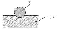
ここで、金属細線8の材料としては、金、銅、若しくはアルミニウムなどを用いることができる。また、金属細線8は、線径30〜100μmのものを用いる。線径が30μm未満であると、断面積が小さくなり、断線しやすく、生産上、取り扱いにくくなるとともに、タッチパネルに位置検出の誤差が発生しやすくなる。また、線径が100μmを超えると、透明電極12,22間のギャップが大きくなり入力が困難となる。 Here, as a material of the metal
上記金属細線8の上側及び下側透明絶縁基材11,21上への固着は、例えば、上側及び下側透明絶縁基材11,21の溶融固化により行なうことができる(図2参照)。具体的には、上側及び下側透明絶縁基材11,21上に金属細線8を配置した後、熱コテ、若しくは熱プレスなどの方法により加熱加圧を加え、上側及び下側透明絶縁基材11,21の表層部を軟化させ、冷却により金属細線8の一部を埋設した状態で固定する。ただし、下側電極部材2については、上記した下側電極部材2の下側透明絶縁基材21の材質が樹脂材料の場合に限定される。 The
また、上記金属細線8の固着は、外周表面が導電性のホットメルト材91により被覆された金属細線8を用い、当該ホットメルト材91の溶融固化により金属細線を上側及び下側透明絶縁基材11,21上に固着することもできる(図3参照)。具体的には、上側及び下側透明絶縁基材11,21上に導電性のホットメルト材91により被覆された金属細線8を配置した後、該金属細線8を加熱しながらプレスするなどの方法により加熱加圧を加え、ホットメルト材91を軟化させ、冷却によるホットメルト材91の接着力で金属細線8を固定する。上記導電性のホットメルト材91としては、クロロプレンなどの合成ゴム内に、金、銀、若しくはニッケル等の粒子を分散させた接着剤や、錫、鉛、若しくは錫と鉛の合金などを用いることができる。 Further, the
また、上記金属細線8の固着は、金属細線8と上側及び下側透明絶縁基材11,21との間に導電性ペースト92を介することにより行なうこともできる(図4参照)。導電性ペースト92としては、エポキシ樹脂、フェノール樹脂、アクリル樹脂、ウレタン樹脂、若しくはシリコン樹脂などの熱硬化性樹脂やポリアミド、又は、ポリエチレン、ポリスチレン、ポリエステル、ポリウレタン、エチレン−酢酸ビニール共重合体、若しくはエチレン−アクリル酸エチル共重合体などの熱可塑性樹脂中に導電性フィラーを含有させたものを用いる。導電性フィラーとしては、銀、金、銅、ニッケル、白金、若しくはパラジウムなどの導電性金属粉末のほか、核材としてアルミナ、若しくはガラスなどの無機絶縁体、又は、ポリエチレン、ポリスチレン、若しくはジビニルベンゼンなどの有機高分子などを用い、核材表面を金、若しくはニッケルなどの導電層で被覆したもの、カーボン、又はグラファイトなどが挙げられる。また、導電性フィラーは、フレーク状、球状、若しくは短繊維状などの形状のものを用いることができる。導電性ペースト92の金属細線8上及びその周囲の上側及び下側透明絶縁基材11,21上への被覆方法としては、スクリーン印刷、若しくはディスペンサーによる直接塗布などの方法を用いることができる。 The metal
また、上記金属細線8の固着は、金属細線8上及びその周囲の上側及び下側透明絶縁基材11,21上を接着剤93にて被覆することにより行なってもよい(図5参照)。具体的には、上側及び下側透明絶縁基材11,21上に金属細線8を配置した後、スクリーン印刷、若しくはディスペンサーによる直接塗布などの方法により金属細線8上及びその周囲の上側及び下側透明絶縁基材11,21上への被覆を行ない、上側及び下側透明絶縁基材11,21と接着剤93との間に金属細線8を挟み込んで固定する。接着剤93としては、エポキシ樹脂、アクリレート樹脂などを用いることができる。また、上記した上側及び下側透明絶縁基材11,21や導電性のホットメルト材91の溶融軟化、導電ペースト92の介在による固定手段をとる場合において、上記接着剤93による被覆を組み合わせることにより金属細線8の上側及び下側透明絶縁基材11,21上への固着力を向上させてもよい(図6〜図8参照)。この場合、金属細線8のみの場合には上側及び下側透明絶縁基材11,21に対して主として線接触であるのに対して、接着剤93として上記した導電性ペーストを用いれば、上側及び下側透明絶縁基材11,21に対しては面接触となり、金属細線8のみの場合よりも電気的接続抵抗が小さくなり、さらに導通性を向上させることができる。金属細線8を導電性ペーストにて固定する場合、金属細線8を上側及び下側透明絶縁基材11,21上に接続形成する際に、何らかのストレス、作業ミス等で金属細線8が断線しても、それを覆う導電性ペーストが補助導電材として作用する為、機能不良にならないという効果がある。 The metal
なお、上記した金属細線8の上側及び下側透明絶縁基材11,21上への固着は、上側及び下側バスバー13,14,23,24と上側及び下側引き回し回路15,16,25,26の全体で固着する必要はなく、導通と充分な固着が図れれば部分的でもよい。また、図2〜図8は上側及び下側引き回し回路15,16,25,26となる部分の断面図であるが、上側及び下側バスバー13,14,23,24の部分においては上側及び下側透明電極12,22が存在し、この上側及び下側透明電極12,22は上側及び下側透明絶縁基材11,21を溶融軟化させる場合には固着部分において上側及び下側透明絶縁基材11,21とともに変形する。 The above-mentioned
スペーサ3は、上側と下側の電極部材間で方形配置されるバスバーを絶縁しうる形態、たとえば図1に示すような枠形態などに形成される。スペーサ3の形成材としては、透明絶縁基材と同様の樹脂フィルム等のほか、アクリル系樹脂、エポキシ系樹脂、若しくはシリコーン系樹脂の如き適宜な樹脂を印刷又は塗布することによってスペーサ3を形成することができるが、一般に、上側電極部材1と下側電極部材2とを固定する枠形態の両面テープ、接着剤又は粘着剤からなる接着層と兼ねさせることが多い。接着剤又は粘着剤からなる接着層を形成する場合にはスクリーン印刷等が用いられる。 The
また、大判のタッチパネルを形成する場合、上側電極部材1と下側電極部材2の上側及び下側透明電極12,22間の空隙を確保するために、上側及び下側透明電極12,22のいずれか一方の表面にドット状スペーサ4を形成することもできる(図1参照)。ドット状スペーサ4としては、たとえばメラミンアクリレート樹脂、ウレタンアクリレート樹脂、エポキシアクリレート樹脂、メタアクリルアクリレート樹脂、アクリルアクリレート樹脂などのアクリレート樹脂、若しくはポリビニールアルコール樹脂などの透明な光硬化型樹脂をフォトプロセスで微細なドット状に形成して得ることができる。また、印刷法により微細なドットを多数形成して、スペーサとすることもできる。また、無機物や有機物からなる粒子の分散液を噴霧、又は塗布して乾燥することによってもスペーサを得ることができる。 When a large-sized touch panel is formed, any one of the upper and lower
本発明の第1実施形態の狭額縁タッチパネルは、上記した構成及び作用からなるので、次の効果が奏される。 Since the narrow frame touch panel according to the first embodiment of the present invention has the above-described configuration and operation, the following effects are achieved.
すなわち、本発明の第1実施形態の狭額縁タッチパネルは、上側及び下側バスバーと上側及び下側引き回し回路とを線径30〜100μmの金属細線にて形成したので、上側及び下側バスバー及び上側及び下側引き回し回路の形成時にパターニングが不要となり、無駄に材料を捨てずに済み、安価なタッチパネルが得られる。また、メッキ浴への全面浸漬する必要がないため透視入力する領域に汚れを生ずるおそれもなく、歩留まりがよい。 That is, in the narrow frame touch panel of the first embodiment of the present invention, the upper and lower bus bars and the upper and lower routing circuits are formed by thin metal wires having a wire diameter of 30 to 100 μm. In addition, patterning is not required when forming the lower routing circuit, and it is not necessary to waste material, and an inexpensive touch panel can be obtained. In addition, since it is not necessary to immerse the entire surface in the plating bath, there is no risk of contamination in the fluoroscopic input region, and the yield is good.
また、金属細線を用いることで、上側及び下側バスバーと上側及び下側引き回し回路は、充分な断面積をそれぞれ確保しながら、つまり、タッチパネルに位置検出の誤差が発生しないよう抵抗を小さく抑えながら、同時に幅を細く形成できる。したがって、タッチパネルの周縁部において上側及び下側バスバーと上側及び下側引き回し回路の形成面積をそれぞれ小さくすること、すなわち、狭額縁化を進めることができる。この場合、断面積の大きい、上側及び下側バスバー及び上側及び下側引き回し回路の形成に時間がかからず、生産効率に優れている。 In addition, by using fine metal wires, the upper and lower bus bars and the upper and lower routing circuits ensure a sufficient cross-sectional area respectively, that is, while suppressing the resistance small so that position detection errors do not occur on the touch panel. At the same time, the width can be narrowed. Therefore, it is possible to reduce the formation areas of the upper and lower bus bars and the upper and lower routing circuits at the peripheral edge of the touch panel, that is, to narrow the frame. In this case, it takes no time to form the upper and lower bus bars and the upper and lower routing circuits having a large cross-sectional area, and the production efficiency is excellent.
また、本発明の第1実施形態の狭額縁タッチパネルは、上側及び下側引き回し回路を金属細線にて形成するように構成することで、この金属細線を上側電極部材と下側電極部材との外側まで延設させて上側及び下側外部端子接続部とすることができ、フィルムコネクタを用いる必要がなくなる。したがって、上側電極部材と下側電極部材との間にフィルムコネクタを挿入して接続をするためのスペースを、タッチパネルの周縁に確保しなくても済み、より狭額縁化が可能である。 In addition, the narrow frame touch panel according to the first embodiment of the present invention is configured so that the upper and lower routing circuits are formed of metal thin wires, and the metal thin wires are arranged outside the upper electrode member and the lower electrode member. The upper and lower external terminal connecting portions can be extended to the end, eliminating the need to use a film connector. Therefore, it is not necessary to secure a space for inserting and connecting the film connector between the upper electrode member and the lower electrode member on the periphery of the touch panel, and the frame can be further narrowed.
また、本発明の第1実施形態の狭額縁タッチパネルは、フィルムコネクタを要しないため、タッチパネルの周縁部の全周に均一な接着強度が得られる。したがって、タッチパネルの高温試験などを行なっても、局所的に歪が生じて上側電極部材が波打つといった不具合が生じない。 Moreover, since the narrow frame touch panel of 1st Embodiment of this invention does not require a film connector, uniform adhesive strength is obtained in the perimeter of the peripheral part of a touch panel. Therefore, even if a high temperature test or the like of the touch panel is performed, there is no problem that the upper electrode member undulates due to local distortion.
次に、本発明の第2実施形態にかかる狭額縁タッチパネルは、入力領域や表示画面を広く取った狭額縁タッチパネルにおいて、金属細線の配置形状が第1実施形態と異なるものである。 Next, the narrow frame touch panel according to the second embodiment of the present invention is a narrow frame touch panel with a wide input area and display screen, and the arrangement shape of the thin metal wires is different from that of the first embodiment.
従来より、電子手帳やパソコンなどに使用されるタッチパネルとしてはアナログ抵抗膜方式のものがある。通常、図16に示されているように、透明絶縁基材511の下面の一部に透明電極512を有すると共に、透明電極512上に形成される一対のバスバー513,514、及び当該バスバー513,514と外部端子とを接続するように透明電極512以外の部分に形成される引き回し回路515,516をそれぞれ有する上側電極部材501と、透明絶縁基材521の上面の一部に透明電極522を有すると共に、透明電極522上に形成される一対のバスバー523,524、及び当該バスバー523,524と外部端子とを接続するように透明電極522以外の部分に形成される引き回し回路525,526をそれぞれ有する下側電極部材502とを、バスバー513,514,523,524が方形配置となるようにスペーサ3を介して対向させ、周縁部で接着している。また、引き回し回路515,516,525,526の他端はタッチパネルの一辺においてまとめられ、フィルムコネクタ505の端部と接続されている。 Conventionally, there is an analog resistive film type touch panel used for an electronic notebook or a personal computer. Normally, as shown in FIG. 16, a transparent electrode 512 is provided on a part of the lower surface of the transparent insulating
ところで、最近では上記のようなタッチパネルについて、製品の小型化及び画面の大型化のため、バスバー及び引き回し回路の配線がパネルの縁から僅かの狭額縁範囲に納まるように形成することが望まれている(特開2001−216090号公報参照)。 By the way, recently, in order to reduce the size of the product and the size of the screen, it is desired that the touch panel as described above be formed so that the wiring of the bus bar and the routing circuit is within a narrow frame range from the edge of the panel. (See Japanese Patent Laid-Open No. 2001-216090).
しかし、上記バスバー513,514,523,524及び引き回し回路515,516,525,526は、金、銀、銅、若しくはニッケルなどの金属あるいはカーボンなどの導電フィラーを樹脂バインダー中に分散させた導電性ペーストをスクリーン印刷してなるものなので、回路抵抗が大きく、狭額縁化のために線幅を細く形成すると回路抵抗はさらに大きくなる。しかも、線幅を細くすると、均一な膜厚での印刷が困難になり印刷の掠れが生ずる。この大きな回路抵抗や掠れは、タッチパネルの入力精度の低下を招く。因に、導電性ペーストは低抵抗のものを使用する工夫をしてきたが、現状は比抵抗値30×10−6Ω・cm程度が限界である。However, the bus bars 513, 514, 523, and 524 and the
また、従来技術は、バスバー513,514,523,524と外部端子との接続にフィルムコネクタ505を用い、且つバスバー513,514,523,524とフィルムコネクタ505との間には引き回し回路515,516,525,526が存在しているため、次のような問題も生じた。すなわち、フィルムコネクタ505と引き回し回路515,516,525,526とはタッチパネルの一辺においてまとめられて接続されていることが多く、この場合、同一面上において引き回し回路525とバスバー524とが並列に形成される。つまり、他辺と同様の額縁幅とするためには、各線幅をさらに細く形成する必要がある。これは上記した入力精度の低下をさらに増大させる。 In the prior art, a
また、引き回し回路515,516,525,526とフィルムコネクタ505との接続は従来より異方導電接着材を介して接着されるが、接着強度を確保するために、広い接着面積を必要とする。そのために、フィルムコネクタ505との接続部分の辺は、狭額縁にすることが困難となる。 Further, the connection between the routing
したがって、本発明の第2実施形態の目的は、上記の問題点を解決し、入力精度が高く、4辺とも狭額縁化が可能である狭額縁タッチパネルを提供することにある。 Accordingly, an object of the second embodiment of the present invention is to provide a narrow frame touch panel that solves the above-described problems and has high input accuracy and can be narrowed on all four sides.
以下に、図11〜図15、図22を参照しながら本発明の第2実施形態に係る狭額縁タッチパネルを詳細に説明する。 Hereinafter, a narrow frame touch panel according to the second embodiment of the present invention will be described in detail with reference to FIGS. 11 to 15 and FIG. 22.
図11及び図13に示されるタッチパネルは、上側透明絶縁基材11の下面の一部に上側透明電極12を有すると共に、上側透明電極12上に形成される一対の上側バスバー13,14を有する上側電極部材1と、下側透明絶縁基材21の上面の一部に下側透明電極22を有すると共に、下側透明電極22上に形成される一対の下側バスバー23,24を有する下側電極部材2とを、上側及び下側バスバー13,14,23,24が方形配置となるようにスペーサ3を介して対向させ、周縁部で接着しているアナログ抵抗膜方式のタッチパネルであり、本発明の第2実施形態の特徴として上記上側及び下側バスバー13,14,23,24のみ(言い換えれば、第2実施形態では引き回し回路は無く、上記上側及び下側バスバー13,14,23,24と上側及び下側外部端子接続部313,314,323,324と)を線径30〜100μmの金属細線113,114,223,224にて形成し、且つ当該金属細線113,114,223,224を上記上側電極部材1と上記下側電極部材2とを接着したものの外側まで上記上側及び下側バスバー13,14,23,24の一端から直接延設させて上側及び下側外部端子接続部313,314,323,324としたものである。一例として、下側電極部材2では、金属細線223,224を、図11の下側電極部材2の左下コーナー部分と右上コーナー部分のそれぞれから外側まで延設させて下側外部端子接続部323,324とするとともに、上側電極部材1では、2本の金属細線113,114を、図11の上側電極部材1の左下コーナー部分と右上コーナー部分のそれぞれから外側まで延設させて上側外部端子接続部313,314とするようにしている。なお、上記図11及び上記図13中、上側透明電極12及び上側バスバー13,14は上側透明絶縁基材11を透視して描かれている。 The touch panel shown in FIGS. 11 and 13 has an upper
なお、金属細線113,114,223,224の線径が30μm未満であると、断線しやすく、生産上、取り扱いにくくなる。また、金属細線113,114,223,224の線径が100μmを超えると、上側と下側透明電極12,22間のギャップが大きくなり入力が困難となる。 When the wire diameters of the
上記の比抵抗値20×10−6Ω・cm以下という条件を満足する金属細線113,114,223,224の材質としては、たとえば、金、銀、銅、ニッケル、錫、鉄等を用いることができる。金属細線113,114,223,224は、同一金属で構成されていても良いし、2種類以上の合金であっても良い。また金属細線113,114,223,224の周囲に1種類以上の金属層がメッキ等で被覆されていてもよい。また、金属細線113,114,223,224の断面形状も丸型、四角型、楕円型と特に限定されるものではなく、適宜適応できるような形状に設計すればよい。For example, gold, silver, copper, nickel, tin, iron, or the like is used as the material of the metal
また、本発明の第2実施形態の狭額縁タッチパネルにおいては、上記金属細線8,113,114,223,224の上側と下側透明絶縁基材11,21上への固定を、上側と下側透明絶縁基材11,21上の上記金属細線8,113,114,223,224とその周囲を導電性ペースト6で被覆することによって行なうとよい(図15及び図22参照)。なお、上記固定を確実にするには、厚み5μm以上の導電性ペースト6で被覆する。図22は、図15の詳細図であり、3Aは上側と下側透明電極12,22の絶縁確保のための絶縁層である。 In the narrow frame touch panel according to the second embodiment of the present invention, the upper side and the lower side of the metal
金属細線8,113,114,223,224を固定する際、金属細線113,114,223,224を上側と下側透明絶縁基材11,21上に配置してから導電性ペースト6を塗布しても良いし、あらかじめ金属細線8,113,114,223,224に導電性ペースト6を被覆してからこれを上側と下側透明絶縁基材11,21上に配置してもよい。 When fixing the
上記導電性ペースト6は、樹脂バインダー中に導電性フィラーが分散されているものである。導電性フィラーの材質としては、例えば、金、銀、銅、アルミニウム、ニッケル、錫、若しくはカーボン等がある。 The
樹脂バインダーとは、特定の材料同士を接合又は結合させる樹脂のことであり、本発明の上記第2実施形態の場合は、導電性フィラー同士の接合及び導電性フィラーを透明導電膜面上に接合させるための接合材のことである。樹脂バインダーとしては、アクリル系樹脂、ウレタン系樹脂、エポキシ系樹脂、又はシリコン系樹脂等の樹脂を用いることができ、硬化方法としては熱硬化、溶剤蒸発乾燥、又はUV硬化等により適宜硬化させて透明電極上に固着させる。特に、UV硬化の場合、塗布した端からほぼ同時に硬化が可能であるため、1)塗布が全て完了した後にオーブンに移して硬化させる必要がなく、作業が簡略化され、2)液垂れが起こる間がないので、線幅や厚みの寸法安定性に優れるといった効果を奏することができる。 The resin binder is a resin for bonding or bonding specific materials. In the case of the second embodiment of the present invention, bonding of conductive fillers and bonding of conductive fillers onto the transparent conductive film surface. It is a bonding material to make it. As the resin binder, a resin such as an acrylic resin, a urethane resin, an epoxy resin, or a silicon resin can be used. As a curing method, the resin binder is appropriately cured by thermal curing, solvent evaporation drying, UV curing, or the like. Fix on the transparent electrode. In particular, in the case of UV curing, since it is possible to cure almost simultaneously from the coated end, 1) it is not necessary to transfer to an oven after all the coating is completed, the work is simplified, and 2) dripping occurs. Since there is no gap, it is possible to achieve an effect that the dimensional stability of the line width and thickness is excellent.
また、導電性ペースト6で被覆して金属細線113,114,223,224を固定する場合、固定に必要な幅は50〜500μmが望ましい。幅が50μm未満となると、金属細線113,114,223,224と上側と下側透明電極12,22との接着性が弱くなり、上側と下側透明電極12,22から金属細線113,114,223,224が剥離してしまう可能性がある。幅が500μmを超えると、上側電極部材1と下側電極部材2の周縁部の接着力が弱くなり剥がれる恐れがあり、また狭額縁のメリットがなくなってしまう。 Further, when the metal
また、金属細線113,114,223,224の上記上側と下側バスバー13,14,23,24の一端からの延設部分である上側及び下側外部端子接続部313,314,323,324は、タッチパネルのコーナーにより近い箇所にすることが望ましい。延設部分をタッチパネルのコーナーに出来るだけ近く設計することにより、狭額縁化が可能で視認領域が広くなるからである。また、金属細線113,114,223,224の延設部分である上側及び下側外部端子接続部313,314,323,324は、タッチパネルのコーナー毎に配置されて外部端子と接続してもよいし(図14参照)、タッチパネルの対向する2コーナーに集約して配置されて外部端子と接続してもよい(図12参照)。外部端子の設計状況にあわせて金属細線113,114,223,224の延設箇所(上側及び下側外部端子接続部313,314,323,324の外部への延設配置箇所)を決定すればよい。なお、外部端子の設計状況とは別の観点からすれば、前者には金属細線同士の絶縁を確保できるという利点、後者には外部端子との接続リア数を減らせる、つまりタッチパネル以外の回路の省スペース化が可能になるという利点がある。 Further, the upper and lower external
上側電極部材1に用いられる上側透明絶縁基材11としては、ポリカーボネート系、ポリアミド系、ポリエーテルケトン系などのエンジニアリングプラスチック、アクリル系、ポリエチレンテレフタレート系、若しくはポリブチレンテレフタレート系などの透明フィルムなどの可撓性を有するものを用いることができる。さらに、上側電極部材1の上側透明絶縁基材11は、1枚のフィルムではなく複数枚のフィルムを重ね合わせた積層体とすることができる。なお、上側電極部材1の上側透明絶縁基材11の上側透明電極12を設けた面と反対の面にはハードコート層を形成することができる。ハードコート層としては、シロキサン系樹脂などの無機材料、あるいはアクリルエポキシ系、ウレタン系の熱硬化型樹脂やアクリレート系の光硬化型樹脂などの有機材料がある。ハードコート層の厚みは、1〜7×10⁻³mm程度が適当である。また、上側電極部材1の上側透明絶縁基材11には、上側透明電極12を設けた面と反対の面に光反射防止のためにノングレア処理を施すことができる。たとえば、上側透明電極12を設けた面と反対の面に凹凸加工を施したり、ハードコート層中に体質顔料やシリカ、アルミナなどの微粒子を混ぜたりするとよい。The upper transparent insulating
下側電極部材2に用いられる下側透明絶縁基材21としては、ソーダガラス、ホウケイ酸ガラス、若しくは強化ガラスなどのガラス板のほか、ポリカーボネート系、ポリアミド系、若しくはポリエーテルケトン系などのエンジニアリングプラスチック、又は、アクリル系、ポリエチレンテレフタレート系、ポリブチレンテレフタレート系などの透明樹脂板若しくは透明フィルムを用いることができる。下側電極部材2に用いる下側透明絶縁基材21は、透明フィルムと透明プラスチック板又はガラス板との積層品であってもよい。この場合はタッチパネル全体としての耐久性が向上するので好ましい。 As the lower transparent insulating
上側と下側透明電極12,22は、酸化錫、酸化インジウム、酸化アンチモン、酸化亜鉛、酸化カドミウム、インジウムチンオキサイド(ITO)などの金属酸化物膜、これらの金属酸化物を主体とする複合膜、又は金、銀、銅、錫、ニッケル、アルミニウム、パラジウムなどの金属膜によって、形成することができる。また、上側と下側透明電極12,22を2層以上の多層膜とすることができる。上側と下側透明電極12,22を構成するこれらの透明導電膜は真空蒸着、スパッタリング、イオンプレーティング、CVD法などで形成することができる。透明導電膜は、酸などでエッチング処理を行い、上側と下側透明電極12,22とする部分以外の不要な部分を除去する方法によってパターン化することができる。また、上側と下側透明導電膜上の上側と下側透明電極12,22とする部分以外を絶縁性被膜で覆うようにしてもよい。 The upper and lower
スペーサ3は、上側と下側透明電極12,22間のギャップを確保しうる形態、たとえば図11,図13に示すような枠形態などに形成される。スペーサ3の形成材としては、上側と下側透明絶縁基材と同様の樹脂フィルム等のほか、アクリル系樹脂、エポキシ系樹脂、若しくはシリコーン系樹脂の如き適宜な樹脂を印刷又は塗布したものを用いることができるが、一般に上側電極部材1と下側電極部材2とを周縁部で接着するための両面テープ、接着剤又は粘着剤からなる接着層と兼ねさせることが多い。なお、接着剤又は粘着剤からなる接着層を形成する場合には、確実に上下の絶縁を得るために、前述のとおり、透明導電膜のパターン化や絶縁性被膜の被覆が必要である。これに対して、両面テープの場合は、芯材を有しているため既に十分に絶縁性が確保されており、透明導電膜のパターン化や絶縁性被膜の被覆を行なわなくても構わない。すなわち、工程の省略や製造コストの抑制が可能である。 The
ところで、上側電極部材と下側電極部材の周縁部での接着に関し、本発明の第2実施形態の狭額縁タッチパネルは金属細線が引き回し回路を構成しないので、一方の電極部材のバスバーを有する辺に対向して貼り合わせる他方の電極部材の辺が常にフラットな面となる。したがって、狭額縁化しても接着性が劣化することがなく、タッチパネルの信頼性が増す。 By the way, regarding the bonding at the peripheral edge of the upper electrode member and the lower electrode member, the narrow frame touch panel of the second embodiment of the present invention does not constitute a circuit with a thin metal wire routed, so it is on the side having the bus bar of one electrode member. The side of the other electrode member that is bonded oppositely is always a flat surface. Therefore, even if the frame is narrowed, the adhesiveness is not deteriorated and the reliability of the touch panel is increased.
また、大判のタッチパネルを形成する場合、上側電極部材1と下側電極部材2の上側と下側透明電極12,22間の空隙を確保するために、上側と下側透明電極12,22のいずれか一方の表面にドット状スペーサ4を形成することもできる(図11,図13参照)。ドット状スペーサ4としては、たとえばメラミンアクリレート樹脂、ウレタンアクリレート樹脂、エポキシアクリレート樹脂、メタアクリルアクリレート樹脂、若しくはアクリルアクリレート樹脂などのアクリル系樹脂、又はポリビニールアルコール樹脂などの透明な光硬化型樹脂をフォトプロセスで微細なドット状に形成して得ることができる。また、印刷法により微細なドットを多数形成して、スペーサとすることもできる。また、無機物や有機物からなる粒子の分散液を噴霧、又は塗布して乾燥することによってもスペーサを得ることができる。 When a large-sized touch panel is formed, any one of the upper and lower
本発明の第2実施形態は、コンピュータに接続されたLCDやCRTなどの表示画面上に配置し、透視した表示画面に表示された指示に従って指やペンなどで上から押圧することにより、押圧箇所の表示画面中における位置をコンピュータに入力することができるアナログ抵抗膜方式のタッチパネルに関するものである。特に携帯性を重視した情報端末(PDA=パーソナルデジタルアシスタント)に使用できる。
また、本発明の第2実施形態の狭額縁タッチパネルは、上記した構成からなるので、次の効果が奏される。The second embodiment of the present invention is arranged on a display screen such as an LCD or CRT connected to a computer, and is pressed from above with a finger or a pen in accordance with instructions displayed on the fluoroscopic display screen. The present invention relates to an analog resistive touch panel that can input a position in the display screen to a computer. In particular, it can be used for an information terminal (PDA = personal digital assistant) that places importance on portability.
Moreover, since the narrow frame touch panel of 2nd Embodiment of this invention consists of an above-described structure, the following effect is show | played.
すなわち、本発明の第2実施形態の狭額縁タッチパネルは、バスバーのみ(言い換えれば、第2実施形態では引き回し回路は無く、上記上側及び下側バスバーと上側及び下側外部端子接続部と)を線径30〜100μmの金属細線にて形成し、且つ当該金属細線を上記上側電極部材と上記下側電極部材とを接着したものの外側まで上記バスバーの一端から直接延設させて上側及び下側外部端子接続部とするので、バスバーの線幅を細くしても回路抵抗の上昇を抑えることができ、入力精度の高いタッチパネルを提供できる。 That is, the narrow frame touch panel according to the second embodiment of the present invention has only a bus bar (in other words, there is no routing circuit in the second embodiment, and the upper and lower bus bars and the upper and lower external terminal connection portions) are wired. An upper and lower external terminal formed of a thin metal wire having a diameter of 30 to 100 μm and extending directly from one end of the bus bar to the outside of the metal wire bonded to the upper electrode member and the lower electrode member Since the connection portion is used, an increase in circuit resistance can be suppressed even if the line width of the bus bar is reduced, and a touch panel with high input accuracy can be provided.
また、本発明の第2実施形態の狭額縁タッチパネルは、引き回し回路が存在しないので、従来のように同一面上において引き回し回路とバスバーとが並列に形成されることがない。つまり、4辺の狭額縁化が、入力精度の低下させることなく可能となる。 Further, since the narrow frame touch panel according to the second embodiment of the present invention does not have a routing circuit, the routing circuit and the bus bar are not formed in parallel on the same surface as in the related art. That is, it is possible to narrow the four sides without reducing the input accuracy.
また、本発明の第2実施形態の狭額縁タッチパネルは、フィルムコネクタを用いないので、従来のようにフィルムコネクタの接着強度を確保するための広い接着面積を必要としない。したがって、4辺の狭額縁化が可能となる。 Moreover, since the narrow frame touch panel of the second embodiment of the present invention does not use a film connector, it does not require a wide bonding area for securing the bonding strength of the film connector as in the prior art. Therefore, it is possible to narrow the four sides.
また、本発明の第1実施形態及び第2実施形態によれば、金属細線及び導電性ペーストを用いることで、バスバー及び引き回し回路、又は、バスバーを従来よりも細かくすることが出来る為、それらを覆い絶縁を確保する為の枠状スペーサー(両面テープや粘着剤)も同時に細くすることが可能となり、有効操作エリアは、従来とおりのサイズを確保した上で、外形サイズを小さくすることが出来、装置全体の小型化が可能になる。 In addition, according to the first and second embodiments of the present invention, by using a fine metal wire and a conductive paste, the bus bar and the routing circuit, or the bus bar can be made finer than before, so that The frame-shaped spacer (double-sided tape and adhesive) to ensure covering insulation can be made thin at the same time, and the effective operation area can be reduced in size after securing the same size as before, The entire apparatus can be downsized.
なお、本発明は上記実施形態に限定されるものではなく、その他種々の態様で実施できる。 In addition, this invention is not limited to the said embodiment, It can implement with another various aspect.
例えば、上側電極部材1と下側電極部材2とのそれぞれから金属細線を外側まで延設させて上側及び下側外部端子接続部301,302,303,304とするようにしているが、これに限られるものではなく、本発明の第1実施形態の変形例にかかるタッチパネルとして、上側電極部材1と下側電極部材2とをまとめて1箇所で金属細線以外のもので外側まで延設させて上側及び下側外部端子接続部とするようにしてもよい。具体的には、図19〜図21に示されるように、上側電極部材1と下側電極部材2の引き回し回路の4本の金属細線をまとめて接続したフィルムコネクタ90を、図19の右辺の上側端部付近に配置するようにしてもよい。このようなフィルムコネクタ90はFPC(フレキシブル・プリンテッド・サーキット)により構成されてタッチパネルの取り出し部分を形成する場合には、以下のような利点がある。タッチパネルの駆動、ディスプレィの駆動、装置全体の駆動等を行っているメインボードに、可撓性のあるフィルムコネクタ90により、容易に接続・脱着することが可能となり、組み立て工数を減らすことができる。さらに、タッチパネル単体での電気検査(出荷時、評価時)が容易に出来、検査処理能力が向上する。また、標準FPCを使用することで、開発コストを低減することが可能となる。 For example, a thin metal wire is extended outward from each of the
金属細線8,113,114,223,224は、それぞれ、直線部150と屈曲部151とで構成されている。このうち屈曲部151は、環境温度変化により、引っ張り、収縮等のストレスがかかる為,それ以外の部分(直線部150)と比べてより強固に上側及び下側透明電極12,22に接続させる必要がある。その為、導電性ペースト93で金属細線8を覆うことにより被覆層を形成する際、導電性ペースト93の被覆層形成幅(図17参照:固定面である上側及び下側透明電極12,22の表面との接触幅)D2の屈曲部151における許容範囲は、直線部150における被覆層形成幅の許容範囲より下限値が大きくなるのが好ましい。The
導電性ペースト93で金属細線8を覆う際、導電性ペースト93の被覆層形成幅D2のバスバー部分における許容範囲は、それ以外の部分(第1実施形態の上側及び下側引き回し回路15,16,25,26、後述する第2実施形態の出力端部分)における被覆層形成幅D2の許容範囲より下限値が大きくなるのが好ましい。何故なら、バスバー部分の導電性ペースト93の被覆層形成幅D2が狭いと、金属細線8と透明電極(ITO膜等)11,12との接着性が不十分で、安定な接続抵抗が得られず、また、環境温度変化等による熱膨張差で、剥離してしまう可能性があるからである。これに対し、バスバー部分以外の部分は、透明導電膜を除去あるいは、透明導電膜上に絶縁膜をコーティングした部分に配置する為、下地膜との電気的な接続は不要であり、金属細線8のみで導通をとることになる。なお、バスバー部分以外の部分も、被覆層形成幅を狭くしすぎると、金属細線8が断線した場合に、先に述べたように導電性ペーストを補助導電材として機能させようとしても、導通確保が出来なくなる。When covering the metal
また、上側透明電極12と金属細線8との接続は、入力時や環境温度変化により、引っ張り、収縮、たわみ等のストレスがかかる為、下側透明電極22と金属細線8との接続よりも、より強固に接続させる必要がある。その為、導電性ペースト93で金属細線8を覆う際、上側透明電極12での導電性ペースト93の被覆層形成幅D2の許容範囲は、下側透明電極22での導電性ペースト93の被覆層形成幅D2の許容範囲より下限値が大きくなるのが好ましい。In addition, the connection between the upper
この結果、例えば、以下の表1のように導電性ペースト93の被覆層形成幅D2を構成することが好ましい。As a result, for example, it is preferable to form the coating layer formation width D2 of the

このようにすることで、金属細線8と上側及び下側透明電極12,22との接続面積を確保出来、引っ張り、収縮のストレスに強くなる。例えば直線部150を比較的狭い幅で形成したわかりやすい形で敢えて図示すると、図18のように屈曲部151にランドが形成されたようになる。なお、直線部150の幅を屈曲部151に合わせて太くすることもできる。 By doing in this way, the connection area of the metal
さらに、鋭意検討した結果、本発明の第2実施形態に用いる金属細線113,114,223,224としては、比抵抗値20×10−6Ω・cm以下であれば上記線径30〜100μmで十分に低抵抗化することができる。ここで、比抵抗値20×10−6Ω・cm以下とする理由は、以下のとおりである。すなわち、スクリーン印刷で十分に回路形成パターンを形成するための限界印刷において、幅は0.5mmで厚みは5μ程度になる。その場合、導電性ペーストの一般的な比抵抗値が9×10⁻⁵Ω・cmであるため、回路抵抗は0.35Ω/cmとなる。それに対し、直径30μmの金属細線を用いる場合、スクリーン印刷と同等の回路抵抗値を得るためには、本発明に用いる金属細線8,113,114,223,224の比抵抗値は約25×10−6Ω・cmとなるため、金属細線の比抵抗値が20×10−6Ω・cm以下のものを選択することにより、スクリーン印刷で回路形成するよりも、さらに低抵抗で狭額縁な回路形成が可能となるからである。Furthermore, as a result of intensive studies, the
なお、上記金属細線8,113,114,223,224の固定手段としては、上記したもの以外の方法を用いることもできる。例えば、透明絶縁基材11,21の溶融固化により行なうことができる。また、金属細線113,114,223,224上及びその周囲の上側と下側透明絶縁基材11,21上を接着剤にて被覆することにより行なってもよい。しかし、上記した上側と下側透明絶縁基材11,21上の上記金属細線113,114,223,224とその周囲を導電性ペーストで被覆する手段が、透明電極12,22を加熱加圧して劣化させる恐れがない点、透明電極12,22と金属細線113,114,223,224との導電安定性がある点で最も好ましい。 In addition, as a fixing means for the metal
また、導電性ペースト6としては、比抵抗値1×10⁻⁴Ω・cm以下のものを用いることが望ましい。従来の回路形成用の導電性ペーストであればさらに低抵抗の必要があるが、本発明の第2実施形態では、金属細線8,113,114,223,224が上側と下側バスバー13、14、23、24の核になっており、当該金属細線8,113,114,223,224と透明電極12,22間との導通が確保できればいいので、導電性ペースト6の選択範囲の上限が比抵抗値1×10⁻⁴Ω・cmまで広がり、接着性頼性等も十分考慮して選定することができる。ただし、あらかじめ金属細線8,113,114,223,224に導電性ペースト6を被覆してからこれを上側及び下側透明絶縁基材11,21上に配置する場合、あるいは断面形状が丸型である場合、又は上側及び下側透明電極12,22との接触面積が小さい金属細線を上側及び下側透明絶縁基材11,21上に配置してから導電性ペースト6を塗布する場合には、導電性ペースト6の抵抗が問題になる。導電性ペースト6の比抵抗が1×10⁻⁴Ω・cmを超えると、金属細線と透明電極12,22間の抵抗上昇が無視できなくなり、ペン入力時の入力精度が低下する。Moreover, as the
なお、上記様々な実施形態のうちの任意の実施形態を適宜組み合わせることにより、それぞれの有する効果を奏するようにすることができる。 It is to be noted that, by appropriately combining arbitrary embodiments of the various embodiments described above, the effects possessed by them can be produced.
本発明は、添付図面を参照しながら好ましい実施形態に関連して充分に記載されているが、この技術の熟練した人々にとっては種々の変形や修正は明白である。そのような変形や修正は、添付した請求の範囲による本発明の範囲から外れない限りにおいて、その中に含まれると理解されるべきである。 Although the present invention has been fully described in connection with preferred embodiments with reference to the accompanying drawings, various variations and modifications will be apparent to those skilled in the art. Such changes and modifications are to be understood as being included therein, so long as they do not depart from the scope of the present invention according to the appended claims.
縦65mm、横86mm、厚み125μmのポリエステル樹脂フィルムを下側透明絶縁基材として用い、その上面に厚み15nmのITO膜をスパッタリングにて形成し、ITO膜の周縁部分を除去して下側透明電極とした。次いで、下側透明電極の平行な二辺の下側バスバー及び下側透明電極以外の部分にてこの下側バスバーに接続する下側引き回し回路となるように、金からなる線径50μmの金属細線を2本、一端を下側透明絶縁基材の外側に15mm延長して配置した。さらに、金属細線を被覆するようにディスペンサーで導電性ペーストを塗布して、150μmの幅で金属細線を下側透明絶縁基材に固定し、下側透明絶縁基材の端より幅0.5mmを額縁部分とする下側電極部材を得た。 A polyester resin film having a length of 65 mm, a width of 86 mm, and a thickness of 125 μm is used as a lower transparent insulating base material. An ITO film having a thickness of 15 nm is formed on the upper surface by sputtering, and the peripheral portion of the ITO film is removed to form a lower transparent electrode. It was. Next, a metal thin wire having a wire diameter of 50 μm made of gold so as to form a lower routing circuit connected to the lower bus bar at the portions other than the lower bus bar and the lower transparent electrode on two parallel sides of the lower transparent electrode. And one end extended 15 mm outside the lower transparent insulating substrate. Furthermore, the conductive paste is applied with a dispenser so as to cover the fine metal wires, and the fine metal wires are fixed to the lower transparent insulating base material with a width of 150 μm, and the width of 0.5 mm from the end of the lower transparent insulating base material. A lower electrode member having a frame portion was obtained.
また、縦横が下側電極部材の透明絶縁基材と同寸法で、厚み188μmのポリエステル樹脂フィルムを上側電極部材の上側透明絶縁基材として用い、下側電極部材と同様にして上側電極部材を得た。最後に、両電極部材を電極間に空気層を介して対向配置させ、両者を周縁部において両面テープにて接着し、狭額縁タッチパネルを得た。 Further, a polyester resin film having a length and width of the same dimensions as the transparent insulating substrate of the lower electrode member and a thickness of 188 μm is used as the upper transparent insulating substrate of the upper electrode member, and an upper electrode member is obtained in the same manner as the lower electrode member. It was. Finally, both electrode members were placed opposite to each other via an air layer between the electrodes, and both were bonded with a double-sided tape at the peripheral edge portion to obtain a narrow frame touch panel.
外周表面が錫からなる導電性のホットメルト材により被覆された金属細線を用い、これを加熱することによるホットメルト材の溶融固化により金属細線を上側と下側の透明絶縁基材上にそれぞれ固定したこと以外、実施例1と同様とした。 Using fine metal wires coated with a conductive hot melt material consisting of tin on the outer peripheral surface, the fine metal wires are fixed on the upper and lower transparent insulating substrates by heating and solidifying the hot melt material. Except that, it was the same as Example 1.
上側と下側の透明絶縁基材上にディスペンサーにより銀ペーストをそれぞれ塗布し、これを介して金属細線を上側と下側の透明絶縁基材上にそれぞれ固定したこと以外、実施例1と同様とした。 The same as in Example 1, except that the silver paste was applied to the upper and lower transparent insulating substrates by a dispenser, and the fine metal wires were respectively fixed on the upper and lower transparent insulating substrates through this. did.
金属細線を上側と下側の透明絶縁基材上にそれぞれ固定した後、さらに金属細線上及びその周囲の上側と下側の透明絶縁基材上を銀ペーストを用いてディスペンサーにより塗布してそれぞれ被覆したこと以外、実施例1と同様とした。 After fixing the thin metal wires on the upper and lower transparent insulating substrates, respectively, and further coating the upper and lower transparent insulating substrates on and around the fine metal wires using a silver paste with a dispenser. Except that, it was the same as Example 1.
縦85mm、横60mm、厚み188μmのポリエステル樹脂フィルムを下側透明絶縁基材として用い、その上面に厚み10nmのITO膜をスパッタリングにて全面形成し、ITO膜の短辺部分(0.5mm幅)を除去してその他の箇所を下側透明電極とした。次いで、下側透明絶縁基材の長辺について、その端から0.2mm内側の位置に線径80μmの銅線に厚み10μmの錫メッキをしてなる線径100μmの金属細線(比抵抗値1.7×10⁻⁴Ω・cm)を張力をかけた状態でそれぞれ配置し、下側透明絶縁基材上の金属細線を下側バスバーとした。次に、張力をかけた状態の下側バスバーとその周囲の上に、樹脂バインダー中に銀の導電フィラーを含有した導電性ペースト(東洋紡製「DW250H−57」:比抵抗値3.5×10⁻⁵Ω・cm)を内径300μmの針先のディスペンサーを用いて厚み15μmとなるように塗布し、80℃30分乾燥を行うことにより金属細線を固定した。次いで、金属細線のうち一方はバスバーの端より切り落とし、他端は下側バスバーより8mm先で切り落として下側電極部材を得た。下側バスバーの固定に要した幅は350μm、回路抵抗は0.09Ω/cmと低いものであった。A polyester resin film having a length of 85 mm, a width of 60 mm, and a thickness of 188 μm was used as the lower transparent insulating substrate, and an ITO film having a thickness of 10 nm was formed on the entire surface by sputtering, and the short side portion (0.5 mm width) of the ITO film. The other part was made into the lower transparent electrode. Next, with respect to the long side of the lower transparent insulating base material, a thin metal wire having a wire diameter of 100 μm (specific resistance value 1) formed by tin plating with a thickness of 10 μm on a copper wire with a wire diameter of 80 μm at a position 0.2 mm inside from the end .7 × 10−4 Ω · cm) was placed under tension, and the thin metal wire on the lower transparent insulating substrate was used as the lower bus bar. Next, a conductive paste containing a silver conductive filler in a resin binder (“DW250H-57” manufactured by Toyobo: specific resistance value 3.5 × 10 10) on the lower bus bar and its periphery under tension.−5 Ω · cm) was applied to a thickness of 15 μm using a needle tip dispenser having an inner diameter of 300 μm, and dried at 80 ° C. for 30 minutes to fix the fine metal wires. Next, one of the metal thin wires was cut off from the end of the bus bar, and the other end was cut off 8 mm ahead of the lower bus bar to obtain a lower electrode member. The width required for fixing the lower bus bar was 350 μm, and the circuit resistance was as low as 0.09 Ω / cm.
他方、縦横が下側電極部材の下側透明絶縁基材と同寸法で、厚み188μmのポリエステル樹脂フィルムを上側電極部材の上側透明絶縁基材として用い、上側透明絶縁基材の短辺に上側バスバーを形成する以外は下側電極部材と同様にして、上側電極部材を得た。 On the other hand, a polyester resin film having the same vertical and horizontal dimensions as the lower transparent insulating base material of the lower electrode member and a thickness of 188 μm is used as the upper transparent insulating base material of the upper electrode member. An upper electrode member was obtained in the same manner as the lower electrode member, except that was formed.
上側と下側透明電極上に形成される一対の上側と下側バスバーを有する上記下側電極部材及び上記上側電極部材を、上側と下側バスバーが方形配置となるように且つ金属細線の上記延設部分である上側及び下側外部端子接続部がタッチパネルのコーナー毎に配置されるように、上側と下側透明電極間に空気層を介して対向配置させ、両者を周縁部で0.5mm幅の両面テープにて接着し、狭額縁タッチパネルを得た。 The lower electrode member having a pair of upper and lower bus bars formed on the upper and lower transparent electrodes and the upper electrode member are arranged so that the upper and lower bus bars are in a square arrangement and the metal thin wires are extended. The upper and lower external terminal connection portions, which are provided portions, are arranged to face each other via an air layer between the upper and lower transparent electrodes so that they are arranged at each corner of the touch panel. A double-sided adhesive tape was used to obtain a narrow frame touch panel.
金属細線の延設部分である上側及び下側外部端子接続部が、タッチパネルの対向する2コーナーに集約して配置されている以外は、実施例5と同様とした。 Example 5 was the same as Example 5 except that the upper and lower external terminal connection portions, which are the extended portions of the fine metal wires, were arranged in two opposing corners of the touch panel.
1 上側電極部材
11 上側透明絶縁基材
12 上側透明電極
13 上側バスバー
14 上側バスバー
15 引き回し回路
16 引き回し回路
2 下側電極部材
21 下側透明絶縁基材
22 下側透明電極
23 下側バスバー
24 下側バスバー
25 引き回し回路
26 引き回し回路
3 スペーサ
4 ドット状スペーサ
301 上側外部端子接続部
302 上側外部端子接続部
303 下側外部端子接続部
304 下側外部端子接続部
8 金属細線
91 ホットメルト材
92 導電性ペースト
93 接着剤(導電性ペーストを含む)
401 上側電極部材
411 透明絶縁基材
412 透明電極
413 バスバー
414 バスバー
415 引き回し回路
416 引き回し回路
402 下側電極部材
421 透明絶縁基材
422 透明電極
423 バスバー
424 バスバー
425 引き回し回路
426 引き回し回路
403 スペーサ
407 フィルムコネクタ
404 分圧出力端
405 分圧出力端
113 金属細線
114 金属細線
223 金属細線
224 金属細線
313 上側外部端子接続部
314 上側外部端子接続部
323 下側外部端子接続部
324 下側外部端子接続部
6 導電性ペースト
501 上側電極部材
511 透明絶縁基材
512 透明電極
513 バスバー
514 バスバー
515 引き回し回路
516 引き回し回路
502 下側電極部材
521 透明絶縁基材
522 透明電極
523 バスバー
524 バスバー
525 引き回し回路
526 引き回し回路
503 スペーサ
504 ドット状スペーサ
505 フィルムコネクタ
150 直線部
151 屈曲部
90 フィルムコネクタ
3A 絶縁層DESCRIPTION OF
401 Upper electrode member 411 Transparent insulating
Claims (9)
Translated fromJapanese可撓性を有する上側透明絶縁基材の下面の一部に上側透明電極を有すると共に、上記上側透明電極の平行な2辺に一対の上側バスバーと、上記上側透明電極以外の部分に上記上側バスバーと接続される上側外部端子接続部とをそれぞれ有する上側電極部材とを備えて、
上記下側電極部材と上記上側電極部材とを、上記上側バスバーと上記下側バスバーとが方形配置となるように絶縁性のスペーサを介して対向させ、周縁部において接着しているアナログ抵抗膜方式のタッチパネルにおいて、
上記下側バスバーを線径30〜100μmの金属細線にて形成するとともに、上記上側バスバーを線径30〜100μmの金属細線にて形成している狭額縁タッチパネル。A lower transparent electrode is provided on a part of the upper surface of the lower transparent insulating substrate, and a pair of lower bus bars are provided on two parallel sides of the lower transparent electrode, and the lower side is provided on a portion other than the lower transparent electrode. Lower electrode members each having a lower external terminal connection portion connected to the bus bar;
The upper transparent electrode has an upper transparent electrode on a part of the lower surface of the upper transparent insulating substrate having flexibility, a pair of upper bus bars on two parallel sides of the upper transparent electrode, and the upper bus bar on a portion other than the upper transparent electrode. And an upper electrode member each having an upper external terminal connection portion connected to the
An analog resistance film system in which the lower electrode member and the upper electrode member are opposed to each other through an insulating spacer so that the upper bus bar and the lower bus bar are in a square arrangement, and are bonded at the peripheral portion. In the touch panel of
A narrow frame touch panel in which the lower bus bar is formed of a thin metal wire having a wire diameter of 30 to 100 μm and the upper bus bar is formed of a thin metal wire having a wire diameter of 30 to 100 μm.
Priority Applications (1)
| Application Number | Priority Date | Filing Date | Title |
|---|---|---|---|
| JP2003412052AJP4346426B2 (en) | 2002-12-10 | 2003-12-10 | Narrow frame touch panel |
Applications Claiming Priority (3)
| Application Number | Priority Date | Filing Date | Title |
|---|---|---|---|
| JP2002357424 | 2002-12-10 | ||
| JP2003339264 | 2003-09-30 | ||
| JP2003412052AJP4346426B2 (en) | 2002-12-10 | 2003-12-10 | Narrow frame touch panel |
Publications (2)
| Publication Number | Publication Date |
|---|---|
| JP2005128993A JP2005128993A (en) | 2005-05-19 |
| JP4346426B2true JP4346426B2 (en) | 2009-10-21 |
Family
ID=32716283
Family Applications (1)
| Application Number | Title | Priority Date | Filing Date |
|---|---|---|---|
| JP2003412052AExpired - Fee RelatedJP4346426B2 (en) | 2002-12-10 | 2003-12-10 | Narrow frame touch panel |
Country Status (7)
| Country | Link |
|---|---|
| US (1) | US7499038B2 (en) |
| EP (1) | EP1571537A4 (en) |
| JP (1) | JP4346426B2 (en) |
| KR (1) | KR20050085413A (en) |
| CN (1) | CN100359447C (en) |
| TW (1) | TW200417929A (en) |
| WO (1) | WO2004061640A1 (en) |
Families Citing this family (53)
| Publication number | Priority date | Publication date | Assignee | Title |
|---|---|---|---|---|
| US7808479B1 (en) | 2003-09-02 | 2010-10-05 | Apple Inc. | Ambidextrous mouse |
| US7656393B2 (en) | 2005-03-04 | 2010-02-02 | Apple Inc. | Electronic device having display and surrounding touch sensitive bezel for user interface and control |
| US11275405B2 (en) | 2005-03-04 | 2022-03-15 | Apple Inc. | Multi-functional hand-held device |
| US20060001655A1 (en)* | 2004-07-01 | 2006-01-05 | Koji Tanabe | Light-transmitting touch panel and detection device |
| JP4772460B2 (en)* | 2005-11-10 | 2011-09-14 | 宸鴻光電科技股▲分▼有限公司 | Contact control panel wiring structure |
| JP4506742B2 (en)* | 2006-01-27 | 2010-07-21 | エプソンイメージングデバイス株式会社 | Touch panel, electro-optical device and electronic apparatus |
| EP2141566B1 (en)* | 2006-03-03 | 2021-01-27 | Apple Inc. | Electronic device having display and surrounding touch sensitive surfaces for user interface and control |
| CN102981678B (en)* | 2006-06-09 | 2015-07-22 | 苹果公司 | Touch screen liquid crystal display |
| US8022935B2 (en) | 2006-07-06 | 2011-09-20 | Apple Inc. | Capacitance sensing electrode with integrated I/O mechanism |
| KR101330697B1 (en) | 2006-12-21 | 2013-11-18 | 삼성디스플레이 주식회사 | Display device |
| JP2008305036A (en)* | 2007-06-06 | 2008-12-18 | Hitachi Displays Ltd | Display device with touch panel |
| JP5186496B2 (en)* | 2007-06-28 | 2013-04-17 | 京セラ株式会社 | Touch panel and touch panel display device |
| JP4915954B2 (en)* | 2007-11-27 | 2012-04-11 | グンゼ株式会社 | Touch panel and touch panel device using the touch panel |
| WO2009078391A1 (en)* | 2007-12-14 | 2009-06-25 | Kyocera Corporation | Touch panel and touch panel display device |
| JP5172385B2 (en)* | 2008-02-25 | 2013-03-27 | 株式会社ワコム | INPUT DEVICE WITH DISPLAY FUNCTION AND PORTABLE ELECTRONIC DEVICE |
| JP2009259203A (en)* | 2008-03-25 | 2009-11-05 | Epson Imaging Devices Corp | Capacitive input device, display device with input function, and electronic apparatus |
| CN102047207B (en) | 2008-05-29 | 2013-10-02 | 日本写真印刷株式会社 | Protection panel having touch input function |
| CN102089735A (en)* | 2008-08-07 | 2011-06-08 | 夏普株式会社 | Touch panel, display, and electronic device |
| EP2169520A3 (en)* | 2008-09-26 | 2011-07-13 | Tovis Co. Ltd. | Touch panel using tempered glass |
| JP5331437B2 (en)* | 2008-10-09 | 2013-10-30 | 株式会社ジャパンディスプレイ | Liquid crystal display |
| TWI398809B (en)* | 2009-09-11 | 2013-06-11 | Wintek Corp | Capacitive touch panel |
| KR101032021B1 (en)* | 2009-04-20 | 2011-05-02 | 에이디반도체(주) | Resistive touch screen recognizes touch coordinates through capacitor charging time |
| TWM367375U (en)* | 2009-05-05 | 2009-10-21 | Minlad Invest Ltd | Resistive touch panel |
| JP5396335B2 (en) | 2009-05-28 | 2014-01-22 | 株式会社半導体エネルギー研究所 | Touch panel |
| CN101943965B (en)* | 2009-07-08 | 2013-09-18 | 群康科技(深圳)有限公司 | Touch screen and electronic device therewith |
| US20110012845A1 (en)* | 2009-07-20 | 2011-01-20 | Rothkopf Fletcher R | Touch sensor structures for displays |
| CN101989135A (en)* | 2009-08-07 | 2011-03-23 | 希姆通信息技术(上海)有限公司 | Configuration method of touch screen circuit |
| US8654524B2 (en) | 2009-08-17 | 2014-02-18 | Apple Inc. | Housing as an I/O device |
| CN101995988B (en)* | 2009-08-19 | 2012-08-15 | 群康科技(深圳)有限公司 | Touch screen |
| TWI426426B (en) | 2009-12-31 | 2014-02-11 | Au Optronics Corp | Touch-sensing display module and touch-sensing module thereof |
| CN101763204B (en)* | 2010-01-18 | 2012-10-31 | 友达光电股份有限公司 | Touch display device and touch module included therein |
| CN201732354U (en)* | 2010-04-11 | 2011-02-02 | 宸鸿科技(厦门)有限公司 | Stack structure with enhanced touch panel bonding strength |
| KR101706232B1 (en) | 2010-06-29 | 2017-02-15 | 엘지디스플레이 주식회사 | Touch panel |
| KR20110125155A (en)* | 2010-08-30 | 2011-11-18 | 삼성전기주식회사 | touch screen |
| KR20120030832A (en)* | 2010-09-20 | 2012-03-29 | 삼성전기주식회사 | Touch screen and method of manufacturing the same |
| KR20120038823A (en)* | 2010-10-14 | 2012-04-24 | 삼성전기주식회사 | Touch screen |
| CN102478992B (en)* | 2010-11-26 | 2015-02-25 | 群康科技(深圳)有限公司 | touch screen |
| US8520380B2 (en)* | 2010-12-21 | 2013-08-27 | Luminous Optical Technology Co., Ltd. | Frame of touch panel |
| US9122088B2 (en)* | 2011-03-31 | 2015-09-01 | Nissha Printing Co., Ltd. | Capacitance type touch screen |
| JP5569891B2 (en)* | 2011-11-17 | 2014-08-13 | グンゼ株式会社 | Touch panel and manufacturing method thereof |
| JP5876351B2 (en)* | 2012-03-29 | 2016-03-02 | 三菱製紙株式会社 | Light transmissive electrode |
| CN103389818A (en)* | 2012-05-10 | 2013-11-13 | 介面光电股份有限公司 | touch panel |
| TW201421304A (en)* | 2012-11-22 | 2014-06-01 | Ibm | Method for repairing a touch panel, repairing component, and touch panel |
| CN103870080A (en)* | 2012-12-07 | 2014-06-18 | 联胜(中国)科技有限公司 | Touch panel and touch display module |
| KR20140084880A (en) | 2012-12-27 | 2014-07-07 | 삼성전기주식회사 | Touch Panel |
| KR101613773B1 (en) | 2013-11-04 | 2016-04-19 | 주식회사 동부하이텍 | Touch Panel and Method Manufacturing the Same |
| CN105072217B (en)* | 2015-07-17 | 2018-05-22 | 广东欧珀移动通信有限公司 | The operation circuit of mobile terminal, method and system |
| US10324620B2 (en) | 2016-09-06 | 2019-06-18 | Apple Inc. | Processing capacitive touch gestures implemented on an electronic device |
| US20200016867A1 (en)* | 2016-11-18 | 2020-01-16 | Unist(Ulsan National Institute Of Science And Technology) | Silver nanowire film and manufacturing method therefore, and thuch screen panel and manufacturing method therefor |
| KR102054934B1 (en)* | 2018-05-29 | 2019-12-12 | 일진디스플레이(주) | Touch Panel With Transparent Flexible Electrodes And Manufacturing Methods Thereof |
| CN111782086B (en)* | 2020-07-10 | 2022-05-06 | 业成科技(成都)有限公司 | Touch panel and manufacturing method thereof |
| KR102815227B1 (en)* | 2020-08-04 | 2025-06-02 | 삼성전자주식회사 | Electronic device with wireless charging |
| KR102711954B1 (en)* | 2020-12-11 | 2024-10-02 | (주)아이테드 | Hybrid busbar and heating module including the same |
Family Cites Families (16)
| Publication number | Priority date | Publication date | Assignee | Title |
|---|---|---|---|---|
| JPS5933069Y2 (en)* | 1982-07-03 | 1984-09-14 | アルプス電気株式会社 | input device |
| US4625075A (en)* | 1984-09-25 | 1986-11-25 | Sierracin Corporation | Patterned conductive ink touch panel |
| JPS63269218A (en) | 1987-04-27 | 1988-11-07 | Shin Etsu Polymer Co Ltd | Error detecting circuit for coordinate input device |
| JPH0178326U (en)* | 1987-11-10 | 1989-05-26 | ||
| JPH01281622A (en) | 1988-05-09 | 1989-11-13 | Daicel Chem Ind Ltd | Transparent touch type input device |
| JPH036867A (en)* | 1989-06-05 | 1991-01-14 | Mitsubishi Electric Corp | Electrode structure of photovoltaic device, forming method, and apparatus for manufacture thereof |
| JPH0378326A (en) | 1989-08-22 | 1991-04-03 | Pioneer Electron Corp | Audio system provided with reception function for roadside band broadcasting |
| GB9406702D0 (en)* | 1994-04-05 | 1994-05-25 | Binstead Ronald P | Multiple input proximity detector and touchpad system |
| JPH0936395A (en) | 1995-07-17 | 1997-02-07 | Canon Inc | Photovoltaic device and method of forming the same |
| US6597946B2 (en)* | 1998-11-09 | 2003-07-22 | Transpharma Ltd. | Electronic card for transdermal drug delivery and analyte extraction |
| JP4441102B2 (en) | 1999-11-22 | 2010-03-31 | キヤノン株式会社 | Photovoltaic element and manufacturing method thereof |
| JP4104800B2 (en)* | 1999-12-08 | 2008-06-18 | 三菱電機株式会社 | Liquid crystal display device and TFT panel |
| JP2001216090A (en) | 2000-01-31 | 2001-08-10 | Nissha Printing Co Ltd | Narrow frame touch panel |
| US6727895B2 (en)* | 2000-02-02 | 2004-04-27 | 3M Innovative Properties Company | Touch screen panel with integral wiring traces |
| TW508562B (en)* | 2001-01-10 | 2002-11-01 | Atouch Co Ltd | A contact structure of touch panel |
| JP2002287902A (en)* | 2001-01-17 | 2002-10-04 | Seiko Epson Corp | Touch panel and electronic equipment |
- 2003
- 2003-12-10JPJP2003412052Apatent/JP4346426B2/ennot_activeExpired - Fee Related
- 2003-12-10WOPCT/JP2003/015768patent/WO2004061640A1/enactiveApplication Filing
- 2003-12-10TWTW092134858Apatent/TW200417929A/enunknown
- 2003-12-10EPEP03814544Apatent/EP1571537A4/ennot_activeWithdrawn
- 2003-12-10KRKR1020057010278Apatent/KR20050085413A/ennot_activeAbandoned
- 2003-12-10USUS10/538,509patent/US7499038B2/ennot_activeExpired - Fee Related
- 2003-12-10CNCNB2003801053044Apatent/CN100359447C/ennot_activeExpired - Fee Related
Also Published As
| Publication number | Publication date |
|---|---|
| TW200417929A (en) | 2004-09-16 |
| CN100359447C (en) | 2008-01-02 |
| US7499038B2 (en) | 2009-03-03 |
| CN1720499A (en) | 2006-01-11 |
| EP1571537A1 (en) | 2005-09-07 |
| WO2004061640A1 (en) | 2004-07-22 |
| KR20050085413A (en) | 2005-08-29 |
| EP1571537A4 (en) | 2006-09-27 |
| US20060132465A1 (en) | 2006-06-22 |
| JP2005128993A (en) | 2005-05-19 |
Similar Documents
| Publication | Publication Date | Title |
|---|---|---|
| JP4346426B2 (en) | Narrow frame touch panel | |
| EP2871558B1 (en) | Touch window and touch device including the same | |
| JP4794392B2 (en) | Touch panel with curved surface and method for manufacturing the same | |
| KR101153389B1 (en) | Touch screen panel and touch screen assembly including the same | |
| TWI610600B (en) | Wiring body and wiring board | |
| US10091872B2 (en) | Touch window and display including the same | |
| US8350727B2 (en) | Touch panel and electronic device including the same | |
| WO2009104461A1 (en) | Touch panel and method for manufacturing the same | |
| JPH08203382A (en) | Analog transparent touch panel and manufacturing method thereof | |
| JP2013122745A (en) | Touch panel and manufacturing method thereof | |
| CN105278737A (en) | Touch panel | |
| US20070139393A1 (en) | Touch Panel | |
| JP4356416B2 (en) | Touch panel | |
| US20200064971A1 (en) | Wiring body assembly, wiring board, and touch sensor | |
| JP4550251B2 (en) | Narrow frame touch panel | |
| JP2005071123A (en) | Touch panel and electronic device using the same | |
| CN109002206B (en) | Touch structure, display device and preparation method of touch structure | |
| JPH10283117A (en) | Touch panel | |
| JP5618083B2 (en) | Method for manufacturing touch panel member | |
| KR100891712B1 (en) | Touch panel and its manufacturing method | |
| JP2004240662A (en) | Four-side narrow frame touch panel | |
| JPH1091345A (en) | Touch panel | |
| JP4390638B2 (en) | Narrow frame touch panel | |
| TWI897032B (en) | Variable resistor and method for manufacturing the same | |
| JP2018110153A (en) | Wiring assembly, wiring board, and touch sensor |
Legal Events
| Date | Code | Title | Description |
|---|---|---|---|
| A621 | Written request for application examination | Free format text:JAPANESE INTERMEDIATE CODE: A621 Effective date:20061130 | |
| A977 | Report on retrieval | Free format text:JAPANESE INTERMEDIATE CODE: A971007 Effective date:20090105 | |
| A131 | Notification of reasons for refusal | Free format text:JAPANESE INTERMEDIATE CODE: A131 Effective date:20090331 | |
| TRDD | Decision of grant or rejection written | ||
| A01 | Written decision to grant a patent or to grant a registration (utility model) | Free format text:JAPANESE INTERMEDIATE CODE: A01 Effective date:20090714 | |
| A01 | Written decision to grant a patent or to grant a registration (utility model) | Free format text:JAPANESE INTERMEDIATE CODE: A01 | |
| A61 | First payment of annual fees (during grant procedure) | Free format text:JAPANESE INTERMEDIATE CODE: A61 Effective date:20090714 | |
| R150 | Certificate of patent or registration of utility model | Free format text:JAPANESE INTERMEDIATE CODE: R150 | |
| FPAY | Renewal fee payment (event date is renewal date of database) | Free format text:PAYMENT UNTIL: 20120724 Year of fee payment:3 | |
| FPAY | Renewal fee payment (event date is renewal date of database) | Free format text:PAYMENT UNTIL: 20120724 Year of fee payment:3 | |
| FPAY | Renewal fee payment (event date is renewal date of database) | Free format text:PAYMENT UNTIL: 20120724 Year of fee payment:3 | |
| LAPS | Cancellation because of no payment of annual fees |