JP4345774B2 - Manufacturing method of semiconductor device - Google Patents
Manufacturing method of semiconductor deviceDownload PDFInfo
- Publication number
- JP4345774B2 JP4345774B2JP2006121605AJP2006121605AJP4345774B2JP 4345774 B2JP4345774 B2JP 4345774B2JP 2006121605 AJP2006121605 AJP 2006121605AJP 2006121605 AJP2006121605 AJP 2006121605AJP 4345774 B2JP4345774 B2JP 4345774B2
- Authority
- JP
- Japan
- Prior art keywords
- layer
- silicon substrate
- concentration
- manufacturing
- semiconductor device
- Prior art date
- Legal status (The legal status is an assumption and is not a legal conclusion. Google has not performed a legal analysis and makes no representation as to the accuracy of the status listed.)
- Active
Links
Images


Classifications
- H—ELECTRICITY
- H10—SEMICONDUCTOR DEVICES; ELECTRIC SOLID-STATE DEVICES NOT OTHERWISE PROVIDED FOR
- H10D—INORGANIC ELECTRIC SEMICONDUCTOR DEVICES
- H10D30/00—Field-effect transistors [FET]
- H10D30/60—Insulated-gate field-effect transistors [IGFET]
- H10D30/791—Arrangements for exerting mechanical stress on the crystal lattice of the channel regions
- H10D30/797—Arrangements for exerting mechanical stress on the crystal lattice of the channel regions being in source or drain regions, e.g. SiGe source or drain
- H—ELECTRICITY
- H10—SEMICONDUCTOR DEVICES; ELECTRIC SOLID-STATE DEVICES NOT OTHERWISE PROVIDED FOR
- H10D—INORGANIC ELECTRIC SEMICONDUCTOR DEVICES
- H10D30/00—Field-effect transistors [FET]
- H10D30/01—Manufacture or treatment
- H10D30/021—Manufacture or treatment of FETs having insulated gates [IGFET]
- H10D30/027—Manufacture or treatment of FETs having insulated gates [IGFET] of lateral single-gate IGFETs
- H10D30/0275—Manufacture or treatment of FETs having insulated gates [IGFET] of lateral single-gate IGFETs forming single crystalline semiconductor source or drain regions resulting in recessed gates, e.g. forming raised source or drain regions
- H—ELECTRICITY
- H10—SEMICONDUCTOR DEVICES; ELECTRIC SOLID-STATE DEVICES NOT OTHERWISE PROVIDED FOR
- H10D—INORGANIC ELECTRIC SEMICONDUCTOR DEVICES
- H10D30/00—Field-effect transistors [FET]
- H10D30/60—Insulated-gate field-effect transistors [IGFET]
- H10D30/601—Insulated-gate field-effect transistors [IGFET] having lightly-doped drain or source extensions, e.g. LDD IGFETs or DDD IGFETs
- H10D30/608—Insulated-gate field-effect transistors [IGFET] having lightly-doped drain or source extensions, e.g. LDD IGFETs or DDD IGFETs having non-planar bodies, e.g. having recessed gate electrodes
- H—ELECTRICITY
- H10—SEMICONDUCTOR DEVICES; ELECTRIC SOLID-STATE DEVICES NOT OTHERWISE PROVIDED FOR
- H10D—INORGANIC ELECTRIC SEMICONDUCTOR DEVICES
- H10D62/00—Semiconductor bodies, or regions thereof, of devices having potential barriers
- H10D62/01—Manufacture or treatment
- H10D62/021—Forming source or drain recesses by etching e.g. recessing by etching and then refilling
- H—ELECTRICITY
- H10—SEMICONDUCTOR DEVICES; ELECTRIC SOLID-STATE DEVICES NOT OTHERWISE PROVIDED FOR
- H10D—INORGANIC ELECTRIC SEMICONDUCTOR DEVICES
- H10D62/00—Semiconductor bodies, or regions thereof, of devices having potential barriers
- H10D62/80—Semiconductor bodies, or regions thereof, of devices having potential barriers characterised by the materials
- H10D62/82—Heterojunctions
- H10D62/822—Heterojunctions comprising only Group IV materials heterojunctions, e.g. Si/Ge heterojunctions
Landscapes
- Insulated Gate Type Field-Effect Transistor (AREA)
- Metal-Oxide And Bipolar Metal-Oxide Semiconductor Integrated Circuits (AREA)
Description
Translated fromJapanese本発明は、半導体装置の製造方法に関するものであって、特に、MOS(Metal Oxide Semiconductor)型電界効果トランジスタの製造方法に関するものである。The present invention relates to amethod of manufacturing a semiconductor device, particularly, to amethod formanufacturing a MOS (Metal Oxide Semiconductor) type field effect transistor.
近年、トランジスタ性能向上の為、チャネル領域へストレスを印加し、ドレイン電流を増大させる検討が行われている。ストレス印加の手法として、ゲート電極形成後に高い応力を持った膜を形成し、チャネル領域にストレスを印加する方法や、PチャネルMOS型電界効果トランジスタ(PMOSFET)のソース・ドレイン領域をエッチングし、その部分にシリコンゲルマニウム(SiGe)層をエピタキシャル成長させ、チャネル領域にストレスを印加するプロセスなどが挙げられる。 In recent years, studies have been made to increase drain current by applying stress to a channel region in order to improve transistor performance. As a method of applying stress, a film having high stress is formed after the gate electrode is formed, and stress is applied to the channel region, or the source / drain region of a P-channel MOS field effect transistor (PMOSFET) is etched. Examples include a process of epitaxially growing a silicon germanium (SiGe) layer on the portion and applying stress to the channel region.
チャネル領域へのストレス印加は、SiGe層がチャネル領域に近く、SiGe層の体積が多いほど効果的である。さらに、ソース・ドレイン領域はイオン注入による形成が一般的であるが、上記SiGe層をエピタキシャル成長させると同時に、ボロン等の不純物を添加することで、PMOSFETのソース・ドレイン領域を形成する方法も検討されている(例えば、下記特許文献1参照)。 The stress application to the channel region is more effective as the SiGe layer is closer to the channel region and the volume of the SiGe layer is larger. Furthermore, the source / drain regions are generally formed by ion implantation. However, a method of forming the source / drain regions of the PMOSFET by adding impurities such as boron at the same time as epitaxial growth of the SiGe layer has been studied. (For example, refer to Patent Document 1 below).
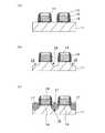
ここで、上述したPMOSFETの製造方法について、図4を用いて説明する。まず、図4(a)に示すように、シリコン基板11の表面側に素子分離領域(図示省略)を形成する。次に、シリコン基板11上にゲート絶縁膜12を介してゲート電極13を形成し、このゲート電極13上にシリコン窒化膜からなるオフセット絶縁膜14を形成する。次いで、ゲート絶縁膜12、ゲート電極13、オフセット絶縁膜14を覆う状態で、シリコン基板11上に、シリコン窒化膜を形成し、ドライエッチング法により、このシリコン窒化膜をエッチバックすることで、ゲート絶縁膜12、ゲート電極13およびオフセット絶縁膜14の両脇にサイドウォール15を形成する。 Here, a method for manufacturing the above-described PMOSFET will be described with reference to FIG. First, as shown in FIG. 4A, an element isolation region (not shown) is formed on the surface side of the
次に、図4(b)に示すように、オフセット絶縁膜14とサイドウォール15をマスクにして、シリコン基板11をエッチングによって掘り下げる、いわゆるリセスエッチングを行うことで、リセス領域16を形成する。その後、希フッ酸を用いた洗浄処理により、シリコン基板11表面の自然酸化膜を除去する。 Next, as shown in FIG. 4B, the
次いで、図4(c)に示すように、リセス領域16、すなわち、掘り下げられたシリコン基板11の表面に、ボロン等のp型不純物を含むシリコンゲルマニウム(SiGe)層17をエピタキシャル成長させる。このSiGe層17が、ソース・ドレイン領域となり、シリコン基板11におけるソース・ドレイン領域に挟まれたゲート電極13直下の領域がチャネル領域18となる。このSiGe層17によるチャネル領域18へのストレス印加により、チャネル領域18が歪むことから、十分なキャリア移動度を有するPMOSFETが形成される。 Next, as shown in FIG. 4C, a silicon germanium (SiGe)
しかし、上述したような半導体装置の製造方法では、図5に示すように、SiGe層17がチャネル領域18となるゲート電極13の直下領域に近いほどSiGe層17によるストレス印加効率は上昇するが、SiGe層17にはボロンからなる不純物が添加されているため、後工程でかかる熱処理、熱工程によりSiGe層17中の不純物が拡散してしまう(拡散領域A)。このため、ショートチャネル効果を引き起こしてしまう、という問題がある。これを防止するためには、ゲート電極13の直下領域とボロンを添加したSiGe層17との距離を広げることが考えられるが、チャネル領域18にかかるストレスが弱まってしまうため、十分なキャリア移動度が得られなくなる。 However, in the method of manufacturing a semiconductor device as described above, as shown in FIG. 5, the stress application efficiency by the
したがって、本発明は、ショートチャネル効果を防止し、十分なキャリア移動度が得られる半導体装置の製造方法および半導体装置を提供することを目的とする。 Therefore, an object of the present invention is to provide a method for manufacturing a semiconductor device and a semiconductor device that can prevent a short channel effect and obtain sufficient carrier mobility.
上述したような目的を達成するために、本発明における半導体装置の製造方法は、次のような工程を順次行うことを特徴としている。まず、シリコン基板上にゲート絶縁膜を介してゲート電極を形成する工程を行う。次に、ゲート電極をマスクにしたエッチングにより、シリコン基板の表面層を掘り下げる工程を行う。次いで、掘り下げられたシリコン基板の表面に、当該シリコン基板側から表面に向かって高濃度となるような濃度勾配を有して不純物が含有されるように、シリコンとシリコンとは格子定数の異なる原子とからなる混晶層をエピタキシャル成長させる工程を行う。そして特に、第3工程で形成する混晶層は、第1の層、第2の層および第3の層からなる3層を順次積層してなり、このような混晶層を形成する第3工程は、次のように行う。先ず、掘り下げられた前記シリコン基板の表面に、前記3層のうちで最も低濃度の不純物が含有されるように、前記第1の層を形成する。次に、第1の層上に、前記第1の層側から表面に向かって、前記第1の層の不純物濃度から前記第3の層の不純物濃度となるような濃度勾配を有して不純物が含有されるように、前記第2の層を形成する。その後、第2の層上に、前記3層のうちで最も高濃度の不純物が含有されるように、前記第3の層を形成する。In order to achieve the above-described object, the semiconductor device manufacturing method according to the present invention is characterized in that the following steps are sequentially performed. First, a step of forming a gate electrode on a silicon substrate via a gate insulating film is performed. Next, a step of digging the surface layer of the silicon substrate is performed by etching using the gate electrode as a mask. Next, silicon and silicon have different lattice constants so that impurities are contained on the surface of the dug silicon substrate with a concentration gradient that increases from the silicon substrate side toward the surface. A step of epitaxially growing a mixed crystal layer comprising: In particular, themixed crystal layer formed in the third step is formed bysequentially stacking three layers including the first layer, the second layer, and the third layer, and a third layer that forms such a mixed crystal layer is formed. The process is performed as follows. First, the first layer is formed so that the lowest concentration of the three layers is contained in the dug-down surface of the silicon substrate. Next, impurities having a concentration gradient on the first layer from the first layer side to the surface so as to be from the impurity concentration of the first layer to the impurity concentration of the third layer. The second layer is formed so that is contained. Thereafter, the third layer is formed on the second layer so as to contain the highest concentration of impurities among the three layers.
このような半導体装置の製造方法によれば、掘り下げられたシリコン基板の表面に、シリコン基板側から表面に向かって高濃度となるような濃度勾配を有して不純物が含有されるように、上記混晶層をエピタキシャル成長させるため、シリコン基板におけるゲート電極直下のチャネル領域近くの混晶層は、表面側と比較して低濃度の不純物が含有された状態となる。これにより、熱処理による混晶層からの不純物の拡散が抑制され、ショートチャネル効果が防止される。また、ゲート電極の直下領域と上記混晶層との距離を広げなくてもよいため、十分なキャリア移動度が得られる。 According to such a method for manufacturing a semiconductor device, the surface of the silicon substrate dug down contains impurities with a concentration gradient that increases from the silicon substrate side toward the surface. In order to epitaxially grow the mixed crystal layer, the mixed crystal layer near the channel region immediately below the gate electrode in the silicon substrate is in a state containing impurities at a lower concentration than the surface side. Thereby, the diffusion of impurities from the mixed crystal layer due to the heat treatment is suppressed, and the short channel effect is prevented. Further, since it is not necessary to increase the distance between the region directly under the gate electrode and the mixed crystal layer, sufficient carrier mobility can be obtained.
また、本発明の半導体装置は、シリコン基板上にゲート絶縁膜を介して設けられたゲート電極と、ゲート電極の両側のシリコン基板が掘り下げられた領域に、シリコンとシリコンとは格子定数の異なる原子とからなる混晶層とを備えた半導体装置において、混晶層には、シリコン基板側から表面に向かって高濃度となるような濃度勾配を有して不純物が含有されていることを特徴としている。そして特に、混晶層は、掘り下げられた前記シリコン基板側から順に第1の層、第2の層および第3の層からなる3層をエピタキシャル成長によって積層してなる。第1の層は、前記3層のうちで最も低濃度の不純物が含有されている。第2の層は、前記第1の層側から表面に向かって、前記第1の層の不純物濃度から前記第3の層の不純物濃度となるような濃度勾配を有して不純物が含有されている。第3の層は、前記3層のうちで最も高濃度の不純物が含有される。In addition, the semiconductor device of the present invention includes a gate electrode provided on a silicon substrate with a gate insulating film interposed therebetween, and atoms having different lattice constants between silicon and silicon in a region where the silicon substrate on both sides of the gate electrode is dug down. In a semiconductor device comprising a mixed crystal layer comprising: a mixed crystal layer, wherein the mixed crystal layer contains impurities with a concentration gradient that increases from the silicon substrate side toward the surface. Yes. In particular, themixed crystal layer is formed by epitaxially growing three layers including a first layer, a second layer, and a third layer in order from the side of the silicon substrate that has been dug down. The first layer contains the lowest concentration of the three layers. The second layer contains impurities with a concentration gradient from the first layer side toward the surface from the impurity concentration of the first layer to the impurity concentration of the third layer. Yes. The third layer contains the highest concentration of impurities among the three layers.
このような半導体装置によれば、混晶層には、シリコン基板側から表面に向かって高濃度となるような濃度勾配を有して不純物が含有されていることから、シリコン基板におけるゲート電極直下のチャネル領域近くの混晶層は、表面側と比較して低濃度の不純物が含有される。これにより、熱処理による混晶層からの不純物の拡散が抑制され、ショートチャネル効果が防止される。また、ゲート電極の直下領域と上記混晶層との距離を広げなくてもよいことから、十分なキャリア移動度が得られる。 According to such a semiconductor device, the mixed crystal layer contains impurities with a concentration gradient that increases from the silicon substrate side to the surface. The mixed crystal layer near the channel region contains a lower concentration of impurities than the surface side. Thereby, the diffusion of impurities from the mixed crystal layer due to the heat treatment is suppressed, and the short channel effect is prevented. Further, since it is not necessary to increase the distance between the region directly under the gate electrode and the mixed crystal layer, sufficient carrier mobility can be obtained.
以上、説明したように、本発明における半導体装置の製造方法および半導体装置によれば、ショートチャネル効果が防止できるとともに、十分なキャリア移動度が得られることから、トランジスタの特性を向上させることができる。 As described above, according to the semiconductor device manufacturing method and the semiconductor device of the present invention, the short channel effect can be prevented and sufficient carrier mobility can be obtained, so that the transistor characteristics can be improved. .
以下、本発明の実施の形態を図面に基づいて詳細に説明する。各実施形態においては、半導体装置の構成を製造工程順に説明する。 Hereinafter, embodiments of the present invention will be described in detail with reference to the drawings. In each embodiment, the configuration of a semiconductor device will be described in the order of manufacturing steps.
(第1実施形態)
本発明の半導体装置の製造方法に係る実施の形態の一例として、PMOSFETの製造方法を例にとり、図1〜図2の製造工程断面図を用いて説明する。なお、背景技術で説明したものと同様の構成には、同一の番号を付して説明する。(First embodiment)
As an example of an embodiment of a method for manufacturing a semiconductor device according to the present invention, a method for manufacturing a PMOSFET will be taken as an example, and a manufacturing process sectional view of FIGS. In addition, the same number is attached | subjected and demonstrated to the structure similar to what was demonstrated by background art.
まず、図1(a)に示すように、単結晶シリコンからなるシリコン基板11を用意し、その表面側に素子分離領域を形成する。この際、例えば、シリコン基板11の表面側に溝を形成し、この溝内に例えば酸化シリコン膜からなる絶縁膜を埋め込んだSTI(shallow trench isolation)構造の素子分離領域を形成する。 First, as shown in FIG. 1A, a
次に、素子分離領域で分離されたシリコン基板11上に、例えばシリコン酸窒化膜からなるゲート絶縁膜12を介して、例えばポリシリコンからなるゲート電極13をパターン形成する。この際、ゲート電極13上に例えばシリコン窒化膜からなるオフセット絶縁膜14が設けられるように、ゲート絶縁膜12、ゲート電極13、およびオフセット絶縁膜14を構成する各材料膜を積層成膜した後に、これらの積層膜をパターンエッチングする。 Next, a
ここで、上記ゲート絶縁膜12の構成材料としては、シリコン酸窒化膜に限定されず、シリコン酸化膜でもよく、ハフニウムやアルミニウムを含む金属酸化膜であってもよい。また、ゲート電極13としては、ポリシリコンに限定されるものではなく、金属材料を含有してもよい。 Here, the constituent material of the
次いで、図1(b)に示すように、ゲート絶縁膜12、ゲート電極13、およびオフセット絶縁膜14を覆う状態で、シリコン基板11上に、例えばシリコン窒化膜15’を成膜する。続いて、図1(c)に示すように、例えばドライエッチング法により、シリコン窒化膜15’(前記図1(b)参照)をエッチバックすることにより、ゲート絶縁膜12、ゲート電極13、およびオフセット絶縁膜14の側壁に、絶縁性のサイドウォール15を形成する。ここでは、このサイドウォール15が、例えばシリコン窒化膜で構成されることとするが、シリコン窒化膜以外でもよく、シリコン酸化膜またはこれらの積層構造で構成されていてもよい。 Next, as shown in FIG. 1B, for example, a
次に、図1(d)に示すように、シリコン基板11の表面を掘り下げるリセスエッチングを行う。この場合には、ゲート電極13上のオフセット絶縁膜14およびサイドウォール15をマスクにしたエッチングにより、シリコン基板11の表面層を掘り下げるリセスエッチングを行うことで、80nm程度の深さのリセス領域16を形成する。このリセスエッチングにおいては、等方性のエッチングを行うことにより、サイドウォール15の下方にまでリセス領域16が広げられるようにする。その後、希フッ酸を用いた洗浄処理により、シリコン基板11表面の自然酸化膜を除去する。なお、ここでは、サイドウォール15が設けられた状態で、リセスエッチングを行う例について説明するが、サイドウォール15を設けずに、リセスエッチングを行う場合であっても、本発明は適用可能である。 Next, as shown in FIG. 1D, recess etching for digging the surface of the
次いで、リセス領域16の表面、すなわち掘り下げられたシリコン基板11の表面に、シリコンとシリコンとは格子定数の異なる原子との混晶層を、不純物を含む状態で、エピタキシャル成長させる。ここでは、PMOSFETを形成することから、例えばボロンからなる不純物を含むシリコン(Si)とシリコンよりも格子定数の大きい原子(Ge)とからなるSiGe層(混晶層)をエピタキシャル成長させる。 Next, a mixed crystal layer of silicon and atoms having different lattice constants is epitaxially grown on the surface of the
この際、本発明の特徴的な構成として、掘り下げられたシリコン基板11の表面に、シリコン基板11側から表面に向かって高濃度となるような濃度勾配を有してボロンが含有されるように、上記SiGe層をエピタキシャル成長させる。ここでは、上記SiGe層が、第1のSiGe層(第1の層)、第2のSiGe層(第2の層)および第3のSiGe層(第3の層)からなる3層を順次積層して構成されることとする。 At this time, as a characteristic configuration of the present invention, boron is contained on the surface of the
具体的には、図2(e)に示すように、掘り下げられたシリコン基板11の表面、すなわち、リセス領域16の表面に、上記3層のうち最も低濃度のボロンが含有されるように、第1のSiGe層21aを形成する。ここでは、ボロン濃度が1×1018cm3〜1×1019cm3となるように、1nm〜30nmの膜厚で第1のSiGe層21aをエピタキシャル成長させる。Specifically, as shown in FIG. 2 (e), the surface of the
上記第1のSiGe層21aの成膜条件としては、成膜ガスとして、ジクロロシラン(Dichlorosilane(DCS))、水素(H2)により1.5vol%に希釈された水素化ゲルマニウム(GeH4)、塩化水素(HCl)および水素(H2)により100ppmに希釈されたジボラン(B2H6)を用い、ガス流量をDCS/GeH4/HCl/B2H6=10〜100/10〜100/10〜100/1〜50(ml/min)とし、処理温度を650℃〜750℃、処理圧力を1.3kPa〜13.3kPaに設定する。ただし、上記ガス流量は、標準状態における体積流量を示すものとし、これ以降に示すガス流量についても同様であることとする。As the film forming conditions for the
ここで、この低濃度の不純物が含有される第1のSiGe層21aは、後述するように、形成するSiGe層の中でもチャネル領域近くに配置されるため、熱処理によるSiGe層からのボロンの拡散が抑制され、ショートチャネル効果が防止される。そして、ショートチャネル効果を確実に防止するため、形成するPMOSFETのキャリア移動度を低下させない範囲で、上記第1のSiGe層21aは、上記膜厚の範囲内でも10nm〜30nm程度の膜厚を有して形成されることが、さらに好ましい。 Here, since the
なお、背景技術で説明したように、リセス領域の表面に、成膜条件を変えずにSiGe層を直接形成する場合でも、成膜の都合上、リセス領域の表面に低濃度の不純物が含有されるSiGe層が形成される場合もあるが、本実施形態の第1のSiGe層21aはそれとは異なり、成膜条件を変えて、所定の膜厚となるように、低濃度の不純物が含有される第1のSiGe層21aを形成する。 As described in the background art, even when the SiGe layer is directly formed on the surface of the recess region without changing the film formation conditions, a low concentration impurity is contained on the surface of the recess region for the convenience of film formation. However, unlike the
次に、図2(f)に示すように、第1のSiGe層21a上に、第1のSiGe層21a側から表面に向かって、第1のSiGe層21aの不純物濃度から後述する第3のSiGe層の不純物濃度まで連続的に変化するような濃度勾配を有して不純物が含有されるように、第2のSiGe層21bをエピタキシャル成長させる。ここでは、第1のSiGe層21aのボロンの濃度範囲が1×1018cm3〜1×1019cm3であり、後述するように、第3のSiGe層のボロンの濃度範囲が1×1019cm3〜5×1020cm3であることから、第1のSiGe層21a側から表面に向かって、1×1018cm3〜1×1019cm3の濃度範囲から1×1019cm3〜5×1020cm3の濃度範囲まで連続的に高濃度となるような濃度勾配を有してボロンが含有されるように、第2のSiGe層21bを形成する。この第2のSiGe層21bの膜厚は、1nm〜20nmであることとする。Next, as shown in FIG. 2 (f), on the
この第2のSiGe層21bの成膜条件としては、上記第1のSiGe層21aと同一の成膜ガスを用い、成膜ガスのうち、DCS、GeH4、HClについては、ガス流量をDCS/GeH4/HCl=10〜100/10〜100/10〜100(ml/min)とする。そして、H2により100ppmに希釈されたB2H6のガス流量を1〜50(ml/min)から50〜300(ml/min)に連続的に変化させる。また、処理温度を650℃〜750℃、処理圧力を1.3kPa〜13.3kPaに設定する。As the film forming conditions for the
ここで、3層のうちで最も不純物濃度の低い第1のSiGe層21aと、後述する最も不純物濃度の高い第3のSiGe層との間に、上記第2のSiGe層21bが介在することで、第1のSiGe層21aと第3のSiGe層との不純物の濃度差による成膜の不具合が緩和される。このため、第1のSiGe層21aと第3のSiGe層の不純物の濃度差が小さい場合には、第2のSiGe層21bを形成しなくてもよい。また、ここでは、第1のSiGe層21a側から第3のSiGe層側に向かって、連続的に高濃度となるような濃度勾配を有して不純物が含有されるように、第2のSiGe層21bを形成することとしたが、濃度勾配は段階的であってもよい。この場合には、B2H6のガス流量を段階的に変化させる。Here, the
次に、図2(g)に示すように、第2のSiGe層21b上に、上記3層のうちで最も高濃度の不純物が含有されるように、第3のSiGe層21cを形成する。ここでは、ボロン濃度が1×1019cm3〜5×1020cm3となるように、50nm〜100nmの膜厚で第3のSiGe層21cをエピタキシャル成長させる。Next, as shown in FIG. 2G, the
この第3のSiGe層21cの成膜条件としては、上記第1のSiGe層21a、第2のSiGe層21bと同一の成膜ガスを用い、ガス流量をDCS/GeH4/HCl/B2H6=10〜100/10〜100/10〜100/50〜300(ml/min)とし、処理温度を650℃〜750℃、処理圧力を1.3kPa〜13.3kPaに設定する。As the film forming conditions for the
これにより、リセス領域16の表面に、第1のSiGe層21a、第2のSiGe層21bおよび第3のSiGe層21cを順次積層してなるSiGe層21が形成される。ここで、上記リセス領域16は80nm程度の深さで形成されることから、第1のSiGe層21a、第2のSiGe層21bおよび第3のSiGe層21cで順次埋め込まれ、第3のSiGe層21cは、シリコン基板11の表面から盛り上がった状態となる。そして、このSiGe層21には、シリコン基板11側から表面に向かって高濃度となるような濃度勾配を有してボロンからなる不純物が含有されている。 As a result, the
このSiGe層21が、本実施形態の製造方法により形成されるPMOSFETのソース・ドレイン領域となり、SiGe層21により挟まれたゲート電極13直下のシリコン基板11の領域がチャネル領域18となる。 The
この後の工程は、通常のPMOSFETの製造方法と同様に行う。例えばSiGe層21の表面側をシリサイド化して、シリサイド層を形成してもよい。この際、上述したように、チャネル領域18近くに配置される第1のSiGe層21aには、低濃度の不純物が含有されていることから、SiGe層21を形成した後に熱処理を行う場合でも不純物の拡散Aが抑制され、ショートチャネル効果が防止される。 The subsequent steps are performed in the same manner as in a normal PMOSFET manufacturing method. For example, the surface side of the
以上のようにして、SiGe層21によるチャネル領域18へのストレス印加(圧縮応力)により、チャネル領域18を歪ませたPMOSFETが製造される。 As described above, a PMOSFET in which the
このような半導体装置の製造方法およびこれにより得られる半導体装置によれば、シリコン基板11側から表面に向かって高濃度となるような濃度勾配を有して不純物が含有されるように、SiGe層21をエピタキシャル成長させることから、熱処理によるSiGe層21からの不純物の拡散Aが抑制され、ショートチャネル効果が防止される。特に、本実施形態によれば、SiGe層21を3層で構成し、チャネル領域18に近い第1のSiGe層21aを他の層と比較して低濃度の不純物が含有されるように形成するため、ショートチャネル効果を確実に防止することができる。また、上記SiGe層21とゲート電極13の直下領域からの距離を広げなくてもよいため、十分なキャリア移動度が得られる。したがって、トランジスタの特性を向上させることができる。 According to such a method of manufacturing a semiconductor device and the semiconductor device obtained thereby, the SiGe layer is formed so as to contain impurities with a concentration gradient that increases from the
さらに、本実施形態の半導体装置の製造方法によれば、成膜ガスを変えずに、成膜条件を変更するだけの一連の作業で、不純物の濃度勾配を有するSiGe層21を成膜することができるため、生産性にも優れている。 Furthermore, according to the method for manufacturing a semiconductor device of the present embodiment, the
なお、上記第1実施形態においては、PMOSFETのソース・ドレイン領域となるSiGe層に、不純物としてボロンを含有させる例について説明したが、不純物としては、上記ボロン以外に、ガリウム(Ga)またはインジウム(In)を用いてもよい。不純物として、例えばGaを用いる場合には、上述した第1実施形態において、成膜ガスとして用いたB2H6の代わりに、トリエチルガリウム(Ga(C2H5)3)またはトリメチルガリウム(Ga(CH3)3)を適用する。また、不純物として、例えばInを用いる場合には、成膜ガスとして用いたB2H6の代わりに、トリエチルインジウム(In(C2H5)3)またはトリメチルインジウム(In(CH3)3)を適用する。In the first embodiment, an example has been described in which boron is contained as an impurity in the SiGe layer serving as the source / drain region of the PMOSFET. However, as the impurity, in addition to boron, gallium (Ga) or indium ( In) may also be used. For example, when Ga is used as the impurity, triethylgallium (Ga (C2 H5 )3 ) or trimethylgallium (Ga) is used instead of B2 H6 used as the film forming gas in the first embodiment described above. (CH3 )3 ) applies. For example, when In is used as an impurity, triethylindium (In (C2 H5 )3 ) or trimethylindium (In (CH3 )3 ) is used instead of B2 H6 used as a film forming gas. Apply.
(第2実施形態)
上記第1実施形態では、PMOSFETの製造方法を例にとり説明したが、本実施形態においてはNMOSFETの製造方法を例にとり、図3を用いて説明する。なお、シリコン基板11の表面を掘り下げるまでの工程は、図1(a)〜(d)を用いて説明した工程と同様に行うこととする。(Second Embodiment)
In the first embodiment, the method for manufacturing the PMOSFET has been described as an example. However, in the present embodiment, the method for manufacturing the NMOSFET will be described as an example with reference to FIG. It should be noted that the process until the surface of the
NMOSFETを製造する場合には、まず、図3(a)に示すように、リセス領域16の表面、すなわち、掘り下げられたシリコン基板11の表面に、例えば砒素(As)からなる不純物を含むシリコン(Si)とシリコンよりも格子定数の小さい原子(C)とからなるシリコン炭素(SiC)層(混晶層)をエピタキシャル成長させる。 When manufacturing an NMOSFET, first, as shown in FIG. 3A, the surface of the
この場合であっても、掘り下げられたシリコン基板11の表面に、シリコン基板11側から表面に向かって高濃度となるような濃度勾配を有してAsが含有されるように、SiC層をエピタキシャル成長させる。ここでは、第1実施形態と同様に、上記SiC層が、第1のSiC層(第1の層)、第2のSiC層(第2の層)および第3のSiC層(第3の層)からなる3層を順次積層して構成されることとする。 Even in this case, the SiC layer is epitaxially grown so that As is contained on the surface of the dug down
具体的には、掘り下げられたシリコン基板11の表面に、上記3層のうち最も低濃度の不純物が含有されるように、第1のSiC層22aを形成する。ここでは、As濃度が1×1018cm3〜1×1019cm3となるように、1nm〜30nmの膜厚で第1のSiC層22aを形成することとする。Specifically, the
この第1のSiC層22aの成膜条件としては、成膜ガスとして、DCS、水素(H2)により1vol%に希釈されたモノメチルシラン(SiH3CH3)、HCl、水素(H2)により1vol%に希釈された水素化砒素(AsH3)を用い、ガス流量をDCS/SiH3CH3/HCl/AsH3=10〜100/1〜50/10〜100/1〜25(ml/min)とし、処理温度を650℃〜750℃、処理圧力を1.3kPa〜13.3kPaに設定する。As the film formation conditions for the
ここで、この低濃度の不純物が含有される第1のSiC層22aは、後述するように、形成するSiC層の中でもチャネル領域に近くに配置されるため、熱処理によるSiC層からのAsの拡散が抑制され、ショートチャネル効果が防止される。そして、ショートチャネル効果を確実に防止するため、形成するNMOSFETのキャリア移動度を低下させない範囲で、上記第1のSiC層22aは、上記膜厚の範囲内でも10nm〜30nm程度の膜厚を有して形成されることが、さらに好ましい。 Here, since the
次に、図3(b)に示すように、第1のSiC層22a上に、第1のSiC層22a側から表面に向かって、第1のSiC層22aの不純物濃度から後述する第3のSiC層の不純物濃度まで連続的に変化するような濃度勾配を有して不純物が含有されるように、第2のSiC層22bを形成する。ここでは、第1のSiC層22aのAsの濃度範囲が1×1018cm3〜1×1019cm3であり、後述するように、第3のSiC層のAsの濃度範囲が1×1019cm3〜5×1020cm3であることから、第1のSiC層22a側から表面に向かって、1×1018cm3〜1×1019cm3の濃度範囲から1×1019cm3〜5×1020cm3の濃度範囲まで連続的に高濃度となるような濃度勾配を有してAsが含有されるように、第2のSiC層22bを形成する。この第2のSiC層22bの膜厚は、1nm〜20nmであることとする。Next, as shown in FIG. 3B, a
この第2のSiC層22bの成膜条件としては、上記第1のSiC層22aと同一の成膜ガスを用い、DCS、SiH3CH3、HClについては、第1のSiC層22aと同様に、ガス流量をDCS/SiH3CH3/HCl=10〜100/1〜50/10〜100/1〜25(ml/min)に設定する。そして、H2により1vol%に希釈されたAsH3のガス流量を1〜25(ml/min)から25〜50(ml/min)となるように、連続的に変化させる。また、処理温度を650℃〜750℃、処理圧力を1.3kPa〜13.3kPaに設定する。As the film formation conditions for the
ここで、3層のうちで最も不純物濃度の低い第1のSiC層22aと、後述する最も不純物濃度の高い第3のSiC層との間に、上記第2のSiC層22bが介在されることで、第1のSiC層22aと第3のSiC層との不純物の濃度差による成膜の不具合が緩和される。このため、第1のSiC層22aと第3のSiC層の不純物の濃度差が小さい場合には、第2のSiC層22bを形成しなくてもよい。また、ここでは、第1のSiC層22a側から第3のSiC層22c側に向かって、連続的に高濃度となるような濃度勾配を有して不純物が含有されるように、第2のSiC層22bを形成することとしたが、濃度勾配は段階的であってもよい。この場合には、AsH3のガス流量を段階的に変化させる。Here, the
次に、図3(c)に示すように、第2のSiC層22b上に、上記3層のうちで最も高濃度の不純物が含有されるように、第3のSiC層22cを形成する。ここでは、As濃度が1×1019cm3〜5×1020cm3となるように、50nm〜100nmの膜厚で第3のSiC層22cを形成する。Next, as shown in FIG. 3C, a
この第3のSiC層22cの成膜条件としては、上記第1のSiC層22a、第2のSiC層22bと同一の成膜ガスを用い、ガス流量をDCS/SiH3CH3/HCl/AsH3=10〜100/1〜50/10〜100/25〜50(ml/min)に設定する。また、処理温度を650℃〜750℃、処理圧力を1.3kPa〜13.3kPaに設定する。As the film formation conditions for the
これにより、リセス領域16の表面に、第1のSiC層22a、第2のSiC層22bおよび第3のSiC層22cを順次積層してなるSiC層22が形成される。ここで、上記リセス領域16は80nm程度の深さで形成されることから、第1のSiC層22a、第2のSiC層22bおよび第3のSiC層22cで順次埋め込まれ、第3のSiC層22cは、シリコン基板11の表面から盛り上がった状態となる。そして、このSiC層22には、シリコン基板11側から表面に向かって高濃度となるような濃度勾配を有してAsからなる不純物が含有されている。 Thereby, a
このSiC層22が、本実施形態の製造方法により形成されるNMOSFETのソース・ドレイン領域となり、SiC層22により挟まれたゲート電極13直下のシリコン基板11の領域がチャネル領域18となる。 This
この後の工程は、通常のNMOSFETの製造方法と同様に行う。例えばSiC層22の表面側をシリサイド化して、シリサイド層を形成してもよい。この際、上述したように、チャネル領域18近くに配置される第1のSiC層22aには、低濃度の不純物が含有されていることから、SiC層22を形成した後に熱処理を行う場合でも不純物の拡散Aが抑制され、ショートチャネル効果が防止される。 The subsequent steps are performed in the same manner as in a normal NMOSFET manufacturing method. For example, the silicide layer may be formed by siliciding the surface side of the
以上のようにして、SiC層22によるチャネル領域18へのストレス印加(引っ張り応力)により、チャネル領域18を歪ませたNMOSFETが製造される。 As described above, an NMOSFET in which the
このような半導体装置の製造方法およびこれにより得られる半導体装置によっても、シリコン基板11側ら表面に向かって高濃度となるような濃度勾配を有して不純物が含有されるように、SiC層22をエピタキシャル成長させることから、熱処理によるSiC層22からの不純物の拡散が抑制され、ショートチャネル効果が防止される。特に、本実施形態によれば、SiC層22を3層で構成し、チャネル領域18に近い第1のSiC層22aを他の層と比較して低濃度の不純物が含有されるように形成することで、ショートチャネル効果を確実に防止することができる。また、上記SiC層22とゲート電極13の直下領域からの距離を広げなくてもよいため、十分なキャリア移動度が得られる。したがって、トランジスタの特性を向上させることができる。 Also in such a method for manufacturing a semiconductor device and the semiconductor device obtained thereby, the
(変形例1)
なお、上記第2実施形態においては、NMOSFETのソース・ドレイン領域となるSiC層に、不純物としてAsを含有させる例について説明したが、不純物としては、上記As以外に、リン(P)を用いてもよい。(Modification 1)
In the second embodiment, the example in which As is included in the SiC layer serving as the source / drain region of the NMOSFET has been described. However, as the impurity, phosphorus (P) is used in addition to As. Also good.
この場合にも、1×1018cm3〜1×1019cm3の濃度範囲でPからなる不純物が含有されるように、1nm〜30nmの膜厚で第1のSiC層22aを形成する。Also in this case, the
この第1のSiC層22aの成膜条件としては、成膜ガスとして、DCS、H2により1vol%に希釈されたSiH3CH3、HCl、H2により50ppmに希釈された水素化リン(PH3)を用い、ガス流量をDCS/SiH3CH3/HCl/PH3=10〜100/1〜50/10〜100/1〜150(ml/min)とし、処理温度を650℃〜750℃、処理圧力を1.3kPa〜13.3kPaに設定する。The film formation conditions for the
次に、第1のSiC層22a上に、第1のSiC層22a側から表面に向かって、1×1018cm3〜1×1019cm3の濃度範囲から1×1019cm3〜5×1020cm3の濃度範囲まで高濃度となるような濃度勾配を有してPからなる不純物が含有されるように、第2のSiC層22bを1nm〜20nmの膜厚で形成する。Next, on the
この第2のSiC層22bの成膜条件としては、上記第1のSiC層22aと同一の成膜ガスを用い、DCS、SiH3CH3、HClについては、ガス流量をDCS/SiH3CH3/HCl=10〜100/1〜50/10〜100に設定する。そして、H2により50ppmに希釈されたPH3のガス流量を1〜150(ml/min)から150〜300(ml/min)となるように、連続的にまたは段階的に変化させる。また、処理温度を650℃〜750℃、処理圧力を1.3kPa〜13.3kPaに設定する。As the film formation conditions for the
次いで、第2のSiC層22b上に、1×1019cm3〜5×1020cm3の濃度範囲でPからなる不純物が含有されるように、50nm〜100nmの膜厚で第3のSiC層22cを形成する。Next, a third SiC film having a thickness of 50 nm to 100 nm is contained on the
この第3のSiC層22cの成膜条件としては、上記第1のSiC層22a、第2のSiC層22cと同一の成膜ガスを用い、ガス流量をDCS/SiH3CH3/HCl/PH3=10〜100/1〜50/10〜100/150〜300(ml/min)に設定する。また、処理温度を650℃〜750℃、処理圧力を1.3kPa〜13.3kPaに設定する。As the film formation conditions for the
このようなNMOSFETの製造方法およびNMOSFETによっても、上述した第2実施形態と同様の効果を奏することができる。 The same effects as those of the second embodiment described above can also be achieved by such an NMOSFET manufacturing method and NMOSFET.
なお、上述した第1実施形態および第2実施形態ならびに変形例1においては、SiGe層またはSiC層からなる混晶層を、第1の層、第2の層および第3の層が順次積層された3層で構成し、不純物が所定の濃度範囲で維持されるように第1の層および第3の層を形成するとともに、第1の層側から第3の層側に向かって連続的に高濃度となるような濃度勾配を有して第2の層を形成する例について説明した。しかし、本発明はこれに限定されず、シリコン基板側から表面に向かって段階的に高濃度となるような濃度勾配を有して不純物が含有される複数層で混晶層を形成してもよく、連続的に高濃度となるような濃度勾配を有して不純物が含有される単一層で混晶層を形成してもよい。ただし、混晶層のうちチャネル領域に近い部分は、不純物が低濃度で維持された領域を、10nm〜30nmの膜厚で有することが好ましい。 In the first embodiment, the second embodiment, and the modification example 1 described above, the first layer, the second layer, and the third layer are sequentially stacked in the mixed crystal layer including the SiGe layer or the SiC layer. The first layer and the third layer are formed so that impurities are maintained in a predetermined concentration range, and continuously from the first layer side to the third layer side. The example in which the second layer is formed with a concentration gradient that results in a high concentration has been described. However, the present invention is not limited to this, and the mixed crystal layer may be formed of a plurality of layers containing impurities with a concentration gradient that gradually increases from the silicon substrate side toward the surface. Alternatively, the mixed crystal layer may be formed as a single layer containing impurities with a concentration gradient that continuously increases. However, the portion close to the channel region in the mixed crystal layer preferably has a region in which impurities are maintained at a low concentration with a thickness of 10 nm to 30 nm.
また、上述した実施形態においては、PMOSFETとNMOSFETとをそれぞれ形成する半導体装置の製造方法の例について説明したが、PMOSFETとNMOSFETの両方を搭載したCMOS(Complementary Metal Oxide Semiconductor)FETを形成する場合にも本発明は適用可能である。 In the above-described embodiment, an example of a method of manufacturing a semiconductor device in which a PMOSFET and an NMOSFET are respectively formed has been described. However, in the case of forming a CMOS (Complementary Metal Oxide Semiconductor) FET in which both a PMOSFET and an NMOSFET are mounted. The present invention is also applicable.
11…シリコン基板、12…ゲート絶縁膜、13…ゲート電極、21…SiGe層、21a…第1のSiGe層、21b…第2のSiGe層、21c…第3のSiGe層、22…SiGe層、22a…第1のSiC層、22b…第2のSiC層、22c…第3のSiC層 DESCRIPTION OF
Claims (3)
Translated fromJapanese前記ゲート電極をマスクにしたエッチングにより、前記シリコン基板の表面層を掘り下げる第2工程と、
掘り下げられた前記シリコン基板の表面に、当該シリコン基板側から表面に向かって高濃度となるような濃度勾配を有して不純物が含有されるように、シリコンとシリコンとは格子定数の異なる原子とからなる混晶層をエピタキシャル成長させる第3工程とを有する半導体装置の製造方法において、
前記混晶層が、第1の層、第2の層および第3の層からなる3層を順次積層してなり、
前記第3工程では、
掘り下げられた前記シリコン基板の表面に、前記3層のうちで最も低濃度の不純物が含有されるように、前記第1の層を形成する工程と、
前記第1の層上に、前記第1の層側から表面に向かって、前記第1の層の不純物濃度から前記第3の層の不純物濃度となるような濃度勾配を有して不純物が含有されるように、前記第2の層を形成する工程と、
前記第2の層上に、前記3層のうちで最も高濃度の不純物が含有されるように、前記第3の層を形成する工程とを行う
ことを特徴とする半導体装置の製造方法。A first step of forming a gate electrode on a silicon substrate via a gate insulating film;
A second step of digging a surface layer of the silicon substrate by etching using the gate electrode as a mask;
Silicon and silicon have different lattice constants so that impurities are contained on the surface of the silicon substrate that has been dug down so as to have a concentration gradient from the silicon substrate side toward the surface. And a third step of epitaxially growing a mixed crystal layer comprising:
The mixed crystal layer is formed by sequentially stacking three layers including a first layer, a second layer, and a third layer,
In the third step,
Forming the first layer so that the lowest concentration of the three layers is contained in the dug down surface of the silicon substrate;
Impurities are contained on the first layer from the first layer side to the surface with a concentration gradient from the impurity concentration of the first layer to the impurity concentration of the third layer from the first layer side to the surface. Forming the second layer, and
Forming the third layer on the second layer so as to contain the highest concentration of the impurities among the three layers. A method of manufacturing a semiconductor device, comprising:
前記半導体装置がp型の電界効果トランジスタであり、
前記第3工程では、前記シリコン基板の表面に、前記濃度勾配を有してp型の不純物が含有されるように、シリコンとゲルマニウムとからなる前記混晶層をエピタキシャル成長させる
ことを特徴とする半導体装置の製造方法。In the manufacturing method of the semiconductor device according to claim 1,
The semiconductor device is a p-type field effect transistor;
In the third step, the mixed crystal layer made of silicon and germanium is epitaxially grown on the surface of the silicon substrate so as to contain a p-type impurity having the concentration gradient. Device manufacturing method.
前記半導体装置がn型の電界効果トランジスタであり、
前記第3工程では、前記シリコン基板の表面に、前記濃度勾配を有してn型の不純物が含有されるように、シリコンと炭素とからなる前記混晶層をエピタキシャル成長させる
ことを特徴とする半導体装置の製造方法。In the manufacturing method of the semiconductor device according to claim 1,
The semiconductor device is an n-type field effect transistor;
In the third step, the mixed crystal layer composed of silicon and carbon is epitaxially grown on the surface of the silicon substrate so as to contain the n-type impurity having the concentration gradient. Device manufacturing method.
Priority Applications (6)
| Application Number | Priority Date | Filing Date | Title |
|---|---|---|---|
| JP2006121605AJP4345774B2 (en) | 2006-04-26 | 2006-04-26 | Manufacturing method of semiconductor device |
| TW096112761ATWI344212B (en) | 2006-04-26 | 2007-04-11 | Method of manufacturing semiconductor device, and semiconductor device |
| US11/739,792US7510925B2 (en) | 2006-04-26 | 2007-04-25 | Method of manufacturing semiconductor device, and semiconductor device |
| KR1020070040877AKR101358949B1 (en) | 2006-04-26 | 2007-04-26 | Method of manufacturing semiconductor device, and semiconductor device |
| CNA2007101010655ACN101064257A (en) | 2006-04-26 | 2007-04-26 | Method of manufacturing semiconductor device, and semiconductor device |
| US16/184,766USRE49803E1 (en) | 2006-04-26 | 2018-11-08 | Method of manufacturing semiconductor device, and semiconductor device |
Applications Claiming Priority (1)
| Application Number | Priority Date | Filing Date | Title |
|---|---|---|---|
| JP2006121605AJP4345774B2 (en) | 2006-04-26 | 2006-04-26 | Manufacturing method of semiconductor device |
Publications (2)
| Publication Number | Publication Date |
|---|---|
| JP2007294707A JP2007294707A (en) | 2007-11-08 |
| JP4345774B2true JP4345774B2 (en) | 2009-10-14 |
Family
ID=38648812
Family Applications (1)
| Application Number | Title | Priority Date | Filing Date |
|---|---|---|---|
| JP2006121605AActiveJP4345774B2 (en) | 2006-04-26 | 2006-04-26 | Manufacturing method of semiconductor device |
Country Status (5)
| Country | Link |
|---|---|
| US (2) | US7510925B2 (en) |
| JP (1) | JP4345774B2 (en) |
| KR (1) | KR101358949B1 (en) |
| CN (1) | CN101064257A (en) |
| TW (1) | TWI344212B (en) |
Families Citing this family (340)
| Publication number | Priority date | Publication date | Assignee | Title |
|---|---|---|---|---|
| US8017487B2 (en)* | 2006-04-05 | 2011-09-13 | Globalfoundries Singapore Pte. Ltd. | Method to control source/drain stressor profiles for stress engineering |
| US7687337B2 (en)* | 2007-07-18 | 2010-03-30 | Freescale Semiconductor, Inc. | Transistor with differently doped strained current electrode region |
| WO2009093328A1 (en)* | 2008-01-25 | 2009-07-30 | Fujitsu Microelectronics Limited | Semiconductor device and method for production thereof |
| WO2009122542A1 (en)* | 2008-03-31 | 2009-10-08 | 富士通マイクロエレクトロニクス株式会社 | Semiconductor device and method for manufacturing the same |
| US7902009B2 (en)* | 2008-12-11 | 2011-03-08 | Intel Corporation | Graded high germanium compound films for strained semiconductor devices |
| DE102009006884B4 (en)* | 2009-01-30 | 2011-06-30 | Advanced Micro Devices, Inc., Calif. | A method of fabricating a transistor device having in situ generated drain and source regions with a strain-inducing alloy and a gradually varying dopant profile and corresponding transistor device |
| US9394608B2 (en) | 2009-04-06 | 2016-07-19 | Asm America, Inc. | Semiconductor processing reactor and components thereof |
| JP5381382B2 (en) | 2009-06-19 | 2014-01-08 | 富士通セミコンダクター株式会社 | Semiconductor device and manufacturing method thereof |
| US8802201B2 (en) | 2009-08-14 | 2014-08-12 | Asm America, Inc. | Systems and methods for thin-film deposition of metal oxides using excited nitrogen-oxygen species |
| JP5287621B2 (en)* | 2009-09-10 | 2013-09-11 | 富士通セミコンダクター株式会社 | Semiconductor device |
| US8236660B2 (en)* | 2010-04-21 | 2012-08-07 | International Business Machines Corporation | Monolayer dopant embedded stressor for advanced CMOS |
| US8299535B2 (en)* | 2010-06-25 | 2012-10-30 | International Business Machines Corporation | Delta monolayer dopants epitaxy for embedded source/drain silicide |
| KR101703096B1 (en) | 2010-09-02 | 2017-02-07 | 삼성전자 주식회사 | Method of fabricating semiconductor device |
| US8901537B2 (en) | 2010-12-21 | 2014-12-02 | Intel Corporation | Transistors with high concentration of boron doped germanium |
| US9484432B2 (en) | 2010-12-21 | 2016-11-01 | Intel Corporation | Contact resistance reduction employing germanium overlayer pre-contact metalization |
| US8455930B2 (en)* | 2011-01-05 | 2013-06-04 | Taiwan Semiconductor Manufacturing Company, Ltd. | Strained semiconductor device with facets |
| CN102709183B (en)* | 2011-03-28 | 2016-08-03 | 中芯国际集成电路制造(上海)有限公司 | The method being used for producing the semiconductor devices |
| US8338279B2 (en) | 2011-03-30 | 2012-12-25 | International Business Machines Corporation | Reduced pattern loading for doped epitaxial process and semiconductor structure |
| US20130023129A1 (en) | 2011-07-20 | 2013-01-24 | Asm America, Inc. | Pressure transmitter for a semiconductor processing environment |
| JP5875143B2 (en)* | 2011-08-26 | 2016-03-02 | 学校法人関西学院 | Manufacturing method of semiconductor wafer |
| CN103000499B (en)* | 2011-09-14 | 2015-12-16 | 中芯国际集成电路制造(上海)有限公司 | A kind of germanium silicon boron outer layer growth method |
| US8927374B2 (en)* | 2011-10-04 | 2015-01-06 | Taiwan Semiconductor Manufacturing Company, Ltd. | Semiconductor device and fabrication method thereof |
| US9017481B1 (en) | 2011-10-28 | 2015-04-28 | Asm America, Inc. | Process feed management for semiconductor substrate processing |
| CN103107070B (en)* | 2011-11-14 | 2017-11-07 | 联华电子股份有限公司 | Semiconductor device and method for manufacturing epitaxial layer |
| CN103187299B (en)* | 2011-12-31 | 2015-08-05 | 中芯国际集成电路制造(上海)有限公司 | The formation method of transistor |
| US8889523B2 (en)* | 2012-01-02 | 2014-11-18 | United Microelectronics Corp. | Semiconductor process |
| US9190471B2 (en) | 2012-04-13 | 2015-11-17 | Globalfoundries U.S.2 Llc | Semiconductor structure having a source and a drain with reverse facets |
| CN103681496B (en)* | 2012-09-04 | 2016-04-27 | 中芯国际集成电路制造(上海)有限公司 | A kind of manufacture method of semiconductor device |
| US10714315B2 (en) | 2012-10-12 | 2020-07-14 | Asm Ip Holdings B.V. | Semiconductor reaction chamber showerhead |
| CN103794503A (en)* | 2012-10-30 | 2014-05-14 | 中芯国际集成电路制造(上海)有限公司 | Manufacturing method of MOS transistor |
| US20160376700A1 (en) | 2013-02-01 | 2016-12-29 | Asm Ip Holding B.V. | System for treatment of deposition reactor |
| US10134896B2 (en)* | 2013-03-01 | 2018-11-20 | Taiwan Semiconductor Manufacturing Co., Ltd. | Cyclic deposition etch chemical vapor deposition epitaxy to reduce EPI abnormality |
| US8940595B2 (en)* | 2013-03-15 | 2015-01-27 | International Business Machines Corporation | Faceted intrinsic epitaxial buffer layer for reducing short channel effects while maximizing channel stress levels |
| CN104701149A (en)* | 2013-12-04 | 2015-06-10 | 中芯国际集成电路制造(上海)有限公司 | Semiconductor device and forming method thereof |
| US9543387B2 (en)* | 2014-03-10 | 2017-01-10 | Taiwan Semiconductor Manufacturing Company Ltd. | Semiconductor device and manufacturing method thereof |
| US11015245B2 (en) | 2014-03-19 | 2021-05-25 | Asm Ip Holding B.V. | Gas-phase reactor and system having exhaust plenum and components thereof |
| CN105304481A (en)* | 2014-06-10 | 2016-02-03 | 联华电子股份有限公司 | Semiconductor element and manufacturing method thereof |
| US10084063B2 (en)* | 2014-06-23 | 2018-09-25 | Taiwan Semiconductor Manufacturing Company Ltd. | Semiconductor device and manufacturing method thereof |
| US10858737B2 (en) | 2014-07-28 | 2020-12-08 | Asm Ip Holding B.V. | Showerhead assembly and components thereof |
| US9890456B2 (en) | 2014-08-21 | 2018-02-13 | Asm Ip Holding B.V. | Method and system for in situ formation of gas-phase compounds |
| US10941490B2 (en) | 2014-10-07 | 2021-03-09 | Asm Ip Holding B.V. | Multiple temperature range susceptor, assembly, reactor and system including the susceptor, and methods of using the same |
| US9991343B2 (en)* | 2015-02-26 | 2018-06-05 | Taiwan Semiconductor Manufacturing Company Ltd. | LDD-free semiconductor structure and manufacturing method of the same |
| US10276355B2 (en) | 2015-03-12 | 2019-04-30 | Asm Ip Holding B.V. | Multi-zone reactor, system including the reactor, and method of using the same |
| US20180151733A1 (en)* | 2015-06-19 | 2018-05-31 | Intel Corporation | Carbon-based interface for epitaxially grown source/drain transistor regions |
| US10458018B2 (en) | 2015-06-26 | 2019-10-29 | Asm Ip Holding B.V. | Structures including metal carbide material, devices including the structures, and methods of forming same |
| US9691901B2 (en)* | 2015-10-02 | 2017-06-27 | United Microelectronics Corp. | Semiconductor device |
| US10211308B2 (en) | 2015-10-21 | 2019-02-19 | Asm Ip Holding B.V. | NbMC layers |
| US11139308B2 (en) | 2015-12-29 | 2021-10-05 | Asm Ip Holding B.V. | Atomic layer deposition of III-V compounds to form V-NAND devices |
| US10529554B2 (en) | 2016-02-19 | 2020-01-07 | Asm Ip Holding B.V. | Method for forming silicon nitride film selectively on sidewalls or flat surfaces of trenches |
| US10343920B2 (en) | 2016-03-18 | 2019-07-09 | Asm Ip Holding B.V. | Aligned carbon nanotubes |
| CN107275210B (en)* | 2016-04-06 | 2023-05-02 | 联华电子股份有限公司 | Semiconductor element and manufacturing method thereof |
| US10865475B2 (en) | 2016-04-21 | 2020-12-15 | Asm Ip Holding B.V. | Deposition of metal borides and silicides |
| US10190213B2 (en) | 2016-04-21 | 2019-01-29 | Asm Ip Holding B.V. | Deposition of metal borides |
| US10367080B2 (en) | 2016-05-02 | 2019-07-30 | Asm Ip Holding B.V. | Method of forming a germanium oxynitride film |
| US11453943B2 (en) | 2016-05-25 | 2022-09-27 | Asm Ip Holding B.V. | Method for forming carbon-containing silicon/metal oxide or nitride film by ALD using silicon precursor and hydrocarbon precursor |
| US10612137B2 (en) | 2016-07-08 | 2020-04-07 | Asm Ip Holdings B.V. | Organic reactants for atomic layer deposition |
| US9859151B1 (en) | 2016-07-08 | 2018-01-02 | Asm Ip Holding B.V. | Selective film deposition method to form air gaps |
| US10714385B2 (en) | 2016-07-19 | 2020-07-14 | Asm Ip Holding B.V. | Selective deposition of tungsten |
| US9887082B1 (en) | 2016-07-28 | 2018-02-06 | Asm Ip Holding B.V. | Method and apparatus for filling a gap |
| US9812320B1 (en) | 2016-07-28 | 2017-11-07 | Asm Ip Holding B.V. | Method and apparatus for filling a gap |
| KR102532607B1 (en) | 2016-07-28 | 2023-05-15 | 에이에스엠 아이피 홀딩 비.브이. | Substrate processing apparatus and method of operating the same |
| US10643826B2 (en) | 2016-10-26 | 2020-05-05 | Asm Ip Holdings B.V. | Methods for thermally calibrating reaction chambers |
| US11532757B2 (en) | 2016-10-27 | 2022-12-20 | Asm Ip Holding B.V. | Deposition of charge trapping layers |
| US10714350B2 (en) | 2016-11-01 | 2020-07-14 | ASM IP Holdings, B.V. | Methods for forming a transition metal niobium nitride film on a substrate by atomic layer deposition and related semiconductor device structures |
| US10229833B2 (en) | 2016-11-01 | 2019-03-12 | Asm Ip Holding B.V. | Methods for forming a transition metal nitride film on a substrate by atomic layer deposition and related semiconductor device structures |
| KR102546317B1 (en) | 2016-11-15 | 2023-06-21 | 에이에스엠 아이피 홀딩 비.브이. | Gas supply unit and substrate processing apparatus including the same |
| KR102762543B1 (en) | 2016-12-14 | 2025-02-05 | 에이에스엠 아이피 홀딩 비.브이. | Substrate processing apparatus |
| US11447861B2 (en) | 2016-12-15 | 2022-09-20 | Asm Ip Holding B.V. | Sequential infiltration synthesis apparatus and a method of forming a patterned structure |
| US11581186B2 (en) | 2016-12-15 | 2023-02-14 | Asm Ip Holding B.V. | Sequential infiltration synthesis apparatus |
| KR102700194B1 (en) | 2016-12-19 | 2024-08-28 | 에이에스엠 아이피 홀딩 비.브이. | Substrate processing apparatus |
| US10269558B2 (en) | 2016-12-22 | 2019-04-23 | Asm Ip Holding B.V. | Method of forming a structure on a substrate |
| US10867788B2 (en) | 2016-12-28 | 2020-12-15 | Asm Ip Holding B.V. | Method of forming a structure on a substrate |
| US11390950B2 (en) | 2017-01-10 | 2022-07-19 | Asm Ip Holding B.V. | Reactor system and method to reduce residue buildup during a film deposition process |
| US10468261B2 (en) | 2017-02-15 | 2019-11-05 | Asm Ip Holding B.V. | Methods for forming a metallic film on a substrate by cyclical deposition and related semiconductor device structures |
| US10529563B2 (en) | 2017-03-29 | 2020-01-07 | Asm Ip Holdings B.V. | Method for forming doped metal oxide films on a substrate by cyclical deposition and related semiconductor device structures |
| KR102457289B1 (en) | 2017-04-25 | 2022-10-21 | 에이에스엠 아이피 홀딩 비.브이. | Method for depositing a thin film and manufacturing a semiconductor device |
| US10892156B2 (en) | 2017-05-08 | 2021-01-12 | Asm Ip Holding B.V. | Methods for forming a silicon nitride film on a substrate and related semiconductor device structures |
| US10770286B2 (en) | 2017-05-08 | 2020-09-08 | Asm Ip Holdings B.V. | Methods for selectively forming a silicon nitride film on a substrate and related semiconductor device structures |
| US10886123B2 (en) | 2017-06-02 | 2021-01-05 | Asm Ip Holding B.V. | Methods for forming low temperature semiconductor layers and related semiconductor device structures |
| US12040200B2 (en) | 2017-06-20 | 2024-07-16 | Asm Ip Holding B.V. | Semiconductor processing apparatus and methods for calibrating a semiconductor processing apparatus |
| US11306395B2 (en) | 2017-06-28 | 2022-04-19 | Asm Ip Holding B.V. | Methods for depositing a transition metal nitride film on a substrate by atomic layer deposition and related deposition apparatus |
| US10685834B2 (en) | 2017-07-05 | 2020-06-16 | Asm Ip Holdings B.V. | Methods for forming a silicon germanium tin layer and related semiconductor device structures |
| KR20190009245A (en) | 2017-07-18 | 2019-01-28 | 에이에스엠 아이피 홀딩 비.브이. | Methods for forming a semiconductor device structure and related semiconductor device structures |
| US11018002B2 (en) | 2017-07-19 | 2021-05-25 | Asm Ip Holding B.V. | Method for selectively depositing a Group IV semiconductor and related semiconductor device structures |
| US11374112B2 (en)* | 2017-07-19 | 2022-06-28 | Asm Ip Holding B.V. | Method for depositing a group IV semiconductor and related semiconductor device structures |
| US10541333B2 (en) | 2017-07-19 | 2020-01-21 | Asm Ip Holding B.V. | Method for depositing a group IV semiconductor and related semiconductor device structures |
| US10590535B2 (en) | 2017-07-26 | 2020-03-17 | Asm Ip Holdings B.V. | Chemical treatment, deposition and/or infiltration apparatus and method for using the same |
| TWI815813B (en) | 2017-08-04 | 2023-09-21 | 荷蘭商Asm智慧財產控股公司 | Showerhead assembly for distributing a gas within a reaction chamber |
| US10692741B2 (en) | 2017-08-08 | 2020-06-23 | Asm Ip Holdings B.V. | Radiation shield |
| US10770336B2 (en) | 2017-08-08 | 2020-09-08 | Asm Ip Holding B.V. | Substrate lift mechanism and reactor including same |
| US11139191B2 (en) | 2017-08-09 | 2021-10-05 | Asm Ip Holding B.V. | Storage apparatus for storing cassettes for substrates and processing apparatus equipped therewith |
| US11769682B2 (en) | 2017-08-09 | 2023-09-26 | Asm Ip Holding B.V. | Storage apparatus for storing cassettes for substrates and processing apparatus equipped therewith |
| US11830730B2 (en) | 2017-08-29 | 2023-11-28 | Asm Ip Holding B.V. | Layer forming method and apparatus |
| US11056344B2 (en) | 2017-08-30 | 2021-07-06 | Asm Ip Holding B.V. | Layer forming method |
| KR102491945B1 (en) | 2017-08-30 | 2023-01-26 | 에이에스엠 아이피 홀딩 비.브이. | Substrate processing apparatus |
| US11295980B2 (en) | 2017-08-30 | 2022-04-05 | Asm Ip Holding B.V. | Methods for depositing a molybdenum metal film over a dielectric surface of a substrate by a cyclical deposition process and related semiconductor device structures |
| KR102401446B1 (en) | 2017-08-31 | 2022-05-24 | 에이에스엠 아이피 홀딩 비.브이. | Substrate processing apparatus |
| KR102630301B1 (en) | 2017-09-21 | 2024-01-29 | 에이에스엠 아이피 홀딩 비.브이. | Method of sequential infiltration synthesis treatment of infiltrateable material and structures and devices formed using same |
| US10844484B2 (en) | 2017-09-22 | 2020-11-24 | Asm Ip Holding B.V. | Apparatus for dispensing a vapor phase reactant to a reaction chamber and related methods |
| US10658205B2 (en) | 2017-09-28 | 2020-05-19 | Asm Ip Holdings B.V. | Chemical dispensing apparatus and methods for dispensing a chemical to a reaction chamber |
| US10403504B2 (en) | 2017-10-05 | 2019-09-03 | Asm Ip Holding B.V. | Method for selectively depositing a metallic film on a substrate |
| US10319588B2 (en) | 2017-10-10 | 2019-06-11 | Asm Ip Holding B.V. | Method for depositing a metal chalcogenide on a substrate by cyclical deposition |
| US10923344B2 (en) | 2017-10-30 | 2021-02-16 | Asm Ip Holding B.V. | Methods for forming a semiconductor structure and related semiconductor structures |
| US10910262B2 (en) | 2017-11-16 | 2021-02-02 | Asm Ip Holding B.V. | Method of selectively depositing a capping layer structure on a semiconductor device structure |
| US11022879B2 (en) | 2017-11-24 | 2021-06-01 | Asm Ip Holding B.V. | Method of forming an enhanced unexposed photoresist layer |
| CN111344522B (en) | 2017-11-27 | 2022-04-12 | 阿斯莫Ip控股公司 | Including clean mini-environment device |
| WO2019103613A1 (en) | 2017-11-27 | 2019-05-31 | Asm Ip Holding B.V. | A storage device for storing wafer cassettes for use with a batch furnace |
| US10872771B2 (en) | 2018-01-16 | 2020-12-22 | Asm Ip Holding B. V. | Method for depositing a material film on a substrate within a reaction chamber by a cyclical deposition process and related device structures |
| TWI799494B (en) | 2018-01-19 | 2023-04-21 | 荷蘭商Asm 智慧財產控股公司 | Deposition method |
| KR102695659B1 (en) | 2018-01-19 | 2024-08-14 | 에이에스엠 아이피 홀딩 비.브이. | Method for depositing a gap filling layer by plasma assisted deposition |
| US11018047B2 (en) | 2018-01-25 | 2021-05-25 | Asm Ip Holding B.V. | Hybrid lift pin |
| USD880437S1 (en) | 2018-02-01 | 2020-04-07 | Asm Ip Holding B.V. | Gas supply plate for semiconductor manufacturing apparatus |
| US11081345B2 (en) | 2018-02-06 | 2021-08-03 | Asm Ip Holding B.V. | Method of post-deposition treatment for silicon oxide film |
| WO2019158960A1 (en) | 2018-02-14 | 2019-08-22 | Asm Ip Holding B.V. | A method for depositing a ruthenium-containing film on a substrate by a cyclical deposition process |
| US10896820B2 (en) | 2018-02-14 | 2021-01-19 | Asm Ip Holding B.V. | Method for depositing a ruthenium-containing film on a substrate by a cyclical deposition process |
| US10731249B2 (en) | 2018-02-15 | 2020-08-04 | Asm Ip Holding B.V. | Method of forming a transition metal containing film on a substrate by a cyclical deposition process, a method for supplying a transition metal halide compound to a reaction chamber, and related vapor deposition apparatus |
| KR102636427B1 (en) | 2018-02-20 | 2024-02-13 | 에이에스엠 아이피 홀딩 비.브이. | Substrate processing method and apparatus |
| US10975470B2 (en) | 2018-02-23 | 2021-04-13 | Asm Ip Holding B.V. | Apparatus for detecting or monitoring for a chemical precursor in a high temperature environment |
| US11473195B2 (en) | 2018-03-01 | 2022-10-18 | Asm Ip Holding B.V. | Semiconductor processing apparatus and a method for processing a substrate |
| US11629406B2 (en) | 2018-03-09 | 2023-04-18 | Asm Ip Holding B.V. | Semiconductor processing apparatus comprising one or more pyrometers for measuring a temperature of a substrate during transfer of the substrate |
| US11114283B2 (en) | 2018-03-16 | 2021-09-07 | Asm Ip Holding B.V. | Reactor, system including the reactor, and methods of manufacturing and using same |
| KR102646467B1 (en) | 2018-03-27 | 2024-03-11 | 에이에스엠 아이피 홀딩 비.브이. | Method of forming an electrode on a substrate and a semiconductor device structure including an electrode |
| US11088002B2 (en) | 2018-03-29 | 2021-08-10 | Asm Ip Holding B.V. | Substrate rack and a substrate processing system and method |
| US11230766B2 (en) | 2018-03-29 | 2022-01-25 | Asm Ip Holding B.V. | Substrate processing apparatus and method |
| KR102501472B1 (en) | 2018-03-30 | 2023-02-20 | 에이에스엠 아이피 홀딩 비.브이. | Substrate processing method |
| KR102600229B1 (en) | 2018-04-09 | 2023-11-10 | 에이에스엠 아이피 홀딩 비.브이. | Substrate supporting device, substrate processing apparatus including the same and substrate processing method |
| TWI811348B (en) | 2018-05-08 | 2023-08-11 | 荷蘭商Asm 智慧財產控股公司 | Methods for depositing an oxide film on a substrate by a cyclical deposition process and related device structures |
| US12025484B2 (en) | 2018-05-08 | 2024-07-02 | Asm Ip Holding B.V. | Thin film forming method |
| US12272527B2 (en) | 2018-05-09 | 2025-04-08 | Asm Ip Holding B.V. | Apparatus for use with hydrogen radicals and method of using same |
| KR20190129718A (en) | 2018-05-11 | 2019-11-20 | 에이에스엠 아이피 홀딩 비.브이. | Methods for forming a doped metal carbide film on a substrate and related semiconductor device structures |
| KR102596988B1 (en) | 2018-05-28 | 2023-10-31 | 에이에스엠 아이피 홀딩 비.브이. | Method of processing a substrate and a device manufactured by the same |
| TWI840362B (en) | 2018-06-04 | 2024-05-01 | 荷蘭商Asm Ip私人控股有限公司 | Wafer handling chamber with moisture reduction |
| US11718913B2 (en) | 2018-06-04 | 2023-08-08 | Asm Ip Holding B.V. | Gas distribution system and reactor system including same |
| US11286562B2 (en) | 2018-06-08 | 2022-03-29 | Asm Ip Holding B.V. | Gas-phase chemical reactor and method of using same |
| US10797133B2 (en) | 2018-06-21 | 2020-10-06 | Asm Ip Holding B.V. | Method for depositing a phosphorus doped silicon arsenide film and related semiconductor device structures |
| KR102568797B1 (en) | 2018-06-21 | 2023-08-21 | 에이에스엠 아이피 홀딩 비.브이. | Substrate processing system |
| TWI873894B (en) | 2018-06-27 | 2025-02-21 | 荷蘭商Asm Ip私人控股有限公司 | Cyclic deposition methods for forming metal-containing material and films and structures including the metal-containing material |
| KR102854019B1 (en) | 2018-06-27 | 2025-09-02 | 에이에스엠 아이피 홀딩 비.브이. | Periodic deposition method for forming a metal-containing material and films and structures comprising the metal-containing material |
| US10612136B2 (en) | 2018-06-29 | 2020-04-07 | ASM IP Holding, B.V. | Temperature-controlled flange and reactor system including same |
| KR102686758B1 (en) | 2018-06-29 | 2024-07-18 | 에이에스엠 아이피 홀딩 비.브이. | Method for depositing a thin film and manufacturing a semiconductor device |
| US10755922B2 (en) | 2018-07-03 | 2020-08-25 | Asm Ip Holding B.V. | Method for depositing silicon-free carbon-containing film as gap-fill layer by pulse plasma-assisted deposition |
| US10388513B1 (en) | 2018-07-03 | 2019-08-20 | Asm Ip Holding B.V. | Method for depositing silicon-free carbon-containing film as gap-fill layer by pulse plasma-assisted deposition |
| US10767789B2 (en) | 2018-07-16 | 2020-09-08 | Asm Ip Holding B.V. | Diaphragm valves, valve components, and methods for forming valve components |
| US11053591B2 (en) | 2018-08-06 | 2021-07-06 | Asm Ip Holding B.V. | Multi-port gas injection system and reactor system including same |
| US10883175B2 (en) | 2018-08-09 | 2021-01-05 | Asm Ip Holding B.V. | Vertical furnace for processing substrates and a liner for use therein |
| US10829852B2 (en) | 2018-08-16 | 2020-11-10 | Asm Ip Holding B.V. | Gas distribution device for a wafer processing apparatus |
| US11430674B2 (en) | 2018-08-22 | 2022-08-30 | Asm Ip Holding B.V. | Sensor array, apparatus for dispensing a vapor phase reactant to a reaction chamber and related methods |
| US11024523B2 (en) | 2018-09-11 | 2021-06-01 | Asm Ip Holding B.V. | Substrate processing apparatus and method |
| KR102707956B1 (en) | 2018-09-11 | 2024-09-19 | 에이에스엠 아이피 홀딩 비.브이. | Method for deposition of a thin film |
| US11049751B2 (en) | 2018-09-14 | 2021-06-29 | Asm Ip Holding B.V. | Cassette supply system to store and handle cassettes and processing apparatus equipped therewith |
| CN110970344B (en) | 2018-10-01 | 2024-10-25 | Asmip控股有限公司 | Substrate holding apparatus, system comprising the same and method of using the same |
| US11232963B2 (en) | 2018-10-03 | 2022-01-25 | Asm Ip Holding B.V. | Substrate processing apparatus and method |
| KR102592699B1 (en) | 2018-10-08 | 2023-10-23 | 에이에스엠 아이피 홀딩 비.브이. | Substrate support unit and apparatuses for depositing thin film and processing the substrate including the same |
| US10847365B2 (en) | 2018-10-11 | 2020-11-24 | Asm Ip Holding B.V. | Method of forming conformal silicon carbide film by cyclic CVD |
| US10811256B2 (en) | 2018-10-16 | 2020-10-20 | Asm Ip Holding B.V. | Method for etching a carbon-containing feature |
| KR102546322B1 (en) | 2018-10-19 | 2023-06-21 | 에이에스엠 아이피 홀딩 비.브이. | Substrate processing apparatus and substrate processing method |
| KR102605121B1 (en) | 2018-10-19 | 2023-11-23 | 에이에스엠 아이피 홀딩 비.브이. | Substrate processing apparatus and substrate processing method |
| USD948463S1 (en) | 2018-10-24 | 2022-04-12 | Asm Ip Holding B.V. | Susceptor for semiconductor substrate supporting apparatus |
| US12378665B2 (en) | 2018-10-26 | 2025-08-05 | Asm Ip Holding B.V. | High temperature coatings for a preclean and etch apparatus and related methods |
| US11087997B2 (en) | 2018-10-31 | 2021-08-10 | Asm Ip Holding B.V. | Substrate processing apparatus for processing substrates |
| KR102748291B1 (en) | 2018-11-02 | 2024-12-31 | 에이에스엠 아이피 홀딩 비.브이. | Substrate support unit and substrate processing apparatus including the same |
| US11572620B2 (en) | 2018-11-06 | 2023-02-07 | Asm Ip Holding B.V. | Methods for selectively depositing an amorphous silicon film on a substrate |
| US11031242B2 (en) | 2018-11-07 | 2021-06-08 | Asm Ip Holding B.V. | Methods for depositing a boron doped silicon germanium film |
| US10847366B2 (en) | 2018-11-16 | 2020-11-24 | Asm Ip Holding B.V. | Methods for depositing a transition metal chalcogenide film on a substrate by a cyclical deposition process |
| US10818758B2 (en) | 2018-11-16 | 2020-10-27 | Asm Ip Holding B.V. | Methods for forming a metal silicate film on a substrate in a reaction chamber and related semiconductor device structures |
| US12040199B2 (en) | 2018-11-28 | 2024-07-16 | Asm Ip Holding B.V. | Substrate processing apparatus for processing substrates |
| US11217444B2 (en) | 2018-11-30 | 2022-01-04 | Asm Ip Holding B.V. | Method for forming an ultraviolet radiation responsive metal oxide-containing film |
| KR102636428B1 (en) | 2018-12-04 | 2024-02-13 | 에이에스엠 아이피 홀딩 비.브이. | A method for cleaning a substrate processing apparatus |
| US11158513B2 (en) | 2018-12-13 | 2021-10-26 | Asm Ip Holding B.V. | Methods for forming a rhenium-containing film on a substrate by a cyclical deposition process and related semiconductor device structures |
| TWI874340B (en) | 2018-12-14 | 2025-03-01 | 荷蘭商Asm Ip私人控股有限公司 | Method of forming device structure, structure formed by the method and system for performing the method |
| TWI866480B (en) | 2019-01-17 | 2024-12-11 | 荷蘭商Asm Ip 私人控股有限公司 | Methods of forming a transition metal containing film on a substrate by a cyclical deposition process |
| KR102727227B1 (en) | 2019-01-22 | 2024-11-07 | 에이에스엠 아이피 홀딩 비.브이. | Semiconductor processing device |
| CN111524788B (en) | 2019-02-01 | 2023-11-24 | Asm Ip私人控股有限公司 | Method for forming topologically selective films of silicon oxide |
| KR102626263B1 (en) | 2019-02-20 | 2024-01-16 | 에이에스엠 아이피 홀딩 비.브이. | Cyclical deposition method including treatment step and apparatus for same |
| TWI838458B (en) | 2019-02-20 | 2024-04-11 | 荷蘭商Asm Ip私人控股有限公司 | Apparatus and methods for plug fill deposition in 3-d nand applications |
| TWI873122B (en) | 2019-02-20 | 2025-02-21 | 荷蘭商Asm Ip私人控股有限公司 | Method of filling a recess formed within a surface of a substrate, semiconductor structure formed according to the method, and semiconductor processing apparatus |
| TWI845607B (en) | 2019-02-20 | 2024-06-21 | 荷蘭商Asm Ip私人控股有限公司 | Cyclical deposition method and apparatus for filling a recess formed within a substrate surface |
| TWI842826B (en) | 2019-02-22 | 2024-05-21 | 荷蘭商Asm Ip私人控股有限公司 | Substrate processing apparatus and method for processing substrate |
| US11742198B2 (en) | 2019-03-08 | 2023-08-29 | Asm Ip Holding B.V. | Structure including SiOCN layer and method of forming same |
| KR102858005B1 (en) | 2019-03-08 | 2025-09-09 | 에이에스엠 아이피 홀딩 비.브이. | Method for Selective Deposition of Silicon Nitride Layer and Structure Including Selectively-Deposited Silicon Nitride Layer |
| KR102782593B1 (en) | 2019-03-08 | 2025-03-14 | 에이에스엠 아이피 홀딩 비.브이. | Structure Including SiOC Layer and Method of Forming Same |
| JP2020167398A (en) | 2019-03-28 | 2020-10-08 | エーエスエム・アイピー・ホールディング・ベー・フェー | Door openers and substrate processing equipment provided with door openers |
| KR102809999B1 (en) | 2019-04-01 | 2025-05-19 | 에이에스엠 아이피 홀딩 비.브이. | Method of manufacturing semiconductor device |
| KR20200123380A (en) | 2019-04-19 | 2020-10-29 | 에이에스엠 아이피 홀딩 비.브이. | Layer forming method and apparatus |
| KR20200125453A (en) | 2019-04-24 | 2020-11-04 | 에이에스엠 아이피 홀딩 비.브이. | Gas-phase reactor system and method of using same |
| US11289326B2 (en) | 2019-05-07 | 2022-03-29 | Asm Ip Holding B.V. | Method for reforming amorphous carbon polymer film |
| KR20200130121A (en) | 2019-05-07 | 2020-11-18 | 에이에스엠 아이피 홀딩 비.브이. | Chemical source vessel with dip tube |
| KR20200130652A (en) | 2019-05-10 | 2020-11-19 | 에이에스엠 아이피 홀딩 비.브이. | Method of depositing material onto a surface and structure formed according to the method |
| JP7612342B2 (en) | 2019-05-16 | 2025-01-14 | エーエスエム・アイピー・ホールディング・ベー・フェー | Wafer boat handling apparatus, vertical batch furnace and method |
| JP7598201B2 (en) | 2019-05-16 | 2024-12-11 | エーエスエム・アイピー・ホールディング・ベー・フェー | Wafer boat handling apparatus, vertical batch furnace and method |
| USD947913S1 (en) | 2019-05-17 | 2022-04-05 | Asm Ip Holding B.V. | Susceptor shaft |
| USD975665S1 (en) | 2019-05-17 | 2023-01-17 | Asm Ip Holding B.V. | Susceptor shaft |
| USD935572S1 (en) | 2019-05-24 | 2021-11-09 | Asm Ip Holding B.V. | Gas channel plate |
| USD922229S1 (en) | 2019-06-05 | 2021-06-15 | Asm Ip Holding B.V. | Device for controlling a temperature of a gas supply unit |
| KR20200141002A (en) | 2019-06-06 | 2020-12-17 | 에이에스엠 아이피 홀딩 비.브이. | Method of using a gas-phase reactor system including analyzing exhausted gas |
| KR20200141931A (en) | 2019-06-10 | 2020-12-21 | 에이에스엠 아이피 홀딩 비.브이. | Method for cleaning quartz epitaxial chambers |
| KR20200143254A (en) | 2019-06-11 | 2020-12-23 | 에이에스엠 아이피 홀딩 비.브이. | Method of forming an electronic structure using an reforming gas, system for performing the method, and structure formed using the method |
| USD944946S1 (en) | 2019-06-14 | 2022-03-01 | Asm Ip Holding B.V. | Shower plate |
| USD931978S1 (en) | 2019-06-27 | 2021-09-28 | Asm Ip Holding B.V. | Showerhead vacuum transport |
| KR20210005515A (en) | 2019-07-03 | 2021-01-14 | 에이에스엠 아이피 홀딩 비.브이. | Temperature control assembly for substrate processing apparatus and method of using same |
| JP7499079B2 (en) | 2019-07-09 | 2024-06-13 | エーエスエム・アイピー・ホールディング・ベー・フェー | Plasma device using coaxial waveguide and substrate processing method |
| CN112216646A (en) | 2019-07-10 | 2021-01-12 | Asm Ip私人控股有限公司 | Substrate supporting assembly and substrate processing device comprising same |
| KR20210010307A (en) | 2019-07-16 | 2021-01-27 | 에이에스엠 아이피 홀딩 비.브이. | Substrate processing apparatus |
| KR102860110B1 (en) | 2019-07-17 | 2025-09-16 | 에이에스엠 아이피 홀딩 비.브이. | Methods of forming silicon germanium structures |
| KR20210010816A (en) | 2019-07-17 | 2021-01-28 | 에이에스엠 아이피 홀딩 비.브이. | Radical assist ignition plasma system and method |
| US11643724B2 (en) | 2019-07-18 | 2023-05-09 | Asm Ip Holding B.V. | Method of forming structures using a neutral beam |
| TWI839544B (en) | 2019-07-19 | 2024-04-21 | 荷蘭商Asm Ip私人控股有限公司 | Method of forming topology-controlled amorphous carbon polymer film |
| KR20210010817A (en) | 2019-07-19 | 2021-01-28 | 에이에스엠 아이피 홀딩 비.브이. | Method of Forming Topology-Controlled Amorphous Carbon Polymer Film |
| TWI851767B (en) | 2019-07-29 | 2024-08-11 | 荷蘭商Asm Ip私人控股有限公司 | Methods for selective deposition utilizing n-type dopants and/or alternative dopants to achieve high dopant incorporation |
| CN112309900A (en) | 2019-07-30 | 2021-02-02 | Asm Ip私人控股有限公司 | Substrate processing apparatus |
| CN112309899A (en) | 2019-07-30 | 2021-02-02 | Asm Ip私人控股有限公司 | Substrate processing apparatus |
| US12169361B2 (en) | 2019-07-30 | 2024-12-17 | Asm Ip Holding B.V. | Substrate processing apparatus and method |
| US11587814B2 (en) | 2019-07-31 | 2023-02-21 | Asm Ip Holding B.V. | Vertical batch furnace assembly |
| US11587815B2 (en) | 2019-07-31 | 2023-02-21 | Asm Ip Holding B.V. | Vertical batch furnace assembly |
| US11227782B2 (en) | 2019-07-31 | 2022-01-18 | Asm Ip Holding B.V. | Vertical batch furnace assembly |
| CN112323048B (en) | 2019-08-05 | 2024-02-09 | Asm Ip私人控股有限公司 | Liquid level sensor for chemical source container |
| CN112342526A (en) | 2019-08-09 | 2021-02-09 | Asm Ip私人控股有限公司 | Heater assembly including cooling device and method of using same |
| USD965524S1 (en) | 2019-08-19 | 2022-10-04 | Asm Ip Holding B.V. | Susceptor support |
| USD965044S1 (en) | 2019-08-19 | 2022-09-27 | Asm Ip Holding B.V. | Susceptor shaft |
| JP2021031769A (en) | 2019-08-21 | 2021-03-01 | エーエスエム アイピー ホールディング ビー.ブイ. | Production apparatus of mixed gas of film deposition raw material and film deposition apparatus |
| USD930782S1 (en) | 2019-08-22 | 2021-09-14 | Asm Ip Holding B.V. | Gas distributor |
| KR20210024423A (en) | 2019-08-22 | 2021-03-05 | 에이에스엠 아이피 홀딩 비.브이. | Method for forming a structure with a hole |
| USD949319S1 (en) | 2019-08-22 | 2022-04-19 | Asm Ip Holding B.V. | Exhaust duct |
| USD979506S1 (en) | 2019-08-22 | 2023-02-28 | Asm Ip Holding B.V. | Insulator |
| USD940837S1 (en) | 2019-08-22 | 2022-01-11 | Asm Ip Holding B.V. | Electrode |
| KR20210024420A (en) | 2019-08-23 | 2021-03-05 | 에이에스엠 아이피 홀딩 비.브이. | Method for depositing silicon oxide film having improved quality by peald using bis(diethylamino)silane |
| US11286558B2 (en) | 2019-08-23 | 2022-03-29 | Asm Ip Holding B.V. | Methods for depositing a molybdenum nitride film on a surface of a substrate by a cyclical deposition process and related semiconductor device structures including a molybdenum nitride film |
| KR102806450B1 (en) | 2019-09-04 | 2025-05-12 | 에이에스엠 아이피 홀딩 비.브이. | Methods for selective deposition using a sacrificial capping layer |
| KR102733104B1 (en) | 2019-09-05 | 2024-11-22 | 에이에스엠 아이피 홀딩 비.브이. | Substrate processing apparatus |
| US11562901B2 (en) | 2019-09-25 | 2023-01-24 | Asm Ip Holding B.V. | Substrate processing method |
| CN112593212B (en) | 2019-10-02 | 2023-12-22 | Asm Ip私人控股有限公司 | Method for forming topologically selective silicon oxide film by cyclic plasma enhanced deposition process |
| TW202128273A (en) | 2019-10-08 | 2021-08-01 | 荷蘭商Asm Ip私人控股有限公司 | Gas injection system, reactor system, and method of depositing material on surface of substratewithin reaction chamber |
| TWI846953B (en) | 2019-10-08 | 2024-07-01 | 荷蘭商Asm Ip私人控股有限公司 | Substrate processing device |
| KR20210042810A (en) | 2019-10-08 | 2021-04-20 | 에이에스엠 아이피 홀딩 비.브이. | Reactor system including a gas distribution assembly for use with activated species and method of using same |
| TWI846966B (en) | 2019-10-10 | 2024-07-01 | 荷蘭商Asm Ip私人控股有限公司 | Method of forming a photoresist underlayer and structure including same |
| US12009241B2 (en) | 2019-10-14 | 2024-06-11 | Asm Ip Holding B.V. | Vertical batch furnace assembly with detector to detect cassette |
| TWI834919B (en) | 2019-10-16 | 2024-03-11 | 荷蘭商Asm Ip私人控股有限公司 | Method of topology-selective film formation of silicon oxide |
| US11637014B2 (en) | 2019-10-17 | 2023-04-25 | Asm Ip Holding B.V. | Methods for selective deposition of doped semiconductor material |
| CN110767741B (en)* | 2019-10-17 | 2023-09-15 | 上海华力集成电路制造有限公司 | NMOS (N-channel metal oxide semiconductor) tube and manufacturing method thereof |
| KR102845724B1 (en) | 2019-10-21 | 2025-08-13 | 에이에스엠 아이피 홀딩 비.브이. | Apparatus and methods for selectively etching films |
| KR20210050453A (en) | 2019-10-25 | 2021-05-07 | 에이에스엠 아이피 홀딩 비.브이. | Methods for filling a gap feature on a substrate surface and related semiconductor structures |
| US11646205B2 (en) | 2019-10-29 | 2023-05-09 | Asm Ip Holding B.V. | Methods of selectively forming n-type doped material on a surface, systems for selectively forming n-type doped material, and structures formed using same |
| KR20210054983A (en) | 2019-11-05 | 2021-05-14 | 에이에스엠 아이피 홀딩 비.브이. | Structures with doped semiconductor layers and methods and systems for forming same |
| US11501968B2 (en) | 2019-11-15 | 2022-11-15 | Asm Ip Holding B.V. | Method for providing a semiconductor device with silicon filled gaps |
| KR102861314B1 (en) | 2019-11-20 | 2025-09-17 | 에이에스엠 아이피 홀딩 비.브이. | Method of depositing carbon-containing material on a surface of a substrate, structure formed using the method, and system for forming the structure |
| CN112951697B (en) | 2019-11-26 | 2025-07-29 | Asmip私人控股有限公司 | Substrate processing apparatus |
| US11450529B2 (en) | 2019-11-26 | 2022-09-20 | Asm Ip Holding B.V. | Methods for selectively forming a target film on a substrate comprising a first dielectric surface and a second metallic surface |
| CN120432376A (en) | 2019-11-29 | 2025-08-05 | Asm Ip私人控股有限公司 | Substrate processing apparatus |
| CN112885692B (en) | 2019-11-29 | 2025-08-15 | Asmip私人控股有限公司 | Substrate processing apparatus |
| JP7527928B2 (en) | 2019-12-02 | 2024-08-05 | エーエスエム・アイピー・ホールディング・ベー・フェー | Substrate processing apparatus and substrate processing method |
| KR20210070898A (en) | 2019-12-04 | 2021-06-15 | 에이에스엠 아이피 홀딩 비.브이. | Substrate processing apparatus |
| KR20210078405A (en) | 2019-12-17 | 2021-06-28 | 에이에스엠 아이피 홀딩 비.브이. | Method of forming vanadium nitride layer and structure including the vanadium nitride layer |
| KR20210080214A (en) | 2019-12-19 | 2021-06-30 | 에이에스엠 아이피 홀딩 비.브이. | Methods for filling a gap feature on a substrate and related semiconductor structures |
| JP7730637B2 (en) | 2020-01-06 | 2025-08-28 | エーエスエム・アイピー・ホールディング・ベー・フェー | Gas delivery assembly, components thereof, and reactor system including same |
| JP7636892B2 (en) | 2020-01-06 | 2025-02-27 | エーエスエム・アイピー・ホールディング・ベー・フェー | Channeled Lift Pins |
| US11993847B2 (en) | 2020-01-08 | 2024-05-28 | Asm Ip Holding B.V. | Injector |
| KR20210093163A (en) | 2020-01-16 | 2021-07-27 | 에이에스엠 아이피 홀딩 비.브이. | Method of forming high aspect ratio features |
| KR102675856B1 (en) | 2020-01-20 | 2024-06-17 | 에이에스엠 아이피 홀딩 비.브이. | Method of forming thin film and method of modifying surface of thin film |
| TWI889744B (en) | 2020-01-29 | 2025-07-11 | 荷蘭商Asm Ip私人控股有限公司 | Contaminant trap system, and baffle plate stack |
| TW202513845A (en) | 2020-02-03 | 2025-04-01 | 荷蘭商Asm Ip私人控股有限公司 | Semiconductor structures and methods for forming the same |
| KR20210100010A (en) | 2020-02-04 | 2021-08-13 | 에이에스엠 아이피 홀딩 비.브이. | Method and apparatus for transmittance measurements of large articles |
| US11776846B2 (en) | 2020-02-07 | 2023-10-03 | Asm Ip Holding B.V. | Methods for depositing gap filling fluids and related systems and devices |
| TW202146691A (en) | 2020-02-13 | 2021-12-16 | 荷蘭商Asm Ip私人控股有限公司 | Gas distribution assembly, shower plate assembly, and method of adjusting conductance of gas to reaction chamber |
| KR20210103956A (en) | 2020-02-13 | 2021-08-24 | 에이에스엠 아이피 홀딩 비.브이. | Substrate processing apparatus including light receiving device and calibration method of light receiving device |
| TWI855223B (en) | 2020-02-17 | 2024-09-11 | 荷蘭商Asm Ip私人控股有限公司 | Method for growing phosphorous-doped silicon layer |
| CN113410160A (en) | 2020-02-28 | 2021-09-17 | Asm Ip私人控股有限公司 | System specially used for cleaning parts |
| KR20210113043A (en) | 2020-03-04 | 2021-09-15 | 에이에스엠 아이피 홀딩 비.브이. | Alignment fixture for a reactor system |
| KR20210116240A (en) | 2020-03-11 | 2021-09-27 | 에이에스엠 아이피 홀딩 비.브이. | Substrate handling device with adjustable joints |
| US11876356B2 (en) | 2020-03-11 | 2024-01-16 | Asm Ip Holding B.V. | Lockout tagout assembly and system and method of using same |
| KR102775390B1 (en) | 2020-03-12 | 2025-02-28 | 에이에스엠 아이피 홀딩 비.브이. | Method for Fabricating Layer Structure Having Target Topological Profile |
| US12173404B2 (en) | 2020-03-17 | 2024-12-24 | Asm Ip Holding B.V. | Method of depositing epitaxial material, structure formed using the method, and system for performing the method |
| KR102755229B1 (en) | 2020-04-02 | 2025-01-14 | 에이에스엠 아이피 홀딩 비.브이. | Thin film forming method |
| TWI887376B (en) | 2020-04-03 | 2025-06-21 | 荷蘭商Asm Ip私人控股有限公司 | Method for manufacturing semiconductor device |
| TWI888525B (en) | 2020-04-08 | 2025-07-01 | 荷蘭商Asm Ip私人控股有限公司 | Apparatus and methods for selectively etching silcon oxide films |
| US11821078B2 (en) | 2020-04-15 | 2023-11-21 | Asm Ip Holding B.V. | Method for forming precoat film and method for forming silicon-containing film |
| KR20210128343A (en) | 2020-04-15 | 2021-10-26 | 에이에스엠 아이피 홀딩 비.브이. | Method of forming chromium nitride layer and structure including the chromium nitride layer |
| US11996289B2 (en) | 2020-04-16 | 2024-05-28 | Asm Ip Holding B.V. | Methods of forming structures including silicon germanium and silicon layers, devices formed using the methods, and systems for performing the methods |
| KR20210130646A (en) | 2020-04-21 | 2021-11-01 | 에이에스엠 아이피 홀딩 비.브이. | Method for processing a substrate |
| CN113555279A (en) | 2020-04-24 | 2021-10-26 | Asm Ip私人控股有限公司 | Methods of forming vanadium nitride-containing layers and structures comprising the same |
| TW202208671A (en) | 2020-04-24 | 2022-03-01 | 荷蘭商Asm Ip私人控股有限公司 | Methods of forming structures including vanadium boride and vanadium phosphide layers |
| KR20210132612A (en) | 2020-04-24 | 2021-11-04 | 에이에스엠 아이피 홀딩 비.브이. | Methods and apparatus for stabilizing vanadium compounds |
| KR102866804B1 (en) | 2020-04-24 | 2025-09-30 | 에이에스엠 아이피 홀딩 비.브이. | Vertical batch furnace assembly comprising a cooling gas supply |
| KR20210132600A (en) | 2020-04-24 | 2021-11-04 | 에이에스엠 아이피 홀딩 비.브이. | Methods and systems for depositing a layer comprising vanadium, nitrogen, and a further element |
| KR102783898B1 (en) | 2020-04-29 | 2025-03-18 | 에이에스엠 아이피 홀딩 비.브이. | Solid source precursor vessel |
| KR20210134869A (en) | 2020-05-01 | 2021-11-11 | 에이에스엠 아이피 홀딩 비.브이. | Fast FOUP swapping with a FOUP handler |
| JP7726664B2 (en) | 2020-05-04 | 2025-08-20 | エーエスエム・アイピー・ホールディング・ベー・フェー | Substrate processing system for processing a substrate |
| KR102788543B1 (en) | 2020-05-13 | 2025-03-27 | 에이에스엠 아이피 홀딩 비.브이. | Laser alignment fixture for a reactor system |
| TW202146699A (en) | 2020-05-15 | 2021-12-16 | 荷蘭商Asm Ip私人控股有限公司 | Method of forming a silicon germanium layer, semiconductor structure, semiconductor device, method of forming a deposition layer, and deposition system |
| KR20210143653A (en) | 2020-05-19 | 2021-11-29 | 에이에스엠 아이피 홀딩 비.브이. | Substrate processing apparatus |
| KR20210145079A (en) | 2020-05-21 | 2021-12-01 | 에이에스엠 아이피 홀딩 비.브이. | Flange and apparatus for processing substrates |
| KR102795476B1 (en) | 2020-05-21 | 2025-04-11 | 에이에스엠 아이피 홀딩 비.브이. | Structures including multiple carbon layers and methods of forming and using same |
| TWI873343B (en) | 2020-05-22 | 2025-02-21 | 荷蘭商Asm Ip私人控股有限公司 | Reaction system for forming thin film on substrate |
| KR20210146802A (en) | 2020-05-26 | 2021-12-06 | 에이에스엠 아이피 홀딩 비.브이. | Method for depositing boron and gallium containing silicon germanium layers |
| CN113611736B (en)* | 2020-05-29 | 2022-11-22 | 联芯集成电路制造(厦门)有限公司 | Semiconductor element and manufacturing method thereof |
| TWI876048B (en) | 2020-05-29 | 2025-03-11 | 荷蘭商Asm Ip私人控股有限公司 | Substrate processing device |
| TW202212620A (en) | 2020-06-02 | 2022-04-01 | 荷蘭商Asm Ip私人控股有限公司 | Apparatus for processing substrate, method of forming film, and method of controlling apparatus for processing substrate |
| TW202208659A (en) | 2020-06-16 | 2022-03-01 | 荷蘭商Asm Ip私人控股有限公司 | Method for depositing boron containing silicon germanium layers |
| TW202218133A (en) | 2020-06-24 | 2022-05-01 | 荷蘭商Asm Ip私人控股有限公司 | Method for forming a layer provided with silicon |
| TWI873359B (en) | 2020-06-30 | 2025-02-21 | 荷蘭商Asm Ip私人控股有限公司 | Substrate processing method |
| US12431354B2 (en) | 2020-07-01 | 2025-09-30 | Asm Ip Holding B.V. | Silicon nitride and silicon oxide deposition methods using fluorine inhibitor |
| TW202202649A (en) | 2020-07-08 | 2022-01-16 | 荷蘭商Asm Ip私人控股有限公司 | Substrate processing method |
| KR20220010438A (en) | 2020-07-17 | 2022-01-25 | 에이에스엠 아이피 홀딩 비.브이. | Structures and methods for use in photolithography |
| TWI878570B (en) | 2020-07-20 | 2025-04-01 | 荷蘭商Asm Ip私人控股有限公司 | Method and system for depositing molybdenum layers |
| KR20220011092A (en) | 2020-07-20 | 2022-01-27 | 에이에스엠 아이피 홀딩 비.브이. | Method and system for forming structures including transition metal layers |
| US12322591B2 (en) | 2020-07-27 | 2025-06-03 | Asm Ip Holding B.V. | Thin film deposition process |
| US11444199B2 (en)* | 2020-08-03 | 2022-09-13 | Taiwan Semiconductor Manufacturing Co., Ltd. | Method of manufacturing a semiconductor device and a semiconductor device |
| KR20220021863A (en) | 2020-08-14 | 2022-02-22 | 에이에스엠 아이피 홀딩 비.브이. | Method for processing a substrate |
| US12040177B2 (en) | 2020-08-18 | 2024-07-16 | Asm Ip Holding B.V. | Methods for forming a laminate film by cyclical plasma-enhanced deposition processes |
| TW202228863A (en) | 2020-08-25 | 2022-08-01 | 荷蘭商Asm Ip私人控股有限公司 | Method for cleaning a substrate, method for selectively depositing, and reaction system |
| US11725280B2 (en) | 2020-08-26 | 2023-08-15 | Asm Ip Holding B.V. | Method for forming metal silicon oxide and metal silicon oxynitride layers |
| TW202229601A (en) | 2020-08-27 | 2022-08-01 | 荷蘭商Asm Ip私人控股有限公司 | Method of forming patterned structures, method of manipulating mechanical property, device structure, and substrate processing system |
| TW202217045A (en) | 2020-09-10 | 2022-05-01 | 荷蘭商Asm Ip私人控股有限公司 | Methods for depositing gap filing fluids and related systems and devices |
| USD990534S1 (en) | 2020-09-11 | 2023-06-27 | Asm Ip Holding B.V. | Weighted lift pin |
| KR20220036866A (en) | 2020-09-16 | 2022-03-23 | 에이에스엠 아이피 홀딩 비.브이. | Silicon oxide deposition method |
| USD1012873S1 (en) | 2020-09-24 | 2024-01-30 | Asm Ip Holding B.V. | Electrode for semiconductor processing apparatus |
| TWI889903B (en) | 2020-09-25 | 2025-07-11 | 荷蘭商Asm Ip私人控股有限公司 | Semiconductor processing method |
| US12009224B2 (en) | 2020-09-29 | 2024-06-11 | Asm Ip Holding B.V. | Apparatus and method for etching metal nitrides |
| KR20220045900A (en) | 2020-10-06 | 2022-04-13 | 에이에스엠 아이피 홀딩 비.브이. | Deposition method and an apparatus for depositing a silicon-containing material |
| CN114293174A (en) | 2020-10-07 | 2022-04-08 | Asm Ip私人控股有限公司 | Gas supply unit and substrate processing apparatus including the same |
| TW202229613A (en) | 2020-10-14 | 2022-08-01 | 荷蘭商Asm Ip私人控股有限公司 | Method of depositing material on stepped structure |
| TW202232565A (en) | 2020-10-15 | 2022-08-16 | 荷蘭商Asm Ip私人控股有限公司 | Method of manufacturing semiconductor device, and substrate treatment apparatus using ether-cat |
| TW202217037A (en) | 2020-10-22 | 2022-05-01 | 荷蘭商Asm Ip私人控股有限公司 | Method of depositing vanadium metal, structure, device and a deposition assembly |
| TW202223136A (en) | 2020-10-28 | 2022-06-16 | 荷蘭商Asm Ip私人控股有限公司 | Method for forming layer on substrate, and semiconductor processing system |
| TW202229620A (en) | 2020-11-12 | 2022-08-01 | 特文特大學 | Deposition system, method for controlling reaction condition, method for depositing |
| TW202229795A (en) | 2020-11-23 | 2022-08-01 | 荷蘭商Asm Ip私人控股有限公司 | A substrate processing apparatus with an injector |
| TW202235649A (en) | 2020-11-24 | 2022-09-16 | 荷蘭商Asm Ip私人控股有限公司 | Methods for filling a gap and related systems and devices |
| TW202235675A (en) | 2020-11-30 | 2022-09-16 | 荷蘭商Asm Ip私人控股有限公司 | Injector, and substrate processing apparatus |
| US12255053B2 (en) | 2020-12-10 | 2025-03-18 | Asm Ip Holding B.V. | Methods and systems for depositing a layer |
| TW202233884A (en) | 2020-12-14 | 2022-09-01 | 荷蘭商Asm Ip私人控股有限公司 | Method of forming structures for threshold voltage control |
| US11946137B2 (en) | 2020-12-16 | 2024-04-02 | Asm Ip Holding B.V. | Runout and wobble measurement fixtures |
| TW202232639A (en) | 2020-12-18 | 2022-08-16 | 荷蘭商Asm Ip私人控股有限公司 | Wafer processing apparatus with a rotatable table |
| TW202231903A (en) | 2020-12-22 | 2022-08-16 | 荷蘭商Asm Ip私人控股有限公司 | Transition metal deposition method, transition metal layer, and deposition assembly for depositing transition metal on substrate |
| TW202242184A (en) | 2020-12-22 | 2022-11-01 | 荷蘭商Asm Ip私人控股有限公司 | Precursor capsule, precursor vessel, vapor deposition assembly, and method of loading solid precursor into precursor vessel |
| TW202226899A (en) | 2020-12-22 | 2022-07-01 | 荷蘭商Asm Ip私人控股有限公司 | Plasma treatment device having matching box |
| USD980814S1 (en) | 2021-05-11 | 2023-03-14 | Asm Ip Holding B.V. | Gas distributor for substrate processing apparatus |
| USD1023959S1 (en) | 2021-05-11 | 2024-04-23 | Asm Ip Holding B.V. | Electrode for substrate processing apparatus |
| USD981973S1 (en) | 2021-05-11 | 2023-03-28 | Asm Ip Holding B.V. | Reactor wall for substrate processing apparatus |
| USD980813S1 (en) | 2021-05-11 | 2023-03-14 | Asm Ip Holding B.V. | Gas flow control plate for substrate processing apparatus |
| USD990441S1 (en) | 2021-09-07 | 2023-06-27 | Asm Ip Holding B.V. | Gas flow control plate |
| USD1060598S1 (en) | 2021-12-03 | 2025-02-04 | Asm Ip Holding B.V. | Split showerhead cover |
Family Cites Families (10)
| Publication number | Priority date | Publication date | Assignee | Title |
|---|---|---|---|---|
| JPH03151669A (en) | 1989-11-08 | 1991-06-27 | Sharp Corp | Manufacture of semiconductor device |
| JP2964895B2 (en) | 1995-01-04 | 1999-10-18 | 日本電気株式会社 | Field effect transistor and method of manufacturing the same |
| JP2001338988A (en)* | 2000-05-25 | 2001-12-07 | Hitachi Ltd | Semiconductor device and manufacturing method thereof |
| JP5060002B2 (en) | 2001-07-12 | 2012-10-31 | ルネサスエレクトロニクス株式会社 | Manufacturing method of semiconductor device |
| JP2004260132A (en) | 2003-02-05 | 2004-09-16 | Nec Electronics Corp | Method for manufacturing semiconductor device |
| US7132338B2 (en) | 2003-10-10 | 2006-11-07 | Applied Materials, Inc. | Methods to fabricate MOSFET devices using selective deposition process |
| US7238580B2 (en)* | 2005-01-26 | 2007-07-03 | Freescale Semiconductor, Inc. | Semiconductor fabrication process employing stress inducing source drain structures with graded impurity concentration |
| US7494858B2 (en)* | 2005-06-30 | 2009-02-24 | Intel Corporation | Transistor with improved tip profile and method of manufacture thereof |
| JP5091403B2 (en) | 2005-12-15 | 2012-12-05 | ルネサスエレクトロニクス株式会社 | Semiconductor device and manufacturing method thereof |
| US8017487B2 (en)* | 2006-04-05 | 2011-09-13 | Globalfoundries Singapore Pte. Ltd. | Method to control source/drain stressor profiles for stress engineering |
- 2006
- 2006-04-26JPJP2006121605Apatent/JP4345774B2/enactiveActive
- 2007
- 2007-04-11TWTW096112761Apatent/TWI344212B/enactive
- 2007-04-25USUS11/739,792patent/US7510925B2/ennot_activeCeased
- 2007-04-26KRKR1020070040877Apatent/KR101358949B1/enactiveActive
- 2007-04-26CNCNA2007101010655Apatent/CN101064257A/enactivePending
- 2018
- 2018-11-08USUS16/184,766patent/USRE49803E1/enactiveActive
Also Published As
| Publication number | Publication date |
|---|---|
| CN101064257A (en) | 2007-10-31 |
| US7510925B2 (en) | 2009-03-31 |
| KR20070105911A (en) | 2007-10-31 |
| US20070254414A1 (en) | 2007-11-01 |
| USRE49803E1 (en) | 2024-01-16 |
| KR101358949B1 (en) | 2014-02-06 |
| JP2007294707A (en) | 2007-11-08 |
| TW200746430A (en) | 2007-12-16 |
| TWI344212B (en) | 2011-06-21 |
Similar Documents
| Publication | Publication Date | Title |
|---|---|---|
| JP4345774B2 (en) | Manufacturing method of semiconductor device | |
| US7985641B2 (en) | Semiconductor device with strained transistors and its manufacture | |
| US8114727B2 (en) | Disposable spacer integration with stress memorization technique and silicon-germanium | |
| US9287399B2 (en) | Faceted intrinsic epitaxial buffer layer for reducing short channel effects while maximizing channel stress levels | |
| JP5130648B2 (en) | Semiconductor device manufacturing method and semiconductor device | |
| US20100230721A1 (en) | Semiconductor device and manufacturing method of semiconductor device | |
| US20090179236A1 (en) | Recess Etch for Epitaxial SiGe | |
| KR20120047032A (en) | Semiconductor device and method of manufacturing thereof | |
| US20080017931A1 (en) | Metal-oxide-semiconductor transistor device, manufacturing method thereof, and method of improving drain current thereof | |
| US20160064522A1 (en) | Semiconductor device and fabrication method thereof | |
| US7939891B2 (en) | Semiconductor device having MISFETs and manufacturing method thereof | |
| US20100327329A1 (en) | Semiconductor device and method of fabricating the same | |
| JP5181466B2 (en) | Semiconductor device manufacturing method and semiconductor device | |
| JP2008177319A (en) | Semiconductor device manufacturing method and semiconductor device | |
| US8928126B2 (en) | Epitaxial layer | |
| US20110306170A1 (en) | Novel Method to Improve Performance by Enhancing Poly Gate Doping Concentration in an Embedded SiGe PMOS Process | |
| JP2007059910A (en) | Method of forming NMOS / PMOS transistor having source / drain containing stress material and device formed thereby | |
| US20070066023A1 (en) | Method to form a device on a soi substrate | |
| JP5070779B2 (en) | Semiconductor device manufacturing method and semiconductor device | |
| CN104253090B (en) | The forming method of CMOS transistor | |
| JP2007227721A (en) | Semiconductor device and manufacturing method thereof | |
| JP2008171999A (en) | Semiconductor device and manufacturing method thereof | |
| JP2008078519A (en) | Method for manufacturing semiconductor device | |
| US20120146054A1 (en) | Mosfet with source side only stress | |
| JP2010161229A (en) | Method for manufacturing semiconductor device |
Legal Events
| Date | Code | Title | Description |
|---|---|---|---|
| A977 | Report on retrieval | Free format text:JAPANESE INTERMEDIATE CODE: A971007 Effective date:20080417 | |
| A131 | Notification of reasons for refusal | Free format text:JAPANESE INTERMEDIATE CODE: A131 Effective date:20080513 | |
| A521 | Request for written amendment filed | Free format text:JAPANESE INTERMEDIATE CODE: A523 Effective date:20080704 | |
| A131 | Notification of reasons for refusal | Free format text:JAPANESE INTERMEDIATE CODE: A131 Effective date:20081216 | |
| A521 | Request for written amendment filed | Free format text:JAPANESE INTERMEDIATE CODE: A523 Effective date:20090209 | |
| TRDD | Decision of grant or rejection written | ||
| A01 | Written decision to grant a patent or to grant a registration (utility model) | Free format text:JAPANESE INTERMEDIATE CODE: A01 Effective date:20090623 | |
| A01 | Written decision to grant a patent or to grant a registration (utility model) | Free format text:JAPANESE INTERMEDIATE CODE: A01 | |
| A61 | First payment of annual fees (during grant procedure) | Free format text:JAPANESE INTERMEDIATE CODE: A61 Effective date:20090706 | |
| R151 | Written notification of patent or utility model registration | Ref document number:4345774 Country of ref document:JP Free format text:JAPANESE INTERMEDIATE CODE: R151 | |
| FPAY | Renewal fee payment (event date is renewal date of database) | Free format text:PAYMENT UNTIL: 20120724 Year of fee payment:3 | |
| FPAY | Renewal fee payment (event date is renewal date of database) | Free format text:PAYMENT UNTIL: 20130724 Year of fee payment:4 | |
| R250 | Receipt of annual fees | Free format text:JAPANESE INTERMEDIATE CODE: R250 | |
| R250 | Receipt of annual fees | Free format text:JAPANESE INTERMEDIATE CODE: R250 | |
| R250 | Receipt of annual fees | Free format text:JAPANESE INTERMEDIATE CODE: R250 | |
| R250 | Receipt of annual fees | Free format text:JAPANESE INTERMEDIATE CODE: R250 | |
| R250 | Receipt of annual fees | Free format text:JAPANESE INTERMEDIATE CODE: R250 | |
| R250 | Receipt of annual fees | Free format text:JAPANESE INTERMEDIATE CODE: R250 | |
| R250 | Receipt of annual fees | Free format text:JAPANESE INTERMEDIATE CODE: R250 | |
| R250 | Receipt of annual fees | Free format text:JAPANESE INTERMEDIATE CODE: R250 | |
| R250 | Receipt of annual fees | Free format text:JAPANESE INTERMEDIATE CODE: R250 |