JP4342771B2 - IC tag - Google Patents
IC tagDownload PDFInfo
- Publication number
- JP4342771B2 JP4342771B2JP2002140535AJP2002140535AJP4342771B2JP 4342771 B2JP4342771 B2JP 4342771B2JP 2002140535 AJP2002140535 AJP 2002140535AJP 2002140535 AJP2002140535 AJP 2002140535AJP 4342771 B2JP4342771 B2JP 4342771B2
- Authority
- JP
- Japan
- Prior art keywords
- electronic circuit
- adhesive layer
- release agent
- tag
- adhesive
- Prior art date
- Legal status (The legal status is an assumption and is not a legal conclusion. Google has not performed a legal analysis and makes no representation as to the accuracy of the status listed.)
- Expired - Fee Related
Links
Images


Classifications
- G—PHYSICS
- G06—COMPUTING OR CALCULATING; COUNTING
- G06K—GRAPHICAL DATA READING; PRESENTATION OF DATA; RECORD CARRIERS; HANDLING RECORD CARRIERS
- G06K19/00—Record carriers for use with machines and with at least a part designed to carry digital markings
- G06K19/06—Record carriers for use with machines and with at least a part designed to carry digital markings characterised by the kind of the digital marking, e.g. shape, nature, code
- G06K19/067—Record carriers with conductive marks, printed circuits or semiconductor circuit elements, e.g. credit or identity cards also with resonating or responding marks without active components
- G06K19/07—Record carriers with conductive marks, printed circuits or semiconductor circuit elements, e.g. credit or identity cards also with resonating or responding marks without active components with integrated circuit chips
- G06K19/073—Special arrangements for circuits, e.g. for protecting identification code in memory
- G06K19/07309—Means for preventing undesired reading or writing from or onto record carriers
- G06K19/07372—Means for preventing undesired reading or writing from or onto record carriers by detecting tampering with the circuit
- G06K19/07381—Means for preventing undesired reading or writing from or onto record carriers by detecting tampering with the circuit with deactivation or otherwise incapacitation of at least a part of the circuit upon detected tampering
- G06K19/0739—Means for preventing undesired reading or writing from or onto record carriers by detecting tampering with the circuit with deactivation or otherwise incapacitation of at least a part of the circuit upon detected tampering the incapacitated circuit being part of an antenna
- G—PHYSICS
- G06—COMPUTING OR CALCULATING; COUNTING
- G06K—GRAPHICAL DATA READING; PRESENTATION OF DATA; RECORD CARRIERS; HANDLING RECORD CARRIERS
- G06K19/00—Record carriers for use with machines and with at least a part designed to carry digital markings
- G06K19/06—Record carriers for use with machines and with at least a part designed to carry digital markings characterised by the kind of the digital marking, e.g. shape, nature, code
- G06K19/067—Record carriers with conductive marks, printed circuits or semiconductor circuit elements, e.g. credit or identity cards also with resonating or responding marks without active components
- G06K19/07—Record carriers with conductive marks, printed circuits or semiconductor circuit elements, e.g. credit or identity cards also with resonating or responding marks without active components with integrated circuit chips
- G06K19/073—Special arrangements for circuits, e.g. for protecting identification code in memory
- G—PHYSICS
- G06—COMPUTING OR CALCULATING; COUNTING
- G06K—GRAPHICAL DATA READING; PRESENTATION OF DATA; RECORD CARRIERS; HANDLING RECORD CARRIERS
- G06K19/00—Record carriers for use with machines and with at least a part designed to carry digital markings
- G06K19/06—Record carriers for use with machines and with at least a part designed to carry digital markings characterised by the kind of the digital marking, e.g. shape, nature, code
- G06K19/067—Record carriers with conductive marks, printed circuits or semiconductor circuit elements, e.g. credit or identity cards also with resonating or responding marks without active components
- G06K19/07—Record carriers with conductive marks, printed circuits or semiconductor circuit elements, e.g. credit or identity cards also with resonating or responding marks without active components with integrated circuit chips
- G06K19/077—Constructional details, e.g. mounting of circuits in the carrier
- G06K19/07749—Constructional details, e.g. mounting of circuits in the carrier the record carrier being capable of non-contact communication, e.g. constructional details of the antenna of a non-contact smart card
Landscapes
- Engineering & Computer Science (AREA)
- Computer Hardware Design (AREA)
- Microelectronics & Electronic Packaging (AREA)
- Physics & Mathematics (AREA)
- General Physics & Mathematics (AREA)
- Theoretical Computer Science (AREA)
- Computer Security & Cryptography (AREA)
- General Engineering & Computer Science (AREA)
- Credit Cards Or The Like (AREA)
- Adhesives Or Adhesive Processes (AREA)
Description
Translated fromJapanese【0001】
【発明が属する技術分野】
本発明は、物品に貼付後に剥がした場合、内蔵している電子回路を破損することができるICタグに関する。
【0002】
【従来の技術】
近年、商品、貯蔵物、荷物などの物品にICタグを貼り付けて、物品を管理することが行われている。例えば、商品に製造条件、仕入れ状況、価格情報、使用状況などの情報が記録されたICタグを貼付し、必要に応じてインテロゲーター(質問器)などにより、記録情報を確認して、管理することが行われている。
しかし、物品に貼られたICタグに使用されている粘着剤の粘着力が十分でない場合などに、過誤、不注意などの何らかの原因で別の物品に貼り替わることがある。また、故意に別の物品に貼りかえる場合などもある。
このような事態になると、もはや物品管理を正確に行うことができなくなる。
【0003】
【発明が解決しようとする課題】
上記問題点を解決する方法として、別の物品に貼りかえると、ICタグの機能が損なわれるようにして、物品の管理を正確に行うことが求められている。
【0004】
【課題を解決するための手段】
本発明者は、上記課題を解決するために鋭意検討した結果、基材シートに第1の接着剤層を積層し、電子回路及び該電子回路の両末端を接続するICチップを設け、それらを覆う第2の接着剤層を積層し、さらに、基材シートと第1の接着剤層の界面に、電子回路の両端部に相当する離れた位置に剥離剤層を設け、電子回路の中央部に相当する位置には、剥離剤層を設けず、基材シートの表面に第1の接着剤層を直接積層させることにより、上記課題を解決できることを見い出し、本発明を完成するに至った。
すなわち、本発明は、基材シートの表面に第1の接着剤層が積層され、該接着剤層の表面に電子回路及び該電子回路の両末端を接続するICチップが設けられ、該電子回路及びICチップを覆う第2の接着剤層が積層されている構造を有し、さらに基材シートと第1の接着剤層の界面の電子回路の両端部に相当する離れた位置に剥離剤層が設けられ、電子回路の中央部に相当する位置には、剥離剤層が設けられず、基材シートの表面に第1の接着剤層が直接積層されていることを特徴とするICタグを提供するものである。
また、本発明は、上記ICタグにおいて、剥離剤層が、電子回路の外周を超えて外側にはみ出すように設けられており、そのはみ出し幅が1mm以上であるICタグを提供するものである。
また、本発明は、上記ICタグにおいて、剥離剤層が、第1の接着剤層を介して電子回路の外周で囲まれる面積の20〜90%を覆うように設けられているICタグを提供するものである。
また、本発明は、上記ICタグにおいて、第2の接着剤層の表面に剥離シートが積層されているICタグを提供するものである。
【0005】
【発明の実施の形態】
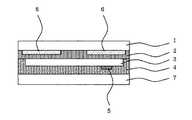
本発明のICタグを図面に基づいて説明する。図1には、本発明のICタグの一例の概略断面図が示されている。
基材シート1は、好ましくは熱可塑性樹脂からなるシートである。熱可塑性樹脂のシートとしては、例えば、高密度ポリエチレン、中密度ポリエチレン、低密度ポリエチレン等のポリエチレン系樹脂、ポリプロピレン等のポリプロピレン系樹脂、ポリメチル−1−ペンテン/エチレン/環状オレフィン共重合体、エチレン−酢酸ビニル共重合体などのポリオレフィン系樹脂、ポリエチレンテレフタレート、ポリエチレンナフタレート、ポリブチレンテレフタレートなどのポリエステル系樹脂、ポリ塩化ビニル樹脂、ポリビニルアルコール樹脂、ポリカーボネート樹脂、ポリアミド樹脂、ポリイミド樹脂、フッ素系樹脂、またはこれらのいずれかを含む共重合体、ポリマーブレンド、ポリマーアロイなどの各種合成樹脂からなるシートが使用できるが、特に、ポリエステル系樹脂から成るシートが好ましく用いられる。基材シート1は、一軸延伸または二軸延伸されたものであってもよい。基材シート1は、単層であってもよいし、同種又は異種の2層以上の多層であってもよい。また、基材シート1は、耐水性のあるものが好ましい。耐水性があると、水に濡れても破れる等の破損が生じることがない。
基材シート1の厚みは、特に制限ないが、通常10〜250μmであればよく、好ましくは20〜100μmである。
【0006】
基材シート1と第1の接着剤層2との接着力を調節するために、基材シート1の表面を表面処理してもよい。表面処理方法としては、例えば、コロナ放電処理、化学処理、樹脂コーティング等が挙げられる。
第1の接着剤層2に使用される接着剤としては、熱溶融型接着剤、感圧型接着剤、熱硬化型接着剤など種々の接着剤が挙げられる。接着剤の種類としては、例えば、天然ゴム系接着剤、合成ゴム系接着剤、アクリル樹脂系接着剤、ポリエステル樹脂系接着剤、ポリビニルエーテル樹脂系接着剤、ウレタン樹脂系接着剤、シリコーン樹脂系接着剤などが挙げられる。
【0007】
合成ゴム系接着剤の具体例としては、スチレン−ブタジエンゴム、ポリイソブチレンゴム、イソブチレン−イソプレンゴム、イソプレンゴム、スチレン−イソプレンブロック共重合体、スチレン−ブタジエンブロック共重合体、スチレン−エチレン−ブチレンブロック共重合体、エチレン−酢酸ビニル熱可塑性エラストマーなどが挙げられる。アクリル樹脂系接着剤の具体例としては、アクリル酸、アクリル酸メチル、アクリル酸エチル、アクリル酸プロピル、アクリル酸ブチル、アクリル酸−2−エチルヘキシル、メタクリル酸メチル、メタクリル酸エチル、メタクリル酸ブチル、アクリロニトリルなどの単独重合体もしくは共重合体などが挙げられる。ポリエステル樹脂系接着剤は、多価アルコールと多塩基酸の共重合体であり、多価アルコールとしてはエチレングリコール、プロピレングリコール、ブタンジオールなどが挙げられ、多塩基酸としては、テレフタル酸、アジピン酸、マレイン酸などが挙げられる。ポリビニルエーテル樹脂系接着剤の具体例としては、ポリビニルエーテル、ポリビニルイソブチルエーテルなどが挙げられる。シリコーン樹脂系接着剤の具体例としては、ジメチルポリシロキサンなどが挙げられる。これらの接着剤は、1種単独でまたは2種以上を組み合わせて用いることができる。
これらの接着剤のうち、ポリエステル樹脂系接着剤が好ましい。
【0008】
また、上記第1の接着剤層2には、必要に応じて粘着付与剤、軟化剤、老化防止剤、填料、染料又は顔料などの着色剤などを配合することができる。粘着付与剤としては、ロジン系樹脂、テルペンフェノール樹脂、テルペン樹脂、芳香族炭化水素変性テルペン樹脂、石油樹脂、クマロン・インデン樹脂、スチレン系樹脂、フェノール系樹脂、キシレン樹脂などが挙げられる。軟化剤としては、プロセスオイル、液状ゴム、可塑剤などが挙げられる。填料としては、シリカ、タルク、クレー、炭酸カルシウムなどが挙げられる。
第1の接着剤層2の厚みは、特に制限ないが、通常3〜100μmであればよく、好ましくは5〜50μmである。
【0009】
本発明のICタグにおいては、基材シート1と第1の接着剤層2の界面には、電子回路3の両端部に相当する離れた位置に剥離剤層6が設けられている。
剥離剤層6は、電子回路3の両端部に相当する位置に設けられており、電子回路3の中央部に相当する位置に設けない。すなわち、電子回路3の中央部に相当する位置には、基材シート1の表面には第1の接着剤層2が直接積層されている。このようにすることにより、ICタグを物品に貼付後に剥がす際には、電子回路3の中央部は第1の接着剤層2に接着されたまま、基材シート1と共に剥がされ、電子回路3が切断される。
剥離剤層6は、第1の接着剤層2を介して電子回路3の外周で囲まれる面積の20〜90%を覆うように設けられることが好ましく、40〜80%を覆うように設けられることが特に好ましい。
剥離剤層6は、電子回路3の外周を超えて外側にはみ出すように、設けられることが好ましく、はみ出し巾は、特に制限ないが、1mm以上が好ましい。
【0010】
剥離剤層6の形状は、電子回路3の両端部に相当する位置に設けられる形状であればよく、三角形、四角形、五角形以上の多角形、楕円、円などの形状が好ましい(図2及び3参照)。2つの剥離剤層6の形状は、同一であってもよいし、異なってもよい。なお、2つの剥離剤層6は、完全に分離独立されていることが好ましいが、一部で連結されていてもよい.。
剥離剤層6に使用される剥離剤としては、例えば、シリコーン系樹脂、長鎖アルキル系樹脂、フッ素系樹脂等の剥離剤などが挙げられる。
剥離剤層6の厚みは、特に制限されないが、0.01〜5μmが好ましく、0.03〜1μmが特に好ましい。
【0011】
本発明のICタグにおいては、第1の接着剤層2の表面に電子回路3が設けられている。
電子回路3は、導電性物質で形成された回路である。導電性物質としては、例えば、金属箔、蒸着膜、スパッタリングによる薄膜等の金属単体等が挙げられる。金属単体としては金、銀、ニッケル、銅、アルミニウムなどが使用できる。また、導電性物質としては、金、銀、ニッケル、銅等の金属の粒子をバインダーに分散させた導電性ペーストが使用できる。
金属粒子の平均粒径は、1〜15μmが好ましく、2〜10μmが特に好ましい。バインダーとしては、例えば、ポリエステル樹脂、ポリウレタン樹脂、エポキシ樹脂、フェノール樹脂などが挙げられる。
電子回路を形成する導電性物質の層の厚みは、特に制限されないが、金属箔の場合は5〜50μm、蒸着膜やスパッタリングによる金属膜の場合は0.01〜1μm、導電ペーストの場合は5〜30μmであることが好ましい。
第1の接着剤層2上に電子回路3を形成するには、例えば、金属箔を接着剤で基材シート1に貼り合わせ、金属箔をエッチング処理して回路以外の部分を除去することにより、電子回路3を形成する方法等が挙げられる。エッチング処理は、通常のエッチング処理と同様な処理により行うことができる。また、第1の接着剤層2の表面への電子回路3の形成は、導電性ペーストを、印刷、塗布などの手段により電子回路3の形状に付着させることによっても行うことができる。
【0012】
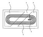
電子回路3の形状は、例えば、図2及び図3に示された形状のものが挙げられる。図2及び図3には、一本の導電性物質の線が長方形状の基材シート1の外周から内側に向けて四重の環状に所定間隔を空けて配置されてアンテナとしての電子回路3を形成している。電子回路3は、図1及び図2のように四重の環状に配置されていてもよいが、一重、二重又は三重の環状であってもよいし、五重以上の環状であってもよい。電子回路3の長さは、受信する電波の波長の長さの倍数になるように調整すればよい。
電子回路3の両末端にはICチップ5が連結されている。ICチップ5は、電子回路3の内側に設けてもよいし、電子回路3の外側に設けてもよいし、電子回路3の上部に設けてもよい。
【0013】
最外輪及び最内輪の電子回路3の末端をICチップ5と連結するためには、最外輪又は最内輪の電子回路3の末端は、その環状電子回路3と短絡することなく、飛び越えて引き出し(ジャンパ回路)、電子回路3の内側又は外側に延設し、ICチップ5と連結することが好ましい。
ジャンパ回路の形成方法は、電子回路3の末端から、その環状電子回路3の部分を横断して、絶縁インクをスクリーン印刷等により線状に印刷後、その印刷された絶縁インクの上に導電性ペーストをスクリーン印刷等により線状に印刷し、導電性回路線を形成する方法等が挙げられる。導電性ペーストは前記したものが例示される。絶縁インクとしては、紫外線硬化型インク等の光硬化型インクなどが挙げられる。
【0014】
電子回路3の末端にICチップ5を連結させる方法としては、電子回路3の末端の表面に異方性導電フィルムを介して、フリップチップボンディング法により連結する方法等が挙げられる。フリップチップボンディング法は、ICチップ5の電極部にワイヤバンプを設け、電子回路3の末端の表面に被覆された異方性導電フィルムの上に、ICチップ5のワイヤバンプがある面を押し付けて、異方性導電フィルムの中にワイヤバンプが入り込み、電子回路3の末端とICチップ5を導通し易くする方法である。
本発明のICタグにおいては、電子回路3が設けられていない第1の接着剤層2の表面、電子回路3及びICチップ5を覆うように、第2の接着剤層4が積層される。
第2の接着剤層4に使用される接着剤としては、熱溶融型接着剤、感圧型接着剤、熱硬化型接着剤など種々の接着剤が挙げられる。接着剤の種類としては、前記第1の接着剤層2に使用される接着剤と同様なものが挙げられる。これらの接着剤は、1種又は2種以上を組合せて使用することができる。これらの接着剤のうち、感圧型接着剤が好ましく、アクリル系感圧型接着剤が特に好ましい。
第2の接着剤層4の表面は平面であることが好ましい。
第2の接着剤層4の厚みは、特に制限ないが、電子回路3及びICチップ5を覆う場所と、第1の接着剤層2を覆う場所では、厚みが異なり、最大厚みは、通常10〜100μmであればよく、好ましくは15〜50μmである。
【0015】
第2の接着剤層4の表面は、剥離シート7で覆ってもよい。
剥離シート7としては、いずれのものを使用してもよく、例えば、ポリエチレンテレフタレート、ポリブチレンテレフタレート、ポリエチレン、ポリプロピレン、ポリアリレートなどの各種樹脂よりなるフィルムや、ポリエチレンラミネート紙、ポリプロピレンラミネート紙、クレーコート紙、樹脂コート紙、グラシン紙等の各種紙材を基材とし、この基材の第2の接着剤層4との接合面に、必要により剥離処理が施されたものを用いることができる。
この場合、剥離処理の代表例としては、シリコーン系樹脂、長鎖アルキル系樹脂、フッ素系樹脂等の剥離剤よりなる剥離剤層の形成が挙げられる。
剥離シート7の厚みは、特に制限されず、適宜選定すればよい。
第2の接着剤層4は、電子回路3が設けられていない第1の接着剤層2の表面、電子回路3及びICチップ5に、直接塗布、形成してもよく、また、剥離シート7の剥離剤層面に接着剤を塗布させ第2の接着剤層を形成した後、電子回路3が設けられていない第1の接着剤層2の表面、電子回路3及びICチップ5に貼り合わせてもよい。
【0016】
第1の接着剤層2、第2の接着剤層4及び剥離剤層6の形成方法としては、特に制限なく種々の方法を用いることができ、例えば、エアーナイフコーター、ブレードコーター、バーコーター、グラビアコーター、ロールコーター、カーテンコーター、ダイコーター、ナイフコーター、スクリーンコーター、マイヤーバーコーター、キスコーターなどが挙げられる。
本発明のICタグを物品に貼付した後、ICタグを剥がすと、図4に示すように、基材シート1が電子回路3を覆うように設けられている剥離剤層6との界面で剥離し、電子回路3の中央部の剥離剤層6が設けられていない基材シート1は、第2の接着剤層4、電子回路3及び第1の接着剤層2が付着したまま、物品と第2の接着剤層4との界面で剥離し、その結果、電子回路3が切断される。
なお、基材シート1の端部は、第1の接着剤層2と直接接着している場合は、基材シート1と第1の接着剤層2の界面で剥離することもあり、第1の接着剤層2の層内で剥離することもある。基材シート1の端部に直接接着している第1の接着剤層2の巾が短い場合は、基材シート1と第1の接着剤層2の界面で剥離し易いので、好ましい。
【0017】
【実施例】
次に、本発明を実施例により具体的に説明する。ただし、本発明は、これらの例によって、何ら限定されるものではない。
【0018】
(実施例1)
基材シート1としての、ポリエチレンテレフタレートフィルム(横28mm、縦12mm、厚さ50μm)の片側の表面に、図2に示すような形状(台形の斜線の角度:45度、未塗布部分の巾:3mm、2つの台形で被覆されている電子回路の外周で囲まれる面積:電子回路の外周で囲まれる面積の約75%、台形の端部と基材シート1の外縁との長さ:1mm)にシリコーン樹脂系剥離剤をグラビアコーターで乾燥して厚さ0.05μmになるように塗布し、130℃で1分間硬化させて剥離剤層6を形成した。次に、この剥離剤層6及び基材シート1の表面にポリエステル系の熱溶融型接着剤(東洋紡績(株)製、商品名「バイロン30SS」)をグラビアコーターで乾燥して厚さ5μmになるように塗布して第1の接着剤層2を積層した。さらに、この第1の接着剤層2の表面に35μm厚の電解銅箔を100℃のヒートシールロールにて加熱圧着した。次に、電解銅箔の表面に、図2のように、長辺25mm、短辺6mmの四重の環状回路(アンテナ)状に、スクリーン印刷法により、エッチングレジストインクを印刷(線幅:0.3mm)した。これを塩化第二鉄溶液にてエッチクング処理を行い、回路以外の部分を除去した。この後、アルカリ水溶液にてエッチングレジストインクを除去し、電子回路3を形成した。
【0019】
最内輪の電子回路(アンテナ)3の末端と、その最外輪の電子回路3の末端を導通させるために、それらの間を紫外線硬化型インクをスクリーン印刷法により線状に印刷後、紫外線を照射して硬化させ、その紫外線硬化型インクの硬化線の表面に銀ペースト(銀粒子の平均粒径:5μm、バインダー:ポリエステル樹脂)をスクリーン印刷法により線状(長さ10mm)に印刷し、乾燥させ、ジャンパ回路を形成した。
次いで、ICチップ(フィリップス社製、商品名「I/CODE」)5の電極部に金線を用いてワイヤバンプを設け、このICチップ5を異方性導電フィルム(ソニーケミカル社製、商品名「FP2322D」)を介して、回路の両末端に、フリップチップボンディング法を用いて、連結した。
一方、厚さ70μmのグラシン紙の片側全面にシリコーン樹脂により剥離処理した剥離紙の剥離処理面に、ロールナイフコーターを用いて、アクリル系低接着性感圧型接着剤(リンテック(株)製、商品名「PA−T1」)を塗布、乾燥して厚さ20μmの第2の接着剤層4を形成した第2の接着剤層4付き剥離紙を用意した。
次に、電子回路3及びICチップ5が設けられた基材シート1の表面の全体に、第2の接着剤層4付き剥離紙7の第2の接着剤層4を貼り合わせ、第1の接着剤層2、電子回路3及びICチップ5を第2の接着剤層4で被覆し、ICタグを作成した。
【0020】
得られたICタグについて、非接触送受信試験を行ったところ、正常に送受信を行うことができた。
このICタグの全面処理剥離紙を剥がし、ポリプロピレン樹脂板に貼付した。24時間後、このICタグをポリプロピレン樹脂板から剥離させたところ、剥離剤層6で覆われた電子回路3の部分がポリプロピレン樹脂板に残留し、それ以外の非剥離剤層部分は基材シート1のポリエチレンテレフタレートシートと共に、ポリプロピレン樹脂板から剥離された。その剥離に伴い電子回路3が切断され、非接触送受信試験を行ったところ、送受信を行うことができなかった。
【0021】
(比較例1)
剥離剤層6を設けなかった以外は、実施例1と同様にしてICタグを作成した。
得られたICタグについて、非接触送受信試験を行ったところ、正常に送受信を行うことができた。
このICタグについて、実施例1と同様にポリプロピレン樹脂板に貼付し、剥離させたところ、電子回路3を破壊することもなく、容易に剥離させることが可能であった。この剥離後のICタグについて、非接触送受信試験を行ったところ、正常に送受信を行うことができた。
【0022】
【発明の効果】
本発明のICタグは、物品に貼付された後に剥がした場合、内蔵している電子回路を確実に破損することができる。
【図面の簡単な説明】
【図1】 本発明のICタグの一例の概略断面図である。
【図2】 本発明のICタグの一例の電子回路を示す平面図である。
【図3】 本発明のICタグの他の一例の電子回路を示す平面図である。
【図4】 本発明のICタグが剥がされた後の一例の断面図である。
【符号の説明】
1 基材シート
2 第1の接着剤層
3 電子回路
4 第2の接着剤層
5 ICチップ
6 剥離剤層
7 剥離シート
8 物品[0001]
[Technical field to which the invention belongs]
The present invention relates to an IC tag capable of damaging a built-in electronic circuit when peeled off after being attached to an article.
[0002]
[Prior art]
In recent years, an IC tag is attached to an article such as a product, a stored item, or a baggage to manage the article. For example, an IC tag on which information such as manufacturing conditions, purchase status, price information, and usage status is recorded is attached to the product, and the recorded information is checked and managed by an interrogator (interrogator) as necessary. To be done.
However, when the adhesive force of the adhesive used for the IC tag attached to the article is not sufficient, it may be replaced with another article for some reason such as error or carelessness. In some cases, it may be intentionally attached to another article.
In such a situation, the article management can no longer be performed accurately.
[0003]
[Problems to be solved by the invention]
As a method for solving the above problems, there is a demand for accurate management of an article so that the function of the IC tag is impaired when it is attached to another article.
[0004]
[Means for Solving the Problems]
As a result of intensive studies to solve the above problems, the present inventors have laminated a first adhesive layer on a base sheet, provided an electronic circuit and an IC chip that connects both ends of the electronic circuit, A second adhesive layer to be covered is laminated, and a release agent layer is provided ata position corresponding to both ends of the electronic circuit at the interface between the base sheet and the first adhesive layer, anda central portion of theelectronic circuit. the position corresponding to, without providing the release agent layer, by Rukotoon the surface of the substrate sheet is laminated first adhesive layer directly, found the above problems can be solved, and have completed the present invention .
That is, according to the present invention, a first adhesive layer is laminated on the surface of a base sheet, and an electronic circuit and an IC chip that connects both ends of the electronic circuit are provided on the surface of the adhesive layer. And a second adhesive layer covering the IC chip, and a release agent layer ata position corresponding to both ends of the electronic circuit at the interface between the base sheet and the first adhesive layer. An IC tagis provided, wherein a release agent layer is not provided at a position corresponding to a central portion of an electronic circuit, and a first adhesive layer is directly laminated on a surface of a base sheet. It is to provide.
In addition, the present invention provides an IC tag in which the release agent layer is provided so as to protrude outward beyond the outer periphery of the electronic circuit, and the protruding width is 1 mm or more.
The present invention also provides the IC tag, wherein the release agent layer is provided so as to cover 20 to 90% of the area surrounded by the outer periphery of the electronic circuit via the first adhesive layer. To do.
The present invention also provides an IC tag in which a release sheet is laminated on the surface of the second adhesive layer in the IC tag.
[0005]
DETAILED DESCRIPTION OF THE INVENTION
The IC tag of the present invention will be described with reference to the drawings. FIG. 1 shows a schematic cross-sectional view of an example of an IC tag of the present invention.
The base sheet 1 is preferably a sheet made of a thermoplastic resin. Examples of the thermoplastic resin sheet include polyethylene resins such as high density polyethylene, medium density polyethylene, and low density polyethylene, polypropylene resins such as polypropylene, polymethyl-1-pentene / ethylene / cycloolefin copolymer, ethylene- Polyolefin resins such as vinyl acetate copolymer, polyester resins such as polyethylene terephthalate, polyethylene naphthalate, polybutylene terephthalate, polyvinyl chloride resin, polyvinyl alcohol resin, polycarbonate resin, polyamide resin, polyimide resin, fluorine resin, or Sheets made of various synthetic resins such as copolymers, polymer blends, and polymer alloys containing any of these can be used. In particular, sheets made of polyester resins are preferably used. It is. The base sheet 1 may be uniaxially stretched or biaxially stretched. The base sheet 1 may be a single layer or a multilayer of two or more layers of the same type or different types. The base sheet 1 is preferably water resistant. If it is water resistant, it will not break even if it gets wet.
Although the thickness in particular of the base material sheet 1 does not have a restriction | limiting, Usually, what is necessary is just 10-250 micrometers, Preferably it is 20-100 micrometers.
[0006]
In order to adjust the adhesive force between the base sheet 1 and the first
Examples of the adhesive used for the first
[0007]
Specific examples of the synthetic rubber adhesive include styrene-butadiene rubber, polyisobutylene rubber, isobutylene-isoprene rubber, isoprene rubber, styrene-isoprene block copolymer, styrene-butadiene block copolymer, styrene-ethylene-butylene block. Examples thereof include copolymers and ethylene-vinyl acetate thermoplastic elastomers. Specific examples of acrylic resin adhesives include acrylic acid, methyl acrylate, ethyl acrylate, propyl acrylate, butyl acrylate, 2-ethylhexyl acrylate, methyl methacrylate, ethyl methacrylate, butyl methacrylate, acrylonitrile Homopolymers or copolymers such as The polyester resin adhesive is a copolymer of a polyhydric alcohol and a polybasic acid. Examples of the polyhydric alcohol include ethylene glycol, propylene glycol, and butanediol. Polybasic acids include terephthalic acid and adipic acid. And maleic acid. Specific examples of the polyvinyl ether resin adhesive include polyvinyl ether and polyvinyl isobutyl ether. Specific examples of the silicone resin adhesive include dimethylpolysiloxane. These adhesives can be used individually by 1 type or in combination of 2 or more types.
Of these adhesives, polyester resin adhesives are preferred.
[0008]
The first
Although the thickness of the 1st
[0009]
In the IC tag of the present invention, a
The
The
The
[0010]
The shape of the
Examples of the release agent used in the
The thickness of the
[0011]
In the IC tag of the present invention, the
The
1-15 micrometers is preferable and, as for the average particle diameter of a metal particle, 2-10 micrometers is especially preferable. Examples of the binder include polyester resin, polyurethane resin, epoxy resin, phenol resin, and the like.
The thickness of the conductive material layer forming the electronic circuit is not particularly limited, but is 5 to 50 μm for a metal foil, 0.01 to 1 μm for a deposited film or a metal film formed by sputtering, and 5 for a conductive paste. It is preferable that it is -30 micrometers.
In order to form the
[0012]
Examples of the shape of the
An
[0013]
In order to connect the end of the
The method of forming the jumper circuit is that the insulating ink is printed in a line shape by screen printing or the like across the annular
[0014]
Examples of the method of connecting the
In the IC tag of the present invention, the second adhesive layer 4 is laminated so as to cover the surface of the first
Examples of the adhesive used for the second adhesive layer 4 include various adhesives such as a hot-melt adhesive, a pressure-sensitive adhesive, and a thermosetting adhesive. As a kind of adhesive agent, the thing similar to the adhesive agent used for the said 1st
The surface of the second adhesive layer 4 is preferably a flat surface.
The thickness of the second adhesive layer 4 is not particularly limited, but the thickness is different between the place covering the
[0015]
The surface of the second adhesive layer 4 may be covered with a
Any
In this case, a typical example of the release treatment includes formation of a release agent layer made of a release agent such as a silicone resin, a long-chain alkyl resin, or a fluorine resin.
The thickness of the
The second adhesive layer 4 may be directly applied and formed on the surface of the first
[0016]
As a method for forming the first
When the IC tag of the present invention is attached to an article and then peeled off, the substrate sheet 1 is peeled off at the interface with the
In addition, when the edge part of the base material sheet 1 is directly adhere | attaching with the 1st
[0017]
【Example】
Next, the present invention will be specifically described with reference to examples. However, the present invention is not limited by these examples.
[0018]
(Example 1)
On the surface of one side of a polyethylene terephthalate film (width 28 mm, length 12 mm, thickness 50 μm) as the base sheet 1, a shape as shown in FIG. 2 (angle of trapezoidal diagonal lines: 45 degrees, width of uncoated part: 3 mm, area surrounded by the outer periphery of the electronic circuit covered with two trapezoids: about 75% of the area surrounded by the outer periphery of the electronic circuit, the length of the end of the trapezoid and the outer edge of the base sheet 1: 1 mm) A silicone resin release agent was dried on a gravure coater to a thickness of 0.05 μm and cured at 130 ° C. for 1 minute to form a
[0019]
In order to make the end of the innermost ring electronic circuit (antenna) 3 and the end of the outermost ring
Next, wire bumps are provided on the electrode part of the IC chip (manufactured by Philips, trade name “I / CODE”) 5 using a gold wire, and the
On the other hand, an acrylic low-adhesive pressure-sensitive adhesive (trade name, manufactured by Lintec Co., Ltd.) was used on the release-treated surface of the release paper obtained by releasing the entire surface of one side of a glassine paper having a thickness of 70 μm with a silicone resin. A release paper with a second adhesive layer 4 in which a second adhesive layer 4 having a thickness of 20 μm was formed by applying and drying “PA-T1”) was prepared.
Next, the second adhesive layer 4 of the
[0020]
When the obtained IC tag was subjected to a non-contact transmission / reception test, the transmission / reception was successfully performed.
The entire surface treated release paper of this IC tag was peeled off and attached to a polypropylene resin plate. After 24 hours, when this IC tag was peeled from the polypropylene resin plate, the portion of the
[0021]
(Comparative Example 1)
An IC tag was prepared in the same manner as in Example 1 except that the
When the obtained IC tag was subjected to a non-contact transmission / reception test, the transmission / reception was successfully performed.
When this IC tag was affixed to a polypropylene resin plate and peeled off in the same manner as in Example 1, the
[0022]
【The invention's effect】
When the IC tag of the present invention is peeled off after being attached to an article, the built-in electronic circuit can be reliably damaged.
[Brief description of the drawings]
FIG. 1 is a schematic cross-sectional view of an example of an IC tag of the present invention.
FIG. 2 is a plan view showing an electronic circuit of an example of an IC tag of the present invention.
FIG. 3 is a plan view showing an electronic circuit of another example of the IC tag of the present invention.
FIG. 4 is a cross-sectional view of an example after the IC tag of the present invention is peeled off.
[Explanation of symbols]
DESCRIPTION OF SYMBOLS 1
Claims (4)
Translated fromJapanesePriority Applications (8)
| Application Number | Priority Date | Filing Date | Title |
|---|---|---|---|
| JP2002140535AJP4342771B2 (en) | 2002-05-15 | 2002-05-15 | IC tag |
| CNA038110164ACN1653485A (en) | 2002-05-15 | 2003-05-14 | IC tag |
| EP03741114AEP1505537B1 (en) | 2002-05-15 | 2003-05-14 | Ic tag |
| US10/514,495US7540427B2 (en) | 2002-05-15 | 2003-05-14 | IC tag |
| TW092113061ATWI329282B (en) | 2002-05-15 | 2003-05-14 | Ic tag |
| KR1020047018113AKR100921863B1 (en) | 2002-05-15 | 2003-05-14 | IC tag |
| DE60309860TDE60309860T2 (en) | 2002-05-15 | 2003-05-14 | IC LABEL |
| PCT/JP2003/006026WO2003098545A1 (en) | 2002-05-15 | 2003-05-14 | Ic tag |
Applications Claiming Priority (1)
| Application Number | Priority Date | Filing Date | Title |
|---|---|---|---|
| JP2002140535AJP4342771B2 (en) | 2002-05-15 | 2002-05-15 | IC tag |
Publications (2)
| Publication Number | Publication Date |
|---|---|
| JP2003331248A JP2003331248A (en) | 2003-11-21 |
| JP4342771B2true JP4342771B2 (en) | 2009-10-14 |
Family
ID=29544927
Family Applications (1)
| Application Number | Title | Priority Date | Filing Date |
|---|---|---|---|
| JP2002140535AExpired - Fee RelatedJP4342771B2 (en) | 2002-05-15 | 2002-05-15 | IC tag |
Country Status (8)
| Country | Link |
|---|---|
| US (1) | US7540427B2 (en) |
| EP (1) | EP1505537B1 (en) |
| JP (1) | JP4342771B2 (en) |
| KR (1) | KR100921863B1 (en) |
| CN (1) | CN1653485A (en) |
| DE (1) | DE60309860T2 (en) |
| TW (1) | TWI329282B (en) |
| WO (1) | WO2003098545A1 (en) |
Families Citing this family (23)
| Publication number | Priority date | Publication date | Assignee | Title |
|---|---|---|---|---|
| US7633145B2 (en) | 2004-01-16 | 2009-12-15 | Semiconductor Energy Laboratory Co., Ltd. | Semiconductor device with antenna and separating layer |
| WO2005083661A1 (en)* | 2004-02-27 | 2005-09-09 | Nippon Carbide Kogyo Kabushiki Kaisha | Display device with theft prevention structure |
| JP4529486B2 (en)* | 2004-03-04 | 2010-08-25 | 凸版印刷株式会社 | Non-contact IC media |
| JP4354317B2 (en)* | 2004-03-25 | 2009-10-28 | リンテック株式会社 | IC tag and manufacturing method thereof |
| JP4590908B2 (en)* | 2004-04-09 | 2010-12-01 | 凸版印刷株式会社 | Non-contact IC medium and method of manufacturing non-contact IC medium |
| WO2005104026A1 (en)* | 2004-04-23 | 2005-11-03 | Konica Minolta Photo Imaging, Inc. | Ic card and method of producing the same |
| JP4549765B2 (en)* | 2004-07-22 | 2010-09-22 | 大日本印刷株式会社 | Non-contact data carrier with break detection function |
| JP4675184B2 (en)* | 2004-10-29 | 2011-04-20 | リンテック株式会社 | IC tag |
| JP2006134249A (en)* | 2004-11-09 | 2006-05-25 | Fujitsu Ltd | RFID tag |
| JP2006324075A (en)* | 2005-05-18 | 2006-11-30 | Matsushita Electric Ind Co Ltd | Battery pack |
| EP2013821B1 (en)* | 2006-04-10 | 2011-10-12 | Innovatier, Inc. | An electronic inlay module for electronic cards and tags, electronic card and methods for manufacturing such electronic inlay modules and cards |
| JP2007286193A (en)* | 2006-04-13 | 2007-11-01 | Brother Ind Ltd | Tag tape and RFID label |
| WO2008067830A1 (en)* | 2006-12-05 | 2008-06-12 | Hueck Folien Ges.M.B.H. | Manipulation-proof rfid antenna |
| JP2009075712A (en)* | 2007-09-19 | 2009-04-09 | Toppan Printing Co Ltd | IC label for forgery prevention |
| KR20110002837A (en)* | 2008-04-24 | 2011-01-10 | 도레이 카부시키가이샤 | Contactless IC Tag |
| PL2164032T3 (en)* | 2008-09-15 | 2019-01-31 | Hueck Folien Ges.M.B.H. | Manipulation-proof RFID antenna with safety feature |
| JP5220654B2 (en)* | 2009-02-24 | 2013-06-26 | 富士通株式会社 | RFID tag |
| DE102010005714B4 (en)* | 2010-01-26 | 2019-03-14 | Schreiner Group Gmbh & Co. Kg | Safety tag, arrangement with a safety tag and method of operating a safety tag |
| JP6073048B2 (en)* | 2011-07-04 | 2017-02-01 | 東洋アルミニウム株式会社 | RFID inlet antenna and RFID using the same |
| CN103971590B (en)* | 2013-02-01 | 2017-02-22 | 比亚迪股份有限公司 | Anti-counterfeiting trademark and manufacturing method thereof |
| JP2015060504A (en)* | 2013-09-20 | 2015-03-30 | 凸版印刷株式会社 | Non-contact IC label |
| JP6673022B2 (en)* | 2016-05-31 | 2020-03-25 | 富士通株式会社 | Electronic devices and beacons |
| JP2023000121A (en)* | 2021-06-17 | 2023-01-04 | 凸版印刷株式会社 | packaging material |
Family Cites Families (21)
| Publication number | Priority date | Publication date | Assignee | Title |
|---|---|---|---|---|
| US4717438A (en)* | 1986-09-29 | 1988-01-05 | Monarch Marking Systems, Inc. | Method of making tags |
| US5108819A (en)* | 1990-02-14 | 1992-04-28 | Eli Lilly And Company | Thin film electrical component |
| US5131686A (en)* | 1990-09-20 | 1992-07-21 | Carlson Thomas S | Method for producing identification cards |
| US5142270A (en)* | 1991-05-22 | 1992-08-25 | Checkpoint Systems Inc. | Stabilized resonant tag circuit and deactivator |
| US5767772A (en)* | 1993-12-15 | 1998-06-16 | Lemaire; Gerard | Marker for an article which is detected when it passes through a surveillance zone |
| US5528222A (en)* | 1994-09-09 | 1996-06-18 | International Business Machines Corporation | Radio frequency circuit and memory in thin flexible package |
| US6270871B1 (en)* | 1996-09-27 | 2001-08-07 | Avery Dennison Corporation | Overlaminated pressure-sensitive adhesive construction |
| US5884425A (en)* | 1997-05-23 | 1999-03-23 | Avery Dennison Corporation | Anti-tamper tag with theft protection |
| JP3853480B2 (en)* | 1997-09-05 | 2006-12-06 | 大日本印刷株式会社 | Non-contact IC card |
| JP4046167B2 (en)* | 1998-08-12 | 2008-02-13 | リンテック株式会社 | Non-contact data carrier label |
| JP2000105806A (en)* | 1998-09-29 | 2000-04-11 | Toshiba Chem Corp | Label type noncontact data carrier |
| US6147604A (en)* | 1998-10-15 | 2000-11-14 | Intermec Ip Corporation | Wireless memory device |
| US6262692B1 (en)* | 1999-01-13 | 2001-07-17 | Brady Worldwide, Inc. | Laminate RFID label and method of manufacture |
| JP4095741B2 (en)* | 1999-06-29 | 2008-06-04 | シチズンミヨタ株式会社 | IC tag structure |
| JP4117989B2 (en)* | 1999-12-10 | 2008-07-16 | シチズンミヨタ株式会社 | IC tag |
| JP3557981B2 (en)* | 2000-01-17 | 2004-08-25 | ソニーケミカル株式会社 | Information recording tag |
| ES2351549T3 (en)* | 2000-03-21 | 2011-02-07 | Mikoh Corporation | A RADIO FREQUENCY IDENTIFICATION LABEL WITH INDICATION OF INDEBIT HANDLING. |
| US7049962B2 (en)* | 2000-07-28 | 2006-05-23 | Micoh Corporation | Materials and construction for a tamper indicating radio frequency identification label |
| JP2002222403A (en)* | 2001-01-25 | 2002-08-09 | Konica Corp | Ic-mounted card base material, ic-mounted individual identifying card and its manufacturing method |
| US6830193B2 (en)* | 2001-11-29 | 2004-12-14 | Matsushita Electric Industrial Co., Ltd. | Non-contact IC card |
| JP2003302907A (en)* | 2002-04-12 | 2003-10-24 | Matsushita Electric Ind Co Ltd | sticker |
- 2002
- 2002-05-15JPJP2002140535Apatent/JP4342771B2/ennot_activeExpired - Fee Related
- 2003
- 2003-05-14KRKR1020047018113Apatent/KR100921863B1/ennot_activeExpired - Fee Related
- 2003-05-14TWTW092113061Apatent/TWI329282B/ennot_activeIP Right Cessation
- 2003-05-14CNCNA038110164Apatent/CN1653485A/enactivePending
- 2003-05-14WOPCT/JP2003/006026patent/WO2003098545A1/enactiveIP Right Grant
- 2003-05-14EPEP03741114Apatent/EP1505537B1/ennot_activeExpired - Lifetime
- 2003-05-14DEDE60309860Tpatent/DE60309860T2/ennot_activeExpired - Lifetime
- 2003-05-14USUS10/514,495patent/US7540427B2/ennot_activeExpired - Fee Related
Also Published As
| Publication number | Publication date |
|---|---|
| DE60309860D1 (en) | 2007-01-04 |
| CN1653485A (en) | 2005-08-10 |
| EP1505537A1 (en) | 2005-02-09 |
| US7540427B2 (en) | 2009-06-02 |
| TW200407810A (en) | 2004-05-16 |
| KR20040104727A (en) | 2004-12-10 |
| JP2003331248A (en) | 2003-11-21 |
| KR100921863B1 (en) | 2009-10-13 |
| US20060273179A1 (en) | 2006-12-07 |
| WO2003098545A1 (en) | 2003-11-27 |
| EP1505537A4 (en) | 2005-09-14 |
| EP1505537B1 (en) | 2006-11-22 |
| DE60309860T2 (en) | 2007-09-13 |
| TWI329282B (en) | 2010-08-21 |
Similar Documents
| Publication | Publication Date | Title |
|---|---|---|
| JP4342771B2 (en) | IC tag | |
| US9048525B2 (en) | Antenna circuit | |
| KR20010089216A (en) | Information recording tag | |
| JP2008123083A (en) | Non-contact IC tag label, air baggage tag label, and non-contact IC tag label manufacturing method | |
| JP2003150924A (en) | Non-contact ic label | |
| KR100973877B1 (en) | IC tag | |
| JP5248224B2 (en) | Electronic circuit and IC tag | |
| JP4127650B2 (en) | IC tag | |
| JP4339069B2 (en) | IC tag | |
| JP3956660B2 (en) | Non-contact type IC tag and method for manufacturing non-contact type IC tag | |
| WO2008047705A1 (en) | Ic tag label | |
| JP2003167515A (en) | Rfid tag for managing ink cartridge and ink cartridge attached with the same | |
| JP4350093B2 (en) | Flip chip mounting board | |
| JP4354317B2 (en) | IC tag and manufacturing method thereof | |
| JP4848214B2 (en) | Non-contact IC tag | |
| CN100367308C (en) | IC tag | |
| JP2005055975A (en) | Ic tag | |
| JP4078086B2 (en) | Adhesive sheet assembly | |
| JP2004317544A (en) | Label with IC chip mount | |
| JP2007004818A (en) | Non-contact ic tag and method for manufacturing non-contact ic tag |
Legal Events
| Date | Code | Title | Description |
|---|---|---|---|
| A621 | Written request for application examination | Free format text:JAPANESE INTERMEDIATE CODE: A621 Effective date:20050331 | |
| A131 | Notification of reasons for refusal | Free format text:JAPANESE INTERMEDIATE CODE: A131 Effective date:20080812 | |
| A521 | Written amendment | Free format text:JAPANESE INTERMEDIATE CODE: A523 Effective date:20080926 | |
| TRDD | Decision of grant or rejection written | ||
| A01 | Written decision to grant a patent or to grant a registration (utility model) | Free format text:JAPANESE INTERMEDIATE CODE: A01 Effective date:20090707 | |
| A01 | Written decision to grant a patent or to grant a registration (utility model) | Free format text:JAPANESE INTERMEDIATE CODE: A01 | |
| A61 | First payment of annual fees (during grant procedure) | Free format text:JAPANESE INTERMEDIATE CODE: A61 Effective date:20090708 | |
| FPAY | Renewal fee payment (event date is renewal date of database) | Free format text:PAYMENT UNTIL: 20120717 Year of fee payment:3 | |
| R150 | Certificate of patent or registration of utility model | Free format text:JAPANESE INTERMEDIATE CODE: R150 | |
| FPAY | Renewal fee payment (event date is renewal date of database) | Free format text:PAYMENT UNTIL: 20120717 Year of fee payment:3 | |
| FPAY | Renewal fee payment (event date is renewal date of database) | Free format text:PAYMENT UNTIL: 20130717 Year of fee payment:4 | |
| R250 | Receipt of annual fees | Free format text:JAPANESE INTERMEDIATE CODE: R250 | |
| R250 | Receipt of annual fees | Free format text:JAPANESE INTERMEDIATE CODE: R250 | |
| R250 | Receipt of annual fees | Free format text:JAPANESE INTERMEDIATE CODE: R250 | |
| LAPS | Cancellation because of no payment of annual fees |