JP4340246B2 - Thin film solar cell and manufacturing method thereof - Google Patents
Thin film solar cell and manufacturing method thereofDownload PDFInfo
- Publication number
- JP4340246B2 JP4340246B2JP2005062816AJP2005062816AJP4340246B2JP 4340246 B2JP4340246 B2JP 4340246B2JP 2005062816 AJP2005062816 AJP 2005062816AJP 2005062816 AJP2005062816 AJP 2005062816AJP 4340246 B2JP4340246 B2JP 4340246B2
- Authority
- JP
- Japan
- Prior art keywords
- transparent conductive
- solar cell
- conductive film
- photoelectric conversion
- groove
- Prior art date
- Legal status (The legal status is an assumption and is not a legal conclusion. Google has not performed a legal analysis and makes no representation as to the accuracy of the status listed.)
- Expired - Fee Related
Links
Images


Classifications
- H—ELECTRICITY
- H10—SEMICONDUCTOR DEVICES; ELECTRIC SOLID-STATE DEVICES NOT OTHERWISE PROVIDED FOR
- H10F—INORGANIC SEMICONDUCTOR DEVICES SENSITIVE TO INFRARED RADIATION, LIGHT, ELECTROMAGNETIC RADIATION OF SHORTER WAVELENGTH OR CORPUSCULAR RADIATION
- H10F19/00—Integrated devices, or assemblies of multiple devices, comprising at least one photovoltaic cell covered by group H10F10/00, e.g. photovoltaic modules
- H10F19/30—Integrated devices, or assemblies of multiple devices, comprising at least one photovoltaic cell covered by group H10F10/00, e.g. photovoltaic modules comprising thin-film photovoltaic cells
- H10F19/31—Integrated devices, or assemblies of multiple devices, comprising at least one photovoltaic cell covered by group H10F10/00, e.g. photovoltaic modules comprising thin-film photovoltaic cells having multiple laterally adjacent thin-film photovoltaic cells deposited on the same substrate
- H10F19/33—Patterning processes to connect the photovoltaic cells, e.g. laser cutting of conductive or active layers
- H—ELECTRICITY
- H10—SEMICONDUCTOR DEVICES; ELECTRIC SOLID-STATE DEVICES NOT OTHERWISE PROVIDED FOR
- H10F—INORGANIC SEMICONDUCTOR DEVICES SENSITIVE TO INFRARED RADIATION, LIGHT, ELECTROMAGNETIC RADIATION OF SHORTER WAVELENGTH OR CORPUSCULAR RADIATION
- H10F19/00—Integrated devices, or assemblies of multiple devices, comprising at least one photovoltaic cell covered by group H10F10/00, e.g. photovoltaic modules
- H10F19/30—Integrated devices, or assemblies of multiple devices, comprising at least one photovoltaic cell covered by group H10F10/00, e.g. photovoltaic modules comprising thin-film photovoltaic cells
- H10F19/31—Integrated devices, or assemblies of multiple devices, comprising at least one photovoltaic cell covered by group H10F10/00, e.g. photovoltaic modules comprising thin-film photovoltaic cells having multiple laterally adjacent thin-film photovoltaic cells deposited on the same substrate
- H10F19/37—Integrated devices, or assemblies of multiple devices, comprising at least one photovoltaic cell covered by group H10F10/00, e.g. photovoltaic modules comprising thin-film photovoltaic cells having multiple laterally adjacent thin-film photovoltaic cells deposited on the same substrate comprising means for obtaining partial light transmission through the integrated devices, or the assemblies of multiple devices, e.g. partially transparent thin-film photovoltaic modules for windows
- Y—GENERAL TAGGING OF NEW TECHNOLOGICAL DEVELOPMENTS; GENERAL TAGGING OF CROSS-SECTIONAL TECHNOLOGIES SPANNING OVER SEVERAL SECTIONS OF THE IPC; TECHNICAL SUBJECTS COVERED BY FORMER USPC CROSS-REFERENCE ART COLLECTIONS [XRACs] AND DIGESTS
- Y02—TECHNOLOGIES OR APPLICATIONS FOR MITIGATION OR ADAPTATION AGAINST CLIMATE CHANGE
- Y02E—REDUCTION OF GREENHOUSE GAS [GHG] EMISSIONS, RELATED TO ENERGY GENERATION, TRANSMISSION OR DISTRIBUTION
- Y02E10/00—Energy generation through renewable energy sources
- Y02E10/50—Photovoltaic [PV] energy
Landscapes
- Photovoltaic Devices (AREA)
Description
Translated fromJapanese本発明は薄膜太陽電池およびその製造方法に関し、特に歩留りが高く、光電変換層に短絡が生じた場合でも変換効率の低下を抑制することができる薄膜太陽電池とその製造方法に関する。 The present invention relates to a thin film solar cell and a method for manufacturing the same, and more particularly to a thin film solar cell having a high yield and capable of suppressing a decrease in conversion efficiency even when a short circuit occurs in a photoelectric conversion layer.
図7に、従来の薄膜太陽電池の一部の模式的な斜視断面図を示す。この薄膜太陽電池においては、ガラス基板などの絶縁透光性基板1上に短冊状の透明導電膜2が形成されており、この透明導電膜2上に公知のプラズマCVD法などにより順次積層されたアモルファスシリコン薄膜からなるp層、i層およびn層からなる短冊状の光電変換層3と、裏面電極4とを含む太陽電池セル10、11が形成されている。また、透明導電膜2は第1分離溝5によって分離されており、光透過用の第1開口溝7を挟んで第1太陽電池セル10と第2太陽電池セル11とが隣接し、第1太陽電池セル10の透明導電膜2と第2太陽電池セル11の裏面電極4とが接続用溝6を介して電気的に直列に接続されている。 FIG. 7 shows a schematic perspective sectional view of a part of a conventional thin film solar cell. In this thin film solar cell, a strip-like transparent
このような構成の薄膜太陽電池は、絶縁透光性基板1によってその表面の保護を図ることができ、またSnO2などの耐プラズマ性透明導電膜が開発され、プラズマCVD法によるアモルファスシリコン薄膜の生成が可能になったことから、多用されるようになり、現在の主流となっている。The surface of the thin-film solar cell having such a structure can be protected by the insulating
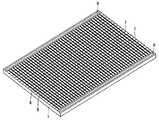
図6の模式的斜視図に、図7に示す薄膜太陽電池の外観を示す。このような薄膜太陽電池においては、光の透過性をさらに向上させるために、図3の模式的斜視図に示すように、第1開口溝7と直交する第2開口溝8をさらに設けることができる。この図3に示す薄膜太陽電池においては、導線9によって電流が取り出される。
図6および図7に示すような薄膜太陽電池は、たとえば特許文献1に開示されているが、光電変換層に短絡が生じた場合には、その短絡箇所に光電流が集中しやすくなるため、透明導電膜によって複数の太陽電池セルが直列に接続されている図6および図7に示す薄膜太陽電池全体の変換効率が大きく低下するという問題があった。 Although the thin film solar cell as shown in FIG. 6 and FIG. 7 is disclosed in, for example,
そこで、たとえば特許文献2には、図3に示す構造の薄膜太陽電池において、第2開口溝8を挟んで隣接する太陽電池セルの間の透明導電膜をすべて分離することにより、太陽電池セルの光電変換層に短絡が生じた場合でも薄膜太陽電池全体の変換効率の低下に与える影響を少なくする方法が開示されている。しかしながら、特許文献2の方法おいては、レーザスクライブに用いられるYAG(Yttrium-Aluminum-Garnet)基本波レーザ光の出力を微妙に調整し透明導電膜の昇華による残渣を残さないようにして透明導電膜、光電変換層および裏面電極を一度に分離して第2開口溝を形成しているが、YAG基本波レーザ光の出力の調整が難しいため加工条件が非常に厳しく、歩留りが悪くなるという問題があった。すなわち、透明導電膜、光電変換層および裏面電極を一度に分離することができるYAG基本波レーザ光の条件は非常に厳しいため第2開口溝の形成が非常に困難であり、YAG基本波レーザ光の出力が高すぎると昇華した透明導電膜が再付着して短絡を生じ、低すぎると第2開口溝を形成することができない。また、予め透明導電膜をYAG基本波レーザ光を用いたレーザスクライブにより分離しておき、光電変換層の形成後に可視レーザ光で光電変換層を分離する方法も考えられるが、加工時間が長くなり、異なるレーザ加工装置で細い分離線を一致させるように位置合わせするのが非常に難しい。 Therefore, for example, in
上記の事情に鑑みて、本発明の目的は、歩留りが高く、光電変換層に短絡が生じた場合でも変換効率の低下を抑制することができる薄膜太陽電池とその製造方法を提供することにある。 In view of the above circumstances, an object of the present invention is to provide a thin-film solar cell that has a high yield and can suppress a decrease in conversion efficiency even when a short circuit occurs in the photoelectric conversion layer, and a method for manufacturing the same. .
本発明は、絶縁透光性基板上に設置された透明導電膜と、絶縁透光性基板上において互いに直交し透明導電膜を複数に分離している、第1分離溝と、第2分離溝と、絶縁透光性基板上において互いに直交している、第1分離溝に平行な少なくとも1本の第1開口溝と、第2分離溝に平行な少なくとも2本の第2開口溝と、を含み、第1開口溝を挟んで隣接する位置および第2開口溝を挟んで隣接する位置のそれぞれに絶縁透光性基板上に形成された、光電変換層と、裏面電極と、を含む太陽電池セルが設置されており、第1開口溝を挟んで隣接している一対の太陽電池セルにおいては、一方の太陽電池セルの光電変換層と他方の太陽電池セルの裏面電極とがそれぞれ透明導電膜と接触することによって電気的に接続され、第2開口溝を挟んで隣接している一対の太陽電池セルにおいては、一方の太陽電池セルの光電変換層に接触している透明導電膜と他方の太陽電池セルの光電変換層に接触している透明導電膜とが第2分離溝により分離されておらず電気的に接続されているものと、一方の太陽電池セルの光電変換層に接触している透明導電膜と他方の太陽電池セルの光電変換層に接触している透明導電膜とが第2分離溝により分離されており電気的に絶縁されているものとが混在しており、透明導電膜を分離している第2分離溝が所定の間隔で配置されている薄膜太陽電池である。The present invention relates to a transparent conductive film installed on an insulating translucent substrate, and a first separation groove and a second separation groove which are orthogonal to each other and separate the transparent conductive film into a plurality of parts on the insulating translucent substrate. And at least one first opening groove parallel to the first separation groove and at least two second opening grooves parallel to the second separation groove, which are orthogonal to each other on the insulating translucent substrate. A solar cell including a photoelectric conversion layer and a back electrode formed on the insulating translucent substrate at positions adjacent to each other with the first opening groove interposed therebetween and positions adjacent to each other with the second opening groove interposed therebetween In the pair of solar cells adjacent to each other with the first opening groove interposed, the photoelectric conversion layer of one solar cell and the back electrode of the other solar cell are respectively transparent conductive films. Is electrically connected by contacting with the second opening groove In the pair of solar cells in contact with each other, the transparent conductive film in contact with the photoelectric conversion layer of one solar cell and the transparent conductive film in contact with the photoelectric conversion layer of the other solar cell are second. It is not separated by the separation groove and is electrically connected, the transparent conductive film in contact with the photoelectric conversion layer of one solar battery cell, and the photoelectric conversion layer of the other solar battery cell The transparent conductive film is separated by the second separation groove and is electrically insulated, and the second separation groove separatingthe transparent conductive film is arranged at a predetermined interval . It is a thin film solar cell.
ここで、本発明の薄膜太陽電池においては、光電変換層が微結晶シリコンからなる層を含むことができる。 Here, in the thin film solar cell of this invention, the photoelectric converting layer can contain the layer which consists of microcrystalline silicon.
また、本発明の薄膜太陽電池においては、光電変換層がアモルファスシリコンからなる層と微結晶シリコンからなる層とのタンデム構造からなることができる。 In the thin film solar cell of the present invention, the photoelectric conversion layer can have a tandem structure of a layer made of amorphous silicon and a layer made of microcrystalline silicon.
また、本発明の薄膜太陽電池においては、第1分離溝と第1開口溝とはその設置位置が互いに重複しておらず、第2分離溝と第2開口溝とはその設置位置が互いに重複していることができる。 In the thin film solar cell of the present invention, the first separation groove and the first opening groove are not overlapped with each other, and the second separation groove and the second opening groove are overlapped with each other. Can be.
また、本発明の薄膜太陽電池においては、第2分離溝の幅と、第2開口溝の幅と、が異なっていてもよい。 In the thin film solar cell of the present invention, the width of the second separation groove may be different from the width of the second opening groove.
また、本発明は、上記のいずれかの薄膜太陽電池を製造する方法であって、絶縁透光性基板上に透明導電膜を形成する工程と、透明導電膜の一部を互いに直交する複数の短冊状に除去して第1分離溝および第2分離溝を形成する工程と、透明導電膜上、第1分離溝上および第2分離溝上に光電変換層と裏面電極とをこの順序で形成する工程と、光電変換層の一部および裏面電極の一部を互いに直交する複数の短冊状に除去することによって第1開口溝および第2開口溝を形成する工程と、を含む、薄膜太陽電池の製造方法である。 The present invention is also a method for producing any one of the above thin film solar cells, wherein a step of forming a transparent conductive film on an insulating translucent substrate and a plurality of parts of the transparent conductive film orthogonal to each other A step of removing the strips to form the first separation grooves and the second separation grooves, and a step of forming the photoelectric conversion layer and the back electrode on the transparent conductive film, the first separation grooves, and the second separation grooves in this order. And forming a first opening groove and a second opening groove by removing a part of the photoelectric conversion layer and a part of the back electrode into a plurality of strips orthogonal to each other. Is the method.
ここで、本発明の薄膜太陽電池の製造方法においては、第2分離溝の幅を第2開口溝の幅よりも広くすることができる。 Here, in the method for manufacturing a thin-film solar cell of the present invention, the width of the second separation groove can be made wider than the width of the second opening groove.
さらに、本発明は、上記のいずれかの薄膜太陽電池を製造する方法であって、絶縁透光性基板上に透明導電膜を形成する工程と、透明導電膜の一部を短冊状に除去して第1分離溝を形成する工程と、透明導電膜上および第1分離溝上に光電変換層と裏面電極とをこの順序で形成する工程と、光電変換層の一部および裏面電極の一部を互いに直交する複数の短冊状に除去することによって第1開口溝および第2開口溝を形成する工程と、第2開口溝おいて露出した透明導電膜の表面の少なくとも一部を短冊状に除去することによって第2分離溝を形成する工程と、を含む、薄膜太陽電池の製造方法である。 Furthermore, the present invention is a method for producing any one of the above thin film solar cells, the step of forming a transparent conductive film on an insulating translucent substrate, and removing a part of the transparent conductive film in a strip shape. Forming a first separation groove, forming a photoelectric conversion layer and a back electrode in this order on the transparent conductive film and the first separation groove, and forming a part of the photoelectric conversion layer and a part of the back electrode. A step of forming the first opening groove and the second opening groove by removing the plurality of strips orthogonal to each other, and at least a part of the surface of the transparent conductive film exposed in the second opening groove is removed in a strip shape. Forming a second separation groove thereby, a method for manufacturing a thin-film solar cell.
ここで、本発明の薄膜太陽電池の製造方法においては、第2分離溝の幅を第2開口溝の幅よりも狭くすることができる。 Here, in the manufacturing method of the thin film solar cell of this invention, the width | variety of a 2nd separation groove can be made narrower than the width | variety of a 2nd opening groove | channel.
また、本発明の薄膜太陽電池の製造方法においては、透明導電膜の除去はYAG基本波レーザ光を用いたレーザスクライブによって行なうことができ、光電変換層および裏面電極の除去はYAG第2高調波レーザ光を用いたレーザスクライブによって行なうことができる。 In the method for producing a thin film solar cell of the present invention, the transparent conductive film can be removed by laser scribing using YAG fundamental wave laser light, and the photoelectric conversion layer and the back electrode can be removed by YAG second harmonic. This can be performed by laser scribing using laser light.
本発明によれば、歩留りが高く、光電変換層に短絡が生じた場合でも変換効率の低下を抑制することができる薄膜太陽電池とその製造方法を提供することができる。 According to the present invention, it is possible to provide a thin-film solar cell that has a high yield and can suppress a decrease in conversion efficiency even when a short circuit occurs in the photoelectric conversion layer, and a method for manufacturing the same.
以下、本発明の実施の形態について説明する。なお、本発明の図面において、同一の参照符号は、同一部分または相当部分を表わすものとする。 Embodiments of the present invention will be described below. In the drawings of the present invention, the same reference numerals represent the same or corresponding parts.
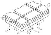
図1に、本発明の薄膜太陽電池の好ましい一例の一部の模式的な斜視断面図を示す。この薄膜太陽電池は、絶縁透光性基板1と、絶縁透光性基板1上に形成された透明導電膜2とを含んでいる。そして、絶縁透光性基板1上には互いに直交しており透明導電膜2を複数に分離している第1分離溝5(図1の矢印B方向に形成)と第2分離溝12(図1の矢印A方向に形成)とが形成されている。また、絶縁透光性基板1上には第1分離溝5に平行な第1開口溝7と、第2分離溝12に平行な第2開口溝8a、8bとが形成されている。ここで、第1開口溝7と第2開口溝8a、8bとは互いに直交している。 FIG. 1 shows a schematic perspective sectional view of a part of a preferable example of the thin film solar cell of the present invention. This thin-film solar cell includes an insulating
また、第1開口溝7を挟んで隣接する位置には太陽電池セル10と太陽電池セル11とが設置されている。さらに、第2開口溝8aを挟んで隣接する位置には太陽電池セル10と太陽電池セル13とが設置されており、第2開口溝8bを挟んで隣接する位置には太陽電池セル13と太陽電池セル14とが設置されている。ここで、太陽電池セル10、11、13、14はそれぞれ絶縁透光性基板1上に形成された光電変換層3と裏面電極4とから形成されている。 In addition,
第1開口溝7を挟んで隣接している一対の太陽電池セル10、11においては、太陽電池セル10の光電変換層3と太陽電池セル11の裏面電極4とがそれぞれ透明導電膜2と接触することによって電気的に接続されている。ここで、太陽電池セル11の裏面電極4は接続用溝6を通して透明導電膜2と接触している。 In a pair of
また、第2開口溝8aを挟んで隣接している一対の太陽電池セル10、13においては、太陽電池セル10の光電変換層3に接触している透明導電膜2と太陽電池セル13の光電変換層3に接触している透明導電膜2とが第2分離溝12により分離されており電気的に絶縁されている。また、第2開口溝8bを挟んで隣接している一対の太陽電池セル13、14においては、太陽電池セル13の光電変換層3に接触している透明導電膜2と太陽電池セル14の光電変換層3に接触している透明導電膜2とが第2分離溝により分離されておらず電気的に接続されている。したがって、この薄膜太陽電池においては、第2開口溝を挟んで隣接している一対の太陽電池セルについて、透明導電膜が第2分離溝により分離されておらず電気的に接続されているものと、透明導電膜が第2分離溝により分離されており電気的に絶縁されているものとが混在していることになる。 Further, in the pair of
従来の特許文献2に記載の薄膜太陽電池においては、第2開口溝を挟んで隣接している一対の太陽電池セルの間の透明導電膜が第2分離溝によりすべて分離されて電気的に絶縁されている。しかしながら、本発明者は、第2開口溝を挟んで隣接している一対の太陽電池セルの間の透明導電膜の一部のみを分離することによって光電変換層に短絡が生じた場合の変換効率の低下が特許文献2に記載の薄膜太陽電池と同等程度であることを見い出し、本発明を完成した。これにより、歩留りの低下の大きな要因となっていた分離溝の形成本数を特許文献2に記載の場合と比べて減少させることができるため、本発明の薄膜太陽電池は特許文献2の薄膜太陽電池と比べて歩留りが高くなる。 In the conventional thin film solar cell described in
なお、図1に示す本発明の薄膜太陽電池においては、第1分離溝5と第1開口溝7とはその設置位置が重複していないが、第2分離溝12と第2開口溝8aとは第2分離溝12の内部に第2開口溝8aが形成されているためその設置位置が重複している。また、第2分離溝12の幅Dは、第2開口溝8aの幅dよりも広くなっている。また、第1分離溝5および第2分離溝12はそれぞれ透明導電膜2の断面をその側壁としており、第1開口溝7および第2開口溝8a、8bはそれぞれ光電変換層3と裏面電極4の断面をその側壁としている。 In the thin film solar cell of the present invention shown in FIG. 1, the
ここで、絶縁透光性基板1は絶縁性と透光性とを兼ね備えた基板であって、絶縁透光性基板1としてはたとえばガラス基板を用いることができる。また、透明導電膜2としては、たとえばSnO2(酸化スズ)、ITO(Indium Tin Oxide)またはZnO(酸化亜鉛)などを用いることができる。Here, the insulating light-transmitting
また、光電変換層3としては、たとえばアモルファスシリコン薄膜からなるp層、i層およびn層が順次積層された構造、微結晶シリコン薄膜からなるp層、i層およびn層が順次積層された構造、またはアモルファスシリコン薄膜からなるp層、i層およびn層が順次積層された構造と微結晶シリコン薄膜からなるp層、i層およびn層が順次積層された構造とを組み合わせたタンデム構造などを用いることができる。 As the
また、裏面電極4としては、たとえば銀若しくはアルミニウムなどの金属薄膜またはZnOなどの透明導電膜を公知のスパッタリング法などによって形成したものなどを用いることができる。 As the
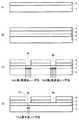
図4(a)〜(d)の模式的側面図に、図1に示す薄膜太陽電池の製造工程の一例を示す。図4(a)〜(d)は図1の矢印A方向から見た模式的な側面図である。まず、図4(a)に示すように、絶縁透光性基板1上に透明導電膜2を形成する。ここで、透明導電膜2の形成方法は特に限定されず、たとえば公知のスパッタリング法などを用いることができる。次に、図4(b)に示すように、YAG基本波レーザ光(波長;1064nm)を絶縁透光性基板1側から照射することによって、透明導電膜2の一部をレーザスクライブによって短冊状に除去して透明導電膜2を分離して第2分離溝12を形成する。ここで、図1の矢印B方向についてもYAG基本波レーザ光を用いたレーザスクライブによって透明導電膜2の一部を短冊状に除去して透明導電膜2を分離する図1に示す第1分離溝5を形成する。 An example of a manufacturing process of the thin film solar cell shown in FIG. 1 is shown in the schematic side views of FIGS. 4A to 4D are schematic side views seen from the direction of arrow A in FIG. First, as shown in FIG. 4A, a transparent
次いで、図4(c)に示すように、透明導電膜2上、第1分離溝5上および第2分離溝12上に光電変換層3と裏面電極4とを順次形成する。ここで、図1の矢印B方向については、光電変換層3の形成後で裏面電極4の形成前に光電変換層3の一部がYAG第2高調波レーザ光(波長;532nm)を用いたレーザスクライブによって短冊状に除去されて図1に示す接続用溝6が形成される。また、光電変換層3の形成方法および裏面電極4の形成方法は特に限定されず、光電変換層3の形成方法としてはたとえば高周波グロー放電プラズマCVD法などの公知のプラズマCVD法などを用いることができ、裏面電極4の形成方法としてはたとえばDCマグネトロンスパッタリング法などの公知のスパッタリング法などを用いることができる。 Next, as shown in FIG. 4C, the
そして、図4(d)に示すように、YAG第2高調波レーザ光を絶縁透光性基板1側から照射することによって、光電変換層3および裏面電極4の一部をレーザスクライブにより短冊状に除去して透明導電膜2の表面を露出させて光電変換層3および裏面電極4をそれぞれ分離する。これにより、第2開口溝8a、8bが形成される。最後に、これらの第2開口溝8a、8bに直交するようにYAG第2高調波レーザ光を絶縁透光性基板1側から照射することによって、光電変換層3および裏面電極4の一部をさらに短冊状に除去して光電変換層3および裏面電極4をそれぞれ分離する。これにより、図1に示す第2開口溝8a、8bに直交する第1開口溝7が形成されて、図1に示す薄膜太陽電池が製造される。 And as shown in FIG.4 (d), a YAG 2nd harmonic laser beam is irradiated from the insulated translucent board |
このように、本発明においては、特許文献2に記載の方法のように、YAG基本波レーザ光だけで第1分離溝、第2分離溝、第1開口溝および第2開口溝を形成することがないので、透明導電膜の昇華により発生した残滓が光電変換層または裏面電極の断面に付着する確率が減少し、透明導電膜と光電変換層との間および光電変換層と裏面電極との間における絶縁不良の発生率を減少させることができる。 As described above, in the present invention, the first separation groove, the second separation groove, the first opening groove, and the second opening groove are formed only by the YAG fundamental wave laser beam as in the method described in
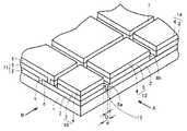
図2に、本発明の薄膜太陽電池の好ましい他の一例の一部の模式的な斜視断面図を示す。この薄膜太陽電池は、第2分離溝12の幅Dが、第2開口溝8aの幅dよりも狭くなっている点に特徴がある。ここで、第2分離溝12上に第2開口溝8aが形成されているため、第2開口溝8aと第2分離溝12とはその設置位置が重複している。 FIG. 2 shows a schematic perspective sectional view of a part of another preferred example of the thin film solar cell of the present invention. This thin-film solar cell is characterized in that the width D of the
図5(a)〜(d)の模式的側面図に、この薄膜太陽電池の製造工程の一例を示す。この図5(a)〜(d)は図2の矢印A方向から見た模式的な側面図である。まず、図5(a)に示すように、絶縁透光性基板1上に透明導電膜2を形成する。次に、図5(b)に示すように、透明導電膜2上に光電変換層3と裏面電極4とを順次形成する。ここで、図2の矢印B方向については、透明導電膜2の形成後で光電変換層3の形成前に透明導電膜2の一部がYAG基本波レーザ光を用いたレーザスクライブにより短冊状に除去されて透明導電膜2を分離する図1に示す第1分離溝5が形成され、さらに光電変換層3の形成後で裏面電極4の形成前には光電変換層3の一部がYAG第2高調波レーザ光を用いたレーザスクライブによって短冊状に除去されて接続用溝6が形成される。 An example of the manufacturing process of this thin film solar cell is shown in the schematic side view of FIGS. FIGS. 5A to 5D are schematic side views as seen from the direction of arrow A in FIG. First, as shown in FIG. 5A, a transparent
次いで、図5(c)に示すように、YAG第2高調波レーザ光を絶縁透光性基板1側から照射することによって、光電変換層3および裏面電極4の一部をレーザスクライブにより短冊状に除去して透明導電膜2の表面を露出させて光電変換層3および裏面電極4をそれぞれ分離する。これにより、第2開口溝8a、8bが形成される。続いて、これらの第2開口溝8a、8bに直交するようにYAG第2高調波レーザ光を絶縁透光性基板1側から照射することによって、光電変換層3および裏面電極4の一部を短冊状に除去して透明導電膜2の表面を露出させて光電変換層3および裏面電極4をそれぞれ分離する。これにより、図1に示す第2開口溝8a、8bに直交する第1開口溝7が形成される。 Next, as shown in FIG. 5C, a YAG second harmonic laser beam is irradiated from the insulating
最後に、図5(d)に示すように、YAG基本波レーザ光を絶縁透光性基板1側から照射することによって、図1の矢印A方向に露出した透明導電膜2の表面の一部をレーザスクライブによって短冊状に除去して透明導電膜2を分離して第2分離溝12を形成し、図2に示す薄膜太陽電池が製造される。 Finally, as shown in FIG. 5 (d), a part of the surface of the transparent
(実施例1)
幅560mm×長さ925mmのSnO2からなる透明導電膜付のガラス基板(旭硝子Uタイプ)を用意し、YAG基本波レーザ光をガラス基板側から照射することによって、透明導電膜の一部をレーザスクライブによりガラス基板の幅方向に短冊状に除去して透明導電膜を分離する第2分離溝を形成した。第2分離溝の幅は300μmであり、第2分離溝は150mmピッチで5本設けられた。また、第2分離溝の形成方向と直交する方向(ガラス基板の長さ方向)にもYAG基本波レーザ光を用いたレーザスクライブにより透明導電膜の一部を短冊状に除去して透明導電膜を分離する第1分離溝を形成した。第1分離溝の幅は100μmであり、第1分離溝は150mmピッチで3本設けられた。(Example 1)
Prepare a glass substrate (Asahi Glass U type) with SnO2 with a width of 560 mm and a length of 925 mm, and irradiate YAG fundamental wave laser light from the glass substrate side to laser a part of the transparent conductive film. A second separation groove for separating the transparent conductive film was formed by stripping in the width direction of the glass substrate by scribing. The width of the second separation groove was 300 μm, and five second separation grooves were provided at a pitch of 150 mm. Further, a transparent conductive film is also obtained by removing a part of the transparent conductive film in a strip shape by laser scribing using YAG fundamental wave laser light in a direction orthogonal to the forming direction of the second separation groove (length direction of the glass substrate). The 1st separation groove which isolate | separates was formed. The width of the first separation groove was 100 μm, and three first separation grooves were provided at a pitch of 150 mm.
次いで、透明導電膜上、第1分離溝上および第2分離溝上に光電変換層を形成した。光電変換層はアモルファスシリコン薄膜からなるp層、i層およびn層と微結晶シリコン薄膜からなるp層、i層およびn層とをガラス基板側から順次積層したタンデム構造とした。ここで、アモルファスシリコン薄膜からなるp層、i層およびn層並びに微結晶シリコン薄膜からなるp層、i層およびn層はそれぞれモノシラン(SiH4)を原料ガスとした高周波グロー放電プラズマCVD法により形成した。また、アモルファスシリコン薄膜からなるi層の厚みは0.3μmであって、微結晶シリコン薄膜からなるi層の厚みは2μmであった。そして、この光電変換層の形成後に、YAG基本波レーザ光を用いたレーザスクライブにより光電変換層の一部を除去してガラス基板の長さ方向に接続用溝を形成した。Next, a photoelectric conversion layer was formed on the transparent conductive film, the first separation groove, and the second separation groove. The photoelectric conversion layer has a tandem structure in which a p-layer made of an amorphous silicon thin film, an i-layer and an n-layer, and a p-layer made of a microcrystalline silicon thin film, an i-layer and an n-layer are sequentially laminated from the glass substrate side. Here, the p-layer, i-layer and n-layer made of an amorphous silicon thin film, and the p-layer, i-layer and n-layer made of a microcrystalline silicon thin film are each formed by high-frequency glow discharge plasma CVD using monosilane (SiH4 ) as a source gas. Formed. The thickness of the i layer made of the amorphous silicon thin film was 0.3 μm, and the thickness of the i layer made of the microcrystalline silicon thin film was 2 μm. Then, after this photoelectric conversion layer was formed, a part of the photoelectric conversion layer was removed by laser scribing using YAG fundamental wave laser light to form a connection groove in the length direction of the glass substrate.
続いて、光電変換層上に、DCマグネトロンスパッタリング法により、酸化亜鉛層と銀薄膜とを積層して裏面電極を形成した。 Subsequently, a back electrode was formed by laminating a zinc oxide layer and a silver thin film on the photoelectric conversion layer by a DC magnetron sputtering method.
最後に、YAG第2高調波レーザ光を用いたレーザスクライブによって光電変換層および裏面電極の一部をそれぞれ複数の直交する短冊状に除去して透明導電膜の表面が露出した第1開口溝および第2開口溝を形成した。これにより、図1に示す構造と同一の構造を有する実施例1の薄膜太陽電池が製造された。ここで、ガラス基板の幅方向に伸びる第2開口溝の幅は150μmで、第2開口溝は1.5mmピッチで600本形成された。また、このガラス基板の幅方向に伸びる第2開口溝の開口率はガラス基板の表面の面積の10%になるように設定された。 Finally, a first opening groove in which the surface of the transparent conductive film is exposed by removing a part of the photoelectric conversion layer and the back electrode into a plurality of orthogonal strips by laser scribing using YAG second harmonic laser light, and A second opening groove was formed. Thereby, the thin film solar cell of Example 1 which has the same structure as the structure shown in FIG. 1 was manufactured. Here, the width of the second opening groove extending in the width direction of the glass substrate was 150 μm, and 600 second opening grooves were formed at a pitch of 1.5 mm. Further, the aperture ratio of the second opening groove extending in the width direction of the glass substrate was set to be 10% of the surface area of the glass substrate.
この実施例1の薄膜太陽電池の初期効率(薄膜太陽電池の製造直後の変換効率)は、光電変換層の形成前に透明導電膜の一部をレーザスクライブにより除去してガラス基板の幅方向に5本の第2分離溝を形成しなかったこと以外は実施例1と同様にして作製した太陽電池の初期効率と比べて1.13倍となっていた。これは、特許文献2の記載の薄膜太陽電池の初期効率と同等程度であった。 The initial efficiency of the thin-film solar cell of Example 1 (conversion efficiency immediately after the production of the thin-film solar cell) is obtained by removing part of the transparent conductive film by laser scribing before forming the photoelectric conversion layer in the width direction of the glass substrate. The initial efficiency was 1.13 times that of the solar cell produced in the same manner as in Example 1 except that the five second separation grooves were not formed. This was comparable to the initial efficiency of the thin film solar cell described in
なお、実施例1において、YAG基本波レーザ光の照射条件は、ビーム径100μm、出力7W、パルス周波数5kHzおよび掃引速度200mm/秒であった。なお、分離幅300μmにおける透明導電膜の分離はYAG基本波レーザ光を4回掃引することによって形成された。また、YAG第2高調波レーザ光の照射条件は、ビーム径150μm、出力0.8W、パルス周波数9kHzおよび掃引速度500mm/秒であった。 In Example 1, the irradiation conditions of the YAG fundamental wave laser beam were a beam diameter of 100 μm, an output of 7 W, a pulse frequency of 5 kHz, and a sweep speed of 200 mm / second. The separation of the transparent conductive film with a separation width of 300 μm was formed by sweeping the YAG fundamental wave laser light four times. The irradiation conditions of the YAG second harmonic laser beam were a beam diameter of 150 μm, an output of 0.8 W, a pulse frequency of 9 kHz, and a sweep speed of 500 mm / second.
(実施例2)
幅560mm×長さ925mmのSnO2からなる透明導電膜付のガラス基板(旭硝子Uタイプ)を用意し、YAG基本波レーザ光をガラス基板側から照射することによって、透明導電膜の一部をレーザスクライブによりガラス基板の長さ方向に短冊状に除去して透明導電膜を分離する第1分離溝を形成した。この第1分離溝の幅は80μmであり、第1分離溝は150mmピッチで4本設けられた。(Example 2)
Prepare a glass substrate (Asahi Glass U type) with SnO2 with a width of 560 mm and a length of 925 mm, and irradiate YAG fundamental wave laser light from the glass substrate side to laser a part of the transparent conductive film. A first separation groove for separating the transparent conductive film was formed by stripping in the length direction of the glass substrate by scribing. The width of the first separation groove was 80 μm, and four first separation grooves were provided at a pitch of 150 mm.
次に、透明導電膜上および第1分離溝上に光電変換層を形成した。光電変換層はアモルファスシリコン薄膜からなるp層、i層およびn層と微結晶シリコン薄膜からなるp層、i層およびn層とをガラス基板側から順次積層したタンデム構造とした。ここで、アモルファスシリコン薄膜からなるp層、i層およびn層並びに微結晶シリコン薄膜からなるp層、i層およびn層はそれぞれモノシラン(SiH4)を原料ガスとした高周波グロー放電プラズマCVD法により形成した。また、アモルファスシリコン薄膜からなるi層の厚みは0.3μmであって、微結晶シリコン薄膜からなるi層の厚みは2μmであった。そして、光電変換層の形成後に、YAG基本波レーザ光を用いたレーザスクライブにより光電変換層の一部を除去してガラス基板の長さ方向に伸びる接続用溝を形成した。Next, a photoelectric conversion layer was formed on the transparent conductive film and the first separation groove. The photoelectric conversion layer has a tandem structure in which a p-layer made of an amorphous silicon thin film, an i-layer and an n-layer, and a p-layer made of a microcrystalline silicon thin film, an i-layer and an n-layer are sequentially laminated from the glass substrate side. Here, the p-layer, i-layer and n-layer made of an amorphous silicon thin film, and the p-layer, i-layer and n-layer made of a microcrystalline silicon thin film are each formed by high-frequency glow discharge plasma CVD using monosilane (SiH4 ) as a source gas. Formed. The thickness of the i layer made of the amorphous silicon thin film was 0.3 μm, and the thickness of the i layer made of the microcrystalline silicon thin film was 2 μm. Then, after the photoelectric conversion layer was formed, a part of the photoelectric conversion layer was removed by laser scribing using YAG fundamental wave laser light to form a connection groove extending in the length direction of the glass substrate.
続いて、光電変換層上に、DCマグネトロンスパッタリング法により、酸化亜鉛層と銀薄膜とを積層して裏面電極を形成した。 Subsequently, a back electrode was formed by laminating a zinc oxide layer and a silver thin film on the photoelectric conversion layer by a DC magnetron sputtering method.
次いで、YAG第2高調波レーザ光を用いたレーザスクライブによって光電変換層および裏面電極の一部をそれぞれ複数の直交する短冊状に除去して透明導電膜の表面を露出させて第1開口溝および第2開口溝を形成した。ここで、第2開口溝はガラス基板の幅方向に形成され、幅150μmで、1.5mmピッチで600本形成された。また、第2開口溝の開口率はガラス基板の表面の面積の10%になるように設定された。さらに、これらの600本の第2開口溝のうち150mm間隔の5本の第2開口溝についてYAG基本波レーザ光をガラス基板側から照射して透明導電膜の一部を除去して幅80μmの第2分離溝を形成した。 Next, the photoelectric conversion layer and a part of the back electrode are each removed into a plurality of orthogonal strips by laser scribing using a YAG second harmonic laser beam to expose the surface of the transparent conductive film, and the first opening groove and A second opening groove was formed. Here, the 2nd opening groove | channel was formed in the width direction of the glass substrate, 600 width | variety was formed with the width of 150 micrometers and 1.5 mm pitch. Further, the aperture ratio of the second opening groove was set to be 10% of the surface area of the glass substrate. Further, among these 600 second opening grooves, five second opening grooves with an interval of 150 mm are irradiated with YAG fundamental wave laser light from the glass substrate side to remove a part of the transparent conductive film to have a width of 80 μm. A second separation groove was formed.
最後に、YAG第2高調波レーザ光を用いたレーザスクライブによって光電変換層および裏面電極の一部をそれぞれ短冊状に除去して透明導電膜の表面の一部を露出させガラス基板の長さ方向に伸びる第1開口溝を形成した。これにより、図2に示す構造と同一の構造の実施例2の薄膜太陽電池が製造された。 Finally, the photoelectric conversion layer and a part of the back electrode are removed in a strip shape by laser scribing using the YAG second harmonic laser beam to expose a part of the surface of the transparent conductive film in the length direction of the glass substrate. A first opening groove extending in the direction was formed. Thereby, the thin film solar cell of Example 2 having the same structure as that shown in FIG. 2 was manufactured.
この実施例2の薄膜太陽電池の初期効率(薄膜太陽電池の製造直後の変換効率)は、第2分離溝を形成しなかったこと以外は実施例2と同様にして作製した太陽電池の初期効率と比べて1.11倍となっていた。これは、特許文献2の記載の薄膜太陽電池の初期効率と同等程度であった。 The initial efficiency of the thin-film solar cell of Example 2 (conversion efficiency immediately after the manufacture of the thin-film solar cell) is the same as that of Example 2 except that the second separation groove was not formed. Compared to 1.11 times. This was comparable to the initial efficiency of the thin film solar cell described in
なお、実施例2において、YAG基本波レーザ光の照射条件は、ビーム径80μm、出力7W、パルス周波数5kHzおよび掃引速度200mm/秒であった。また、YAG第2高調波レーザ光の照射条件は、ビーム径150μm、出力0.8W、パルス周波数9kHzおよび掃引速度500mm/秒であった。 In Example 2, the irradiation conditions of the YAG fundamental wave laser beam were a beam diameter of 80 μm, an output of 7 W, a pulse frequency of 5 kHz, and a sweep speed of 200 mm / second. The irradiation conditions of the YAG second harmonic laser beam were a beam diameter of 150 μm, an output of 0.8 W, a pulse frequency of 9 kHz, and a sweep speed of 500 mm / second.
今回開示された実施の形態および実施例はすべての点で例示であって制限的なものではないと考えられるべきである。本発明の範囲は上記した説明ではなくて特許請求の範囲によって示され、特許請求の範囲と均等の意味および範囲内でのすべての変更が含まれることが意図される。 It should be understood that the embodiments and examples disclosed herein are illustrative and non-restrictive in every respect. The scope of the present invention is defined by the terms of the claims, rather than the description above, and is intended to include any modifications within the scope and meaning equivalent to the terms of the claims.
本発明によれば、絶縁透光性基板上に設置された透明導電膜と、絶縁透光性基板上において互いに直交し透明導電膜を複数に分離している、第1分離溝と、第2分離溝と、絶縁透光性基板上において互いに直交している、第1分離溝に平行な少なくとも1本の第1開口溝と、第2分離溝に平行な少なくとも2本の第2開口溝と、を含み、第1開口溝を挟んで隣接する位置および第2開口溝を挟んで隣接する位置のそれぞれに絶縁透光性基板上に形成された、光電変換層と、裏面電極と、を含む太陽電池セルが設置されており、第1開口溝を挟んで隣接している一対の太陽電池セルにおいては、一方の太陽電池セルの光電変換層と他方の太陽電池セルの裏面電極とがそれぞれ透明導電膜と接触することによって電気的に接続され、第2開口溝を挟んで隣接している一対の太陽電池セルにおいては、一方の太陽電池セルの光電変換層に接触している透明導電膜と他方の太陽電池セルの光電変換層に接触している透明導電膜とが第2分離溝により分離されておらず電気的に接続されているものと、一方の太陽電池セルの光電変換層に接触している透明導電膜と他方の太陽電池セルの光電変換層に接触している透明導電膜とが第2分離溝により分離されており電気的に絶縁されているものとが混在している薄膜太陽電池を提供することができるので、歩留りが高く、光電変換層に短絡が生じた場合でも変換効率の低下を抑制することができる。このような本発明の薄膜太陽電池は、絶縁透光性基板側から入射した光を第1開口溝および第2開口溝を通して透過することができるシースルー型の薄膜太陽電池に好適に利用することができる。 According to the present invention, the transparent conductive film installed on the insulating light-transmitting substrate, the first separation groove that is orthogonal to each other and separates the transparent conductive film into a plurality of portions on the insulating light-transmitting substrate, and the second A separation groove, at least one first opening groove parallel to the first separation groove, and at least two second opening grooves parallel to the second separation groove, which are orthogonal to each other on the insulating translucent substrate; And a photoelectric conversion layer formed on the insulating translucent substrate at each of a position adjacent to the first opening groove and a position adjacent to the second opening groove, and a back electrode. In the pair of solar cells adjacent to each other where the solar cells are installed and sandwiching the first opening groove, the photoelectric conversion layer of one solar cell and the back electrode of the other solar cell are transparent, respectively. The second opening groove is electrically connected by contacting the conductive film. In a pair of adjacent solar cells, a transparent conductive film in contact with the photoelectric conversion layer of one solar cell and a transparent conductive film in contact with the photoelectric conversion layer of the other solar cell It is not separated by the second separation groove and is electrically connected, the transparent conductive film in contact with the photoelectric conversion layer of one solar cell, and the photoelectric conversion layer of the other solar cell. Since the thin film solar cell in which the transparent conductive film is separated from the transparent conductive film by the second separation groove and is electrically insulated can be provided, the yield is high and the photoelectric conversion layer is short-circuited. Even when this occurs, a decrease in conversion efficiency can be suppressed. Such a thin film solar cell of the present invention can be suitably used for a see-through type thin film solar cell capable of transmitting light incident from the insulating translucent substrate side through the first opening groove and the second opening groove. it can.
1 絶縁透光性基板、2 透明導電膜、3 光電変換層、4 裏面電極、5 第1分離溝、6 接続用溝、7 第1開口溝、8,8a,8b 第2開口溝、9 導線、10,11,13,14 太陽電池セル、12 第2分離溝。 DESCRIPTION OF
Claims (10)
Translated fromJapanese前記絶縁透光性基板上において互いに直交し前記透明導電膜を複数に分離している、第1分離溝と、第2分離溝と、
前記絶縁透光性基板上において互いに直交している、前記第1分離溝に平行な少なくとも1本の第1開口溝と、前記第2分離溝に平行な少なくとも2本の第2開口溝と、を含み、
前記第1開口溝を挟んで隣接する位置および前記第2開口溝を挟んで隣接する位置のそれぞれに前記絶縁透光性基板上に形成された、光電変換層と、裏面電極と、を含む太陽電池セルが設置されており、
前記第1開口溝を挟んで隣接している一対の太陽電池セルにおいては、一方の太陽電池セルの光電変換層と他方の太陽電池セルの裏面電極とがそれぞれ透明導電膜と接触することによって電気的に接続され、
前記第2開口溝を挟んで隣接している一対の太陽電池セルにおいては、一方の太陽電池セルの光電変換層に接触している透明導電膜と他方の太陽電池セルの光電変換層に接触している透明導電膜とが前記第2分離溝により分離されておらず電気的に接続されているものと、一方の太陽電池セルの光電変換層に接触している透明導電膜と他方の太陽電池セルの光電変換層に接触している透明導電膜とが前記第2分離溝により分離されており電気的に絶縁されているものとが混在しており、
前記透明導電膜を分離している前記第2分離溝が所定の間隔で配置されていることを特徴とする、薄膜太陽電池。A transparent conductive film installed on an insulating translucent substrate;
A first separation groove, a second separation groove, which are orthogonal to each other and separate the transparent conductive film into a plurality of pieces on the insulating translucent substrate;
At least one first opening groove parallel to the first separation groove and at least two second opening grooves parallel to the second separation groove, which are orthogonal to each other on the insulating translucent substrate; Including
A solar including a photoelectric conversion layer and a back electrode formed on the insulating translucent substrate at a position adjacent to the first opening groove and a position adjacent to the second opening groove, respectively. Battery cells are installed,
In a pair of solar cells adjacent to each other with the first opening groove interposed therebetween, the photoelectric conversion layer of one solar cell and the back electrode of the other solar cell come into contact with the transparent conductive film, respectively. Connected,
In the pair of solar cells adjacent to each other across the second opening groove, the transparent conductive film in contact with the photoelectric conversion layer of one solar cell and the photoelectric conversion layer of the other solar cell are in contact. A transparent conductive film that is not separated by the second separation groove and is electrically connected, and a transparent conductive film that is in contact with the photoelectric conversion layer of one solar battery cell and the other solar battery The transparent conductive film in contact with the photoelectric conversion layer of the cell is separated by the second separation groove and is electrically insulated,
The thin film solar cell,wherein the second separation grooves separating the transparent conductive film are arranged at a predetermined interval .
Priority Applications (2)
| Application Number | Priority Date | Filing Date | Title |
|---|---|---|---|
| JP2005062816AJP4340246B2 (en) | 2005-03-07 | 2005-03-07 | Thin film solar cell and manufacturing method thereof |
| US11/367,428US7750233B2 (en) | 2005-03-07 | 2006-03-06 | Thin film solar cell and manufacturing method thereof |
Applications Claiming Priority (1)
| Application Number | Priority Date | Filing Date | Title |
|---|---|---|---|
| JP2005062816AJP4340246B2 (en) | 2005-03-07 | 2005-03-07 | Thin film solar cell and manufacturing method thereof |
Publications (2)
| Publication Number | Publication Date |
|---|---|
| JP2006245507A JP2006245507A (en) | 2006-09-14 |
| JP4340246B2true JP4340246B2 (en) | 2009-10-07 |
Family
ID=36942961
Family Applications (1)
| Application Number | Title | Priority Date | Filing Date |
|---|---|---|---|
| JP2005062816AExpired - Fee RelatedJP4340246B2 (en) | 2005-03-07 | 2005-03-07 | Thin film solar cell and manufacturing method thereof |
Country Status (2)
| Country | Link |
|---|---|
| US (1) | US7750233B2 (en) |
| JP (1) | JP4340246B2 (en) |
Families Citing this family (93)
| Publication number | Priority date | Publication date | Assignee | Title |
|---|---|---|---|---|
| US9508886B2 (en) | 2007-10-06 | 2016-11-29 | Solexel, Inc. | Method for making a crystalline silicon solar cell substrate utilizing flat top laser beam |
| US8399331B2 (en) | 2007-10-06 | 2013-03-19 | Solexel | Laser processing for high-efficiency thin crystalline silicon solar cell fabrication |
| US8129822B2 (en)* | 2006-10-09 | 2012-03-06 | Solexel, Inc. | Template for three-dimensional thin-film solar cell manufacturing and methods of use |
| US8420435B2 (en) | 2009-05-05 | 2013-04-16 | Solexel, Inc. | Ion implantation fabrication process for thin-film crystalline silicon solar cells |
| US20090107545A1 (en) | 2006-10-09 | 2009-04-30 | Soltaix, Inc. | Template for pyramidal three-dimensional thin-film solar cell manufacturing and methods of use |
| JP4703433B2 (en)* | 2006-02-27 | 2011-06-15 | 三洋電機株式会社 | Photovoltaic device |
| US8035028B2 (en)* | 2006-10-09 | 2011-10-11 | Solexel, Inc. | Pyramidal three-dimensional thin-film solar cells |
| US7999174B2 (en)* | 2006-10-09 | 2011-08-16 | Solexel, Inc. | Solar module structures and assembly methods for three-dimensional thin-film solar cells |
| US8193076B2 (en) | 2006-10-09 | 2012-06-05 | Solexel, Inc. | Method for releasing a thin semiconductor substrate from a reusable template |
| US8293558B2 (en)* | 2006-10-09 | 2012-10-23 | Solexel, Inc. | Method for releasing a thin-film substrate |
| US20100304521A1 (en)* | 2006-10-09 | 2010-12-02 | Solexel, Inc. | Shadow Mask Methods For Manufacturing Three-Dimensional Thin-Film Solar Cells |
| US20080264477A1 (en)* | 2006-10-09 | 2008-10-30 | Soltaix, Inc. | Methods for manufacturing three-dimensional thin-film solar cells |
| JP2008205063A (en)* | 2007-02-19 | 2008-09-04 | Sanyo Electric Co Ltd | Solar cell module |
| WO2009026240A1 (en)* | 2007-08-17 | 2009-02-26 | Solexel, Inc. | Methods for liquid transfer coating of three-dimensional substrates |
| JP4785827B2 (en)* | 2007-12-27 | 2011-10-05 | 三洋電機株式会社 | Solar cell module and manufacturing method thereof |
| US20090215215A1 (en)* | 2008-02-21 | 2009-08-27 | Sunlight Photonics Inc. | Method and apparatus for manufacturing multi-layered electro-optic devices |
| US20090211622A1 (en)* | 2008-02-21 | 2009-08-27 | Sunlight Photonics Inc. | Multi-layered electro-optic devices |
| US8187906B2 (en) | 2008-02-28 | 2012-05-29 | Sunlight Photonics Inc. | Method for fabricating composite substances for thin film electro-optical devices |
| US20090217967A1 (en)* | 2008-02-29 | 2009-09-03 | International Business Machines Corporation | Porous silicon quantum dot photodetector |
| JP5144747B2 (en)* | 2008-03-31 | 2013-02-13 | 株式会社アルバック | SOLAR CELL MANUFACTURING METHOD, SOLAR CELL MANUFACTURING DEVICE, AND SOLAR CELL |
| KR20090110987A (en)* | 2008-04-21 | 2009-10-26 | 삼성전자주식회사 | Optical disc drive and its control method |
| US20100144080A1 (en)* | 2008-06-02 | 2010-06-10 | Solexel, Inc. | Method and apparatus to transfer coat uneven surface |
| US9711669B2 (en)* | 2008-06-09 | 2017-07-18 | Mitsubishi Electric Corporation | Thin-film photoelectric converter |
| JP2010021361A (en)* | 2008-07-10 | 2010-01-28 | Ulvac Japan Ltd | Solar cell and method of producing the same |
| US7981778B2 (en)* | 2009-07-22 | 2011-07-19 | Applied Materials, Inc. | Directional solid phase crystallization of thin amorphous silicon for solar cell applications |
| KR20110059724A (en)* | 2008-08-26 | 2011-06-03 | 어플라이드 머티어리얼스, 인코포레이티드 | Laser material removal method and apparatus |
| WO2010023845A1 (en)* | 2008-08-29 | 2010-03-04 | 株式会社アルバック | Method for manufacturing solar cell |
| JP5376873B2 (en)* | 2008-09-03 | 2013-12-25 | シャープ株式会社 | Integrated thin film solar cell |
| JP5171490B2 (en)* | 2008-09-04 | 2013-03-27 | シャープ株式会社 | Integrated thin film solar cell |
| TWI371110B (en) | 2008-09-16 | 2012-08-21 | Nexpower Technology Corp | Translucent solar cell and manufacturing method thereof |
| US20110171757A1 (en)* | 2008-09-22 | 2011-07-14 | Ulvac, Inc. | Method of manufacturing photovoltaic cell |
| JP2010074071A (en)* | 2008-09-22 | 2010-04-02 | Sharp Corp | Integrated thin film solar cell and manufacturing method thereof |
| US8288195B2 (en)* | 2008-11-13 | 2012-10-16 | Solexel, Inc. | Method for fabricating a three-dimensional thin-film semiconductor substrate from a template |
| US20100148319A1 (en)* | 2008-11-13 | 2010-06-17 | Solexel, Inc. | Substrates for High-Efficiency Thin-Film Solar Cells Based on Crystalline Templates |
| US8110428B2 (en) | 2008-11-25 | 2012-02-07 | Sunlight Photonics Inc. | Thin-film photovoltaic devices |
| MY160251A (en)* | 2008-11-26 | 2017-02-28 | Solexel Inc | Truncated pyramid -structures for see-through solar cells |
| US8541680B2 (en)* | 2008-12-03 | 2013-09-24 | Applied Materials, Inc. | Photovoltaic cells including peaks and methods of manufacture |
| US8835748B2 (en) | 2009-01-06 | 2014-09-16 | Sunlight Photonics Inc. | Multi-junction PV module |
| US8926803B2 (en)* | 2009-01-15 | 2015-01-06 | Solexel, Inc. | Porous silicon electro-etching system and method |
| US8906218B2 (en) | 2010-05-05 | 2014-12-09 | Solexel, Inc. | Apparatus and methods for uniformly forming porous semiconductor on a substrate |
| US9076642B2 (en) | 2009-01-15 | 2015-07-07 | Solexel, Inc. | High-Throughput batch porous silicon manufacturing equipment design and processing methods |
| KR20100088016A (en)* | 2009-01-29 | 2010-08-06 | 삼성전자주식회사 | Solar cell module and method for manufacturing the same |
| MY162405A (en)* | 2009-02-06 | 2017-06-15 | Solexel Inc | Trench Formation Method For Releasing A Thin-Film Substrate From A Reusable Semiconductor Template |
| EP2403007A4 (en)* | 2009-02-27 | 2017-08-02 | Kyocera Corporation | Photoelectric conversion module and method of producing same |
| US8828517B2 (en) | 2009-03-23 | 2014-09-09 | Solexel, Inc. | Structure and method for improving solar cell efficiency and mechanical strength |
| WO2010120850A1 (en)* | 2009-04-14 | 2010-10-21 | Solexel, Inc. | High efficiency epitaxial chemical vapor deposition (cvd) reactor |
| US9099584B2 (en)* | 2009-04-24 | 2015-08-04 | Solexel, Inc. | Integrated three-dimensional and planar metallization structure for thin film solar cells |
| MY165969A (en) | 2009-05-05 | 2018-05-18 | Solexel Inc | High-productivity porous semiconductor manufacturing equipment |
| US9318644B2 (en) | 2009-05-05 | 2016-04-19 | Solexel, Inc. | Ion implantation and annealing for thin film crystalline solar cells |
| TW201041161A (en)* | 2009-05-13 | 2010-11-16 | Axuntek Solar Energy Co Ltd | Solar cell structure and manufacturing method thereof |
| DE102009022318A1 (en)* | 2009-05-22 | 2010-12-23 | Schott Solar Ag | Method for producing a photovoltaic module |
| US8445314B2 (en)* | 2009-05-22 | 2013-05-21 | Solexel, Inc. | Method of creating reusable template for detachable thin film substrate |
| JP2010272738A (en)* | 2009-05-22 | 2010-12-02 | Sanyo Electric Co Ltd | Manufacturing method of solar cell module |
| WO2010138976A1 (en)* | 2009-05-29 | 2010-12-02 | Solexel, Inc. | Three-dimensional thin-film semiconductor substrate with through-holes and methods of manufacturing |
| JP2010282998A (en)* | 2009-06-02 | 2010-12-16 | Seiko Epson Corp | Solar cell and method for manufacturing solar cell |
| WO2011000814A2 (en)* | 2009-06-29 | 2011-01-06 | Reis Gmbh & Co. Kg Maschinenfabrik | Method for exposing an electrical contact |
| KR20110018654A (en)* | 2009-08-18 | 2011-02-24 | 현대중공업 주식회사 | Trench line for disconnection of solar cells |
| JP4951699B2 (en)* | 2009-08-19 | 2012-06-13 | 三洋電機株式会社 | Solar cell module and manufacturing method thereof |
| WO2011030729A1 (en)* | 2009-09-08 | 2011-03-17 | 株式会社アルバック | Solar cell module |
| KR20110032939A (en)* | 2009-09-24 | 2011-03-30 | 삼성전자주식회사 | Solar cell and manufacturing method thereof |
| JP2013506995A (en)* | 2009-10-01 | 2013-02-28 | エルジー イノテック カンパニー リミテッド | Photovoltaic power generation apparatus and manufacturing method thereof |
| KR101295547B1 (en)* | 2009-10-07 | 2013-08-12 | 엘지전자 주식회사 | Thin film type solar cell module and manufacturing method thereof |
| JPWO2011052426A1 (en)* | 2009-10-26 | 2013-03-21 | 株式会社アルバック | Solar cell evaluation apparatus and evaluation method |
| CN102763226B (en) | 2009-12-09 | 2016-01-27 | 速力斯公司 | Use high-efficiency photovoltaic back of the body contact solar cell structure and the manufacture method of thin plate semiconductor |
| WO2011078171A1 (en)* | 2009-12-22 | 2011-06-30 | 株式会社アルバック | Method for evaluating solar cell and device for evaluating same |
| DE102009060618A1 (en)* | 2009-12-28 | 2011-06-30 | Signet Solar GmbH, 04720 | Thin-film solar cell module with series-connected solar cells |
| DE102010005970A1 (en)* | 2010-01-28 | 2011-08-18 | SCHOTT Solar AG, 55122 | Process for producing a photovoltaic thin-film module |
| US8241940B2 (en) | 2010-02-12 | 2012-08-14 | Solexel, Inc. | Double-sided reusable template for fabrication of semiconductor substrates for photovoltaic cell and microelectronics device manufacturing |
| KR20130051013A (en) | 2010-06-09 | 2013-05-16 | 솔렉셀, 인크. | High productivity thin film deposition method and system |
| US8563351B2 (en)* | 2010-06-25 | 2013-10-22 | Taiwan Semiconductor Manufacturing Co., Ltd. | Method for manufacturing photovoltaic device |
| EP2601687A4 (en) | 2010-08-05 | 2018-03-07 | Solexel, Inc. | Backplane reinforcement and interconnects for solar cells |
| JP5608030B2 (en)* | 2010-09-29 | 2014-10-15 | 昭和シェル石油株式会社 | Method for producing compound thin film solar cell module |
| US9748414B2 (en) | 2011-05-20 | 2017-08-29 | Arthur R. Zingher | Self-activated front surface bias for a solar cell |
| WO2013009857A1 (en)* | 2011-07-11 | 2013-01-17 | The University Of Toledo | Translucent solar cell |
| GB2492972B (en)* | 2011-07-15 | 2013-09-11 | M Solv Ltd | Method and apparatus for dividing a thin film device into separate cells |
| KR20130107115A (en)* | 2012-03-21 | 2013-10-01 | 삼성에스디아이 주식회사 | Solar cell and manufacturing method thereof |
| DE102012111895A1 (en)* | 2012-12-06 | 2014-06-12 | Lpkf Laser & Electronics Ag | Method for producing solar module, involves heating electrical contact layer to preset temperature by laser radiation so that partial recesses are formed by removing portion of semiconductor layer together with electrical contact layer |
| CN103258881B (en)* | 2013-05-07 | 2015-11-11 | 宁波山迪光能技术有限公司 | Thin-film solar cell panel and preparation method thereof |
| US10770608B2 (en)* | 2013-05-23 | 2020-09-08 | Garmin Switzerland Gmbh | Semi-transparent thin-film photovoltaic mono cell |
| TWI459574B (en)* | 2013-11-25 | 2014-11-01 | Nexpower Technology Corp | High transmittance thin film solar panels |
| TWI464894B (en)* | 2014-02-12 | 2014-12-11 | Nexpower Technology Corp | Thin film solar panels for the prevention and treatment of thermal damage |
| FR3026230B1 (en)* | 2014-09-19 | 2016-11-18 | Commissariat Energie Atomique | SEMI-TRANSPARENT PHOTOVOLTAIC DEVICE WITH THROUGH HOLE |
| NL2016708B1 (en)* | 2016-04-29 | 2017-11-16 | Stichting Energieonderzoek Centrum Nederland | A method for manufacturing interconnected solar cells and such interconnected solar cells. |
| FR3061606A1 (en)* | 2016-12-29 | 2018-07-06 | Sunpartner Technologies | METHOD FOR THE LASER ABLATION OF THIN LAYERS FOR THE PRODUCTION OF SEMI-TRANSPARENT PHOTOVOLTAIC MODULES |
| FR3067858A1 (en) | 2017-06-16 | 2018-12-21 | Sunpartner Technologies | TWO-STAGE THIN FILM LASER ABLATION PROCESS FOR THE PRODUCTION OF SEMI-TRANSPARENT PHOTOVOLTAIC MODULES |
| EP3435424A1 (en)* | 2017-07-27 | 2019-01-30 | Nederlandse Organisatie voor toegepast- natuurwetenschappelijk onderzoek TNO | A photovoltaic panel and method of manufacturing the same |
| KR20200092943A (en)* | 2017-09-29 | 2020-08-04 | (씨엔비엠) 벵부 디자인 앤드 리서치 인스티튜트 포 글래스 인더스트리 컴퍼니 리미티드 | Translucent thin film solar module |
| WO2019062788A1 (en)* | 2017-09-29 | 2019-04-04 | (Cnbm) Bengbu Design & Research Institute For Glass Industry Co., Ltd | Semitransparent thin-film solar module |
| EP3698410A4 (en)* | 2017-09-29 | 2021-10-06 | (CNBM) Bengbu Design & Research Institute for Glass Industry Co., Ltd. | SEMITRANSPARENT THIN-FILM SOLAR MODULE |
| EP3493274A1 (en)* | 2017-12-04 | 2019-06-05 | Bengbu Design & Research Institute for Glass Industry | Thin film solar module with improved shunt resistor |
| FR3084203A1 (en) | 2018-07-20 | 2020-01-24 | Sunpartner Technologies | INDUSTRIAL METHOD OF LASER ABLATION OF THIN FILMS IN ONE STEP FOR THE PRODUCTION OF SEMI-TRANSPARENT PHOTOVOLTAIC MODULES |
| US11495708B2 (en)* | 2019-10-31 | 2022-11-08 | Korea Institute Of Science And Technology | Method of fabricating see-through thin film solar cell |
| JP2024510506A (en)* | 2021-03-19 | 2024-03-07 | ファースト・ソーラー・インコーポレーテッド | Photovoltaic devices with conductive layer interconnects |
Family Cites Families (11)
| Publication number | Priority date | Publication date | Assignee | Title |
|---|---|---|---|---|
| JPH0660155U (en) | 1993-01-12 | 1994-08-19 | 鐘淵化学工業株式会社 | Integrated solar cell module |
| JPH11312816A (en) | 1998-04-30 | 1999-11-09 | Kanegafuchi Chem Ind Co Ltd | Integrated thin-film solar cell module |
| JP4053193B2 (en) | 1999-08-25 | 2008-02-27 | 株式会社カネカ | Thin film photoelectric conversion module |
| AU7684001A (en) | 2000-07-06 | 2002-01-21 | Bp Corp North America Inc | Partially transparent photovoltaic modules |
| JP4233741B2 (en) | 2000-09-27 | 2009-03-04 | 三菱重工業株式会社 | Solar cell module and manufacturing method thereof |
| JP2002124689A (en) | 2000-10-12 | 2002-04-26 | Sekisui Chem Co Ltd | Amorphous silicon solar cell module, solar power generation system for electric power using the same, and solar cell module integrated with building material |
| JP3720254B2 (en) | 2000-10-13 | 2005-11-24 | シャープ株式会社 | Thin film solar cell and manufacturing method thereof |
| JP2002299663A (en) | 2001-03-30 | 2002-10-11 | Kanegafuchi Chem Ind Co Ltd | See-through thin-film solar cell module |
| JP4175617B2 (en) | 2002-07-29 | 2008-11-05 | 日鐵住金建材株式会社 | Slope stabilization method and structure for rockfall prevention and connecting metal fittings used therefor |
| JP4261169B2 (en) | 2002-12-03 | 2009-04-30 | 株式会社カネカ | Translucent thin film solar cell and method for producing translucent thin film solar cell module |
| JP2004330271A (en) | 2003-05-09 | 2004-11-25 | Kanegafuchi Chem Ind Co Ltd | Manufacturing method of light transmitting thin film solar cell |
- 2005
- 2005-03-07JPJP2005062816Apatent/JP4340246B2/ennot_activeExpired - Fee Related
- 2006
- 2006-03-06USUS11/367,428patent/US7750233B2/ennot_activeExpired - Fee Related
Also Published As
| Publication number | Publication date |
|---|---|
| JP2006245507A (en) | 2006-09-14 |
| US7750233B2 (en) | 2010-07-06 |
| US20060196536A1 (en) | 2006-09-07 |
Similar Documents
| Publication | Publication Date | Title |
|---|---|---|
| JP4340246B2 (en) | Thin film solar cell and manufacturing method thereof | |
| AU2004204637B2 (en) | Transparent thin-film solar cell module and its manufacturing method | |
| JP3510740B2 (en) | Manufacturing method of integrated thin-film solar cell | |
| JP6360340B2 (en) | Manufacturing method of solar cell module | |
| JP2006332453A (en) | Thin film solar cell manufacturing method and thin film solar cell | |
| US8941160B2 (en) | Photoelectric conversion module and method of manufacturing the same | |
| JP2007317868A (en) | Chalcopyrite solar cell and method for manufacturing the same | |
| JPWO2010064549A1 (en) | Method for manufacturing thin film photoelectric conversion device | |
| TW201724538A (en) | Thin film type solar cell and manufacturing method thereof | |
| JP3655025B2 (en) | Thin film photoelectric conversion device and manufacturing method thereof | |
| JP2007324633A (en) | Integrated tandem-type thin film solar cell module and its manufacturing method | |
| CN102725855B (en) | Photoelectric conversion device and method for manufacturing the same | |
| JP2002203976A (en) | Thin film solar cell and its fabricating method | |
| TWI495136B (en) | Solar cell and method of manufacturing same | |
| JP2007073745A (en) | Integrated thin-film solar cell and method for manufacturing the same | |
| TW201316537A (en) | Method for manufacturing a transmissive solar cell module | |
| JP4127994B2 (en) | Photovoltaic device manufacturing method | |
| CA2716361A1 (en) | Insulating glass unit with integrated mini-junction device | |
| CN102074598A (en) | Solar cell module and method for manufacturing the same | |
| JP2002280580A (en) | Integrated photovoltaic device and manufacturing method therefor | |
| JP2001217435A (en) | Thin film solar cell and method of manufacturing the same | |
| JP4061317B2 (en) | Solar cell and method for manufacturing solar cell | |
| JP2808005B2 (en) | Manufacturing method of amorphous solar cell | |
| JP2013219143A (en) | Thin-film solar cell module and thin-film solar cell module manufacturing method | |
| JP2009049227A (en) | Integrated multi-junction thin film silicon solar cell module and its manufacturing method |
Legal Events
| Date | Code | Title | Description |
|---|---|---|---|
| A621 | Written request for application examination | Free format text:JAPANESE INTERMEDIATE CODE: A621 Effective date:20070302 | |
| A977 | Report on retrieval | Free format text:JAPANESE INTERMEDIATE CODE: A971007 Effective date:20081029 | |
| A131 | Notification of reasons for refusal | Free format text:JAPANESE INTERMEDIATE CODE: A131 Effective date:20081111 | |
| A521 | Request for written amendment filed | Free format text:JAPANESE INTERMEDIATE CODE: A523 Effective date:20090107 | |
| TRDD | Decision of grant or rejection written | ||
| A01 | Written decision to grant a patent or to grant a registration (utility model) | Free format text:JAPANESE INTERMEDIATE CODE: A01 Effective date:20090630 | |
| A01 | Written decision to grant a patent or to grant a registration (utility model) | Free format text:JAPANESE INTERMEDIATE CODE: A01 | |
| A61 | First payment of annual fees (during grant procedure) | Free format text:JAPANESE INTERMEDIATE CODE: A61 Effective date:20090703 | |
| R150 | Certificate of patent or registration of utility model | Free format text:JAPANESE INTERMEDIATE CODE: R150 | |
| FPAY | Renewal fee payment (event date is renewal date of database) | Free format text:PAYMENT UNTIL: 20120710 Year of fee payment:3 | |
| FPAY | Renewal fee payment (event date is renewal date of database) | Free format text:PAYMENT UNTIL: 20120710 Year of fee payment:3 | |
| FPAY | Renewal fee payment (event date is renewal date of database) | Free format text:PAYMENT UNTIL: 20130710 Year of fee payment:4 | |
| LAPS | Cancellation because of no payment of annual fees |