JP4339739B2 - Multi-layer board with built-in components - Google Patents
Multi-layer board with built-in componentsDownload PDFInfo
- Publication number
- JP4339739B2 JP4339739B2JP2004129834AJP2004129834AJP4339739B2JP 4339739 B2JP4339739 B2JP 4339739B2JP 2004129834 AJP2004129834 AJP 2004129834AJP 2004129834 AJP2004129834 AJP 2004129834AJP 4339739 B2JP4339739 B2JP 4339739B2
- Authority
- JP
- Japan
- Prior art keywords
- component
- metal
- layer
- hole
- metal core
- Prior art date
- Legal status (The legal status is an assumption and is not a legal conclusion. Google has not performed a legal analysis and makes no representation as to the accuracy of the status listed.)
- Expired - Fee Related
Links
Images


Classifications
- H—ELECTRICITY
- H01—ELECTRIC ELEMENTS
- H01L—SEMICONDUCTOR DEVICES NOT COVERED BY CLASS H10
- H01L23/00—Details of semiconductor or other solid state devices
- H01L23/52—Arrangements for conducting electric current within the device in operation from one component to another, i.e. interconnections, e.g. wires, lead frames
- H01L23/538—Arrangements for conducting electric current within the device in operation from one component to another, i.e. interconnections, e.g. wires, lead frames the interconnection structure between a plurality of semiconductor chips being formed on, or in, insulating substrates
- H01L23/5389—Arrangements for conducting electric current within the device in operation from one component to another, i.e. interconnections, e.g. wires, lead frames the interconnection structure between a plurality of semiconductor chips being formed on, or in, insulating substrates the chips being integrally enclosed by the interconnect and support structures
- H—ELECTRICITY
- H01—ELECTRIC ELEMENTS
- H01L—SEMICONDUCTOR DEVICES NOT COVERED BY CLASS H10
- H01L23/00—Details of semiconductor or other solid state devices
- H01L23/12—Mountings, e.g. non-detachable insulating substrates
- H01L23/14—Mountings, e.g. non-detachable insulating substrates characterised by the material or its electrical properties
- H01L23/142—Metallic substrates having insulating layers
- H—ELECTRICITY
- H01—ELECTRIC ELEMENTS
- H01L—SEMICONDUCTOR DEVICES NOT COVERED BY CLASS H10
- H01L23/00—Details of semiconductor or other solid state devices
- H01L23/52—Arrangements for conducting electric current within the device in operation from one component to another, i.e. interconnections, e.g. wires, lead frames
- H01L23/538—Arrangements for conducting electric current within the device in operation from one component to another, i.e. interconnections, e.g. wires, lead frames the interconnection structure between a plurality of semiconductor chips being formed on, or in, insulating substrates
- H01L23/5383—Multilayer substrates
- H—ELECTRICITY
- H01—ELECTRIC ELEMENTS
- H01L—SEMICONDUCTOR DEVICES NOT COVERED BY CLASS H10
- H01L24/00—Arrangements for connecting or disconnecting semiconductor or solid-state bodies; Methods or apparatus related thereto
- H01L24/01—Means for bonding being attached to, or being formed on, the surface to be connected, e.g. chip-to-package, die-attach, "first-level" interconnects; Manufacturing methods related thereto
- H01L24/18—High density interconnect [HDI] connectors; Manufacturing methods related thereto
- H01L24/19—Manufacturing methods of high density interconnect preforms
- H—ELECTRICITY
- H01—ELECTRIC ELEMENTS
- H01L—SEMICONDUCTOR DEVICES NOT COVERED BY CLASS H10
- H01L24/00—Arrangements for connecting or disconnecting semiconductor or solid-state bodies; Methods or apparatus related thereto
- H01L24/80—Methods for connecting semiconductor or other solid state bodies using means for bonding being attached to, or being formed on, the surface to be connected
- H01L24/82—Methods for connecting semiconductor or other solid state bodies using means for bonding being attached to, or being formed on, the surface to be connected by forming build-up interconnects at chip-level, e.g. for high density interconnects [HDI]
- H—ELECTRICITY
- H05—ELECTRIC TECHNIQUES NOT OTHERWISE PROVIDED FOR
- H05K—PRINTED CIRCUITS; CASINGS OR CONSTRUCTIONAL DETAILS OF ELECTRIC APPARATUS; MANUFACTURE OF ASSEMBLAGES OF ELECTRICAL COMPONENTS
- H05K1/00—Printed circuits
- H05K1/18—Printed circuits structurally associated with non-printed electric components
- H05K1/182—Printed circuits structurally associated with non-printed electric components associated with components mounted in the printed circuit board, e.g. insert mounted components [IMC]
- H05K1/185—Components encapsulated in the insulating substrate of the printed circuit or incorporated in internal layers of a multilayer circuit
- H—ELECTRICITY
- H01—ELECTRIC ELEMENTS
- H01L—SEMICONDUCTOR DEVICES NOT COVERED BY CLASS H10
- H01L2224/00—Indexing scheme for arrangements for connecting or disconnecting semiconductor or solid-state bodies and methods related thereto as covered by H01L24/00
- H01L2224/01—Means for bonding being attached to, or being formed on, the surface to be connected, e.g. chip-to-package, die-attach, "first-level" interconnects; Manufacturing methods related thereto
- H01L2224/02—Bonding areas; Manufacturing methods related thereto
- H01L2224/04—Structure, shape, material or disposition of the bonding areas prior to the connecting process
- H01L2224/04105—Bonding areas formed on an encapsulation of the semiconductor or solid-state body, e.g. bonding areas on chip-scale packages
- H—ELECTRICITY
- H01—ELECTRIC ELEMENTS
- H01L—SEMICONDUCTOR DEVICES NOT COVERED BY CLASS H10
- H01L2224/00—Indexing scheme for arrangements for connecting or disconnecting semiconductor or solid-state bodies and methods related thereto as covered by H01L24/00
- H01L2224/01—Means for bonding being attached to, or being formed on, the surface to be connected, e.g. chip-to-package, die-attach, "first-level" interconnects; Manufacturing methods related thereto
- H01L2224/10—Bump connectors; Manufacturing methods related thereto
- H01L2224/15—Structure, shape, material or disposition of the bump connectors after the connecting process
- H01L2224/16—Structure, shape, material or disposition of the bump connectors after the connecting process of an individual bump connector
- H01L2224/161—Disposition
- H01L2224/16151—Disposition the bump connector connecting between a semiconductor or solid-state body and an item not being a semiconductor or solid-state body, e.g. chip-to-substrate, chip-to-passive
- H01L2224/16221—Disposition the bump connector connecting between a semiconductor or solid-state body and an item not being a semiconductor or solid-state body, e.g. chip-to-substrate, chip-to-passive the body and the item being stacked
- H01L2224/16225—Disposition the bump connector connecting between a semiconductor or solid-state body and an item not being a semiconductor or solid-state body, e.g. chip-to-substrate, chip-to-passive the body and the item being stacked the item being non-metallic, e.g. insulating substrate with or without metallisation
- H—ELECTRICITY
- H01—ELECTRIC ELEMENTS
- H01L—SEMICONDUCTOR DEVICES NOT COVERED BY CLASS H10
- H01L2224/00—Indexing scheme for arrangements for connecting or disconnecting semiconductor or solid-state bodies and methods related thereto as covered by H01L24/00
- H01L2224/01—Means for bonding being attached to, or being formed on, the surface to be connected, e.g. chip-to-package, die-attach, "first-level" interconnects; Manufacturing methods related thereto
- H01L2224/26—Layer connectors, e.g. plate connectors, solder or adhesive layers; Manufacturing methods related thereto
- H01L2224/31—Structure, shape, material or disposition of the layer connectors after the connecting process
- H01L2224/32—Structure, shape, material or disposition of the layer connectors after the connecting process of an individual layer connector
- H01L2224/321—Disposition
- H01L2224/32151—Disposition the layer connector connecting between a semiconductor or solid-state body and an item not being a semiconductor or solid-state body, e.g. chip-to-substrate, chip-to-passive
- H01L2224/32221—Disposition the layer connector connecting between a semiconductor or solid-state body and an item not being a semiconductor or solid-state body, e.g. chip-to-substrate, chip-to-passive the body and the item being stacked
- H01L2224/32245—Disposition the layer connector connecting between a semiconductor or solid-state body and an item not being a semiconductor or solid-state body, e.g. chip-to-substrate, chip-to-passive the body and the item being stacked the item being metallic
- H—ELECTRICITY
- H01—ELECTRIC ELEMENTS
- H01L—SEMICONDUCTOR DEVICES NOT COVERED BY CLASS H10
- H01L2224/00—Indexing scheme for arrangements for connecting or disconnecting semiconductor or solid-state bodies and methods related thereto as covered by H01L24/00
- H01L2224/73—Means for bonding being of different types provided for in two or more of groups H01L2224/10, H01L2224/18, H01L2224/26, H01L2224/34, H01L2224/42, H01L2224/50, H01L2224/63, H01L2224/71
- H01L2224/732—Location after the connecting process
- H01L2224/73251—Location after the connecting process on different surfaces
- H01L2224/73267—Layer and HDI connectors
- H—ELECTRICITY
- H01—ELECTRIC ELEMENTS
- H01L—SEMICONDUCTOR DEVICES NOT COVERED BY CLASS H10
- H01L2224/00—Indexing scheme for arrangements for connecting or disconnecting semiconductor or solid-state bodies and methods related thereto as covered by H01L24/00
- H01L2224/80—Methods for connecting semiconductor or other solid state bodies using means for bonding being attached to, or being formed on, the surface to be connected
- H01L2224/82—Methods for connecting semiconductor or other solid state bodies using means for bonding being attached to, or being formed on, the surface to be connected by forming build-up interconnects at chip-level, e.g. for high density interconnects [HDI]
- H01L2224/82009—Pre-treatment of the connector or the bonding area
- H01L2224/8203—Reshaping, e.g. forming vias
- H01L2224/82035—Reshaping, e.g. forming vias by heating means
- H01L2224/82039—Reshaping, e.g. forming vias by heating means using a laser
- H—ELECTRICITY
- H01—ELECTRIC ELEMENTS
- H01L—SEMICONDUCTOR DEVICES NOT COVERED BY CLASS H10
- H01L2224/00—Indexing scheme for arrangements for connecting or disconnecting semiconductor or solid-state bodies and methods related thereto as covered by H01L24/00
- H01L2224/80—Methods for connecting semiconductor or other solid state bodies using means for bonding being attached to, or being formed on, the surface to be connected
- H01L2224/82—Methods for connecting semiconductor or other solid state bodies using means for bonding being attached to, or being formed on, the surface to be connected by forming build-up interconnects at chip-level, e.g. for high density interconnects [HDI]
- H01L2224/82009—Pre-treatment of the connector or the bonding area
- H01L2224/8203—Reshaping, e.g. forming vias
- H01L2224/82047—Reshaping, e.g. forming vias by mechanical means, e.g. severing, pressing, stamping
- H—ELECTRICITY
- H01—ELECTRIC ELEMENTS
- H01L—SEMICONDUCTOR DEVICES NOT COVERED BY CLASS H10
- H01L2924/00—Indexing scheme for arrangements or methods for connecting or disconnecting semiconductor or solid-state bodies as covered by H01L24/00
- H01L2924/01—Chemical elements
- H01L2924/01005—Boron [B]
- H—ELECTRICITY
- H01—ELECTRIC ELEMENTS
- H01L—SEMICONDUCTOR DEVICES NOT COVERED BY CLASS H10
- H01L2924/00—Indexing scheme for arrangements or methods for connecting or disconnecting semiconductor or solid-state bodies as covered by H01L24/00
- H01L2924/01—Chemical elements
- H01L2924/01006—Carbon [C]
- H—ELECTRICITY
- H01—ELECTRIC ELEMENTS
- H01L—SEMICONDUCTOR DEVICES NOT COVERED BY CLASS H10
- H01L2924/00—Indexing scheme for arrangements or methods for connecting or disconnecting semiconductor or solid-state bodies as covered by H01L24/00
- H01L2924/01—Chemical elements
- H01L2924/01029—Copper [Cu]
- H—ELECTRICITY
- H01—ELECTRIC ELEMENTS
- H01L—SEMICONDUCTOR DEVICES NOT COVERED BY CLASS H10
- H01L2924/00—Indexing scheme for arrangements or methods for connecting or disconnecting semiconductor or solid-state bodies as covered by H01L24/00
- H01L2924/01—Chemical elements
- H01L2924/01033—Arsenic [As]
- H—ELECTRICITY
- H01—ELECTRIC ELEMENTS
- H01L—SEMICONDUCTOR DEVICES NOT COVERED BY CLASS H10
- H01L2924/00—Indexing scheme for arrangements or methods for connecting or disconnecting semiconductor or solid-state bodies as covered by H01L24/00
- H01L2924/01—Chemical elements
- H01L2924/01047—Silver [Ag]
- H—ELECTRICITY
- H01—ELECTRIC ELEMENTS
- H01L—SEMICONDUCTOR DEVICES NOT COVERED BY CLASS H10
- H01L2924/00—Indexing scheme for arrangements or methods for connecting or disconnecting semiconductor or solid-state bodies as covered by H01L24/00
- H01L2924/01—Chemical elements
- H01L2924/01078—Platinum [Pt]
- H—ELECTRICITY
- H01—ELECTRIC ELEMENTS
- H01L—SEMICONDUCTOR DEVICES NOT COVERED BY CLASS H10
- H01L2924/00—Indexing scheme for arrangements or methods for connecting or disconnecting semiconductor or solid-state bodies as covered by H01L24/00
- H01L2924/01—Chemical elements
- H01L2924/01082—Lead [Pb]
- H—ELECTRICITY
- H01—ELECTRIC ELEMENTS
- H01L—SEMICONDUCTOR DEVICES NOT COVERED BY CLASS H10
- H01L2924/00—Indexing scheme for arrangements or methods for connecting or disconnecting semiconductor or solid-state bodies as covered by H01L24/00
- H01L2924/06—Polymers
- H01L2924/078—Adhesive characteristics other than chemical
- H01L2924/07802—Adhesive characteristics other than chemical not being an ohmic electrical conductor
- H—ELECTRICITY
- H01—ELECTRIC ELEMENTS
- H01L—SEMICONDUCTOR DEVICES NOT COVERED BY CLASS H10
- H01L2924/00—Indexing scheme for arrangements or methods for connecting or disconnecting semiconductor or solid-state bodies as covered by H01L24/00
- H01L2924/10—Details of semiconductor or other solid state devices to be connected
- H01L2924/11—Device type
- H01L2924/12—Passive devices, e.g. 2 terminal devices
- H01L2924/1204—Optical Diode
- H01L2924/12042—LASER
- H—ELECTRICITY
- H01—ELECTRIC ELEMENTS
- H01L—SEMICONDUCTOR DEVICES NOT COVERED BY CLASS H10
- H01L2924/00—Indexing scheme for arrangements or methods for connecting or disconnecting semiconductor or solid-state bodies as covered by H01L24/00
- H01L2924/10—Details of semiconductor or other solid state devices to be connected
- H01L2924/11—Device type
- H01L2924/14—Integrated circuits
- H—ELECTRICITY
- H01—ELECTRIC ELEMENTS
- H01L—SEMICONDUCTOR DEVICES NOT COVERED BY CLASS H10
- H01L2924/00—Indexing scheme for arrangements or methods for connecting or disconnecting semiconductor or solid-state bodies as covered by H01L24/00
- H01L2924/15—Details of package parts other than the semiconductor or other solid state devices to be connected
- H01L2924/151—Die mounting substrate
- H01L2924/1515—Shape
- H01L2924/15153—Shape the die mounting substrate comprising a recess for hosting the device
- H—ELECTRICITY
- H01—ELECTRIC ELEMENTS
- H01L—SEMICONDUCTOR DEVICES NOT COVERED BY CLASS H10
- H01L2924/00—Indexing scheme for arrangements or methods for connecting or disconnecting semiconductor or solid-state bodies as covered by H01L24/00
- H01L2924/19—Details of hybrid assemblies other than the semiconductor or other solid state devices to be connected
- H01L2924/1901—Structure
- H01L2924/1904—Component type
- H01L2924/19041—Component type being a capacitor
- H—ELECTRICITY
- H01—ELECTRIC ELEMENTS
- H01L—SEMICONDUCTOR DEVICES NOT COVERED BY CLASS H10
- H01L2924/00—Indexing scheme for arrangements or methods for connecting or disconnecting semiconductor or solid-state bodies as covered by H01L24/00
- H01L2924/19—Details of hybrid assemblies other than the semiconductor or other solid state devices to be connected
- H01L2924/1901—Structure
- H01L2924/1904—Component type
- H01L2924/19042—Component type being an inductor
- H—ELECTRICITY
- H01—ELECTRIC ELEMENTS
- H01L—SEMICONDUCTOR DEVICES NOT COVERED BY CLASS H10
- H01L2924/00—Indexing scheme for arrangements or methods for connecting or disconnecting semiconductor or solid-state bodies as covered by H01L24/00
- H01L2924/19—Details of hybrid assemblies other than the semiconductor or other solid state devices to be connected
- H01L2924/1901—Structure
- H01L2924/1904—Component type
- H01L2924/19043—Component type being a resistor
- H—ELECTRICITY
- H01—ELECTRIC ELEMENTS
- H01L—SEMICONDUCTOR DEVICES NOT COVERED BY CLASS H10
- H01L2924/00—Indexing scheme for arrangements or methods for connecting or disconnecting semiconductor or solid-state bodies as covered by H01L24/00
- H01L2924/19—Details of hybrid assemblies other than the semiconductor or other solid state devices to be connected
- H01L2924/191—Disposition
- H01L2924/19101—Disposition of discrete passive components
- H01L2924/19105—Disposition of discrete passive components in a side-by-side arrangement on a common die mounting substrate
- H—ELECTRICITY
- H01—ELECTRIC ELEMENTS
- H01L—SEMICONDUCTOR DEVICES NOT COVERED BY CLASS H10
- H01L2924/00—Indexing scheme for arrangements or methods for connecting or disconnecting semiconductor or solid-state bodies as covered by H01L24/00
- H01L2924/30—Technical effects
- H01L2924/301—Electrical effects
- H01L2924/3025—Electromagnetic shielding
- H—ELECTRICITY
- H01—ELECTRIC ELEMENTS
- H01L—SEMICONDUCTOR DEVICES NOT COVERED BY CLASS H10
- H01L2924/00—Indexing scheme for arrangements or methods for connecting or disconnecting semiconductor or solid-state bodies as covered by H01L24/00
- H01L2924/30—Technical effects
- H01L2924/35—Mechanical effects
- H01L2924/351—Thermal stress
- H01L2924/3511—Warping
- H—ELECTRICITY
- H05—ELECTRIC TECHNIQUES NOT OTHERWISE PROVIDED FOR
- H05K—PRINTED CIRCUITS; CASINGS OR CONSTRUCTIONAL DETAILS OF ELECTRIC APPARATUS; MANUFACTURE OF ASSEMBLAGES OF ELECTRICAL COMPONENTS
- H05K2201/00—Indexing scheme relating to printed circuits covered by H05K1/00
- H05K2201/09—Shape and layout
- H05K2201/09209—Shape and layout details of conductors
- H05K2201/0929—Conductive planes
- H05K2201/09309—Core having two or more power planes; Capacitive laminate of two power planes
- H—ELECTRICITY
- H05—ELECTRIC TECHNIQUES NOT OTHERWISE PROVIDED FOR
- H05K—PRINTED CIRCUITS; CASINGS OR CONSTRUCTIONAL DETAILS OF ELECTRIC APPARATUS; MANUFACTURE OF ASSEMBLAGES OF ELECTRICAL COMPONENTS
- H05K3/00—Apparatus or processes for manufacturing printed circuits
- H05K3/46—Manufacturing multilayer circuits
- H05K3/4611—Manufacturing multilayer circuits by laminating two or more circuit boards
- H05K3/4641—Manufacturing multilayer circuits by laminating two or more circuit boards having integrally laminated metal sheets or special power cores
- Y—GENERAL TAGGING OF NEW TECHNOLOGICAL DEVELOPMENTS; GENERAL TAGGING OF CROSS-SECTIONAL TECHNOLOGIES SPANNING OVER SEVERAL SECTIONS OF THE IPC; TECHNICAL SUBJECTS COVERED BY FORMER USPC CROSS-REFERENCE ART COLLECTIONS [XRACs] AND DIGESTS
- Y10—TECHNICAL SUBJECTS COVERED BY FORMER USPC
- Y10T—TECHNICAL SUBJECTS COVERED BY FORMER US CLASSIFICATION
- Y10T428/00—Stock material or miscellaneous articles
- Y10T428/24—Structurally defined web or sheet [e.g., overall dimension, etc.]
- Y10T428/24802—Discontinuous or differential coating, impregnation or bond [e.g., artwork, printing, retouched photograph, etc.]
- Y10T428/24917—Discontinuous or differential coating, impregnation or bond [e.g., artwork, printing, retouched photograph, etc.] including metal layer
- Y—GENERAL TAGGING OF NEW TECHNOLOGICAL DEVELOPMENTS; GENERAL TAGGING OF CROSS-SECTIONAL TECHNOLOGIES SPANNING OVER SEVERAL SECTIONS OF THE IPC; TECHNICAL SUBJECTS COVERED BY FORMER USPC CROSS-REFERENCE ART COLLECTIONS [XRACs] AND DIGESTS
- Y10—TECHNICAL SUBJECTS COVERED BY FORMER USPC
- Y10T—TECHNICAL SUBJECTS COVERED BY FORMER US CLASSIFICATION
- Y10T428/00—Stock material or miscellaneous articles
- Y10T428/31504—Composite [nonstructural laminate]
- Y10T428/31678—Of metal
- Y10T428/31681—Next to polyester, polyamide or polyimide [e.g., alkyd, glue, or nylon, etc.]
Landscapes
- Engineering & Computer Science (AREA)
- Microelectronics & Electronic Packaging (AREA)
- Computer Hardware Design (AREA)
- Power Engineering (AREA)
- Physics & Mathematics (AREA)
- Condensed Matter Physics & Semiconductors (AREA)
- General Physics & Mathematics (AREA)
- Manufacturing & Machinery (AREA)
- Production Of Multi-Layered Print Wiring Board (AREA)
Description
Translated fromJapaneseこの発明は、部品内蔵型多層基板に関し、特に、サイズの異なる部品の基板内蔵化に有効な部品内蔵型多層基板に関する。 The present invention relates to a component-embedded multilayer substrate, and more particularly to a component-embedded multilayer substrate that is effective for incorporating components of different sizes.
電子部品実装の高密度化を図るべく、配線基板内部に部品を埋め込んだ部品内蔵型の多層基板が検討されている。この種の部品内蔵型多層基板としては、例えば、特許文献1に開示された構造が知られている。この特許文献1には、同文献の第5図に記載されたように、金属製のコア部材に形成された貫通孔内に部品が内蔵された構造が開示されており、部品の保護と放熱性に優れた多層基板が期待できる。In order to increase the density of electronic component mounting, a component-embedded multilayer substrate in which components are embedded inside a wiring substrate has been studied. As this kind of component-embedded multilayer substrate, for example,that is known is disclosed in
また、この特許文献1では、部品の内蔵高さを調節するために、第3図に記載されたような高さ寸法調整部材30を使用した構造が開示されている。このように、部品の内蔵高さを調整することで、サイズの異なる部品を内蔵する場合であっても、これら部品のコンタクト位置を合わせることができるため、レーザを用いてフェイスアップ接続用のコンタクト孔を形成する際に好適である。
しかし、このような高さ調整部材を用いた手法では、本来内蔵したい部品だけでなく、この高さ調整部材を装填する工程が必要になるため、改善が望まれていた。 However, in the method using such a height adjusting member, not only a part that is originally intended to be built but also a step of loading the height adjusting member is required, and therefore an improvement has been desired.
そこで、本発明は、サイズの異なる部品の基板内蔵化に有効な手法を提供する。 Therefore, the present invention provides an effective technique for incorporating components of different sizes into a substrate.
上記目的を達成するため、本発明は、金属コアに設けた収容部に部品を配置し、該金属コアの表裏両面と該収容部とが絶縁層で封止された部品内蔵型多層基板において、前記金属コアは、樹脂層を介して貼り合わせられた第1および第2の金属板を備え、該各金属板の少なくとも一部をGND層として共用し、前記樹脂層と前記第1および第2の金属板とを除去して形成された領域に、前記金属コアの表裏を貫通するスルーホール導体が前記絶縁層を介して設けられ、前記GND層として共用される部分においては、第1および第2の金属板が前記スルーホール導体を介して相互に接続されたことを特徴とする。In order to achieve the above object, the present invention provides a component-embedded multilayer substrate in which components are arranged in a housing portion provided in a metal core, and both the front and back surfaces of the metal core and the housing portion are sealed with an insulating layer.The metal core includes first and second metal plates bonded together through a resin layer, and at least a part of each metal plate is shared as a GND layer, and the resin layer and the first and second metal plates are shared. In a portion formed by removing the metal plate, through-hole conductors penetrating the front and back of the metal core are provided via the insulating layer, and in the portion shared as the GND layer, the first and first The two metal plates are connected to each other through the through-hole conductors .
ここで、収容部は、金属コアの表裏を貫通する貫通孔や、金属コアの表裏のいずれか一方に開口した座繰りのいずれをも含み、内蔵対象となる部品のサイズに応じた形状で形成される。収容部の形成は、金属コアをエッチングすることで行うことが可能である。 Here, the accommodating portion includes a through-hole penetrating the front and back of the metal core and a countersink opened on either the front or back of the metal core, and is formed in a shape corresponding to the size of the component to be incorporated. Is done. The housing portion can be formed by etching the metal core.
収容部内に配置される部品としては、トランジスタや集積回路等の能動部品およびコンデンサ、インダクタ、フィルタ等の受動部品が適宜選択可能である。これらの内蔵部品は、金属コアに形成された収容部内に配置され、金属コアの表裏両面から絶縁層で封止される。 As components arranged in the housing portion, active components such as transistors and integrated circuits and passive components such as capacitors, inductors and filters can be appropriately selected. These built-in components are arranged in a housing portion formed in the metal core, and are sealed with an insulating layer from both the front and back surfaces of the metal core.
金属コアは、絶縁層封止の際に内蔵された部品を保護し、かつ、発熱部品の放熱や能動部品のシールドとしても好適に機能する。また、この金属コアを配線パターンや電源ライン、GNDラインとして使用することも可能である。金属コアの材料としては、エッチングによる加工性、機械的剛性、放熱性、伝導性等を考慮すると、銅を用いることが望ましい。 The metal core protects the components built in when the insulating layer is sealed, and also suitably functions as heat dissipation of the heat generating components and shielding of the active components. It is also possible to use this metal core as a wiring pattern, a power supply line, or a GND line. As a material for the metal core, it is desirable to use copper in consideration of workability by etching, mechanical rigidity, heat dissipation, conductivity, and the like.
本発明では、この金属コアを複数の金属板で構成することにより、段階的なエッチングを可能とし、部品の高さに応じた収容部の形成が可能な構造を提供している。この構造は、前述の特許文献1のような高さ寸法調整部材を設ける構造とは異なり、金属板のエッチングによる収容部の高さ調整が可能であるため、製造工程の簡易化が期待できる。また、エッチングのアスペクト比が厳しいような場合であっても、段階的なエッチングが可能であるため、1層の金属板で構成するよりも、ハイアスペクトな加工が可能になる。 In the present invention, by forming the metal core with a plurality of metal plates, a stepwise etching is possible, and a structure capable of forming an accommodating portion according to the height of the component is provided. Unlike the structure provided with the height dimension adjusting member as in the above-mentioned
金属コアを構成する複数の金属板は、樹脂層を介して貼り合わせることが望ましく、このように構成することで、該樹脂層が金属板をエッチングするときのプロテクターとして機能するため、複数の金属板を貼り合わせた状態で段階的なエッチングが可能となる。よって、樹脂層の材料としては、金属板のエッチング剤に対して、耐エッチング性を有する材料を選択することが望ましく、より望ましくは、金属板に対して高い接着性を有する材料を選択する。 It is desirable that the plurality of metal plates constituting the metal core are bonded together via a resin layer. By configuring in this way, the resin layer functions as a protector when the metal plate is etched. Stepwise etching is possible with the plates attached together. Therefore, as the material of the resin layer, it is desirable to select a material having etching resistance with respect to the etching agent for the metal plate, and more desirably, a material having high adhesion to the metal plate is selected.
また、金属コアを構成する複数の金属板は、各金属板の厚さが同じであることが望ましく、このように構成することで、金属コアの反りを低減させることが可能になる。尚、金属板を3枚貼り合わせる場合は、中心の金属板を他の2枚よりも厚く形成し、両外の金属板の厚さを同じにしても良い。 Moreover, it is desirable that the plurality of metal plates constituting the metal core have the same thickness, and by configuring in this way, it is possible to reduce the warp of the metal core. When three metal plates are bonded together, the central metal plate may be formed thicker than the other two, and the thicknesses of both outer metal plates may be the same.
また、本発明は、上記構成において、前記収容部は、前記第1の金属板を除去して形成された第1の収容部と、前記第1および第2の金属板を除去して形成された第2の収容部とを備え、前記部品は、前記第1の収容部に配置された第1の部品と、前記第2の収容部に配置された第2の部品とを備えたことを特徴とする。According to the present invention, in the configuration described above, the storage portion is formed by removing the first metal plate formed by removing the first metal plate, and the first and second metal plates. A second accommodating portion, and the component comprises a first component disposed in the first accommodating portion and a second component disposed in the second accommodating portion. Features.
第1の収容部は、低背部品の収容に適した構造を有し、金属板一枚分に相当する高さの部品を収容することが可能である。尚、複数の金属板を樹脂層を介して貼り合わせた構造を採用した場合は、この樹脂層をも除去して第1の収容部としても良い。 The first accommodating portion has a structure suitable for accommodating low-profile parts, and can accommodate a component having a height corresponding to one metal plate. In addition, when the structure which bonded together the some metal plate through the resin layer is employ | adopted, this resin layer is also removed and it is good also as a 1st accommodating part.
第2の収容部は、高背部品の収容に適した構造を有し、金属板複数枚に相当する高さの部品を収容することが可能である。尚、金属コアを3枚以上の金属板で構成する場合は、金属板2枚分を除去して第1の収容部とし、金属板3枚分を除去して第2の収容部にする等、第1の収容部よりも第2の収容部の除去枚数を増加させる構成としても良く、このような実施形態も本発明に含まれるものとする。 The second accommodating portion has a structure suitable for accommodating a high-profile component, and can accommodate components having a height corresponding to a plurality of metal plates. When the metal core is composed of three or more metal plates, two metal plates are removed to form the first housing portion, and three metal plates are removed to form the second housing portion. A configuration in which the number of removed second housing portions is larger than that of the first housing portion may be adopted, and such an embodiment is also included in the present invention.
前記第1および第2の部品の前記接続ビアに対するコンタクト面は、同一高さに配置することが望ましく、このように構成することで、接続ビアの長さを一定にすることができる。その結果、接続ビア用のコンタクトを絶縁層に形成する際、レーザの出力を一定に設定した状態での加工が可能になる。 The contact surfaces of the first and second parts with respect to the connection vias are preferably arranged at the same height, and the length of the connection vias can be made constant by configuring in this way. As a result, when the contact for the connection via is formed in the insulating layer, it is possible to perform processing with the laser output being set constant.
また、第2の金属板を下地として使用することにより、第2の金属板を放熱導体として活用することができるため、発熱性の高い部品を第1の収容部に配置すれば、発熱対策を好適に行うことができる。よって、前記第1の部品は能動部品であることが望ましく、前記第2の部品は受動部品であることが望ましい。尚、第1の部品を第2の金属板に固定するにあたっては、熱伝導性の高い接着部材を用いるか、薄い接着層を介して固着することが望ましい。In addition, since the second metal plate can be used as a heat radiating conductor by using the second metal plate as a base, it is possible to take measures against heat generation by arranging a highly heat-generating component in the first housing portion. It can be suitably performed. Thus, the first component is preferably an active component, and the second component is preferably a passive component. In fixing the first component to the second metal plate, it is desirable to use an adhesive member having high thermal conductivity or to fix the first component via a thin adhesive layer.
また、貼り合わせ用の樹脂層を除去して収容部を形成することにより、第1の収容部に配置された部品を第2の金属板により近接させることが可能になるため、部品の実装安定性や放熱性の向上が期待できる。Further, by forming the housing part by removing the resin layer for bonding, since the first component disposed in the housing portion of it is possible to close the second metal plate, component mounting stability Improvement of heat dissipation and heat dissipation can be expected.
また、貼り合わせ用の樹脂層を活用して収容部を形成することにより、当該樹脂層を利用した部品の固定が可能になるため、部品配置精度の向上や部品配置工程の簡易化が期待できる。In addition, by forming the housing portion by using the resin layer for bonding, it becomes possible to fix the component using the resin layer, so that improvement of component placement accuracy and simplification of the component placement process can be expected. .
また、金属コアを貫通するスルーホール導体を設けることで、金属コアの表裏両側に設けられた配線パターンを電気的に接続することが可能になり、配線の自由度が向上する。In addition, by providing through-hole conductors that penetrate the metal core, it is possible to electrically connect the wiring patterns provided on both the front and back sides of the metal core, and the degree of freedom of wiring is improved.
このスルーホール導体は、封止用の絶縁層を介して設けても良く、この場合には、金属コアに形成した貫通孔を絶縁層で封止し、この絶縁層にレーザ若しくはドリル加工を施して開口した貫通孔の側壁に導体層を設けることで形成できる。また、このスルーホール導体は、エッチングにより露呈した金属コア層の側壁に導体層を設けることで形成しても良い。 The through-hole conductor may be provided via a sealing insulating layer. In this case, the through hole formed in the metal core is sealed with the insulating layer, and laser or drilling is performed on the insulating layer. It can be formed by providing a conductor layer on the side wall of the through hole opened. The through-hole conductor may be formed by providing a conductor layer on the side wall of the metal core layer exposed by etching.
また、金属コア内に設けた一の領域に複数のスルーホール導体を設けることで、個々のスルーホール導体ごとに専用の領域を設ける場合に比べて、スルーホール導体の高密度配置が可能になる。ここで、一の領域内に配置する複数のスルーホール導体は、隣接したスルーホール導体間の中心距離が前記金属板1枚分の厚さの3倍未満であることが望ましい。このように、狭ピッチでスルーホール導体を配置する場合は、金属板のエッチングアスペクトとの関係で、一の領域内に複数配置することが望まれる。金属板を複数貼り合わせることで、エッチングアスペクトの制限は緩和されるが、さらに高密度化したい場合には、本手法が有効である。Also, by providing a plurality of through-hole conductors in one region provided in the metal core, it is possible to arrange the through-hole conductors at a higher density than when a dedicated region is provided for each through-hole conductor. . Here, it is desirable that the plurality of through-hole conductors arranged in one region have a center distance between adjacent through-hole conductors that is less than three times the thickness of one metal plate. As described above, when through-hole conductors are arranged at a narrow pitch, it is desirable to arrange a plurality of through-hole conductors in one region in relation to the etching aspect of the metal plate. Although the limitation of the etching aspect is eased by bonding a plurality of metal plates, this method is effective when it is desired to further increase the density.
また、部品を収容した領域にスルーホール導体を共存させることで、より高密度実装が可能になる。尚、部品とともに収容するスルーホール導体は、複数本であっても良い。Further, by allowing the through-hole conductor to coexist in the region containingthe components, higher-density mounting can be achieved. In addition, the through-hole conductor accommodated with components may be plural.
また、貼り合わせ構造によって分離された第1および第2の金属板の双方をGND層として共用することで、より安定性の高いGND構造が提供できる。このGND層を共用する構造としては、第1および第2の金属板の接続を金属コアの表裏を貫通するスルーホール導体を介して行う方法が好適である。Further, by sharing both the first and second metal plates separated by the bonding structure as the GND layer, a more stable GND structure can be provided. As a structure sharing the GND layer, a method of connecting the first and second metal plates through a through-hole conductor that penetrates the front and back of the metal core is preferable.
このスルーホール導体としては、金属コアに形成された貫通孔に絶縁層を介して形成された構造と、金属コアに形成された貫通孔の壁面にメッキ等の導電処理を施して形成された構造のいずれを取ることも可能である。また、このようなスルーホール導体に替えて、金属板を貼り合わせる樹脂層に導電性を持たせることで、金属板同士を相互に接続しても良い。これらの接続処理は、少なくともGND層として共用する部分に対して行われれば良い。 As this through-hole conductor, a structure formed through an insulating layer in a through-hole formed in the metal core, and a structure formed by conducting a conductive treatment such as plating on the wall surface of the through-hole formed in the metal core Either of these can be taken. Further, instead of such a through-hole conductor, the metal plates may be connected to each other by providing conductivity to the resin layer to which the metal plates are bonded. These connection processes should just be performed with respect to the part shared as a GND layer at least.
以上説明したように、本発明によれば、高さの異なる部品を内蔵する場合であっても、部品収容部の高さ調整が簡易に行えるため、多種多様な部品の内蔵に適した多層基板が提供できる。 As described above, according to the present invention, even when components with different heights are incorporated, the height of the component accommodating portion can be easily adjusted, so that a multilayer board suitable for incorporating a wide variety of components. Can be provided.
以下、本発明に係る多層基板を添付図面を参照して詳細に説明する。尚、本発明は、以下説明する実施形態に限らず適宜変更可能である。 Hereinafter, a multilayer substrate according to the present invention will be described in detail with reference to the accompanying drawings. The present invention is not limited to the embodiments described below, and can be modified as appropriate.
図1は、本発明の第1の実施形態に係る多層基板の構造を示す断面図である。同図に示すように、本実施形態に係る多層基板10は、銅板で形成された金属層30−1、30−2が貼り合わせ樹脂層32を介して貼り合わせられた金属コア層を備え、この金属コア層の表裏面には、絶縁部材36上に配線パターン50を備えた配線層34−1、34−2がそれぞれ形成される。 FIG. 1 is a cross-sectional view showing the structure of a multilayer substrate according to the first embodiment of the present invention. As shown in the figure, the
金属コア層には、貫通孔40−1、40−2、40−3、40−4と、座繰り42とが設けられ、貫通孔40−1の内部は、絶縁部材36で充填され、貫通孔40−2、40−3の内部には、受動部品20−1、20−2が配置され、貫通孔40−4の内部には、金属コアの表裏を貫通し、配線層34−1と34−2とを導通させるスルーホール導体54が形成され、座繰り42の内部には、能動部品22が配置される。尚、スルーホール導体54の内部は、図示しない絶縁部材を充填しても良い。 The metal core layer is provided with through holes 40-1, 40-2, 40-3, 40-4, and
尚、貫通孔40−1は、ダイサーカットによる切断領域として設けられ、複数の回路モジュールを含む集合基板として作製された配線基板から、個々の回路モジュールを分断する際に使用される。尚、図示しないが貫通孔40−4の右側にも同様なダイサーカット用の貫通孔が設けられる。 In addition, the through-hole 40-1 is provided as a cutting area by dicer cutting, and is used when dividing individual circuit modules from a wiring board manufactured as a collective board including a plurality of circuit modules. Although not shown, a similar dicer cut through hole is also provided on the right side of the through hole 40-4.
上記のような構造で金属コア内に内蔵される受動部品20−1、20−2は、絶縁性接着剤24を介して配線層34−2を構成する絶縁部材36上に固定され、能動部品22は、Agペースト等の放熱性及び導電性を持った接着剤24を介して金属層30−2上に固定される。これら内蔵部品と金属コア層との間は、絶縁部材36が充填される。また、前記能動部品の裏面にグランド電極が設けられている場合、前記接着剤を介して、当該能動部品をグランド層として機能する金属コアに接続することが可能となる。 The passive components 20-1 and 20-2 built in the metal core with the above-described structure are fixed on the insulating
金属コア層の内部に内臓された受動部品20−1、20−2および能動部品22と、配線パターン50との接続は、絶縁部材36の内部に設けられた接続ビア52により行われる。同図に示すように、各内蔵部品は、接続ビア52とのコンタクト面が同一の高さとなる位置に配置されており、この配置は次の構造により得られる。 The connection between the passive components 20-1 and 20-2 and the
即ち、高背の受動部品20−1、20−2は、金属層30−1、30−2および貼り合わせ樹脂層32を除去して形成された貫通孔40−2、40−3に配置され、低背の能動部品22は、金属層30−1と貼り合わせ樹脂層32とを除去して形成された座繰り42に配置される。これにより、受動部品と能動部品との高さの差が金属層30−2の有無によって吸収され、結果として、各内蔵部品の接続ビア52に対するコンタクト面が同一高さになる。 That is, the high-passive passive components 20-1 and 20-2 are arranged in the through holes 40-2 and 40-3 formed by removing the metal layers 30-1 and 30-2 and the bonded
金属層30−2は、接続ビア52を介して配線層34−2に設けられた配線パターン50に接続されており、この金属層30−2がGND層および放熱層として機能する。 The metal layer 30-2 is connected to the
このように、金属コア層を複数の金属層30−1、30−2を積層して構成することで、高さの異なる部品であっても接続ビアに対するコンタクト面を同一高さに設定することが可能になるとともに、背の低い側の部品は金属層30−2を放熱導体として使用できるため、本構造は、受動部品よりも背の低い能動部品を使用する場合に特に有効である。 In this way, by configuring the metal core layer by laminating the plurality of metal layers 30-1 and 30-2, the contact surface for the connection via can be set to the same height even for parts having different heights. This structure is particularly effective when an active component having a height shorter than that of a passive component is used.
図2は、本発明の第2の実施形態に係る多層基板の構造を示す断面図である。同図に示す実施形態は、金属コア層を3枚の金属層で構成した例であり、その他の構成は前述の第1の実施形態と同様である。よって、以下の説明では、本実施形態に特有の部分を重点的に説明し、第1の実施形態と同一部分についての説明および図中の符号は省略する。 FIG. 2 is a cross-sectional view showing the structure of the multilayer substrate according to the second embodiment of the present invention. The embodiment shown in the figure is an example in which the metal core layer is composed of three metal layers, and other configurations are the same as those in the first embodiment. Therefore, in the following description, the part peculiar to the present embodiment will be mainly described, and the description of the same part as the first embodiment and the reference numerals in the drawings will be omitted.
この第2の実施形態では、3枚の金属層30−1、30−2、30−3を貼り合わせ樹脂層32−1、32−2を介して貼り合わせることにより金属コア層を構成する。この金属コア層は、金属層30−1、30−2および貼り合わせ樹脂層32−1、32−2を除去して形成された座繰り42−1と、金属層30−1、30−2および貼り合わせ樹脂層32−1を除去して形成された座繰り42−2と、金属層30−1および貼り合わせ樹脂層32−1を除去して形成された座繰り42−3とを具備する。 In the second embodiment, the metal core layer is configured by bonding the three metal layers 30-1, 30-2, and 30-3 via the bonding resin layers 32-1 and 32-2. The metal core layer includes a countersink 42-1 formed by removing the metal layers 30-1 and 30-2 and the bonding resin layers 32-1 and 32-2, and the metal layers 30-1 and 30-2. And a countersink 42-2 formed by removing the bonding resin layer 32-1, and a countersink 42-3 formed by removing the metal layer 30-1 and the bonding resin layer 32-1. To do.
これら座繰り42−1、42−2、42−3には、高さの異なる3つの部品20−1、20−2、22がそれぞれ配置され、各部品の接続ビアに対するコンタクト面が同一高さに設定される。 In these countersinks 42-1, 42-2, and 42-3, three parts 20-1, 20-2, and 22 having different heights are respectively arranged, and the contact surfaces for the connection vias of each part have the same height. Set to
このように、金属層を3枚用いることで、部品高さのバリエーションを増加させることができる。もっとも、本実施形態は、全ての金属層を除去して形成された貫通孔に部品を内蔵する構造に適用することも可能である。 Thus, the use of three metal layers can increase the variation in component height. But this embodiment can also be applied to the structure which incorporates components in the through-hole formed by removing all the metal layers.
図3は、本発明の第3の実施形態に係る多層基板の構造を示す断面図である。同図に示す実施形態は、部品とスルーホール導体とを同じ貫通孔に配置した構造と、金属コア層から裏面側の配線パターンへの接続を重視した構造を示す例であり、その他の構成は前述の第1の実施形態と同様である。よって、以下の説明では、本実施形態に特有の部分を重点的に説明し、第1の実施形態と同一部分についての説明および図中の符号は省略する。 FIG. 3 is a cross-sectional view showing the structure of the multilayer substrate according to the third embodiment of the present invention. The embodiment shown in the figure is an example showing a structure in which parts and through-hole conductors are arranged in the same through hole, and a structure in which connection from the metal core layer to the wiring pattern on the back side is emphasized. This is the same as in the first embodiment. Therefore, in the following description, the part peculiar to the present embodiment will be mainly described, and the description of the same part as the first embodiment and the reference numerals in the drawings will be omitted.
この第3の実施形態では、金属コア層に形成した貫通孔40−2にスルーホール導体54−1と受動部品20とが配置され、この部品20が接続ビア52−1を介して表面側の配線パターンに接続されるとともに、接続ビア52−2を介して裏面側の配線パターンに接続される。 In the third embodiment, the through-hole conductor 54-1 and the
同様に、金属コア層も表面側の配線パターンに接続される部分には、接続ビア52−1が設けられ、裏面側の配線パターンに接続される部分には、接続ビア52−2が設けられる。その他、座繰り42に配置された能動部品22や貫通孔40−3に配置されたスルーホール導体54−2が適宜設けられる。 Similarly, a connection via 52-1 is provided in a portion where the metal core layer is connected to the wiring pattern on the front surface side, and a connection via 52-2 is provided in a portion connected to the wiring pattern on the back surface side. . In addition, an
このように、部品とスルーホール導体を同一の貫通孔内に配置することで、より高密実装が可能になり、また、裏面側のパターンを有効に活用することで、配線自由度の向上が期待できる。 In this way, by arranging the parts and through-hole conductors in the same through-hole, higher-density mounting becomes possible, and by utilizing the pattern on the back side effectively, improvement in wiring flexibility is expected. it can.
図4は、本発明の第4の実施形態に係る多層基板の構造を示す断面図である。同図に示す実施形態は、金属コア層を貫通するスルーホール導体の配置バリエーションを示す例であり、その他の構成は前述の第1の実施形態と同様である。よって、以下の説明では、本実施形態に特有の部分を重点的に説明し、第1の実施形態と同一部分についての説明および図中の符号は省略する。 FIG. 4 is a sectional view showing the structure of a multilayer substrate according to the fourth embodiment of the present invention. The embodiment shown in the figure is an example showing a variation in the arrangement of through-hole conductors that penetrate the metal core layer, and other configurations are the same as those of the first embodiment. Therefore, in the following description, the part peculiar to the present embodiment will be mainly described, and the description of the same part as the first embodiment and the reference numerals in the drawings will be omitted.
この第4の実施形態では、貫通孔40−1にスルーホール導体54−1が配置され、貫通孔40−2にスルーホール導体54−2が配置され、貫通孔40−3に受動部品20とスルーホール導体54−3、54−4が配置され、貫通孔40−4にスルーホール導体54−5、54−6が配置される。 In the fourth embodiment, a through hole conductor 54-1 is disposed in the through hole 40-1, a through hole conductor 54-2 is disposed in the through hole 40-2, and the
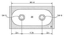
ここで、スルーホール導体54−1と54−2とは、該各スルーホール導体の中心間距離が金属層一枚の厚さtの3倍となる3t以上離れた位置に配置される。このように、スルーホール導体の間隔が3t以上離れている場合には、該各スルーホール導体の間に金属コア層を残した状態で、金属層をエッチングすることが可能であるため、各スルーホール導体を別々の貫通孔に配置し、各信号ラインの干渉防止に有効な構造を取ることができる。 Here, the through-hole conductors 54-1 and 54-2 are arranged at positions separated by 3t or more, in which the distance between the centers of the through-hole conductors is three times the thickness t of one metal layer. Thus, when the interval between the through-hole conductors is 3 t or more, the metal layer can be etched with the metal core layer remaining between the through-hole conductors. By arranging the hole conductors in separate through holes, it is possible to take a structure effective for preventing interference of each signal line.
また、スルーホール導体54−3と54−4および54−5と54−6とは、該各スルーホール導体の中心間距離が3t未満となる位置に配置される。このように、スルーホール導体の間隔が3t未満である場合には、該各スルーホール導体の間に金属コア層を残した状態で、金属層をエッチングすることが困難であるため、複数のスルーホール導体を3t未満の間隔で同一の貫通孔内に配置し、実装密度の向上を図る。このとき、同図に示すように、スルーホール導体54−3、54−4を部品20と同一の貫通孔40−3に配置することで、さらなる実装密度の向上が図られる。 Further, the through-hole conductors 54-3 and 54-4 and 54-5 and 54-6 are disposed at positions where the distance between the centers of the through-hole conductors is less than 3t. As described above, when the interval between the through-hole conductors is less than 3t, it is difficult to etch the metal layer with the metal core layer remaining between the through-hole conductors. The hole conductors are arranged in the same through hole at intervals of less than 3t to improve the mounting density. At this time, as shown in the figure, by arranging the through-hole conductors 54-3 and 54-4 in the same through-hole 40-3 as the
図5は、図4に示したスルーホール導体54−1、54−2の配置構造を示す平面図である。同図に示すように、これらのスルーホール導体は、金属層30に貫通形成された貫通孔40−1、40−2の中心に同心円状に配置される。スルーホール導体54−1、54−2の壁面と貫通孔40−1、40−2の壁面との距離は、金属層1枚分の厚さt以上が確保され、この部分には絶縁部材36が充填される。同様に、貫通孔40−1の壁面と貫通孔40−2の壁面との距離も、金属層1枚分の厚さt以上が確保される。 FIG. 5 is a plan view showing an arrangement structure of the through-hole conductors 54-1 and 54-2 shown in FIG. As shown in the figure, these through-hole conductors are arranged concentrically at the center of through-holes 40-1 and 40-2 formed through the
図6は、図4に示したスルーホール導体54−5、54−6の配置構造を示す平面図である。同図に示すように、これらのスルーホール導体は、各スルーホール導体の中心間距離が金属層1枚分の厚さt未満となる配置で、金属層30に貫通形成された貫通孔40−4の内部に配置される。尚、スルーホール導体54−5、54−6の壁面と貫通孔40−4の壁面との距離は、金属層1枚分の厚さt以上が確保され、この部分には絶縁部材36が充填される。 FIG. 6 is a plan view showing an arrangement structure of the through-hole conductors 54-5 and 54-6 shown in FIG. As shown in the figure, these through-hole conductors have through-holes 40- formed in the
図7は、図6に示したスルーホール導体54−5、54−6の変形配置例を示す平面図である。同図に示すように、これらのスルーホール導体は、図6に示した状態よりもさらに近接させて配置しても良い。この例では、各スルーホール導体の中心と金属層30の壁面との距離xが一定となる同軸構造が形成され、各スルーホール導体に流れる信号の電気特性および磁気特性の安定が図られる。 FIG. 7 is a plan view showing a modified arrangement example of the through-hole conductors 54-5 and 54-6 shown in FIG. As shown in the figure, these through-hole conductors may be arranged closer to the state shown in FIG. In this example, a coaxial structure is formed in which the distance x between the center of each through-hole conductor and the wall surface of the
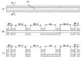
以下、図8〜図11を用いて、本発明に係る多層基板の製造方法を説明する。尚、以下の説明では、前述の第1の実施形態に係る多層基板の製造を想定し、重複する説明および図中の符号については適宜省略する。 Hereinafter, the manufacturing method of the multilayer substrate according to the present invention will be described with reference to FIGS. In the following description, it is assumed that the multilayer substrate according to the above-described first embodiment is manufactured, and overlapping descriptions and reference numerals in the drawings are omitted as appropriate.
まず、図8(a)に示すように、2枚の金属層30−1、30−2を貼り合わせ樹脂層32を介してプレス貼着し、2枚の金属層から成る金属コア層を形成する。この工程は、ラミネート加工で行っても良い。 First, as shown in FIG. 8A, the two metal layers 30-1 and 30-2 are press-bonded through the
次に、図8(b)に示すように、貼り合わせ樹脂層32を中心として、金属層30−1および30−2を両面から同時にエッチングし、貫通孔40−1〜40−5および座繰り42に対応する位置の金属層を除去する。 Next, as shown in FIG. 8 (b), the metal layers 30-1 and 30-2 are etched simultaneously from both sides around the bonded
次に、図8(c)に示すように、レーザ加工により貼り合わせ樹脂層32のうち金属層30−1および30−2から露呈した部分を除去して、貫通孔40−1〜40−5および座繰り42を形成する。 Next, as shown in FIG.8 (c), the part exposed from the metal layers 30-1 and 30-2 among the bonding resin layers 32 by laser processing is removed, and the through-holes 40-1 to 40-5 are removed. And
続いて、図9(c)に示すように、絶縁部材36から成る下地層を金属コア層の裏面に形成する。このとき、下地層として使用する絶縁部材は、流動性の低い樹脂を使用することが好ましい。 Subsequently, as shown in FIG. 9C, a base layer made of the insulating
その後、図9(d)に示すように、貫通孔40−2、40−3の底面に絶縁性接着剤24−1を塗布するとともに、座繰り42の底面に放熱性及び導電性を持った接着剤24−2を塗布し、これらの接着剤を介して受動部品20−1、20−2および能動部品22をそれぞれ配置する。 Thereafter, as shown in FIG. 9D, the insulating adhesive 24-1 was applied to the bottom surfaces of the through holes 40-2 and 40-3, and the bottom surface of the
次に、図10(e)に示すように、金属コア層の両側から樹脂層をプレスして、金属コア層の周囲および内部を絶縁部材36で封止する。このとき、金属コア層に形成された貫通孔と座繰りの内部には絶縁部材36が充填される。尚、このときプレスする樹脂層は、表面に銅箔が付された樹脂層を使用しても良く、この場合には、銅箔が付された側から樹脂層をプレスして金属コア層を絶縁部材で封止する。 Next, as shown in FIG. 10E, the resin layer is pressed from both sides of the metal core layer, and the periphery and the inside of the metal core layer are sealed with an insulating
次に、図10(f)に示すように、レーザ加工により絶縁部材36を除去して、接続ビア用コンタクト53を形成する。尚、金属コア層の封止に銅箔付きの樹脂層を使用する場合には、この銅箔をエッチングで除去した後にレーザ加工を行う。このとき、貫通孔40−4内に充填された絶縁層を開口し、スルーホール導体用の貫通孔を形成する。 Next, as shown in FIG. 10F, the insulating
その後、図11(g)に示すように、銅メッキを利用したセミアディティブ法により接続ビア用コンタクト内に接続ビア52を形成するとともに、表裏面の配線層34−1、34−2を形成する。その結果、配線層34−1、34−2上に形成された配線パターン50と、受動部品20−1、20−2および能動部品22とが接続ビア52を介して接続された状態となる。同時に貫通孔40−4内に絶縁層を介してスルーホール導体54を形成する。 Thereafter, as shown in FIG. 11G, the connection via 52 is formed in the connection via contact by the semi-additive method using copper plating, and the wiring layers 34-1 and 34-2 on the front and back surfaces are formed. . As a result, the
最後に、図11(h)に示すように、同図(g)で形成した配線層34−1、34−2の上に、さらに別の配線層34−3、34−4をそれぞれ形成する。そして、表面側の配線層34−3には、受動部品20−3、20−4と能動部品22−2を実装するとともに、裏面側の配線層34−4には外部端子を形成し、図中の1点鎖線で示したラインで分断して他のマザーボードに実装可能な回路モジュールを得る。 Finally, as shown in FIG. 11H, further wiring layers 34-3 and 34-4 are formed on the wiring layers 34-1 and 34-2 formed in FIG. . Then, the passive components 20-3 and 20-4 and the active component 22-2 are mounted on the wiring layer 34-3 on the front surface side, and external terminals are formed on the wiring layer 34-4 on the back surface side. A circuit module that can be mounted on another mother board is obtained by cutting along a line indicated by a one-dot chain line.
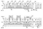
図12は、金属コア層をGNDとして使用する場合の例を示した断面図である。同図(a)に示すように、金属コア層をGNDとして使用する場合は、金属層30−1と30−2を接続ビア52、配線パターン50、スルーホール導体54を介して相互に接続し、この相互接続された領域をGND層として提供する。 FIG. 12 is a cross-sectional view illustrating an example in which the metal core layer is used as GND. As shown in FIG. 5A, when the metal core layer is used as GND, the metal layers 30-1 and 30-2 are connected to each other via the connection via 52, the
また、同図(b)に示すように、エッチングにより露呈した金属コア層の側壁に導体層を形成して得たスルーホール導体54を介して、金属層30−1と30−2を相互に接続しても良い。また、同図(a)、(b)に示したようなスルーホール導体による接続に替えて、貼り合わせ樹脂層32に導電性を持たせることで金属層30−1と30−2を相互に接続しても良い。 Further, as shown in FIG. 5B, the metal layers 30-1 and 30-2 are mutually connected through a through-
本発明によれば、部品収容部の高さ調整が簡易に行えるため、多種多様な部品の内蔵が要求される高集積回路基板への適用が期待される。 According to the present invention, since the height of the component accommodating portion can be easily adjusted, application to a highly integrated circuit board that requires the incorporation of a wide variety of components is expected.
10…多層基板、20…受動部品、22…能動部品、24…接着剤、30…金属層、32…貼り合せ樹脂層、34…配線層、36…絶縁部材、40…貫通孔、42…座繰り、50…配線パターン、52…接続ビア、53…接続ビア用コンタクト、54…スルーホール導体、56…外部端子 DESCRIPTION OF
Claims (12)
Translated fromJapanese前記金属コアは、
樹脂層を介して貼り合わせられた第1および第2の金属板を備え、該各金属板の少なくとも一部をGND層として共用し、
前記樹脂層と前記第1および第2の金属板とを除去して形成された領域に、前記金属コアの表裏を貫通するスルーホール導体が前記絶縁層を介して設けられ、
前記GND層として共用される部分においては、第1および第2の金属板が前記スルーホール導体を介して相互に接続された
ことを特徴とする部品内蔵型多層基板。In a component-embedded multilayer board in which components are arranged in a housing portion provided in a metal core, and both the front and back surfaces of the metal core and the housing portion are sealed with an insulating layer,
The metal core is
Comprising first and second metal plates bonded together via a resin layer, and at least a part of each metal plate is shared as a GND layer;
In the region formed by removing the resin layer and the first and second metal plates, through-hole conductors penetrating the front and back of the metal core are provided via the insulating layer,
A component-embedded multilayer boardin which the first and second metal plates are connected to each other through the through-hole conductor in a portion shared as the GND layer .
ことを特徴とする請求項1記載の部品内蔵型多層基板。2. The component built-in multilayer substrate according to claim 1, wherein, in a portion shared as the GND layer, the resin layer to which the first and second metal plates are bonded has conductivity .
前記第1の金属板を除去して形成された第1の収容部と、
前記第1および第2の金属板を除去して形成された第2の収容部
とを備え、
前記部品は、
前記第1の収容部に配置された第1の部品と、
前記第2の収容部に配置された第2の部品と
を備えたことを特徴とする請求項1記載の部品内蔵型多層基板。The accommodating portion is
A first accommodating portion formed by removing the first metal plate;
A second accommodating portion formed by removing the first and second metal plates
And
The parts are
A first component disposed in the first housing portion;
A second component disposed in the second housing portion;
The component built-in multilayer board accordingto claim 1, comprising:
前記第1の金属板を除去して形成された第1の収容部と、
前記第1および第2の金属板と前記樹脂層とを除去して形成された第2の収容部と
を備え、
前記部品は、
前記第1の収容部に配置された第1の部品と、
前記第2の収容部に配置された第2の部品と
を備えたことを特徴とする請求項1記載の部品内蔵型多層基板。The accommodating portion is
A first accommodating portion formed by removing the first metal plate;
A second accommodating portion formed by removing the first and second metal plates and the resin layer;
With
The parts are
A first component disposed in the first housing portion;
A second component disposed in the second housing portion;
Component built-in multilayer substrate according to claim1, furthercomprising a.
前記第1の金属板と前記樹脂層とを除去して形成された第1の収容部と、
前記第1および第2の金属板と前記樹脂層とを除去して形成された第2の収容部と
を備え、
前記部品は、
前記第1の収容部に配置された第1の部品と、
前記第2の収容部に配置された第2の部品と
を備えたことを特徴とする請求項1記載の部品内蔵型多層基板。The accommodating portion is
A first accommodating portion formed by removing the first metal plate and the resin layer;
A second accommodating portion formed by removing the first and second metal plates and the resin layer;
With
The parts are
A first component disposed in the first housing portion;
A second component disposed in the second housing portion;
The component built-in multilayer board accordingto claim 1, comprising:
前記第1および第2の部品の前記接続ビアに対するコンタクト面が同一高さに配置されたことを特徴とする請求項4乃至6のいずれかに記載の部品内蔵型多層基板。The component is formed on the insulating layer through a connection via formed in the insulating layer;
7. The component built-in multilayer substrate accordingto claim 4, wherein contact surfaces of the first and second components with respect to the connection via are arranged at the same height .
前記第2の金属板に接続された放熱用のビアを備えたことを特徴とする請求項7記載の部品内蔵型多層基板。The connection via is
8. The component built-in multilayer board accordingto claim 7, further comprising a heat dissipation via connected to the second metal plate .
Priority Applications (5)
| Application Number | Priority Date | Filing Date | Title |
|---|---|---|---|
| JP2004129834AJP4339739B2 (en) | 2004-04-26 | 2004-04-26 | Multi-layer board with built-in components |
| US11/114,781US7379306B2 (en) | 2004-04-26 | 2005-04-25 | Multilayer substrate including components therein |
| CNB2005100662826ACN100345466C (en) | 2004-04-26 | 2005-04-26 | Multilayer substrate including components therein |
| EP05252601.9AEP1592061B1 (en) | 2004-04-26 | 2005-04-26 | Multilayer substrate including components therein |
| US12/108,303US7738256B2 (en) | 2004-04-26 | 2008-04-23 | Multilayer substrate including components therein |
Applications Claiming Priority (1)
| Application Number | Priority Date | Filing Date | Title |
|---|---|---|---|
| JP2004129834AJP4339739B2 (en) | 2004-04-26 | 2004-04-26 | Multi-layer board with built-in components |
Publications (2)
| Publication Number | Publication Date |
|---|---|
| JP2005311249A JP2005311249A (en) | 2005-11-04 |
| JP4339739B2true JP4339739B2 (en) | 2009-10-07 |
Family
ID=34941041
Family Applications (1)
| Application Number | Title | Priority Date | Filing Date |
|---|---|---|---|
| JP2004129834AExpired - Fee RelatedJP4339739B2 (en) | 2004-04-26 | 2004-04-26 | Multi-layer board with built-in components |
Country Status (4)
| Country | Link |
|---|---|
| US (2) | US7379306B2 (en) |
| EP (1) | EP1592061B1 (en) |
| JP (1) | JP4339739B2 (en) |
| CN (1) | CN100345466C (en) |
Families Citing this family (66)
| Publication number | Priority date | Publication date | Assignee | Title |
|---|---|---|---|---|
| JP4339739B2 (en)* | 2004-04-26 | 2009-10-07 | 太陽誘電株式会社 | Multi-layer board with built-in components |
| US7286366B2 (en)* | 2005-03-24 | 2007-10-23 | Motorola, Inc. | Multilayer circuit board with embedded components and method of manufacture |
| KR100656751B1 (en)* | 2005-12-13 | 2006-12-13 | 삼성전기주식회사 | Electronic circuit board and manufacturing method |
| US7338892B2 (en)* | 2006-06-09 | 2008-03-04 | Advanced Semiconductor Engineering, Inc. | Circuit carrier and manufacturing process thereof |
| KR100751995B1 (en)* | 2006-06-30 | 2007-08-28 | 삼성전기주식회사 | Printed Circuit Board and Manufacturing Method |
| JP5183045B2 (en)* | 2006-07-20 | 2013-04-17 | 三洋電機株式会社 | Circuit equipment |
| WO2008056499A1 (en) | 2006-11-06 | 2008-05-15 | Nec Corporation | Semiconductor device and method for manufacturing same |
| WO2008069260A1 (en)* | 2006-11-30 | 2008-06-12 | Sanyo Electric Co., Ltd. | Circuit element mounting board, circuit device using the same, and air conditioner |
| JP5326269B2 (en)* | 2006-12-18 | 2013-10-30 | 大日本印刷株式会社 | Electronic component built-in wiring board, and heat dissipation method for electronic component built-in wiring board |
| WO2008075629A1 (en)* | 2006-12-18 | 2008-06-26 | Dai Nippon Printing Co., Ltd. | Electronic parts built-in distributing board, and radiating method for the electronic parts built-in distributing board |
| JP4976840B2 (en)* | 2006-12-22 | 2012-07-18 | 株式会社東芝 | Printed wiring board, printed wiring board manufacturing method, and electronic device |
| TWI324901B (en)* | 2007-01-08 | 2010-05-11 | Unimicron Technology Corp | Printed circuit board structure integrating electronic components |
| US8314343B2 (en) | 2007-09-05 | 2012-11-20 | Taiyo Yuden Co., Ltd. | Multi-layer board incorporating electronic component and method for producing the same |
| JP4551468B2 (en)* | 2007-09-05 | 2010-09-29 | 太陽誘電株式会社 | Electronic component built-in multilayer board |
| GB2459251A (en) | 2008-04-01 | 2009-10-21 | Sharp Kk | Semiconductor nanowire devices |
| GB2458907A (en)* | 2008-04-01 | 2009-10-07 | Sharp Kk | Device interconnects |
| US20110073357A1 (en)* | 2008-06-02 | 2011-03-31 | Nxp B.V. | Electronic device and method of manufacturing an electronic device |
| TWI363411B (en)* | 2008-07-22 | 2012-05-01 | Advanced Semiconductor Eng | Embedded chip substrate and fabrication method thereof |
| JP5432918B2 (en)* | 2008-10-31 | 2014-03-05 | 太陽誘電株式会社 | Manufacturing method of printed wiring board |
| JP5534682B2 (en)* | 2009-02-06 | 2014-07-02 | 積水化学工業株式会社 | Thermosetting adhesive for electronic components and method for manufacturing electronic component-embedded substrate using this adhesive |
| KR101018109B1 (en)* | 2009-08-24 | 2011-02-25 | 삼성전기주식회사 | Multilayer wiring board and its manufacturing method |
| KR101677284B1 (en)* | 2009-12-24 | 2016-11-18 | 삼성전자주식회사 | Embedded circuit board and manufacturing thereof |
| EP2533616A4 (en)* | 2010-02-01 | 2016-08-10 | Furukawa Electric Co Ltd | Metal core substrate for in-vehicle electrical junction box |
| WO2011102134A1 (en) | 2010-02-18 | 2011-08-25 | 株式会社村田製作所 | Component-embedded substrate |
| KR101117155B1 (en)* | 2010-07-01 | 2012-03-07 | 삼성전기주식회사 | Method for manufacturing embedded substrate |
| KR101775150B1 (en)* | 2010-07-30 | 2017-09-05 | 삼성전자주식회사 | Multi-layered laminates package and method for manufacturing the same |
| KR101167453B1 (en)* | 2010-12-23 | 2012-07-26 | 삼성전기주식회사 | A printed circuit board comprising embeded electronic component within and a method for manufacturing |
| CN102769000A (en)* | 2011-05-05 | 2012-11-07 | 国碁电子(中山)有限公司 | Embedded component packaging structure and manufacturing method |
| KR101422437B1 (en)* | 2011-05-13 | 2014-07-22 | 이비덴 가부시키가이샤 | Circuit board and manufacturing method thereof |
| JP5178899B2 (en) | 2011-05-27 | 2013-04-10 | 太陽誘電株式会社 | Multilayer board |
| KR101905879B1 (en)* | 2011-12-15 | 2018-11-28 | 엘지이노텍 주식회사 | The printed circuit board and the method for manufacturing the same |
| US9439289B2 (en)* | 2012-01-12 | 2016-09-06 | Ibiden Co., Ltd. | Wiring board and method for manufacturing the same |
| JP5236826B1 (en)* | 2012-08-15 | 2013-07-17 | 太陽誘電株式会社 | Electronic component built-in board |
| JP5261624B1 (en)* | 2012-11-05 | 2013-08-14 | 太陽誘電株式会社 | Circuit module |
| JP2014116548A (en)* | 2012-12-12 | 2014-06-26 | Ngk Spark Plug Co Ltd | Multilayer wiring board and manufacturing method therefor |
| KR102026229B1 (en)* | 2012-12-12 | 2019-09-27 | 엘지이노텍 주식회사 | Printed circuit board and manufacturing method thereof |
| JP5462404B1 (en)* | 2013-09-12 | 2014-04-02 | 太陽誘電株式会社 | Component embedded substrate and core substrate for component embedded substrate |
| SG10201400396WA (en) | 2014-03-05 | 2015-10-29 | Delta Electronics Int’L Singapore Pte Ltd | Package structure and stacked package module with the same |
| SG10201400390YA (en)* | 2014-03-05 | 2015-10-29 | Delta Electronics Int L Singapore Pte Ltd | Package structure |
| JP5750528B1 (en)* | 2014-03-26 | 2015-07-22 | 太陽誘電株式会社 | Circuit board with built-in components |
| JP2016029681A (en) | 2014-07-25 | 2016-03-03 | イビデン株式会社 | Multilayer wiring board and manufacturing method of the same |
| KR20160013706A (en)* | 2014-07-28 | 2016-02-05 | 삼성전기주식회사 | Printed circuit board and method of manufacturing the same |
| US9653438B2 (en)* | 2014-08-21 | 2017-05-16 | General Electric Company | Electrical interconnect structure for an embedded semiconductor device package and method of manufacturing thereof |
| JP6473595B2 (en)* | 2014-10-10 | 2019-02-20 | イビデン株式会社 | Multilayer wiring board and manufacturing method thereof |
| US10433424B2 (en)* | 2014-10-16 | 2019-10-01 | Cyntec Co., Ltd | Electronic module and the fabrication method thereof |
| JP2016082074A (en)* | 2014-10-17 | 2016-05-16 | ダイキン工業株式会社 | Electrical equipment and method for manufacturing the same |
| CN106356351B (en)* | 2015-07-15 | 2019-02-01 | 凤凰先驱股份有限公司 | Board structure and preparation method thereof |
| SG10201604384YA (en) | 2016-05-31 | 2017-12-28 | Delta Electronics Int'l (Singapore) Pte Ltd | Embedded package structure |
| US9887167B1 (en)* | 2016-09-19 | 2018-02-06 | Advanced Semiconductor Engineering, Inc. | Embedded component package structure and method of manufacturing the same |
| CN108307582A (en)* | 2017-01-11 | 2018-07-20 | 宁波舜宇光电信息有限公司 | The circuit board arrangement and its manufacturing method of circuit board arrangement and its manufacturing method of opening a window and embedding attachment component |
| JP6343058B2 (en)* | 2017-04-04 | 2018-06-13 | 新光電気工業株式会社 | Wiring board and method of manufacturing wiring board |
| CN107170731A (en)* | 2017-05-05 | 2017-09-15 | 华为技术有限公司 | Embedded substrate and its manufacture method |
| WO2019004266A1 (en)* | 2017-06-30 | 2019-01-03 | 株式会社村田製作所 | Electronic component module |
| JP6559743B2 (en) | 2017-08-08 | 2019-08-14 | 太陽誘電株式会社 | Semiconductor module |
| EP3481161B1 (en)* | 2017-11-02 | 2025-09-10 | AT & S Austria Technologie & Systemtechnik Aktiengesellschaft | Component carrier with transistor components arranged side by side |
| KR102026132B1 (en) | 2018-03-05 | 2019-09-27 | 삼성전자주식회사 | Fan-out semiconductor package module |
| CN111372369B (en) | 2018-12-25 | 2023-07-07 | 奥特斯科技(重庆)有限公司 | Component carrier with component shielding and method for producing the same |
| KR102415707B1 (en)* | 2019-05-15 | 2022-07-05 | 아비드 써멀 코포레이션 | Vapor Chamber Heat Strap Assemblies and Methods |
| CN112242351B (en)* | 2019-07-16 | 2024-09-20 | 中芯国际集成电路制造(上海)有限公司 | Semiconductor structure and forming method thereof |
| JP2019208045A (en)* | 2019-07-17 | 2019-12-05 | 太陽誘電株式会社 | Circuit board |
| CN112770495B (en)* | 2019-10-21 | 2022-05-27 | 宏启胜精密电子(秦皇岛)有限公司 | Omnidirectional embedded module and manufacturing method thereof, and packaging structure and manufacturing method thereof |
| WO2021081867A1 (en)* | 2019-10-31 | 2021-05-06 | 鹏鼎控股(深圳)股份有限公司 | Thin circuit board and manufacturing method therefor |
| CN111278213B (en)* | 2020-02-10 | 2021-10-01 | 广西容县菱通竞业电子有限公司 | Flexible printed circuit board |
| JP7271790B2 (en)* | 2020-04-27 | 2023-05-11 | オリンパス株式会社 | Multilayer board, probe unit, and ultrasonic endoscope |
| KR20220144107A (en)* | 2021-04-19 | 2022-10-26 | 삼성전자주식회사 | Semiconductor package and method for manufacturing the same |
| CN116261262A (en)* | 2021-12-09 | 2023-06-13 | 宏启胜精密电子(秦皇岛)有限公司 | Circuit board structure and manufacturing method thereof |
Family Cites Families (27)
| Publication number | Priority date | Publication date | Assignee | Title |
|---|---|---|---|---|
| US3663866A (en) | 1970-03-27 | 1972-05-16 | Rogers Corp | Back plane |
| JPS49131863U (en)* | 1973-03-10 | 1974-11-13 | ||
| JPS5658038A (en)* | 1979-10-12 | 1981-05-20 | Hamanaka Kk | Knitting method |
| JPS61287132A (en) | 1985-06-13 | 1986-12-17 | Matsushita Electric Works Ltd | Manufacture of chip carrier for electronic element |
| JPS61287152A (en) | 1985-06-13 | 1986-12-17 | Matsushita Electric Works Ltd | Manufacture of chip carrier for electronic element |
| FR2599893B1 (en) | 1986-05-23 | 1996-08-02 | Ricoh Kk | METHOD FOR MOUNTING AN ELECTRONIC MODULE ON A SUBSTRATE AND INTEGRATED CIRCUIT CARD |
| JPH06177544A (en) | 1992-12-03 | 1994-06-24 | Ibiden Co Ltd | Electronic component mounting board and manufacture thereof |
| US5353195A (en)* | 1993-07-09 | 1994-10-04 | General Electric Company | Integral power and ground structure for multi-chip modules |
| JPH08148782A (en) | 1994-11-15 | 1996-06-07 | Matsushita Electric Works Ltd | Metal core circuit board |
| US6020637A (en)* | 1997-05-07 | 2000-02-01 | Signetics Kp Co., Ltd. | Ball grid array semiconductor package |
| FR2780892B1 (en) | 1998-07-08 | 2001-08-17 | Sod Conseils Rech Applic | USE OF PRENYLTRANSFERASE INHIBITORS FOR THE PREPARATION OF A MEDICINAL PRODUCT FOR TREATING CONDITIONS RESULTING FROM MEMBRANE FIXATION OF HETEROTRIMERIC PROTEIN |
| GB2340058A (en)* | 1998-07-30 | 2000-02-16 | Rover Group | An apparatus for securing components upon a structural member |
| JP2000101245A (en)* | 1998-09-24 | 2000-04-07 | Ngk Spark Plug Co Ltd | Multilayer resin wiring board and its manufacture |
| SE513352C2 (en) | 1998-10-26 | 2000-08-28 | Ericsson Telefon Ab L M | Circuit board and process for making the circuit board |
| US6711812B1 (en) | 1999-04-13 | 2004-03-30 | Unicap Electronics Industrial Corporation | Method of making metal core substrate printed circuit wiring board enabling thermally enhanced ball grid array (BGA) packages |
| CN101232777B (en)* | 1999-09-02 | 2010-06-09 | 伊比登株式会社 | printed wiring board |
| EP1818975A3 (en)* | 2000-02-25 | 2010-09-29 | Ibiden Co., Ltd. | Multilayer printed circuit board and multilayer printed circuit board manufacturing method |
| JP2001244376A (en)* | 2000-02-28 | 2001-09-07 | Hitachi Ltd | Semiconductor device |
| JP2001284803A (en) | 2000-03-30 | 2001-10-12 | Nec Corp | Mounting method of printed wiring board for high frequency, printed wiring board mounting member for high frequency and its manufacturing method |
| TW511415B (en)* | 2001-01-19 | 2002-11-21 | Matsushita Electric Industrial Co Ltd | Component built-in module and its manufacturing method |
| US6855892B2 (en)* | 2001-09-27 | 2005-02-15 | Matsushita Electric Industrial Co., Ltd. | Insulation sheet, multi-layer wiring substrate and production processes thereof |
| TW550997B (en)* | 2001-10-18 | 2003-09-01 | Matsushita Electric Industrial Co Ltd | Module with built-in components and the manufacturing method thereof |
| JP2003243783A (en) | 2002-02-14 | 2003-08-29 | Ngk Spark Plug Co Ltd | Wiring board and its manufacturing method |
| JP2003332752A (en)* | 2002-05-14 | 2003-11-21 | Shinko Electric Ind Co Ltd | Metal core substrate and its manufacturing method |
| JP2003347741A (en) | 2002-05-30 | 2003-12-05 | Taiyo Yuden Co Ltd | Composite multilayer substrate and module using the same |
| JP2004128002A (en) | 2002-09-30 | 2004-04-22 | Taiyo Yuden Co Ltd | Electronic part built-in type multilayer substrate |
| JP4339739B2 (en)* | 2004-04-26 | 2009-10-07 | 太陽誘電株式会社 | Multi-layer board with built-in components |
- 2004
- 2004-04-26JPJP2004129834Apatent/JP4339739B2/ennot_activeExpired - Fee Related
- 2005
- 2005-04-25USUS11/114,781patent/US7379306B2/enactiveActive
- 2005-04-26EPEP05252601.9Apatent/EP1592061B1/ennot_activeCeased
- 2005-04-26CNCNB2005100662826Apatent/CN100345466C/ennot_activeExpired - Fee Related
- 2008
- 2008-04-23USUS12/108,303patent/US7738256B2/ennot_activeExpired - Fee Related
Also Published As
| Publication number | Publication date |
|---|---|
| EP1592061A3 (en) | 2007-07-04 |
| EP1592061B1 (en) | 2018-11-14 |
| EP1592061A2 (en) | 2005-11-02 |
| US20050255303A1 (en) | 2005-11-17 |
| US7379306B2 (en) | 2008-05-27 |
| CN100345466C (en) | 2007-10-24 |
| US20080196932A1 (en) | 2008-08-21 |
| JP2005311249A (en) | 2005-11-04 |
| CN1691871A (en) | 2005-11-02 |
| US7738256B2 (en) | 2010-06-15 |
Similar Documents
| Publication | Publication Date | Title |
|---|---|---|
| JP4339739B2 (en) | Multi-layer board with built-in components | |
| CN100435604C (en) | Composite multilayer substrate and components using same | |
| US6930257B1 (en) | Integrated circuit substrate having laminated laser-embedded circuit layers | |
| TWI420635B (en) | Low profile flip chip power module and method of making | |
| JP2004064043A (en) | Semiconductor packaging equipment | |
| JP3577421B2 (en) | Package for semiconductor device | |
| KR20150048105A (en) | Wiring substrate and wiring substrate fabrication method | |
| US7358591B2 (en) | Capacitor device and semiconductor device having the same, and capacitor device manufacturing method | |
| US6221694B1 (en) | Method of making a circuitized substrate with an aperture | |
| JP2016171119A (en) | Circuit board and method of manufacturing the same | |
| JP2004289133A (en) | Chip package | |
| JP5394560B2 (en) | Composite multilayer substrate and module using the same | |
| JP3086332B2 (en) | Manufacturing method of multilayer printed wiring board | |
| US8826531B1 (en) | Method for making an integrated circuit substrate having laminated laser-embedded circuit layers | |
| JP5091021B2 (en) | Composite multilayer substrate and module using the same | |
| KR100693168B1 (en) | Printed Circuit Board and Manufacturing Method | |
| JP2009117409A (en) | Circuit board | |
| JP2784524B2 (en) | Multilayer electronic component mounting substrate and method of manufacturing the same | |
| JP4283523B2 (en) | Composite multilayer substrate and module using the same | |
| JP2007318048A (en) | Multilayer wiring board and manufacturing method therefor | |
| JP2013115110A (en) | Printed wiring board of step structure | |
| JP2006013029A (en) | Semiconductor package | |
| JP4099072B2 (en) | Built-in module | |
| JP2874734B2 (en) | Multilayer wiring board for high frequency devices | |
| JP2002319745A (en) | Printed-wiring board |
Legal Events
| Date | Code | Title | Description |
|---|---|---|---|
| A621 | Written request for application examination | Free format text:JAPANESE INTERMEDIATE CODE: A621 Effective date:20060807 | |
| A977 | Report on retrieval | Free format text:JAPANESE INTERMEDIATE CODE: A971007 Effective date:20081009 | |
| A131 | Notification of reasons for refusal | Free format text:JAPANESE INTERMEDIATE CODE: A131 Effective date:20081021 | |
| A521 | Request for written amendment filed | Free format text:JAPANESE INTERMEDIATE CODE: A523 Effective date:20081219 | |
| TRDD | Decision of grant or rejection written | ||
| A01 | Written decision to grant a patent or to grant a registration (utility model) | Free format text:JAPANESE INTERMEDIATE CODE: A01 Effective date:20090616 | |
| A01 | Written decision to grant a patent or to grant a registration (utility model) | Free format text:JAPANESE INTERMEDIATE CODE: A01 | |
| A61 | First payment of annual fees (during grant procedure) | Free format text:JAPANESE INTERMEDIATE CODE: A61 Effective date:20090702 | |
| R150 | Certificate of patent or registration of utility model | Ref document number:4339739 Country of ref document:JP Free format text:JAPANESE INTERMEDIATE CODE: R150 Free format text:JAPANESE INTERMEDIATE CODE: R150 | |
| FPAY | Renewal fee payment (event date is renewal date of database) | Free format text:PAYMENT UNTIL: 20120710 Year of fee payment:3 | |
| FPAY | Renewal fee payment (event date is renewal date of database) | Free format text:PAYMENT UNTIL: 20130710 Year of fee payment:4 | |
| R250 | Receipt of annual fees | Free format text:JAPANESE INTERMEDIATE CODE: R250 | |
| R250 | Receipt of annual fees | Free format text:JAPANESE INTERMEDIATE CODE: R250 | |
| R250 | Receipt of annual fees | Free format text:JAPANESE INTERMEDIATE CODE: R250 | |
| R250 | Receipt of annual fees | Free format text:JAPANESE INTERMEDIATE CODE: R250 | |
| R250 | Receipt of annual fees | Free format text:JAPANESE INTERMEDIATE CODE: R250 | |
| R250 | Receipt of annual fees | Free format text:JAPANESE INTERMEDIATE CODE: R250 | |
| R250 | Receipt of annual fees | Free format text:JAPANESE INTERMEDIATE CODE: R250 | |
| R250 | Receipt of annual fees | Free format text:JAPANESE INTERMEDIATE CODE: R250 | |
| R250 | Receipt of annual fees | Free format text:JAPANESE INTERMEDIATE CODE: R250 | |
| R250 | Receipt of annual fees | Free format text:JAPANESE INTERMEDIATE CODE: R250 | |
| LAPS | Cancellation because of no payment of annual fees |