JP4337862B2 - Optical device, optical scanner, and image forming apparatus - Google Patents
Optical device, optical scanner, and image forming apparatusDownload PDFInfo
- Publication number
- JP4337862B2 JP4337862B2JP2006277018AJP2006277018AJP4337862B2JP 4337862 B2JP4337862 B2JP 4337862B2JP 2006277018 AJP2006277018 AJP 2006277018AJP 2006277018 AJP2006277018 AJP 2006277018AJP 4337862 B2JP4337862 B2JP 4337862B2
- Authority
- JP
- Japan
- Prior art keywords
- optical device
- movable
- conductive film
- mass
- movable part
- Prior art date
- Legal status (The legal status is an assumption and is not a legal conclusion. Google has not performed a legal analysis and makes no representation as to the accuracy of the status listed.)
- Expired - Fee Related
Links
- 230000003287optical effectEffects0.000titleclaimsdescription108
- 239000000463materialSubstances0.000claimsdescription31
- 238000001816coolingMethods0.000claimsdescription27
- 238000012546transferMethods0.000description49
- 239000000758substrateSubstances0.000description38
- 229910052751metalInorganic materials0.000description18
- 239000002184metalSubstances0.000description18
- XUIMIQQOPSSXEZ-UHFFFAOYSA-NSiliconChemical compound[Si]XUIMIQQOPSSXEZ-UHFFFAOYSA-N0.000description17
- 238000000034methodMethods0.000description17
- 229910052710siliconInorganic materials0.000description17
- 239000010703siliconSubstances0.000description17
- 230000008878couplingEffects0.000description14
- 238000010168coupling processMethods0.000description14
- 238000005859coupling reactionMethods0.000description14
- 238000004140cleaningMethods0.000description9
- 239000000470constituentSubstances0.000description8
- 238000005530etchingMethods0.000description8
- 238000011161developmentMethods0.000description6
- 229910052782aluminiumInorganic materials0.000description5
- XAGFODPZIPBFFR-UHFFFAOYSA-NaluminiumChemical compound[Al]XAGFODPZIPBFFR-UHFFFAOYSA-N0.000description4
- 238000010586diagramMethods0.000description4
- 230000000694effectsEffects0.000description4
- 239000011521glassSubstances0.000description4
- 238000003384imaging methodMethods0.000description4
- 238000004519manufacturing processMethods0.000description4
- 108091008695photoreceptorsProteins0.000description4
- 239000003086colorantSubstances0.000description3
- 239000004020conductorSubstances0.000description3
- 150000002739metalsChemical class0.000description3
- 238000007747platingMethods0.000description3
- 229910052802copperInorganic materials0.000description2
- 239000010949copperSubstances0.000description2
- 238000013461designMethods0.000description2
- 230000001771impaired effectEffects0.000description2
- 238000009413insulationMethods0.000description2
- 150000002500ionsChemical class0.000description2
- 230000002093peripheral effectEffects0.000description2
- 238000001020plasma etchingMethods0.000description2
- 238000004544sputter depositionMethods0.000description2
- RYGMFSIKBFXOCR-UHFFFAOYSA-NCopperChemical compound[Cu]RYGMFSIKBFXOCR-UHFFFAOYSA-N0.000description1
- 229910052692DysprosiumInorganic materials0.000description1
- 229910052691ErbiumInorganic materials0.000description1
- 229910052693EuropiumInorganic materials0.000description1
- 229910001200FerrotitaniumInorganic materials0.000description1
- 229910052688GadoliniumInorganic materials0.000description1
- 229910052689HolmiumInorganic materials0.000description1
- 229910052779NeodymiumInorganic materials0.000description1
- 229910052777PraseodymiumInorganic materials0.000description1
- 229910052772SamariumInorganic materials0.000description1
- 229910052581Si3N4Inorganic materials0.000description1
- 229910052771TerbiumInorganic materials0.000description1
- 229910052775ThuliumInorganic materials0.000description1
- RTAQQCXQSZGOHL-UHFFFAOYSA-NTitaniumChemical compound[Ti]RTAQQCXQSZGOHL-UHFFFAOYSA-N0.000description1
- 229910052769YtterbiumInorganic materials0.000description1
- 229910045601alloyInorganic materials0.000description1
- 239000000956alloySubstances0.000description1
- 229910052787antimonyInorganic materials0.000description1
- 229910052788bariumInorganic materials0.000description1
- 229910052790berylliumInorganic materials0.000description1
- 230000015572biosynthetic processEffects0.000description1
- 229910052796boronInorganic materials0.000description1
- 229910052792caesiumInorganic materials0.000description1
- 229910052791calciumInorganic materials0.000description1
- 229910010293ceramic materialInorganic materials0.000description1
- 238000003486chemical etchingMethods0.000description1
- 229910052804chromiumInorganic materials0.000description1
- PMHQVHHXPFUNSP-UHFFFAOYSA-Mcopper(1+);methylsulfanylmethane;bromideChemical compoundBr[Cu].CSCPMHQVHHXPFUNSP-UHFFFAOYSA-M0.000description1
- 238000001514detection methodMethods0.000description1
- 238000007772electroless platingMethods0.000description1
- 238000009713electroplatingMethods0.000description1
- 239000004744fabricSubstances0.000description1
- 239000011888foilSubstances0.000description1
- 229910052737goldInorganic materials0.000description1
- 229910052735hafniumInorganic materials0.000description1
- 230000017525heat dissipationEffects0.000description1
- 238000010438heat treatmentMethods0.000description1
- 229910052738indiumInorganic materials0.000description1
- 238000007733ion platingMethods0.000description1
- 229910052742ironInorganic materials0.000description1
- 238000005304joiningMethods0.000description1
- 229910052746lanthanumInorganic materials0.000description1
- 229910052745leadInorganic materials0.000description1
- 229910052744lithiumInorganic materials0.000description1
- 229910052749magnesiumInorganic materials0.000description1
- 229910052748manganeseInorganic materials0.000description1
- 239000007769metal materialSubstances0.000description1
- 229910052759nickelInorganic materials0.000description1
- 229910052758niobiumInorganic materials0.000description1
- 238000005121nitridingMethods0.000description1
- 229910052763palladiumInorganic materials0.000description1
- 229920002120photoresistant polymerPolymers0.000description1
- 229910052697platinumInorganic materials0.000description1
- 229910052700potassiumInorganic materials0.000description1
- 238000012545processingMethods0.000description1
- 229910052706scandiumInorganic materials0.000description1
- HQVNEWCFYHHQES-UHFFFAOYSA-Nsilicon nitrideChemical compoundN12[Si]34N5[Si]62N3[Si]51N64HQVNEWCFYHHQES-UHFFFAOYSA-N0.000description1
- 229910052708sodiumInorganic materials0.000description1
- 229910001220stainless steelInorganic materials0.000description1
- 239000010935stainless steelSubstances0.000description1
- 229910052712strontiumInorganic materials0.000description1
- 229910052715tantalumInorganic materials0.000description1
- 229910052716thalliumInorganic materials0.000description1
- 238000007751thermal sprayingMethods0.000description1
- 229910052718tinInorganic materials0.000description1
- 239000010936titaniumSubstances0.000description1
- 229910052721tungstenInorganic materials0.000description1
- 229910052720vanadiumInorganic materials0.000description1
- 238000001039wet etchingMethods0.000description1
- 229910052727yttriumInorganic materials0.000description1
- 229910052725zincInorganic materials0.000description1
- 229910052726zirconiumInorganic materials0.000description1
Images


Classifications
- G—PHYSICS
- G02—OPTICS
- G02B—OPTICAL ELEMENTS, SYSTEMS OR APPARATUS
- G02B26/00—Optical devices or arrangements for the control of light using movable or deformable optical elements
- G02B26/08—Optical devices or arrangements for the control of light using movable or deformable optical elements for controlling the direction of light
- G02B26/0816—Optical devices or arrangements for the control of light using movable or deformable optical elements for controlling the direction of light by means of one or more reflecting elements
- G02B26/0833—Optical devices or arrangements for the control of light using movable or deformable optical elements for controlling the direction of light by means of one or more reflecting elements the reflecting element being a micromechanical device, e.g. a MEMS mirror, DMD
- B—PERFORMING OPERATIONS; TRANSPORTING
- B41—PRINTING; LINING MACHINES; TYPEWRITERS; STAMPS
- B41J—TYPEWRITERS; SELECTIVE PRINTING MECHANISMS, i.e. MECHANISMS PRINTING OTHERWISE THAN FROM A FORME; CORRECTION OF TYPOGRAPHICAL ERRORS
- B41J2/00—Typewriters or selective printing mechanisms characterised by the printing or marking process for which they are designed
- B41J2/435—Typewriters or selective printing mechanisms characterised by the printing or marking process for which they are designed characterised by selective application of radiation to a printing material or impression-transfer material
- B41J2/47—Typewriters or selective printing mechanisms characterised by the printing or marking process for which they are designed characterised by selective application of radiation to a printing material or impression-transfer material using the combination of scanning and modulation of light
- B41J2/471—Typewriters or selective printing mechanisms characterised by the printing or marking process for which they are designed characterised by selective application of radiation to a printing material or impression-transfer material using the combination of scanning and modulation of light using dot sequential main scanning by means of a light deflector, e.g. a rotating polygonal mirror
- G—PHYSICS
- G02—OPTICS
- G02B—OPTICAL ELEMENTS, SYSTEMS OR APPARATUS
- G02B26/00—Optical devices or arrangements for the control of light using movable or deformable optical elements
- G02B26/08—Optical devices or arrangements for the control of light using movable or deformable optical elements for controlling the direction of light
- G02B26/10—Scanning systems
- G02B26/105—Scanning systems with one or more pivoting mirrors or galvano-mirrors
Landscapes
- Physics & Mathematics (AREA)
- General Physics & Mathematics (AREA)
- Optics & Photonics (AREA)
- Mechanical Light Control Or Optical Switches (AREA)
- Micromachines (AREA)
- Mechanical Optical Scanning Systems (AREA)
- Facsimile Scanning Arrangements (AREA)
Description
Translated fromJapanese本発明は、光学デバイス、光スキャナ、および画像形成装置に関するものである。 The present invention relates to an optical device, an optical scanner, and an image forming apparatus.
レーザープリンタ等に用いられ、光走査により描画を行う光学デバイスとしては、小型化を図ることなどの目的から、ねじり振動子を用いるものが知られている(例えば、特許文献1参照。)。
例えば、特許文献1にかかる光学デバイスは、シリコンで構成された板状の可動部上に、アルミニウムで構成された光反射部を直接設けたものを、その両側で1対のねじりバネによって回動可能に支持してなる。そして、1対のねじりバネをねじれ変形させながら、可動部を回動(振動)させることにより、光走査を行う。その際、光反射部では、照射された光のほとんどが反射する。As an optical device that is used in a laser printer or the like and performs drawing by optical scanning, an optical device that uses a torsional vibrator is known for the purpose of downsizing (for example, see Patent Document 1).
For example, in the optical device according to Patent Document 1, a plate-like movable part made of silicon is directly provided with a light reflecting part made of aluminum, and is rotated by a pair of torsion springs on both sides thereof. Support possible. Then, optical scanning is performed by rotating (vibrating) the movable portion while twisting and deforming the pair of torsion springs. At that time, most of the irradiated light is reflected by the light reflecting portion.
しかしながら、光反射部での光反射率を完全に100%とすることはできないため、このような光学デバイスにあっては、光反射部に照射された光の一部が熱となり、可動部を昇温させてしまう。
そのため、かかる光学デバイスを長時間使用すると、可動部の形状や光反射部の材質等によっては、熱により可動部に反りなどの変形が生じて、光反射部の平面性が損なわれるおそれがある。また、可動部からの熱によりねじりバネの材料物性が変化して、ねじりバネのバネ定数が変化してしまうおそれがある。
光反射部の平面性が損なわれたり、ねじりバネのバネ定数が変化したりすると、安定した駆動(描画)を行うことが難しい。However, since the light reflectance at the light reflecting portion cannot be made completely 100%, in such an optical device, a part of the light irradiated to the light reflecting portion becomes heat, and the movable portion is The temperature rises.
Therefore, when such an optical device is used for a long time, depending on the shape of the movable part, the material of the light reflecting part, etc., the movable part may be warped and deformed, and the flatness of the light reflecting part may be impaired. . In addition, the material properties of the torsion spring may change due to heat from the movable part, and the spring constant of the torsion spring may change.
When the planarity of the light reflecting portion is impaired or the spring constant of the torsion spring is changed, it is difficult to perform stable driving (drawing).
本発明の目的は、安定した駆動を行うことができる光学デバイス、光スキャナ、および画像形成装置を提供することにある。 An object of the present invention is to provide an optical device, an optical scanner, and an image forming apparatus that can perform stable driving.
このような目的は、下記の本発明により達成される。
本発明の光学デバイスは、光反射部を有し、回動可能に設けられた可動部と、
前記可動部を支持するための支持部と、
前記支持部に対し前記可動部を回動可能とするように前記可動部と前記支持部とを連結する弾性連結部と、
前記可動部を駆動する駆動手段とを有し、
前記駆動手段が前記弾性連結部を捩れ変形させながら前記可動部を回動させることにより、前記光反射部で反射した光を対象物に走査する光学デバイスであって、
前記可動部を冷却する冷却手段を有し、
前記冷却手段は、前記可動部の本体上と前記支持部上とこれらの間とに連続して設けられ、前記光反射部を兼ねるとともに、前記可動部の本体を構成する材料よりも熱伝導率の高い材料で構成された高熱伝導膜と、前記支持部上にて前記高熱伝導膜に接続され、前記高熱伝導膜に伝達された熱を放熱するヒートシンクとを有することを特徴とする。
これにより、可動部の昇温を防止することができる。その結果、本発明の光学デバイスは、安定した駆動を行うことができる。
特に、可動部の熱を高熱伝導膜を通じて可動部の外部へ積極的に放熱して、可動部を冷却することができる。そのため、比較的簡単な構成で、可動部の昇温を防止することができる。
また、高熱伝導膜に伝達された熱をヒートシンクからより積極的に放熱することができる。そのため、可動部の昇温をより確実に防止することができる。Such an object is achieved by the present invention described below.
The optical device of the present invention has a light reflection portion, a movable portion provided rotatably,
A support part for supporting the movable part;
An elastic connecting portion that connects the movable portion and the support portion so that the movable portion can rotate with respect to the support portion;
Driving means for driving the movable part;
An optical device that scans light reflected by the light reflecting portion onto an object by rotating the movable portionwhile the driving meanstwists and deforms the elastic connecting portion ,
A cooling means for cooling the movable part;
The cooling means is providedcontinuously on the body of the movable part, on thesupport part and between them, andalso serves as the light reflecting part, and has a thermal conductivity higher than that of the material constituting the body of the movable part. And a heat sink that is connected to the high heat conductive filmon the support portion and dissipates heat transferred to the high heat conductive film.
Thereby, the temperature rise of a movable part can be prevented. As a result, the optical device of the present invention can be driven stably.
In particular, the heat of the movable part can be actively radiated to the outside of the movable part through the high thermal conductive film, and the movable part can be cooled. Therefore, the temperature rise of the movable part can be prevented with a relatively simple configuration.
In addition, the heat transferred to the high thermal conductive film can be more actively radiated from the heat sink. Therefore, the temperature rise of the movable part can be prevented more reliably.
本発明の光学デバイスは、光反射部を有し、回動可能に設けられた可動部と、
前記可動部を支持するための支持部と、
前記可動部を駆動するための駆動部と、
前記支持部に対し前記駆動部を回動可能とするように前記支持部と前記駆動部とを連結する第1の弾性連結部と、
前記駆動部に対し前記可動部を回動可能とするように前記駆動部と前記可動部とを連結する第2の弾性連結部と、
前記可動部を駆動する駆動手段とを有し、
前記駆動手段が、前記第1の弾性連結部を捩れ変形させながら、前記駆動部を回動させ、これに伴い、前記第2の弾性連結部を捩れ変形させながら、前記可動部を回動させることにより、前記光反射部で反射した光を対象物に走査する光学デバイスであって、
前記可動部を冷却する冷却手段を有し、
前記冷却手段は、前記可動部の本体上と前記支持部上または前記駆動部上とこれらの間とに連続して設けられ、前記光反射部を兼ねるとともに、前記可動部の本体を構成する材料よりも熱伝導率の高い材料で構成された高熱伝導膜と、前記支持部上または前記駆動部上にて前記高熱伝導膜に接続され、前記高熱伝導膜に伝達された熱を放熱するヒートシンクとを有することを特徴とする。
これにより、可動部の昇温を防止することができる。その結果、本発明の光学デバイスは、安定した駆動を行うことができる。
特に、可動部の熱を高熱伝導膜を通じて可動部の外部へ積極的に放熱して、可動部を冷却することができる。そのため、比較的簡単な構成で、可動部の昇温を防止することができる。
また、高熱伝導膜に伝達された熱をヒートシンクからより積極的に放熱することができる。そのため、可動部の昇温をより確実に防止することができる。The optical deviceof the present inventionhas a light reflection portion, a movable portion provided rotatably,
A support part for supporting the movable part;
A drive unit for driving the movable unit;
A first elastic connecting portion for connecting the support portion and the drive portion so that the drive portion can be rotated with respect to the support portion;
A second elastic connecting portion for connecting the driving portion and the movable portion so that the movable portion can be rotated with respect to the driving portion;
Driving means for driving the movable part;
The drive means rotates the drive part while twisting and deforming the first elastic connection part, and accordingly, the movable part is rotated while twisting and deforming the second elastic connection part. By this, an optical device that scans the object reflected by the light reflecting portion,
A cooling means for cooling the movable part;
The cooling means is a material that is provided continuously on the main body of the movable part and on the support part or on the driving part and between them, and also serves as the light reflecting part and constitutes the main body of the movable part A high heat conductive film made of a material having a higher thermal conductivity, a heat sink connected to the high heat conductive film on the support part or the drive part, and dissipating heat transferred to the high heat conductive film; It is characterized by having .
Thereby, thetemperature rise of amovable part can be prevented. As a result, the optical device of the present invention can be driven stably.
In particular, the heat of the movable part can be actively radiated to the outside of the movable part through the high thermal conductive film, and the movable part can be cooled. Therefore, the temperature rise of the movable part can be prevented with a relatively simple configuration.
In addition, the heat transferred to the high thermal conductive film can be more actively dissipated from the heat sink. Therefore, the temperature rise of the movable part can be prevented more reliably.
本発明の光学デバイスでは、前記可動部の本体と前記高熱伝導膜との間に、前記高熱伝導膜の構成材料よりも熱伝導率の低い低熱伝導膜が介在していることが好ましい。
これにより、光反射部で生じた熱を高熱伝導膜を通じて可動部の外部へ放出するとともに、高熱伝導膜で放出しきれなかった熱を低熱伝導膜に一時的に蓄積することができる。そして、低熱伝導膜に蓄積された熱は、高熱伝導膜を通じて可動部の外部へ放出される。そのため、光反射部で生じた熱が可動部へ伝達されるのをより確実に防止しつつ、可動部の冷却を行うことができる。In the optical device of the present invention, it is preferable that a low thermal conductive film having a lower thermal conductivity than a constituent material of the high thermal conductive film is interposed between the main body of the movable part and the high thermal conductive film.
Thereby, the heat generated in the light reflecting portion can be released to the outside of the movable portion through the high thermal conductive film, and the heat that could not be released by the high thermal conductive film can be temporarily accumulated in the low thermal conductive film. The heat accumulated in the low thermal conductive film is released to the outside of the movable part through the high thermal conductive film. Therefore, the movable part can be cooled while more reliably preventing the heat generated in the light reflecting part from being transmitted to the movable part.
本発明の光学デバイスでは、前記可動部は、板状をなしており、前記高熱伝導膜は、前記可動部の少なくとも一方の面のほぼ全域を覆うように設けられていることが好ましい。
これにより、可動部の面のほぼ全域において可動部の熱を高熱伝導膜を通じて可動部の外部へ積極的に放熱することができる。そのため、可動部の昇温をより確実に防止することができる。 In the optical device according to the aspect of the invention, it is preferable that the movable portion has a plate shape, and the high thermal conductive film is provided so as to cover almost the entire area of at least one surface of the movable portion.
Thereby, the heat of the movable part can be actively radiated to the outside of the movable part through the high thermal conductive film in almost the entire surface of the movable part. Therefore, the temperature rise of the movable part can be prevented more reliably.
本発明の光学デバイスでは、前記ヒートシンクは、前記可動部と一体的に形成された部分の上に設けられていることが好ましい。
これにより、可動部と一体的に形成された部分の熱を下げて、可動部の昇温をより確実に防止することができる。 In the optical device according to the aspect of the invention, it is preferable that the heat sink is provided on a portion formed integrally with the movable portion.
Thereby, the heat of the part formed integrally with the movable part can be lowered, and the temperature rise of the movable part can be prevented more reliably.
本発明の光学デバイスでは、前記ヒートシンクには、前記駆動部の回動軸線に対し直角な方向に延びるフィンが前記回動軸線方向に間隔を隔てて設けられていることが好ましい。
これにより、ヒートシンクとその周囲との気体との接触抵抗を低減しつつ、可動部の冷却効果を高めることができる。
本発明の光学デバイスでは、前記ヒートシンクは、前記駆動部の回動軸線に対し直角な方向において端部側の高さが中央部側の高さよりも低いことが好ましい。
これにより、駆動部の回動軸線に直角な方向での端部の駆動時における慣性力を低減し、駆動部の設計を容易なものとすることができる。In the optical device according to the aspect of the invention, it is preferable that fins extending in a direction perpendicular to the rotation axis of the drive unit are provided on the heat sink at intervals in the rotation axis direction.
Thereby, the cooling effect of a movable part can be heightened, reducing the contact resistance with the heat sink and the gas of the circumference | surroundings.
In the optical device according to the aspect of the invention, it is preferable that the heat sink has a lower end side height than a center side height in a direction perpendicular to the rotation axis of the drive unit.
Thereby, the inertial force at the time of driving the end portion in the direction perpendicular to the rotation axis of the drive unit can be reduced, and the design of the drive unit can be facilitated.
本発明の光スキャナは、本発明の光学デバイスを有することを特徴とする。
これにより、可動部の昇温を防止することができる。その結果、本発明の光スキャナは、安定した駆動を行うことができる。The optical scanner of thepresent invention includes the optical device of thepresent invention .
Thereby, the temperature rise of a movable part can be prevented. As a result, the optical scanner of the present invention can be driven stably.
本発明の画像形成装置は、本発明の光スキャナを有することを特徴とする。
これにより、可動部の昇温を防止することができる。その結果、本発明の画像形成装置は、安定した駆動を行うことができる。The image forming apparatus of thepresent invention includes the optical scanner of thepresent invention .
Thereby, the temperature rise of a movable part can be prevented. As a result, the image forming apparatus of the present invention can be driven stably.
以下、本発明の光学デバイス、光スキャナ、および画像形成装置の好適な実施形態について、添付図面を参照しつつ説明する。
<第1実施形態>
まず、本発明の光学デバイスの第1実施形態を説明する。
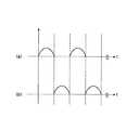
図1は、本発明の光学デバイスの第1実施形態を示す平面図(内部透視図)、図2は、図1中のA−A線断面図、図3は、図1に示す光学デバイスの電極の配置を示す平面図、図4は、図1に示す光学デバイスの駆動電圧の一例(交流電圧)を示す図、図5は、印加した交流電圧の周波数と、第1の質量部および第2の質量部の振幅との関係を示すグラフである。なお、以下では、説明の便宜上、図1および図3中の紙面手前側を「上」、紙面奥側を「下」、右側を「右」、左側を「左」と言い、図2中の上側を「上」、下側を「下」、右側を「右」、左側を「左」と言う。DESCRIPTION OF EXEMPLARY EMBODIMENTS Hereinafter, preferred embodiments of an optical device, an optical scanner, and an image forming apparatus of the invention will be described with reference to the accompanying drawings.
<First Embodiment>
First, a first embodiment of the optical device of the present invention will be described.
1 is a plan view (internal perspective view) showing a first embodiment of the optical device of the present invention, FIG. 2 is a cross-sectional view taken along line AA in FIG. 1, and FIG. 3 is a diagram of the optical device shown in FIG. FIG. 4 is a diagram showing an example (AC voltage) of the driving voltage of the optical device shown in FIG. 1, and FIG. 5 is a diagram showing the frequency of the applied AC voltage, the first mass part and the first mass part. It is a graph which shows the relationship with the amplitude of 2 mass parts. In the following, for convenience of explanation, the front side of the page in FIGS. 1 and 3 is referred to as “up”, the back side of the page is referred to as “down”, the right side is referred to as “right”, and the left side is referred to as “left”. The upper side is called “upper”, the lower side is called “lower”, the right side is called “right”, and the left side is called “left”.
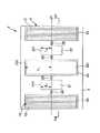
光学デバイス1は、図1に示すように、2自由度振動系を有する基体2を有しており、この基体2の下面には、対向基板3が接合層4を介して接合され、この基体2の上面には、冷却手段10が取り付けられている。
基体2は、一対の第1の質量部(駆動部)21、22と、上面(後述する対向基板3とは反対側の面)に光反射部231が設けられた第2の質量部(可動部)23と、これらを支持するための支持部24とを備えている。As shown in FIG. 1, the optical device 1 has a
The
具体的には、基体2は、第2の質量部23を中心として、その一端側(図1および図2中、左側)に第1の質量部21が設けられ、他端側(図1および図2中、右側)に第1の質量部22が設けられて構成されている。
また、本実施形態では、第1の質量部21、22は、互いにほぼ同一形状かつほぼ同一寸法をなし、第2の質量部23を介して、ほぼ対称に設けられている。Specifically, the
In the present embodiment, the
また、第2の質量部23上には、後に詳述する冷却手段10の高熱伝導膜11を介して、光反射部231が設けられている。
さらに、基体2は、図1および図2に示すように、第1の質量部21、22と支持部24とを連結する一対の第1の弾性連結部25、25と、第1の質量部21、22と第2の質量部23とを連結する一対の第2の弾性連結部26、26とを備えている。
各第1の弾性連結部25、25および各第2の弾性連結部26、26は、同軸的に設けられており、これらを回動中心軸(回転軸)27として、第1の質量部21、22が支持部24に対して、また、第2の質量部23が第1の質量部21、22に対して回動可能となっている。Further, on the
Further, as shown in FIGS. 1 and 2, the
The first elastic connecting
このように、基体2は、第1の質量部21、22と第1の弾性連結部25、25とからなる第1の振動系と、第2の質量部23と第2の弾性連結部26、26とからなる第2の振動系とで構成された2自由度振動系を有している。
本実施形態では、このような2自由度振動系は、基体2の全体の厚さよりも薄く形成されているとともに、図2にて上下方向で基体2の上部に位置している。換言すれば、基体2には、基体2の全体の厚さよりも薄い部分(以下、薄肉部という)が形成されており、この薄肉部に異形孔が形成されることにより、第1の質量部21、22と第2の質量部23と第1の弾性連結部25、25と第2の弾性連結部26、26とが形成されている。As described above, the
In the present embodiment, such a two-degree-of-freedom vibration system is formed thinner than the entire thickness of the
また、本実施形態では、前記薄肉部の上面が支持部24の上面と同一面上に位置することにより、前記薄肉部の下方には、各質量部21、22、23の回動のための空間(凹部)28が形成される。
このような基体2は、例えば、シリコンを主材料として構成されていて、第1の質量部21、22と、第2の質量部23と、支持部24と、第1の弾性連結部25、25と、第2の弾性連結部26、26とが一体的に形成されている。
なお、基体2は、SOI基板等の積層構造の基板から、第1の質量部21、22と、第2の質量部23と、支持部24と、第1の弾性連結部25、25と、第2の弾性連結部26、26を形成したものであってもよい。Moreover, in this embodiment, when the upper surface of the said thin part is located on the same surface as the upper surface of the
Such a
Note that the
対向基板3は、例えば、シリコンまたはガラスを主材料として構成されている。
対向基板3の上面には、図2および図3に示すように、第2の質量部23に対応する部分に開口部31が形成されている。
この開口部31は、第2の質量部23が回動(振動)する際に、対向基板3に接触するのを防止する逃げ部を構成する。開口部(逃げ部)31を設けることにより、光学デバイス1全体の大型化を防止しつつ、第2の質量部23の振れ角(振幅)をより大きく設定することができる。光学デバイス1において、対向基板3がシリコンを主材料として構成されている場合、ガラス材料などで対向基板が構成されている場合に比し、前述のような開口部などの逃げ部を簡単にそして高精度(高アスペクト比)に形成することができる。The
As shown in FIGS. 2 and 3, an
The
なお、逃げ部は、前記効果を十分に発揮し得る構成であれば、必ずしも対向基板3の下面(第2の質量部23と反対側の面)で開放(開口)していなくてもよい。すなわち、逃げ部は、対向基板3の上面に形成された凹部で構成することもできる。また、空間28の深さが第2の質量部23の振れ角(振幅)に対し大きい場合などには、逃げ部を設けなくともよい。 Note that the relief portion does not necessarily have to be opened (opened) on the lower surface (the surface opposite to the second mass portion 23) of the
また、対向基板3の上面(基体2側の面)には、図3に示すように、第1の質量部21に対応する部分に、後述の接合層4を介して、一対の電極32が回動中心軸27を中心にほぼ対称となるように設けられ、また、第1の質量部22に対応する部分に、後述の接合層4を介して、一対の電極32が回動中心軸27を中心にほぼ対称となるように設けられている。すなわち、本実施形態では、一対の電極32が2組(合計4個)、設けられている。 Further, as shown in FIG. 3, a pair of
第1の質量部21、22と各電極32とは、図示しない電源に接続されており、第1の質量部21、22と各電極32との間に交流電圧(駆動電圧)を印加できるよう構成されている。すなわち、第1の質量部21、22と各電極32とが、第2の質量部23(より具体的には第1の質量部21、22)を駆動するための駆動手段を構成する。
なお、第1の質量部21、22は、各電極32と対向する面に、それぞれ、絶縁膜(図示せず)が設けられている。これにより、第1の質量部21、22と各電極32との間での短絡が発生するのが好適に防止される。The
In addition, the
接合層4は、基体2と対向基板3とを接合する機能を有するものである。したがって、接合層4の構成材料は、前記接合が可能なものであれば特に限定されないが、基体2および対向基板3のそれぞれがシリコンを主材料として構成されている場合には、可動イオンを含むガラスを用いるのが好ましい。これにより、ともにシリコンを主材料として構成された基体2と対向基板3とを接合層4を介して陽極接合させることができる。
また、本実施形態では、接合層4の上面に上述の電極32が設けられている。これにより、電極32と第1の質量部21、22との間のギャップを調整することができる。また、接合層4を絶縁性を有する材料で構成することにより、電極32と対向基板3との間の絶縁性を確保することができる。The
In the present embodiment, the above-described
ここで、前述したような基体2の上面に設けられた冷却手段10を詳細に説明する。
冷却手段10は、可動部である第2の質量部23を冷却する機能を有する。これにより、第2の質量部23の昇温を防止することができる。その結果、昇温による第2の質量部23の変形や第2の弾性連結部26のバネ定数の変化を防止して、光学デバイス1の駆動を安定化することができる。Here, the cooling means 10 provided on the upper surface of the
The cooling means 10 has a function of cooling the second
より具体的には、冷却手段10は、第2の質量部23の上面に設けられた高熱伝導膜11と、高熱伝導膜11に接続されたヒートシンク12とを有している。
高熱伝導膜11は、可動部である第2の質量部23の本体上に設けられている。
そして、高熱伝導膜11は、第2の質量部23(第2の質量部23の本体)の構成材料(すなわち基体2の構成材料)の熱伝導率よりも高い熱伝導率を有する材料(以下、高熱伝導材料という)で構成されている。したがって、この高熱伝導膜11を介して第2の質量部23を放熱することができる。これにより、第2の質量部23の熱を高熱伝導膜11を通じて第2の質量部23の外部へ積極的に放熱して、第2の質量部23を冷却することができる。そのため、比較的簡単な構成で、第2の質量部23の昇温を防止することができる。More specifically, the cooling means 10 includes a high heat
The high thermal
The high thermal
特に、本実施形態では、高熱伝導膜11は、第2の質量部23の本体と光反射部231との間に介在している。これにより、光反射部231に照射された光のうち、光反射部231で反射せずに熱となったものを、第2の質量部23に伝達される前に、高熱伝導膜11を通じて外部へ放熱することができる。そのため、比較的簡単な構成で、第2の質量部23の昇温をより確実に防止することができる。 In particular, in the present embodiment, the high thermal
また、高熱伝導膜11は、第2の質量部23の一方の面のほぼ全域を覆うように設けられている。これにより、第2の質量部23の面のほぼ全域において第2の質量部23の熱を高熱伝導膜11を通じて第2の質量部23の外部へ積極的に放熱することができる。そのため、第2の質量部23の昇温をより確実に防止することができる。なお、高熱伝導膜を第2の質量部23の両面に設けてもよく、高熱伝導膜を第2の質量部23の他方の面のみに設けてもよい。 The high thermal
このような高熱伝導材料としては、特に限定されないが、例えば、Li、Be、B、Na、Mg、Al、K、Ca、Sc、V、Cr、Mn、Fe、Co、Ni、Cu、Zn、Ga、Rb、Sr、Y、Zr、Nb、Mo、Cd、In、Sn、Sb、Cs、Ba、La、Hf、Ta、W、Tl、Pb、Bi、Ce、Pr、Nd、Pm、Sm、Eu、Gd、Tb、Dy、Ho、Er、Tm、Yb、Lu、Ag、Au、Pt、Pdのような金属(金属単体)、これらの金属を含む合金、これらの金属を含む酸化物や窒化物等が挙げられる。
これらの中でも、高熱伝導性材料としては、アルミニウム、銅、チタン、ステンレス鋼のような金属材料、窒化アルミニウム、窒化ケイ素等のセラミックス材料が好ましい。Such a high thermal conductive material is not particularly limited, but, for example, Li, Be, B, Na, Mg, Al, K, Ca, Sc, V, Cr, Mn, Fe, Co, Ni, Cu, Zn, Ga, Rb, Sr, Y, Zr, Nb, Mo, Cd, In, Sn, Sb, Cs, Ba, La, Hf, Ta, W, Tl, Pb, Bi, Ce, Pr, Nd, Pm, Sm, Metals such as Eu, Gd, Tb, Dy, Ho, Er, Tm, Yb, Lu, Ag, Au, Pt, Pd, alloys containing these metals, oxides and nitridings containing these metals Thing etc. are mentioned.
Among these, as the high thermal conductivity material, metal materials such as aluminum, copper, titanium, and stainless steel, and ceramic materials such as aluminum nitride and silicon nitride are preferable.
ヒートシンク12は、放熱のための複数のフィンを有しており、外部の気体との接触面積の向上が図られており、高熱伝導膜11から熱を受けこれを放熱する機能を有する。
このように冷却手段10が高熱伝導膜11に接続されたヒートシンク12を有しているので、高熱伝導膜11に伝達された熱をヒートシンク12からより積極的に放熱することができる。そのため、第2の質量部23の昇温をより確実に防止することができる。The
Thus, since the cooling means 10 has the
また、ヒートシンク12は、支持部24上に設けられている。このように第2の質量部23と一体的に形成された部分の上にヒートシンク12が設けられているので、第2の質量部23と一体的に形成された部分、より具体的には、基体2全体の熱を下げて、第2の質量部23の昇温をより確実に防止することができる。
このようなヒートシンク12は、第2の質量部23の構成材料(すなわち基体2の構成材料)の熱伝導率よりも高い熱伝導率を有する材料(以下、高熱伝導材料という)で構成されている。したがって、ヒートシンク12の構成材料としては、前述した高熱伝導材料と同様のものを用いることができる。
なお、本実施形態ではヒートシンク12は高熱伝導膜11と別体として形成されているが、ヒートシンク12と高熱伝導膜11とが一体となっていてもよい。The
Such a
In the present embodiment, the
以上のような構成の光学デバイス1は、次のようにして駆動する。
すなわち、第1の質量部21、22と各電極32との間に、例えば、正弦波(交流電圧)等を印加する。具体的には、例えば、第1の質量部21、22をアースしておき、図3中上側の2つの電極32に、図4(a)に示すような波形の電圧を印加し、図3中下側の2つの電極32に、図4(b)に示すような波形の電圧を印加する。すると、第1の質量部21、22と各電極32との間に静電気力(クーロン力)が生じる。The optical device 1 having the above configuration is driven as follows.
That is, for example, a sine wave (AC voltage) or the like is applied between the
この静電気力により、第1の質量部21、22が、各電極32の方へ引きつけられる力が正弦波の位相により変化し、回動中心軸27(第1の弾性連結部25)を軸に、基体2の板面(図1における紙面)に対して傾斜するように振動(回動)する。
そして、この第1の質量部21、22の振動(駆動)に伴って、第2の弾性連結部26を介して連結されている第2の質量部23も、回動中心軸27(第2の弾性連結部26)を軸に、基体2の板面(図1における紙面)に対して傾斜するように振動(回動)する。Due to this electrostatic force, the force that the first
The
したがって、第2の質量部23の回動に伴い、光反射部231も回動し、光反射部231に照射された光を走査することができる。
その際、光反射部231に照射された光の一部は、光反射部231で反射せずに熱となる。この熱は、高熱伝導膜11を通じて、ヒートシンク12へ伝導し、外部へ放出される。これにより、光反射部231で生じた熱により第2の質量部23が昇温するのを防止することができる。そのため、光学デバイス1は、第2の質量部23が昇温により反りなどの変形を生じることなく、安定に駆動して、高精度な描画や光走査を行うことができる。Therefore, as the
At that time, a part of the light applied to the
ここで、この光学デバイス1では、前述したように、対向基板3における、第2の質量部23に対応する部分に、開口部31が形成され、また、図2にて基体2の下面に空間28が形成され、かつ、平面視で第1の質量部21、22が空間(凹部)28内に位置するように設けられている。
このような構成により、第2の質量部23が振動し得るスペース、および、第1の質量部21、22が振動し得るスペースとして、大きなスペースが確保されている。したがって、第1の質量部21、22の質量を比較的小さく設定すること等により、第1の質量部21、22を大きな振れ角で振動させた場合や、さらに第2の質量部23が共振によって大きな振れ角で振動した場合でも、各質量部21、22、23(2自由度振動系)が対向基板3に接触することを好適に防止することができる。Here, in the optical device 1, as described above, the
With such a configuration, a large space is secured as a space where the
このため、このような光学デバイス1を、例えば光スキャナに適用した場合には、より解像度の高いスキャニングを行うことが可能となる。なお、光学デバイス1は、光スキャナのほか、光スイッチ、光アッテネータなどの他の光学デバイスとしても用いることができる。このような他の光学デバイスとして光学デバイス1を用いた場合、スイッチング特性や、光の減衰特性を長期に亘り安定化させることができる。 For this reason, when such an optical device 1 is applied to, for example, an optical scanner, it is possible to perform scanning with higher resolution. In addition to the optical scanner, the optical device 1 can be used as another optical device such as an optical switch or an optical attenuator. When the optical device 1 is used as such another optical device, switching characteristics and light attenuation characteristics can be stabilized over a long period of time.
ここで、第1の質量部21の回動中心軸からこれにほぼ垂直な方向(長手方向)への長さ(回動中心軸と端部211との間の距離)をL1とし、第1の質量部22の回動中心軸からこれにほぼ垂直な方向(長手方向)への長さ(回動中心軸と端部221との間の距離)をL2とし、第2の質量部23の回動中心軸からこれにほぼ垂直な方向への長さ(回動中心軸と端部232との間の距離)をL3としたとき、本実施形態では、第1の質量部21、22が、それぞれ独立して設けられているため、第1の質量部21、22と、第2の質量部23とが干渉せず、第2の質量部23の大きさ(長さL3)にかかわらず、L1およびL2を小さくすることができる。これにより、第1の質量部21、22の回転角度(振れ角)を大きくすることができ、第2の質量部23の回転角度を大きくすることができる。Here, the length of a direction substantially perpendicular to the rotational axis of the first mass portion 21 (longitudinal direction) (the distance between the rotational axis and the edge 211) and L1, the substantially perpendicular from the rotation center axis of the
また、L1およびL2を小さくすることにより、第1の質量部21、22と各電極32との間の距離を小さくすることができ、これにより、静電気力が大きくなり、第1の質量部21、22と各電極32に印加する交流電圧を小さくすることができる。
ここで、第1の質量部21、22および第2の質量部23の寸法は、それぞれ、L1<L3かつL2<L3なる関係を満足するよう設定されている。これにより、L1およびL2をより小さくすることができ、第1の質量部21、22の回転角度をより大きくすることができ、第2の質量部23の回転角度をさらに大きくすることができる。In addition, by reducing L1 and L2 , the distance between the
Here, the dimension of the first
この場合、第2の質量部23の最大回転角度が、20°以上となるように構成されるのが好ましい。
また、このように、L1およびL2を小さくすることにより、第1の質量部21、22と各電極32との間の距離をより小さくすることができ、第1の質量部21、22と各電極32に印加する交流電圧をさらに小さくすることができる。In this case, it is preferable that the maximum rotation angle of the
In addition, by reducing L1 and L2 in this way, the distance between the
これらによって、第1の質量部21、22の低電圧駆動と、第2の質量部23の大回転角度での振動(回動)とを実現することができる。
このため、このような光学デバイス1を、例えばレーザープリンタや、走査型共焦点レーザー顕微鏡等の装置に用いられる光スキャナに適用した場合には、より容易に装置の小型化を図ることができる。By these, the low voltage drive of the
For this reason, when such an optical device 1 is applied to an optical scanner used in an apparatus such as a laser printer or a scanning confocal laser microscope, the apparatus can be more easily downsized.
なお、前述したように、本実施形態では、L1とL2とはほぼ等しく設定されているが、L1とL2とが異なっていてもよいことは言うまでもない。
ところで、このような質量部21、22、23よりなる振動系(2自由度振動系)では、第1の質量部21、22および第2の質量部23の振幅(振れ角)と、印加する交流電圧の周波数との間に、図5に示すような周波数特性が存在している。As described above, in the present embodiment, L1 and L2 are set to be substantially equal, but it goes without saying that L1 and L2 may be different.
By the way, in such a vibration system (two-degree-of-freedom vibration system) composed of the
すなわち、かかる振動系は、第1の質量部21、22の振幅と、第2の質量部23の振幅とが大きくなる2つの共振周波数fm1[kHz]、fm3[kHz](ただし、fm1<fm3)と、第1の質量部21、22の振幅がほぼ0となる、1つの反共振周波数fm2[kHz]とを有している。
この振動系では、第1の質量部21、22と電極32との間に印加する交流電圧の周波数Fが、2つの共振周波数のうち低いもの、すなわち、fm1とほぼ等しくなるように設定するのが好ましい。これにより、第1の質量部21、22の振幅を抑制しつつ、第2の質量部23の振れ角(回転角度)を大きくすることができる。
なお、本明細書中では、F[kHz]とfm1[kHz]とがほぼ等しいとは、(fm1−1)≦F≦(fm1+1)の条件を満足することを意味する。That is, the vibration system includes two resonance frequencies fm1 [kHz] and fm3 [kHz] (however, fm) in which the amplitude of the
In this vibration system, the frequency F of the alternating voltage applied between the
In the present specification, F [kHz] and fm1 [kHz] being substantially equal means that the condition of (fm1 −1) ≦ F ≦ (fm1 +1) is satisfied.
第1の質量部21、22の平均厚さは、それぞれ、1〜1500μmであるのが好ましく、10〜300μmであるのがより好ましい。
第2の質量部23の平均厚さは、1〜1500μmであるのが好ましく、10〜300μmであるのがより好ましい。
第1の弾性連結部25のばね定数k1は、1×10⁻⁴〜1×10⁴Nm/radであるのが好ましく、1×10−2〜1×103Nm/radであるのがより好ましく、1×10−1〜1×102Nm/radであるのがさらに好ましい。これにより、第2の質量部23の回転角度(振れ角)をより大きくすることができる。The average thicknesses of the
The average thickness of the second
The spring constant k1 of the first elastic connecting
一方、第2の弾性連結部26のばね定数k2は、1×10⁻⁴〜1×10⁴Nm/radであるのが好ましく、1×10−2〜1×103Nm/radであるのがより好ましく、1×10−1〜1×102Nm/radであるのがさらに好ましい。これにより、第1の質量部21、22の振れ角を抑制しつつ、第2の質量部23の振れ角をより大きくすることができる。On the other hand, the spring constant k2 of the second
また、第1の弾性連結部25のばね定数k1と第2の弾性連結部26のばね定数をk2とは、k1>k2なる関係を満足するのが好ましい。これにより、第1の質量部21、22の振れ角を抑制しつつ、第2の質量部23の回転角度(振れ角)をより大きくすることができる。
さらに、第1の質量部21、22の慣性モーメントをJ1とし、第2の質量部23の慣性モーメントをJ2としたとき、J1とJ2とは、J1≦J2なる関係を満足することが好ましく、J1<J2なる関係を満足することがより好ましい。これにより、第1の質量部21、22の振れ角を抑制しつつ、第2の質量部23の回転角度(振れ角)をより大きくすることができる。Further, the spring constantk 1 of the first elastic connecting
Furthermore, the moment of inertia of the first
ところで、第1の質量部21、22と第1の弾性連結部25、25とからなる第1の振動系の固有振動数ω1は、第1の質量部21、22の慣性モーメントJ1と、第1の弾性連結部25のばね定数k1とにより、ω1=(k1/J1)1/2によって与えられる。一方、第2の質量部23と第2の弾性連結部26、26とからなる第2の振動系の固有振動数ω2は、第2の質量部23の慣性モーメントJ2と、第2の弾性連結部26のばね定数k2とにより、ω2=(k2/J2)1/2によって与えられる。By the way, the natural frequency ω1 of the first vibration system including the
このようにして求められる第1の振動系の固有振動数ω1と第2の振動系の固有振動数ω2とは、ω1>ω2なる関係を満足するのが好ましい。これにより、第1の質量部21、22の振れ角を抑制しつつ、第2の質量部23の回転角度(振れ角)をより大きくすることができる。
なお、本実施形態の振動系は、一対の第1の弾性連結部25および一対の第2の弾性連結部26のうち少なくとも1つの内部にピエゾ抵抗素子を設けることにより、例えば、回転角度および回転周波数を検出したりすることができ、また、その検出結果を、第2の質量部23の姿勢の制御に利用することができる。It is preferable that the natural frequency ω1 of the first vibration system and the natural frequency ω2 of the second vibration system thus obtained satisfy the relationship ω1 > ω2 . Thereby, the rotation angle (swing angle) of the
Note that the vibration system according to the present embodiment is provided with a piezoresistive element in at least one of the pair of first
このような光学デバイス1は、例えば、次のようにして製造することができる。
図6、図7は、それぞれ、第1実施形態の光学デバイスの製造方法を説明するための図(縦断面図)である。なお、以下では、説明の便宜上、図6、図7中の上側を「上」、下側を「下」と言う。Such an optical device 1 can be manufactured as follows, for example.
6 and 7 are views (longitudinal sectional views) for explaining the method of manufacturing the optical device according to the first embodiment. In the following, for convenience of explanation, the upper side in FIGS. 6 and 7 is referred to as “upper” and the lower side is referred to as “lower”.
[A1] まず、図6(a)に示すように、シリコン基板5を用意する。
次に、シリコン基板5の一方の面に、図6(b)に示すように、支持部24と各質量部21、22、23との形状に対応するように、例えば、アルミニウム等により金属マスク6を形成する。
そして、図6(c)に示すように、シリコン基板5の他方の面に、フォトレジストを塗布し、露光、現像を行う。これにより、図6(c)に示すように、支持部24の形状に対応するように、レジストマスク7を形成する。なお、レジストマスク7の形成は、金属マスク6の形成よりも先に行ってもよい。[A1] First, as shown in FIG. 6A, a
Next, on one surface of the
Then, as shown in FIG. 6C, a photoresist is applied to the other surface of the
金属マスク6の形成方法としては、真空蒸着、スパッタリング(低温スパッタリング)、イオンプレーティング等の乾式メッキ法、電解メッキ、無電解メッキ等の湿式メッキ法、溶射法、金属箔の接合等が挙げられる。なお、以下の各工程における金属膜の成膜においても、同様の方法を用いることができる。
次に、このレジストマスク7を介して、シリコン基板5の前記他方の面をエッチングした後、レジストマスク7を除去する。これにより、図6(d)に示すように、支持部24に対応する部分以外の領域に凹部51が形成される。Examples of the method for forming the metal mask 6 include vacuum plating, sputtering (low temperature sputtering), dry plating methods such as ion plating, wet plating methods such as electrolytic plating and electroless plating, thermal spraying methods, joining metal foils, and the like. . Note that the same method can also be used for forming a metal film in the following steps.
Next, after etching the other surface of the
エッチング方法としては、例えば、プラズマエッチング、リアクティブイオンエッチング、ビームエッチング、光アシストエッチング等の物理的エッチング法、ウェットエッチング等の化学的エッチング法等のうちの1種または2種以上を組み合わせて用いることができる。なお、以下の各工程におけるエッチングにおいても、同様の方法を用いることができる。 As an etching method, for example, one or more of physical etching methods such as plasma etching, reactive ion etching, beam etching, and light-assisted etching, and chemical etching methods such as wet etching are used in combination. be able to. Note that the same method can be used for etching in the following steps.
次に、金属マスク6を介して、シリコン基板5の前記一方の面側を、前記凹部51に対応する部分が貫通するまでエッチングする。
そして、金属マスク6を除去した後、図6(e)に示すように、第2の質量部23上に高熱伝導膜11を形成し、次いで、ヒートシンク12を設けるとともに光反射部231を形成する。Next, the one surface side of the
Then, after removing the metal mask 6, as shown in FIG. 6E, the high thermal
高熱伝導膜11の形成方法としては、前述した金属マスク6の形成方法と同様のものを用いることができる。
なお、ここで、シリコン基板5をエッチングを行った後、金属マスク6を除去せずに残存させ、高熱伝導膜11の一部として用いることができる。
以上の工程により、図6(e)に示すように、各質量部21、22、23および支持部24が一体的に形成された基体2上に冷却手段10が形成された構造体が得られる。As a method for forming the high thermal
Here, after the
Through the above steps, as shown in FIG. 6E, a structure in which the cooling means 10 is formed on the
[A2] 次に、図7(a)に示すように、対向基板3を形成するためのシリコン基板9を用意する。
そして、シリコン基板9の一方の面に、開口部31を形成する領域を除いた部分に対応するように、例えば、アルミニウム等により金属マスクを形成する。
次に、この金属マスクを介して、シリコン基板9の一方の面側をエッチングした後、金属マスクを除去する。これにより、開口部31が形成された対向基板3が得られる。[A2] Next, as shown in FIG. 7A, a silicon substrate 9 for forming the
Then, a metal mask is formed on one surface of the silicon substrate 9 with, for example, aluminum so as to correspond to a portion excluding the region where the
Next, after etching one surface side of the silicon substrate 9 through the metal mask, the metal mask is removed. Thereby, the
しかる後に、例えば可動イオンを含むガラスで対向基板3の一方の面に成膜して、図7(b)に示すように、対向基板3上に接合層4を形成する。
次に、接合層4上に、図7(c)に示すように、電極32を形成する。これにより、接合層4の厚さを調整することで、電極32と第1の質量部21、22との間のギャップを調整することができる。Thereafter, a film is formed on one surface of the
Next, an
電極32は、接合層4に金属膜を成膜し、電極32の形状に対応するマスクを介して金属膜をエッチングを行った後、マスクを除去することにより形成することができる。
次に、図7(d)に示すように、前記工程[A1]で得られた構造体と、前記工程[A2]で接合層4が成膜された対向基板3とを、例えば陽極接合により接合して光学デバイス1を得る。
以上のようにして、第1実施形態の光学デバイス1が製造される。The
Next, as shown in FIG. 7D, the structure obtained in the step [A1] and the
As described above, the optical device 1 of the first embodiment is manufactured.
<第2実施形態>
次に、本発明の光学デバイスの第2実施形態について説明する。
図8は、本発明の光学デバイスの第2実施形態を示す平面図(内部透視図)、図9は、図8中のA−A線断面図である。
本実施形態にかかる光学デバイス1Aは、冷却手段の構成が異なる以外は、前述した第1実施形態にかかる光学デバイス1と同様である。Second Embodiment
Next, a second embodiment of the optical device of the present invention will be described.
FIG. 8 is a plan view (internal perspective view) showing a second embodiment of the optical device of the present invention, and FIG. 9 is a cross-sectional view taken along line AA in FIG.
The
図8および図9に示すように、本実施形態の光学デバイス1Aにおいては、第2の質量部23の本体上に高熱伝導膜11Aが設けられ、この高熱伝導膜11Aは、光反射部を兼ねている。これにより、光学デバイス1Aの製造時において、一回の成膜工程により高熱伝導膜11Aと光反射部とを形成することができ、光学デバイス1Aの低コスト化を図ることができる。 As shown in FIGS. 8 and 9, in the
このような高熱伝導膜11Aには、ヒートシンク12Aが接続されている。このヒートシンク12Aは、駆動部である第1の質量部21、22の上に設けられている。これにより、駆動時にヒートシンク12Aとその周囲の気体との接触確率を向上して、可動部である第2の質量部23の冷却効果をより高めることができる。
特に、ヒートシンク12Aには、第1の質量部21、22の回動軸線に対し直角な方向に延びるフィン12A1が前記回動軸線方向に間隔を隔てて設けられている。これにより、ヒートシンク12Aとその周囲との気体との接触抵抗を低減しつつ、第2の質量部23の冷却効果を高めることができる。A
In particular, the
また、ヒートシンク12Aは、第1の質量部21、22の回動軸線に対し直角な方向において端部側の高さが中央部側の高さよりも低い。これにより、第1の質量部21、22の回動軸線に直角な方向での端部の駆動時における慣性力を低減し、第1の質量部21、22の設計を容易なものとすることができる。
特に、ヒートシンク12Aは、第1の質量部21、22の回動軸線に対し直角な方向での中央部、すなわち端部を除く領域に設けられているので、第1の質量部21、22の回動軸線に直角な方向での端部の駆動時における慣性力をより低減することができる。Further, the
In particular, since the
また、本実施形態では、第2の質量部23の本体と高熱伝導膜11Aとの間に、高熱伝導膜11Aの構成材料よりも熱伝導率の低い低熱伝導膜13が介在している。これにより、光反射部231で生じた熱を高熱伝導膜11Aを通じて第2の質量部23の外部へ放出するとともに、高熱伝導膜11Aで放出しきれなかった熱を低熱伝導膜13に一時的に蓄積することができる。そして、低熱伝導膜13に蓄積された熱は、高熱伝導膜11Aを通じて第2の質量部23の外部へ放出される。そのため、光反射部231で生じた熱が第2の質量部23へ伝達されるのをより確実に防止しつつ、第2の質量部23の冷却を行うことができる。 In the present embodiment, the low thermal
なお、前述した第1実施形態のように光反射部231と高熱伝導膜11とが別体である場合、前述したような低熱伝導膜を光反射部231と高熱伝導膜11との間に介在させることができる。この場合には、光反射部231で生じた熱は、低熱伝導膜に一旦蓄積された後に、高熱伝導膜11を通じて第2の質量部23の外部へ放出される。そのため、光反射部231で生じた熱が第2の質量部23へ伝達されるのをより確実に防止しつつ、第2の質量部23の冷却を行うことができる。 When the
以上説明したような光学デバイス1、1Aは、それぞれ、例えば、レーザープリンタ、バーコードリーダー、走査型共焦点レーザー顕微鏡、イメージング用ディスプレイ等の画像形成装置に用いる光スキャナに好適に適用することができる。光スキャナとして本発明にかかる光学デバイス1、1Aを備えた画像形成装置は、第2の質量部23の昇温を防止することができるため、安定した駆動を行うこと(長期に亘り高品位な画像を得ること)ができる。 The
ここで、図10ないし図12に基づき、光学デバイス1を備えた画像形成装置、すなわち本発明の画像形成装置の具体例を説明する。
まず、電子写真方式を採用するプリンタに本発明を適用した例を説明する。
図10は、本発明の光スキャナを備える画像形成装置(プリンタ)の一例を示す全体構成の模式的断面図である。Here, a specific example of the image forming apparatus including the optical device 1, that is, the image forming apparatus of the present invention will be described with reference to FIGS.
First, an example in which the present invention is applied to a printer that employs an electrophotographic system will be described.
FIG. 10 is a schematic cross-sectional view of the overall configuration showing an example of an image forming apparatus (printer) including the optical scanner of the present invention.
図10に示す画像形成装置110(プリンタ)は、露光・現像・転写・定着を含む一連の画像形成プロセスによって、トナーからなる画像を紙やOHPシートなどの記録媒体に記録するものである。このような画像形成装置110は、図10に示すように、図示矢印方向に回転する感光体111を有し、その回転方向に沿って順次、帯電ユニット112、露光ユニット113、現像ユニット114、転写ユニット115、クリーニングユニット116が配設されている。また、画像形成装置110は、図10にて、下部に、紙などの記録媒体Pを収容する給紙トレイ117が設けられ、上部に、定着装置118が設けられている。 An image forming apparatus 110 (printer) shown in FIG. 10 records an image made of toner on a recording medium such as paper or an OHP sheet by a series of image forming processes including exposure, development, transfer, and fixing. As shown in FIG. 10, such an
感光体111は、例えば、円筒状の導電性基材(図示せず)の外周面に感光層(図示せず)を形成してなり、その軸線まわりに回転可能となっている。
帯電ユニット112は、コロナ帯電などにより感光体111の表面を一様に帯電するための装置である。
露光ユニット113は、図示しないパーソナルコンピュータなどのホストコンピュータから画像情報を受けこれに応じて、一様に帯電された感光体111上に、レーザーを選択的に照射することによって、静電的な潜像を形成する装置である。The
The charging
The
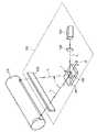
より具体的に説明すると、露光ユニット113は、図11に示すように、光スキャナである光学デバイス1と、レーザー光源131と、コリメータレンズ132と、fθレンズ133とを有している。
このような露光ユニット113にあっては、レーザー光源131からコリメータレンズ132を介して光学デバイス1(光反射部251)にレーザー光Lが照射される。そして、光反射部251で反射したレーザー光Lがfθレンズを介して感光体111上に照射される。More specifically, the
In such an
その際、光学デバイス1の駆動(第2の質量部25の回動中心軸Xまわりの回動)により、光反射部251で反射した光(レーザーL)は、感光体111の軸線方向に走査(主走査)される。一方、感光体111の回転により、光反射部251で反射した光(レーザーL)は、感光体111の周方向に走査(副走査)される。また、レーザー光源131から出力されるレーザー光Lの強度は、図示しないホストコンピュータから受けた画像情報に応じて変化する。
このようにして露光ユニット113は、感光体111上を選択的に露光して画像形成(描画)を行う。At that time, the light (laser L) reflected by the
In this way, the
現像ユニット114は、4つの現像装置141、142、143、144と、これらの現像装置を保持する保持体145を有し、保持体145を軸146まわりに回転させることにより、各現像装置を感光体111に選択的に対向させるようになっている。ここで、現像装置141はブラック(K)トナー用の現像装置、現像装置142はマゼンタ(M)トナー用の現像装置、現像装置143はシアン(C)トナー用の現像装置、現像装置144はイエロー(Y)トナー用の現像装置である。 The developing
転写ユニット115は、エンドレスベルト状の中間転写ベルト151と、この中間転写ベルト151を張架する3つのローラ(一次転写ローラ152、従動ローラ153、駆動ローラ154)と、中間転写ベルト151を介して駆動ローラ154に対向する二次転写ローラ155とを有している。
中間転写ベルト151は、駆動ローラ154の回転により、一次転写ローラ152および従動ローラ153を従動回転させながら、図10に示す矢印方向に、感光体111とほぼ同じ周速度にて回転駆動されるようになっている。The
The
一次転写ローラ152は、感光体111に形成された単色のトナー像を中間転写ベルト151に転写するための装置である。
二次転写ローラ155は、中間転写ベルト151上に形成された単色やフルカラーなどのトナー像を、紙、フィルム、布等の記録媒体Pに転写するための装置である。
定着装置118は、前記トナー像の転写を受けた記録媒体Pを加熱および加圧することにより、前記トナー像を記録媒体Pに融着させて永久像として定着させるための装置である。The
The
The fixing
クリーニングユニット116は、一次転写ローラ152と帯電ユニット12との間で感光体111の表面に当接するゴム製のクリーニングブレード161を有し、一次転写ローラ152によって中間転写ベルト151上にトナー像が転写された後に、感光体111上に残存するトナーをクリーニングブレード161により掻き落として除去するための装置である。 The
このような画像形成装置110にあっては、まず、図示しないホストコンピュータからの指令により、感光体111、現像ユニット114に設けられた現像ローラ(図示せず)、および中間転写ベルト151が回転を開始する。そして、感光体111は、回転しながら、帯電ユニット112により順次帯電される。
感光体111の帯電された領域は、感光体111の回転に伴って露光位置に至り、露光ユニット113によって、第1色目、例えばイエローYの画像情報に応じた潜像が前記領域に形成される。In such an
The charged region of the
感光体111上に形成された潜像は、感光体111の回転に伴って現像位置に至り、イエロー現像のための現像装置144によってイエロートナーで現像される。これにより、感光体111上にイエロートナー像が形成される。このとき、現像ユニットは、現像装置144が、前記現像位置にて感光体111と対向している。
感光体111上に形成されたイエロートナー像は、感光体111の回転に伴って一次転写位置(すなわち、感光体111と一次転写ローラ152との対向部)に至り、一次転写ローラ152によって、中間転写ベルト151に転写(一次転写)される。このとき、一次転写ローラ152には、トナーの帯電極性とは逆の極性の一次転写電圧(一次転写バイアス)が印加される。なお、この間、二次転写ローラ155は、中間転写ベルト151から離間している。
前述の処理と同様の処理が、第2色目、第3色目および第4色目について繰り返して実行されることにより、各画像信号に対応した各色のトナー像が、中間転写ベルト151に重なり合って転写される。これにより、中間転写ベルト151上にはフルカラートナー像が形成される。The latent image formed on the
The yellow toner image formed on the
The same processing as described above is repeatedly executed for the second color, the third color, and the fourth color, so that the toner images of the respective colors corresponding to the respective image signals are transferred onto the
一方、記録媒体Pは、給紙トレイ117から、給紙ローラ171、レジローラ172によって二次転写位置(すなわち、二次転写ローラと駆動ローラとの対向部)へ搬送される。
中間転写ベルト151上に形成されたフルカラートナー像は、中間転写ベルト151の回転に伴って二次転写位置に至り、二次転写ローラ155によって記録媒体Pに転写(二次転写)される。このとき、二次転写ローラ155は中間転写ベルト151に押圧されるとともに二次転写電圧(二次転写バイアス)が印加される。On the other hand, the recording medium P is conveyed from the
The full color toner image formed on the
記録媒体Pに転写されたフルカラートナー像は、定着装置118によって加熱および加圧されて記録媒体Pに融着される。その後、片面プリントの場合には、記録媒体Pは、排紙ローラ対173によって画像形成装置110の外部へ排出される。
一方、感光体11は一次転写位置を経過した後に、クリーニングユニット116のクリーニングブレード161によって、その表面に付着しているトナーが掻き落とされ、次の潜像を形成するための帯電に備える。掻き落とされたトナーは、クリーニングユニット116内の残存トナー回収部に回収される。The full-color toner image transferred to the recording medium P is heated and pressurized by the fixing
On the other hand, after the primary transfer position has elapsed, the toner adhering to the surface of the
両面プリントの場合には、定着装置118によって一方の面に定着処理された記録媒体Pを一旦排紙ローラ対173により挟持した後に、排紙ローラ対173を反転駆動するとともに、搬送ローラ対174、176を駆動して、当該記録媒体Pを搬送路175を通じて表裏反転して二次転写位置へ帰還させ、前述と同様の動作により、記録媒体Pの他方の面に画像を形成する。 In the case of double-sided printing, after the recording medium P fixed on one surface by the fixing
次に、イメージングディスプレイ(表示装置)に本発明を適用した例を説明する。
図12は、本発明の画像形成装置(イメージングディスプレイ)の一例を示す概略図である。
図12に示す画像形成装置119は、光スキャナである光学デバイス1と、R(赤)、G(緑)、B(青)の3色の光源191、192、193と、クロスダイクロイックプリズム(Xプリズム)194と、ガルバノミラー195と、固定ミラー196と、スクリーン197とを備えている。Next, an example in which the present invention is applied to an imaging display (display device) will be described.
FIG. 12 is a schematic diagram illustrating an example of an image forming apparatus (imaging display) according to the present invention.
An
このような画像形成装置119にあっては、光源191、192、193からクロスダイクロイックプリズム194を介して光学デバイス1(光反射部251)に各色の光が照射される。このとき、光源191からの赤色の光と、光源192からの緑色の光と、光源193からの青色の光とが、クロスダイクロイックプリズム194にて合成される。
そして、光反射部251で反射した光(3色の合成光)は、ガルバノミラー195で反射した後に、固定ミラー196で反射し、スクリーン197上に照射される。In such an
Then, the light (three colors of combined light) reflected by the
その際、光学デバイス1の駆動(第2の質量部25の回動中心軸Xまわりの回動)により、光反射部251で反射した光は、スクリーン197の横方向に走査(主走査)される。一方、ガルバノミラー195の軸線Yまわりの回転により、光反射部251で反射した光は、スクリーン197の縦方向に走査(副走査)される。また、各色の光源191、192、193から出力される光の強度は、図示しないホストコンピュータから受けた画像情報に応じて変化する。 At that time, the light reflected by the
前述したような第1、2実施形態の光学デバイスは、2自由度振動系を有するねじり振動子を用いた光学デバイスであるため、マイクロマシン技術を用いて製造することができ、小型化を図ることができる。特に、2自由度振動系を有するねじり振動子は、駆動電圧を低減しつつ、大きな振幅で可動部(第2の質量部23)を駆動することができる。
なお、本発明は2自由度振動系以外の振動系の光学デバイスにも適用することができる。例えば、前述した第1、2実施形態において、第1の質量部および第1の弾性連結部を省略し、第2の弾性連結部により第2の質量部と支持部とを連結したような形態としてもよい。すなわち、本発明は、1自由度振動系を有するねじり振動子を用いた光学デバイスにも適用することができる。このようなねじり振動子を用いた光学デバイスにあっても、マイクロマシン技術を用いて製造することができるので、小型化を図ることができる。Since the optical device of the first and second embodiments as described above is an optical device using a torsional vibrator having a two-degree-of-freedom vibration system, it can be manufactured by using a micromachine technique and can be miniaturized. Can do. In particular, the torsional vibrator having the two-degree-of-freedom vibration system can drive the movable part (second mass part 23) with a large amplitude while reducing the drive voltage.
The present invention can also be applied to an optical device having a vibration system other than the two-degree-of-freedom vibration system. For example, in the first and second embodiments described above, the first mass part and the first elastic connecting part are omitted, and the second mass connecting part and the support part are connected by the second elastic connecting part. It is good. That is, the present invention can also be applied to an optical device using a torsional vibrator having a one-degree-of-freedom vibration system. Even an optical device using such a torsional vibrator can be manufactured using a micromachine technique, and thus can be miniaturized.
以上、本発明の光学デバイス、光スキャナ、および画像形成装置について、図示の各実施形態に基づいて説明したが、本発明はこれらに限定されるものではない。
また、例えば、本発明の光学デバイスは、第1実施形態の任意の構成と第2実施形態のの任意の構成とを組み合わせるようにしてもよい。
また、本発明の光学デバイスでは、各部の構成は、同様の機能を発揮する任意の構成のものに置換することができ、また、任意の構成を付加することもできる。While the optical device, the optical scanner, and the image forming apparatus of the present invention have been described based on the illustrated embodiments, the present invention is not limited to these.
Further, for example, the optical device of the present invention may be combined with any configuration of the first embodiment and any configuration of the second embodiment.
In the optical device of the present invention, the configuration of each part can be replaced with any configuration that exhibits the same function, and any configuration can be added.
また、前述した実施形態では、静電駆動により第1の質量部21、22を回動させ、これに伴い、第2の質量部23を回動させるもの、すなわち、可動部を駆動する駆動手段として静電駆動を用いたものを説明したが、駆動手段としては、これに限定されず、圧電駆動など他の駆動方式のものを採用することもできる。また、静電駆動を用いた駆動手段としては、前述したような平行平板型以外にも、櫛歯状電極を用いたものなど他の形態であってもよい。
また、可動部(第2の質量部)を冷却する冷却手段としては、可動部を冷却または放熱することができるものであれば、前述した実施形態のものに限定されない。In the above-described embodiment, the first
Further, the cooling means for cooling the movable part (second mass part) is not limited to the above-described embodiment as long as the movable part can be cooled or radiated.
1、1A……光学デバイス 2……基体 21、22……第1の質量部 211、221……端部 23……第2の質量部 231、251……光反射部 232……端部 24……支持部 25……第1の弾性連結部 26……第2の弾性連結部 27……回転中心軸 28……空間 3……対向基板 31……開口部 32……電極 4……接合層 5……シリコン基板 51……凹部 6……金属マスク 7……レジストマスク 9……シリコン基板 10……冷却手段 11、11A……高熱伝導膜 12、12A……ヒートシンク 12A1……フィン 13……低熱伝導膜 110、119……画像形成装置 111……感光体 112……帯電ユニット 113……露光ユニット 114……現像ユニット 115……転写ユニット 116……クリーニングユニット 117……給紙トレイ 118……定着装置 131……レーザー光源 132……コリメータレンズ 133……fθレンズ 141〜144……現像装置 145……保持体 146……軸 151……中間転写ベルト 152……一次転写ローラ 153……従動ローラ 154……駆動ローラ 155……二次転写ローラ 161……クリーニングブレード 171……給紙ローラ 172……レジローラ 173……排紙ローラ対 174、176……搬送ローラ対 175……搬送路 191〜193……光源 194……クロスダイクロイックプリズム 195……ガルバノミラー 196……固定ミラー 197……スクリーン L1、L2、L3……距離DESCRIPTION OF
Claims (9)
Translated fromJapanese前記可動部を支持するための支持部と、
前記支持部に対し前記可動部を回動可能とするように前記可動部と前記支持部とを連結する弾性連結部と、
前記可動部を駆動する駆動手段とを有し、
前記駆動手段が前記弾性連結部を捩れ変形させながら前記可動部を回動させることにより、前記光反射部で反射した光を対象物に走査する光学デバイスであって、
前記可動部を冷却する冷却手段を有し、
前記冷却手段は、前記可動部の本体上と前記支持部上とこれらの間とに連続して設けられ、前記光反射部を兼ねるとともに、前記可動部の本体を構成する材料よりも熱伝導率の高い材料で構成された高熱伝導膜と、前記支持部上にて前記高熱伝導膜に接続され、前記高熱伝導膜に伝達された熱を放熱するヒートシンクとを有することを特徴とする光学デバイス。A movable part having a light reflecting part and rotatably provided;
A support part for supporting the movable part;
An elastic connecting portion that connects the movable portion and the support portion so that the movable portion can rotate with respect to the support portion;
Driving means for driving the movable part;
An optical device that scans light reflected by the light reflecting portion onto an object by rotating the movable portionwhile the driving meanstwists and deforms the elastic connecting portion ,
A cooling means for cooling the movable part;
The cooling means is providedcontinuously on the body of the movable part, on thesupport part and between them, andalso serves as the light reflecting part, and has a thermal conductivity higher than that of the material constituting the body of the movable part. An optical device comprising: a high heat conductive film made of a high material; and a heat sink connected to the high heat conductive filmon the support portion to dissipate heat transferred to the high heat conductive film.
前記可動部を支持するための支持部と、 A support part for supporting the movable part;
前記可動部を駆動するための駆動部と、 A drive unit for driving the movable unit;
前記支持部に対し前記駆動部を回動可能とするように前記支持部と前記駆動部とを連結する第1の弾性連結部と、 A first elastic connecting portion that connects the support portion and the drive portion so that the drive portion can be rotated with respect to the support portion;
前記駆動部に対し前記可動部を回動可能とするように前記駆動部と前記可動部とを連結する第2の弾性連結部と、 A second elastic connecting portion for connecting the driving portion and the movable portion so that the movable portion can be rotated with respect to the driving portion;
前記可動部を駆動する駆動手段とを有し、 Driving means for driving the movable part;
前記駆動手段が、前記第1の弾性連結部を捩れ変形させながら、前記駆動部を回動させ、これに伴い、前記第2の弾性連結部を捩れ変形させながら、前記可動部を回動させることにより、前記光反射部で反射した光を対象物に走査する光学デバイスであって、 The drive means rotates the drive unit while twisting and deforming the first elastic connecting portion, and accordingly, the movable unit is rotated while twisting and deforming the second elastic connection portion. By this, an optical device that scans an object with light reflected by the light reflecting section,
前記可動部を冷却する冷却手段を有し、 A cooling means for cooling the movable part;
前記冷却手段は、前記可動部の本体上と前記支持部上または前記駆動部上とこれらの間とに連続して設けられ、前記光反射部を兼ねるとともに、前記可動部の本体を構成する材料よりも熱伝導率の高い材料で構成された高熱伝導膜と、前記支持部上または前記駆動部上にて前記高熱伝導膜に接続され、前記高熱伝導膜に伝達された熱を放熱するヒートシンクとを有することを特徴とする光学デバイス。 The cooling means is a material that is provided continuously on the main body of the movable part and on the support part or on the driving part and between them, and also serves as the light reflecting part and constitutes the main body of the movable part A high heat conductive film made of a material having a higher thermal conductivity, a heat sink connected to the high heat conductive film on the support part or the drive part, and dissipating heat transferred to the high heat conductive film; An optical device comprising:
Priority Applications (2)
| Application Number | Priority Date | Filing Date | Title |
|---|---|---|---|
| JP2006277018AJP4337862B2 (en) | 2006-01-05 | 2006-10-10 | Optical device, optical scanner, and image forming apparatus |
| US11/637,975US7593152B2 (en) | 2006-01-05 | 2006-12-13 | Optical device |
Applications Claiming Priority (2)
| Application Number | Priority Date | Filing Date | Title |
|---|---|---|---|
| JP2006000942 | 2006-01-05 | ||
| JP2006277018AJP4337862B2 (en) | 2006-01-05 | 2006-10-10 | Optical device, optical scanner, and image forming apparatus |
Publications (2)
| Publication Number | Publication Date |
|---|---|
| JP2007206670A JP2007206670A (en) | 2007-08-16 |
| JP4337862B2true JP4337862B2 (en) | 2009-09-30 |
Family
ID=38262782
Family Applications (1)
| Application Number | Title | Priority Date | Filing Date |
|---|---|---|---|
| JP2006277018AExpired - Fee RelatedJP4337862B2 (en) | 2006-01-05 | 2006-10-10 | Optical device, optical scanner, and image forming apparatus |
Country Status (2)
| Country | Link |
|---|---|
| US (1) | US7593152B2 (en) |
| JP (1) | JP4337862B2 (en) |
Families Citing this family (11)
| Publication number | Priority date | Publication date | Assignee | Title |
|---|---|---|---|---|
| JP4582043B2 (en)* | 2006-03-31 | 2010-11-17 | 日本ビクター株式会社 | Optical deflector, optical deflector, and display device |
| WO2009024987A2 (en)* | 2007-08-22 | 2009-02-26 | Technion - Research & Development Foundation Ltd | A scanning mirror apparatus and methods of designing and fabrication |
| US7986449B2 (en) | 2008-05-16 | 2011-07-26 | Microvision, Inc. | Induced resonance comb drive scanner |
| US9650238B2 (en)* | 2013-09-03 | 2017-05-16 | Electronics And Telecommunications Research Institute | Vibration device including support portion |
| KR102269048B1 (en)* | 2013-09-03 | 2021-06-24 | 한국전자통신연구원 | Vibration device and its manufacturing method |
| JP6369742B2 (en) | 2014-02-26 | 2018-08-08 | 北陽電機株式会社 | Micro mechanical equipment |
| JP6566307B2 (en)* | 2015-06-26 | 2019-08-28 | 株式会社リコー | Rotating device, optical scanning device, and image display device |
| JP2018060168A (en)* | 2016-09-30 | 2018-04-12 | セイコーエプソン株式会社 | Optical scanner, optical scanner manufacturing method, image display device, head-mounted display, and head-up display |
| JP6592786B2 (en)* | 2018-05-08 | 2019-10-23 | 北陽電機株式会社 | Metal elastic member and micro mechanical device |
| JP7188311B2 (en)* | 2019-07-31 | 2022-12-13 | セイコーエプソン株式会社 | Gyro sensors, electronic devices, and mobile objects |
| CN110941084B (en)* | 2019-12-19 | 2021-04-09 | 中国科学院长春光学精密机械与物理研究所 | An on-board scanning mechanism |
Family Cites Families (21)
| Publication number | Priority date | Publication date | Assignee | Title |
|---|---|---|---|---|
| JPS62165601A (en) | 1986-01-17 | 1987-07-22 | Kobe Steel Ltd | Reflecting mirror for laser beam |
| JPH0324516A (en) | 1989-06-21 | 1991-02-01 | Tokyo Electric Co Ltd | Optical deflector |
| JPH0792409A (en) | 1993-09-27 | 1995-04-07 | Canon Inc | Optical scanner |
| JPH0942928A (en)* | 1995-08-01 | 1997-02-14 | Nippon Signal Co Ltd:The | Scanning dimension measuring device |
| JPH1152193A (en)* | 1997-07-29 | 1999-02-26 | Toshiba Corp | Optical semiconductor module |
| JP2000235152A (en)* | 1999-02-12 | 2000-08-29 | Victor Co Of Japan Ltd | Light deflector |
| JP4366778B2 (en)* | 1999-09-02 | 2009-11-18 | ソニー株式会社 | Manufacturing method of micro mirror |
| JP2002072124A (en) | 2000-08-29 | 2002-03-12 | Ricoh Co Ltd | Cooling device for image forming device |
| JP3970066B2 (en)* | 2002-03-18 | 2007-09-05 | オリンパス株式会社 | Optical deflector and electromagnetic actuator |
| JP2004001991A (en) | 2002-04-10 | 2004-01-08 | Mitsubishi Heavy Ind Ltd | Collection device and waste accumulating system and method |
| JP2003318582A (en) | 2002-04-26 | 2003-11-07 | Ricoh Co Ltd | Cooling apparatus and image forming apparatus using the same |
| US6972882B2 (en)* | 2002-04-30 | 2005-12-06 | Hewlett-Packard Development Company, L.P. | Micro-mirror device with light angle amplification |
| US6954297B2 (en)* | 2002-04-30 | 2005-10-11 | Hewlett-Packard Development Company, L.P. | Micro-mirror device including dielectrophoretic liquid |
| US20030202264A1 (en)* | 2002-04-30 | 2003-10-30 | Weber Timothy L. | Micro-mirror device |
| US7023603B2 (en)* | 2002-04-30 | 2006-04-04 | Hewlett-Packard Development Company, L.P. | Micro-mirror device including dielectrophoretic microemulsion |
| JP2004317956A (en) | 2003-04-18 | 2004-11-11 | Aisin Seiki Co Ltd | Imaging device, Peltier device |
| JP4492252B2 (en)* | 2003-09-05 | 2010-06-30 | セイコーエプソン株式会社 | Actuator |
| WO2005040885A2 (en)* | 2003-10-20 | 2005-05-06 | Bae Systems Plc | Improvements relating to deformable mirror holders |
| JP3967318B2 (en)* | 2003-12-26 | 2007-08-29 | 株式会社東芝 | Optical transmission line holding member |
| JP4340728B2 (en)* | 2004-04-08 | 2009-10-07 | 独立行政法人産業技術総合研究所 | Deformable mirror device |
| JP4789456B2 (en)* | 2004-12-07 | 2011-10-12 | 日本信号株式会社 | Planar actuator |
- 2006
- 2006-10-10JPJP2006277018Apatent/JP4337862B2/ennot_activeExpired - Fee Related
- 2006-12-13USUS11/637,975patent/US7593152B2/ennot_activeExpired - Fee Related
Also Published As
| Publication number | Publication date |
|---|---|
| JP2007206670A (en) | 2007-08-16 |
| US7593152B2 (en) | 2009-09-22 |
| US20070165096A1 (en) | 2007-07-19 |
Similar Documents
| Publication | Publication Date | Title |
|---|---|---|
| JP4337862B2 (en) | Optical device, optical scanner, and image forming apparatus | |
| JP4241791B2 (en) | Actuator, optical scanner, and image forming apparatus | |
| US7873312B2 (en) | Transfer apparatus, method of manufacturing the transfer apparatus and image forming apparatus using the transfer apparatus | |
| JP4390174B2 (en) | Optical scanning device | |
| JP2011107675A (en) | Light deflecting element, light deflector and image forming device | |
| US20100150612A1 (en) | Oscillator device and method of manufacturing the same | |
| JP5233221B2 (en) | Actuator, optical scanner, and image forming apparatus | |
| JP2008065191A (en) | Actuator, optical scanner and image forming apparatus | |
| JP4172627B2 (en) | Vibration mirror, optical writing device, and image forming apparatus | |
| CN1996088A (en) | Optical device, optical scanner and image forming device | |
| US20110085220A1 (en) | Optical scanning device, image forming apparatus, and image projection device | |
| JP4983266B2 (en) | Optical device, optical scanner, and image forming apparatus | |
| JP4525652B2 (en) | Actuator, optical scanner, and image forming apparatus | |
| JP5023907B2 (en) | Actuator, optical scanner, and image forming apparatus | |
| JP2008164873A (en) | Actuator, optical scanner, and image forming apparatus | |
| JP2009031642A (en) | Oscillator device, optical deflector, and image forming apparatus using the same | |
| US8717640B2 (en) | Optical scanner and image forming apparatus including same | |
| JP2009069341A (en) | Actuator, optical scanner, and image forming apparatus | |
| JP4910668B2 (en) | Optical device, optical scanner, and image forming apparatus | |
| JP2009069339A (en) | Actuator, actuator manufacturing method, optical scanner, and image forming apparatus | |
| JP4409858B2 (en) | Vibration mirror, optical writing device, and image forming apparatus | |
| JP2012093431A (en) | Light deflector, optical scanner, image forming apparatus, and image projection device | |
| JP2008145542A (en) | Optical device, optical scanner, and image forming apparatus | |
| JP2011180249A (en) | Light deflector, method of manufacturing the same, optical device, and display device | |
| JP4720725B2 (en) | Optical device, optical scanner, and image forming apparatus |
Legal Events
| Date | Code | Title | Description |
|---|---|---|---|
| A131 | Notification of reasons for refusal | Free format text:JAPANESE INTERMEDIATE CODE: A131 Effective date:20081111 | |
| A977 | Report on retrieval | Free format text:JAPANESE INTERMEDIATE CODE: A971007 Effective date:20081111 | |
| A521 | Request for written amendment filed | Free format text:JAPANESE INTERMEDIATE CODE: A523 Effective date:20090108 | |
| A131 | Notification of reasons for refusal | Free format text:JAPANESE INTERMEDIATE CODE: A131 Effective date:20090310 | |
| A521 | Request for written amendment filed | Free format text:JAPANESE INTERMEDIATE CODE: A523 Effective date:20090428 | |
| TRDD | Decision of grant or rejection written | ||
| A01 | Written decision to grant a patent or to grant a registration (utility model) | Free format text:JAPANESE INTERMEDIATE CODE: A01 Effective date:20090609 | |
| A01 | Written decision to grant a patent or to grant a registration (utility model) | Free format text:JAPANESE INTERMEDIATE CODE: A01 | |
| A61 | First payment of annual fees (during grant procedure) | Free format text:JAPANESE INTERMEDIATE CODE: A61 Effective date:20090622 | |
| R150 | Certificate of patent or registration of utility model | Ref document number:4337862 Country of ref document:JP Free format text:JAPANESE INTERMEDIATE CODE: R150 Free format text:JAPANESE INTERMEDIATE CODE: R150 | |
| FPAY | Renewal fee payment (event date is renewal date of database) | Free format text:PAYMENT UNTIL: 20120710 Year of fee payment:3 | |
| FPAY | Renewal fee payment (event date is renewal date of database) | Free format text:PAYMENT UNTIL: 20120710 Year of fee payment:3 | |
| FPAY | Renewal fee payment (event date is renewal date of database) | Free format text:PAYMENT UNTIL: 20130710 Year of fee payment:4 | |
| S531 | Written request for registration of change of domicile | Free format text:JAPANESE INTERMEDIATE CODE: R313531 | |
| R350 | Written notification of registration of transfer | Free format text:JAPANESE INTERMEDIATE CODE: R350 | |
| LAPS | Cancellation because of no payment of annual fees |